EP4231358A1 - Transistor, power electronic switching device and method for manufacturing a transistor - Google Patents
Transistor, power electronic switching device and method for manufacturing a transistor Download PDFInfo
- Publication number
- EP4231358A1 EP4231358A1 EP22157298.5A EP22157298A EP4231358A1 EP 4231358 A1 EP4231358 A1 EP 4231358A1 EP 22157298 A EP22157298 A EP 22157298A EP 4231358 A1 EP4231358 A1 EP 4231358A1
- Authority
- EP
- European Patent Office
- Prior art keywords
- region
- transistor
- terminal
- amphoteric
- sub
- Prior art date
- Legal status (The legal status is an assumption and is not a legal conclusion. Google has not performed a legal analysis and makes no representation as to the accuracy of the status listed.)
- Granted
Links
Images




Classifications
-
- H—ELECTRICITY
- H10—SEMICONDUCTOR DEVICES; ELECTRIC SOLID-STATE DEVICES NOT OTHERWISE PROVIDED FOR
- H10D—INORGANIC ELECTRIC SEMICONDUCTOR DEVICES
- H10D30/00—Field-effect transistors [FET]
- H10D30/60—Insulated-gate field-effect transistors [IGFET]
- H10D30/64—Double-diffused metal-oxide semiconductor [DMOS] FETs
- H10D30/66—Vertical DMOS [VDMOS] FETs
-
- H—ELECTRICITY
- H10—SEMICONDUCTOR DEVICES; ELECTRIC SOLID-STATE DEVICES NOT OTHERWISE PROVIDED FOR
- H10D—INORGANIC ELECTRIC SEMICONDUCTOR DEVICES
- H10D62/00—Semiconductor bodies, or regions thereof, of devices having potential barriers
- H10D62/10—Shapes, relative sizes or dispositions of the regions of the semiconductor bodies; Shapes of the semiconductor bodies
- H10D62/102—Constructional design considerations for preventing surface leakage or controlling electric field concentration
- H10D62/103—Constructional design considerations for preventing surface leakage or controlling electric field concentration for increasing or controlling the breakdown voltage of reverse-biased devices
- H10D62/105—Constructional design considerations for preventing surface leakage or controlling electric field concentration for increasing or controlling the breakdown voltage of reverse-biased devices by having particular doping profiles, shapes or arrangements of PN junctions; by having supplementary regions, e.g. junction termination extension [JTE]
-
- H—ELECTRICITY
- H10—SEMICONDUCTOR DEVICES; ELECTRIC SOLID-STATE DEVICES NOT OTHERWISE PROVIDED FOR
- H10D—INORGANIC ELECTRIC SEMICONDUCTOR DEVICES
- H10D12/00—Bipolar devices controlled by the field effect, e.g. insulated-gate bipolar transistors [IGBT]
- H10D12/01—Manufacture or treatment
- H10D12/031—Manufacture or treatment of IGBTs
-
- H—ELECTRICITY
- H10—SEMICONDUCTOR DEVICES; ELECTRIC SOLID-STATE DEVICES NOT OTHERWISE PROVIDED FOR
- H10D—INORGANIC ELECTRIC SEMICONDUCTOR DEVICES
- H10D30/00—Field-effect transistors [FET]
- H10D30/01—Manufacture or treatment
- H10D30/021—Manufacture or treatment of FETs having insulated gates [IGFET]
- H10D30/028—Manufacture or treatment of FETs having insulated gates [IGFET] of double-diffused metal oxide semiconductor [DMOS] FETs
- H10D30/0291—Manufacture or treatment of FETs having insulated gates [IGFET] of double-diffused metal oxide semiconductor [DMOS] FETs of vertical DMOS [VDMOS] FETs
- H10D30/0297—Manufacture or treatment of FETs having insulated gates [IGFET] of double-diffused metal oxide semiconductor [DMOS] FETs of vertical DMOS [VDMOS] FETs using recessing of the gate electrodes, e.g. to form trench gate electrodes
-
- H—ELECTRICITY
- H10—SEMICONDUCTOR DEVICES; ELECTRIC SOLID-STATE DEVICES NOT OTHERWISE PROVIDED FOR
- H10D—INORGANIC ELECTRIC SEMICONDUCTOR DEVICES
- H10D30/00—Field-effect transistors [FET]
- H10D30/60—Insulated-gate field-effect transistors [IGFET]
- H10D30/64—Double-diffused metal-oxide semiconductor [DMOS] FETs
- H10D30/66—Vertical DMOS [VDMOS] FETs
- H10D30/668—Vertical DMOS [VDMOS] FETs having trench gate electrodes, e.g. UMOS transistors
-
- H—ELECTRICITY
- H10—SEMICONDUCTOR DEVICES; ELECTRIC SOLID-STATE DEVICES NOT OTHERWISE PROVIDED FOR
- H10D—INORGANIC ELECTRIC SEMICONDUCTOR DEVICES
- H10D62/00—Semiconductor bodies, or regions thereof, of devices having potential barriers
- H10D62/10—Shapes, relative sizes or dispositions of the regions of the semiconductor bodies; Shapes of the semiconductor bodies
- H10D62/13—Semiconductor regions connected to electrodes carrying current to be rectified, amplified or switched, e.g. source or drain regions
- H10D62/149—Source or drain regions of field-effect devices
- H10D62/151—Source or drain regions of field-effect devices of IGFETs
- H10D62/152—Source regions of DMOS transistors
-
- H—ELECTRICITY
- H10—SEMICONDUCTOR DEVICES; ELECTRIC SOLID-STATE DEVICES NOT OTHERWISE PROVIDED FOR
- H10D—INORGANIC ELECTRIC SEMICONDUCTOR DEVICES
- H10D62/00—Semiconductor bodies, or regions thereof, of devices having potential barriers
- H10D62/10—Shapes, relative sizes or dispositions of the regions of the semiconductor bodies; Shapes of the semiconductor bodies
- H10D62/13—Semiconductor regions connected to electrodes carrying current to be rectified, amplified or switched, e.g. source or drain regions
- H10D62/149—Source or drain regions of field-effect devices
- H10D62/151—Source or drain regions of field-effect devices of IGFETs
- H10D62/152—Source regions of DMOS transistors
- H10D62/153—Impurity concentrations or distributions
-
- H—ELECTRICITY
- H10—SEMICONDUCTOR DEVICES; ELECTRIC SOLID-STATE DEVICES NOT OTHERWISE PROVIDED FOR
- H10D—INORGANIC ELECTRIC SEMICONDUCTOR DEVICES
- H10D62/00—Semiconductor bodies, or regions thereof, of devices having potential barriers
- H10D62/10—Shapes, relative sizes or dispositions of the regions of the semiconductor bodies; Shapes of the semiconductor bodies
- H10D62/13—Semiconductor regions connected to electrodes carrying current to be rectified, amplified or switched, e.g. source or drain regions
- H10D62/149—Source or drain regions of field-effect devices
- H10D62/151—Source or drain regions of field-effect devices of IGFETs
- H10D62/152—Source regions of DMOS transistors
- H10D62/154—Dispositions
-
- H—ELECTRICITY
- H10—SEMICONDUCTOR DEVICES; ELECTRIC SOLID-STATE DEVICES NOT OTHERWISE PROVIDED FOR
- H10D—INORGANIC ELECTRIC SEMICONDUCTOR DEVICES
- H10D62/00—Semiconductor bodies, or regions thereof, of devices having potential barriers
- H10D62/60—Impurity distributions or concentrations
-
- H—ELECTRICITY
- H10—SEMICONDUCTOR DEVICES; ELECTRIC SOLID-STATE DEVICES NOT OTHERWISE PROVIDED FOR
- H10D—INORGANIC ELECTRIC SEMICONDUCTOR DEVICES
- H10D62/00—Semiconductor bodies, or regions thereof, of devices having potential barriers
- H10D62/80—Semiconductor bodies, or regions thereof, of devices having potential barriers characterised by the materials
- H10D62/83—Semiconductor bodies, or regions thereof, of devices having potential barriers characterised by the materials being Group IV materials, e.g. B-doped Si or undoped Ge
- H10D62/832—Semiconductor bodies, or regions thereof, of devices having potential barriers characterised by the materials being Group IV materials, e.g. B-doped Si or undoped Ge being Group IV materials comprising two or more elements, e.g. SiGe
- H10D62/8325—Silicon carbide
-
- H—ELECTRICITY
- H10—SEMICONDUCTOR DEVICES; ELECTRIC SOLID-STATE DEVICES NOT OTHERWISE PROVIDED FOR
- H10D—INORGANIC ELECTRIC SEMICONDUCTOR DEVICES
- H10D62/00—Semiconductor bodies, or regions thereof, of devices having potential barriers
- H10D62/80—Semiconductor bodies, or regions thereof, of devices having potential barriers characterised by the materials
- H10D62/83—Semiconductor bodies, or regions thereof, of devices having potential barriers characterised by the materials being Group IV materials, e.g. B-doped Si or undoped Ge
- H10D62/834—Semiconductor bodies, or regions thereof, of devices having potential barriers characterised by the materials being Group IV materials, e.g. B-doped Si or undoped Ge further characterised by the dopants
-
- H—ELECTRICITY
- H10—SEMICONDUCTOR DEVICES; ELECTRIC SOLID-STATE DEVICES NOT OTHERWISE PROVIDED FOR
- H10D—INORGANIC ELECTRIC SEMICONDUCTOR DEVICES
- H10D84/00—Integrated devices formed in or on semiconductor substrates that comprise only semiconducting layers, e.g. on Si wafers or on GaAs-on-Si wafers
- H10D84/01—Manufacture or treatment
- H10D84/0123—Integrating together multiple components covered by H10D12/00 or H10D30/00, e.g. integrating multiple IGBTs
- H10D84/0126—Integrating together multiple components covered by H10D12/00 or H10D30/00, e.g. integrating multiple IGBTs the components including insulated gates, e.g. IGFETs
- H10D84/013—Manufacturing their source or drain regions, e.g. silicided source or drain regions
-
- H—ELECTRICITY
- H10—SEMICONDUCTOR DEVICES; ELECTRIC SOLID-STATE DEVICES NOT OTHERWISE PROVIDED FOR
- H10D—INORGANIC ELECTRIC SEMICONDUCTOR DEVICES
- H10D12/00—Bipolar devices controlled by the field effect, e.g. insulated-gate bipolar transistors [IGBT]
- H10D12/411—Insulated-gate bipolar transistors [IGBT]
- H10D12/441—Vertical IGBTs
- H10D12/461—Vertical IGBTs having non-planar surfaces, e.g. having trenches, recesses or pillars in the surfaces of the emitter, base or collector regions
- H10D12/481—Vertical IGBTs having non-planar surfaces, e.g. having trenches, recesses or pillars in the surfaces of the emitter, base or collector regions having gate structures on slanted surfaces, on vertical surfaces, or in grooves, e.g. trench gate IGBTs
-
- H—ELECTRICITY
- H10—SEMICONDUCTOR DEVICES; ELECTRIC SOLID-STATE DEVICES NOT OTHERWISE PROVIDED FOR
- H10D—INORGANIC ELECTRIC SEMICONDUCTOR DEVICES
- H10D62/00—Semiconductor bodies, or regions thereof, of devices having potential barriers
- H10D62/10—Shapes, relative sizes or dispositions of the regions of the semiconductor bodies; Shapes of the semiconductor bodies
- H10D62/102—Constructional design considerations for preventing surface leakage or controlling electric field concentration
- H10D62/103—Constructional design considerations for preventing surface leakage or controlling electric field concentration for increasing or controlling the breakdown voltage of reverse-biased devices
- H10D62/105—Constructional design considerations for preventing surface leakage or controlling electric field concentration for increasing or controlling the breakdown voltage of reverse-biased devices by having particular doping profiles, shapes or arrangements of PN junctions; by having supplementary regions, e.g. junction termination extension [JTE]
- H10D62/106—Constructional design considerations for preventing surface leakage or controlling electric field concentration for increasing or controlling the breakdown voltage of reverse-biased devices by having particular doping profiles, shapes or arrangements of PN junctions; by having supplementary regions, e.g. junction termination extension [JTE] having supplementary regions doped oppositely to or in rectifying contact with regions of the semiconductor bodies, e.g. guard rings with PN or Schottky junctions
-
- H—ELECTRICITY
- H10—SEMICONDUCTOR DEVICES; ELECTRIC SOLID-STATE DEVICES NOT OTHERWISE PROVIDED FOR
- H10D—INORGANIC ELECTRIC SEMICONDUCTOR DEVICES
- H10D62/00—Semiconductor bodies, or regions thereof, of devices having potential barriers
- H10D62/10—Shapes, relative sizes or dispositions of the regions of the semiconductor bodies; Shapes of the semiconductor bodies
- H10D62/102—Constructional design considerations for preventing surface leakage or controlling electric field concentration
- H10D62/103—Constructional design considerations for preventing surface leakage or controlling electric field concentration for increasing or controlling the breakdown voltage of reverse-biased devices
- H10D62/105—Constructional design considerations for preventing surface leakage or controlling electric field concentration for increasing or controlling the breakdown voltage of reverse-biased devices by having particular doping profiles, shapes or arrangements of PN junctions; by having supplementary regions, e.g. junction termination extension [JTE]
- H10D62/106—Constructional design considerations for preventing surface leakage or controlling electric field concentration for increasing or controlling the breakdown voltage of reverse-biased devices by having particular doping profiles, shapes or arrangements of PN junctions; by having supplementary regions, e.g. junction termination extension [JTE] having supplementary regions doped oppositely to or in rectifying contact with regions of the semiconductor bodies, e.g. guard rings with PN or Schottky junctions
- H10D62/107—Buried supplementary regions, e.g. buried guard rings
Definitions
- the present disclosure relates to a transistor, in particular a wide bandgap power transistor, comprising an epitaxial layer, at least one well region and at least one terminal region, in particular a source region.
- the present disclosure further relates to a power electronic switching device comprising a plurality of switching cells and a method for manufacturing a transistor, in particular a SiC power transistor.
- Transistors are used in many applications, including power electronics. It is generally desirable for transistors, such as Metal-Oxide-Semiconductor Field Effect Transistor (MOSFETs), to be able to withstand so-called short-circuit conditions for a specified time. For example, it may be desirable to provide power transistors with a short-circuit withstand time (SCWT) of at least 10 ⁇ s.
- SCWT short-circuit withstand time
- the SCWT may be used by a control circuit to identify a fault in a corresponding power circuit and to de-energize it.
- Embodiments of the disclosure relate to a transistor, a power electronic switching device and a method for manufacturing a transistor that allow to selectively increase the resistivity inside one of the terminal regions to control a voltage drop within the transistor structure and thus control a corresponding SCWT of the transistor. This is achieved, at least in part, by introduction of at least one resistive region comprising amphoteric impurities.
- a transistor in particular a wide bandgap semiconductor power transistor, is disclosed.
- the transistor comprises an epitaxial layer of a first conductivity type, at least one well region of a second conductivity type formed in a selected area of the epitaxial layer, at least one terminal region, in particular a source region, of the first conductivity type formed in or adjacent to the at least one well region, at least one terminal electrode, in particular a source electrode, formed at least partly on a surface of a first part of the at least one terminal region, and at least one resistive region formed within the at least one terminal region, the at least one resistive region comprising amphoteric impurities.
- a resistance of the terminal region can be increased and other parts of the transistor structure can be protected by reducing a voltage drop therein.
- amphoteric impurities allows to closely control the resistivity of the resistive region and, therefore, the overall resistance of the terminal region.
- the inventors have found that the resistivity of a terminal region implanted with amphoteric species can be controlled, for example, based on the implantation dose or an activation temperature of the resistive region.
- the at least one resistive region may comprise at least one of manganese (Mn), and vanadium (V) as amphoteric dopants. These dopants may operate, selectively, as charge acceptors or donors in common wide bandgap semiconductor materials useful for power electronics, in particular in silicon carbide (SiC), such as 4H-SiC or 6H-SiC.
- SiC silicon carbide
- the resistivity of the terminal region can be modulated to lie in excess of 10 Qcm, for example somewhere in the range between 20 Qcm and 20 kQcm, which is a useful range for controlling the SCWT of a power transistor.
- Different structures within the terminal region may be obtained by using various implantation techniques. For example, it is possible to fully separate second sub-regions of the terminal region comprising essentially no amphoteric impurities by one or more first sub-region in which an amphoteric impurity is present. By patterning the at least one terminal region, the current density in different parts of the terminal region can be closely controlled.
- the described terminal structure is applicable to many different transistor types, including metal-oxide-semiconductor field-effect transistors (MOSFETs), metal-insulator-semiconductor field-effect transistors (MISFETs), junction field-effect transistors (JFETs) and insulated gate bipolar transistors (IGBTs).
- MOSFETs metal-oxide-semiconductor field-effect transistors
- MISFETs metal-insulator-semiconductor field-effect transistors
- JFETs junction field-effect transistors
- IGBTs insulated gate bipolar transistors
- the described terminal structure can be used in different configurations, including planar and trench configurations.
- a power electronic switching device comprises a plurality of switching cells electrically connected in parallel, wherein each switching cell of the plurality of switching cells comprises a transistor according to the first aspect.
- the transistor or power electronic switching devices according to the above aspects may have a voltage rating of 600 Volts or above.
- a method for manufacturing a transistor in particular a wide bandgap semiconductor power transistor, is provided.
- the method comprises the steps of:
- the above steps allow to manufacture a transistor according to the first aspect using well-established processing steps used in the manufacturing of power electrical devices.
- an implantation depth of the amphoteric dopant and thus the shape of the resistive region may be controlled using appropriate implantation energies in the range of 50 to 1000 keV.
- the overall resistivity of the resistive region can be controlled by implanting the amphoteric dopant using an implantation dose in the range of 10 10 cm -2 to 10 14 cm -2 .
- the method further comprises annealing at least one resistive region comprising the implanted amphoteric dopants at a first temperature T 1 , wherein the first temperature T 1 is selected based on a target resistivity ⁇ of the terminal region.
- a first temperature T 1 is selected based on a target resistivity ⁇ of the terminal region.
- the present disclosure comprises several aspects of a semiconductor device, in particular a terminal structure of a transistor, and a method for manufacturing such a transistor and terminal. Every feature described with respect to one of the aspects is also disclosed herein with respect to the other aspects, even if the respective feature is not explicitly mentioned in the context of the specific aspect.
- MISFETs in particular power MISFETs implemented using wide bandgap semiconductor materials, such as SiC.
- An important feature of a MISFET is the ability to withstand short circuit conditions for a given time, e.g. more than 10 ⁇ s. During this time, the so-called short-circuit withstand time (SCWT), associated control circuit can identify and de-energize the fault.
- SSWT short-circuit withstand time
- SiC MISFETs are typically designed with relatively short channel length and small pitches between neighboring switching cells. Such a compact design is beneficial to minimize conduction losses of individual transistors as well as complex power electronic switching devices. On the other hand, this leads to relatively high saturation current densities which, in turn, shorten the SCWT.
- a terminal region of a SiC MISFET for example an n++ source region, is implanted with a high resistive region, in order to obtain a trade-off between conduction losses and SCWT.
- the resistivity ⁇ of the high resistive region can be modulated by various processing parameters as described below.
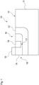
- Figure 1 shows an example of such a terminal structure.
- a transistor 10 comprising an epitaxial layer 11, also referred to as epi-layer 11 or drift layer in the following.
- the epi-layer 11 may be formed by n-type SiC.
- a well region 13 may be formed by doping the epi-layer 11 with a suitable dopant.
- a p-well may be formed by selectively doping the epi-layer 11 with an electron accepting element.
- a channel region of the transistor 10 is located within this well region 13.
- a terminal region 14, such as a source region, may be formed in part of the well region 13.
- the terminal region 14 typically has the same conductivity type as the epi-layer 11, but may have a higher doping concentration.
- an n++ source region may be formed by implanting dopants acting as electron donors.
- At least a part of the upper surface 12 of the terminal region 14 is in touch with a terminal electrode 15.
- a metallization layer may be used to connect an outside terminal to the terminal region 14.
- the terminal region 14 further comprises a resistive region 16.
- a resistive region has a resistivity that is considerably higher than the remaining parts of the terminal region 14. This is achieved, at least in part, by introduction of amphoteric impurities within the resistive region 16. Since amphoteric impurities can act both as donors and acceptors for charge carriers, it greatly reduces the conductivity of all kinds of doped semiconductor materials, including highly doped p++ or n++ regions of a SiC epi-layer.
- the resistive region 16 can take many different configurations. As shown in Figure 1 , it may extend from the upper surface 12 partly through the terminal region 14, thereby forming a relatively narrow connecting part 17 connecting a left and right sub-region 18 and 19 of the terminal region 14, respectively. Within the resistive region 16, the depletion of charge carriers by the amphoteric dopant reduces a current. Within the connecting part 17, due to its limited spatial extent, the overall current is also limited. Thus, a short-circuit current flowing through the epi-layer 11, the well region 13, the terminal region 14 and the terminal electrode 15 can be greatly reduced, with most of a corresponding voltage drop occurring within the terminal region 14.
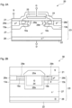
- Figure 2A and 2B show how such a terminal electrode can be used in a vertical power transistor.
- FIG. 2A shows a modified planar VDMOS 20.
- the VDMOS 20 comprises a source electrode 21 and a drain electrode 22 arranged on opposite surfaces of a semiconductor transistor structure 23. Between the source electrode 21 and the top surface of the semiconductor transistor structure 23, an insulated gate structure is formed, comprising a gate electrode 24 and surrounding insulation layers 25.
- the semiconductor transistor structure 23 comprises, from bottom to top, and a n + -type substrate layer 26 acting as drain region, an n - -type drift layer 27 corresponding to the epi-layer 11 of Fig.
- n+ buffer layer between the substrate layer 26 and the epi-layer 11, two p-type well regions 13a and 13b, two n + -type source regions 29a and 29b corresponding to the terminal region 14 of Figure 1 , and, in addition, two p + -type well contact regions 28a and 28b electrically connecting the source electrode 21 with the well regions 13a and 13b.
- each one of the source regions 29a and 29b comprises a resistive region 16a and 16b as explained above with regard to Figure 1 . That is to say, in the modified VDMOS 20 according to Figure 2 , the resistivity of both parts of the source regions 29a and 29b is increased and controlled as described above and below.
- Figure 2B shows a trench gate power transistor 30 comprising a gate electrode 24 in a trench arranged between two n + -type source regions 29a and 29b and p-type well regions 13a and 13b.
- the gate electrode is insulated by an upper insulation layer 25a from the source electrode 21 and by a lower insulation layer 25b from the semiconductor transistor structure 23.
- Most other components of the trench gate power transistor 30 correspond to the corresponding parts of the planar VDMOS 20 described above with respect to Figure 2A and are therefore not described here again.
- each one of the source regions 29a and 29b comprises a resistive region 16a and 16b, respectively, configured as a vertical sub-layer of the respective terminal regions 29a and 29b.
- resistive regions 16a and 16b shown in Figures 2A and 2B are presented as an example, and that other configurations, such as the configurations shown in Figures 14(a) to 15(g) may be used in each of the disclosed transistor devices.
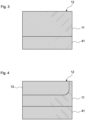
- a substrate 41 is provided.
- an n-type SiC substrate may be provided.
- the substrate 41 may correspond to a backside layer or drain region of the in the finished power transistor 40.
- Nitrogen (N) or Phosphorus (P) may be used as dopant for making n-type regions.
- a maximum doping concentrations of the drain region may lie in a range between 1 ⁇ 10 17 cm -3 and 5 ⁇ 10 20 cm -3 .
- an epi-layer 11 is grown on the substrate 41, as still shown in Figure 3 .
- an n-type SiC epi-layer may be grown on the substrate 41.
- the epi-layer 11 may correspond to a drift layer in the finished power transistor 40.
- a maximum doping concentration of the drift layer may be in a range between 1 ⁇ 10 14 cm -3 and 1 ⁇ 10 17 cm -3 .
- a photolithographic mask (not shown) may be formed on an upper surface 12 of the epi-layer 11 to selectively cover parts of the upper surface 12, before in a step S3 a remaining part of the surface 12 is doped using an appropriate dopant to form a well region 13.
- an appropriate dopant For example, Aluminum (Al), Boron (B) or Gallium (Ga) species, or any combination of the above, with or without n-type dopants, may be implanted to form a p-type well. That is to say, p-type regions may be formed by implantation of Al or B or Ga, but also by co-implanting Al/B, Al/Ga, B/Ga, or even by implanting Al/N, B/N etc.
- a maximum doping concentrations of the well region 13 may be 1 ⁇ 10 16 cm -3 or above.
- a modified or new mask may be used to form a well contact region 28.
- the well contact region 28 may be a p++-doped area.
- a maximum doping concentrations of the well contact region 28 may lie in a range between 1 ⁇ 10 17 cm -3 and 5 ⁇ 10 20 cm -3 .
- the well contact region 28 may prevent a floating of the electrical potential of the well region 13 during operation of the transistor device.
- a terminal region 14 may be formed using yet another photolithographic mask.
- a highly doped n++ region may be formed within the p-well region 13 to form a source region of the power transistor 40.
- a maximum doping concentrations of the source region may lie in a range between 1 ⁇ 10 17 cm -3 and 5 ⁇ 10 20 cm -3 .
- the terminal region 14 shown in Figure 6 may be formed by implantation of nitrogen (N) or phosphorus (P) into the SiC base material.
- the dopant species implanted in step S5 may be activated.
- the implanted dopants may be activated at a relatively high temperature, e.g. for 30 minutes at a temperature of 1600 °C.
- an amphoteric dopant is implanted in at least part of the terminal region 14 to form a resistive region 16. This may be achieved using another photolithographic mask (not shown).
- the SiC material of the epi-layer 11 is doped through one or more openings in the mask using an amphoteric dopant species.
- an amphoteric dopant species either Mn or V are used as dopants. However, in certain situations other amphoteric dopants may be used.
- Step S7 may be performed at room temperature with implantation energy chosen so that the depth d of the implanted amphoteric impurities matches the depths of the terminal region 14 as shown in Figure 7 .
- implantation energy chosen so that the depth d of the implanted amphoteric impurities matches the depths of the terminal region 14 as shown in Figure 7 .
- a lower implantation energy may be used to result in a shallower implantation of amphoteric impurities.
- an initial resistivity ⁇ of approximately 0.02 Qcm of an n++ source region may be increased by doping it with Mn or V to obtain an initial resistivity of about 20 kQcm.
- the presence of the deep Mn or V acceptor and donor levels in the respective upper and lower part of the SiC bandgap compensates the N donor or Al acceptor doping of the surrounding wide bandgap semiconductor material.
- the table below shows the location of the acceptor and donor levels of Mn and V with respect to the conduction band energy E C and the valence band energy E V .
- the use of amphoteric dopants allows the resistivity ⁇ of the resistive region 16 to be closely controlled in an optional annealing step S8. As shown in the logarithmic chart of Figure 10 , the resistivity ⁇ of the resistive region 16 can be controlled by selection of a corresponding annealing temperature T 1 .
- the resistivity ⁇ initially lies at about 20 kQcm. With increasing annealing temperature T 1 , applied for a given period of time, for example for 30 minutes, the resistivity ⁇ can be reduced to about 2 k ⁇ cm in the sample structure tested. Attention is drawn to the fact that the resistance of the terminal region 14 also depends on the implantation dose used during implantation of the amphoteric impurities. Thus, the resistance of the terminal region 14 may be controlled by at least two parameters during the manufacturing of the power transistor 40.
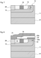
- one or more insulation layers and/or electrodes may be formed on the upper surface 12 of the epi-layer 11.
- an insulation layer 25a was formed over parts of the terminal region 14, the part of the well region 13 near the upper surface 12 later forming a channel region 42 of the transistor structure (dashed in Figure 8 ), as well as a neighbouring area of the epi-layer 11.
- a gate electrode 24 is formed on top of the first insulation layer 25a.
- the gate electrode 24 is then covered by a second insulation layer 25b, which insulates a top surface of the gate electrode 24.
- a source electrode 21 is formed on the remaining part of the upper surface 12 of the epi-layer 11 in the area of the well contact region 28 and parts of the terminal region 14. As shown in Figure 8 , the source electrode 21 also covers an upper surface of the second insulation layer 25b, as is commonly the case in vertical power transistors 40.
- Figure 9 shows a cross-section through part of the finished vertical power transistor 40 after formation of a drain electrode 22 on an opposite back side 43 of the substrate 41.
- Figure 9 also shows a current path 44 from the drain electrode 22, through the substrate 41, a drift layer formed by the epi-layer 11, the p-well region 13, including the channel region 42 (dashed), the terminal region 14, comprising two different n++ sub-regions 18, 19 without amphoteric dopants and another sub-region in the form of the resistive region 16, to the source electrode 21.
- a short circuit current can be controlled without overly increasing the total source-to-drain resistance RDSon during normal operation.
- TCAD Technology computer-aided design
- Figure 11 shows, in a linear chart, the J D /V DS characteristics of the power transistor 40
- Figure 12 shows, in a linear chart, the simulated electro-thermal short-circuit current density waveform J D over time t.
- a semiconductor device experiences an energy which is directly related to the maximum value of the current I MAX .
- the disclosed design improves the SCWT with a minimal impact of the source-to-drain resistivity RDSon.
- the reduction of maximum or peak current I MAX is due to the presence of the implanted amphoteric impurities in the resistive region 16. Since the implantation is performed in the source region, it does not affect the channel region 42.
- Figure 13 shows, in a linear chart, the transfer characteristics of the power transistor 40. Attention is drawn to the fact that characteristics of the power transistor 40 with different depths d of a resistive region coincide for the characteristic J D /V GS curve of the reference design without amphoteric dopants, confirming that the threshold voltage value is not affected.
- Figures 14 and 15 show various configurations of a terminal region 14 with one or more resistive regions 16 formed therein. Attention is drawn to the fact that amphoteric impurities do not diffuse in the used wide bandgap semiconductor material and thereby stay localized in the resistive regions 16 after doping. Thus, by using conventional doping techniques, different patterns can be achieved as shown.
- a horizontal segmentation shown in Figure 14 (a) may be used.
- a single resistive region 16 may be formed as shown in Figure 14 (a) , or multiple resistive regions 16 separated by intermediate parts of the terminal region 14 not implanted with amphoteric impurities as shown in Figure 14 (b) may be used.
- individual parts of the resistive region 16 can be located at an upper surface 12 or embedded deeper in the terminal region as shown, for example, to generate a chessboard pattern as shown in Figure 14 (c) or separated islands of amphoteric dopants as shown in Figure 14 (d) .
- a horizontal separation as already explained above with regard to Figure 7 can also comprise multiple resistive regions 16 as shown in Figure 14 (e) .
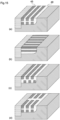
- Figures 15 (a) to 15 (g) show the formation of various first (darker) sub-regions 45 of the terminal region 14 doped with amphoteric impurities and second (lighter) sub-regions 46 of the terminal region 14 essentially free of amphoteric impurities.
- Such designs may be obtained, for example, by suitable masks or interference patterns used during implantation of the amphoteric species or a combination thereof.
- the dimensions and implementation depths d and resistivity of the resistive regions 16 can be adjusted to extend along the entire depths of the terminal region 14 by varying the implantation energy within the range of, for example, 50 to 500 keV and/or by adjusting the doses, for example in the range of 10 11 to 10 14 cm -2 .
- the disclosed transistor structures and manufacturing techniques result in a number of benefits.
- amphoteric impurities can be implanted irrespective of used base material, such as those used for forming and doping an n++ or p++ source or drain region. This enables, among others, that the implantation energy of the chosen amphoteric species can remain the same, irrespective of the dopant used for doping a corresponding terminal region, such as N, P, Al or B.
- FIG. 1 to 16 represent exemplary embodiments of an improved transistor structure and method for its manufacturing. Therefore, they do not constitute a complete list of all embodiments according to the improved devices and/or methods. Actual devices, systems and methods may vary from the embodiments shown in terms of the semiconductor base materials, dopants, and processing parameters, for example.
Landscapes
- Metal-Oxide And Bipolar Metal-Oxide Semiconductor Integrated Circuits (AREA)
- Junction Field-Effect Transistors (AREA)
- Semiconductor Integrated Circuits (AREA)
- Thyristors (AREA)
- Electrodes Of Semiconductors (AREA)
Abstract
Description
- The present disclosure relates to a transistor, in particular a wide bandgap power transistor, comprising an epitaxial layer, at least one well region and at least one terminal region, in particular a source region. The present disclosure further relates to a power electronic switching device comprising a plurality of switching cells and a method for manufacturing a transistor, in particular a SiC power transistor.
- Transistors are used in many applications, including power electronics. It is generally desirable for transistors, such as Metal-Oxide-Semiconductor Field Effect Transistor (MOSFETs), to be able to withstand so-called short-circuit conditions for a specified time. For example, it may be desirable to provide power transistors with a short-circuit withstand time (SCWT) of at least 10 µs. The SCWT may be used by a control circuit to identify a fault in a corresponding power circuit and to de-energize it.
- At the same time, it is desirable to minimize conduction losses of transistors, and in particular of power transistors. Low conduction losses generally lead to higher saturation current densities in the semiconductor material, which in turn shortens their SCWT.
- Accordingly, it is a challenge to describe improved devices and methods for their manufacturing which allow to balance the aim of low conduction losses with the aim of a predetermined SCWT.
- Embodiments of the disclosure relate to a transistor, a power electronic switching device and a method for manufacturing a transistor that allow to selectively increase the resistivity inside one of the terminal regions to control a voltage drop within the transistor structure and thus control a corresponding SCWT of the transistor. This is achieved, at least in part, by introduction of at least one resistive region comprising amphoteric impurities.
- According to a first aspect, a transistor, in particular a wide bandgap semiconductor power transistor, is disclosed. The transistor comprises an epitaxial layer of a first conductivity type, at least one well region of a second conductivity type formed in a selected area of the epitaxial layer, at least one terminal region, in particular a source region, of the first conductivity type formed in or adjacent to the at least one well region, at least one terminal electrode, in particular a source electrode, formed at least partly on a surface of a first part of the at least one terminal region, and at least one resistive region formed within the at least one terminal region, the at least one resistive region comprising amphoteric impurities.
- By introducing at least one resistive region formed within at least one terminal region, a resistance of the terminal region can be increased and other parts of the transistor structure can be protected by reducing a voltage drop therein. The use of amphoteric impurities allows to closely control the resistivity of the resistive region and, therefore, the overall resistance of the terminal region.
- Among others, the inventors have found that the resistivity of a terminal region implanted with amphoteric species can be controlled, for example, based on the implantation dose or an activation temperature of the resistive region.
- The at least one resistive region may comprise at least one of manganese (Mn), and vanadium (V) as amphoteric dopants. These dopants may operate, selectively, as charge acceptors or donors in common wide bandgap semiconductor materials useful for power electronics, in particular in silicon carbide (SiC), such as 4H-SiC or 6H-SiC.
- Using common semiconductor processing steps and parameters, the resistivity of the terminal region can be modulated to lie in excess of 10 Qcm, for example somewhere in the range between 20 Qcm and 20 kQcm, which is a useful range for controlling the SCWT of a power transistor.
- Different structures within the terminal region may be obtained by using various implantation techniques. For example, it is possible to fully separate second sub-regions of the terminal region comprising essentially no amphoteric impurities by one or more first sub-region in which an amphoteric impurity is present. By patterning the at least one terminal region, the current density in different parts of the terminal region can be closely controlled.
- The described terminal structure is applicable to many different transistor types, including metal-oxide-semiconductor field-effect transistors (MOSFETs), metal-insulator-semiconductor field-effect transistors (MISFETs), junction field-effect transistors (JFETs) and insulated gate bipolar transistors (IGBTs). Moreover, the described terminal structure can be used in different configurations, including planar and trench configurations.
- According to a second aspect, a power electronic switching device is disclosed. The device comprises a plurality of switching cells electrically connected in parallel, wherein each switching cell of the plurality of switching cells comprises a transistor according to the first aspect. By using several of the above transistors in parallel, a relatively high current rating can be obtained, as often required in power electronics.
- Features and advantages described in connection with an individual transistor may also be used in more complex devices, such as power electronic switching devices comprising a plurality of transistor cells arranged on a common substrate and/or electrically connected in parallel.
- The transistor or power electronic switching devices according to the above aspects may have a voltage rating of 600 Volts or above.
- According to a third aspect, a method for manufacturing a transistor, in particular a wide bandgap semiconductor power transistor, is provided. The method comprises the steps of:
- epitaxially growing a semiconductor layer of a first conductivity type;
- forming at least one well region of a second conductivity type formed in a selected area of the epitaxial layer;
- forming at least one terminal region, in particular a source region, of the first conductivity type in or adjacent to the at least one well region; and
- implanting an amphoteric dopant in at least a part of the at least one terminal region.
- The above steps allow to manufacture a transistor according to the first aspect using well-established processing steps used in the manufacturing of power electrical devices.
- For example, an implantation depth of the amphoteric dopant and thus the shape of the resistive region may be controlled using appropriate implantation energies in the range of 50 to 1000 keV.
- Moreover, the overall resistivity of the resistive region can be controlled by implanting the amphoteric dopant using an implantation dose in the range of 1010 cm-2 to 1014 cm-2.
- In at least one embodiment, the method further comprises annealing at least one resistive region comprising the implanted amphoteric dopants at a first temperature T1, wherein the first temperature T1 is selected based on a target resistivity ρ of the terminal region. According to experiments by the inventors, there is a relationship between an activation temperature and the resistivity of the doped and activated resistive regions, which can be exploited to limit a peak current through the transistor during short-circuit conditions. In particular, if a source region is doped with the amphoteric dopant, a current density in a neighbouring channel region can be reduced, which is defined by the gate-to-source potential (VGS) in power transistors.
- The present disclosure comprises several aspects of a semiconductor device, in particular a terminal structure of a transistor, and a method for manufacturing such a transistor and terminal. Every feature described with respect to one of the aspects is also disclosed herein with respect to the other aspects, even if the respective feature is not explicitly mentioned in the context of the specific aspect.
- The accompanying figures are included to provide a further understanding. In the figures, elements of the same structure and/or functionality may be referenced by the same reference signs. It is to be understood that the embodiments shown in the figures are illustrative representations and are not necessarily drawn to scale.
-
Figure 1 shows a schematic cross-section through a terminal region of a transistor. -
Figures 2a and 2B shows schematic cross-sections through vertical power transistors in a planar and trench configuration, respectively. -
Figures 3 to 9 show various steps of a process for manufacturing a vertical power MOSFET. -
Figure 10 shows a relationship between the resistivity of a semiconductor region with amphoteric impurities in dependence on an annealing temperature. -
Figures 11 to 13 show different characteristics of a transistor device comprising a resistive region with amphoteric impurities. -
Figure 14 shows cross-sections through five potential configurations of a terminal region. -
Figure 15 shows perspective views of seven further potential configurations of a terminal region. -
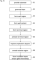
Figure 16 shows steps of a method for manufacturing a transistor. - While the disclosed invention is applicable to many different types of semiconductor transistors, a particular focus is placed on power MISFETs, in particular power MISFETs implemented using wide bandgap semiconductor materials, such as SiC. An important feature of a MISFET is the ability to withstand short circuit conditions for a given time, e.g. more than 10 µs. During this time, the so-called short-circuit withstand time (SCWT), associated control circuit can identify and de-energize the fault. In power electronics, SiC MISFETs are typically designed with relatively short channel length and small pitches between neighboring switching cells. Such a compact design is beneficial to minimize conduction losses of individual transistors as well as complex power electronic switching devices. On the other hand, this leads to relatively high saturation current densities which, in turn, shorten the SCWT.
- To achieve a desired design trade-off between low conduction losses and a desired SCWT, according to at least one implementation example, a terminal region of a SiC MISFET, for example an n++ source region, is implanted with a high resistive region, in order to obtain a trade-off between conduction losses and SCWT. The resistivity ρ of the high resistive region can be modulated by various processing parameters as described below.
-
Figure 1 shows an example of such a terminal structure. In particular, it shows a cross-section through part of atransistor 10 comprising anepitaxial layer 11, also referred to as epi-layer 11 or drift layer in the following. The epi-layer 11 may be formed by n-type SiC. In a part of the epi-layer 11 close to its front side orupper surface 12, awell region 13 may be formed by doping the epi-layer 11 with a suitable dopant. For example, a p-well may be formed by selectively doping the epi-layer 11 with an electron accepting element. In the example presented inFigure 1 , a channel region of thetransistor 10 is located within thiswell region 13. In a following processing step, aterminal region 14, such as a source region, may be formed in part of thewell region 13. Theterminal region 14 typically has the same conductivity type as the epi-layer 11, but may have a higher doping concentration. For example, an n++ source region may be formed by implanting dopants acting as electron donors. At least a part of theupper surface 12 of theterminal region 14 is in touch with aterminal electrode 15. For example, a metallization layer may be used to connect an outside terminal to theterminal region 14. - In the described example, the
terminal region 14 further comprises aresistive region 16. In the sense of this disclosure, a resistive region has a resistivity that is considerably higher than the remaining parts of theterminal region 14. This is achieved, at least in part, by introduction of amphoteric impurities within theresistive region 16. Since amphoteric impurities can act both as donors and acceptors for charge carriers, it greatly reduces the conductivity of all kinds of doped semiconductor materials, including highly doped p++ or n++ regions of a SiC epi-layer. - The
resistive region 16 can take many different configurations. As shown inFigure 1 , it may extend from theupper surface 12 partly through theterminal region 14, thereby forming a relatively narrow connectingpart 17 connecting a left andright sub-region terminal region 14, respectively. Within theresistive region 16, the depletion of charge carriers by the amphoteric dopant reduces a current. Within the connectingpart 17, due to its limited spatial extent, the overall current is also limited. Thus, a short-circuit current flowing through the epi-layer 11, thewell region 13, theterminal region 14 and theterminal electrode 15 can be greatly reduced, with most of a corresponding voltage drop occurring within theterminal region 14. -
Figure 2A and 2B show how such a terminal electrode can be used in a vertical power transistor. - In particular,
Figure 2A shows a modifiedplanar VDMOS 20. TheVDMOS 20 comprises asource electrode 21 and adrain electrode 22 arranged on opposite surfaces of asemiconductor transistor structure 23. Between thesource electrode 21 and the top surface of thesemiconductor transistor structure 23, an insulated gate structure is formed, comprising agate electrode 24 and surrounding insulation layers 25. Thesemiconductor transistor structure 23 comprises, from bottom to top, and a n+-type substrate layer 26 acting as drain region, an n--type drift layer 27 corresponding to the epi-layer 11 ofFig. 1 , an optional n+ buffer layer (not shown) between thesubstrate layer 26 and the epi-layer 11, two p-type well regions type source regions terminal region 14 ofFigure 1 , and, in addition, two p+-typewell contact regions source electrode 21 with thewell regions - In the example presented in
Figure 2A , each one of thesource regions resistive region Figure 1 . That is to say, in the modifiedVDMOS 20 according toFigure 2 , the resistivity of both parts of thesource regions -
Figure 2B shows a trenchgate power transistor 30 comprising agate electrode 24 in a trench arranged between two n+-type source regions type well regions upper insulation layer 25a from thesource electrode 21 and by alower insulation layer 25b from thesemiconductor transistor structure 23. Most other components of the trenchgate power transistor 30 correspond to the corresponding parts of theplanar VDMOS 20 described above with respect toFigure 2A and are therefore not described here again. - In the example presented in
Figure 2B , each one of thesource regions resistive region respective terminal regions - It is noted that the specific configurations of the
resistive regions Figures 2A and 2B are presented as an example, and that other configurations, such as the configurations shown inFigures 14(a) to 15(g) may be used in each of the disclosed transistor devices. - Next, with reference to
Figures 3 to 9 as well as the flowchart according toFigure 16 , various stages in the manufacturing of apower transistor 40, such as a vertical power MOSFET, will be explained. - Referring first to
Figure 3 , in a first step S1, asubstrate 41 is provided. For example, an n-type SiC substrate may be provided. Thesubstrate 41 may correspond to a backside layer or drain region of the in thefinished power transistor 40. For example, Nitrogen (N) or Phosphorus (P) may be used as dopant for making n-type regions. A maximum doping concentrations of the drain region may lie in a range between 1·1017 cm-3 and 5·1020 cm-3. - In a subsequent step S2, an epi-
layer 11 is grown on thesubstrate 41, as still shown inFigure 3 . In the described example, an n-type SiC epi-layer may be grown on thesubstrate 41. The epi-layer 11 may correspond to a drift layer in thefinished power transistor 40. Depending on the voltage class of thepower transistor 40, a maximum doping concentration of the drift layer may be in a range between 1·1014 cm-3 and 1·1017 cm-3. - Referring next to
Figure 4 , a photolithographic mask (not shown) may be formed on anupper surface 12 of the epi-layer 11 to selectively cover parts of theupper surface 12, before in a step S3 a remaining part of thesurface 12 is doped using an appropriate dopant to form awell region 13. For example, Aluminum (Al), Boron (B) or Gallium (Ga) species, or any combination of the above, with or without n-type dopants, may be implanted to form a p-type well. That is to say, p-type regions may be formed by implantation of Al or B or Ga, but also by co-implanting Al/B, Al/Ga, B/Ga, or even by implanting Al/N, B/N etc. A maximum doping concentrations of thewell region 13 may be 1·1016 cm-3 or above. - Referring next to
Figure 5 , in an optional step S4, a modified or new mask may be used to form awell contact region 28. Thewell contact region 28 may be a p++-doped area. A maximum doping concentrations of thewell contact region 28 may lie in a range between 1·1017 cm-3 and 5·1020 cm-3. In thefinished power transistor 40, thewell contact region 28 may prevent a floating of the electrical potential of thewell region 13 during operation of the transistor device. - Referring next to
Figure 6 , in a step S5, aterminal region 14 may be formed using yet another photolithographic mask. For example, a highly doped n++ region may be formed within the p-well region 13 to form a source region of thepower transistor 40. A maximum doping concentrations of the source region may lie in a range between 1·1017 cm-3 and 5·1020 cm-3. Theterminal region 14 shown inFigure 6 may be formed by implantation of nitrogen (N) or phosphorus (P) into the SiC base material. - Then, in a further step S6, the dopant species implanted in step S5 may be activated. For example, the implanted dopants may be activated at a relatively high temperature, e.g. for 30 minutes at a temperature of 1600 °C.
- Referring next to
Figure 7 , in a further step S7 an amphoteric dopant is implanted in at least part of theterminal region 14 to form aresistive region 16. This may be achieved using another photolithographic mask (not shown). The SiC material of the epi-layer 11 is doped through one or more openings in the mask using an amphoteric dopant species. In the described process, either Mn or V are used as dopants. However, in certain situations other amphoteric dopants may be used. - For example, ion implantation and/or plasma ion implantation may be used. Step S7 may be performed at room temperature with implantation energy chosen so that the depth d of the implanted amphoteric impurities matches the depths of the
terminal region 14 as shown inFigure 7 . Alternatively, a lower implantation energy may be used to result in a shallower implantation of amphoteric impurities. - The introduction of amphoteric impurities greatly increases the resistivity of the
terminal region 14 within theresistive region 16. For example, an initial resistivity ρ of approximately 0.02 Qcm of an n++ source region may be increased by doping it with Mn or V to obtain an initial resistivity of about 20 kQcm. The presence of the deep Mn or V acceptor and donor levels in the respective upper and lower part of the SiC bandgap compensates the N donor or Al acceptor doping of the surrounding wide bandgap semiconductor material. The table below shows the location of the acceptor and donor levels of Mn and V with respect to the conduction band energy EC and the valence band energy EV.Dopant species Donor level Acceptor level Mn EC - 1.38 eV EC - 0.68 eV V EC - 1.47 eV EC - 0.70 eV - Among others, the use of amphoteric dopants allows the resistivity ρ of the
resistive region 16 to be closely controlled in an optional annealing step S8. As shown in the logarithmic chart ofFigure 10 , the resistivity ρ of theresistive region 16 can be controlled by selection of a corresponding annealing temperature T1. - Without annealing, the resistivity ρ initially lies at about 20 kQcm. With increasing annealing temperature T1, applied for a given period of time, for example for 30 minutes, the resistivity ρ can be reduced to about 2 kΩcm in the sample structure tested. Attention is drawn to the fact that the resistance of the
terminal region 14 also depends on the implantation dose used during implantation of the amphoteric impurities. Thus, the resistance of theterminal region 14 may be controlled by at least two parameters during the manufacturing of thepower transistor 40. - Referring next to
Figure 8 , in a further step S9, one or more insulation layers and/or electrodes may be formed on theupper surface 12 of the epi-layer 11. - In the configuration shown in
Figure 8 , at first aninsulation layer 25a was formed over parts of theterminal region 14, the part of thewell region 13 near theupper surface 12 later forming achannel region 42 of the transistor structure (dashed inFigure 8 ), as well as a neighbouring area of the epi-layer 11. On top of thefirst insulation layer 25a, agate electrode 24 is formed. Thegate electrode 24 is then covered by asecond insulation layer 25b, which insulates a top surface of thegate electrode 24. - Thereafter, a
source electrode 21 is formed on the remaining part of theupper surface 12 of the epi-layer 11 in the area of thewell contact region 28 and parts of theterminal region 14. As shown inFigure 8 , thesource electrode 21 also covers an upper surface of thesecond insulation layer 25b, as is commonly the case invertical power transistors 40. -
Figure 9 shows a cross-section through part of the finishedvertical power transistor 40 after formation of adrain electrode 22 on an opposite backside 43 of thesubstrate 41. -
Figure 9 also shows a current path 44 from thedrain electrode 22, through thesubstrate 41, a drift layer formed by the epi-layer 11, the p-well region 13, including the channel region 42 (dashed), theterminal region 14, comprising twodifferent n++ sub-regions resistive region 16, to thesource electrode 21. By modulating the resistivity ρ of theresistive region 16 and hence of theterminal region 14, a short circuit current can be controlled without overly increasing the total source-to-drain resistance RDSon during normal operation. - Technology computer-aided design (TCAD) simulations have been used to prove the proposed solution; the results are shown in
Figures 11 to 13 . - In particular,
Figure 11 shows, in a linear chart, the JD/VDS characteristics of thepower transistor 40, andFigure 12 shows, in a linear chart, the simulated electro-thermal short-circuit current density waveform JD over time t. It can be seen that, compared to a reference design without the additional amphoteric implantation, the RDSon increases by about 9% (Figure 11 ), while the peak of the SC current is reduced by approximately 18% (Figure 12 ). Therefore the trade-off between conduction losses and SCWT is improved. - In general, during a short-circuit condition, a semiconductor device experiences an energy which is directly related to the maximum value of the current IMAX. As shown in
Figures 11 and12 , the disclosed design improves the SCWT with a minimal impact of the source-to-drain resistivity RDSon. The reduction of maximum or peak current IMAX is due to the presence of the implanted amphoteric impurities in theresistive region 16. Since the implantation is performed in the source region, it does not affect thechannel region 42. -
Figure 13 shows, in a linear chart, the transfer characteristics of thepower transistor 40. Attention is drawn to the fact that characteristics of thepower transistor 40 with different depths d of a resistive region coincide for the characteristic JD/VGS curve of the reference design without amphoteric dopants, confirming that the threshold voltage value is not affected. -
Figures 14 and15 show various configurations of aterminal region 14 with one or moreresistive regions 16 formed therein. Attention is drawn to the fact that amphoteric impurities do not diffuse in the used wide bandgap semiconductor material and thereby stay localized in theresistive regions 16 after doping. Thus, by using conventional doping techniques, different patterns can be achieved as shown. - For example, as an alternative to the vertical segmentation shown in
Figure 7 , a horizontal segmentation shown inFigure 14 (a) may be used. For example, a singleresistive region 16 may be formed as shown inFigure 14 (a) , or multipleresistive regions 16 separated by intermediate parts of theterminal region 14 not implanted with amphoteric impurities as shown inFigure 14 (b) may be used. Moreover, due to the selection of implantation energies, individual parts of theresistive region 16 can be located at anupper surface 12 or embedded deeper in the terminal region as shown, for example, to generate a chessboard pattern as shown inFigure 14 (c) or separated islands of amphoteric dopants as shown inFigure 14 (d) . Of course, a horizontal separation as already explained above with regard toFigure 7 can also comprise multipleresistive regions 16 as shown inFigure 14 (e) . -
Figures 15 (a) to 15 (g) show the formation of various first (darker)sub-regions 45 of theterminal region 14 doped with amphoteric impurities and second (lighter)sub-regions 46 of theterminal region 14 essentially free of amphoteric impurities. Such designs may be obtained, for example, by suitable masks or interference patterns used during implantation of the amphoteric species or a combination thereof. - The dimensions and implementation depths d and resistivity of the
resistive regions 16 can be adjusted to extend along the entire depths of theterminal region 14 by varying the implantation energy within the range of, for example, 50 to 500 keV and/or by adjusting the doses, for example in the range of 1011 to 1014 cm-2. - The disclosed transistor structures and manufacturing techniques result in a number of benefits. This includes the modulation of the resistivity ρ of a
terminal region 14, such as a source region, in order to adjust and control the trade-off between conduction losses and SCWT. Moreover, amphoteric impurities can be implanted irrespective of used base material, such as those used for forming and doping an n++ or p++ source or drain region. This enables, among others, that the implantation energy of the chosen amphoteric species can remain the same, irrespective of the dopant used for doping a corresponding terminal region, such as N, P, Al or B. - The embodiments shown in
Figures 1 to 16 as stated represent exemplary embodiments of an improved transistor structure and method for its manufacturing. Therefore, they do not constitute a complete list of all embodiments according to the improved devices and/or methods. Actual devices, systems and methods may vary from the embodiments shown in terms of the semiconductor base materials, dopants, and processing parameters, for example. -
- 10
- transistor
- 11
- epitaxial layer
- 12
- upper surface
- 13
- well region
- 14
- terminal region
- 15
- terminal electrode
- 16
- resistive region
- 17
- connecting part
- 18
- left sub-region
- 19
- right sub-region
- 20
- VDMOS
- 21
- source electrode
- 22
- drain electrode
- 23
- semiconductor transistor structure
- 24
- gate electrode
- 25
- insulation layer
- 26
- substrate layer
- 27
- drift layer
- 28
- well contact region
- 29
- source region
- 30
- trench gate power transistor
- 40
- power transistor
- 41
- substrate
- 42
- channel area
- 43
- back side
- 44
- current path
- 45
- first sub-region (amphoteric)
- 46
- second sub-region (non-amphoteric)
Claims (15)
- A transistor (10), in particular a wide bandgap semiconductor power transistor (40), comprising:- an epitaxial layer (11) of a first conductivity type;- at least one well region (13) of a second conductivity type formed in a selected area of the epitaxial layer (11) ;- at least one terminal region (14), in particular a source region (29), of the first conductivity type formed in or adjacent to the at least one well region (13) ;- at least one terminal electrode (15), in particular a source electrode (21), formed at least partly on a surface (12) of a first part of the at least one terminal region (14); and- at least one resistive region (16) formed within the at least one terminal region (14), the at least one resistive region (16) comprising amphoteric impurities.
- The transistor (10) of claim 1, wherein the at least one resistive region (16) comprises at least one of Manganese, Mn, and Vanadium, V, as amphoteric dopants.
- The transistor (10) of claim 1 or 2, wherein a concentration of amphoteric dopants in the at least one resistive region (16) lies in the range of 1014 to 1018 cm-3.
- The transistor (10) of any one of claims 1 to 3, wherein- a resistivity ρ of the terminal region (14) exceeds 10 Qcm, and preferably lies in the range of 20Ωcm to 20 kQcm.
- The transistor (10) of any one of claims 1 to 4, wherein a short-circuit withstand time, SCWT, of the transistor exceeds 3 µs, and preferably is or exceeds 10 µs.
- The transistor (10) of any one of claims 1 to 5, wherein- an implantation depth d of the at least one resistive region (16) lies in the range of 0 to 100%, preferably in the range of 10% to 100%, of the maximal thickness of the at least one terminal region (14).
- The transistor (10) of any one of claims 1 to 6, wherein the at least one terminal region (14) comprises at least three sub-regions, comprising at least one first sub-region (45) comprising amphoteric impurities and at least one second sub-region (18, 19, 46) essentially free of amphoteric impurities, in particular one of:- one first sub-region (45) arranged horizontally between and/or separating two adjacent second sub-regions (18, 19, 46) ;- one first sub-region (45) arranged vertically between and/or separating two adjacent second sub-regions (46);- a plurality of first sub-regions (45) partially or completely embedded as resistive islands in a common second sub-region (46); and- a first plurality of first sub-regions (45) and a second plurality of second sub-regions (46) forming at least one of a horizontal grid, a vertical grid, a comb structure, and a chess-board pattern.
- The transistor (10) of any one of claims 1 to 7, wherein the transistor (10) is one of a metal-oxide-semiconductor field-effect transistor, MOSFET, a metal-insulator-semiconductor field-effect transistor, MISFET, a junction field-effect transistor, JFET, and an insulated-gate bipolar transistor, IGBT, in one of a planar or a trench configuration.
- The transistor (10) of any one of claims 1 to 8, further comprising at least one of the following:- a substrate (41) of the first conductivity region carrying the epitaxial layer (11);- at least one highly doped well contact region (28) of the second conductivity type, electrically connecting the at least one well region (13) with the at least one terminal electrode (15);- a second terminal region and a second electrode formed at least partly on a surface of the second terminal region;- at least one channel region (42) formed within the at least one well region (13) in proximity to a gate structure (23); and- a first insulation layer (25a) formed on a surface (12) of the epitaxial layer (11) and a gate electrode (24) formed on a surface of the first insulation layer (25a).
- A power electronic switching device, comprising a plurality of transistor cells arranged on a common substrate and/or electrically connected in parallel, each transistor cell comprising a transistor (10) according to one of claims 1 to 9.
- A method for manufacturing a transistor (10), in particular a wide bandgap semiconductor power transistor (40), comprising:- epitaxially growing (S2) a semiconductor layer of a first conductivity type;- forming (S3) at least one well region (13) of a second conductivity type formed in a selected area of the epitaxial layer (11);- forming (S5) at least one terminal region (14), in particular a source region (29), of the first conductivity type in or adjacent to the at least one well region (13); and- implanting (S7) an amphoteric dopant in at least a part of the at least one terminal region (14).
- The method of claim 11, wherein the amphoteric dopant is implanted using an implantation energy in the range of 50 to 1000 keV.
- The method of claim 11 or 12, wherein the amphoteric dopant is implanted using an implantation dose in the range of 1010 cm-2 to 1014 cm-2.
- The method of any one of claims 11 to 13, further comprising:- annealing (S8) at least one resistive region (16) comprising the implanted amphoteric dopants at a first temperature T1, wherein the first temperature T1 is selected based on a target resistivity ρ of the terminal region (14) .
- The method of claim 14, further comprising:- prior to annealing (S8) the at least one resistive region (16), activating (S6) the at least one terminal region (14) at a second temperature T2 exceeding the first temperature T1; and/or- after implanting (S7) the amphoteric dopant, forming (S9) at least one terminal electrode (15), in particular a source electrode (21), at least partly on a surface (12) of at least part of the at least one terminal region 16).
Priority Applications (5)
| Application Number | Priority Date | Filing Date | Title |
|---|---|---|---|
| EP22157298.5A EP4231358B1 (en) | 2022-02-17 | 2022-02-17 | Transistor, power electronic switching device and method for manufacturing a transistor |
| US18/836,320 US20250151341A1 (en) | 2022-02-17 | 2023-01-25 | Transistor, power electronic switching device and method for manufacturing a transistor |
| PCT/EP2023/051782 WO2023156158A1 (en) | 2022-02-17 | 2023-01-25 | Transistor, power electronic switching device and method for manufacturing a transistor |
| JP2024548624A JP7796241B2 (en) | 2022-02-17 | 2023-01-25 | Transistor, power electronic switch device, and method for manufacturing transistor |
| CN202380022138.9A CN118715598A (en) | 2022-02-17 | 2023-01-25 | Transistor, power electronic switching device and method for manufacturing transistor |
Applications Claiming Priority (1)
| Application Number | Priority Date | Filing Date | Title |
|---|---|---|---|
| EP22157298.5A EP4231358B1 (en) | 2022-02-17 | 2022-02-17 | Transistor, power electronic switching device and method for manufacturing a transistor |
Publications (2)
| Publication Number | Publication Date |
|---|---|
| EP4231358A1 true EP4231358A1 (en) | 2023-08-23 |
| EP4231358B1 EP4231358B1 (en) | 2024-05-22 |
Family
ID=80683033
Family Applications (1)
| Application Number | Title | Priority Date | Filing Date |
|---|---|---|---|
| EP22157298.5A Active EP4231358B1 (en) | 2022-02-17 | 2022-02-17 | Transistor, power electronic switching device and method for manufacturing a transistor |
Country Status (5)
| Country | Link |
|---|---|
| US (1) | US20250151341A1 (en) |
| EP (1) | EP4231358B1 (en) |
| JP (1) | JP7796241B2 (en) |
| CN (1) | CN118715598A (en) |
| WO (1) | WO2023156158A1 (en) |
Citations (3)
| Publication number | Priority date | Publication date | Assignee | Title |
|---|---|---|---|---|
| JP3848700B2 (en) * | 1996-05-10 | 2006-11-22 | 株式会社イオン工学研究所 | Silicon carbide semiconductor device |
| US20110012133A1 (en) * | 2008-03-07 | 2011-01-20 | Mitsubishi Electric Corporation | Silicon carbide semiconductor device and method for manufacturing the same |
| US20200286991A1 (en) * | 2019-03-07 | 2020-09-10 | Infineon Technologies Ag | Semiconductor Device Including Trench Structure and Manufacturing Method |
Family Cites Families (9)
| Publication number | Priority date | Publication date | Assignee | Title |
|---|---|---|---|---|
| EP1050908B1 (en) * | 1998-01-22 | 2016-01-20 | Mitsubishi Denki Kabushiki Kaisha | Insulating gate type bipolar semiconductor device |
| JP5417790B2 (en) * | 2007-12-04 | 2014-02-19 | 日産自動車株式会社 | Semiconductor device |
| JP5577607B2 (en) * | 2009-03-05 | 2014-08-27 | 日産自動車株式会社 | Semiconductor device and manufacturing method of semiconductor device |
| JP6132478B2 (en) * | 2012-05-09 | 2017-05-24 | 三菱電機株式会社 | Semiconductor device |
| WO2016063644A1 (en) * | 2014-10-20 | 2016-04-28 | 三菱電機株式会社 | Semiconductor device |
| JP6584881B2 (en) * | 2015-09-11 | 2019-10-02 | 株式会社東芝 | Semiconductor device |
| JP6336165B2 (en) * | 2017-03-14 | 2018-06-06 | 三菱電機株式会社 | Semiconductor device |
| JP6933339B2 (en) * | 2017-10-18 | 2021-09-08 | 矢崎総業株式会社 | Semiconductor devices and semiconductor wafers |
| WO2023119485A1 (en) * | 2021-12-22 | 2023-06-29 | 三菱電機株式会社 | Silicon carbide semiconductor device and method for producing silicon carbide semiconductor device |
-
2022
- 2022-02-17 EP EP22157298.5A patent/EP4231358B1/en active Active
-
2023
- 2023-01-25 JP JP2024548624A patent/JP7796241B2/en active Active
- 2023-01-25 US US18/836,320 patent/US20250151341A1/en active Pending
- 2023-01-25 WO PCT/EP2023/051782 patent/WO2023156158A1/en not_active Ceased
- 2023-01-25 CN CN202380022138.9A patent/CN118715598A/en active Pending
Patent Citations (3)
| Publication number | Priority date | Publication date | Assignee | Title |
|---|---|---|---|---|
| JP3848700B2 (en) * | 1996-05-10 | 2006-11-22 | 株式会社イオン工学研究所 | Silicon carbide semiconductor device |
| US20110012133A1 (en) * | 2008-03-07 | 2011-01-20 | Mitsubishi Electric Corporation | Silicon carbide semiconductor device and method for manufacturing the same |
| US20200286991A1 (en) * | 2019-03-07 | 2020-09-10 | Infineon Technologies Ag | Semiconductor Device Including Trench Structure and Manufacturing Method |
Also Published As
| Publication number | Publication date |
|---|---|
| EP4231358B1 (en) | 2024-05-22 |
| US20250151341A1 (en) | 2025-05-08 |
| JP7796241B2 (en) | 2026-01-08 |
| JP2025506062A (en) | 2025-03-05 |
| WO2023156158A1 (en) | 2023-08-24 |
| CN118715598A (en) | 2024-09-27 |
Similar Documents
| Publication | Publication Date | Title |
|---|---|---|
| US11837629B2 (en) | Power semiconductor devices having gate trenches and buried edge terminations and related methods | |
| JP7674407B2 (en) | Power silicon carbide MOSFET devices and related methods | |
| CN109473477A (en) | semiconductor device | |
| CN116325171B (en) | Power silicon carbide-based semiconductor devices with improved short-circuit capability and methods for manufacturing such devices. | |
| US20110171798A1 (en) | Ldmos with self aligned vertical ldd backside drain | |
| US20240339494A1 (en) | Vertical mosfet with high short circuit withstand time capability | |
| JP2005510061A (en) | Trench gate semiconductor device and manufacturing method thereof | |
| US6969657B2 (en) | Superjunction device and method of manufacture therefor | |
| US7781809B2 (en) | High voltage depletion layer field effect transistor | |
| EP4231358B1 (en) | Transistor, power electronic switching device and method for manufacturing a transistor | |
| US8188539B2 (en) | Field-effect semiconductor device and method of forming the same | |
| US12598773B2 (en) | Trench sic power semiconductor device | |
| US20260006874A1 (en) | Semiconductor device and manufacturing method | |
| CN121286119A (en) | MOSFET with injected charge compensation region |
Legal Events
| Date | Code | Title | Description |
|---|---|---|---|
| PUAI | Public reference made under article 153(3) epc to a published international application that has entered the european phase |
Free format text: ORIGINAL CODE: 0009012 |
|
| STAA | Information on the status of an ep patent application or granted ep patent |
Free format text: STATUS: THE APPLICATION HAS BEEN PUBLISHED |
|
| STAA | Information on the status of an ep patent application or granted ep patent |
Free format text: STATUS: REQUEST FOR EXAMINATION WAS MADE |
|
| AK | Designated contracting states |
Kind code of ref document: A1 Designated state(s): AL AT BE BG CH CY CZ DE DK EE ES FI FR GB GR HR HU IE IS IT LI LT LU LV MC MK MT NL NO PL PT RO RS SE SI SK SM TR |
|
| 17P | Request for examination filed |
Effective date: 20230808 |
|
| RBV | Designated contracting states (corrected) |
Designated state(s): AL AT BE BG CH CY CZ DE DK EE ES FI FR GB GR HR HU IE IS IT LI LT LU LV MC MK MT NL NO PL PT RO RS SE SI SK SM TR |
|
| RIC1 | Information provided on ipc code assigned before grant |
Ipc: H01L 29/24 20060101ALN20231025BHEP Ipc: H01L 21/336 20060101ALI20231025BHEP Ipc: H01L 29/78 20060101ALI20231025BHEP Ipc: H01L 29/167 20060101ALI20231025BHEP Ipc: H01L 29/16 20060101ALI20231025BHEP Ipc: H01L 29/08 20060101AFI20231025BHEP |
|
| RIC1 | Information provided on ipc code assigned before grant |
Ipc: H01L 29/24 20060101ALN20231030BHEP Ipc: H01L 21/336 20060101ALI20231030BHEP Ipc: H01L 29/78 20060101ALI20231030BHEP Ipc: H01L 29/167 20060101ALI20231030BHEP Ipc: H01L 29/16 20060101ALI20231030BHEP Ipc: H01L 29/08 20060101AFI20231030BHEP |
|
| RAP1 | Party data changed (applicant data changed or rights of an application transferred) |
Owner name: HITACHI ENERGY LTD |
|
| GRAP | Despatch of communication of intention to grant a patent |
Free format text: ORIGINAL CODE: EPIDOSNIGR1 |
|
| STAA | Information on the status of an ep patent application or granted ep patent |
Free format text: STATUS: GRANT OF PATENT IS INTENDED |
|
| RIC1 | Information provided on ipc code assigned before grant |
Ipc: H01L 29/24 20060101ALN20231206BHEP Ipc: H01L 21/336 20060101ALI20231206BHEP Ipc: H01L 29/78 20060101ALI20231206BHEP Ipc: H01L 29/167 20060101ALI20231206BHEP Ipc: H01L 29/16 20060101ALI20231206BHEP Ipc: H01L 29/08 20060101AFI20231206BHEP |
|
| INTG | Intention to grant announced |
Effective date: 20231218 |
|
| GRAS | Grant fee paid |
Free format text: ORIGINAL CODE: EPIDOSNIGR3 |
|
| GRAA | (expected) grant |
Free format text: ORIGINAL CODE: 0009210 |
|
| STAA | Information on the status of an ep patent application or granted ep patent |
Free format text: STATUS: THE PATENT HAS BEEN GRANTED |
|
| P01 | Opt-out of the competence of the unified patent court (upc) registered |
Effective date: 20240408 |
|
| AK | Designated contracting states |
Kind code of ref document: B1 Designated state(s): AL AT BE BG CH CY CZ DE DK EE ES FI FR GB GR HR HU IE IS IT LI LT LU LV MC MK MT NL NO PL PT RO RS SE SI SK SM TR |
|
| REG | Reference to a national code |
Ref country code: GB Ref legal event code: FG4D |
|
| REG | Reference to a national code |
Ref country code: CH Ref legal event code: EP |
|
| REG | Reference to a national code |
Ref country code: DE Ref legal event code: R096 Ref document number: 602022003530 Country of ref document: DE |
|
| REG | Reference to a national code |
Ref country code: IE Ref legal event code: FG4D |
|
| REG | Reference to a national code |
Ref country code: LT Ref legal event code: MG9D |
|
| REG | Reference to a national code |
Ref country code: NL Ref legal event code: MP Effective date: 20240522 |
|
| PG25 | Lapsed in a contracting state [announced via postgrant information from national office to epo] |
Ref country code: IS Free format text: LAPSE BECAUSE OF FAILURE TO SUBMIT A TRANSLATION OF THE DESCRIPTION OR TO PAY THE FEE WITHIN THE PRESCRIBED TIME-LIMIT Effective date: 20240922 |
|
| PG25 | Lapsed in a contracting state [announced via postgrant information from national office to epo] |
Ref country code: BG Free format text: LAPSE BECAUSE OF FAILURE TO SUBMIT A TRANSLATION OF THE DESCRIPTION OR TO PAY THE FEE WITHIN THE PRESCRIBED TIME-LIMIT Effective date: 20240522 |
|
| PG25 | Lapsed in a contracting state [announced via postgrant information from national office to epo] |
Ref country code: HR Free format text: LAPSE BECAUSE OF FAILURE TO SUBMIT A TRANSLATION OF THE DESCRIPTION OR TO PAY THE FEE WITHIN THE PRESCRIBED TIME-LIMIT Effective date: 20240522 Ref country code: FI Free format text: LAPSE BECAUSE OF FAILURE TO SUBMIT A TRANSLATION OF THE DESCRIPTION OR TO PAY THE FEE WITHIN THE PRESCRIBED TIME-LIMIT Effective date: 20240522 |
|
| PG25 | Lapsed in a contracting state [announced via postgrant information from national office to epo] |
Ref country code: GR Free format text: LAPSE BECAUSE OF FAILURE TO SUBMIT A TRANSLATION OF THE DESCRIPTION OR TO PAY THE FEE WITHIN THE PRESCRIBED TIME-LIMIT Effective date: 20240823 |
|
| PG25 | Lapsed in a contracting state [announced via postgrant information from national office to epo] |
Ref country code: PT Free format text: LAPSE BECAUSE OF FAILURE TO SUBMIT A TRANSLATION OF THE DESCRIPTION OR TO PAY THE FEE WITHIN THE PRESCRIBED TIME-LIMIT Effective date: 20240923 |
|
| REG | Reference to a national code |
Ref country code: AT Ref legal event code: MK05 Ref document number: 1689494 Country of ref document: AT Kind code of ref document: T Effective date: 20240522 |
|
| PG25 | Lapsed in a contracting state [announced via postgrant information from national office to epo] |
Ref country code: NL Free format text: LAPSE BECAUSE OF FAILURE TO SUBMIT A TRANSLATION OF THE DESCRIPTION OR TO PAY THE FEE WITHIN THE PRESCRIBED TIME-LIMIT Effective date: 20240522 |
|
| PG25 | Lapsed in a contracting state [announced via postgrant information from national office to epo] |
Ref country code: ES Free format text: LAPSE BECAUSE OF FAILURE TO SUBMIT A TRANSLATION OF THE DESCRIPTION OR TO PAY THE FEE WITHIN THE PRESCRIBED TIME-LIMIT Effective date: 20240522 |
|
| PG25 | Lapsed in a contracting state [announced via postgrant information from national office to epo] |
Ref country code: AT Free format text: LAPSE BECAUSE OF FAILURE TO SUBMIT A TRANSLATION OF THE DESCRIPTION OR TO PAY THE FEE WITHIN THE PRESCRIBED TIME-LIMIT Effective date: 20240522 |
|
| PG25 | Lapsed in a contracting state [announced via postgrant information from national office to epo] |
Ref country code: PL Free format text: LAPSE BECAUSE OF FAILURE TO SUBMIT A TRANSLATION OF THE DESCRIPTION OR TO PAY THE FEE WITHIN THE PRESCRIBED TIME-LIMIT Effective date: 20240522 |
|
| PG25 | Lapsed in a contracting state [announced via postgrant information from national office to epo] |
Ref country code: LV Free format text: LAPSE BECAUSE OF FAILURE TO SUBMIT A TRANSLATION OF THE DESCRIPTION OR TO PAY THE FEE WITHIN THE PRESCRIBED TIME-LIMIT Effective date: 20240522 |
|
| PG25 | Lapsed in a contracting state [announced via postgrant information from national office to epo] |
Ref country code: PT Free format text: LAPSE BECAUSE OF FAILURE TO SUBMIT A TRANSLATION OF THE DESCRIPTION OR TO PAY THE FEE WITHIN THE PRESCRIBED TIME-LIMIT Effective date: 20240923 Ref country code: PL Free format text: LAPSE BECAUSE OF FAILURE TO SUBMIT A TRANSLATION OF THE DESCRIPTION OR TO PAY THE FEE WITHIN THE PRESCRIBED TIME-LIMIT Effective date: 20240522 Ref country code: NO Free format text: LAPSE BECAUSE OF FAILURE TO SUBMIT A TRANSLATION OF THE DESCRIPTION OR TO PAY THE FEE WITHIN THE PRESCRIBED TIME-LIMIT Effective date: 20240822 Ref country code: NL Free format text: LAPSE BECAUSE OF FAILURE TO SUBMIT A TRANSLATION OF THE DESCRIPTION OR TO PAY THE FEE WITHIN THE PRESCRIBED TIME-LIMIT Effective date: 20240522 Ref country code: LV Free format text: LAPSE BECAUSE OF FAILURE TO SUBMIT A TRANSLATION OF THE DESCRIPTION OR TO PAY THE FEE WITHIN THE PRESCRIBED TIME-LIMIT Effective date: 20240522 Ref country code: IS Free format text: LAPSE BECAUSE OF FAILURE TO SUBMIT A TRANSLATION OF THE DESCRIPTION OR TO PAY THE FEE WITHIN THE PRESCRIBED TIME-LIMIT Effective date: 20240922 Ref country code: HR Free format text: LAPSE BECAUSE OF FAILURE TO SUBMIT A TRANSLATION OF THE DESCRIPTION OR TO PAY THE FEE WITHIN THE PRESCRIBED TIME-LIMIT Effective date: 20240522 Ref country code: GR Free format text: LAPSE BECAUSE OF FAILURE TO SUBMIT A TRANSLATION OF THE DESCRIPTION OR TO PAY THE FEE WITHIN THE PRESCRIBED TIME-LIMIT Effective date: 20240823 Ref country code: FI Free format text: LAPSE BECAUSE OF FAILURE TO SUBMIT A TRANSLATION OF THE DESCRIPTION OR TO PAY THE FEE WITHIN THE PRESCRIBED TIME-LIMIT Effective date: 20240522 Ref country code: ES Free format text: LAPSE BECAUSE OF FAILURE TO SUBMIT A TRANSLATION OF THE DESCRIPTION OR TO PAY THE FEE WITHIN THE PRESCRIBED TIME-LIMIT Effective date: 20240522 Ref country code: BG Free format text: LAPSE BECAUSE OF FAILURE TO SUBMIT A TRANSLATION OF THE DESCRIPTION OR TO PAY THE FEE WITHIN THE PRESCRIBED TIME-LIMIT Effective date: 20240522 Ref country code: AT Free format text: LAPSE BECAUSE OF FAILURE TO SUBMIT A TRANSLATION OF THE DESCRIPTION OR TO PAY THE FEE WITHIN THE PRESCRIBED TIME-LIMIT Effective date: 20240522 Ref country code: RS Free format text: LAPSE BECAUSE OF FAILURE TO SUBMIT A TRANSLATION OF THE DESCRIPTION OR TO PAY THE FEE WITHIN THE PRESCRIBED TIME-LIMIT Effective date: 20240822 |
|
| REG | Reference to a national code |
Ref country code: DE Ref legal event code: R079 Ref document number: 602022003530 Country of ref document: DE Free format text: PREVIOUS MAIN CLASS: H01L0029080000 Ipc: H10D0062130000 |
|
| PG25 | Lapsed in a contracting state [announced via postgrant information from national office to epo] |
Ref country code: DK Free format text: LAPSE BECAUSE OF FAILURE TO SUBMIT A TRANSLATION OF THE DESCRIPTION OR TO PAY THE FEE WITHIN THE PRESCRIBED TIME-LIMIT Effective date: 20240522 |
|
| PG25 | Lapsed in a contracting state [announced via postgrant information from national office to epo] |
Ref country code: EE Free format text: LAPSE BECAUSE OF FAILURE TO SUBMIT A TRANSLATION OF THE DESCRIPTION OR TO PAY THE FEE WITHIN THE PRESCRIBED TIME-LIMIT Effective date: 20240522 |
|
| PG25 | Lapsed in a contracting state [announced via postgrant information from national office to epo] |
Ref country code: CZ Free format text: LAPSE BECAUSE OF FAILURE TO SUBMIT A TRANSLATION OF THE DESCRIPTION OR TO PAY THE FEE WITHIN THE PRESCRIBED TIME-LIMIT Effective date: 20240522 |
|
| PG25 | Lapsed in a contracting state [announced via postgrant information from national office to epo] |
Ref country code: SK Free format text: LAPSE BECAUSE OF FAILURE TO SUBMIT A TRANSLATION OF THE DESCRIPTION OR TO PAY THE FEE WITHIN THE PRESCRIBED TIME-LIMIT Effective date: 20240522 Ref country code: RO Free format text: LAPSE BECAUSE OF FAILURE TO SUBMIT A TRANSLATION OF THE DESCRIPTION OR TO PAY THE FEE WITHIN THE PRESCRIBED TIME-LIMIT Effective date: 20240522 |
|
| PG25 | Lapsed in a contracting state [announced via postgrant information from national office to epo] |
Ref country code: SK Free format text: LAPSE BECAUSE OF FAILURE TO SUBMIT A TRANSLATION OF THE DESCRIPTION OR TO PAY THE FEE WITHIN THE PRESCRIBED TIME-LIMIT Effective date: 20240522 Ref country code: RO Free format text: LAPSE BECAUSE OF FAILURE TO SUBMIT A TRANSLATION OF THE DESCRIPTION OR TO PAY THE FEE WITHIN THE PRESCRIBED TIME-LIMIT Effective date: 20240522 Ref country code: EE Free format text: LAPSE BECAUSE OF FAILURE TO SUBMIT A TRANSLATION OF THE DESCRIPTION OR TO PAY THE FEE WITHIN THE PRESCRIBED TIME-LIMIT Effective date: 20240522 Ref country code: DK Free format text: LAPSE BECAUSE OF FAILURE TO SUBMIT A TRANSLATION OF THE DESCRIPTION OR TO PAY THE FEE WITHIN THE PRESCRIBED TIME-LIMIT Effective date: 20240522 Ref country code: CZ Free format text: LAPSE BECAUSE OF FAILURE TO SUBMIT A TRANSLATION OF THE DESCRIPTION OR TO PAY THE FEE WITHIN THE PRESCRIBED TIME-LIMIT Effective date: 20240522 |
|
| PG25 | Lapsed in a contracting state [announced via postgrant information from national office to epo] |
Ref country code: IT Free format text: LAPSE BECAUSE OF FAILURE TO SUBMIT A TRANSLATION OF THE DESCRIPTION OR TO PAY THE FEE WITHIN THE PRESCRIBED TIME-LIMIT Effective date: 20240522 |
|
| REG | Reference to a national code |
Ref country code: DE Ref legal event code: R097 Ref document number: 602022003530 Country of ref document: DE |
|
| PLBE | No opposition filed within time limit |
Free format text: ORIGINAL CODE: 0009261 |
|
| STAA | Information on the status of an ep patent application or granted ep patent |
Free format text: STATUS: NO OPPOSITION FILED WITHIN TIME LIMIT |
|
| PG25 | Lapsed in a contracting state [announced via postgrant information from national office to epo] |
Ref country code: SI Free format text: LAPSE BECAUSE OF FAILURE TO SUBMIT A TRANSLATION OF THE DESCRIPTION OR TO PAY THE FEE WITHIN THE PRESCRIBED TIME-LIMIT Effective date: 20240522 |
|
| 26N | No opposition filed |
Effective date: 20250225 |
|
| PG25 | Lapsed in a contracting state [announced via postgrant information from national office to epo] |
Ref country code: SE Free format text: LAPSE BECAUSE OF FAILURE TO SUBMIT A TRANSLATION OF THE DESCRIPTION OR TO PAY THE FEE WITHIN THE PRESCRIBED TIME-LIMIT Effective date: 20240522 |
|
| PG25 | Lapsed in a contracting state [announced via postgrant information from national office to epo] |
Ref country code: MC Free format text: LAPSE BECAUSE OF FAILURE TO SUBMIT A TRANSLATION OF THE DESCRIPTION OR TO PAY THE FEE WITHIN THE PRESCRIBED TIME-LIMIT Effective date: 20240522 |
|
| REG | Reference to a national code |
Ref country code: CH Ref legal event code: PL |
|
| PG25 | Lapsed in a contracting state [announced via postgrant information from national office to epo] |
Ref country code: LU Free format text: LAPSE BECAUSE OF NON-PAYMENT OF DUE FEES Effective date: 20250217 |
|
| PG25 | Lapsed in a contracting state [announced via postgrant information from national office to epo] |
Ref country code: CH Free format text: LAPSE BECAUSE OF NON-PAYMENT OF DUE FEES Effective date: 20250228 |
|
| REG | Reference to a national code |
Ref country code: BE Ref legal event code: MM Effective date: 20250228 |
|
| PG25 | Lapsed in a contracting state [announced via postgrant information from national office to epo] |
Ref country code: FR Free format text: LAPSE BECAUSE OF NON-PAYMENT OF DUE FEES Effective date: 20250228 |
|
| PG25 | Lapsed in a contracting state [announced via postgrant information from national office to epo] |
Ref country code: BE Free format text: LAPSE BECAUSE OF NON-PAYMENT OF DUE FEES Effective date: 20250228 |
|
| PG25 | Lapsed in a contracting state [announced via postgrant information from national office to epo] |
Ref country code: IE Free format text: LAPSE BECAUSE OF NON-PAYMENT OF DUE FEES Effective date: 20250217 |
|
| PGFP | Annual fee paid to national office [announced via postgrant information from national office to epo] |
Ref country code: DE Payment date: 20260218 Year of fee payment: 5 |