EP4228240A1 - Camera device and optical instrument - Google Patents
Camera device and optical instrument Download PDFInfo
- Publication number
- EP4228240A1 EP4228240A1 EP21877932.0A EP21877932A EP4228240A1 EP 4228240 A1 EP4228240 A1 EP 4228240A1 EP 21877932 A EP21877932 A EP 21877932A EP 4228240 A1 EP4228240 A1 EP 4228240A1
- Authority
- EP
- European Patent Office
- Prior art keywords
- sensor
- unit
- circuit board
- disposed
- memory alloy
- Prior art date
- Legal status (The legal status is an assumption and is not a legal conclusion. Google has not performed a legal analysis and makes no representation as to the accuracy of the status listed.)
- Granted
Links
Images

























Classifications
-
- H—ELECTRICITY
- H04—ELECTRIC COMMUNICATION TECHNIQUE
- H04N—PICTORIAL COMMUNICATION, e.g. TELEVISION
- H04N23/00—Cameras or camera modules comprising electronic image sensors; Control thereof
- H04N23/60—Control of cameras or camera modules
- H04N23/68—Control of cameras or camera modules for stable pick-up of the scene, e.g. compensating for camera body vibrations
- H04N23/681—Motion detection
- H04N23/6812—Motion detection based on additional sensors, e.g. acceleration sensors
-
- H—ELECTRICITY
- H04—ELECTRIC COMMUNICATION TECHNIQUE
- H04N—PICTORIAL COMMUNICATION, e.g. TELEVISION
- H04N23/00—Cameras or camera modules comprising electronic image sensors; Control thereof
- H04N23/57—Mechanical or electrical details of cameras or camera modules specially adapted for being embedded in other devices
-
- G—PHYSICS
- G01—MEASURING; TESTING
- G01R—MEASURING ELECTRIC VARIABLES; MEASURING MAGNETIC VARIABLES
- G01R33/00—Arrangements or instruments for measuring magnetic variables
- G01R33/02—Measuring direction or magnitude of magnetic fields or magnetic flux
- G01R33/06—Measuring direction or magnitude of magnetic fields or magnetic flux using galvano-magnetic devices
- G01R33/07—Hall effect devices
- G01R33/072—Constructional adaptation of the sensor to specific applications
-
- G—PHYSICS
- G01—MEASURING; TESTING
- G01R—MEASURING ELECTRIC VARIABLES; MEASURING MAGNETIC VARIABLES
- G01R33/00—Arrangements or instruments for measuring magnetic variables
- G01R33/02—Measuring direction or magnitude of magnetic fields or magnetic flux
- G01R33/06—Measuring direction or magnitude of magnetic fields or magnetic flux using galvano-magnetic devices
- G01R33/09—Magnetoresistive devices
- G01R33/091—Constructional adaptation of the sensor to specific applications
-
- G—PHYSICS
- G02—OPTICS
- G02B—OPTICAL ELEMENTS, SYSTEMS OR APPARATUS
- G02B27/00—Optical systems or apparatus not provided for by any of the groups G02B1/00 - G02B26/00, G02B30/00
- G02B27/64—Imaging systems using optical elements for stabilisation of the lateral and angular position of the image
-
- G—PHYSICS
- G03—PHOTOGRAPHY; CINEMATOGRAPHY; ANALOGOUS TECHNIQUES USING WAVES OTHER THAN OPTICAL WAVES; ELECTROGRAPHY; HOLOGRAPHY
- G03B—APPARATUS OR ARRANGEMENTS FOR TAKING PHOTOGRAPHS OR FOR PROJECTING OR VIEWING THEM; APPARATUS OR ARRANGEMENTS EMPLOYING ANALOGOUS TECHNIQUES USING WAVES OTHER THAN OPTICAL WAVES; ACCESSORIES THEREFOR
- G03B3/00—Focusing arrangements of general interest for cameras, projectors or printers
- G03B3/02—Focusing arrangements of general interest for cameras, projectors or printers moving lens along baseboard
-
- G—PHYSICS
- G03—PHOTOGRAPHY; CINEMATOGRAPHY; ANALOGOUS TECHNIQUES USING WAVES OTHER THAN OPTICAL WAVES; ELECTROGRAPHY; HOLOGRAPHY
- G03B—APPARATUS OR ARRANGEMENTS FOR TAKING PHOTOGRAPHS OR FOR PROJECTING OR VIEWING THEM; APPARATUS OR ARRANGEMENTS EMPLOYING ANALOGOUS TECHNIQUES USING WAVES OTHER THAN OPTICAL WAVES; ACCESSORIES THEREFOR
- G03B5/00—Adjustment of optical system relative to image or object surface other than for focusing
-
- G—PHYSICS
- G03—PHOTOGRAPHY; CINEMATOGRAPHY; ANALOGOUS TECHNIQUES USING WAVES OTHER THAN OPTICAL WAVES; ELECTROGRAPHY; HOLOGRAPHY
- G03B—APPARATUS OR ARRANGEMENTS FOR TAKING PHOTOGRAPHS OR FOR PROJECTING OR VIEWING THEM; APPARATUS OR ARRANGEMENTS EMPLOYING ANALOGOUS TECHNIQUES USING WAVES OTHER THAN OPTICAL WAVES; ACCESSORIES THEREFOR
- G03B5/00—Adjustment of optical system relative to image or object surface other than for focusing
- G03B5/04—Vertical adjustment of lens; Rising fronts
-
- H—ELECTRICITY
- H04—ELECTRIC COMMUNICATION TECHNIQUE
- H04N—PICTORIAL COMMUNICATION, e.g. TELEVISION
- H04N23/00—Cameras or camera modules comprising electronic image sensors; Control thereof
- H04N23/50—Constructional details
- H04N23/54—Mounting of pick-up tubes, electronic image sensors, deviation or focusing coils
-
- H—ELECTRICITY
- H04—ELECTRIC COMMUNICATION TECHNIQUE
- H04N—PICTORIAL COMMUNICATION, e.g. TELEVISION
- H04N23/00—Cameras or camera modules comprising electronic image sensors; Control thereof
- H04N23/60—Control of cameras or camera modules
- H04N23/68—Control of cameras or camera modules for stable pick-up of the scene, e.g. compensating for camera body vibrations
- H04N23/682—Vibration or motion blur correction
- H04N23/685—Vibration or motion blur correction performed by mechanical compensation
-
- H—ELECTRICITY
- H04—ELECTRIC COMMUNICATION TECHNIQUE
- H04N—PICTORIAL COMMUNICATION, e.g. TELEVISION
- H04N23/00—Cameras or camera modules comprising electronic image sensors; Control thereof
- H04N23/60—Control of cameras or camera modules
- H04N23/68—Control of cameras or camera modules for stable pick-up of the scene, e.g. compensating for camera body vibrations
- H04N23/682—Vibration or motion blur correction
- H04N23/685—Vibration or motion blur correction performed by mechanical compensation
- H04N23/687—Vibration or motion blur correction performed by mechanical compensation by shifting the lens or sensor position
-
- G—PHYSICS
- G01—MEASURING; TESTING
- G01R—MEASURING ELECTRIC VARIABLES; MEASURING MAGNETIC VARIABLES
- G01R33/00—Arrangements or instruments for measuring magnetic variables
- G01R33/02—Measuring direction or magnitude of magnetic fields or magnetic flux
- G01R33/06—Measuring direction or magnitude of magnetic fields or magnetic flux using galvano-magnetic devices
- G01R33/09—Magnetoresistive devices
- G01R33/098—Magnetoresistive devices comprising tunnel junctions, e.g. tunnel magnetoresistance sensors
-
- G—PHYSICS
- G03—PHOTOGRAPHY; CINEMATOGRAPHY; ANALOGOUS TECHNIQUES USING WAVES OTHER THAN OPTICAL WAVES; ELECTROGRAPHY; HOLOGRAPHY
- G03B—APPARATUS OR ARRANGEMENTS FOR TAKING PHOTOGRAPHS OR FOR PROJECTING OR VIEWING THEM; APPARATUS OR ARRANGEMENTS EMPLOYING ANALOGOUS TECHNIQUES USING WAVES OTHER THAN OPTICAL WAVES; ACCESSORIES THEREFOR
- G03B2205/00—Adjustment of optical system relative to image or object surface other than for focusing
- G03B2205/0007—Movement of one or more optical elements for control of motion blur
-
- G—PHYSICS
- G03—PHOTOGRAPHY; CINEMATOGRAPHY; ANALOGOUS TECHNIQUES USING WAVES OTHER THAN OPTICAL WAVES; ELECTROGRAPHY; HOLOGRAPHY
- G03B—APPARATUS OR ARRANGEMENTS FOR TAKING PHOTOGRAPHS OR FOR PROJECTING OR VIEWING THEM; APPARATUS OR ARRANGEMENTS EMPLOYING ANALOGOUS TECHNIQUES USING WAVES OTHER THAN OPTICAL WAVES; ACCESSORIES THEREFOR
- G03B2205/00—Adjustment of optical system relative to image or object surface other than for focusing
- G03B2205/0053—Driving means for the movement of one or more optical element
- G03B2205/0076—Driving means for the movement of one or more optical element using shape memory alloys
Definitions
- Embodiments relate to a lens moving apparatus, a camera device, and an optical instrument including the same.
- Voice coil motor (VCM) technology which is used in conventional general camera devices, is difficult to apply to a micro-scale camera device, which is intended to exhibit low power consumption, and study related thereto has been actively conducted.
- Embodiments provide a camera device, which has a simple structure and is capable of reducing power consumption and accurately detecting the amounts of movement of an OIS moving unit in an X-axis direction and a Y-axis direction and a rolling angle thereof, and an optical instrument including the same.
- embodiments provide a lens moving apparatus, which is capable of improving accuracy of temperature compensation in accordance with change in ambient temperature and improving reliability in conductive connection between a shape memory alloy member and a circuit board, a camera module including the same, and an optical instrument.
- a camera device includes a fixed unit, a moving unit including a board unit disposed so as to be spaced apart from the fixed unit and an image sensor disposed on the board unit, a shape memory alloy member coupled to the fixed unit and the moving unit and conductively connected to the board unit, a position sensing unit including a first sensor, a second sensor, and a third sensor, the first sensor, the second sensor, and the third sensor being disposed on the board unit, and a controller configured to supply a driving signal to the shape memory alloy member and to move the moving unit in a direction perpendicular to an optical axis or rotate the moving unit about the optical axis using the shape memory alloy member.
- the controller may control movement of the moving unit and rotation of the moving unit using first sensing voltage of the first sensor, second sensing voltage of the second sensor, and third sensing voltage of the third sensor.
- the controller may generate a first data value corresponding to the first sensing voltage, a second data value corresponding to the second sensing voltage, and a third data value corresponding to the third sensing voltage, and may control movement of the moving unit and rotation of the moving unit using the first to third data values.
- Each of the first sensor and the third sensor may detect movement of the moving unit in an x-axis direction in a plane perpendicular to the optical axis, and the second sensor may detect movement of the moving unit in a y-axis direction in the plane perpendicular to the optical axis.
- the fixed unit may include a first magnet facing the first sensor in a direction parallel to the optical axis, a second magnet facing the second sensor in the direction parallel to the optical axis, and a third magnet facing the third sensor in the direction parallel to the optical axis.
- the magnetization direction of the first magnet and the magnetization direction of the third magnet may be identical to each other, and the magnetization direction of the second magnet may be perpendicular to the magnetization direction of the first magnet.
- Each of the first to third sensors may be a Hall sensor.
- Each of the first and second sensors may be a Hall sensor, and the third sensor may be a tunnel magnetoresistance (TMR) sensor.
- TMR tunnel magnetoresistance
- the controller may generate an x-axis target code value for the x-axis movement amount, a y-axis target code value for the y-axis movement amount, and a rotation target code value for the rotation amount in order to implement hand-shake compensation for an optical image stabilization upon movement of the camera device, and may convert the rotation target code value using the first and third sensing voltages.
- the controller may convert the x-axis target code value and the y-axis target code value using the first to third sensing voltages.
- the controller may receive position information about the x-axis movement amount, the y-axis movement amount, and the rotation amount according to movement of the camera device, and may generate the x-axis target code value, the y-axis target code value, and the rotation target code value based on the position information.
- the controller may control the driving signal supplied to the shape memory alloy member based on the converted rotation target code value, the converted x-axis target code value, and the converted y-axis target code value.
- a camera device includes a fixed unit, a moving unit including a board unit disposed so as to be spaced apart from the fixed unit and an image sensor disposed on the board unit, a shape memory alloy member coupled to the fixed unit and the moving unit and conductively connected to the board unit, a position sensing unit disposed on the board unit and including a first sensor, a second sensor, and a third sensor, and a controller configured to supply a driving signal to the shape memory alloy member and to move the moving unit in a direction perpendicular to an optical axis or rotate the moving unit about the optical axis using the shape memory alloy member, wherein the controller generates a first data value corresponding to sensing voltage of the first sensor, a second data value corresponding to sensing voltage of the second sensor, and a third data value corresponding to third sensing voltage of the third sensor, generates an x-axis target code value for the x-axis movement amount, a y-axis target code value for the y-axis movement amount, and
- Each of the first and third sensors may detect movement of the moving unit in an x-axis direction in a plane perpendicular to the optical axis, and the third sensor may detect movement of the moving unit in a y-axis direction in the plane perpendicular to the optical axis.
- the x-axis target code value and the y-axis target code value may be converted using the first data value, the second data value, and the third data value.
- the controller may control the driving signal supplied to the shape memory alloy member based on the converted rotation target code value, the converted x-axis target code value, and the converted y-axis target code value.
- the embodiments may accurately detect the amounts of movement of an OIS moving unit in an X-axis direction and a Y-axis direction and a rolling angle thereof using first to third sensing voltages of first to third sensors.
- an image sensor is moved in a direction perpendicular to an optical axis using a shape memory alloy member, the structure thereof may be simple, a cost of manufacturing the same may be reduced, reduction in the size and the height of a product may be facilitated, and the design and the design freedom of an optical instrument such as a mobile phone may be improved.
- a fixed unit e.g. a base
- an OIS moving unit is disposed below the base
- driving force generated by expansion or contraction of a shape memory alloy member is about eight times greater than electromagnetic force between a magnet and a coil, current consumption may be reduced, and accordingly, a battery runtime of an optical instrument may increase.
- the embodiments may improve accuracy of temperature compensation in accordance with change in ambient temperature, and may improve reliability in conductive connection between a shape memory alloy member and a circuit board.
- a component is “connected,” “coupled” or “joined” to another component
- the description may include not only being directly “connected,” “coupled” or “joined” to the other component but also being “connected,” “coupled” or “joined” by another component between the component and the other component.
- the description includes not only the case where the two components are in direct contact with each other, but also the case where one or more other components are formed or disposed between the two components.
- an AF moving unit may alternatively be referred to as a lens moving apparatus, a lens moving unit, a voice coil motor (VCM), an actuator, or a lens moving device.
- VCM voice coil motor
- a "coil” may alternatively be referred to as a coil unit
- an “elastic member” may alternatively be referred to as an elastic unit or a spring.
- a camera device may alternatively be referred to as a camera, a camera module, or a camera instrument.
- a "terminal” may alternatively be referred to as a pad, an electrode, a conductive layer, or a bonding unit, and the pad may alternatively be referred to as a terminal, an electrode, or a conductive layer.
- the x-axis and the y-axis may be directions perpendicular to the z-axis, which is an optical-axis direction
- the z-axis direction which is the optical-axis (OA) direction
- the x-axis direction may be referred to as a "second direction”
- the y-axis direction may be referred to as a "third direction.”
- the camera device may perform an "autofocus function."
- the autofocus function is a function of automatically focusing an image of a subject on the surface of an image sensor.
- the camera device may perform an "optical image stabilization function."
- the optical image stabilization function is a function of inhibiting the contour of a captured still image from being blurred due to vibration caused by shaking of a hand of a user when capturing the still image.
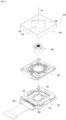
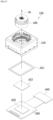
- FIG. 1 is a perspective view of a camera device 200 according to an embodiment
- FIG. 2 is an exploded perspective view of the camera device 200 shown in FIG. 1
- FIG. 3A is a cross-sectional view taken along line AB in FIG. 1
- FIG. 3B is a cross-sectional view taken along line CD in FIG. 1
- FIG. 3C is a cross-sectional view taken along line EF in FIG. 1
- FIG. 4 is an exploded perspective view of an AF moving unit 100 shown in FIG. 2
- FIG. 5 is a perspective view of a bobbin 110, a sensing magnet 180, a balancing magnet 185, a coil 120, a circuit board 190, and a first position sensor 170 shown in FIG. 4
- FIG. 5 is a perspective view of a bobbin 110, a sensing magnet 180, a balancing magnet 185, a coil 120, a circuit board 190, and a first position sensor 170 shown in FIG. 4
- FIG. 6 is a perspective view of the bobbin 100, a housing 140, the circuit board 190, and an upper elastic member 150
- FIG. 7 is a bottom perspective view of the housing 140, the bobbin 110, a lower elastic member 160, a magnet 130, and the circuit board 190.
- the camera device 200 may include an AF moving unit 100 and an image sensor unit 350.
- the camera device 200 may further include at least one of a cover member 300, a lens module 400, or a lower base 219.
- the cover member 300 and the lower base 219 may constitute a case.
- the AF moving unit 100 may be coupled to the lens module 400, and may move the lens module in the optical-axis (OA) direction or a direction parallel to the optical axis.
- the autofocus function of the camera device 200 may be performed by the AF moving unit 100.
- the image sensor unit 350 may include an image sensor 810.
- the image sensor unit 350 may move the image sensor 810 in a direction perpendicular to the optical axis, or may tilt or rotate the image sensor 810 to a predetermined angle with respect to the optical axis.
- the image sensor unit 350 may include a shape memory alloy member 45, which interconnects an OIS moving unit and a fixed unit.
- the optical image stabilization function of the camera device 200 may be performed by the image sensor unit 350.
- the image sensor 810 may be rotated about at least one of the x-axis, the y-axis, or the z-axis.
- the image sensor 810 may be moved in at least one of the x-axis direction, the y-axis direction, or the z-axis direction.
- the image sensor 810 may be tilted about at least one of the x-axis, the y-axis, or the z-axis.
- the AF moving unit 100 may alternatively be referred to as a "lens moving unit” or a “lens driving apparatus.” Alternatively, the AF moving unit 100 may be referred to as a "first actuator” or an "AF driving unit.”
- the lens module 400 is not moved in a direction perpendicular to the optical axis, but the image sensor 810 may be moved in a direction perpendicular to the optical axis by the image sensor unit 350.
- OIS optical image stabilization
- the image sensor unit 350 may alternatively be referred to as an "image sensor moving unit,” an “image sensor shift unit,” a “sensor driving unit,” or a “sensor shift unit.”
- the image sensor unit 350 may be referred to as a “second actuator” or an "OIS driving unit.”
- the AF moving unit 100 may include a bobbin 110, a coil 120, a magnet 130, and a housing 140.
- the AF moving unit 100 may further include an upper elastic member 150 and a lower elastic member 160.
- the AF moving unit 100 may include a first position sensor 170, a circuit board 190, and a sensing magnet 180 in order to implement AF feedback.
- the AF moving unit 100 may further include a balancing magnet 185.
- the bobbin 110 may be disposed in the housing 140, and may be moved in the optical-axis (OA) direction or the first direction (e.g. the Z-axis direction) by electromagnetic interaction between the coil 120 and the magnet 130.
- OA optical-axis
- first direction e.g. the Z-axis direction
- the bobbin 110 may have a bore 110A formed therein in order to be coupled to the lens module 400 or to mount the lens module 400 therein.
- the bore 110A in the bobbin 110 may be a through-hole formed through the bobbin 110 in the optical-axis direction, and may have a circular shape, an elliptical shape, or a polygonal shape, without being limited thereto.
- the lens module 400 may include at least one lens and/or a lens barrel.
- the lens module 400 may include one or more lenses and a lens barrel accommodating the one or more lenses.
- the disclosure is not limited thereto. Any of various holding structures may be used in place of the lens barrel, so long as the same is capable of supporting one or more lenses.
- the lens module 400 may be screwed to the bobbin 110.
- the lens module 400 may be coupled to the bobbin 110 by means of an adhesive (not shown).
- the light that has passed through the lens module 400 may pass through a filter 610, and may be introduced into the image sensor 810.
- the bobbin 110 may include a protruding portion 111 formed on the outer surface thereof.
- the protruding portion 111 may protrude in a direction parallel to a line perpendicular to the optical axis OA.
- the disclosure is not limited thereto.
- the protruding portion 111 of the bobbin 110 may correspond to a recess portion 25a in the housing 140, and may be inserted into or disposed in the recess portion 25a in the housing 140.
- the protruding portion 111 may suppress or prevent the bobbin 110 from rotating beyond a predetermined range about the optical axis.
- the protruding portion 111 may serve as a stopper for preventing the bobbin 110 from moving beyond a predetermined range in the optical-axis direction (e.g. a direction from the upper elastic member 150 toward the lower elastic member 160) due to external impact or the like.
- the bobbin 110 may have a first escape recess 112a formed in the upper surface thereof to avoid spatial interference with a first frame connection portion 153 of the upper elastic member 150.
- the bobbin 110 may have a second escape recess 112b formed in the lower surface thereof to avoid spatial interference with a second frame connection portion 163 of the lower elastic member 160.
- the bobbin 110 may include a first coupling portion 116a in order to be coupled or secured to the upper elastic member 150.
- the first coupling portion of the bobbin 110 may take the form of a flat surface, but the disclosure is not limited thereto.
- the first coupling portion may take the form of a protrusion or a recess.
- the bobbin 110 may include a second coupling portion 116b in order to be coupled or secured to the lower elastic member 160.
- the second coupling portion 116b may take the form of a flat surface, but the disclosure is not limited thereto.
- the second coupling portion 116b may take the form of a protrusion or a recess.
- the bobbin 110 may have a recess formed in the outer surface thereof to allow the coil 120 to be seated therein, inserted thereinto, or disposed therein.
- the recess in the bobbin 110 may have a closed curve shape (e.g. a ring shape), which coincides with the shape of the coil 120.
- the bobbin 110 may have a first seating recess formed therein to allow the sensing magnet 180 to be seated therein, inserted thereinto, secured thereto, or disposed therein.
- the bobbin 110 may have a second seating recess formed in the outer surface thereof to allow the balancing magnet 185 to be seated therein, inserted thereinto, secured thereto, or disposed therein.
- the first and second seating recesses in the bobbin 110 may be formed in the outer surfaces of the bobbin 110 that face each other.
- the coil 120 is disposed on the bobbin 110, or is coupled to the bobbin 110.
- the coil 120 may be disposed on the outer surface of the bobbin 110.
- the coil 120 may surround the outer surface of the bobbin 110 in the direction of rotation about the optical axis OA, but the disclosure is not limited thereto.
- the coil 120 may be directly wound around the outer surface of the bobbin 110, but the disclosure is not limited thereto. In another embodiment, the coil 120 may be wound around the bobbin 110 using a coil ring, or may be embodied as a coil block having an angled ring shape.
- Power or a driving signal may be supplied to the coil 120.
- the power or the driving signal supplied to the coil 120 may be a DC signal, an AC signal, or a signal containing both DC and AC components, and may be of a voltage type or a current type.
- a driving signal e.g. a driving current
- electromagnetic force may be generated by electromagnetic interaction with the magnet 130, and the bobbin 110 may be moved in the optical-axis (OA) direction by the generated electromagnetic force.
- the bobbin 110 may be movable upwards or downwards, which is referred to as bidirectional driving of the AF driving unit.
- the bobbin 110 may be movable upwards (or forwards), which is referred to as unidirectional driving of the AF driving unit.
- the coil 120 may be disposed so as to correspond to or overlap the magnet 130, which is disposed in the housing 140, in a direction parallel to a line that is perpendicular to the optical axis OA and extends through the optical axis.
- the AF driving unit may include the bobbin 110 and components coupled to the bobbin 110 (e.g. the coil 120, the sensing magnet 180, and the balancing magnet 185).
- the AF driving unit may further include the lens module 400.
- the initial position of the AF driving unit may be the original position of the AF driving unit in the state in which no electric power is supplied to the coil 120 or the position at which the AF driving unit is located as the result of the upper and lower elastic members 150 and 160 being elastically deformed due only to the weight of the AF driving unit.
- the initial position of the bobbin 110 may be the position at which the AF driving unit is located when gravity acts in a direction from the bobbin 110 toward a base 210 or when gravity acts in a direction from the base 210 toward the bobbin 110.
- the sensing magnet 180 may provide a magnetic field, which is detected by the first position sensor 170, and the balancing magnet 185 may cancel out the influence of the magnetic field of the sensing magnet 180 and may establish weight equilibrium with the sensing magnet 180.
- the sensing magnet 180 may alternatively be referred to as a "sensor magnet.”
- the sensing magnet 180 may be disposed on the bobbin 110, or may be coupled to the bobbin 110.
- the sensing magnet 180 may be disposed so as to face the first position sensor 170.
- the balancing magnet 185 may be disposed on the bobbin 110, or may be coupled to the bobbin 110. In an example, the balancing magnet 185 may be disposed opposite the sensing magnet 180.
- each of the sensing magnet 180 and the balancing magnet 185 may be a monopolar-magnetized magnet, which has one N pole and one S pole, but the disclosure is not limited thereto.
- each of the sensing magnet 180 and the balancing magnet 185 may be a bipolar-magnetized magnet or a 4-pole magnet, which includes two N poles and two S poles.
- the sensing magnet 180 may be moved together with the bobbin 110 in the optical-axis direction, and the first position sensor 170 may detect the intensity of the magnetic field or the magnetic force of the sensing magnet 180, which is moved in the optical-axis direction, and may output an output signal corresponding to the result of the detection.
- the intensity of the magnetic field or the magnetic force detected by the first position sensor 170 may vary depending on displacement of the bobbin 110 in the optical-axis direction.
- the first position sensor 170 may output an output signal proportional to the detected intensity of the magnetic field, and the displacement of the bobbin 110 in the optical-axis direction may be detected using the output signal from the first position sensor 170.
- the housing 140 accommodates therein the bobbin 110, and supports the magnet 130, the first position sensor 170, and the circuit board 190.
- the housing 140 may be formed so as to take the overall shape of a hollow column.
- the housing 140 may have a polygonal (e.g. quadrangular or octagonal) or circular bore formed therein, and the bore in the housing 140 may take the form of a through-hole formed through the housing 140 in the optical-axis direction.
- the housing 140 may include side portions, which correspond to or face side plates 302 of the cover member 300, and corners, which correspond to or face the corners of the cover member 300.
- the housing 140 may include a stopper 145 formed on the upper portion, the upper surface, or the upper end thereof in order to be prevented from directly colliding with the inner surface of the upper plate 301 of the cover member 300.
- the housing 140 may further include a stopper protruding from the lower surface thereof.
- the stopper 145 may alternatively be referred to as a "boss” or a "protrusion.”
- the housing 140 may have a mounting groove (or a seating groove) 14a formed therein to accommodate the circuit board 190.
- the mounting groove 14a may have a shape coinciding with the shape of the circuit board 190.
- the housing 140 may have an opening 141 formed therein to expose terminals B 1 to B4 of a terminal unit 95 of the circuit board 190 therethrough.
- the opening 141 may be formed in the side portion of the housing 140.
- the housing 140 may be provided on the upper portion, the upper end, or the upper surface thereof with at least one first coupling portion for coupling to a first outer frame 152 of the upper elastic member 150.
- the housing 140 may be provided on the lower portion, the lower end, or the lower surface thereof with a second coupling portion for coupling and securing to a second outer frame 162 of the lower elastic member 160.
- each of the first and second coupling portions of the housing 140 may be formed in the shape of a protrusion, a recess, or a flat surface.
- the housing 140 may be coupled to a lower base 219 to be described later.
- the lower portion, the lower end, or the lower surface of the housing 140 may be coupled to the upper portion, the upper end, or the upper surface of the lower base 219.
- the magnet 130 may be disposed in the housing 140. In an example, the magnet 130 may be disposed on the side portion of the housing 140.
- the magnet 130 may be an AF driving magnet for implementing AF operation.
- the magnet 130 may include two or more magnets that correspond to or face the coil 120.
- the magnet 130 may include magnets 130-1 to 130-4, which are disposed on the side portions of the housing 140. In another embodiment, the magnet 130 may include two magnets disposed on two opposite side portions of the housing 140. In still another embodiment, the magnet 130 may be disposed on a corner of the housing 140.
- the magnet 130 may be disposed in the housing 140 such that at least a portion thereof overlaps the coil 120 in a direction parallel to a line that is perpendicular to the optical axis OA and extends through the optical axis OA.
- Each of the first to fourth magnets 130-1 to 130-4 may be a monopolar-magnetized magnet, but the disclosure is not limited thereto. In another embodiment, each of the first to fourth magnets 130-1 to 130-4 may be a bipolar-magnetized magnet or a 4-pole magnet, which includes two N poles and two S poles.
- the coil 120 is disposed on the bobbin, and the magnet 130 is disposed in the housing.
- the coil may be disposed in the housing 140, and the magnet may be disposed on the bobbin.
- the circuit board 190 may be disposed in the housing 140, and the first position sensor 170 may be disposed or mounted on the circuit board 190.
- the circuit board 190 may be disposed in the mounting groove 14a in the housing 140, and the terminals of the circuit board 190 may be exposed to the outside of the housing 140 through the opening 141 in the housing 140.
- the circuit board 190 may include a terminal part (or a terminal unit) 95 including a plurality of terminals B1 to B4 in order to be conductively connected to an external terminal or an external device, and the plurality of terminals B1 to B4 may be conductively connected to the first position sensor 170.
- the first position sensor 170 may be disposed on a first surface of the circuit board 190, and the plurality of terminals B 1 to B4 may be disposed on a second surface of the circuit board 190.
- the second surface of the circuit board 190 may be a surface opposite the first surface of the circuit board 190.
- the first surface of the circuit board 190 may be a surface of the circuit board 190, which faces the bobbin 110 or the sensing magnet 180.
- the circuit board 190 may be a printed circuit board or an FPCB.
- the circuit board 190 may include a circuit pattern or a wiring (not shown) for conductively connecting the first to fourth terminals B 1 to B4 to the first position sensor 170.
- the first position sensor 170 may detect the magnetic field or the intensity of the magnetic field of the sensing magnet 180 mounted to the bobbin 110, and may output an output signal corresponding to the result of the detection.
- the first position sensor 170 may take the form of a driver IC including a Hall sensor.
- the first position sensor 170 may include a Hall sensor and a driver.
- the first position sensor 170 may include first to fourth terminals for transmitting and receiving data to and from the outside through data communication using a protocol, for example, I2C communication, and fifth and sixth terminals for directly providing a driving signal to the coil 120.
- the first to fourth terminals of the first position sensor 170 may be conductively connected to the first to fourth terminals B1 to B4 of the circuit board 190.
- the fifth and sixth terminals of the first position sensor 170 may be conductively connected to the coil 120 through at least one of the upper elastic member 150 or the lower elastic member 160, and may provide a driving signal to the coil 120.
- the fifth and sixth terminals of the first position sensor 170 may be conductively connected to the first and second elastic members 150-1 and 150-2, may be conductively connected to the coil 120, and may provide a driving signal to the coil 120.
- the first position sensor 170 may be implemented as a Hall sensor alone.
- the first position sensor 170 may include two input terminals for receiving a driving signal or power and two output terminals for outputting a sensing voltage (or an output voltage).
- the circuit board 190 may include first to fourth terminals B1 to B4 conductively connected to the first position sensor 170 and fifth and sixth terminals (not shown) conductively connected to the coil 120.
- driving power may be provided to the first position sensor 170 through the first and second terminals B 1 and B2 of the circuit board 190, and the output of the first position sensor 170 may be output to the outside through the third and fourth terminals B3 and B4.
- the fifth and sixth terminals of the circuit board 190 may be conductively connected to at least one of the upper elastic member 150 or the lower elastic member 160, and may provide a driving signal to the coil 120.
- the fifth and sixth terminals of the circuit board 190 may be conductively connected to the first and second elastic members 150-1 and 150-2 of the upper elastic member 150, and may provide a driving signal to the coil 120 through the first and second elastic members 150-1 and 150-2.
- the camera device may further include a capacitor 195, which is disposed on the circuit board 190.
- the capacitor may be of a chip type.
- the capacitor 195 may be conductively connected in parallel to the first and second terminals B1 and B2 of the circuit board 190 for providing power (or a driving signal) to the position sensor 170 from the outside.
- the capacitor 195 may be conductively connected in parallel to the terminals of the first position sensor 170 conductively connected to the first and second terminals B1 and B2 of the circuit board 190.
- the capacitor 195 may serve as a smoothing circuit for removing ripple components included in power signals GND and VDD provided to the first position sensor 170 from the outside, and thus may provide stable and consistent power signals to the first position sensor 170.
- the upper elastic member 150 may be coupled to the upper portion, the upper end, or the upper surface of the bobbin 110 and to the upper portion, the upper end, or the upper surface of the housing 140
- the lower elastic member 160 may be coupled to the lower portion, the lower end, or the lower surface of the bobbin 110 and to the lower portion, the lower end, or the lower surface of the housing 140.
- the upper elastic member 150 and the lower elastic member 160 may elastically support the bobbin 110 with respect to the housing 140.
- the upper elastic member 150 may include first and second elastic members 150-1 and 150-2.
- the lower elastic member 160 is illustrated in FIG. 7 as being formed as a single unit or a single component, the disclosure is not limited thereto.
- At least one of the upper elastic member or the lower elastic member may include a plurality of elastic units or springs, which are conductively isolated or spaced apart from each other.
- the upper elastic member 150 may further include a first inner frame 151, which is coupled or secured to the upper portion, the upper surface, or the upper end of the bobbin 110, a second inner frame 152, which is coupled or secured to the upper portion, the upper surface, or the upper end of the housing 140, and a first frame connection portion 153, which connects the first inner frame 151 to the first outer frame 152.
- the lower elastic member 160 may include a second inner frame 161, which is coupled or secured to the lower portion, the lower surface, or the lower end of the bobbin 110, second outer frames 162-1 to 162-3, which are coupled or secured to the lower portion, the lower surface, or the lower end of the housing 140, and a second frame connection portion 163, which connects the second inner frame 161 to the second outer frames 162-1 to 162-3.
- Each of the first and second frame connection portions 153 and 163 may be bent or curved at least once so as to form a pattern having a predetermined shape.
- Each of the upper elastic member 150 and the lower elastic member 160 may be formed of a conductive material.
- the circuit board 190 may include two pads 5a and 5b.
- the first pad 5a may be located on the second surface of the circuit board 190
- the second pad 5b may be located on the first surface of the circuit board 190, but the disclosure is not limited thereto.
- the first and second pads may be formed on any one of the first surface and the second surface of the circuit board 190.
- the first and second pads 5a and 5b may be conductively connected to the fifth and sixth terminals of the position sensor 170.
- the first pad 5a may be coupled to the first elastic member 150-1
- the second pad 5b may be coupled to the second elastic member 150-2.
- the first outer frame of the first elastic member 150-1 may include a first coupling portion 4a coupled to the first pad 5a
- the first outer frame of the second elastic member 150-2 may include a second coupling portion 4b coupled to the second pad 5b.
- one end of the coil 120 may be coupled to the first elastic member 150-1, and the other end of the coil 120 may be coupled to the second elastic member 150-2.
- the upper elastic member may be coupled to the first pad of the circuit board 190 so as to be conductively connected thereto, and the lower elastic member may be coupled to the second pad of the circuit board 190 so as to be conductively connected thereto.
- the lower elastic member may include two lower elastic members. Each of the two lower elastic members may be coupled or conductively connected to a corresponding one of the first and second pads of the circuit board 190, and the coil 120 may be conductively connected to the two lower elastic members.
- the first and second pads 5a and 5b may be conductively connected to the fifth and sixth terminals of the circuit board 190, rather than being conductively connected to the position sensor 170.
- the sensing magnet is disposed on the bobbin, and the position sensor is disposed in the housing.
- the disclosure is not limited thereto.
- the sensing magnet may be disposed in the housing, and the position sensor may be disposed on the bobbin so as to correspond to or face the sensing magnet.
- the sensing magnet may be disposed on the bobbin, and the position sensor may be disposed on the base 210 so as to correspond to or face the sensing magnet in the optical-axis direction.
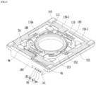
- FIG. 8 is a perspective view of the image sensor unit 350
- FIG. 9A is an upper perspective view of the base 210
- FIG. 9B is a lower perspective view of the base 210
- FIG. 10 is a view showing coupling of the AF moving unit 100 and the base 210
- FIG. 11 is an exploded perspective view of the image sensor unit 350 shown in FIG. 8
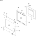
- FIG. 12 is a first exploded perspective view of a first board unit 305
- FIG. 13 is a second exploded perspective view of the first board unit 305.
- the image sensor unit 350 may include a fixed unit, an OIS moving unit, which is disposed so as to be spaced apart from the fixed unit, an elastic member (or an elastic support member), which is connected to the fixed unit and the OIS moving unit and supports the OIS moving unit with respect to the fixed unit, and a shape memory alloy member 45, which causes the OIS moving unit to move in a direction perpendicular to the optical axis.
- the fixed unit may include at least one of the housing 140, the base 210, the second board unit 800, or the lower base 219.
- the OIS moving unit may include a first board unit 350 and components disposed on the first board unit 305.
- the OIS moving unit may further include at least one of the image sensor 810, the filter 600, a filter holder 600, or a controller 830.
- the elastic member may include at least one of a first elastic member 310 or a second elastic member 320.
- the elastic members 310 and 320 may elastically support the OIS moving unit with respect to the fixed unit.
- the elastic members 310 and 320 may alternatively be referred to as "support members” or "elastic parts.”
- the first elastic member 310 may conductively connect the shape memory alloy member 45 to the first board unit 305
- the second elastic member 320 may conductively connect the first board unit 305 to the second board unit 800.
- the shape memory alloy member 45 may be plated with at least one of gold or tin. Thereby, it may also be possible to suppress corrosion of the shape memory alloy member 45.
- the image sensor unit 350 may include the base 210, the first elastic member 310, the first board unit 305, the image sensor 810 disposed on the first board unit, and the shape memory alloy member 45.
- the image sensor unit 350 may further include the second board unit 800 and the second elastic member 320.
- the first elastic member 310 and the second elastic member 320 may be wrapped with an insulative material or sealed in order to prevent electrical short circuit and corrosion.
- the base 210 may be disposed under the housing 140 of the AF moving unit, and may be coupled to the housing 140.
- the base 210 may be disposed on the first board unit 305, e.g. the upper surface of the first circuit board 250.
- the base 210 may correspond to the fixed unit.
- the base 210 may serve to couple the AF fixed unit (e.g. the housing 140) of the AF moving unit to the OIS fixed unit (e.g. the lower base 219).
- the base 210 may be coupled to the OIS fixed unit, and may be supported by the OIS fixed unit.
- the base 210 may include at least one of plastic, resin, or metal.
- the base 210 may have formed therein a bore 210A, which corresponds to or faces the image sensor 810.
- the bore 210A may be a through-hole formed through the base 210 in the optical-axis direction.
- the bore 210A may have a polygonal shape, e.g. a quadrangular shape or an octagonal shape.
- the disclosure is not limited thereto, and the bore 210A may have a circular shape or an elliptical shape.
- the outer circumferential surface of the base 210 may have a polygonal shape, e.g. a quadrangular shape, a pentagonal shape, or a hexagonal shape. However, the disclosure is not limited thereto. In another embodiment, the outer circumferential surface of the base 210 may have a circular shape or an elliptical shape.
- the base 210 may include at least one protruding portion (or protrusion) 224 protruding from the upper surface thereof.
- the at least one protruding portion 224 may be in contact with, attached to, or coupled to the lower portion, the lower end, or the lower surface of the housing 140 of the AF moving unit by means of an adhesive.
- the base 210 may include a plurality of protruding portions 22A to 22D, which are spaced apart from each other.
- the plurality of protruding portions 22A to 22D may be disposed corresponding to sides of the upper surface of the base 210.
- the base 210 may include a coupling portion 216, which is coupled to the first elastic member 310.
- the coupling portion 216 may protrude from the lower surface of the base 210.
- the coupling portion 216 may alternatively be referred to as a "protruding portion,” a "protrusion,” or a "column portion.”
- the coupling portion 216 may include a first coupling portion 216A, which is disposed on a first corner of the lower surface of the base 210, and a second coupling portion 216B, which is disposed on a second corner of the lower surface of the base 210.
- the first corner of the base 210 may face the second corner in a first diagonal direction.
- the base 210 may have escape recesses 212 formed therein to avoid spatial interference with support portions 217 disposed on the first board unit 305.
- the escape recesses 212 may be formed on a third corner and a fourth corner of the base 210, and the third corner may face the fourth corner in a second diagonal direction. The first diagonal direction and the second diagonal direction may be perpendicular to each other.
- the base 210 may include at least one protrusion 214 protruding from the lower surface thereof.
- the number of protrusions 214 may be two or greater.
- the at least one protrusion 214 may serve to maintain an air gap formed between the lower surface of the base 210 and the first board unit 305.
- the at least one protrusion 214 may serve as a stopper for preventing the lower surface of the base 210 from directly colliding with the first board unit 305.
- the protrusion 214 may be in contact with the first board unit 305, e.g. a first surface 31A of the first circuit board 250.
- the lower surface of the protrusion 214 may be located below the lower surface of the coupling portion 216.
- the length by which the protrusion 214 protrudes may be longer than the length by which the coupling portion 216 protrudes.
- the base 210 may be spaced apart from the first board unit 305. In an example, the lower surface of the base 210 may be spaced apart from the upper surface of the first board unit 305.
- the first board unit 305 may be disposed below the base 210.
- the first board unit 305 may include a board on which the image sensor 810 is disposed, and may alternatively be referred to as a first board, a first circuit board, a moving circuit board, a main circuit board, a main board, or a moving board.
- the lens module 400 may be disposed on the first board unit 305. In an example, the lens module 400 may be located on the filter 610 disposed on the filter holder 600.
- the first board unit 305 may include at least one board on which the image sensor 810 is disposed.
- the first board unit 305 may include one or more pads Q1 and Q2, which are coupled to the first elastic member 310.
- the one or more pads Q1 and Q2 may be conductively connected to the first elastic member 310.
- the first board unit 305 may include one or more pads (or terminals) P1 to P4, which are conductively connected to the shape memory alloy member 45.
- the first board unit 305 may include at least one pad (or terminal) 261, which is coupled to the second elastic member 320, and the at least one pad 261 may be conductively connected to the second elastic member 320.
- the first board unit 305 may include a first circuit board 250, a second circuit board 260 disposed under the first circuit board 250, and a third circuit board 270 disposed under the second circuit board 260.
- the first circuit board 250 may include a bore 250A formed therein so as to correspond to or face the bore 101 in the bobbin 110, the bore in the housing 450, and/or the lens module 400.
- the bore 250A may be a through-hole formed through the first circuit board 250 in the optical-axis direction, and may be formed in the center of the first circuit board 250.
- the first circuit board 250 e.g. the outer periphery thereof, may have a polygonal shape, e.g. a quadrangular shape, but the disclosure is not limited thereto.
- the bore 250A in the first circuit board 250 may have a polygonal shape, e.g. a quadrangular shape, a circular shape, or an elliptical shape, but the disclosure is not limited thereto.
- the controller 830 may be disposed on the first surface 31A of the first circuit board 250, but the disclosure is not limited thereto.
- the one or more pads Q1 and Q2, which are coupled to the first elastic member 310, may be formed on the first surface 31A of the first circuit board 250.
- the pads Q1 and Q2 may alternatively be referred to as terminals, coupling portions, conductive patterns, or conductive layers.
- a first pad Q1 and a second pad Q2, to which two second coupling portions 312 and 322 of the first elastic member 310 are coupled may be formed on the first surface of the first circuit board 250.
- the one or more pads P1 to P4, which are conductively connected to the shape memory alloy member 45, may be formed on the first surface 31A of the first circuit board 250.
- At least one pad 251, which is conductively connected to the second circuit board 260, may be formed on a second surface 31B of the first circuit board 250.
- the first circuit board 250 may include a plurality of pads 251, which are disposed around the bore 250A.
- the first surface 31A of the first circuit board 250 may be a surface that faces the base 210, and the second surface 31B of the first circuit board 250 may be a surface opposite the first surface of the first circuit board 250.
- the second circuit board 260 may include a bore 260A formed therein so as to correspond to or face the bore 250A in the first circuit board 250.
- the bore 260A may be a through-hole formed through the second circuit board 260 in the optical-axis direction, and may be formed in the center of the second circuit board 260.
- the bore 260A in the second circuit board 260 may have the same size as the bore 250A in the first circuit board 250, but the disclosure is not limited thereto. In another embodiment, the former may be larger or smaller than the latter.
- the second circuit board 260 e.g. the outer periphery thereof, may have a polygonal shape, e.g. a quadrangular shape, but the disclosure is not limited thereto.
- the bore 260A in the second circuit board 260 may have a polygonal shape, e.g. a quadrangular shape, a circular shape, or an elliptical shape, but the disclosure is not limited thereto.
- At least one first pad 261, which is conductively connected to the first circuit board 250 may be formed on a first surface 32A of the second circuit board 260.
- the first surface 32A of the second circuit board 260 may be a surface facing the second surface 31B of the first circuit board 250.
- the pad 251 of the first circuit board 250 and the first pad 261 of the second circuit board 260 may be coupled to each other by means of a conductive adhesive or a solder.
- the second circuit board 260 may include a plurality of first pads 261, which are disposed adjacent to the bore 260A.
- the first pads 261 may be disposed between a first side of the first surface 32A and the bore 260A and between a second side of the first surface 32A and the bore 260A.
- the first side and the second side of the first surface may face each other or may be located opposite each other.
- At least one second pad 262, which is conductively connected to the third circuit board 270, may be formed on a second surface 32B of the second circuit board 260.
- the second surface 32B of the second circuit board 260 may be a surface opposite the first surface 32A of the second circuit board 260.
- the second circuit board 260 may include a plurality of second pads 262, which are disposed on the second surface 32B at positions adjacent to the bore 260A.
- the second pads 262 may be disposed between a first side of the second surface 32B and the bore 260A and between a second side of the second surface 32B and the bore 260A.
- the first side and the second side of the second surface 32B may face each other or may be located opposite each other.
- At least one third pad 263, which is coupled to the second elastic member 320, may be formed on the second surface 32B of the second circuit board 260.
- the second circuit board 260 may include a plurality of third pads 263, which are disposed on the second surface 32B at positions adjacent to the bore 260A.
- the third pads 263 may be disposed between a third side of the second surface 32B and the bore 260A and between a fourth side of the second surface 32B and the bore 260A.
- the third side and the fourth side of the second surface 32B may face each other or may be located opposite each other, and may be perpendicular to the first side (or second side).
- the second circuit board 260 may include at least one protruding portion 265, which protrudes from a side surface thereof in a direction perpendicular to the optical axis.
- the protruding portion 265 functions to increase the contact area between the second circuit board 260 and the first circuit board 250 to increase coupling force therebetween.
- At least one pad 271, which is conductively connected to the second pad 262 of the second circuit board 260, may be formed on a first surface 33A of the third circuit board 270.
- the first surface 33A of the third circuit board 270 may be a surface that faces or is opposite the second surface 32B of the second circuit board 260.
- the third circuit board 270 may include a plurality of pads 271, and the plurality of pads 271 may be disposed around the image sensor 810.
- the second pad 262 of the second circuit board 260 and the pad 271 of the third circuit board 270 may be coupled and conductively connected to each other by means of a conductive adhesive or a solder.
- the image sensor 810 may be disposed on the first surface 33A of the third circuit board 270.
- the area of the bore 260A in the second circuit board 260 may be larger than that of the image sensor 810.
- the filter holder 600, the filter 610, and the image sensor 810 may be disposed in the bore 250A in the first circuit board 250 and the bore 260 in the second circuit board 260.
- the first circuit board 250 may be a main board on which various elements (e.g. the controller 830) are mounted
- the third circuit board 270 may be a board on which the image sensor 810 is mounted, and may be conductively connected to the image sensor 810 via a plurality of conductive members (e.g. wires).
- the second circuit board 260 may be conductively connected to the first circuit board 250 and the third circuit board 270, and may be conductively connected to the second board unit 800 via the second elastic member 320.
- Each of the first to third circuit boards 250, 260, and 270 may include at least one of a printed circuit board or a flexible printed circuit board (FPCB).
- FPCB flexible printed circuit board
- first board unit 305 is illustrated in FIGs. 12 and 13 as including three circuit boards, the disclosure is not limited thereto. In another embodiment, at least two of the first to third circuit boards 250, 260, and 270 may be combined into a single board.
- the second board unit 800 may be spaced apart from the first board unit 305. In an example, the second board unit 800 may be located below the first board unit 305.
- the first board unit 305 may be disposed in the bore 800A in the second board unit 800.
- a portion of the third circuit board 270 may be disposed in the bore 800A in the second board unit 800.
- the second surface 32B of the second circuit board 260 may be positioned at the same height as or higher than the upper surface of the second board unit 800.
- the second board unit 800 may serve to provide a signal from the outside to the image sensor unit 350 or to output a signal from the image sensor unit 350 to the outside.
- the second board unit 800 may alternatively be referred to as a second board, a second circuit board, a fixed circuit board, a sub-circuit board, a sub-board, or a fixed board.
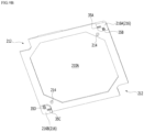
- FIG. 14 is a bottom view of the first elastic member 310, the base 210, and the shape memory alloy member 45
- FIG. 15 is a view for explaining the coupling relationship between the first elastic member 310 and the first board unit 305
- FIG. 16 is a plan view of the second board unit 800
- FIG. 17 is a plan view of the second elastic member 320
- FIG. 18 is a view showing coupling between the second board unit 800 and the second elastic member 320
- FIG. 19 is a view showing coupling between the second circuit board 260 of the first board unit 800 and the second elastic member 320
- FIG. 20 is a view showing coupling between an insulation member and the second elastic member 320
- FIG. 21 is a cross-sectional view taken along line GH in FIG. 8
- FIG. 22 is a cross-sectional view taken along line IJ in FIG. 8 .
- the second board unit 800 may include a first region 801 corresponding to the AF moving unit 100, a second region 802 in which a connector 840 is disposed, and a third region 803 interconnecting the first region 801 and the second region 802.
- the third region 803 may serve as an interposer interconnecting the first region 801 and the second region 802.
- the connector 840 may be conductively connected to the second region 802 of the second board unit 800, and may include a port in order to be conductively connected to an external device.
- Each of the first region 801 and the second region 802 of the second board unit 800 may include a flexible substrate and a rigid substrate, and the third region 803 thereof may include a flexible substrate, but the disclosure is not limited thereto.
- at least one of the first to third regions 801 to 803 of the circuit board 800 may include at least one of a rigid substrate or a flexible substrate.
- the first region 801 may alternatively be referred to as a "first substrate,” the second region 802 may alternatively be referred to as a "second substrate,” and the third region 803 may alternatively be referred to as a "third substrate.”
- the second board unit 800 may have formed therein a bore 800A corresponding to the bore 101 in the bobbin 110 of the AF moving unit 100, the lens module 400, and/or the image sensor 810, or the first board unit 305.
- the bore 800A may be a through-hole formed through the second board unit 800 in the optical-axis direction.
- the bore 800A in the second board unit 800 may be formed in the first region 801.
- the first region 801 of the second board unit 800 may have a polygonal shape (e.g. a quadrangular shape, a square shape, or a rectangular shape), but the disclosure is not limited thereto.
- the first region of the second board unit may have a circular shape.
- the bore 800A in the second board unit 800 may have a polygonal shape (e.g. a quadrangular shape, a square shape, or a rectangular shape), but the disclosure is not limited thereto.
- the bore in the second board unit may have a circular shape.
- the second board unit 800 may include at least one pad 801, which is conductively connected to the second elastic member 320.
- the at least one pad 801 of the second board unit 800 may include a plurality of pads A1 to An (where n is a natural number greater than 1 (n>1)).
- the pad 801 may alternatively be referred to as a "lead pattern,” a "terminal,” or a "lead member.”
- each of the plurality of pads A1 to An may correspond to, face, or overlap springs R1 to Rn (where n is a natural number greater than 1 (n>1)) in the optical-axis (OA) direction.
- the plurality of pads A1 to An may be disposed around the bore 800A in the second board unit 800.
- the plurality of pads A1 to An may be disposed adjacent to the bore 800A in the second board unit 800, and may be spaced apart from each other.
- the plurality of pads 800B may be disposed in a region between the bore 800A in the second board unit 800 and sides of the second board unit 800.
- the second board unit 800 may include at least one terminal, which is conductively connected to the circuit board 190 of the AF moving unit.
- the second board unit may include a plurality of terminals K1 to K4.
- the first position sensor 170 may perform data communication with the outside through the second board unit 800.
- the plurality of terminals K1 to K4 may be formed on the first surface of the second board unit 800. In an example, the plurality of terminals K1 to K4 may be disposed adjacent to one corner of the first region of the second board unit 800.
- Each of the plurality of terminals K1 to K4 may be conductively connected to a corresponding one of the terminals B1 to B4 of the circuit board 190 by means of a conductive adhesive member or a solder.
- the second board unit 800 may include a connector 840, which is disposed in the second region 802.
- the connector 840 may be disposed on one surface (e.g. the lower surface or the upper surface) of the second region 802 of the second board unit 800.
- the image sensor unit 350 may include a motion sensor 820 and a controller 830.
- the image sensor unit may include at least one of a memory (not shown) or a capacitor.
- the motion sensor 820, the controller 830, the memory, and the capacitor may be disposed or mounted on any one of the first board unit 305 and the second board unit 800.
- the motion sensor 820 may be disposed on the second board unit 800, and the controller 830 may be disposed on the first board unit 305.
- the motion sensor 820 disposed on the second board unit 800 may be conductively connected to the controller 830 disposed on the first board unit 305 via the second elastic member 320.
- the motion sensor 820 outputs information about a rotational angular speed in response to movement of the camera device 200.
- the motion sensor 820 may be implemented as a 2-axis, 3-axis, or 5-axis gyro sensor or an angular speed sensor.
- the memory may store first code values corresponding to displacement of the bobbin 110 in the optical-axis direction in order to perform AF feedback.
- the memory may store second code values corresponding to displacement of the OIS moving unit in a direction perpendicular to the optical axis in order to perform OIS feedback.
- the memory may store an algorithm or a program for operation of the controller 830.
- the first code values and the second code values may be stored in a memory 760 of the optical instrument 200A.
- the memory may be a non-volatile memory such as an electrically erasable programmable read-only memory (EEPROM), but the disclosure is not limited thereto.
- EEPROM electrically erasable programmable read-only memory
- the controller 830 may be conductively connected to the first position sensor 170 and/or the second position sensor 240.
- the first circuit board 250 may be provided with an AF controller (or a driver IC) configured to receive an output of the first position sensor 170.
- the controller 780 of the optical instrument 200A may receive an output signal of the first position sensor 170 from the AF controller, may receive the first code values from the memory, and may control a driving signal, which is to be provided to the coil 120, using the received output of the first position sensor 170 and the received first code values, whereby feedback autofocus operation may be performed.
- the AF controller may control a driving signal, which is to be provided to the coil 120, using the output of the first position sensor 170 and the first code values.
- the first position sensor 170 may transmit an output of the first position sensor 170 to the controller 780 of the optical instrument 200A using I2C communication, and the controller 780 of the optical instrument 200A may control a driving signal, which is to be provided to the coil 120, using the output of the first position sensor 170 and the first code values stored in the memory, whereby feedback autofocus operation may be performed.
- the controller 780 may control a driving signal, which is to be provided to the coil 120, using the output of the first position sensor 170 and the first code values stored in the memory.
- the controller 830 may be implemented in the form of a driver IC, but the disclosure is not limited thereto.
- the controller 830 may be conductively connected to the pads 251 of the first circuit board 250 of the first board unit 305, and may be conductively connected to the second pads 262 of the second circuit board 260 of the first board unit 305.
- the first elastic member 310 may interconnect the base 210, which is the fixed unit, and the first board unit 305, which is the OIS moving unit.
- the first elastic member 310 may be disposed under the base 210.
- One end of the first elastic member 310 may be coupled to the base 210, and the other end of the second elastic member 310 may be coupled to the first board unit 305 (e.g. the first circuit board 250).
- the first elastic member 310 may include first coupling portions 311 and 321, which are coupled to the base 210, second coupling portions 312 and 322, which are coupled to the first board unit 305, and connection portions 313 and 323, which interconnect the first coupling portions 311 and 321 and the second coupling portions 312 and 322.
- the first coupling portions 311 and 321 may alternatively be referred to as “outer portions,” “outer frames,” or “first portions”
- the second coupling portions 312 and 322 may alternatively be referred to as “inner portions,” “inner frames,” or “second portions”
- the connection portions 313 and 323 may alternatively be referred to as connection frames or "third portions.”
- the first coupling portions 311 and 321 may be coupled to the first corner and the second corner of the base 210. In an example, the first coupling portions 311 and 321 may be coupled to the coupling portion 216 of the base 210. In an example, the first coupling portions 311 and 321 may at least partially be disposed within the coupling portion 216 of the base 210. In an example, the first coupling portions 311 and 321 may be located between the upper surface of the base 210 and the lower surface of the coupling portion 216 of the base 210.
- the first coupling portions 311 and 321 of the first elastic member 310 may include a 1-1 st coupling portion 311, which is coupled to the first coupling portion 216A of the base 210, and a 1-2 nd coupling portion 321, which is coupled to the second coupling portion 216B of the base 210.
- the second coupling portions 312 and 322 of the first elastic member 310 may include a 2-1 st coupling portion 312, which is coupled and conductively connected to the first board unit 305, e.g. the first pad Q1 of the first circuit board 250, and a 2-2 nd coupling portion 322, which is coupled and conductively connected to the second pad Q2.
- connection portions 313 and 323 of the first elastic member 310 may include a 1-1 st connection portion 313, which interconnects the 1-1 st coupling portion 311 and the 1-2 nd coupling portion 312, and a 1-2 nd connection portion 323, which interconnects the 2-1 st coupling portion 321 and the 2-2 nd coupling portion 322.
- connection portions 313 and 323 may be spaced apart from the base 210. In an example, the connection portions 313 and 323 may be bent or curved at least once. In an example, each of the first and second frames 314 and 324 may include at least one line portion (or straight portion) and at least one bent portion.
- the 1-1 st connection portion 313 may include a first portion, which extends from the 1-1 st coupling portion 311 disposed on the first corner of the base 210 toward the third corner of the base 210, and a second portion, which extends from the third corner of the base 210 toward the second corner of the base 210.
- the 1-1 st connection portion 313 may include a third portion interconnecting the first portion and the second portion of the 1-1 st connection portion 313, and may include a first bent portion located between the first portion and the third portion and a second bent portion located between the second portion and the third portion.
- the 1-2 nd connection portion 323 may include a first portion, which extends from the 1-2 nd coupling portion 321 disposed on the second corner of the base 210 toward the fourth corner of the base 210, and a second portion, which extends from the fourth corner of the base 210 toward the first corner of the base 210.
- the 1-2 nd connection portion 323 may include a third portion interconnecting the first portion and the second portion of the 1-2 nd connection portion 323, and may include a first bent portion located between the first portion and the third portion and a second bent portion located between the second portion and the third portion.
- the first pad Q1 of the first circuit board 250 may be located closer to the second corner of the base 210 than to the first corner, the third corner, and the fourth corner of the base 210.
- the second pad Q2 of the first circuit board 250 may be located closer to the second corner of the base 210 than to the first corner, the third corner, and the fourth corner of the base 210.
- the first pad Q1 of the first circuit board 250 may be disposed closer to the 1-2 nd coupling portion 321 than to the 1-1 st coupling portion 311, and the second pad Q2 of the first circuit board 250 may be disposed closer to the 1-1 st coupling portion 311 than to the 1-2 nd coupling portion 321.
- the length of the 1-1 st connection portion 313 and the length of the 1-2 nd connection portion 323 may be increased. If the length of the 1-1 st connection portion 313 and the length of the 1-2 nd connection portion 323 are short, elastic force supporting the OIS moving unit, e.g. the first board unit 305, is large, and thus the driving power or force of the shape memory alloy member 45 necessary to move or rotate the OIS moving unit may be increased, which may make it difficult to move or rotate the OIS moving unit using the shape memory alloy member 45.
- the first elastic member 310 may include a first frame 314, which interconnects one side of the 1-1 st coupling portion 311 and one side of the 1-2 nd coupling portion 321, and a second frame, which interconnects another side of the 1-1 st coupling portion 311 and another side of the 1-2 nd coupling portion 321.
- first frame 314 may be located outside the 1-1 st connection portion 313, and the second frame 324 may be located outside the 1-2 nd connection portion 323.
- first and second frames 314 and 324 may be included in the first coupling portions 311 and 321, and may be coupled to the base 210, but the disclosure is not limited thereto. In another embodiment, the first and second frames may be spaced apart from the base 210.
- the first and second frames 314 and 324 may be bent or curved at least once.
- each of the first and second frames 314 and 324 may include at least one line portion (or straight portion) and at least one bent portion.
- the first elastic member 310 is illustrated in FIG. 15 as including two coupling portions, the disclosure is not limited thereto. In another embodiment, the number of coupling portions may be one or three or more. In an example, the number of coupling portions of the first elastic member 310 and the number of coupling portions of the base 210 may be the same as each other.
- the first elastic member 310 may be implemented as a conductive leaf spring, but the disclosure is not limited thereto.
- the first elastic member may be implemented as a conductive and elastic member, e.g. a suspension wire or a coil spring.
- the first elastic member 310 may be formed as a single spring.
- the first elastic member may serve as a common electrode or a common ground of the shape memory alloy member 45.
- the first elastic member may include two or more springs, which are separated or spaced apart from each other.
- the camera device may include a conductive member 35, which is disposed on the base 210.
- the conductive member 35 may alternatively be referred to as a "terminal,” a "pad,” an “electrode,” or a "conductor.”
- the coupling portion 216 may include a conductive member 35, to which one end of the shape memory alloy member 45 is coupled and which is conductively connected to the first elastic member 310.
- the conductive member 35 may be disposed on the coupling portion 216 of the base 210. In an example, the conductive member 35 may pass through the coupling portion 216 of the base 210, and may be in contact with and conductively connected to the first elastic member 310.
- the conductive member 35 may include first and second conductive members 35A and 35B, which are disposed on the first coupling portion 216A of the base 210, and third and fourth conductive members 35C and 35D, which are disposed on the second coupling portion 216B.
- first and second coupling portions 216A and 216B of the base 210 may include bores or holes corresponding to the first to fourth conductive members 35A to 35D, and the first to fourth conductive members 35A to 35D may be respectively disposed in the bores or the holes in the first and second coupling portions 216A and 216B.
- first and second conductive members 35A and 35B may be connected to or integrally formed with each other. In another embodiment, the first and second conductive members 35A and 35B may be separated or spaced apart from each other.
- the third and fourth conductive members 35C and 35D may be connected to or integrally formed with each other. In another embodiment, the third and fourth conductive members 35C and 35D may be separated or spaced apart from each other.
- the first and second conductive members 35A and 35B may be coupled and conductively connected to the 1-1 st coupling portion 311 of the first elastic member 310.
- the first and second conductive members 35A and 35B may be disposed within the first coupling portion 216A of the base 210, and one end of each of the first and second conductive members 35A and 35B may be coupled and conductively connected to the 1-1 st coupling portion 311 of the first elastic member 310.
- the other ends of the first and second conductive members 35A and 35B may be exposed from the first coupling portion 216A of the base 210.
- the other ends of the first and second conductive members 35A and 35B may be exposed from the lower surface of the first coupling portion 216A of the base 210.
- the third and fourth conductive members 35C and 35D may be coupled and conductively connected to the 1-2 nd coupling portion 321 of the first elastic member 310.
- the third and fourth conductive members 35C and 35D may be disposed within the second coupling portion 216B of the base 210, and one end of each of the third and fourth conductive members 35C and 35D may be coupled and conductively connected to the 1-2 nd coupling portion 321 of the first elastic member 310.
- the other ends of the third and fourth conductive members 35C and 35D may be exposed from the second coupling portion 216B of the base 210.
- the other ends of the third and fourth conductive members 35C and 35D may be exposed from the lower surface of the second coupling portion 216B of the base 210.
- each of the first to fourth conductive members 35A to 35D may be plated with at least one of gold or tin.
- the shape memory alloy member 45 may move the OIS moving unit (or OIS driving unit) in directions perpendicular to the optical axis, e.g. the second direction (e.g. the X-axis direction) and the third direction (e.g. the Y-axis direction), due to expansion and contraction thereof.
- the shape memory alloy member 45 may rotate or tilt the OIS moving unit (or OIS driving unit) in the clockwise or counterclockwise direction with respect to the optical axis due to expansion and contraction thereof.
- the shape memory alloy member 45 may include a shape memory alloy (SMA).
- SMA shape memory alloy
- a shape memory alloy is an alloy that returns to its remembered original shape at a specific temperature when deformed.
- the shape memory alloy member 45 may be a conductive member made of a conductive material.
- the shape memory alloy member 45 may be an alloy including at least one of Ti, Ni, Cu, Fe, Au, Zn, Mn, Ag, or Cd.
- the shape memory alloy member 45 may be, for example, a wire, but the disclosure is not limited thereto. In another embodiment, the shape memory alloy member 45 may be formed in a plate shape.
- the shape memory alloy member 45 may include a first member 45A, a second member 45B, a third member 45C, and a fourth member 45D. Although the shape memory alloy member 45 is illustrated in FIG. 14 as including four independent members, the disclosure is not limited thereto. In another embodiment, the shape memory alloy member may include five or more independent members.
- the first coupling portion 216A of the base 210 may protrude from the first corner of the base 210 toward the first board unit 305, and may be coupled to the other end of the first member 45A and the other end of the fourth member 45D.
- the second coupling portion 216B of the base 210 may protrude from the second corner of the base 210 toward the first board unit 305, and may be coupled to the other end of the second member 45B and the other end of the third member 45C.
- the first circuit board 250 may include first to fourth pads corresponding to the first to fourth members 45A to 45D.
- one end of the first member 45A may be conductively connected to the first pad P1 of the first circuit board 250, and the other end of the first member 45A may be conductively connected to the first conductive member 35A disposed on the base 210.
- one end of the second member 45B may be conductively connected to the second pad P2 of the first circuit board 250, and the other end of the second member 45B may be conductively connected to the third conductive member 35C disposed on the base 210.
- one end of the third member 45C may be conductively connected to the third pad P3 of the first circuit board 250, and the other end of the third member 45C may be conductively connected to the fourth conductive member 35D disposed on the base 210.
- one end of the fourth member 45D may be conductively connected to the fourth pad P4 of the first circuit board 250, and the other end of the fourth member 45D may be conductively connected to the second conductive member 35B disposed on the base 210.
- the camera device 200 may include a support part 217, which is coupled to the first board unit 305 (e.g. the first circuit board 250) and to the shape memory alloy member 45.
- the camera device 200 may include a support part 217 (or coupling part), which is coupled to the first board unit 305 (e.g. the first circuit board 250) and to one end of each of the first to fourth members 45A to 45D.
- a support part 217 or coupling part
- the support part 217 may support one end of each of the first to fourth members 45A to 45D.
- the support part may attach, fix, or couple one end of each of the first to fourth members 45A to 45D to the first board unit 305 (e.g. the first circuit board 250).
- the lower surface of the support part 217 may be coupled or attached to the first surface 31A of the first circuit board 250 by means of an adhesive.
- the support part 217 may include a first support part 217A, which is disposed adjacent to the third corner of the base 210, and a second support part 217A, which is disposed adjacent to the fourth corner of the base 210.
- the first and second support parts 217A and 217B may be disposed adjacent to the escape recesses 212 in the base 210.
- the first and second support parts 217A and 217B may protrude from the first board unit 305, e.g. the first circuit board 250, toward the base 210.
- the first board unit 305 may include a first corner 2A, a second corner 2B, a third corner 2C, and a fourth corner 2D.
- the first corner 2A and the second corner 2B may face each other or may be located opposite each other in the first diagonal direction
- the third corner 2C and the fourth corner 2D may face each other or may be located opposite each other in the second diagonal direction.
- the first diagonal direction and the second diagonal direction may be perpendicular to each other.
- the first coupling portion 216A of the base 210 may be disposed so as to correspond to, face, or overlap the first board unit 305, e.g. the first corner 2A of the first circuit board 250, and the second coupling portion 216B of the base 210 may be disposed so as to correspond to, face, or overlap the first board unit 305, e.g. the second corner 2B of the first circuit board 250.
- first support part 217A may correspond to, face, or overlap the first board unit 305, e.g. the third corner 2C of the first circuit board 250, and may be coupled, attached, or secured to the third corner 2C.
- first support part 217A may be coupled to one end of the first member 45A and one end of the third member 45C.
- the second support part 217B may correspond to, face, or overlap the first board unit 305, e.g. the fourth corner 2D of the first circuit board 250, and may be coupled, attached, or secured to the fourth corner 2D.
- the second support part 217B may be coupled to one end of the second member 45B and one end of the fourth member 45D.
- the support part 217 may include conductive members 36A to 36D, which are coupled to the shape memory alloy member 45 and are conductively connected to the first board unit.
- the support part 217 may include conductive members 36A to 36D, which conductively connect one end of each of the first to fourth members 45A to 45D to a corresponding one of the first to fourth pads P1 to P4 of the first board unit 305 (e.g. the first circuit board 250).
- the first support part 217A may include two conductive members 36A and 36C, which are conductively separated from or independent of each other.
- One 36A of the two conductive members 36A and 36C of the first support part 217A may be conductively connected to the first pad P1 of the first circuit board 250, and may be coupled and conductively connected to one end of the first member 45A.
- the remaining one 36C of the two conductive members 36A and 36C of the first support part 217A may be conductively connected to the third pad P3 of the first circuit board 250, and may be coupled and conductively connected to one end of the third member 45C.
- the second support part 217B may include two conductive members 36B and 36D, which are conductively separated from or independent of each other.
- One 36B of the two conductive members 36B and 36D of the second support part 217B may be conductively connected to the second pad P2 of the first circuit board 250, and may be coupled and conductively connected to one end of the second member 45B.
- the remaining one 36D of the two conductive members 36B and 36D of the second support part 217B may be conductively connected to the fourth pad P4 of the first circuit board 250, and may be coupled and conductively connected to one end of the fourth member 45D.
- the first board unit 305 e.g. the first circuit board 250, may include first to fourth corners 2A to 2D, which correspond to, face, or overlap the first to fourth corners of the base 210.
- the first coupling portion 216A of the base 210 may be disposed at a position corresponding to the first board unit 305, e.g. the first corner of the first circuit board 250, and the second coupling portion 216B may be disposed at a portion corresponding to the second corner of the first circuit board 250.
- the first support part 217A may be disposed on the first board unit 305, e.g. the third corner of the first circuit board 250, and the second support part 217B may be disposed on the fourth corner of the first circuit board 250.
- the first member 45A may interconnect the first coupling portion 216A and the first support part 217A
- the second member 45B may interconnect the second coupling portion 216A and the second support part 217B
- the third member 45C may interconnect the first support part 217A and the second coupling portion 216A
- the fourth member 45D may interconnect the first coupling portion 216A and the second support part 217B.
- the first member 45A may interconnect the first corner of the base 210 and the first board unit 305, e.g. the third corner of the first circuit board 250
- the second member 45B may interconnect the second corner of the base 210 and the fourth corner of the first board unit 305
- the third member 45C may interconnect the second corner of the base 210 and the third corner of the first board unit 305
- the fourth member 45D may interconnect the first corner of the base 210 and the fourth corner of the first board unit.
- the shape memory alloy member 45 may change in resistance and length in accordance with energization or de-energization thereof.
- FIG. 23 is a view for explaining the relationship between the temperature, the resistance, and the length of the shape memory alloy member 45.
- the shape memory alloy member 45 may have a high resistance value at a low temperature (e.g. room temperature). In this case, the shape memory alloy member 45 may have a first length L1.
- the temperature of the shape memory alloy member 45 may rise, and the length of the shape memory alloy member 45 may decrease at a driving temperature (e.g. 100°C to 110°C).
- a driving signal e.g. driving current or driving voltage
- the shape memory alloy member 45 may have a second length L2, which is shorter than the first length L1.
- the shape memory alloy member 45 may expand or contract in response to a driving signal, and the OIS moving unit (e.g. the first board unit 305) coupled to the shape memory alloy member 45 may move in a direction perpendicular to the optical axis.
- the OIS moving unit e.g. the first board unit 305
- the intensity of the driving signal applied to the shape memory alloy member 45 may be controlled to adjust the degree of expansion or the degree of contraction of the shape memory alloy member 45, whereby the optical image stabilization function may be performed.
- the embodiment When compared to a comparative example that includes a magnet and an OIS coil to perform OIS operation, the embodiment employs the shape memory alloy member having a small weight and volume in place of the magnet and the OIS coil, whereby the structure thereof may be simple, a cost of manufacturing the same may be reduced, reduction in the size and the height of a product may be facilitated, and the design and the design freedom of an optical instrument such as a mobile phone may be improved.
- the OIS moving unit in which the image sensor is disposed, is disposed below the shape memory alloy member 45 and the fixed unit (e.g. the base 210), a sufficient spacing distance between the lens and the image sensor may be ensured, and accordingly, the embodiment may reduce the length of the camera device in the optical-axis direction.
- the embodiment does not use a magnet, magnetic field interference with peripheral elements and peripheral products may be minimized, and manufacture of a dual or triple camera device may be facilitated.
- the driving force generated by expansion or contraction of the shape memory alloy member is about eight times greater than electromagnetic force between a magnet and a coil, current consumption may be reduced, and accordingly, a battery runtime of an optical instrument may increase.
- the AF moving unit 100 may be easily attached to the base 210 of the OIS sensor unit 350, and accordingly, the two components may be easily separated from each other. Therefore, various types of AF moving units may be assembled to the camera device, and a test on the performance of the AF moving unit may be easily conducted in the camera device.
- the shape memory alloy member 45 has strong hysteresis characteristics, and thus the driving signal provided to the shape memory alloy member 45 may be a pulse width modulation (PWM) signal in order to minimize the hysteresis characteristics. Thereby, current consumption may be reduced, and a response speed may be increased.
- PWM pulse width modulation
- the first board unit 305 may supply a first driving signal to the first member 45A, may supply a second driving signal to the second member 45B, may supply a third driving signal to the third member 45C, and may supply a fourth driving signal to the fourth member 45D.
- the controller 830 may supply a first driving signal to the first member 45A through the conductive members 36A connected to the first pad P1 of the first circuit board 250.
- the controller 830 may supply a second driving signal to the second member 45B through the conductive members 36B connected to the second pad P2 of the first circuit board 250.
- the controller 830 may supply a third driving signal to the third member 45C through the conductive members 36C connected to the third pad P3 of the first circuit board 250.
- the controller 830 may supply a fourth driving signal to the fourth member 45D through the conductive members 36D connected to the fourth pad P4 of the first circuit board 250.
- Each of the first to fourth driving signals may be an individual or independent signal.
- each of the first to fourth driving signals may be a PWM signal in order to increase a response speed and to reduce power consumption.
- each of the first to fourth driving signals may include at least one of a direct current signal or an alternating current signal.
- all of the first to fourth driving signals may be supplied to the first to fourth members in order to eliminate crosstalk between the signals.
- the intensities of the first to fourth driving signals may be controlled to perform movement in the X-axis direction, movement in the ⁇ -axis direction, or rotation.
- the shape memory alloy member 45 When the intensity of the current of the driving signal increases in the driving range (or the driving temperature range (e.g. 100°C to 110°C)) of the shape memory alloy member 45, the shape memory alloy member 45 may contract and decrease in length. On the other hand, when the intensity of the current of the driving signal decreases, the shape memory alloy member 45 may expand and increase in length.
- first and second coupling portions 216A may correspond to the fixed unit, and the first and second support parts 217A and 217B may correspond to the moving unit.
- a first case CASE1 in which the OIS moving unit is moved in the second direction (e.g. the X-axis direction) will be described.
- the first driving signal may be controlled such that the first member 45A contracts, and the second driving signal may be controlled such that the second member 45B expands.
- the second driving signal may be controlled such that the second member 45B contracts, and the first driving signal may be controlled such that the first member 45A expands.
- the shift (or stroke) range of the OIS moving unit in the +X-axis direction (or the -X-axis direction) from the origin (or the initial position) may be 80 ⁇ m to 400 ⁇ m.
- the shift (or stroke) range of the OIS moving unit in the +X-axis direction (or the -X-axis direction) may be 100 ⁇ m to 200 ⁇ m.
- the fourth driving signal may be controlled such that the fourth member 45D contracts, and the third driving signal may be controlled such that the third member 45C expands.
- the third driving signal may be controlled such that the third member 45C contracts, and the fourth driving signal may be controlled such that the fourth member 45D expands.
- the shift (or stroke) range of the OIS moving unit in the +Y-axis direction (or the -Y-axis direction) from the origin (or the initial position) may be 80 ⁇ m to 400 ⁇ m.
- the shift (or stroke) range of the OIS moving unit in the +Y-axis direction (or the -Y-axis direction) may be 100 ⁇ m to 200 ⁇ m.
- the first and second driving signals may be controlled such that both the first and second members 45A and 45B contract.
- the third and fourth driving signals may be controlled such that both the third and fourth members 45C and 45D expand.
- the third and fourth control signals may be controlled such that both the third and fourth members 45C and 45D contract.
- the first and second control signals may be controlled such that both the first and second members 45A and 45B expand.
- the rotational angle of the OIS moving unit in the clockwise or counterclockwise direction may range from 0.3 degrees to 3 degrees.
- the rotational angle of the OIS moving unit may range from 0.5 degrees to 1.5 degrees.
- the second elastic member 320 may be coupled to the first board unit 305 and the second board unit 800, and may support the first board unit 305 with respect to the second board unit 800.
- the second elastic member 320 may include a first coupling portion S1, which is coupled and conductively connected to the second board unit 800, a second coupling portion S2, which is coupled and conductively connected to the first board unit 305 (e.g. the second circuit board 260), and a connection portion S3, which interconnects the first coupling portion S1 and the second coupling portion S2.
- first coupling portion S1 may be coupled to the pad An of the second board unit 800, and the second coupling portion S2 may be coupled to the pad 263 of the second circuit board 260 of the first board unit 305.
- the second elastic member 320 may include a plurality of elastic members R1 to Rn (where n is a natural number greater than 1 (n>1)) corresponding to the plurality of pads A1 to An of the second board unit 800.
- Each of the plurality of elastic members R1 to Rn may include a first coupling portion S1, which is coupled to the pads A1 to An of the second board unit 800, a second coupling portion S2, which is coupled to the third pad 263 of the second circuit board 260, and a connection portion S3, which interconnects the first coupling portion S1 and the second coupling portion S2.
- the first coupling portion S1 may be coupled to the pads A1 to An of the second board unit 800 by means of a solder 902 or a conductive adhesive member
- the second coupling portion S2 may be coupled to the third pad 263 of the second circuit board 260 by means of a solder or a conductive adhesive member.
- the second circuit board 260 may be omitted, the third circuit board 270 may be conductively connected to the first circuit board 250, and the second coupling portions S2 of the elastic members R1 to Rn may be coupled to the third circuit board 270.
- the third circuit board 270 may be provided with pads, which are coupled to the second coupling portions S2 of the elastic members R1 to Rn.
- At least one element selected from among the first coupling portions S1 of the elastic members R1 to Rn, the second coupling portions S2, the pads A1 to An of the second board unit 800, and the third pad 263 of the second circuit board 260 may be plated with tin, nickel, or gold.
- the second elastic member 320 may be implemented as a conductive wire or a suspension wire, but the disclosure is not limited thereto. In another embodiment, the second elastic member 320 may be implemented as a spring (e.g. a leaf spring) or a coil spring.
- the second elastic member 320 may be formed of a conductive material.
- the second elastic member 320 may include a metal material, e.g. at least one of titanium, nickel, or a copper alloy.
- the width, diameter, or thickness of the connection portion S3 may be smaller than the widths, diameters, or thicknesses of the first coupling portion S 1 and the second coupling portion S2.
- the second elastic member 320 may extend from the upper surface of the second board unit 800 toward the second surface 32B of the second circuit board 260 of the first board unit 305.
- the second coupling portion S2 of the second elastic member 320 may be located below the upper surface of the image sensor 810. Accordingly, the size or size of the camera device 200 in the optical-axis direction may be reduced.
- connection portion S3 may include at least one straight portion and one or more bent portions 33A, 33B, and 33C.
- each of the plurality of elastic members R1 to Rn may include three bent portions 33A, 33B, and 33C, but the disclosure is not limited thereto. In another embodiment, each of the plurality of elastic members R1 to Rn may include one bent portion or two or more bent portions.
- the camera device 200 may further include an insulation member 85, which is disposed on the second elastic member 320.
- the insulation member 85 may alternatively be referred to as an "insulation layer.”
- the insulation member 85 may include polyimide.
- the insulation member 85 may surround at least a portion of the second elastic member 320, or may be in contact with at least a portion of the second elastic member 320.
- the insulation member 85 may surround at least a portion of the second coupling portion S2 of the second elastic member 320.
- the insulation member 85 may surround at least a portion of the lower surface of the second coupling portion S2.
- the insulation member 85 may be disposed on the second surface 32B of the second circuit board 260.
- the insulation member 85 may be disposed on the second coupling portions S2 of the plurality of elastic members R1 to Rn, and may connect the second coupling portions S2 of the plurality of elastic members R1 to Rn to each other.
- the insulation member 85 may support and protect the second coupling portions S2 of the plurality of elastic members R1 to Rn.
- the insulation member 85 may include a body 85A, which includes a bore or a cavity.
- the body 85A of the insulation member 85 may have a polygonal shape, which is a closed curve shape overall, for example, a quadrangular ring shape, but the disclosure is not limited thereto.
- the insulation member 85 may include one or more expanded portions (or extended portions) 85B1 to 85B4, which are expanded from the body 85A to one or more corners of the bore 800A in the second board unit 800.
- the expanded portions 85B1 to 85B4 may be in contact with the connection portions S3 of the plurality of elastic members R1 to Rn.
- the expanded portions (or the extended portions) 85B1 to 85B4 may connect the connection portions S3 of the plurality of elastic members R1 to Rn to each other, and may cause all of the connection portions S3 to move together when the OIS moving unit moves, thereby preventing the connection portions S3 from contacting each other, thus preventing the connection portions S3 from being electrically short-circuited.
- the insulation member 85 may include four expanded portions 85B1 to 85B4, which are expanded to the inner corners formed by the bore 800A in the second board unit 800.
- the expanded portions 85B1 to 85B4 may be in contact with the bent portions of the connection portions S3 of the plurality of elastic members R1 to Rn.
- Each of the expanded portions 85B1 to 85B4 may have a straight shape or a line shape, but the disclosure is not limited thereto. In another embodiment, each of the expanded portions may include at least one of a straight portion or a curved portion.
- the expanded portions 85B 1 to 85B4 may serve as dampers.
- the expanded portions 85B1 to 85B4 may absorb vibration of the OIS moving unit during OIS operation, thereby preventing or suppressing oscillation of the OIS moving unit and rapidly stabilizing the OIS moving unit.
- each of the plurality of elastic members R1 to Rn may be covered or coated with an insulative material.
- a camera device 200 may include separate dampers, which are disposed on the connection portions S3 and are in contact with the connection portions S3.
- At least a portion of the insulation member 85 may be in contact with or connected to at least some of dummy members 28-1 to 28-4, 29, 27-1, and 27-2 to be described later.
- the second elastic member 320 may further include at least one dummy member (or dummy pattern).
- the dummy member may include first dummy members 28-1 to 28-4, which are disposed on the second board unit 800.
- the first dummy members 28-1 to 28-4 may be disposed on the upper surface of the second board unit 800.
- the first dummy members 28-1 to 28-4 may be coupled or attached to the lower surface of the first region 801 of the second board unit 800 by means of an adhesive.
- the first dummy members 28-1 to 28-4 may not be conductively connected to the plurality of elastic members R1 to Rn. In an example, the first dummy members 28-1 to 28-4 may be connected to the ground GND or the power source.
- the first dummy members 28-1 to 28-4 may be provided in plural (e.g. four), but the disclosure is not limited thereto. In another embodiment, the number of first dummy members may be one or greater.
- the plurality of elastic members R1 to Rn may be disposed on the corners of the lower surface of the first region 801 of the second board unit 800.
- the dummy members may include a connection dummy 29 interconnecting the plurality of dummy members 28-1 to 28-4.
- the connection dummy 29 may include at least one region 29A having a larger width than the remaining region thereof.
- the plurality of dummy members may be separated from each other, rather than being connected to each other.
- the dummy members may further include one or more second dummy members 27-1 and 27-2, which are disposed on the second surface 32B of the second circuit board 260 of the first board unit 305.
- the dummy members may include a 2-1 st dummy member 27-1, which is disposed adjacent to the first side of the second surface 32B of the second circuit board 260, and a 2-2 nd dummy member 27-2, which is disposed adjacent to the second side of the second surface 32B of the second circuit board 260.
- the first side and the second side of the second surface 32B may face each other or may be located opposite each other.
- At least one of the first dummy members 28-1 to 28-4, the connection dummy 29, or the second dummy members 27-1 and 27-2 may be in a state of being coupled to the plurality of elastic members R1 to Rn.
- the two elements may be separated from each other when the coupling process is completed.
- first dummy members 28-1 to 28-4, the connection dummy 29, and the second dummy members 27-1 and 27-2 serve to reinforce the rigidity of the second elastic member 320 during the above coupling process, these elements may alternatively be referred to as “reinforcing members” or “reinforcing patterns.”
- first dummy members 28-1 to 28-4, the connection dummy 29, and the second dummy members 27-1 and 27-2 may also serve to guide assembly positions of the plurality of elastic members R1 to Rn during the above coupling process.
- the image sensor unit 350 may further include a filter 610.
- the image sensor unit 350 may further include a filter holder 600, in which the filter 610 is disposed, seated, or accommodated.
- the filter holder 600 may alternatively be referred to as a "sensor base.”
- the filter 610 may serve to block introduction of light within a specific frequency band, among the light that has passed through the lens barrel 400, into the image sensor 810.
- the filter 610 may be, for example, an infrared cut filter, but the disclosure is not limited thereto.
- the filter 610 may be disposed parallel to the xy-plane, which is perpendicular to the optical axis OA.
- the filter 610 may be disposed below the lens module 400.
- the filter holder 600 may be disposed below the AF moving unit 100.
- the filter holder 600 may be disposed on the third circuit board 270.
- the filter holder 600 may be coupled to one region of the first surface 33A of the third circuit board 270 around the image sensor 810, and may be exposed through the bore 800A in the second board unit 800. In an example, the filter holder 600 may be visible through the bore 800A in the second board unit 800.
- the filter holder 600 may be coupled to a region around a seating region of the first surface 33A of the third circuit board 270, on which the image sensor 810 is disposed.
- the filter holder 600 may have a bore 61A formed in a portion thereof, on which the filter 610 is mounted or disposed, in order to allow the light passing through the filter 610 to be introduced into the image sensor 810.
- the bore 61A in the filter holder 600 may be a through-hole formed through the filter holder 600 in the optical-axis direction.
- the bore 61A in the filter holder 600 may be formed through the center of the filter holder 600, and may be disposed so as to correspond to or face the image sensor 810.
- the filter holder 600 may include a seating portion 500, which is depressed in the upper surface thereof to allow the filter 610 to be seated therein.
- the filter 610 may be disposed, seated, or mounted in the seating portion 500.
- the seating portion 500 may be formed so as to surround the bore 61A.
- the seating portion of the filter holder may take the form of a protruding portion protruding from the upper surface of the filter.
- the image sensor unit 350 may further include a first adhesive member (not shown), which is disposed between the filter 610 and the seating portion 500, and the filter 610 may be coupled or attached to the filter holder 600 by means of the first adhesive member.
- a first adhesive member (not shown), which is disposed between the filter 610 and the seating portion 500, and the filter 610 may be coupled or attached to the filter holder 600 by means of the first adhesive member.
- the image sensor unit 350 may further include a second adhesive member (not shown), which is disposed between the filter holder 600 and the third circuit board 250, and the filter holder 600 may be coupled or attached to the third circuit board 270 by means of the second adhesive member.
- each of the first and second adhesive members may be an epoxy, a thermosetting adhesive, or an ultraviolet-curable adhesive.
- the camera device 200 may further include at least one of a cover member 300, a lower base 219, or a bottom cover 239 in order to accommodate the above-described AF moving unit 100 and the image sensor unit 350, to protect the AF moving unit 100 and the image sensor unit 350 from external impact, and to prevent external foreign substances from being introduced thereinto.
- the cover member 300 may be formed in the shape of a box having an open lower portion and including an upper plate 301 and side plates 302, and the side plates 302 of the cover member 300 may be coupled to the outer side surface of the housing 140 of the AF moving unit 100. In another embodiment, the lower portions of the side plates of the cover member 300 may be coupled to the base.
- the upper plate 301 of the cover member 300 may have a polygonal shape, e.g. a quadrangular shape or an octagonal shape.
- the cover member 300 may have a bore 303 formed in the upper plate 301 thereof to expose a lens (not shown) coupled to the bobbin 110 to external light.
- the lower base 219 may be disposed below the second board unit 800.
- the lower base 219 may have a shape coinciding with or corresponding to the shape of the cover member 300, the housing 450, or the second board unit 800, for example a quadrangular shape.
- the lower base 219 may include a lower plate 219A disposed below the second board unit 800 and side plates 219B extending from the lower plate 219A toward the housing 140.
- the lower base 219 may have a bore 219C formed in the lower plate 210A thereof.
- the bore 219C in the lower base 219 may be a through-hole formed through the lower base 210 in the optical-axis direction.
- the lower base may not have a bore.
- the side plates 219B of the lower base 219 may be coupled to the housing 140 of the AF moving unit 100. In another embodiment, the side plates 219B of the lower base 219 may be coupled to the side plates of the cover member 300.
- the lower base 219 may have a bore formed in any one side plate thereof to allow a portion of the first region 801 of the second board unit 800 to pass therethrough.
- the bottom cover 239 may be disposed under or below the lower base 219, and may cover the bore 219C in the lower base 219. In another embodiment, the bottom cover 239 may be omitted.
- the bottom cover 239 may be formed of a thermally conductive material having high thermal conductivity.
- the bottom cover 239 may be in contact with the lower surface of the second board unit 800, and may serve to dissipate heat generated from the second board unit 800. In addition, the bottom cover 239 may support the second board unit 800.
- the OIS moving unit may be located at a position spaced a predetermined distance from the OIS fixed unit due to the first and second elastic members 310 and 320, and the OIS moving unit may be moved relative to the OIS fixed unit due to expansion or contraction of the shape memory alloy member 45.
- expansion and contraction of the first to fourth members 45A to 45D of the shape memory alloy member 45 may be controlled in response to the first to fourth driving signals, and the image sensor 810 may be shifted or tilted in a direction perpendicular to the optical axis OA, or may be rotated about the optical axis.
- the optical-axis direction may be a direction perpendicular to one surface of the image sensor 810.
- one surface of the image sensor 810 may be the upper surface of the image sensor 810.
- one surface of the image sensor 810 may be a surface that corresponds to or faces the lower surface of the lens module 400 or the filter 610.
- one surface of the image sensor 810 may be an active area.
- the initial position of the OIS moving unit may be the original position of the OIS moving unit (e.g. the first board unit 305) in the state in which no driving signal is applied to the shape memory alloy member 45 or the position at which the OIS moving unit is located as the result of the first and second elastic members 310 and 320 being elastically deformed due only to the weight of the OIS moving unit.
- the initial position of the OIS moving unit may be the position of the OIS moving unit when the driving force of the shape memory alloy member 45, which is generated by driving signals applied to the shape memory alloy member 45, does not exceed the pressing force of the first and second elastic members 310 and 320 and thus the OIS moving unit is in a stationary state.
- the image sensor 810 may be any one of a charge coupled device (CCD), a metal oxide semiconductor (MOS), a CPD image sensor, and a CID image sensor, but the disclosure is not limited thereto.
- CCD charge coupled device
- MOS metal oxide semiconductor
- CPD image sensor CPD image sensor
- CID image sensor CID image sensor
- the AF moving unit may be omitted, and the image sensor unit 350 and a lens module, which is disposed so as to be secured to the fixed unit of the image sensor unit 350, may be included.
- the lens module may not be moved or shifted in the optical-axis direction, and may be stationary in the optical-axis direction.
- the lens module may not be moved or shifted in a direction perpendicular to the optical axis, and may be stationary in a direction perpendicular to the optical axis.
- AF is performed using the AF moving unit 100 (or the first actuator), which realizes a lens shift scheme, and the image sensor unit 350 (or the second actuator), which realizes an image sensor shift scheme using the shape memory alloy member 45, is provided, whereby the reliability of the camera device may be improved.
- 5-axis hand optical image stabilization may include 2-axis angular optical image stabilization (e.g. pitch and yaw), 2-axis shifting optical image stabilization (e.g. x-axis shift and y-axis shift), and 1-axis rotational optical image stabilization (e.g. roll).
- 2-axis angular optical image stabilization e.g. pitch and yaw
- 2-axis shifting optical image stabilization e.g. x-axis shift and y-axis shift
- 1-axis rotational optical image stabilization e.g. roll
- the controller 830 may include a resistance measurement unit configured to measure the resistance value of the shape memory alloy member 45.
- the controller 45 may supply a driving signal having a driving frequency of several tens of kHz to each of the members 45A to 45D of the shape memory alloy 45, may measure the current value flowing through each of the members 45A to 45D in real time, and may measure the resistance value of each of the members 45A to 45D using the measured current value.
- the controller 45 may store a displacement value of the OIS moving unit corresponding to the resistance value of each of the members 45A to 45D of the shape memory alloy member 45, and may detect the current displacement of the OIS moving unit corresponding to the real-time measured resistance value of each of the members 45A to 45D of the shape memory alloy member 45.
- FIG. 24 shows a sensing magnet and an OIS position sensor for implementing OIS feedback operation according to the embodiment.
- the camera device 200 may include a sensing magnet disposed on the fixed unit and an OIS position sensor disposed on the moving unit.
- the sensing magnet may be disposed on the moving unit
- the OIS position sensor may be disposed on the fixed unit.
- the sensing magnet may be disposed on the base 210.
- the sensing magnet may include a first sensing magnet 23A and a second sensing magnet 23B.
- the first and second sensing magnets may respectively be disposed on two sides of the base 210 that are perpendicular to each other.
- the first sensing magnet 23A may be disposed on a first side between the first corner and the fourth corner of the base 210
- the second sensing magnet 23B may be disposed on a second side between the fourth corner and the second corner of the base 210.
- the first and second sensing magnets 23A and 23B may be disposed on the upper surface or the lower surface of the base 210.
- the OIS position sensor may include first and second sensors 240A and 240B disposed on the first board unit 305, e.g. the first circuit board 250.
- Each of the first and second sensors 240A and 240B may be implemented as a Hall sensor alone or a driver IC including a Hall sensor, and the description of the AF position sensor 170 may be applied thereto.
- the first sensor 240A may correspond to, face, or overlap the first sensing magnet 23A in the optical-axis direction
- the second sensor 240B may correspond to, face, or overlap the second sensing magnet 23B in the optical-axis direction.
- the first sensor 240A may detect the intensity of the magnetic field of the first sensing magnet 23A, may output a first sensing signal based on the result of detection, and may detect the displacement of the OIS moving unit in the second direction (e.g. the X-axis direction) using the same.
- the second sensor 240B may detect the intensity of the magnetic field of the second sensing magnet 23B, may output a second sensing signal based on the result of detection, and may detect the displacement of the OIS moving unit in the third direction (e.g. the ⁇ -axis direction) using the same.
- the sensing magnet may be disposed on the first board unit 305, and the OIS position sensor may be disposed on the base 210.
- a third sensing magnet disposed on the fixed unit e.g. the base 210 and a third sensor disposed on the first board unit 305 (e.g. the first circuit board 250) may be included.
- the third sensor may be implemented as a Hall sensor alone or a driver IC including a Hall sensor, and the description of the AF position sensor 170 may be applied thereto.
- the tilting or rotational angle of the OIS moving unit about the optical axis may be detected using the outputs of the first sensor 240A, the second sensor 240B, and the third sensor.
- the third sensor may be a tunnel magnetoresistance (TMR) sensor.
- the controller 830 or 780 may detect the displacement or rotational angle (or tilting angle) of the OIS moving unit using the first sensing signal of the first sensor 240A and the second sensing signal of the second sensor 240B.
- the first and second sensing magnets 23A and 23B may be omitted, and the first sensor 240A may correspond to, face, or overlap any one (e.g. 130-1) of the magnets 130-1 to 130-4 in the optical-axis direction.
- the first sensor 240A may detect the displacement of the OIS moving unit in the second direction (e.g. the X-axis direction) based on the result of detection of the magnetic field of the magnet (e.g. 130-1).
- the second sensor 240B may correspond to, face, or overlap another one (e.g. 130-2) of the magnets 130-1 to 130-4 in the optical-axis direction.
- the second sensor 240B may detect the displacement of the OIS moving unit in the third direction (e.g. the ⁇ -axis direction) based on the result of detection of the magnetic field of the other magnet (e.g. 130-2).
- the position or displacement of the OIS moving unit is detected using the measured resistance value of the shape memory alloy
- calibration is performed on the position (or displacement) of the OIS moving unit and the resistance value of the shape memory alloy member.
- the shape memory alloy contracts or expands when the temperature thereof reaches about 100°C to 110°C, a large amount of heat may be generated from the shape memory alloy member during OIS operation.
- the resistance value of the shape memory alloy member may change or vary due to the heat generated therefrom, and an error may occur in the detected resistance value of the shape memory alloy member, which may deteriorate the accuracy or reliability of detection of the position of the OIS moving unit.
- the resistance value of the shape memory alloy may change due to the skin effect, which may cause an error in the detected resistance value of the shape memory alloy.
- the embodiment shown in FIG. 24 may have the following configuration in order to solve the above problems.
- the OIS moving unit may be driven using the shape memory alloy member 45, and the first and second sensors 240A and 240B and the first and second sensing magnets 23A and 23B may be used to detect the displacement or position of the OIS moving unit. Therefore, it is possible to prevent deterioration in the accuracy or reliability of detection of the position of the OIS moving unit due to the above-described error in the resistance value.
- the camera device 200 may include a temperature sensor 540 (refer to FIG. 29 ).
- the temperature sensor 540 may be included in the controller 830 or 780, but the disclosure is not limited thereto.
- the temperature sensor may be implemented as a separate element, and may be mounted or disposed on the first board unit 305, e.g. the first circuit board 250.
- the temperature sensor 540 may measure ambient temperature (e.g. the temperatures of the first and second sensors 240A and 240B), and may output a temperature detection signal Ts (refer to FIG. 29 ) corresponding to the result of measurement.
- the output values of the first and second sensors 240A and 240B are affected by temperature, it is necessary to compensate for the output values of the first and second sensors 240A and 240B according to the ambient temperature in order to achieve accurate and reliable OIS feedback operation.
- the controller 830 or 780 may compensate for the output value (or output-related code value) of each of the first and second sensors 240A and 240B based on the ambient temperature measured by the temperature sensor 540.
- the controller 830 or 780 may have a compensation algorithm for temperature compensation.
- the controller 830 or 780 may have a memory storing a temperature compensation algorithm.
- the temperature compensation algorithm may include a quadratic or cubic equation.
- the temperature compensation algorithm may compensate for at least one of the displacement of the OIS moving unit or the slope and offset of the equation related to the output of each of the first and second sensors 240A and 240B.
- FIG. 25 shows an embodiment of an AF moving unit according to another embodiment.
- the lens moving apparatus 100B shown in FIG. 25 may be a ball-type lens moving apparatus.
- the lens moving apparatus 100B may include a housing 1400, a bobbin 1230 disposed in the housing 1400 so as to be coupled to the lens module 400, a coil 1320 disposed in the housing 1400, a magnet 1310 disposed on the bobbin 1230, a ball 1600 disposed between the housing 1400 and the bobbin 1230, and a yoke 1340 disposed in the housing 1400.
- the ball 1600 may alternatively be referred to as a "ball member" or a "ball bearing.”
- the lens moving apparatus 100B may further include a cover member 1100, which is coupled to the housing 1400 to cover the outer side surface of the housing 1400.
- the lens moving apparatus 100B may further include a position sensor 1350, which is disposed in the housing 1400.
- the lens moving apparatus 100B may further include a circuit board 1330, which is disposed in the housing 1400, and the position sensor 1350 may be mounted on the circuit board 1330, and may be conductively connected to the circuit board 1330.
- the description of the AF position sensor 170 may be applied to the position sensor 1350 in FIG. 25 .
- the magnet 1310 may be disposed on the outer side surface of the bobbin 1230.
- the coil 1320 may be disposed on one side portion 1420 of the housing 1400 so as to face the magnet 1310.
- the magnet may be disposed in the housing, and the coil may be disposed on the bobbin.
- the housing 1400 may have therein a bore 1401 formed corresponding to the lens module 400, and the bore 1401 in the housing 140 may be a through-hole formed through the housing 1400 in the optical-axis direction.
- the coil 1320 may be conductively connected to the circuit board 1330.
- the ball 1600 may support movement of the bobbin 1230 relative to the housing 1400. At least a portion of the ball 1600 may be in contact with at least a portion of the housing 1400 and at least a portion of the bobbin 1230, and may reduce friction between the housing 1400 and the bobbin 1230.
- the yoke 1340 may be disposed on one side portion of the housing 1400, and may face the magnet 1310 in a direction perpendicular to the optical axis.
- the yoke 1340 may be disposed on the outer side portion of the circuit board 1330, and the coil 1320 may be disposed between the yoke 1340 and the magnet 1310.
- the yoke 1340 may be a material capable of generating attractive force between the yoke and the magnet 1310, e.g. a magnet or a metal, and accordingly, attractive force may act in a direction perpendicular to the optical-axis direction between the yoke 1340 and the magnet 1310. Due to such attractive force, the ball 1600 may be maintained in the state of being in contact with the bobbin 1230 and the housing 1400.
- the housing 1400 may have a first receiving recess 1410 formed therein to receive at least a portion of the ball 1600 or to allow at least a portion of the ball 1600 to be disposed therein.
- the bobbin 1230 may have a second receiving recess 1231 formed therein to receive at least another portion of the ball 1600 or to allow at least another portion of the ball 1600 to be disposed therein.
- the first receiving recess may be formed in each of two corners of the housing 1400 that face each other or are located opposite each other, and the second receiving recess may be formed in each of two corners of the bobbin 1230 that correspond to the two corners of the housing 140.
- first receiving recess may be formed in each of four corners of the housing 1400, and the second receiving recess may be formed in each of four corners of the bobbin 1230 that correspond to the four corners of the housing 140.
- the first receiving recess may be formed in each of two corners of the housing 1400 that are adjacent to the side portion 1420 of the housing 1400, on which the coil 1320 and/or the circuit board 1330 is disposed.
- the second receiving recess may be formed in each of two corners of the bobbin 1230 that correspond to the two corners of the housing 1400 that are adjacent to the side portion 1420 of the housing 1400.
- the first receiving recess may be formed in each of two corners adjacent to the side portion located opposite the side portion 1420 of the housing 1400.
- the second receiving recess may be formed in each of two corners of the bobbin 1230 that correspond to the two corners adjacent to the side portion located opposite the side portion 1420 of the housing 1400.
- a lens assembly including a liquid lens may be included instead of the AF moving unit 100 in FIG. 2 .
- the lens assembly may include a liquid lens unit including a liquid lens.
- the lens assembly may include a liquid lens unit and at least one of a first lens unit or a second lens unit.
- the first lens unit and the second lens unit may be solid lens units.
- the first lens unit may be disposed above the liquid lens unit, and the second lens unit may be disposed below the liquid lens unit.
- at least one of the first lens unit or the second lens unit may be omitted.
- the liquid lens unit may include a holder, a liquid lens disposed in the holder, and at least one terminal conductively connected to the liquid lens and disposed on the holder.
- the holder may have a hole or a bore formed therein to accommodate the liquid lens, and the liquid lens may be disposed or seated in the hole in the holder.
- the liquid lens may include a liquid lens area containing different types of liquids and an electrode area conductively connected to at least one terminal.
- the liquid lens area may contain a first liquid that is conductive and a second liquid that is non-conductive, and an interface may be formed between the first liquid and the second liquid.
- the interface formed between the conductive liquid and the non-conductive liquid may be deformed in response to a driving signal (e.g. driving current or driving voltage) or a control signal provided to the at least one terminal, and the focal length of the liquid lens may be adjusted by the deformed interface.
- a driving signal e.g. driving current or driving voltage
- a control signal provided to the at least one terminal
- FIG. 26 is an exploded perspective view of an image sensor unit according to another embodiment, and FIG. 27 shows disposition of first to fourth magnets 130-1 to 130-4 and first to third sensors 24A to 23C.
- the same reference numerals as those in FIG. 11 denote the same components, and the description of the same components will be given in brief or omitted.
- the image sensor unit 350 in FIG. 26 may include a first sensor 24A, a second sensor 24B, and a third sensor 24C, which are disposed on the first circuit board 250.
- the controller 830 shown in FIG. 11 is disposed on the second board unit 800, rather than being disposed on the first circuit board 250.
- the driver IC which is the controller 830
- the amount of heat generated increases, which may cause generation of noise in the image sensor 810, and the quality or color of an image of the image sensor is affected by the generated noise. Therefore, it is necessary to space the controller 830 away from the image sensor 810.
- the motion sensor 820 may be omitted from the camera module 200, or may be disposed in another area of the second board unit 800.
- the camera module 200 may receive position information according to movement of the camera device 200 from the motion sensor provided in the optical instrument 200A.
- the first sensor 24A may be disposed adjacent to the fourth corner 2D of the first circuit board 250
- the second sensor 24B may be disposed adjacent to the second corner 2B of the first circuit board 250
- the third sensor 24C may be disposed adjacent to the third corner 2C of the first circuit board 250.
- the first sensor 24A may be disposed adjacent to the second support part 217B
- the second sensor 24B may be disposed adjacent to the second coupling portion 216B of the base 210
- the third sensor 24C may be disposed adjacent to the first support part 217B.
- the first sensor 24A may correspond to, face, or overlap at least a portion of the first magnet 130-1 in the optical-axis direction
- the second sensor 24B may correspond to, face, or overlap at least a portion of the second magnet 130-2 in the optical-axis direction
- the third sensor 24C may correspond to, face, or overlap at least a portion of the third magnet 130-3.
- the center of each of the first to third sensors 24A to 24C may correspond to, face, or overlap the center of a corresponding one of the first to third magnets 130-1 to 130-3 in the optical-axis direction.
- the center of each of the first to third sensors 24A to 24C may be the center of the self-sensing area of each of the first to third sensors 24A to 24C.
- the center of each of the first to third magnets 130-1 to 130-4 may be the center of a boundary region between an N pole and an S pole thereof.
- the first sensor 24A may detect the intensity of the magnetic field of the first magnet 130-1, and may output a first sensing signal (e.g. first sensing voltage) based on the result of detection.
- the second sensor 24B may detect the intensity of the magnetic field of the second magnet 130-2, and may output a second sensing signal (e.g. second sensing voltage) based on the result of detection.
- the third sensor 24C may detect the intensity of the magnetic field of the third magnet 130-3, and may output a third sensing signal (e.g. third sensing voltage) based on the result of detection.
- a third sensing signal e.g. third sensing voltage
- At least one of the first sensing voltage of the first sensor 24A, the second sensing voltage of the second sensor 24B, or the third sensing voltage of the third sensor 24C may be used to acquire, detect, or calculate displacement of the OIS moving unit in the second direction, displacement of the OIS moving unit in the third direction, or a rolling angle (or a rotational angle) of the OIS moving unit.
- FIG. 28A is a diagram for explaining changes in the first to third sensing voltages SV1, SV2, and SV3 of the first to third sensors according to movement of the OIS moving unit in the second direction.
- FIG. 28A shows a case in which the OIS moving unit moves in the X-axis direction.
- the N pole and the S pole of each of the first and third magnets 130-1 and 130-3, which face each other in the first diagonal direction may be disposed so as to face each other in the second direction
- the N pole and the S pole of each of the second and fourth magnets 130-2 and 130-4 which face each other in the second diagonal direction, which is perpendicular to the first diagonal direction, may be disposed so as to face each other in the third direction.
- Each of the first to fourth magnets 130-1 to 130-4 may be fixed, and the first to third sensors 24A to 24C may be moved together by movement of the OIS moving unit.
- the first sensing voltage SV1 of the first sensor 24A and the third sensing voltage SV3 of the third sensor 24C may change.
- the second sensing voltage SV2 of the second sensor 24B may change little.
- the small change of the second sensing voltage SV2 may be caused by crosstalk, and the controller 830 or 780 may perform crosstalk compensation to eliminate the crosstalk.
- FIG. 28B is a diagram for explaining changes in the first to third sensing voltages SV1, SV2, and SV3 of the first to third sensors according to movement of the OIS moving unit in the third direction.
- the second sensing voltage SV2 of the second sensor 24B may change.
- the first sensing voltage SV1 and the third sensing voltage Sv3 may change little.
- the small change of each of the first and third sensing voltage SV1 and SV3 may be caused by crosstalk, and the controller 830 or 780 may perform crosstalk compensation to eliminate the crosstalk.
- FIG. 28C is a diagram for explaining changes in the first to third sensing voltages SV1, SV2, and SV3 of the first to third sensors 24A to 24C according to rotation of the OIS moving unit.
- FIG. 28C shows a case in which the OIS moving unit rotates or rolls about the optical axis in a plane perpendicular to the optical axis.
- each of the first to third sensing voltages SV1 to SV3 may change.
- the first sensing voltage SV1 may change from a first voltage Va1 to a second voltage Va2
- the second sensing voltage SV2 may change from a third voltage Va3 to a fourth voltage Va4
- the third sensing voltage SV3 may change from a fifth voltage Va5 to a sixth voltage Va6.
- the rotational direction and the rotational angle of the OIS moving unit may be detected using the first sensing voltage SV1 and the third sensing voltage SV3.
- the controller 830 may detect the movement amount and/or displacement of the OIS moving unit in the x-axis direction using the first sensing voltage SV1. In addition, in an example, the controller 830 may detect the movement amount and/or displacement of the OIS moving unit in the y-axis direction using the second sensing voltage SV1. In addition, in an example, the controller 830 may detect the rotation amount or rotational angle (or rolling angle or the degree of rotation) of the OIS moving unit using at least two of the first to third sensing voltages.
- the controller 830 may detect the movement amount and/or displacement of the OIS moving unit in the x-axis direction using the first to third sensing voltages SV1 to SV3, may detect the movement amount and/or displacement of the OIS moving unit in the y-axis direction using the first to third sensing voltages SV1 to SV3, and may detect the rotation amount or rotational angle (or rolling angle) of the OIS moving unit using the first and third sensing voltages SV1 and SV3.
- the controller 830 may detect the movement amount and/or displacement of the OIS moving unit in the x-axis direction using a first equation using the first to third sensing voltages SV1 to SV3.
- the first equation may be an equation including at least one of the first to third sensing voltages SV1 to SV3 as a variable.
- the controller 830 may detect the movement amount and/or displacement of the OIS moving unit in the ⁇ -axis direction using a second equation using the first to third sensing voltages SV1 to SV3.
- the second equation may be an equation including at least one of the first to third sensing voltages SV1 to SV3 as a variable.
- the controller 830 may detect the rotation amount or rotational angle (or rolling angle) of the OIS moving unit using a third equation using the first to third sensing voltages SV1 to SV3.
- the third equation may be an equation including at least one of the first to third sensing voltages SV1 to SV3 as a variable.
- the controller 830 may detect the rotation amount or rotational angle (or rolling angle) of the OIS moving unit using a fourth equation using the first and third sensing voltages SV1 and SV3.
- the fourth equation may be an equation including the first and third sensing voltages SV1 and SV3 as variables.
- Each of the first to third sensors 24A to 24C may be a Hall sensor or a driver IC including a Hall sensor.
- the first and second sensors 24A and 24B may be Hall sensors
- the third sensor 24C may be a tunnel magnetoresistance (TMR) sensor.
- each of the first to third sensors 23A and 24C may be a tunnel magnetoresistance (TMR) sensor.
- the TMR sensor may be a TMR linear magnetic field sensor, the output of which according to movement of the OIS moving unit is linear.
- the controller 830 may receive, from the motion sensor 820, position information on the X-axis movement amount, the X-axis movement amount, and the rotation amount according to movement of the camera device 200 caused by shaking of the user's hand, and may move or rotate the OIS moving unit so as to compensate for the position information in order to realize hand-shake compensation for an optical image stabilization.
- FIG. 29 is a block diagram of the controller 830 and the first to third sensors 24A, 24B, and 24C.
- the controller 830 may perform communication for exchanging data with a host using a clock signal SCL and a data signal SDA, e.g. I2C communication.
- the controller 830 may include a driving signal generator 510, which generates a driving signal, e.g. a PWM signal, for driving the shape memory alloy member 45, and a switch unit 520, which supplies each of control signals S1 to S4 generated from the driving signal generator 510 to a corresponding one of the first to fourth members 45A to 45D.
- the controller 830 may include a driving signal supply unit 501 (refer to FIG. 31 ), which includes the driving signal generator 510 and the switch unit 520.
- the switch unit 520 may include a plurality of switches SW1 to SW4 corresponding to the control signals S1 to S4.
- Each of the switches SW1 to SW4 may be a transistor configured to be turned on or off in response to a corresponding one of the control signals S1 to S4.
- the switches SW1 to SW4 may be turned on or off in response to the control signals S1 to S4 generated by the driving signal generator 510, current passages may be formed between the first to fourth members 45A to 45D and a power source VSSM, and driving signals I1 to I4 may be provided to the first to fourth members 45A to 45D through the formed current passages.
- each of the control signals S1 to S4 may be a PWM signal in order to reduce current consumption, and the driving frequency of the PWM signal may be 20 kHz or more, which is outside of the audible frequency band.
- the controller 830 may generate direct current as a driving signal to provide the same to each of the first to fourth members 45A to 45D.
- Each of the first to third sensors 24A to 24C may include two input terminals and two output terminals.
- the controller 830 may supply power or driving signals to the two input terminals of each of the first to third sensors 24A to 24C.
- one input terminal e.g. the ground terminal or the (-) input terminal
- the controller 830 may include an analog-to-digital converter 530, which receives the sensing voltages SV1, SV2, and SV3 output from the two output terminals of each of the first to third sensors 24A to 24C and outputs data values, digital values, or code values corresponding to the result of analog-to-digital conversion of the received sensing voltages SV1, SV2, and SV3.
- an analog-to-digital converter 530 which receives the sensing voltages SV1, SV2, and SV3 output from the two output terminals of each of the first to third sensors 24A to 24C and outputs data values, digital values, or code values corresponding to the result of analog-to-digital conversion of the received sensing voltages SV1, SV2, and SV3.
- the controller 830 may detect the displacement (or position) of the OIS moving unit in the X-axis direction, the displacement (or position) of the OIS moving unit in the Y-axis direction, and the rotational angle (rolling angle) of the OIS moving unit using the data values output from the analog-to-digital converter 530.
- the temperature sensor 540 may measure ambient temperature (e.g. the temperatures of the first to third sensors 24A, 24B, and 24C), and may output a temperature detection signal Ts corresponding to the result of measurement.
- the temperature sensor 540 may be a thermistor.
- the temperature sensor 540 may be mounted in the controller 830.
- FIG. 30A shows an embodiment of the temperature sensor 540 in FIG. 29
- FIG. 30B shows another embodiment of the temperature sensor 540 in FIG. 29
- the temperature sensor 540 may include at least one resistance element.
- the temperature sensor 540 in FIG. 30A may include two resistance elements R5 and R6, to which driving power VCC and GND are applied and which are connected to each other, and voltage across both ends of any one resistance element R6 may be the temperature detection signal Ts.
- the temperature sensor 540 in FIG. 30B may include five resistance elements R7 to R11, to which driving voltage (e.g. 3V) is applied and which are connected to each other, and voltage between a first connection node of any two resistance elements R7 and R8 and a second connection node of the two other resistance elements R10 and R11 may be the temperature detection signal Ts.
- driving voltage e.g. 3V
- the resistance values of the resistors included in the temperature sensor 540 may change according to ambient temperature, and accordingly, the value of the temperature detection signal Ts may change according to the ambient temperature.
- the memory or the controller 830 or 780 may store an equation or a look-up table related to a mutual relationship between the ambient temperature and the temperature detection signal Ts through calibration.
- the controller 830 or 780 may compensate for the output value (or output-related code value) of each of the first to third sensors 24A, 24B, and 24C using the ambient temperature measured by the temperature sensor 540 and a temperature compensation algorithm or a compensation equation.
- the temperature compensation algorithm or the compensation equation may be stored in the controller 830 or 780 or the memory.
- the temperature of the camera device 200 may be measured using the resistance value of the shape memory alloy member 45 measured by the resistance measurement unit of the controller 830, and the output value (or output-related code value) of each of the first to third sensors 24A, 24B, and 24C may be compensated using the measured temperature and the temperature compensation algorithm (or compensation equation).
- the sensing voltages SV1 to SV3 of the first to third sensors 24A to 24C may be used. Therefore, it is possible to prevent deterioration in the accuracy or reliability of detection of the position of the OIS moving unit due to the above-described error in the resistance value of the shape memory alloy member 45.
- the embodiment uses the sensing voltages SV1 to SV3 of the first to third sensors, the algorithm for detecting displacement of the OIS moving unit is simple, and the driver IC for embodying the controller 830 may be reduced in size.
- FIG. 31 is a diagram showing the configuration of an embodiment of the controller 830.
- the camera device 200 may include a fixed unit, a first board unit 305 (e.g. a first circuit board 250) disposed so as to be spaced apart from the fixed unit, an OIS moving unit including an image sensor 810 disposed on the first board unit 305, a shape memory alloy member 45 coupled to the fixed unit and the OIS moving unit and conductively connected to the board unit 305, a position sensing unit including a first sensor 24A, a second sensor 24B, and a third sensor 24C, which are disposed on the first board unit 305, and a controller 830 configured to supply driving signals I1 to I4 to the shape memory alloy member 45 and to move the OIS moving unit in a direction perpendicular to the optical axis or to rotate the OIS moving unit about the optical axis using the shape memory alloy member 45.
- a controller 830 configured to supply driving signals I1 to I4 to the shape memory alloy member 45 and to move the OIS moving unit in a direction perpendicular to the optical axis or to rotate the O
- the controller 830 may control movement and rotation of the moving unit using the first sensing voltage SV1 of the first sensor 24A, the second sensing voltage SV2 of the second sensor 24B, and the third sensing voltage SV3 of the third sensor 24C.
- Each of the first sensor 24A and the third sensor 24C may detect movement of the moving unit in the x-axis direction (or the y-axis direction) in a plane perpendicular to the optical axis.
- the second sensor 24C may detect movement of the moving unit in the y-axis direction (or the x-axis direction) in a plane perpendicular to the optical axis.
- the fixed unit may include a first magnet 130-1 facing the first sensor 24A, a second magnet 130-2 facing the second sensor 24B, and a third magnet 130-3 facing the third sensor 24C in a direction parallel to the optical axis.
- the magnetization direction of the first magnet 130-1 and the magnetization direction of the third magnet 130-2 may be the same as each other.
- the magnetization direction of the second magnet 130-2 may be different from the magnetization direction of the first magnet 130-1.
- the two directions may be perpendicular to each other.
- the magnetization direction of the second magnet 130-2 may be perpendicular to the magnetization direction of the first magnet 130-1.
- each of the first to third sensors 24A to 24C may be a Hall sensor.
- each of the first and second sensors 24A and 24B may be a Hall sensor, and the third sensor 24C may be a tunnel magnetoresistance (TMR) sensor.
- TMR tunnel magnetoresistance
- the controller 830 generates an x-axis target code value Tx for the x-axis movement amount, a y-axis target code value Ty for the y-axis movement amount, and a rotation target code value Tr for the rotation amount in order to implement a hand-shake compensation for the optical image stabilization upon movement of the camera device 200.
- the controller 830 may convert the rotation target code values Tx, Ty, and Tr using the first to third sensing voltages SV1 to SV3, and may generate an x-axis target code value Tx1, a y-axis target code value Ty1, and a rotation target code value Tr1 corresponding to the result of conversion.
- the controller 830 may convert the rotation target code value Tr using the first and third sensing voltages SV1 and SV3, and may generate the rotation target code value Tr1 corresponding to the result of conversion.
- the controller 830 may convert the x-axis target code value Gx using the first to third sensing voltages SV1, SV2, and SV3, and may generate the x-axis target code value Gx1 corresponding to the result of conversion.
- the controller may convert the x-axis target code value Gx using the first and third sensing voltages SV1 and SV3, and may generate the x-axis target code value Gx1 corresponding to the result of conversion.
- the controller 830 may convert the y-axis target code value Gy using the first to third sensing voltages SV1, SV2, and SV3, and may generate the y-axis target code value Gy 1 corresponding to the result of conversion.
- the controller 830 may control the driving signals I1 to I4, which are to be supplied to the shape memory alloy member 45, based on the converted rotation target code value Gr1, the converted x-axis target code value Gx1, and the converted y-axis target code value Gy1.
- the controller 830 may include a target code generator 831, an analog-to-digital converter 530, a target code converter 832, and a driving signal supply unit 501.
- the target code generator 831 receives, from the motion sensor (e.g. the gyro sensor 820), position information (or movement information) about the x-axis movement amount Gx, the y-axis movement amount Gy, and the rotation amount Gr in response to movement of the camera device 200.
- the target code generator 831 generates, based on the position information Gx, Gy, and Gr of the camera device 200, the x-axis target code value Tx for the x-axis movement amount, the y-axis target code value Ty for the y-axis movement amount, and the rotation target code value Gr for the rotation amount in order to perform hand-shake compensation for the optical image stabilization upon movement of the camera device 200.
- the rotation amount may be an extent to which the camera device 200 rotates about the optical axis (e.g. an angle or an angular speed).
- the analog-to-digital converter 530 may generate a first data value DA 1 corresponding to the first sensing voltage SV1, a second data value DA2 corresponding to the second sensing voltage SV2, and a third data value DA3 corresponding to the third sensing voltage SV3.
- the target code converter 832 may convert the x-axis target code value Tx, the y-axis target code value Ty, and the rotation target code value Gr for hand-shake compensation using the first to third data values DA1 to DA3.
- the target code converter 832 may convert the rotation target code value Gr using the first data value DA1 and the third data value DA3, and may generate the rotation target code value Gr1 corresponding to the result of conversion.
- the target code converter 832 may convert the x-axis target code value Tx using the first data value DA1, the second data value DA2, and the third data value DA3, and may generate the x-axis target code value Tx1 corresponding to the result of conversion.
- the target code converter 832 may convert the x-axis target code value Tx using the first data value DA1 and the third data value DA3, and may generate the x-axis target code value Tx1 corresponding to the result of conversion.
- the target code converter 832 may convert the y-axis target code value Ty using the first data value DA1, the second data value DA2, and the third data value DA3, and may generate the y-axis target code value Ty1 corresponding to the result of conversion.
- the driving signal supply unit 501 may control the driving signals I1 to I4, which are to be supplied to the shape memory alloy member 45, based on the converted rotation target code value Tr1, the converted x-axis target code value Tx1, and the converted y-axis target code value Ty1.
- FIG. 32 is an exploded view of a lens moving apparatus 1100 according to another embodiment, and FIG. 33 shows the lens moving apparatus 1100, with a cover member 1300 in FIG. 32 removed therefrom.
- the lens moving apparatus 1100 may include a bobbin 1110, a housing 1140, an upper elastic member 1150, and a shape memory alloy member 1310.
- the lens moving apparatus 1100 may include a sensing magnet 1180 and a position sensor 1170 for AF feedback operation.
- the lens moving apparatus 1100 may include a balancing magnet 1185.
- the lens moving apparatus 1100 may further include a circuit board 1190 conductively connected to the position sensor 1170.
- the lens moving apparatus 1100 may further include a capacitor 1195 disposed on the circuit board 1190.
- the lens moving apparatus 1100 may further include at least one of a cover member 1300 or a base 1210.
- the bobbin 1110 may be provided for mounting of the lens module 1400, and may be disposed in the housing 1140.
- the bobbin 1110 may be moved in the optical-axis (OA) direction or the first direction (e.g. the Z-axis direction) by the shape memory alloy member 1310.
- the bobbin 1110 may alternatively be referred to as a "lens holder" or a holder.
- the lens module 1400 may include at least one of a lens or a lens barrel.
- FIG. 34A is an exploded perspective view of the bobbin 1110, the sensing magnet 1180, and the balancing magnet 1185 shown in FIG. 32
- FIG. 34B is a coupled perspective view of the bobbin 1110, the sensing magnet 1180, and the balancing magnet 1185 shown in FIG. 34A .
- the bobbin 1110 is disposed in the housing 1140.
- the bobbin 1110 may have a bore 1101 formed therein to allow the lens module 1400 to be mounted thereon.
- the bore 1101 in the bobbin 1110 may be a hole or a through-hole formed through the bobbin 1110 in the optical-axis direction, and may have a circular shape, an elliptical shape, or a polygonal shape.
- the disclosure is not limited thereto.
- the bobbin 1110 may include a first coupling portion 113, which is disposed on the upper portion, the upper surface, or the upper end thereof to be coupled and secured to a first inner frame 1151 of the upper elastic member 1150, and a second coupling portion 117, which is disposed on the lower portion, the lower surface, or the lower end thereof to be coupled and secured to a second inner frame 1161 of the lower elastic member 1160.
- each of the first and second coupling portions 113 and 117 has a protrusion shape, but the disclosure is not limited thereto.
- each of the first and second coupling portions may have a recessed shape or a flat surface shape.
- the bobbin 1110 may include a first escape recess 1112a formed in one region of the upper surface thereof, which corresponds to or is aligned with a first frame connection portion 1153 of the upper elastic member 1150 in the optical-axis direction, and the first escape recess 1112a may have a shape depressed in the upper surface of the bobbin 1110.
- the bobbin 1110 may include a second escape recess 1112b formed in one region of the lower surface thereof, which corresponds to or is aligned with a second frame connection portion 1163 of the lower elastic member 1160 in the optical-axis direction, and the second escape recess 1112b may have a shape depressed in the lower surface of the bobbin 1110.
- first escape recess 1112a and the second escape recess 1112b in the bobbin 1110, when the bobbin 1110 moves in the first direction, spatial interference between the bobbin 1110 and each of the first frame connection portion 1153 and the second frame connection portion 1163 may be prevented, and accordingly, the frame connection portions 1153 and 1163 may be easily elastically deformed.
- the bobbin 1110 may include a plurality of side portions, side surfaces, or outer side surfaces. In an example, the bobbin 1110 may include side portions and corner portions. In an example, each of the first to fourth corner portions of the bobbin 1110 may be disposed between two adjacent ones of the side portions of the bobbin 1110.
- the bobbin 1110 may have a first recess 1180a formed in any one side portion thereof to allow the sensing magnet 1180 to be seated therein.
- the recess 1180a may be formed in any one outer side surface of the bobbin 1110.
- the first recess 1180a may include an opening that is open in the lower surface of the bobbin 1110 in order to facilitate mounting of the sensing magnet 1180 therein.
- the bobbin 1110 may have a second recess formed in a side portion thereof, which is located opposite the side portion in which the first recess 1180a is formed, in order to allow the balancing magnet 1185 to be seated therein.
- the bobbin 1110 may have a recess 1119 depressed in the upper surface thereof at a position corresponding to, facing, or overlapping a protruding portion 1304 of the cover member 1300.
- the recess 1119 may include side surfaces and a bottom surface.
- the cover member 1300 may include at least one protruding portion 1304 extending from a region of the upper plate 1301 adjacent to a bore 1303 toward the upper surface of the bobbin 1110 or the recess 1119.
- the at least one protruding portion 1304 may be disposed in the recess 1119 in the bobbin 1110.
- the protruding portion 1304 of the cover member 1300 may come into contact with the bottom surface of the recess 1119 in the bobbin 1110, and accordingly, may serve as a stopper that restricts movement of the bobbin 1110 in the optical-axis direction (e.g. the upward direction) within a predetermined range.
- the bobbin 1110 may include a first stopper (not shown), which protrudes in the upward direction from the upper surface thereof, and a second stopper (not shown), which protrudes in the downward direction from the lower surface thereof.
- first and second stoppers may prevent the upper surface or the lower surface of the bobbin 1110 from directly colliding with the inner wall of the cover member 1300 or the upper surface of the base 1210.
- the bobbin 1110 may include one or more protrusions 15A, 15B, 16A, and 16B, which protrude from the outer side surface thereof in order to support at least a portion of the shape memory alloy member 1310.
- the bobbin 1110 may include a first protrusion 10 15A protruding from the first outer side surface thereof in the horizontal direction and a second protrusion 1016A protruding from the second outer side surface thereof in the horizontal direction.
- the first outer side surface and the second outer side surface of the bobbin 1110 may face each other or may be located opposite each other.
- the sensing magnet 1180 may be disposed on the third outer side surface of the bobbin 1110, and the balancing magnet 1185 may be disposed on the fourth outer side surface of the bobbin 1110.
- the horizontal direction may be a direction perpendicular to the optical axis OA or a direction parallel to a line that is perpendicular to the optical axis OA and extends through the optical axis OA.
- first protrusion 1015A and the second protrusion 1016A may be disposed closer to the lower surface of the bobbin 1110 than to the upper surface of the bobbin 1110.
- first protrusion 1015A and the second protrusion 1016A may correspond to, face, or overlap each other in the horizontal direction. The reason for this is to enable the shape memory alloy member 1310 to support the bobbin 1110 in a balanced manner.
- each of the first protrusion 1015A and the second protrusion 1016A may include a curved surface that is convex in the downward direction.
- each of the first protrusion 1015A and the second protrusion 1016A may have a hemispherical shape, a semi-elliptical shape, or a dome shape that is convex in a direction from the upper surface of the bobbin 1110 toward the lower surface of the bobbin 1110.
- the curved surfaces or the convex surfaces of the first protrusion 1015A and the second protrusion 1016A are in contact with at least a portion of the shape memory alloy member 1310 (1003A and 1003B), whereby friction between the protrusions 1015A and 1015B and the shape memory alloy member 1310 (1003A and 1003B) may be reduced, and accordingly, disconnection of the shape memory alloy member 1310 (1003A and 1003B) may be prevented.
- each of the first protrusion 1015A and the second protrusion 1016A may have a recess 1109 formed in the convex curved surface thereof to allow at least a portion (e.g. an intermediate portion or an intermediate region) of the shape memory alloy member 1310 (1003A and 1003B) to be disposed therein.
- the recess 1109 may serve to prevent the shape memory alloy member 1310 (1003A and 1003B) from escaping from the protrusions 1015A and 1015B, whereby coupling force between the shape memory alloy member 1310 (1003A and 1003B) and the bobbin 1110 may be increased.
- each of the first protrusion 1015A and the second protrusion 1016A may be flat, but the disclosure is not limited thereto.
- the AF moving unit (or the AF driving unit) may move in the first direction, e.g. the upward direction (the +Z-axis direction) or the downward direction (the -Z-axis direction) due to expansion and contraction of the shape memory alloy member 1310.
- the housing 1140 accommodates therein the bobbin 1110, on which the sensing magnet 1180 is mounted or disposed.
- the housing 1140 may be disposed on the base 1210, and may be disposed inside the cover member 1300.
- FIG. 35A is a perspective view of the housing 1140, the position sensor 1170, and the capacitor 1195 shown in FIG. 32
- FIG. 35B is a perspective view of the housing 1140 to which the circuit board 1190 and the position sensor 1170 are coupled
- FIG. 36 is a perspective view of the upper elastic member 1150
- FIG. 37 is a perspective view of the base 1210
- FIG. 38 is a perspective view of the base 1210, the lower elastic member 1160, and the circuit board 1190
- FIG. 39A is a cross-sectional view of the lens moving apparatus 1100 in FIG. 32 , taken along line AB in FIG. 33
- FIG. 39B is a cross-sectional view of the lens moving apparatus 1100 in FIG. 32 , taken along line CD in FIG. 33
- FIG. 40 shows a conductive connection relationship between the upper elastic member 1150, the shape memory alloy member 1310, and the circuit board 1190.
- the housing 1140 accommodates therein the bobbin 1110 so that the AF moving unit, e.g. the bobbin 1110, is capable of moving in the optical-axis direction.
- the housing 1140 may have a bore 1140A formed therein to allow the bobbin 1110 to be accommodated or disposed therein.
- the bore 1140A may be a hole or a through-hole formed through the housing 1140 in the optical-axis direction.
- the housing 1140 may have a pillar shape having the bore 1140A.
- the housing 1140 may include a side portion 1141 and a corner portion 1142 to form the bore 1140A.
- one side portion 1141 and one corner portion 1142 of the housing 1140 are denoted by reference numerals.
- the housing 1140 may include a plurality of side portions and a plurality of corner portions.
- the corner portions of the housing 1140 may alternatively be referred to as "pillar portions" of the housing 1140.
- the housing 1140 may include side portions and corner portions to form the bore 1140A having a polygonal (e.g. quadrangular or octagonal) shape or a circular (or elliptical) shape.
- each of the side portions of the housing 1140 may be disposed parallel to a corresponding one of the side plates 320 of the cover member 1300.
- Each of the side portions of the housing 1140 may correspond to any one of the side portions of the bobbin 1110, and each of the corner portions of the housing 1140 may correspond to any one of the corner portions of the bobbin 1110.
- the inner side surface of each of the corner portions of the housing 1140 may be a flat surface, a chamfered surface, or a curved surface.
- the housing 1140 may include a stopper 1143 protruding from the upper portion, the upper surface, or the upper end thereof.
- the stopper 1143 may alternatively be referred to as a "boss" or a "protrusion.”
- the stopper 1143 of the housing 1140 may be in contact with the inner surface of the upper plate 1301 of the cover member 1300, but the disclosure is not limited thereto. In another embodiment, the two elements may not be in contact with each other.
- the housing 1140 may include at least one first coupling portion 1144 formed on the upper portion, the upper surface, or the upper end thereof to be coupled to the first outer frame 1152 of the upper elastic member 1150.
- first coupling portion 1144 of the housing 1140 is illustrated in FIG. 35A as having a protrusion shape, the disclosure is not limited thereto.
- the first coupling portion of the housing may have a recessed shape or a flat surface shape.
- the housing 1140 may include at least one second coupling portion 1147 formed on the lower portion, the lower surface, or the lower end thereof to be coupled to the second outer frame 1162 of the lower elastic member 1160.
- the second coupling portion 1147 is illustrated in FIG. 35B as having a protrusion shape, the disclosure is not limited thereto. In another embodiment, the second coupling portion may have a recessed shape or a flat surface shape.
- first and second coupling portions 1144 and 1147 are illustrated in FIGs. 35A and 35B as being disposed on at least one of the corner portions of the housing 1140, the disclosure is not limited thereto. In another embodiment, the first and second coupling portions may be disposed on at least one of the side portions or the corner portions of the housing 1140.
- the housing 1140 may include at least one stopper (not shown) protruding from the lower portion, the lower surface, or the lower end thereof.
- a guide recess 1148 corresponding to a protruding portion 1216 of the base 1210 may be formed in the lower portion, the lower surface, or the lower end of at least one of the corner portions of the housing 1140.
- the guide recess 1148 in the housing 1140 and the protruding portion 1216 of the base 1210 may be coupled to each other by means of an adhesive member, whereby the housing 1140 may be coupled to the base 1210.
- the housing 1140 may include at least one escape recess 1005A formed in the upper portion, the upper surface, or the upper end of at least one of the side portions of the housing 1140 in order to avoid spatial interference with a connection portion between the first frame connection portion 1153 and the first outer frame 1151 of the upper elastic member 1150.
- the housing 1140 may include at least one escape recess 1005B formed in the lower portion, the lower surface, or the lower end of at least one of the corner portions of the housing 1140 in order to avoid spatial interference with a connection portion between the second frame connection portion 1163 and the second outer frame 1161 of the lower elastic member 1160.
- one or more escape recesses 1005A and/or one or more escape recesses 1005B in the housing 1140 may be disposed in at least one of the side portions or the corner portions of the housing 1140.
- the housing 1140 may have a structure (e.g. a recess or a protrusion) formed on the side portion thereof to be coupled to the circuit board 1190.
- the housing 1140 may include a recess 1025a formed in the outer side surface of any one side portion thereof to allow the circuit board 1190 to be disposed therein, and the recess 1025a may have a shape identical to or coinciding with that of the circuit board 1190.
- the circuit board 1190 may be attached to any one side portion (e.g. the recess 1025a) of the housing 1140 by means of an adhesive or the like.
- the housing 1140 may include a first seating portion 1017a formed in any one side portion thereof to allow the position sensor 1170 to be seated therein.
- the housing 1140 may include a second seating portion 1017b formed in any one corner portion thereof (or a first pillar portion) to allow the capacitor 1195 to be seated therein.
- first seating portion 1017a and the second seating portion 1017b of the housing 1140 may be formed in the recess 1025a in the housing 1140 so as to be spaced apart from each other.
- first seating portion 1017a formed in any one side portion of the housing 1140 may be located between two corner portions of the housing 1140, which are located at both ends of the side portion of the housing 1140, and the second seating portion 1017b may be formed in any one of two corner portions of the housing 1140.
- the first seating portion 1017a may have a shape of an opening or a through-hole penetrating the side portion of the housing 1140 in order to avoid interposition of the housing 1140 between the sensing magnet 1180 and the position sensor 1170, thereby increasing the output of the position sensor 1170, thus improving the sensitivity of the position sensor 1170.
- the first seating portion may have a recessed shape.
- the second seating portion 1017b may have a shape of a recess depressed in the outer side surface of the corner portion of the housing 1140, rather than a through-hole shape.
- the second seating portion 1017b may have an opening shape or a through-hole shape.
- the sensing magnet 1180 may be disposed on the side portion or the outer side surface of the bobbin 1110 that faces or opposes the position sensor 1170, and the balancing magnet 1185 may be disposed on another outer side surface of the bobbin 1110 that is located opposite the side portion or the outer side surface of the bobbin 1110 on which the sensing magnet 1180 is disposed.
- the sensing magnet 1180 may have a polyhedral shape, e.g. a hexahedral shape.
- the sensing magnet 1180 may include an upper surface, a lower surface, a first surface facing the bobbin 1110, a second surface formed opposite the first surface, a first side surface interconnecting the first surface and the second surface, and a second side surface formed opposite the first side surface.
- a portion of any one surface of the sensing magnet 1180 mounted in the recess 1180a in the bobbin 1110 may be exposed to the outer side surface of the bobbin 1110, but the disclosure is not limited thereto. In another embodiment, the portion of the sensing magnet may not be exposed to the outer side surface of the bobbin 1110.
- the sensing magnet 1180 may be inserted into the recess 1180a through an opening of the recess 1180a that is open in the lower surface of the bobbin 1110.
- the sensing magnet 1180 may be secured or attached to the recess 1180a in the bobbin 1110 by means of an adhesive such as epoxy. The description of the sensing magnet 1180 may be applied to mounting of the balancing magnet 1185 to the bobbin 1110.
- Each of the sensing magnet 1180 and the balancing magnet 1185 may be a monopolar-magnetized magnet that is disposed such that the upper surface thereof is an N pole and the lower surface thereof is an S pole, but the disclosure is not limited thereto. The positions of the two poles may be interchanged.
- each of the sensing magnet 1180 and the balancing magnet 1185 may be disposed such that an interface between the N pole and the S pole is parallel to a direction perpendicular to the optical axis, but the disclosure is not limited thereto.
- the interface between the N pole and the S pole may be parallel to the optical axis.
- each of the sensing magnet 1180 and the balancing magnet 1185 may be a bipolar-magnetized magnet.
- the bipolar-magnetized magnet may include a first magnet portion including an N pole and an S pole, a second magnet portion including an S pole and an N pole, and a non-magnetic partition wall disposed between the first magnet portion and the second magnet portion.
- the sensing magnet 1180 When AF operation is performed, the sensing magnet 1180 may be moved together with the bobbin 1110 in the optical-axis (OA) direction, and the position sensor 1170 may detect the intensity of the magnetic field of the sensing magnet 1180 moving in the optical-axis direction, and may output an output signal corresponding to the result of detection.
- OA optical-axis
- the controller 1830 of the camera device 1200 or the controller 780 of the terminal 200A may detect displacement of the bobbin 1110 in the optical-axis direction based on the output signal output from the position sensor 1170.
- the balancing magnet 1185 may be disposed on the bobbin 1110 in order to balance the weight of the AF moving unit.
- At least a portion of the position sensor 1170 and at least a portion of the sensing magnet 1180 may overlap each other in a direction parallel to a line that passes through the optical axis and is perpendicular to the optical axis. In another embodiment, the two components may not overlap each other.
- the circuit board 1190 and the position sensor 1170 may be disposed on or coupled to any one side portion of the housing 1140.
- the circuit board 1190 may be disposed on the outer side surface of the side portion of the housing 1140.
- the circuit board 1190 may be disposed in the recess 1025a in the housing 1140. At least a portion of the first surface 1019a of the circuit board 1190 may be in contact with the recess 1025a in the housing 1140.
- the circuit board 1190 may include at least one terminal 1095 in order to be conductively connected to the outside.
- the circuit board 1190 may include a plurality of terminals B1 to B6. Although six terminals are illustrated in FIG. 38 , the disclosure is not limited thereto, and the number of terminals may be two or greater.
- circuit board 1190 may include pads 1009A to 1009C conductively connected to the shape memory alloy member 1310.
- the circuit board 1190 may be a printed circuit board or an FPCB.
- the pads 1009A to 1009C may be formed on the upper surface of the circuit board 180, which interconnects the first surface 1019a and the second surface 1019b.
- the first to third pads may be formed on the first surface 1019a of the circuit board 1190.
- the first to third pads may be formed on the second surface 1019b of the circuit board 1190.
- the first to third upper elastic members may pass through at least a portion of the circuit board to be respectively connected or coupled to the first to third pads.
- the circuit board 1190 may include recesses formed in the upper surface thereof so as to correspond to the first to third upper elastic members.
- Each of the first to third upper elastic members may include an extended portion that passes through a corresponding recess in the circuit board 1190 to be coupled to a corresponding pad.
- the plurality of terminals B1 to B6 may be formed on the second surface 1019b of the circuit board 1190.
- the plurality of terminals B1 to B6 may be arranged in a line on the lower end of the second surface 1019b of the circuit board 1190, but the disclosure is not limited thereto.
- the second surface 1019b of the circuit board 1190 may be a surface opposite the first surface 1019a of the circuit board 1190.
- the circuit board 1190 includes six terminals B1 to B6, but the disclosure is not limited thereto. In another embodiment, the number of terminals may be two or greater or may be four.
- the circuit board 1190 may include circuit patterns or wirings to conductively connect the position sensor 1170 to at least one of the terminals B1 to B6 or to conductively connect the pads 1009A to 1009C to at least one of the terminals B1 to B6.
- the position sensor 1170 may be mounted or disposed on the first surface 1019a of the circuit board 1190.
- the position sensor 1170 may be disposed in the first seating portion 1017a of the housing 1140.
- the position sensor 1170 may detect the intensity of the magnetic field of the sensing magnet 1180 mounted on the bobbin 1110 during movement of the bobbin 1110, and may output an output signal (e.g. output voltage) corresponding to the result of detection.
- an output signal e.g. output voltage
- the position sensor 1170 may be implemented as a Hall sensor alone or a driver IC including a Hall sensor.
- FIG. 42A is a diagram showing the configuration of an embodiment of the position sensor 1170 in FIG. 32 .
- the position sensor 1170 may include a Hall sensor 1061 and a driver 1062.
- the Hall sensor 1061 may generate an output VH corresponding to a result of detection of the intensity of the magnetic field of the sensing magnet 1180.
- the Hall sensor 1061 may be made of a silicone-based material, and the output VH of the Hall sensor 1061 may increase as ambient temperature increases.
- the ambient temperature is the temperature of the lens moving apparatus 1100 or the camera device 1200, e.g. the temperature of the circuit board 1190 or 1800, the temperature of the image sensor 1810, the temperature of the Hall sensor 1061, or the temperature of the driver 1062.
- the Hall sensor 1061 may be made of GaAs, and the output VH of the Hall sensor 1061 may have a slope of about -0.06%/°C with respect to the ambient temperature.
- the position sensor 1170 may further include a temperature sensing element 1063 capable of detecting ambient temperature.
- the temperature sensing element 1063 may output a temperature detection signal Ts correspond to the result of measurement of ambient temperature of the position sensor 1170 to the driver 1062.
- the temperature sensing element 1063 may be a thermistor.
- the temperature sensing element 1063 is illustrated in FIG. 42A as being included in the position sensor 1170, the disclosure is not limited thereto. In another embodiment, the temperature sensing element may be provided separately from the position sensor 1170, may be disposed or mounted on the circuit board 1190 of the lens moving apparatus 1100 or the circuit board 1800 of the camera device 1200, and may be conductively connected to the circuit board 1190 or 1800.
- the driver 1062 may output a driving signal dV for driving the Hall sensor 1061 and a driving signal Id1 for driving the shape memory alloy member 1310.
- the driver 1062 may receive a clock signal SCL, a data signal SDA, and power signals VDD and GND from the controller 1830 or 1780 through data communication using a protocol, for example, I2C communication.
- the driver 1062 may generate a driving signal dV for driving the Hall sensor 1061 and a driving signal Id1 for driving the shape memory alloy member 1310.
- the position sensor 1170 may include first and second terminals for receiving power signals VDD and VSS, third and fourth terminals for transmitting and receiving the clock signal SCL and the data signal SDA, and fifth to seventh terminals for providing driving signals to the shape memory alloy member 1310 or 1320.
- circuit board 1190 may be conductively connected to the first to seventh terminals (not shown) of the position sensor 1170.
- the circuit board 1190 may include first to third pads 1009A to 1009C conductively connected to the fifth to seventh terminals of the position sensor 1170.
- the driver 1062 may receive the output VH of the Hall sensor 1061, and may transmit the data signal SDA related to the output VH of the Hall sensor 1061 to the controller 1830 or 780 through data communication using a protocol, for example, I2C communication.
- the driver 1062 may receive the temperature detection signal Ts measured by the temperature sensing element 1063, and may transmit the temperature detection signal Ts to the controller 830 or 780 through data communication using a protocol, for example, I2C communication.
- the controller 1830 or 780 may perform temperature compensation on the output VH of the Hall sensor 1061 based on change in the ambient temperature measured by the temperature sensing element 1063 of the position sensor 1170.
- FIG. 42B is a diagram showing the configuration of a position sensor 1170A according to another embodiment.
- the position sensor 1170A in FIG. 42B is a modified example of the position sensor 1170 in FIG. 42A , and may further include a resistance measurement unit 1064.
- the resistance measurement unit 1064 may measure the resistance of the shape memory alloy member 1310, and may transmit a result RV of measurement to the driver 1062.
- the resistance measurement unit 1064 may detect voltage across both ends of the shape memory alloy member 1310 or current flowing through the shape memory alloy member 1310, and may output a result of detection (e.g. detected current or detected voltage).
- the resistance measurement unit 1064 may convert the result of detection into a resistance value, and may output the resistance value to the driver 1062.
- the driver 1062 may receive the output RV of the resistance measurement unit 1064, and may transmit the data signal SDA related to the output RV of the resistance measurement unit 1064 to the controller 1830 or 780 through data communication using a protocol, for example, I2C communication.
- a protocol for example, I2C communication.
- the controller 1830 or 780 may generate, acquire, or calculate the resistance value of the shape memory alloy member 1310 using data on the output RV of the resistance measurement unit 1064 received from the position sensor 1170A.
- the resistance measurement unit 1064 is illustrated in FIG. 42B as being mounted in the position sensor 1170A or included in the position sensor 1170A, the disclosure is not limited thereto. In another embodiment, the resistance measurement unit 1064 may be provided separately from the position sensor 1170A, and may be disposed or mounted on the circuit board 1190 of the lens moving apparatus 1100 or the circuit board 1800 of the camera device 1200.
- the capacitor 1195 may be disposed on a corner portion of the housing 1140.
- the capacitor 1195 may be disposed in the second seating portion 1017b of the housing 1140.
- the capacitor 1195 may be disposed or mounted on the first surface 1019a of the circuit board 1190, and may be conductively connected to the circuit board 1190.
- the capacitor 1195 may be of a chip type, and the chip may include a first terminal conductively connected to one end of the capacitor 1195 and a second terminal conductively connected to the other end of the capacitor 1195.
- the capacitor 1195 may alternatively be referred to as a "capacitive element" or a condenser.
- the capacitor 1195 may be implemented so as to be included in the circuit board 1190.
- the circuit board 1190 may be provided with a capacitor, which includes a first conductive layer, a second conductive layer, and an insulating layer (e.g. a dielectric layer) disposed between the first conductive layer and the second conductive layer.
- a capacitor which includes a first conductive layer, a second conductive layer, and an insulating layer (e.g. a dielectric layer) disposed between the first conductive layer and the second conductive layer.
- the capacitor 1195 may be conductively connected in parallel to the first and second terminals of the position sensor 1170 to receive power voltages VDD and VSS.
- the capacitor 1195 may be conductively connected in parallel to two terminals of the circuit board 1190 for providing power voltages VDD and VSS to the first and second terminals of the position sensor 1170.
- VSS may be ground voltage GND.
- the capacitor 1195 may serve as a smoothing circuit for removing ripple components included in the power voltages (e.g. VDD and VSS) provided to the position sensor 1170 from the outside, and thus may provide a stable and consistent power signal to the position sensor 1170.
- the power voltages e.g. VDD and VSS
- the capacitor 1195 may prevent overcurrent, which is caused by high-frequency noise, ESD, or the like introduced from the outside, from being applied to the position sensor 1170, and may prevent a calibration value regarding displacement of the bobbin 1110 from being reset due to the overcurrent.
- the capacitance of the capacitor 1195 may be 0.1 ⁇ F to 2.5 ⁇ F.
- the capacitance of the capacitor 1195 may be 2.2 ⁇ F.
- the capacitance of the capacitor 1195 may be 0.5 ⁇ F to 2 ⁇ F. Alternatively, in another embodiment, the capacitance of the capacitor 1195 may be 1 ⁇ F or greater.
- the capacitance of the capacitor 1195 When the capacitance of the capacitor 1195 is less than 0.1 ⁇ F, it may be difficult to supply stable power voltage to the position sensor 1170 because the effect of removing ripple components by the smoothing circuit is reduced. When the capacitance of the capacitor 1195 exceeds 2.5 ⁇ F, the size of the capacitor 1195 may increase, and a large amount of heat may be generated.
- the sensing magnet 1180 is disposed on the bobbin 1110, and the position sensor 1170 and the circuit board 1190 are disposed in the housing 1140, but the disclosure is not limited thereto.
- the sensing magnet may be disposed in the housing
- the position sensor may be disposed on the bobbin so as to correspond to or face the sensing magnet
- the bobbin may be provided with a circuit pattern, a conductive pattern, or a wiring conductively connected to the position sensor and the upper elastic member.
- a circuit board which is conductively connected to the position sensor and the upper elastic member, may be disposed on the bobbin.
- the sensing magnet may be disposed on the bobbin, and the position sensor may be disposed on the base so as to correspond to or face the sensing magnet in the optical-axis direction.
- a circuit pattern, a conductive pattern, a terminal, a wiring, or a circuit board, which is conductively connected to the position sensor may be disposed on the base.
- the elastic member may be coupled to the housing 1140 and the bobbin 1110.
- the elastic member may include at least one of an upper elastic member 1150 or a lower elastic member 1160.
- the upper elastic member 1150 may be coupled to the bobbin 1110.
- the lower elastic member 1160 may be coupled to the bobbin 1110.
- the upper elastic member 1150 and the lower elastic member 1160 may be coupled to the bobbin 1110 and the housing 1140, and may support the bobbin 1110.
- the embodiment may include at least one of the upper elastic member 1150 or the lower elastic member 160.
- the upper elastic member 1150 may be coupled to the upper portion, the upper surface, or the upper end of the bobbin 1110 and to the upper portion, the upper surface, or the upper end of the housing 1140.
- the lower elastic member 1160 may be coupled to the lower portion, the lower surface, or the lower end of the bobbin 1110 and to the lower portion, the lower surface, or the lower end of the housing 1140.
- the upper elastic member 1150 and the lower elastic member 1160 may be implemented as leaf springs, but the disclosure is not limited thereto.
- the elastic members may be implemented as coil springs, suspension wires, or the like.
- the upper elastic member 1150 may include a first inner frame 1151, which is coupled to the upper portion, the upper surface, or the upper end of the bobbin 1110, a first outer frame 1152, which is coupled to the upper portion, the upper surface, or the upper end of the housing 1140, and a first frame connection portion 1153, which connects the first inner frame 1151 to the first outer frame 1152.
- first inner frame may be referred to as an “inner portion”
- the “outer frame” may alternatively be referred to as an "outer portion.”
- the lower elastic member 1160 may include a second inner frame 1161, which is coupled to the lower portion, the lower surface, or the lower end of the bobbin 1110, a second outer frame 1162, which is coupled to the lower portion, the lower surface, or the lower end of the housing 1140, and a second frame connection portion 1163, which connects the second inner frame 1161 to the second outer frame 1162.
- At least one of the upper elastic member 1150 or the lower elastic member 1160 may be divided or separated into two or more unit members. At least one of the upper elastic unit members (or the lower elastic unit members) may include at least one of a first inner frame (or a second inner frame) or a first outer frame (or a second outer frame). Alternatively, at least one of the upper elastic unit members (or the lower elastic unit members) may include a first inner frame (or a second inner frame), a first outer frame (or a second outer frame), and a first frame connection portion (or a second frame connection portion).
- the upper elastic member 1150 may include a first upper elastic member 1150-1, a second upper elastic member 1150-2, and a third upper elastic member 1150-3, which are spaced apart from each other.
- the upper elastic member 1150 may include four upper elastic members, and the circuit board 1190 may include four pads respectively connected to the four upper elastic members.
- One end of the first member 1003A may be connected to a first upper elastic member among the four upper elastic members, and the other end of the first member 1003A may be connected to a second upper elastic member among the four upper elastic members.
- One end of the second member 1003B may be connected to a third upper elastic member among the four upper elastic members, and the other end of the second member 1003B may be connected to a fourth upper elastic member among the four upper elastic members.
- the lower elastic member 1160 may include a plurality of lower elastic members (e.g. lower springs).
- the lower elastic member 1160 may include four lower elastic members, and the circuit board 1190 may include four other pads respectively connected to the four lower elastic members.
- One end of the third member 4A in FIG. 41A may be connected to a first lower elastic member among the four lower elastic members, and the other end of the third member 4A may be connected to a second lower elastic member among the four lower elastic members.
- One end of the fourth member 4B may be connected to a third lower elastic member among the four lower elastic members, and the other end of the fourth member 4B may be connected to a fourth lower elastic member among the four lower elastic members.
- the first shape memory alloy member 1310 is conductively connected to the upper elastic member 1150, but the disclosure is not limited thereto. In another embodiment, the first shape memory alloy member 1310 may be conductively connected to three lower elastic members, or may be conductively connected to the circuit board 1190 via three lower elastic members.
- the first shape memory alloy member 1310 is conductively connected to the upper elastic member 1150
- the second shape memory alloy member 1320 is conductively connected to the lower elastic member 1160A
- the disclosure is not limited thereto.
- the second shape memory alloy member 1320 may be conductively connected to the upper elastic member 1150
- the first shape memory alloy member 310 may be conductively connected to the lower elastic member 1160A.
- each of the first to third upper elastic members 1150-1 to 1150-3 may include a first outer frame 1152, and each of the second and third upper elastic members 1150-2 and 1150-3 may include a first inner frame 1151 and a first frame connection portion 1153.
- the first upper elastic member 1150-1 may include a first extended portion 1008A extending from the first outer frame 1151 of the first upper elastic member 1150-1 toward the circuit board 1190.
- the first extended portion 1008A may be coupled to the first pad 1009A of the circuit board 1190 by means of a conductive adhesive or a solder, and may be conductively connected to the first pad 1009A.
- the second upper elastic member 1150-2 may include a second extended portion 1008B extending from the first outer frame 1151 of the second upper elastic member 1150-2 toward the circuit board 1190.
- the second extended portion 1008B may be coupled to the second pad 9B of the circuit board 1190 by means of a conductive adhesive or a solder, and may be conductively connected to the second pad 9B.
- the third upper elastic member 1150-3 may include a third extended portion 1008B extending from the first outer frame 1151 of the third upper elastic member 1150-3 toward the circuit board 1190.
- the third extended portion 1008C may be coupled to the third pad 1009C of the circuit board 1190 by means of a conductive adhesive or a solder, and may be conductively connected to the third pad 1009C.
- the first inner frame 1151 of the upper elastic member 1150 may have formed therein a recess 1151a or a hole, which is coupled to the first coupling portion 113 of the bobbin 1110, and the first outer frame 1152 may have formed therein a hole 1152a or a recess, which is coupled to the first coupling portion 1144 of the housing 1140.
- a slit may be formed in each of the recesses 1151a and 1152a. In another embodiment, the slit may not be formed.
- the second inner frame 1161 of the lower elastic member 1160 may have formed therein a hole in order to be coupled to the second coupling portion 1117 of the bobbin 1110, and the second outer frame 1162 of the lower elastic member 1160 may have formed therein a hole in order to be coupled to the second coupling portion 1147 of the housing 1140.
- Each of the first frame connection portion 1153 and the second frame connection portion 1163 of the upper elastic member 1150 and the lower elastic member 1160 may be bent or curved at least once so as to form a predetermined pattern.
- the upward and/or downward movement of the bobbin 1110 in the first direction may be resiliently (or elastically) supported by positional change and fine deformation of the first and second frame connection portions 1153 and 1163.
- the lens moving apparatus 1100 may further include a damper (not shown) disposed between the upper elastic member 1150 and the housing 1140.
- the damper (not shown) may be disposed in the space between the first frame connection portion 1153 of the upper elastic member 1150 and the bobbin 1110 (and/or the housing 1140).
- the lens moving apparatus 1100 may further include a damper (not shown) disposed between the second frame connection portion 1163 of the lower elastic member 1160 and the bobbin 1110 (and/or the housing 1140).
- an additional damper (not shown) may be disposed between the inner side surface of the housing 1140 and the outer side surface of the bobbin 1110.
- the base 1210 may have therein a bore 1201 corresponding to the bore 1101 in the bobbin 1110 and/or the bore 1140A in the housing 1140, and may have a shape coinciding with or corresponding to the shape of the cover member 1300, for example a quadrangular shape.
- the base 1210 may have a step 1211 formed on the lower end of the outer side surface thereof, to which an adhesive may be applied when the cover member 1300 is fixedly adhered thereto.
- the step 1211 may guide the cover member 1300 that is coupled to the upper side thereof, and may face the lower end of the side plate 1302 of the cover member 1300.
- An adhesive member and/or a sealing member may be disposed or applied between the lower end of the side plate 1302 of the cover member 1300 and the step 1211 of the base 1210.
- the base 1210 may be disposed under the bobbin 1110 and the housing 1140.
- the base 1210 may be disposed under the lower elastic member 1160.
- the base 1210 may have a protruding portion 1216 formed on a corner of the upper surface thereof so as to correspond to the guide recess 1148 in the housing 1140.
- the protruding portion 1216 may have a shape of a polygonal pillar protruding from the upper surface of the base 1210 so as to be perpendicular to the upper surface of the base 1210, but the disclosure is not limited thereto.
- the protruding portion 1216 may alternatively be referred to as a "pillar portion.”
- the protruding portion 1216 may be inserted into the guide recess 1148 in the housing 1140, and may be fastened or coupled to the guide recess 1148 by means of an adhesive member (not shown), such as epoxy or silicone.
- the base 1210 may have a stopper 1023 protruding from the upper surface thereof.
- the stopper 1023 of the base 1210 may be disposed corresponding to the protruding portion 1216 of the base 1210, but the disclosure is not limited thereto.
- the base 1210 may include a seating recess 1210a formed in the outer side surface thereof that corresponds to or faces the side portion of the housing 1140, on which the circuit board 1190 is disposed, to allow the lower end of the circuit board 1190 to be seated therein.
- the seating recess 1210a in the base 1210 may be depressed in the outer side surface of the base 1210.
- the terminals B1 to B6 of the circuit board 1190 may be disposed on the lower end of the second surface 1019b of the circuit board 1190, and may be located in the seating recess 1210a in the base 1210.
- a protrusion 1036 for supporting the circuit board 1190 may be formed in the seating recess 1210a in the base 1210. In another embodiment, this protrusion may be omitted.
- the protrusion 1036 of the base 1210 may protrude from the bottom of the seating recess 1210a, and may support an extended portion S2 (e.g. the lower end of the extended portion S2) of the circuit board 1190, but the disclosure is not limited thereto.
- the circuit board 1190 may include a body portion S1 and an extended portion S2 located under the body portion S1.
- the body portion S1 may alternatively be referred to as an "upper end portion,” and the extended portion S2 may alternatively be referred to as a "lower end portion.”
- the extended portion S2 may extend from the body portion S1 in the downward direction.
- the terminals B1 to B6 of the circuit board 1190 may be disposed on the extended portion S2, but the disclosure is not limited thereto.
- the body portion S 1 may protrude from a side surface of the extended portion S2.
- the cover member 1300 may accommodate the bobbin 1110 and the housing 1140 in an accommodation space defined by the cover member 1300 and the base 1210.
- the cover member 1300 may be formed in the shape of a box having an open lower portion and including an upper plate 1301 and side plates 302, and the lower ends of the side plates 302 of the cover member 1300 may be coupled to the upper portion of the base 1210.
- the upper plate of the cover member 1300 may have a polygonal shape, e.g. a quadrangular shape or an octagonal shape, and a bore 1303 may be formed in the upper plate 1301 to expose a lens (not shown) to external light.
- the bore 1303 may be a throughhole formed through the upper plate 1301.
- the shape memory alloy member 1310 may include a shape memory alloy (SMA).
- SMA shape memory alloy
- a shape memory alloy is an alloy that returns to its remembered original shape at a specific temperature when deformed.
- the shape memory alloy member 1310 may be an alloy including at least one of Ti, Ni, Cu, Fe, Au, Zn, Mn, Ag, or Cd.
- the shape memory alloy member 1310 may change in resistance and length in accordance with energization or de-energization thereof.
- FIG. 43 is a view for explaining the relationship between the temperature, the resistance, and the length of the shape memory alloy member 1310.
- the shape memory alloy member 1310 may have a high resistance value at a low temperature (e.g. room temperature). In this case, the shape memory alloy member 1310 may have a first length L11.
- a driving signal e.g. driving current or driving voltage
- the temperature of the shape memory alloy member 1310 may rise, and the length of the shape memory alloy member 1310 may decrease at a driving temperature (e.g. 100°C to 110°C).
- the shape memory alloy member 1310 may have a second length L12, which is shorter than the first length L11.
- the shape memory alloy member 1310 may expand or contract in response to a driving signal, and the AF moving unit (e.g. the bobbin 1110) coupled to the shape memory alloy member 1310 may move in the first direction.
- the intensity of the driving signal applied to the shape memory alloy member 1310 may be controlled to adjust the degree of expansion or the degree of contraction of the shape memory alloy member 1310, whereby the autofocus function may be performed.
- the shape memory alloy member 1310 has strong hysteresis characteristics, and thus the driving signal provided to the shape memory alloy member 1310 may be a pulse width modulation (PWM) signal in order to minimize the hysteresis characteristics. Thereby, current consumption may be reduced, and a response speed may be increased.
- PWM pulse width modulation
- the shape memory alloy member 1310 may connect the AF moving unit (e.g. the bobbin 1110) to the fixed unit.
- one end of the shape memory alloy member 1310 may be coupled to the bobbin 1110, and the other end of the shape memory alloy member 1310 may be coupled to the fixed unit.
- the fixed unit may be at least one of the housing 1140, the portion of the upper elastic member 1150 that is coupled to the housing 1140 (e.g. the first outer frame 1152), the circuit board 1190 coupled to the housing 1140, or the base 1210.
- the shape memory alloy member 1310 may be a conductive member made of a conductive material.
- the shape memory alloy member 1310 may be formed in the shape of a wire or a plate.
- the shape memory alloy member 1310 may include a first member 1003A and a second member 1003B.
- At least a portion of the first member 1003A may be supported or caught by the first protrusion 1015A of the bobbin 1110.
- an intermediate region or an intermediate portion of the first member 1003A may be in contact with, attached to, or secured to the lower portion of the first protrusion 1015A of the bobbin 1110.
- At least a portion of the second member 1003B may be supported by, coupled to, or caught by the second protrusion 1016A of the bobbin 1110.
- an intermediate region or an intermediate portion of the second member 1003B may be in contact with, attached to, or secured to the lower portion of the second protrusion 1016A of the bobbin 1110.
- One end 1002A (or a "first portion") of the first member 1003A may be coupled to the first upper elastic member 1150-1, and the other end 1002B (or a "second portion") of the first member 1003A may be coupled to the second upper elastic member 1150-2.
- One end 1002C (or a "first portion") of the second member 1003B may be coupled to the third upper elastic member 1150-3, and the other end 1002D (or a "second portion") of the second member 1003B may be coupled to the second upper elastic member 1150-2.
- each of the first member 1003A and the second portion 1002B may be coupled or secured to the housing 1140.
- the shape memory alloy member 1310 may be conductively connected to the upper elastic member 1150.
- one end 1002A of the first member 1003A may be coupled to the first outer frame 1152 of the firstupper elastic member 1150-1 by means of a conductive adhesive or a solder.
- the other end 1002B of the first member 1003A may be coupled to one region of the first outer frame 1152 of the second upper elastic member 1150-2 by means of a conductive adhesive or a solder.
- one end 1002C of the second member 1003B may be coupled to the first outer frame 1152 of the third upper elastic member 1150-3 by means of a conductive adhesive or a solder.
- the other end 1002D of the second member 1003B may be coupled to another region of the first outer frame 1152 of the second upper elastic member 1150-2 by means of a conductive adhesive or a solder.
- the first driving signal may be provided to the first member 1003A from the position sensor 1170 through the first and second pads 1009A and 1009B of the circuit board 1190 and the first and second upper elastic members 1150-1 and 1150-2
- the second driving signal may be provided to the second member 1003B from the position sensor 1170 through the second and third pads 1009B and 1009C of the circuit board 1190 and the second and third upper elastic members 1150-2 and 1150-3.
- the first driving signal and the second driving signal may be the same signal, but the disclosure is not limited thereto.
- the first driving signal and the second driving signal may be separate independent signals in order to adjust a tilt value (or the degree of tilt) of the lens.
- the shape memory alloy member 1310 is conductively connected to the circuit board 1190 via the first to third upper elastic members 1150-1 to 1150-3, reliability in conductive connection between the shape memory alloy member 1310 and the first to third upper elastic members 1150-1 to 1150-3 may be improved, disconnection and defective coupling may be prevented, and reliability in conductive connection between the shape memory alloy member 1310 and the circuit board 1190 may be improved.
- first member 1003A and the second member 1003B may be connected in parallel to the first to third pads 1009A to 1009B of the circuit board 1190 via the first to third upper elastic members 1150-1 to 1150-3.
- the second pad 1009B may correspond to a common terminal or a ground terminal.
- the AF moving unit according to the embodiment shown in FIG. 40 may perform unidirectional driving.
- unidirectional driving refers to movement of the AF moving unit in one direction, for example the upward direction (e.g. the +Z-axis direction), based on the initial position of the AF moving unit.
- the initial position of the AF moving unit (e.g. the bobbin 1110) may be the original position of the AF moving unit (e.g. the bobbin) in the state in which no driving signal is applied to the shape memory alloy member 1310 or the position at which the AF moving unit is located as the result of the upper elastic member 1150 and the lower elastic member 1160 being elastically deformed due only to the weight of the AF moving unit.
- the initial position of the AF moving unit (e.g. the bobbin 1110) may be the position at which the AF moving unit is located when gravity acts in a direction from the bobbin 1110 toward the base 1210 or when gravity acts in a direction from the base 1210 toward the bobbin 1110.
- the AF moving unit may include the bobbin 1110, which is elastically supported by the upper elastic member 1150 and the lower elastic member 1160, and components mounted to the bobbin 1110 so as to move together with the bobbin 1110.
- the AF moving unit may include at least one of the bobbin 1110, the sensing magnet 1180, or the balancing magnet 1185.
- the AF moving unit may include the lens module 1400.
- the initial position may be the position of the AF moving unit when the driving force of the shape memory alloy member 1310, which is generated by driving signals applied to the shape memory alloy member 1310, does not exceed the pressing force of the upper elastic member 1150 and the lower elastic member 1160 and thus the AF moving unit is in a stationary state.
- the shape memory alloy member 1310 does not apply constant tension or pressing force to the AF moving unit in the initial state thereof, vibration or noise may occur due to shaking of the AF moving unit.
- the pressing force of the upper elastic member 1150 and the lower elastic member 1160 may be set such that the bobbin 1110 is in contact with the base 1210 at the initial position of the AF moving unit. Accordingly, the embodiment has high resistance to vibration and noise and improved reliability in AF operation.
- the bobbin 1110 may be driven from when force of the shape memory alloy member 1310 to which driving signals are supplied becomes greater than pressing force of the elastic members 1150 and 1160.
- the lower portion, the lower surface, or the lower end of the bobbin 1110 e.g. the lower stopper
- the bobbin 1110 may be in contact with the upper surface of the base 1210.
- the diameter of the shape memory alloy member 1310 (1003A and 1003B) may be 10 ⁇ m to 150 ⁇ m.
- the diameter of the shape memory alloy member 1310 (1003A and 1003B) may be 20 ⁇ m to 90 ⁇ m.
- the diameter of the shape memory alloy member 1310 (1003A and 1003B) exceeds 150 ⁇ m, a time required for contraction and expansion thereof may be so long that the driving speed and the fixing time of the lens moving apparatus are increased.
- the diameter of the shape memory alloy member 1310 (1003A and 1003B) is less than 10 ⁇ m, the shape memory alloy member may be vulnerable to impact, and thus the reliability thereof may deteriorate.
- the description of the diameter of the shape memory alloy member 1310 may be applied to a shape memory alloy member 1320 to be described later.
- the shape memory alloy member 1310 may include two or more members.
- the two members 1003A and 1003B are in contact with the protrusions formed on two opposite outer side surfaces of the bobbin 1110, but the disclosure is not limited thereto.
- additional protrusions may be formed on two other opposite outer side surfaces of the bobbin 1110, and two additional members that respectively contact the additional protrusions of the bobbin may be further included.
- the primary resonant frequency of the AF moving unit may be 30 Hz to 400 Hz.
- the primary resonant frequency of the AF moving unit may be 30 Hz to 200 Hz.
- the primary resonant frequency may be a primary resonant frequency related to mechanical vibration of the AF moving unit caused by AF operation.
- the primary resonant frequency may be a primary resonant frequency in accordance with response characteristics of the driving signals supplied to the shape memory alloy member 1310 and the output of the position sensor 1170.
- the AF moving unit may have a configuration in which the lens module 1400 is coupled to the bobbin.
- the resistance value of the shape memory alloy is measured to detect the position or displacement of the AF moving unit (e.g. the bobbin).
- the AF moving unit e.g. the bobbin
- calibration is performed on the position (or displacement) of the bobbin and the resistance value of the shape memory alloy.
- a driving signal having a driving frequency of several tens of kHz may be supplied to the shape memory alloy, the value of current flowing through the shape memory alloy may be measured, and the resistance value of the shape memory alloy may be measured using the measured current value.
- the shape memory alloy contracts or expands when the temperature thereof reaches about 100°C to 110°C, a large amount of heat may be generated from the shape memory alloy when the SMA actuator is driven.
- the resistance value of the shape memory alloy may change or vary due to the heat generated therefrom, and an error may occur in the detected resistance value of the shape memory alloy, which may deteriorate the accuracy or reliability of detection of the position of the AF moving unit.
- the resistance value of the shape memory alloy may change with change in ambient temperature.
- the resistance value of the shape memory alloy may change due to the skin effect, which may cause an error in the detected resistance value of the shape memory alloy.
- the embodiment may have the following configuration.
- the AF moving unit may be driven using the shape memory alloy member 310 or 320, and the position sensor 1170 and the sensing magnet 1180 may be used to detect the displacement or position of the AF moving unit.
- the position sensor 1170 shown in FIG. 11A may generate an output corresponding to a result of detection of the intensity of the magnetic field of the sensing magnet 1180 when the AF moving unit is moved.
- the position sensor 1170 in FIG. 42A may include a temperature sensing element 1063, and the temperature sensing element 1063 may measure the temperature of the position sensor 1170, the temperature of the lens moving apparatus, or ambient temperature, and may output a temperature detection signal Ts.
- the controller 1830 or 780 may compensate for the output value (or output-related code value) of the position sensor 1170 based on the ambient temperature measured by the temperature sensing element 1063.
- the controller 1830 or 780 may have a compensation algorithm for temperature compensation.
- the controller 1830 or 780 may have a memory storing a temperature compensation algorithm.
- the temperature compensation algorithm may include a quadratic or cubic equation.
- the temperature compensation algorithm may compensate for at least one of the displacement of the bobbin 1110 or the slope and offset of the equation related to the output of the position sensor 1170.
- FIG. 45 shows a temperature compensation method according to an embodiment.
- the controller 1830 or 780 may generate a correlation between the displacement of the AF moving unit and the output of the position sensor 1170 matched thereto through calibration, and may store the correlation.
- the controller 1830 or 780 may include a look-up table for storing a code value related to an output of the position sensor 1170 that corresponds to or matches the target position (or displacement) of the AF moving unit.
- the controller 1830 or 780 receives, from the look-up table, the target value (code value) of the output of the position sensor 1170 that corresponds to or matches the target position of the AF moving unit (e.g. the bobbin 1110) (S 1110).
- the controller 1830 or 780 may generate, based on the target value, a driving signal for driving the shape memory alloy 1310 or 1320 or a control signal for generating the driving signal (S1120).
- the shape memory alloy 1310 or 1320 may be driven in response to the driving signal (or control signal) generated by the controller 1830 or 1780, whereby the AF moving unit may be moved in the optical-axis direction.
- the controller 1830 or 780 receives the output of the position sensor 1170 according to the movement result of the AF moving unit or data on the output of the position sensor 1170 (S130).
- controller 1830 or 780 receives the ambient temperature measured by the temperature sensing element 1063, and generates a correction value (or compensation value) based on the received ambient temperature (S1140).
- the controller 1830 or 780 corrects the output of the position sensor 1170 or data (or code value) related to the output of the position sensor 1170 based on the correction value.
- FIG. 46 shows a temperature compensation method according to another embodiment.
- steps S1110 to S1130 in FIG. 45 is applied to steps S1210 to S1230.
- the position sensor 1170A shown in FIG. 42B may be applied to the embodiment in FIG. 46 .
- the controller 1830 or 780 receives the ambient temperature measured by the temperature sensing element 1063. Then, the controller 1830 or 780 receives data on the output RV of the resistance measurement unit 1064, and acquires a resistance value of the shape memory alloy member using the received data (S1240).
- a correction value is generated based on the ambient temperature measured by the temperature sensing element 1063 and the resistance value (S1250).
- the resistance value may be one metric for measuring ambient temperature, and ambient temperature may be measured using the resistance value.
- the controller 1830 or 780 may store a correlation between the resistance value of the shape memory alloy member 1310 (or the detected current or detected voltage of the resistance measurement unit 1064) and the temperature corresponding thereto.
- the controller 1830 or 780 may compensate for the resistance value of the shape memory alloy member 1310 using the ambient temperature measured by the temperature sensing element 1063, and may generate the correction value for correcting the target value using the compensated resistance value.
- the controller 1830 or 780 may compensate for or correct the ambient temperature measured by the temperature sensing element 1063 using the resistance value of the shape memory alloy member 1310, and may generate the correction value for correcting the target value using the compensated or corrected ambient temperature.
- the controller 1830 or 780 may correct the output of the position sensor 1170A or data (code value) related to the output based on the correction value.
- FIGs. 45 and 46 illustrate that the output value of the position sensor 1170 is corrected using the correction value, but, in another embodiment, the target value (or code value) of the output of the position sensor 1170 stored in the look-up table may be corrected using the correction value.
- FIG. 41A is a perspective view of some components of a lens moving apparatus according to another embodiment, and FIG. 41B shows conductive connection between a shape memory alloy member 1320 (1004A and 1004B), a lower elastic member 1160A, and a circuit board 1190-1 in FIG. 41A .
- a lens moving apparatus may further include a shape memory alloy member 1320 (1004A and 1004B).
- a shape memory alloy member 1310 in FIG. 32 will be referred to as a "first shape memory alloy member”
- the shape memory alloy member 1320 in FIGs. 41A and 41B will be referred to as a "second shape memory alloy member.”
- the lower elastic member 1160A may include first to third lower elastic members 1160-1 to 1160-3.
- the first to third lower elastic members 1160-1 to 1160-3 may have shapes identical or similar to those of the first to third upper elastic members 1150-1 to 1150-3, but the disclosure is not limited thereto.
- the two components may have different shapes from each other.
- the lengths of extended portions 1007A to 1007C of the first to third lower elastic members 1160-1 to 1160-3 may be shorter than those of the extended portions 1008A to 1008C of the first to third upper elastic members 1150-1 to 1150-3.
- first to third upper elastic members 1150-1 to 1150-3 may be applied to the first to third lower elastic members 1160-1 to 1160-3.
- the circuit board 190-1 may further include fourth to sixth pads 1010A to 1010C.
- the bobbin 1110 may include a third protrusion 1015B protruding from the first outer side surface thereof in the horizontal direction and spaced apart from the first protrusion 1015A.
- the bobbin 1110 may include a fourth protrusion 1016B (refer to FIG. 34A ) protruding from the second outer side surface thereof in the horizontal direction and spaced apart from the second protrusion 1016A.
- the third protrusion 1015B and the fourth protrusion 1016B may be disposed closer to the upper surface of the bobbin 1110 than to the lower surface of the bobbin 1110.
- the third protrusion 1015B and the fourth protrusion 1016B may correspond to, face, or overlap each other in the horizontal direction. The reason for this is to enable the shape memory alloy member 1310 to support the bobbin 1110 in a balanced manner.
- the third protrusion 1015B may be located higher than the first protrusion 1015A, and the fourth protrusion 1016B may be located higher than the second protrusion 1016A.
- the third protrusion 1015B may correspond to, face, or overlap the first protrusion 1015A in the optical-axis direction, and the fourth protrusion 1016B may correspond to, face, or overlap the first protrusion 1016A in the optical-axis direction.
- each of the third protrusion 1015B and the fourth protrusion 1016B may include a curved surface that is convex in the upward direction.
- each of the third protrusion 1015B and the fourth protrusion 1016B may have a hemispherical shape, a semi-elliptical shape, or a dome shape that is convex in a direction from the lower surface of the bobbin 1110 toward the upper surface of the bobbin 1110.
- the curved surfaces or the convex surfaces of the third protrusion 1015B and the fourth protrusion 1016B are in contact with the shape memory alloy member 1320 (1004A and 1004B), whereby friction between the protrusions 1015B and 1016B and the shape memory alloy member 1320 (1004A and 1004B) may be reduced, and accordingly, disconnection of the shape memory alloy member 1320 (1004A and 1004B) may be prevented.
- each of the third protrusion 1015B and the fourth protrusion 1016B may have a recess 1108 formed in the convex curved surface thereof to allow at least a portion (e.g. an intermediate portion) of the shape memory alloy member 1310 (1003A and 1003B) to be disposed therein.
- the recess 1108 may serve to prevent the shape memory alloy member 1320 (1004A and 1004B) from escaping from the protrusions 1015B and 1016B, whereby coupling force between the shape memory alloy member 1320 (1004A and 1004B) and the bobbin 1110 may be increased.
- each of the third protrusion 1015B and the fourth protrusion 1016B may be flat, but the disclosure is not limited thereto.
- the spacing distance between the first protrusion 1015A (or the second protrusion 1016A) and the third protrusion 1015B (or the fourth protrusion 1016B) may be longer than the spacing distance between the first protrusion 1015A (or the second protrusion 1016A) and the lower surface of the bobbin 1110.
- the spacing distance between the first protrusion 1015A (or the second protrusion 1016A) and the third protrusion 1015B (or the fourth protrusion 1016B) may be longer than the spacing distance between the third protrusion 1015B (or the fourth protrusion 1016B) and the upper surface of the bobbin 1110.
- the second shape memory alloy member 1320 may include a third member 1004A and a fourth member 1004B.
- the third member 1004A may be supported by, coupled to, or caught by the third protrusion 1015B of the bobbin 1110.
- an intermediate region or an intermediate portion of the third member 1004A may be in contact with, attached to, or secured to the upper portion of the third protrusion 1015B of the bobbin 1110.
- At least a portion of the fourth member 1004B may be supported by, coupled to, or caught by the fourth protrusion 1016B of the bobbin 1110.
- an intermediate region or an intermediate portion of the fourth member 1004B may be in contact with, attached to, or secured to the upper portion of the fourth protrusion 1016B of the bobbin 1110.
- One end 1028A of the third member 1004A may be coupled to the first lower elastic member 1160-1, and the other end 1028B of the third member 1004A may be coupled to the second lower elastic member 1160-2.
- One end 1028C of the fourth member 1004B may be coupled to the third lower elastic member 1160-3, and the other end 1028D of the fourth member 1004B may be coupled to the second upper elastic member 1150-2.
- each of the third and fourth members 1004A and 1004B may be coupled or secured to the base 1210.
- the second shape memory alloy member 1320 may be conductively connected to the lower elastic member 1160A.
- one end 1028A of the third member 1004A may be coupled to the second outer frame 1162-1 of the first lower elastic member 1160-1 by means of a conductive adhesive or a solder.
- the other end 1028B of the third member 1004A may be coupled to one region of the second outer frame 1162-1 of the second lower elastic member 1160-2 by means of a conductive adhesive or a solder.
- one end 1028C of the fourth member 1004B may be coupled to the second outer frame 1162-1 of the third lower elastic member 1160-3 by means of a conductive adhesive or a solder.
- the other end 1028D of the fourth member 4B may be coupled to another region of the second outer frame 1162-1 of the second lower elastic member 1160-2 by means of a conductive adhesive or a solder.
- the third driving signal may be provided to the third member 1004A from the position sensor 1170 through the fourth and fifth pads 1010A and 1010B of the circuit board 1190 and the first and second lower elastic members 1160-1 and 1160-2
- the fourth driving signal may be provided to the fourth member 1004B from the position sensor 1170 through the fifth and sixth pads 1010B and 1010C of the circuit board 1190 and the second and third lower elastic members 1160-2 and 1160-3.
- the third driving signal and the fourth driving signal may be the same signal, but the disclosure is not limited thereto. In another embodiment, the two driving signals may be separate independent signals.
- the shape memory alloy member 1320 is conductively connected to the circuit board 1190 via the first to third lower elastic members 1160-1 to 1160-3, reliability in conductive connection between the shape memory alloy member 1320 and the first to third lower elastic members 1160-1 to 1160-3 may be improved, disconnection and defective coupling may be prevented, and reliability in conductive connection between the shape memory alloy member 1320 and the circuit board 1190 may be improved.
- the third member 1004A and the fourth member 1004B may be connected in parallel to the fourth to sixth pads 1010A to 1010C of the circuit board 1190 via the first to third lower elastic members 1160-1 to 1160-3.
- the fifth pad 1010B may correspond to a common terminal or a ground terminal.
- the AF moving unit according to the embodiment shown in FIGs. 41A and 41B may perform bidirectional driving.
- bidirectional driving refers to movement of the AF moving unit in two directions (e.g. the upward direction or the downward direction) based on the initial position of the AF moving unit.
- the AF moving unit may be spaced apart from the base 1210 by a predetermined distance in the optical-axis direction due to the elastic force or the pressing force of the upper elastic member 1150 and the lower elastic member 1160, which support the AF moving unit.
- the spacing distance between the base 1210 and the lower end of the bobbin 1110 may be greater than or equal to the maximum moving distance (or the maximum stroke) of the AF moving unit in the downward direction.
- FIG. 44 shows operation sections of the first and second shape memory alloy members 1310 and 1320 for bidirectional driving.
- the X-axis represents a code value related to the output of the position sensor or resistance values of the first and second shape memory alloy members 1310 and 1320.
- the Y-axis represents displacement of the AF moving unit.
- the origin (0,0) in the graph may be the initial position of the AF moving unit.
- the displacement (or movement position) of the AF moving unit may include a first section M1 and a second section M2 based on the initial position thereof.
- the first section M1 may be a movement section of the bobbin 1110 in the upward direction (or forward direction) based on the initial position thereof.
- the first section M1 may correspond to the first quadrant in the graph in FIG. 44 .
- the second section M2 may be a movement section of the bobbin 1110 in the downward direction (or backward direction) based on the initial position thereof.
- the second section M2 may correspond to the third quadrant in the graph in FIG. 44 .
- the distance (or length) of the first section M1 may be longer than the distance (or length) of the second section M2.
- the AF moving unit may be moved in the first section M1 by driving the first shape memory alloy member 1310.
- the AF moving unit may be moved in the second section M2 by driving the second shape memory alloy member 1320.
- only the first shape memory alloy member 1310 may be driven in the first section M1, and only the second shape memory alloy member 1320 may be driven in the second section M2.
- the first driving signal may be supplied to the first member 1003A, and the second driving signal may be supplied to the second member 1003B.
- no driving signal may be supplied to the third member 1004A or the fourth member 1004B.
- the third driving signal may be supplied to the third member 1004A, and the fourth driving signal may be supplied to the fourth member 1004B.
- no driving signal may be supplied to the first member 1003A or the second member 1003B.
- the response characteristics are slow when lowering the temperature of the shape memory alloy member (e.g. increasing the length of the shape memory alloy), compared to when increasing the temperature of the shape memory alloy member (e.g. reducing the length of the shape memory alloy).
- a driving signal may be supplied to the second shape memory alloy member 1320 such that the length of the second shape memory alloy member 1320 is reduced when moving the AF moving unit (e.g. the bobbin 1110) downwards.
- the AF moving unit e.g. the bobbin 1110
- the length of the first shape memory alloy member 1310 may be increased, and the length of the second shape memory alloy member 1320 may be reduced, whereby the response speed may be increased.
- driving signals may be supplied to the first member 1003A, the second member 1003B, the third member 1004A, and the fourth member 1004B, and the driving signals may be controlled, whereby the response speed of movement of the AF moving unit in response to the driving signals may be increased.
- AF moving unit e.g. the bobbin 1110
- oscillation may occur, which deteriorates the reliability of the AF operation.
- change in the length of the shape memory alloy member 1310 or 1320 may be limited during the AF operation.
- change in the length of the shape memory alloy member 1310 or 1320 may be limited to 2% or less of the entire length of the shape memory alloy member 1310 or 1320 within the entire stroke range (or movement range) of the AF moving unit.
- the entire length of the shape memory alloy member 1310 or 1320 may be a length from one end of the first member 1003A, which is coupled to the first upper elastic member 1150-1, to the other end of the first member 1003A, which is coupled to the second upper elastic member 1150-2.
- the entire length may also be defined by applying the above-described definition of the first member 1003A to the other members 1003B, 1004A, and 1004B.
- a difference between the entire length of the shape memory alloy member 1310 or 1320 at the initial position and the entire length of the shape memory alloy member 1310 or 1320 at the maximum stroke point of the AF moving unit may be 2% or less of the entire length of the shape memory alloy member 1310 or 1320.
- the stroke of the AF moving unit may be limited in a software manner.
- the controller 1830 or 780 may limit some codes of the target output in order to prevent the bobbin 1110 from coming into contact with the base 1210 or the cover member 1300 during AF operation.
- the controller 1830 or 780 may use only some codes (e.g. -950 to +950) within -1023 to +1023.
- a section M3 may be an actual movement section of the AF moving unit for preventing oscillation. Accordingly, the linearity of the correlation between the displacement of the AF moving unit and the output of the position sensor 1170 may be improved, whereby the accuracy of AF may be improved.
- a reference spacing distance between the stopper of the bobbin 1110 and the base 1210 (or the cover member 1300) in accordance with the above-described limitation on the stroke of the AF moving unit may be 10 ⁇ m or greater.
- the reference spacing distance may be 10 ⁇ m to 100 ⁇ m.
- the reference spacing distance may be 10 ⁇ m to 30 ⁇ m.
- the reference spacing distance may be a distance between the upper stopper (or the upper end of the bobbin) and the cover member 1300 at the highest position of the bobbin 1110, the stroke of which is limited, or a distance between the lower stopper (or the lower end of the bobbin) and the base 1210 at the lowest position of the bobbin 1110, the stroke of which is limited.
- the lens moving apparatus 1100 described with reference to FIGs. 32 to 46 may be applied to the camera device 200 shown in FIG. 1 .
- a camera device 200 may include the lens moving apparatus 1100 shown in FIGs. 32 to 46 in place of the AF moving unit 100 shown in FIG. 1 in order to implement autofocus.
- the base 1210 of the lens moving apparatus 1100 may be coupled to the base 210 shown in FIG. 9A , which is the fixed unit.
- the base 1210 of the lens moving apparatus 1100 may be omitted, and the housing 1140 of the lens moving apparatus 1100 may be coupled or secured to the base 210 shown in FIG. 9A .
- FIG. 47 is an exploded perspective view of an embodiment of the camera device 1200 including the lens moving apparatus 1100 in FIG. 32 .
- the camera device 1200 may include a lens module 1400, a lens moving apparatus 1100, an adhesive member 1612, a filter 1610, a circuit board 1800, an image sensor 1810, and a connector 1840.
- the lens module 1400 may include a lens and/or a lens barrel, and may be mounted on the bobbin 1110 of the lens moving apparatus 1100.
- the lens module 1400 may include one or more lenses and a lens barrel accommodating the one or more lenses.
- the disclosure is not limited thereto. Any of various holding structures may be used in place of the lens barrel, so long as the same is capable of supporting one or more lenses.
- the lens module may be coupled to the lens moving apparatus 1100, and may move together with the lens moving apparatus 1100.
- the lens module 1400 may be screwed to the lens moving apparatus 1110.
- the lens module 1400 may be coupled to the lens moving apparatus 1110 by means of an adhesive (not shown).
- the light that has passed through the lens module 1400 may pass through the filter 1610, and may be introduced into the image sensor 1810.
- the adhesive member 1612 may couple or attach the base 1210 of the lens moving apparatus 1100 to the circuit board 1800.
- the adhesive member 1612 may be an epoxy, a thermosetting adhesive, an ultraviolet curable adhesive, or the like.
- the filter 1610 may serve to block introduction of light within a specific frequency band, among the light that has passed through the lens module 1400, into the image sensor 1810.
- the filter 1610 may be an infrared cut filter, but the disclosure is not limited thereto. In this case, the filter 1610 may be disposed parallel to the xy-plane.
- the infrared cut filter may be formed of a film material or a glass material.
- the infrared cut filter may be formed by coating an infrared cut coating material on a plate-type optical filter, such as photographing-surface protecting cover glass or cover glass.
- the filter 1610 may be disposed under the base 1210 of the lens moving apparatus 1100.
- the base 1210 may have a seating portion formed in the lower surface thereof to allow the filter 1610 to be seated therein.
- a separate sensor base, on which the filter 1610 is seated may be provided.
- the circuit board 1800 may be disposed under the lens moving apparatus 1100, and the image sensor 1810 may be mounted on the circuit board 1800.
- the image sensor 1810 may receive an image contained in the light introduced thereinto through the lens moving apparatus 1100, and may convert the received image into an electrical signal.
- the image sensor 1810 may be located so as to allow the lens module 1400 to be aligned with the optical axis. Thereby, the image sensor may obtain light that has passed through the lens module 1400.
- the image sensor 1810 may output an image using light emitted thereto.
- the image sensor 1810 may be a charge coupled device (CCD), a metal oxide semiconductor (MOS), a CPD, or a CID.
- CCD charge coupled device
- MOS metal oxide semiconductor
- CPD complementary metal oxide semiconductor
- CID CID
- the type of image sensor is not limited thereto.
- the filter 1610 and the image sensor 1810 may be spaced apart from each other so as to face each other in the first direction.
- the connector 840 may be conductively connected to the circuit board 1800, and may be provided with a port in order to be conductively connected to an external device.
- the camera device 1200 may include a controller 1830 (refer to FIGs. 42A and 42B ).
- the controller 1830 may be disposed or mounted on the circuit board 1800, and may be conductively connected to the circuit board 1800.
- the camera device 1200 may not include the controller 1830, and the role or function of the controller 1830 may be performed by the controller 780 of the optical instrument 200A.
- the camera device 200 may be included in an optical instrument for the purpose of forming an image of an object present in a space using reflection, refraction, absorption, interference, and diffraction, which are characteristics of light, for the purpose of increasing visibility, for the purpose of recording and reproduction of an image using a lens, or for the purpose of optical measurement or image propagation or transmission.
- the optical instrument according to the embodiment may be a cellular phone, a mobile phone, a smartphone, a portable smart device, a digital camera, a laptop computer, a digital broadcasting terminal, a personal digital assistant (PDA), a portable multimedia player (PMP), a navigation device, etc., without being limited thereto, and may also be any of devices for capturing images or pictures.
- FIG. 48 is a perspective view of the optical instrument 200A according to the embodiment
- FIG. 49 is a configuration diagram of the optical instrument 200A shown in FIG. 48 .
- the optical instrument 200A may include a body 850, a wireless communication unit 710, an A/V input unit 720, a sensor 740, an input/output unit 750, a memory 760, an interface 770, a controller 780, and a power supply 790.
- the body 850 shown in FIG. 48 may have a bar shape, without being limited thereto, and may be any of various types such as, for example, a slide type, a folder type, a swing type, or a swivel type, in which two or more sub-bodies are coupled so as to be movable relative to each other.
- the body 850 may include a case (a casing, a housing, a cover, or the like) defining the external appearance thereof.
- the body 850 may be divided into a front case 851 and a rear case 852.
- a variety of electronic components of the terminal may be mounted in the space defined between the front case 851 and the rear case 852.
- the wireless communication unit 710 may include one or more modules, which enable wireless communication between the optical instrument 200A and a wireless communication system or between the optical instrument 200A and a network in which the optical instrument 200A is located.
- the wireless communication unit 710 may include a broadcast reception module 711, a mobile communication module 712, a wireless Internet module 713, a nearfield communication module 714, and a location information module 715.
- the audio/video (A/V) input unit 720 serves to input audio signals or video signals, and may include a camera 721 and a microphone 722.
- the camera 721 may include the camera device 200 or 1200 according to the embodiment.
- the sensor 740 may sense the current state of the optical instrument 200A, such as the open or closed state of the optical instrument 200A, the position of the optical instrument 200A, the presence or absence of a user's touch, the orientation of the optical instrument 200A, or the acceleration/deceleration of the optical instrument 200A, and may generate a sensing signal to control the operation of the optical instrument 200A. For example, when the optical instrument 200A is a slide-type phone, whether the slide-type phone is open or closed may be detected. In addition, the sensor 740 serves to sense whether power is supplied from the power supply 790 or whether the interface 770 is coupled to an external device.
- the input/output unit 750 serves to generate visual, audible, or tactile input or output.
- the input/output unit 750 may generate input data to control the operation of the optical instrument 200A, and may display information processed in the optical instrument 200A.
- the input/output unit 750 may include a keypad unit 730, a display module 751, a sound output module 752, and a touchscreen panel 753.
- the keypad unit 730 may generate input data in response to input to a keypad.
- the display module 751 may include a plurality of pixels, the color of which varies in response to electrical signals.
- the display module 751 may include at least one of a liquid crystal display, a thin-film transistor liquid crystal display, an organic light-emitting diode, a flexible display, or a 3D display.
- the sound output module 752 may output audio data received from the wireless communication unit 710 in a call-signal reception mode, a call mode, a recording mode, a voice recognition mode, or a broadcast reception mode, or may output audio data stored in the memory 760.
- the touchscreen panel 753 may convert variation in capacitance, caused by a user's touch on a specific region of a touchscreen, into electrical input signals.
- the memory 760 may store programs for the processing and control of the controller 780, and may temporarily store input/output data (e.g. a phone book, messages, audio, still images, pictures, and moving images).
- input/output data e.g. a phone book, messages, audio, still images, pictures, and moving images.
- the memory 760 may store images captured by the camera 721, for example, pictures or moving images.
- the interface 770 serves as a passage for connection between the optical instrument 200A and an external device.
- the interface 770 may receive data or power from the external device, and may transmit the same to respective components in the optical instrument 200A, or may transmit data inside the optical instrument 200A to the external device.
- the interface 770 may include a wired/wireless headset port, an external charger port, a wired/wireless data port, a memory card port, a port for connection of a device having an identification module, an audio input/output (I/O) port, a video input/output (I/O) port, and an earphone port.
- the controller 780 may control the overall operation of the optical instrument 200A.
- the controller 780 may perform control and processing related to voice calls, data communication, and video calls.
- the controller 780 may include a multimedia module 781 for multimedia playback.
- the multimedia module 781 may be provided in the controller 780, or may be provided separately from the controller 780.
- the controller 780 may perform pattern recognition processing, by which writing or drawing input to the touchscreen is perceived as characters or images.
- the power supply 790 may supply power required to operate the respective components upon receiving external power or internal power under the control of the controller 780.
- Embodiments may be used for a camera device, which has a simple structure and is capable of reducing power consumption and accurately detecting the amounts of movement of an OIS moving unit in an X-axis direction and a Y-axis direction and a rolling angle thereof, and an optical instrument including the same.
- embodiments may be used for a lens moving apparatus, which is capable of improving accuracy of temperature compensation in accordance with change in ambient temperature and improving reliability in conductive connection between a shape memory alloy member and a circuit board, a camera module including the same, and an optical instrument.
Landscapes
- Physics & Mathematics (AREA)
- General Physics & Mathematics (AREA)
- Engineering & Computer Science (AREA)
- Multimedia (AREA)
- Signal Processing (AREA)
- Condensed Matter Physics & Semiconductors (AREA)
- Optics & Photonics (AREA)
- Studio Devices (AREA)
- Adjustment Of Camera Lenses (AREA)
- Lens Barrels (AREA)
- Endoscopes (AREA)
Abstract
Description
- Embodiments relate to a lens moving apparatus, a camera device, and an optical instrument including the same.
- Voice coil motor (VCM) technology, which is used in conventional general camera devices, is difficult to apply to a micro-scale camera device, which is intended to exhibit low power consumption, and study related thereto has been actively conducted.
- There is increasing demand for, and production of, electronic products such as smartphones and cellular phones equipped with cameras. Cameras for cellular phones have been increasing in resolution and decreasing in size, and accordingly, actuators therefor are also becoming smaller, larger in diameter, and more multifunctional. In order to realize a high-resolution cellular phone camera, improvement in the performance of the cellular phone camera and additional functions, such as autofocus, shutter shaking prevention, and zooming in and out, are required.
- Embodiments provide a camera device, which has a simple structure and is capable of reducing power consumption and accurately detecting the amounts of movement of an OIS moving unit in an X-axis direction and a Y-axis direction and a rolling angle thereof, and an optical instrument including the same.
- In addition, embodiments provide a lens moving apparatus, which is capable of improving accuracy of temperature compensation in accordance with change in ambient temperature and improving reliability in conductive connection between a shape memory alloy member and a circuit board, a camera module including the same, and an optical instrument.
- A camera device according to an embodiment includes a fixed unit, a moving unit including a board unit disposed so as to be spaced apart from the fixed unit and an image sensor disposed on the board unit, a shape memory alloy member coupled to the fixed unit and the moving unit and conductively connected to the board unit, a position sensing unit including a first sensor, a second sensor, and a third sensor, the first sensor, the second sensor, and the third sensor being disposed on the board unit, and a controller configured to supply a driving signal to the shape memory alloy member and to move the moving unit in a direction perpendicular to an optical axis or rotate the moving unit about the optical axis using the shape memory alloy member. The controller may control movement of the moving unit and rotation of the moving unit using first sensing voltage of the first sensor, second sensing voltage of the second sensor, and third sensing voltage of the third sensor.
- The controller may generate a first data value corresponding to the first sensing voltage, a second data value corresponding to the second sensing voltage, and a third data value corresponding to the third sensing voltage, and may control movement of the moving unit and rotation of the moving unit using the first to third data values.
- Each of the first sensor and the third sensor may detect movement of the moving unit in an x-axis direction in a plane perpendicular to the optical axis, and the second sensor may detect movement of the moving unit in a y-axis direction in the plane perpendicular to the optical axis.
- The fixed unit may include a first magnet facing the first sensor in a direction parallel to the optical axis, a second magnet facing the second sensor in the direction parallel to the optical axis, and a third magnet facing the third sensor in the direction parallel to the optical axis. The magnetization direction of the first magnet and the magnetization direction of the third magnet may be identical to each other, and the magnetization direction of the second magnet may be perpendicular to the magnetization direction of the first magnet.
- Each of the first to third sensors may be a Hall sensor.
- Each of the first and second sensors may be a Hall sensor, and the third sensor may be a tunnel magnetoresistance (TMR) sensor.
- The controller may generate an x-axis target code value for the x-axis movement amount, a y-axis target code value for the y-axis movement amount, and a rotation target code value for the rotation amount in order to implement hand-shake compensation for an optical image stabilization upon movement of the camera device, and may convert the rotation target code value using the first and third sensing voltages.
- The controller may convert the x-axis target code value and the y-axis target code value using the first to third sensing voltages.
- The controller may receive position information about the x-axis movement amount, the y-axis movement amount, and the rotation amount according to movement of the camera device, and may generate the x-axis target code value, the y-axis target code value, and the rotation target code value based on the position information.
- The controller may control the driving signal supplied to the shape memory alloy member based on the converted rotation target code value, the converted x-axis target code value, and the converted y-axis target code value.
- A camera device according to another embodiment includes a fixed unit, a moving unit including a board unit disposed so as to be spaced apart from the fixed unit and an image sensor disposed on the board unit, a shape memory alloy member coupled to the fixed unit and the moving unit and conductively connected to the board unit, a position sensing unit disposed on the board unit and including a first sensor, a second sensor, and a third sensor, and a controller configured to supply a driving signal to the shape memory alloy member and to move the moving unit in a direction perpendicular to an optical axis or rotate the moving unit about the optical axis using the shape memory alloy member, wherein the controller generates a first data value corresponding to sensing voltage of the first sensor, a second data value corresponding to sensing voltage of the second sensor, and a third data value corresponding to third sensing voltage of the third sensor, generates an x-axis target code value for the x-axis movement amount, a y-axis target code value for the y-axis movement amount, and a rotation target code value for the rotation amount in order to implement hand-shake compensation for optical image stabilization upon movement of the camera device, and converts the rotation target code value using the first data value and the third data value.
- Each of the first and third sensors may detect movement of the moving unit in an x-axis direction in a plane perpendicular to the optical axis, and the third sensor may detect movement of the moving unit in a y-axis direction in the plane perpendicular to the optical axis.
- The x-axis target code value and the y-axis target code value may be converted using the first data value, the second data value, and the third data value.
- The controller may control the driving signal supplied to the shape memory alloy member based on the converted rotation target code value, the converted x-axis target code value, and the converted y-axis target code value.
- The embodiments may accurately detect the amounts of movement of an OIS moving unit in an X-axis direction and a Y-axis direction and a rolling angle thereof using first to third sensing voltages of first to third sensors.
- In the embodiments, since an image sensor is moved in a direction perpendicular to an optical axis using a shape memory alloy member, the structure thereof may be simple, a cost of manufacturing the same may be reduced, reduction in the size and the height of a product may be facilitated, and the design and the design freedom of an optical instrument such as a mobile phone may be improved.
- In addition, in the embodiments, since a fixed unit (e.g. a base) is disposed at an upper position and an OIS moving unit is disposed below the base, the length of a camera device in an optical-axis direction may be reduced.
- In addition, in the embodiments, since OIS operation is performed using a shape memory alloy member, rather than using a magnet, magnetic field interference with peripheral elements and peripheral products may be minimized, and manufacture of a dual or triple camera device may be facilitated.
- In addition, since driving force generated by expansion or contraction of a shape memory alloy member is about eight times greater than electromagnetic force between a magnet and a coil, current consumption may be reduced, and accordingly, a battery runtime of an optical instrument may increase.
- In addition, the embodiments may improve accuracy of temperature compensation in accordance with change in ambient temperature, and may improve reliability in conductive connection between a shape memory alloy member and a circuit board.
-
-
FIG. 1 is a perspective view of a camera device according to an embodiment. -
FIG. 2 is an exploded perspective view of the camera device inFIG. 1 . -
FIG. 3A is a cross-sectional view taken along line AB inFIG. 1 . -
FIG. 3B is a cross-sectional view taken along line CD inFIG. 1 . -
FIG. 3C is a cross-sectional view taken along line EF inFIG. 1 . -
FIG. 4 is an exploded perspective view of an AF moving unit inFIG. 2 . -
FIG. 5 is a perspective view of a bobbin, a sensing magnet, a balancing magnet, a coil, a circuit board, and a first position sensor inFIG. 4 . -
FIG. 6 is a perspective view of the bobbin, a housing, the circuit board, and an upper elastic member. -
FIG. 7 is a bottom perspective view of the housing, the bobbin, a lower elastic member, a magnet, and the circuit board. -
FIG. 8 is a perspective view of an image sensor unit. -
FIG. 9A is an upper perspective view of a base. -
FIG. 9B is a lower perspective view of the base. -
FIG. 10 is a view showing coupling of an AF moving unit and the base. -
FIG. 11 is an exploded perspective view of the image sensor unit inFIG. 8 . -
FIG. 12 is a first exploded perspective view of a first board unit. -
FIG. 13 is a second exploded perspective view of the first board unit. -
FIG. 14 is a bottom view of a first elastic member, the base, and a shape memory alloy member. -
FIG. 15 is a view for explaining a coupling relationship between the first elastic member and a first board unit. -
FIG. 16 is a plan view of a second board unit. -
FIG. 17 is a plan view of a second elastic member. -
FIG. 18 is a view showing coupling between the second board unit and the second elastic member. -
FIG. 19 is a view showing coupling between a second circuit board of the first board unit and the second elastic member. -
FIG. 20 is a view showing coupling between an insulation member and the second elastic member. -
FIG. 21 is a cross-sectional view taken along line GH inFIG. 8 . -
FIG. 22 is a cross-sectional view taken along line IJ inFIG. 8 . -
FIG. 23 is a view for explaining a relationship between the temperature, the resistance, and the length of the shape memory alloy member. -
FIG. 24 shows a sensing magnet and an OIS position sensor according to an embodiment. -
FIG. 25 shows an embodiment of an AF moving unit according to another embodiment. -
FIG. 26 is an exploded perspective view of an image sensor unit according to another embodiment. -
FIG. 27 shows disposition of first to fourth magnets and first to third sensors. -
FIG. 28A is a diagram for explaining changes in first to third sensing voltages of the first to third sensors according to movement of an OIS moving unit in a second direction. -
FIG. 28B is a diagram for explaining changes in the first to third sensing voltages of the first to third sensors according to movement of the OIS moving unit in a third direction. -
FIG. 28C is a diagram for explaining changes in the first to third sensing voltages of the first to third sensors according to rotation of the OIS moving unit. -
FIG. 29 is a block diagram of a controller and the first to third sensors. -
FIG. 30A shows an embodiment of a temperature sensor inFIG. 29 . -
FIG. 30B shows another embodiment of the temperature sensor inFIG. 29 . -
FIG. 31 is a diagram showing the configuration of an embodiment of the controller. -
FIG. 32 is an exploded view of a lens moving apparatus according to another embodiment. -
FIG. 33 shows the lens moving apparatus, with a cover member inFIG. 32 removed therefrom. -
FIG. 34A is an exploded perspective view of a bobbin, a sensing magnet, and a balancing magnet shown inFIG. 32 . -
FIG. 34B is a coupled perspective view of the bobbin, the sensing magnet, and the balancing magnet shown inFIG. 34A . -
FIG. 35A is a perspective view of a housing, a position sensor, and a capacitor shown inFIG. 32 . -
FIG. 35B is a perspective view of a housing to which a circuit board and a position sensor are coupled. -
FIG. 36 is a perspective view of the upper elastic member. -
FIG. 37 is a perspective view of the base. -
FIG. 38 is a perspective view of the base, the lower elastic member, and the circuit board. -
FIG. 39A is a cross-sectional view of the lens moving apparatus inFIG. 32 , taken along line AB inFIG. 33 . -
FIG. 39B is a cross-sectional view of the lens moving apparatus inFIG. 32 , taken along line CD inFIG. 33 . -
FIG. 40 shows a conductive connection relationship between the upper elastic member, the shape memory alloy member, and the circuit board. -
FIG. 41A is a perspective view of some components of a lens moving apparatus according to another embodiment. -
FIG. 41B shows conductive connection between the shape memory alloy member, the lower elastic member, and the circuit board inFIG. 41A . -
FIG. 42A is a diagram showing the configuration of an embodiment of the position sensor inFIG. 32 . -
FIG. 42B is a diagram showing the configuration of a position sensor according to another embodiment. -
FIG. 43 is a view for explaining a relationship between the temperature, the resistance, and the length of the shape memory alloy member. -
FIG. 44 shows operation sections of first and second shape memory alloy members for bidirectional driving. -
FIG. 45 shows a temperature compensation method according to an embodiment. -
FIG. 46 shows a temperature compensation method according to another embodiment. -
FIG. 47 is an exploded perspective view of an embodiment of the camera device including the lens moving apparatus inFIG. 32 . -
FIG. 48 is a perspective view of a portable terminal according to an embodiment. -
FIG. 49 is a configuration diagram of the portable terminal shown inFIG. 48 . - Hereinafter, exemplary embodiments of the present disclosure will be described in detail with reference to the accompanying drawings.
- The technical spirit of the disclosure is not limited to the embodiments to be described, and may be implemented in various other forms, and one or more of the components may be selectively combined and substituted for use without exceeding the scope of the technical spirit of the disclosure.
- In addition, terms (including technical and scientific terms) used in the embodiments of the disclosure, unless specifically defined and described explicitly, are to be interpreted as having meanings that may be generally understood by those having ordinary skill in the art to which the disclosure pertains, and meanings of terms that are commonly used, such as terms defined in a dictionary, should be interpreted in consideration of the context of the relevant technology.
- Further, the terms used in the embodiments of the disclosure are for explaining the embodiments and are not intended to limit the disclosure. In this specification, the singular forms may also include plural forms unless otherwise specifically stated in a phrase, and in the case in which "at least one (or one or more) of A, B, or C" is stated, it may include one or more of all possible combinations of A, B, and C.
- In addition, in describing the components of the embodiments of the disclosure, terms such as "first," "second," "A," "B," "(a)," and "(b)" can be used. Such terms are only for distinguishing one component from another component, and do not determine the nature, sequence, or procedure of the corresponding constituent elements.
- In addition, when it is described that a component is "connected," "coupled" or "joined" to another component, the description may include not only being directly "connected," "coupled" or "joined" to the other component but also being "connected," "coupled" or "joined" by another component between the component and the other component. In addition, in the case of being described as being formed or disposed "above (on)" or "below (under)" another component, the description includes not only the case where the two components are in direct contact with each other, but also the case where one or more other components are formed or disposed between the two components. In addition, when expressed as "above (on)" or "below (under)," it may refer to a downward direction as well as an upward direction with respect to one element.
- Hereinafter, an AF moving unit may alternatively be referred to as a lens moving apparatus, a lens moving unit, a voice coil motor (VCM), an actuator, or a lens moving device. Hereinafter, a "coil" may alternatively be referred to as a coil unit, and an "elastic member" may alternatively be referred to as an elastic unit or a spring.
- In addition, a camera device may alternatively be referred to as a camera, a camera module, or a camera instrument.
- In addition, in the following description, a "terminal" may alternatively be referred to as a pad, an electrode, a conductive layer, or a bonding unit, and the pad may alternatively be referred to as a terminal, an electrode, or a conductive layer.
- For convenience of description, a camera device according to an embodiment will be described using the Cartesian coordinate system (x,y,z), but the embodiments are not limited thereto, and may be described using other coordinate systems. In the respective drawings, the x-axis and the y-axis may be directions perpendicular to the z-axis, which is an optical-axis direction, the z-axis direction, which is the optical-axis (OA) direction, may be referred to as a "first direction," the x-axis direction may be referred to as a "second direction," and the y-axis direction may be referred to as a "third direction."
- The camera device according to the embodiment may perform an "autofocus function." Here, the autofocus function is a function of automatically focusing an image of a subject on the surface of an image sensor.
- In addition, the camera device according to the embodiment may perform an "optical image stabilization function." Here, the optical image stabilization function is a function of inhibiting the contour of a captured still image from being blurred due to vibration caused by shaking of a hand of a user when capturing the still image.
-
FIG. 1 is a perspective view of acamera device 200 according to an embodiment,FIG. 2 is an exploded perspective view of thecamera device 200 shown inFIG. 1 ,FIG. 3A is a cross-sectional view taken along line AB inFIG. 1 ,FIG. 3B is a cross-sectional view taken along line CD inFIG. 1 ,FIG. 3C is a cross-sectional view taken along line EF inFIG. 1 ,FIG. 4 is an exploded perspective view of anAF moving unit 100 shown inFIG. 2 ,FIG. 5 is a perspective view of abobbin 110, asensing magnet 180, abalancing magnet 185, acoil 120, acircuit board 190, and afirst position sensor 170 shown inFIG. 4 ,FIG. 6 is a perspective view of thebobbin 100, ahousing 140, thecircuit board 190, and an upperelastic member 150, andFIG. 7 is a bottom perspective view of thehousing 140, thebobbin 110, a lowerelastic member 160, amagnet 130, and thecircuit board 190. - Referring to
FIGs. 1 to 7 , thecamera device 200 may include anAF moving unit 100 and animage sensor unit 350. - The
camera device 200 may further include at least one of acover member 300, alens module 400, or alower base 219. Thecover member 300 and thelower base 219 may constitute a case. - The
AF moving unit 100 may be coupled to thelens module 400, and may move the lens module in the optical-axis (OA) direction or a direction parallel to the optical axis. The autofocus function of thecamera device 200 may be performed by theAF moving unit 100. - The
image sensor unit 350 may include animage sensor 810. Theimage sensor unit 350 may move theimage sensor 810 in a direction perpendicular to the optical axis, or may tilt or rotate theimage sensor 810 to a predetermined angle with respect to the optical axis. To this end, theimage sensor unit 350 may include a shapememory alloy member 45, which interconnects an OIS moving unit and a fixed unit. - The optical image stabilization function of the
camera device 200 may be performed by theimage sensor unit 350. - For example, the
image sensor 810 may be rotated about at least one of the x-axis, the y-axis, or the z-axis. For example, theimage sensor 810 may be moved in at least one of the x-axis direction, the y-axis direction, or the z-axis direction. For example, theimage sensor 810 may be tilted about at least one of the x-axis, the y-axis, or the z-axis. - The
AF moving unit 100 may alternatively be referred to as a "lens moving unit" or a "lens driving apparatus." Alternatively, theAF moving unit 100 may be referred to as a "first actuator" or an "AF driving unit." - In order to perform optical image stabilization (OIS) operation, the
lens module 400 is not moved in a direction perpendicular to the optical axis, but theimage sensor 810 may be moved in a direction perpendicular to the optical axis by theimage sensor unit 350. - In addition, the
image sensor unit 350 may alternatively be referred to as an "image sensor moving unit," an "image sensor shift unit," a "sensor driving unit," or a "sensor shift unit." Alternatively, theimage sensor unit 350 may be referred to as a "second actuator" or an "OIS driving unit." - Referring to
FIG. 4 , theAF moving unit 100 may include abobbin 110, acoil 120, amagnet 130, and ahousing 140. - The
AF moving unit 100 may further include an upperelastic member 150 and a lowerelastic member 160. - In addition, the
AF moving unit 100 may include afirst position sensor 170, acircuit board 190, and asensing magnet 180 in order to implement AF feedback. In addition, theAF moving unit 100 may further include abalancing magnet 185. - The
bobbin 110 may be disposed in thehousing 140, and may be moved in the optical-axis (OA) direction or the first direction (e.g. the Z-axis direction) by electromagnetic interaction between thecoil 120 and themagnet 130. - The
bobbin 110 may have abore 110A formed therein in order to be coupled to thelens module 400 or to mount thelens module 400 therein. In an example, thebore 110A in thebobbin 110 may be a through-hole formed through thebobbin 110 in the optical-axis direction, and may have a circular shape, an elliptical shape, or a polygonal shape, without being limited thereto. - The
lens module 400 may include at least one lens and/or a lens barrel. - For example, the
lens module 400 may include one or more lenses and a lens barrel accommodating the one or more lenses. However, the disclosure is not limited thereto. Any of various holding structures may be used in place of the lens barrel, so long as the same is capable of supporting one or more lenses. - In an example, the
lens module 400 may be screwed to thebobbin 110. Alternatively, in another example, thelens module 400 may be coupled to thebobbin 110 by means of an adhesive (not shown). The light that has passed through thelens module 400 may pass through afilter 610, and may be introduced into theimage sensor 810. - The
bobbin 110 may include a protrudingportion 111 formed on the outer surface thereof. - In an example, the protruding
portion 111 may protrude in a direction parallel to a line perpendicular to the optical axis OA. However, the disclosure is not limited thereto. - The protruding
portion 111 of thebobbin 110 may correspond to arecess portion 25a in thehousing 140, and may be inserted into or disposed in therecess portion 25a in thehousing 140. The protrudingportion 111 may suppress or prevent thebobbin 110 from rotating beyond a predetermined range about the optical axis. In addition, the protrudingportion 111 may serve as a stopper for preventing thebobbin 110 from moving beyond a predetermined range in the optical-axis direction (e.g. a direction from the upperelastic member 150 toward the lower elastic member 160) due to external impact or the like. - The
bobbin 110 may have afirst escape recess 112a formed in the upper surface thereof to avoid spatial interference with a firstframe connection portion 153 of the upperelastic member 150. In addition, thebobbin 110 may have asecond escape recess 112b formed in the lower surface thereof to avoid spatial interference with a secondframe connection portion 163 of the lowerelastic member 160. - The
bobbin 110 may include afirst coupling portion 116a in order to be coupled or secured to the upperelastic member 150. In an example, the first coupling portion of thebobbin 110 may take the form of a flat surface, but the disclosure is not limited thereto. In another embodiment, the first coupling portion may take the form of a protrusion or a recess. - In addition, the
bobbin 110 may include asecond coupling portion 116b in order to be coupled or secured to the lowerelastic member 160. In an example, thesecond coupling portion 116b may take the form of a flat surface, but the disclosure is not limited thereto. In another embodiment, thesecond coupling portion 116b may take the form of a protrusion or a recess. - Referring to
FIG. 5 , thebobbin 110 may have a recess formed in the outer surface thereof to allow thecoil 120 to be seated therein, inserted thereinto, or disposed therein. The recess in thebobbin 110 may have a closed curve shape (e.g. a ring shape), which coincides with the shape of thecoil 120. - In addition, the
bobbin 110 may have a first seating recess formed therein to allow thesensing magnet 180 to be seated therein, inserted thereinto, secured thereto, or disposed therein. In addition, thebobbin 110 may have a second seating recess formed in the outer surface thereof to allow thebalancing magnet 185 to be seated therein, inserted thereinto, secured thereto, or disposed therein. In an example, the first and second seating recesses in thebobbin 110 may be formed in the outer surfaces of thebobbin 110 that face each other. - The
coil 120 is disposed on thebobbin 110, or is coupled to thebobbin 110. In an example, thecoil 120 may be disposed on the outer surface of thebobbin 110. In an example, thecoil 120 may surround the outer surface of thebobbin 110 in the direction of rotation about the optical axis OA, but the disclosure is not limited thereto. - The
coil 120 may be directly wound around the outer surface of thebobbin 110, but the disclosure is not limited thereto. In another embodiment, thecoil 120 may be wound around thebobbin 110 using a coil ring, or may be embodied as a coil block having an angled ring shape. - Power or a driving signal may be supplied to the
coil 120. - The power or the driving signal supplied to the
coil 120 may be a DC signal, an AC signal, or a signal containing both DC and AC components, and may be of a voltage type or a current type. - When a driving signal (e.g. a driving current) is supplied to the
coil 120, electromagnetic force may be generated by electromagnetic interaction with themagnet 130, and thebobbin 110 may be moved in the optical-axis (OA) direction by the generated electromagnetic force. - At the initial position of the AF driving unit, the
bobbin 110 may be movable upwards or downwards, which is referred to as bidirectional driving of the AF driving unit. Alternatively, at the initial position of the AF driving unit, thebobbin 110 may be movable upwards (or forwards), which is referred to as unidirectional driving of the AF driving unit. - At the initial position of the AF driving unit, the
coil 120 may be disposed so as to correspond to or overlap themagnet 130, which is disposed in thehousing 140, in a direction parallel to a line that is perpendicular to the optical axis OA and extends through the optical axis. - In an example, the AF driving unit may include the
bobbin 110 and components coupled to the bobbin 110 (e.g. thecoil 120, thesensing magnet 180, and the balancing magnet 185). In addition, the AF driving unit may further include thelens module 400. - The initial position of the AF driving unit may be the original position of the AF driving unit in the state in which no electric power is supplied to the
coil 120 or the position at which the AF driving unit is located as the result of the upper and lowerelastic members - In addition, the initial position of the
bobbin 110 may be the position at which the AF driving unit is located when gravity acts in a direction from thebobbin 110 toward a base 210 or when gravity acts in a direction from the base 210 toward thebobbin 110. - The
sensing magnet 180 may provide a magnetic field, which is detected by thefirst position sensor 170, and thebalancing magnet 185 may cancel out the influence of the magnetic field of thesensing magnet 180 and may establish weight equilibrium with thesensing magnet 180. - The
sensing magnet 180 may alternatively be referred to as a "sensor magnet." Thesensing magnet 180 may be disposed on thebobbin 110, or may be coupled to thebobbin 110. - The
sensing magnet 180 may be disposed so as to face thefirst position sensor 170. - The
balancing magnet 185 may be disposed on thebobbin 110, or may be coupled to thebobbin 110. In an example, thebalancing magnet 185 may be disposed opposite thesensing magnet 180. - In an example, each of the
sensing magnet 180 and thebalancing magnet 185 may be a monopolar-magnetized magnet, which has one N pole and one S pole, but the disclosure is not limited thereto. In another embodiment, each of thesensing magnet 180 and thebalancing magnet 185 may be a bipolar-magnetized magnet or a 4-pole magnet, which includes two N poles and two S poles. - The
sensing magnet 180 may be moved together with thebobbin 110 in the optical-axis direction, and thefirst position sensor 170 may detect the intensity of the magnetic field or the magnetic force of thesensing magnet 180, which is moved in the optical-axis direction, and may output an output signal corresponding to the result of the detection. - In an example, the intensity of the magnetic field or the magnetic force detected by the
first position sensor 170 may vary depending on displacement of thebobbin 110 in the optical-axis direction. Thefirst position sensor 170 may output an output signal proportional to the detected intensity of the magnetic field, and the displacement of thebobbin 110 in the optical-axis direction may be detected using the output signal from thefirst position sensor 170. - The
housing 140 accommodates therein thebobbin 110, and supports themagnet 130, thefirst position sensor 170, and thecircuit board 190. - Referring to
FIGs. 4 ,6 , and7 , thehousing 140 may be formed so as to take the overall shape of a hollow column. In an example, thehousing 140 may have a polygonal (e.g. quadrangular or octagonal) or circular bore formed therein, and the bore in thehousing 140 may take the form of a through-hole formed through thehousing 140 in the optical-axis direction. - The
housing 140 may include side portions, which correspond to or faceside plates 302 of thecover member 300, and corners, which correspond to or face the corners of thecover member 300. - The
housing 140 may include astopper 145 formed on the upper portion, the upper surface, or the upper end thereof in order to be prevented from directly colliding with the inner surface of theupper plate 301 of thecover member 300. - In order to prevent the lower surface of the
housing 140 from colliding with thecircuit board 800 of theimage sensor unit 350, thehousing 140 may further include a stopper protruding from the lower surface thereof. Here, thestopper 145 may alternatively be referred to as a "boss" or a "protrusion." - Referring to
FIG. 4 , thehousing 140 may have a mounting groove (or a seating groove) 14a formed therein to accommodate thecircuit board 190. The mountinggroove 14a may have a shape coinciding with the shape of thecircuit board 190. - Referring to
FIG. 6 , thehousing 140 may have anopening 141 formed therein to exposeterminals B 1 to B4 of aterminal unit 95 of thecircuit board 190 therethrough. Theopening 141 may be formed in the side portion of thehousing 140. - The
housing 140 may be provided on the upper portion, the upper end, or the upper surface thereof with at least one first coupling portion for coupling to a firstouter frame 152 of the upperelastic member 150. - The
housing 140 may be provided on the lower portion, the lower end, or the lower surface thereof with a second coupling portion for coupling and securing to a secondouter frame 162 of the lowerelastic member 160. For example, each of the first and second coupling portions of thehousing 140 may be formed in the shape of a protrusion, a recess, or a flat surface. - The
housing 140 may be coupled to alower base 219 to be described later. In an example, the lower portion, the lower end, or the lower surface of thehousing 140 may be coupled to the upper portion, the upper end, or the upper surface of thelower base 219. - The
magnet 130 may be disposed in thehousing 140. In an example, themagnet 130 may be disposed on the side portion of thehousing 140. Themagnet 130 may be an AF driving magnet for implementing AF operation. - The
magnet 130 may include two or more magnets that correspond to or face thecoil 120. - In an example, the
magnet 130 may include magnets 130-1 to 130-4, which are disposed on the side portions of thehousing 140. In another embodiment, themagnet 130 may include two magnets disposed on two opposite side portions of thehousing 140. In still another embodiment, themagnet 130 may be disposed on a corner of thehousing 140. - At the initial position of the AF driving unit, the
magnet 130 may be disposed in thehousing 140 such that at least a portion thereof overlaps thecoil 120 in a direction parallel to a line that is perpendicular to the optical axis OA and extends through the optical axis OA. - Each of the first to fourth magnets 130-1 to 130-4 may be a monopolar-magnetized magnet, but the disclosure is not limited thereto. In another embodiment, each of the first to fourth magnets 130-1 to 130-4 may be a bipolar-magnetized magnet or a 4-pole magnet, which includes two N poles and two S poles.
- Referring to
FIG. 4 , thecoil 120 is disposed on the bobbin, and themagnet 130 is disposed in the housing. In another embodiment, the coil may be disposed in thehousing 140, and the magnet may be disposed on the bobbin. - The
circuit board 190 may be disposed in thehousing 140, and thefirst position sensor 170 may be disposed or mounted on thecircuit board 190. In an example, thecircuit board 190 may be disposed in the mountinggroove 14a in thehousing 140, and the terminals of thecircuit board 190 may be exposed to the outside of thehousing 140 through theopening 141 in thehousing 140. - The
circuit board 190 may include a terminal part (or a terminal unit) 95 including a plurality of terminals B1 to B4 in order to be conductively connected to an external terminal or an external device, and the plurality of terminals B1 to B4 may be conductively connected to thefirst position sensor 170. - The
first position sensor 170 may be disposed on a first surface of thecircuit board 190, and the plurality ofterminals B 1 to B4 may be disposed on a second surface of thecircuit board 190. Here, the second surface of thecircuit board 190 may be a surface opposite the first surface of thecircuit board 190. For example, the first surface of thecircuit board 190 may be a surface of thecircuit board 190, which faces thebobbin 110 or thesensing magnet 180. - For example, the
circuit board 190 may be a printed circuit board or an FPCB. - The
circuit board 190 may include a circuit pattern or a wiring (not shown) for conductively connecting the first tofourth terminals B 1 to B4 to thefirst position sensor 170. - When the
bobbin 110 is moved, thefirst position sensor 170 may detect the magnetic field or the intensity of the magnetic field of thesensing magnet 180 mounted to thebobbin 110, and may output an output signal corresponding to the result of the detection. - In an embodiment, the
first position sensor 170 may take the form of a driver IC including a Hall sensor. For example, thefirst position sensor 170 may include a Hall sensor and a driver. In this case, thefirst position sensor 170 may include first to fourth terminals for transmitting and receiving data to and from the outside through data communication using a protocol, for example, I2C communication, and fifth and sixth terminals for directly providing a driving signal to thecoil 120. In this case, the first to fourth terminals of thefirst position sensor 170 may be conductively connected to the first to fourth terminals B1 to B4 of thecircuit board 190. In addition, the fifth and sixth terminals of thefirst position sensor 170 may be conductively connected to thecoil 120 through at least one of the upperelastic member 150 or the lowerelastic member 160, and may provide a driving signal to thecoil 120. For example, the fifth and sixth terminals of thefirst position sensor 170 may be conductively connected to the first and second elastic members 150-1 and 150-2, may be conductively connected to thecoil 120, and may provide a driving signal to thecoil 120. - In another embodiment, the
first position sensor 170 may be implemented as a Hall sensor alone. Thefirst position sensor 170 may include two input terminals for receiving a driving signal or power and two output terminals for outputting a sensing voltage (or an output voltage). - In the embodiment in which the
first position sensor 170 is implemented as a Hall sensor alone, thecircuit board 190 may include first to fourth terminals B1 to B4 conductively connected to thefirst position sensor 170 and fifth and sixth terminals (not shown) conductively connected to thecoil 120. In this case, for example, driving power may be provided to thefirst position sensor 170 through the first andsecond terminals B 1 and B2 of thecircuit board 190, and the output of thefirst position sensor 170 may be output to the outside through the third and fourth terminals B3 and B4. In addition, the fifth and sixth terminals of thecircuit board 190 may be conductively connected to at least one of the upperelastic member 150 or the lowerelastic member 160, and may provide a driving signal to thecoil 120. - For example, the fifth and sixth terminals of the
circuit board 190 may be conductively connected to the first and second elastic members 150-1 and 150-2 of the upperelastic member 150, and may provide a driving signal to thecoil 120 through the first and second elastic members 150-1 and 150-2. - The camera device according to the embodiment may further include a
capacitor 195, which is disposed on thecircuit board 190. The capacitor may be of a chip type. Thecapacitor 195 may be conductively connected in parallel to the first and second terminals B1 and B2 of thecircuit board 190 for providing power (or a driving signal) to theposition sensor 170 from the outside. Alternatively, thecapacitor 195 may be conductively connected in parallel to the terminals of thefirst position sensor 170 conductively connected to the first and second terminals B1 and B2 of thecircuit board 190. - Since the
capacitor 195 is conductively connected in parallel to the first and second terminals B1 and B2 of thecircuit board 190, thecapacitor 195 may serve as a smoothing circuit for removing ripple components included in power signals GND and VDD provided to thefirst position sensor 170 from the outside, and thus may provide stable and consistent power signals to thefirst position sensor 170. - The upper
elastic member 150 may be coupled to the upper portion, the upper end, or the upper surface of thebobbin 110 and to the upper portion, the upper end, or the upper surface of thehousing 140, and the lowerelastic member 160 may be coupled to the lower portion, the lower end, or the lower surface of thebobbin 110 and to the lower portion, the lower end, or the lower surface of thehousing 140. - The upper
elastic member 150 and the lowerelastic member 160 may elastically support thebobbin 110 with respect to thehousing 140. - For example, the upper
elastic member 150 may include first and second elastic members 150-1 and 150-2. In addition, although the lowerelastic member 160 is illustrated inFIG. 7 as being formed as a single unit or a single component, the disclosure is not limited thereto. - In another embodiment, at least one of the upper elastic member or the lower elastic member may include a plurality of elastic units or springs, which are conductively isolated or spaced apart from each other.
- The upper
elastic member 150 may further include a firstinner frame 151, which is coupled or secured to the upper portion, the upper surface, or the upper end of thebobbin 110, a secondinner frame 152, which is coupled or secured to the upper portion, the upper surface, or the upper end of thehousing 140, and a firstframe connection portion 153, which connects the firstinner frame 151 to the firstouter frame 152. - The lower
elastic member 160 may include a secondinner frame 161, which is coupled or secured to the lower portion, the lower surface, or the lower end of thebobbin 110, second outer frames 162-1 to 162-3, which are coupled or secured to the lower portion, the lower surface, or the lower end of thehousing 140, and a secondframe connection portion 163, which connects the secondinner frame 161 to the second outer frames 162-1 to 162-3. - Each of the first and second
frame connection portions - Each of the upper
elastic member 150 and the lowerelastic member 160 may be formed of a conductive material. - Referring to
FIGs. 4 and5 , thecircuit board 190 may include twopads first pad 5a may be located on the second surface of thecircuit board 190, and thesecond pad 5b may be located on the first surface of thecircuit board 190, but the disclosure is not limited thereto. In another embodiment, the first and second pads may be formed on any one of the first surface and the second surface of thecircuit board 190. - The first and
second pads position sensor 170. In an example, thefirst pad 5a may be coupled to the first elastic member 150-1, and thesecond pad 5b may be coupled to the second elastic member 150-2. - In an example, the first outer frame of the first elastic member 150-1 may include a
first coupling portion 4a coupled to thefirst pad 5a, and the first outer frame of the second elastic member 150-2 may include asecond coupling portion 4b coupled to thesecond pad 5b. - In an example, one end of the
coil 120 may be coupled to the first elastic member 150-1, and the other end of thecoil 120 may be coupled to the second elastic member 150-2. - In another embodiment, the upper elastic member may be coupled to the first pad of the
circuit board 190 so as to be conductively connected thereto, and the lower elastic member may be coupled to the second pad of thecircuit board 190 so as to be conductively connected thereto. In still another embodiment, the lower elastic member may include two lower elastic members. Each of the two lower elastic members may be coupled or conductively connected to a corresponding one of the first and second pads of thecircuit board 190, and thecoil 120 may be conductively connected to the two lower elastic members. - In the embodiment in which the
position sensor 170 is implemented as a Hall sensor alone, the first andsecond pads circuit board 190, rather than being conductively connected to theposition sensor 170. - In the embodiment shown in
FIG. 4 , the sensing magnet is disposed on the bobbin, and the position sensor is disposed in the housing. However, the disclosure is not limited thereto. In another embodiment, the sensing magnet may be disposed in the housing, and the position sensor may be disposed on the bobbin so as to correspond to or face the sensing magnet. In still another embodiment, the sensing magnet may be disposed on the bobbin, and the position sensor may be disposed on the base 210 so as to correspond to or face the sensing magnet in the optical-axis direction. -
FIG. 8 is a perspective view of theimage sensor unit 350,FIG. 9A is an upper perspective view of thebase 210,FIG. 9B is a lower perspective view of thebase 210,FIG. 10 is a view showing coupling of theAF moving unit 100 and thebase 210,FIG. 11 is an exploded perspective view of theimage sensor unit 350 shown inFIG. 8 ,FIG. 12 is a first exploded perspective view of afirst board unit 305, andFIG. 13 is a second exploded perspective view of thefirst board unit 305. - Referring to
FIGs. 8 to 13 , theimage sensor unit 350 may include a fixed unit, an OIS moving unit, which is disposed so as to be spaced apart from the fixed unit, an elastic member (or an elastic support member), which is connected to the fixed unit and the OIS moving unit and supports the OIS moving unit with respect to the fixed unit, and a shapememory alloy member 45, which causes the OIS moving unit to move in a direction perpendicular to the optical axis. - The fixed unit may include at least one of the
housing 140, thebase 210, thesecond board unit 800, or thelower base 219. - The OIS moving unit may include a
first board unit 350 and components disposed on thefirst board unit 305. In an example, the OIS moving unit may further include at least one of theimage sensor 810, thefilter 600, afilter holder 600, or acontroller 830. - The elastic member may include at least one of a first
elastic member 310 or a secondelastic member 320. Theelastic members elastic members - The first
elastic member 310 may conductively connect the shapememory alloy member 45 to thefirst board unit 305, and the secondelastic member 320 may conductively connect thefirst board unit 305 to thesecond board unit 800. - For example, in order to facilitate electrical connection to the
elastic members memory alloy member 45 may be plated with at least one of gold or tin. Thereby, it may also be possible to suppress corrosion of the shapememory alloy member 45. - In an example, the
image sensor unit 350 may include thebase 210, the firstelastic member 310, thefirst board unit 305, theimage sensor 810 disposed on the first board unit, and the shapememory alloy member 45. - The
image sensor unit 350 may further include thesecond board unit 800 and the secondelastic member 320. The firstelastic member 310 and the secondelastic member 320 may be wrapped with an insulative material or sealed in order to prevent electrical short circuit and corrosion. - Referring to
FIGs. 9A ,9B , and10 , thebase 210 may be disposed under thehousing 140 of the AF moving unit, and may be coupled to thehousing 140. In an example, thebase 210 may be disposed on thefirst board unit 305, e.g. the upper surface of thefirst circuit board 250. - As described above, since the
housing 140 is coupled to thelower base 219 and thebase 210 is coupled to thehousing 140, thebase 210 may correspond to the fixed unit. In an example, thebase 210 may serve to couple the AF fixed unit (e.g. the housing 140) of the AF moving unit to the OIS fixed unit (e.g. the lower base 219). In an example, thebase 210 may be coupled to the OIS fixed unit, and may be supported by the OIS fixed unit. The base 210 may include at least one of plastic, resin, or metal. - The base 210 may have formed therein a
bore 210A, which corresponds to or faces theimage sensor 810. Thebore 210A may be a through-hole formed through the base 210 in the optical-axis direction. When viewed from above, thebore 210A may have a polygonal shape, e.g. a quadrangular shape or an octagonal shape. However, the disclosure is not limited thereto, and thebore 210A may have a circular shape or an elliptical shape. - When viewed from above or below, the outer circumferential surface of the base 210 may have a polygonal shape, e.g. a quadrangular shape, a pentagonal shape, or a hexagonal shape. However, the disclosure is not limited thereto. In another embodiment, the outer circumferential surface of the base 210 may have a circular shape or an elliptical shape.
- The base 210 may include at least one protruding portion (or protrusion) 224 protruding from the upper surface thereof. The at least one protruding
portion 224 may be in contact with, attached to, or coupled to the lower portion, the lower end, or the lower surface of thehousing 140 of the AF moving unit by means of an adhesive. - In an example, the
base 210 may include a plurality of protrudingportions 22A to 22D, which are spaced apart from each other. The plurality of protrudingportions 22A to 22D may be disposed corresponding to sides of the upper surface of thebase 210. - The base 210 may include a
coupling portion 216, which is coupled to the firstelastic member 310. In an example, thecoupling portion 216 may protrude from the lower surface of thebase 210. For example, thecoupling portion 216 may alternatively be referred to as a "protruding portion," a "protrusion," or a "column portion." - In an example, the
coupling portion 216 may include afirst coupling portion 216A, which is disposed on a first corner of the lower surface of thebase 210, and asecond coupling portion 216B, which is disposed on a second corner of the lower surface of thebase 210. In an example, the first corner of the base 210 may face the second corner in a first diagonal direction. - In an example, the
base 210 may have escape recesses 212 formed therein to avoid spatial interference withsupport portions 217 disposed on thefirst board unit 305. In an example, the escape recesses 212 may be formed on a third corner and a fourth corner of thebase 210, and the third corner may face the fourth corner in a second diagonal direction. The first diagonal direction and the second diagonal direction may be perpendicular to each other. - The base 210 may include at least one
protrusion 214 protruding from the lower surface thereof. For example, the number ofprotrusions 214 may be two or greater. - The at least one
protrusion 214 may serve to maintain an air gap formed between the lower surface of thebase 210 and thefirst board unit 305. In addition, the at least oneprotrusion 214 may serve as a stopper for preventing the lower surface of the base 210 from directly colliding with thefirst board unit 305. - In an example, the
protrusion 214 may be in contact with thefirst board unit 305, e.g. afirst surface 31A of thefirst circuit board 250. - In an example, the lower surface of the
protrusion 214 may be located below the lower surface of thecoupling portion 216. In an example, on the basis of the lower surface of thebase 210, the length by which theprotrusion 214 protrudes may be longer than the length by which thecoupling portion 216 protrudes. - In an example, the
base 210 may be spaced apart from thefirst board unit 305. In an example, the lower surface of the base 210 may be spaced apart from the upper surface of thefirst board unit 305. - The
first board unit 305 may be disposed below thebase 210. - The
first board unit 305 may include a board on which theimage sensor 810 is disposed, and may alternatively be referred to as a first board, a first circuit board, a moving circuit board, a main circuit board, a main board, or a moving board. - The
lens module 400 may be disposed on thefirst board unit 305. In an example, thelens module 400 may be located on thefilter 610 disposed on thefilter holder 600. - The
first board unit 305 may include at least one board on which theimage sensor 810 is disposed. - Referring to
FIGs. 12 and13 , thefirst board unit 305 may include one or more pads Q1 and Q2, which are coupled to the firstelastic member 310. The one or more pads Q1 and Q2 may be conductively connected to the firstelastic member 310. - The
first board unit 305 may include one or more pads (or terminals) P1 to P4, which are conductively connected to the shapememory alloy member 45. - In addition, the
first board unit 305 may include at least one pad (or terminal) 261, which is coupled to the secondelastic member 320, and the at least onepad 261 may be conductively connected to the secondelastic member 320. - In an example, the
first board unit 305 may include afirst circuit board 250, asecond circuit board 260 disposed under thefirst circuit board 250, and athird circuit board 270 disposed under thesecond circuit board 260. - The
first circuit board 250 may include abore 250A formed therein so as to correspond to or face the bore 101 in thebobbin 110, the bore in the housing 450, and/or thelens module 400. For example, thebore 250A may be a through-hole formed through thefirst circuit board 250 in the optical-axis direction, and may be formed in the center of thefirst circuit board 250. - When viewed from above, the
first circuit board 250, e.g. the outer periphery thereof, may have a polygonal shape, e.g. a quadrangular shape, but the disclosure is not limited thereto. - In addition, when viewed from above, the
bore 250A in thefirst circuit board 250 may have a polygonal shape, e.g. a quadrangular shape, a circular shape, or an elliptical shape, but the disclosure is not limited thereto. - In an example, the
controller 830 may be disposed on thefirst surface 31A of thefirst circuit board 250, but the disclosure is not limited thereto. The one or more pads Q1 and Q2, which are coupled to the firstelastic member 310, may be formed on thefirst surface 31A of thefirst circuit board 250. The pads Q1 and Q2 may alternatively be referred to as terminals, coupling portions, conductive patterns, or conductive layers. - In an example, a first pad Q1 and a second pad Q2, to which two
second coupling portions elastic member 310 are coupled, may be formed on the first surface of thefirst circuit board 250. - In addition, the one or more pads P1 to P4, which are conductively connected to the shape
memory alloy member 45, may be formed on thefirst surface 31A of thefirst circuit board 250. - At least one
pad 251, which is conductively connected to thesecond circuit board 260, may be formed on asecond surface 31B of thefirst circuit board 250. In an example, thefirst circuit board 250 may include a plurality ofpads 251, which are disposed around thebore 250A. Thefirst surface 31A of thefirst circuit board 250 may be a surface that faces thebase 210, and thesecond surface 31B of thefirst circuit board 250 may be a surface opposite the first surface of thefirst circuit board 250. - The
second circuit board 260 may include abore 260A formed therein so as to correspond to or face thebore 250A in thefirst circuit board 250. In an example, thebore 260A may be a through-hole formed through thesecond circuit board 260 in the optical-axis direction, and may be formed in the center of thesecond circuit board 260. In an example, thebore 260A in thesecond circuit board 260 may have the same size as thebore 250A in thefirst circuit board 250, but the disclosure is not limited thereto. In another embodiment, the former may be larger or smaller than the latter. - When viewed from above, the
second circuit board 260, e.g. the outer periphery thereof, may have a polygonal shape, e.g. a quadrangular shape, but the disclosure is not limited thereto. - In addition, when viewed from above, the
bore 260A in thesecond circuit board 260 may have a polygonal shape, e.g. a quadrangular shape, a circular shape, or an elliptical shape, but the disclosure is not limited thereto. - In an example, at least one
first pad 261, which is conductively connected to thefirst circuit board 250, may be formed on afirst surface 32A of thesecond circuit board 260. In an example, thefirst surface 32A of thesecond circuit board 260 may be a surface facing thesecond surface 31B of thefirst circuit board 250. Thepad 251 of thefirst circuit board 250 and thefirst pad 261 of thesecond circuit board 260 may be coupled to each other by means of a conductive adhesive or a solder. - In an example, the
second circuit board 260 may include a plurality offirst pads 261, which are disposed adjacent to thebore 260A. In an example, thefirst pads 261 may be disposed between a first side of thefirst surface 32A and thebore 260A and between a second side of thefirst surface 32A and thebore 260A. The first side and the second side of the first surface may face each other or may be located opposite each other. - At least one
second pad 262, which is conductively connected to thethird circuit board 270, may be formed on asecond surface 32B of thesecond circuit board 260. In an example, thesecond surface 32B of thesecond circuit board 260 may be a surface opposite thefirst surface 32A of thesecond circuit board 260. - In an example, the
second circuit board 260 may include a plurality ofsecond pads 262, which are disposed on thesecond surface 32B at positions adjacent to thebore 260A. In an example, thesecond pads 262 may be disposed between a first side of thesecond surface 32B and thebore 260A and between a second side of thesecond surface 32B and thebore 260A. The first side and the second side of thesecond surface 32B may face each other or may be located opposite each other. - In addition, at least one
third pad 263, which is coupled to the secondelastic member 320, may be formed on thesecond surface 32B of thesecond circuit board 260. In an example, thesecond circuit board 260 may include a plurality ofthird pads 263, which are disposed on thesecond surface 32B at positions adjacent to thebore 260A. In an example, thethird pads 263 may be disposed between a third side of thesecond surface 32B and thebore 260A and between a fourth side of thesecond surface 32B and thebore 260A. The third side and the fourth side of thesecond surface 32B may face each other or may be located opposite each other, and may be perpendicular to the first side (or second side). - The
second circuit board 260 may include at least one protrudingportion 265, which protrudes from a side surface thereof in a direction perpendicular to the optical axis. The protrudingportion 265 functions to increase the contact area between thesecond circuit board 260 and thefirst circuit board 250 to increase coupling force therebetween. - At least one pad 271, which is conductively connected to the
second pad 262 of thesecond circuit board 260, may be formed on afirst surface 33A of thethird circuit board 270. Thefirst surface 33A of thethird circuit board 270 may be a surface that faces or is opposite thesecond surface 32B of thesecond circuit board 260. - In an example, the
third circuit board 270 may include a plurality of pads 271, and the plurality of pads 271 may be disposed around theimage sensor 810. - The
second pad 262 of thesecond circuit board 260 and the pad 271 of thethird circuit board 270 may be coupled and conductively connected to each other by means of a conductive adhesive or a solder. - The
image sensor 810 may be disposed on thefirst surface 33A of thethird circuit board 270. - In an example, the area of the
bore 260A in thesecond circuit board 260 may be larger than that of theimage sensor 810. In an example, thefilter holder 600, thefilter 610, and theimage sensor 810 may be disposed in thebore 250A in thefirst circuit board 250 and thebore 260 in thesecond circuit board 260. - In an example, the
first circuit board 250 may be a main board on which various elements (e.g. the controller 830) are mounted, and thethird circuit board 270 may be a board on which theimage sensor 810 is mounted, and may be conductively connected to theimage sensor 810 via a plurality of conductive members (e.g. wires). Thesecond circuit board 260 may be conductively connected to thefirst circuit board 250 and thethird circuit board 270, and may be conductively connected to thesecond board unit 800 via the secondelastic member 320. - Each of the first to
third circuit boards - Although the
first board unit 305 is illustrated inFIGs. 12 and13 as including three circuit boards, the disclosure is not limited thereto. In another embodiment, at least two of the first tothird circuit boards - The
second board unit 800 may be spaced apart from thefirst board unit 305. In an example, thesecond board unit 800 may be located below thefirst board unit 305. - Referring to
FIG. 3B , in an example, at least a portion of thefirst board unit 305 may be disposed in thebore 800A in thesecond board unit 800. In an example, a portion of thethird circuit board 270 may be disposed in thebore 800A in thesecond board unit 800. Thesecond surface 32B of thesecond circuit board 260 may be positioned at the same height as or higher than the upper surface of thesecond board unit 800. - The
second board unit 800 may serve to provide a signal from the outside to theimage sensor unit 350 or to output a signal from theimage sensor unit 350 to the outside. Thesecond board unit 800 may alternatively be referred to as a second board, a second circuit board, a fixed circuit board, a sub-circuit board, a sub-board, or a fixed board. -
FIG. 14 is a bottom view of the firstelastic member 310, thebase 210, and the shapememory alloy member 45,FIG. 15 is a view for explaining the coupling relationship between the firstelastic member 310 and thefirst board unit 305,FIG. 16 is a plan view of thesecond board unit 800,FIG. 17 is a plan view of the secondelastic member 320,FIG. 18 is a view showing coupling between thesecond board unit 800 and the secondelastic member 320,FIG. 19 is a view showing coupling between thesecond circuit board 260 of thefirst board unit 800 and the secondelastic member 320,FIG. 20 is a view showing coupling between an insulation member and the secondelastic member 320,FIG. 21 is a cross-sectional view taken along line GH inFIG. 8 , andFIG. 22 is a cross-sectional view taken along line IJ inFIG. 8 . - Referring to
FIGs. 16 to 18 , thesecond board unit 800 may include afirst region 801 corresponding to theAF moving unit 100, asecond region 802 in which aconnector 840 is disposed, and athird region 803 interconnecting thefirst region 801 and thesecond region 802. Thethird region 803 may serve as an interposer interconnecting thefirst region 801 and thesecond region 802. - The
connector 840 may be conductively connected to thesecond region 802 of thesecond board unit 800, and may include a port in order to be conductively connected to an external device. - Each of the
first region 801 and thesecond region 802 of thesecond board unit 800 may include a flexible substrate and a rigid substrate, and thethird region 803 thereof may include a flexible substrate, but the disclosure is not limited thereto. In another embodiment, at least one of the first tothird regions 801 to 803 of thecircuit board 800 may include at least one of a rigid substrate or a flexible substrate. - The
first region 801 may alternatively be referred to as a "first substrate," thesecond region 802 may alternatively be referred to as a "second substrate," and thethird region 803 may alternatively be referred to as a "third substrate." - The
second board unit 800 may have formed therein abore 800A corresponding to the bore 101 in thebobbin 110 of theAF moving unit 100, thelens module 400, and/or theimage sensor 810, or thefirst board unit 305. In an example, thebore 800A may be a through-hole formed through thesecond board unit 800 in the optical-axis direction. In an example, thebore 800A in thesecond board unit 800 may be formed in thefirst region 801. - When viewed from above, the
first region 801 of thesecond board unit 800 may have a polygonal shape (e.g. a quadrangular shape, a square shape, or a rectangular shape), but the disclosure is not limited thereto. In another embodiment, the first region of the second board unit may have a circular shape. In addition, thebore 800A in thesecond board unit 800 may have a polygonal shape (e.g. a quadrangular shape, a square shape, or a rectangular shape), but the disclosure is not limited thereto. In another embodiment, the bore in the second board unit may have a circular shape. - The
second board unit 800 may include at least onepad 801, which is conductively connected to the secondelastic member 320. In an example, the at least onepad 801 of thesecond board unit 800 may include a plurality of pads A1 to An (where n is a natural number greater than 1 (n>1)). Here, thepad 801 may alternatively be referred to as a "lead pattern," a "terminal," or a "lead member." - In an example, each of the plurality of pads A1 to An may correspond to, face, or overlap springs R1 to Rn (where n is a natural number greater than 1 (n>1)) in the optical-axis (OA) direction.
- In an example, the plurality of pads A1 to An may be disposed around the
bore 800A in thesecond board unit 800. - In an example, the plurality of pads A1 to An may be disposed adjacent to the
bore 800A in thesecond board unit 800, and may be spaced apart from each other. In an example, the plurality of pads 800B may be disposed in a region between thebore 800A in thesecond board unit 800 and sides of thesecond board unit 800. - The
second board unit 800 may include at least one terminal, which is conductively connected to thecircuit board 190 of the AF moving unit. In an example, the second board unit may include a plurality of terminals K1 to K4. In an example, thefirst position sensor 170 may perform data communication with the outside through thesecond board unit 800. - In an example, the plurality of terminals K1 to K4 may be formed on the first surface of the
second board unit 800. In an example, the plurality of terminals K1 to K4 may be disposed adjacent to one corner of the first region of thesecond board unit 800. - Each of the plurality of terminals K1 to K4 may be conductively connected to a corresponding one of the terminals B1 to B4 of the
circuit board 190 by means of a conductive adhesive member or a solder. - The
second board unit 800 may include aconnector 840, which is disposed in thesecond region 802. In an example, theconnector 840 may be disposed on one surface (e.g. the lower surface or the upper surface) of thesecond region 802 of thesecond board unit 800. - The
image sensor unit 350 may include amotion sensor 820 and acontroller 830. In addition, the image sensor unit may include at least one of a memory (not shown) or a capacitor. - The
motion sensor 820, thecontroller 830, the memory, and the capacitor may be disposed or mounted on any one of thefirst board unit 305 and thesecond board unit 800. - In an example, the
motion sensor 820 may be disposed on thesecond board unit 800, and thecontroller 830 may be disposed on thefirst board unit 305. - In an example, the
motion sensor 820 disposed on thesecond board unit 800 may be conductively connected to thecontroller 830 disposed on thefirst board unit 305 via the secondelastic member 320. - The
motion sensor 820 outputs information about a rotational angular speed in response to movement of thecamera device 200. Themotion sensor 820 may be implemented as a 2-axis, 3-axis, or 5-axis gyro sensor or an angular speed sensor. - The memory may store first code values corresponding to displacement of the
bobbin 110 in the optical-axis direction in order to perform AF feedback. In addition, the memory may store second code values corresponding to displacement of the OIS moving unit in a direction perpendicular to the optical axis in order to perform OIS feedback. In addition, the memory may store an algorithm or a program for operation of thecontroller 830. In another embodiment, the first code values and the second code values may be stored in amemory 760 of theoptical instrument 200A. - For example, the memory may be a non-volatile memory such as an electrically erasable programmable read-only memory (EEPROM), but the disclosure is not limited thereto.
- The
controller 830 may be conductively connected to thefirst position sensor 170 and/or the second position sensor 240. - In an example, in the case in which the
first position sensor 170 is implemented as a Hall sensor alone, thefirst circuit board 250 may be provided with an AF controller (or a driver IC) configured to receive an output of thefirst position sensor 170. In an example, thecontroller 780 of theoptical instrument 200A may receive an output signal of thefirst position sensor 170 from the AF controller, may receive the first code values from the memory, and may control a driving signal, which is to be provided to thecoil 120, using the received output of thefirst position sensor 170 and the received first code values, whereby feedback autofocus operation may be performed. In another embodiment, the AF controller may control a driving signal, which is to be provided to thecoil 120, using the output of thefirst position sensor 170 and the first code values. - Alternatively, in the case in which the
first position sensor 170 is implemented as a driver IC including a Hall sensor, thefirst position sensor 170 may transmit an output of thefirst position sensor 170 to thecontroller 780 of theoptical instrument 200A using I2C communication, and thecontroller 780 of theoptical instrument 200A may control a driving signal, which is to be provided to thecoil 120, using the output of thefirst position sensor 170 and the first code values stored in the memory, whereby feedback autofocus operation may be performed. In another embodiment, thecontroller 780 may control a driving signal, which is to be provided to thecoil 120, using the output of thefirst position sensor 170 and the first code values stored in the memory. - The
controller 830 may be implemented in the form of a driver IC, but the disclosure is not limited thereto. In an example, thecontroller 830 may be conductively connected to thepads 251 of thefirst circuit board 250 of thefirst board unit 305, and may be conductively connected to thesecond pads 262 of thesecond circuit board 260 of thefirst board unit 305. - The first
elastic member 310 may interconnect thebase 210, which is the fixed unit, and thefirst board unit 305, which is the OIS moving unit. - Referring to
FIGs. 14 and15 , the firstelastic member 310 may be disposed under thebase 210. - One end of the first
elastic member 310 may be coupled to thebase 210, and the other end of the secondelastic member 310 may be coupled to the first board unit 305 (e.g. the first circuit board 250). - In an example, the first
elastic member 310 may includefirst coupling portions base 210,second coupling portions first board unit 305, andconnection portions first coupling portions second coupling portions - The
first coupling portions second coupling portions connection portions - In an example, the
first coupling portions base 210. In an example, thefirst coupling portions coupling portion 216 of thebase 210. In an example, thefirst coupling portions coupling portion 216 of thebase 210. In an example, thefirst coupling portions base 210 and the lower surface of thecoupling portion 216 of thebase 210. - In an example, the
first coupling portions elastic member 310 may include a 1-1stcoupling portion 311, which is coupled to thefirst coupling portion 216A of thebase 210, and a 1-2ndcoupling portion 321, which is coupled to thesecond coupling portion 216B of thebase 210. - In addition, in an example, the
second coupling portions elastic member 310 may include a 2-1stcoupling portion 312, which is coupled and conductively connected to thefirst board unit 305, e.g. the first pad Q1 of thefirst circuit board 250, and a 2-2ndcoupling portion 322, which is coupled and conductively connected to the second pad Q2. - In addition, the
connection portions elastic member 310 may include a 1-1stconnection portion 313, which interconnects the 1-1stcoupling portion 311 and the 1-2ndcoupling portion 312, and a 1-2ndconnection portion 323, which interconnects the 2-1stcoupling portion 321 and the 2-2ndcoupling portion 322. - In an example, the
connection portions base 210. In an example, theconnection portions second frames - In an example, the 1-1st
connection portion 313 may include a first portion, which extends from the 1-1stcoupling portion 311 disposed on the first corner of the base 210 toward the third corner of thebase 210, and a second portion, which extends from the third corner of the base 210 toward the second corner of thebase 210. In addition, in an example, the 1-1stconnection portion 313 may include a third portion interconnecting the first portion and the second portion of the 1-1stconnection portion 313, and may include a first bent portion located between the first portion and the third portion and a second bent portion located between the second portion and the third portion. - In an example, the 1-2nd
connection portion 323 may include a first portion, which extends from the 1-2ndcoupling portion 321 disposed on the second corner of the base 210 toward the fourth corner of thebase 210, and a second portion, which extends from the fourth corner of the base 210 toward the first corner of thebase 210. In addition, in an example, the 1-2ndconnection portion 323 may include a third portion interconnecting the first portion and the second portion of the 1-2ndconnection portion 323, and may include a first bent portion located between the first portion and the third portion and a second bent portion located between the second portion and the third portion. - In an example, the first pad Q1 of the
first circuit board 250 may be located closer to the second corner of the base 210 than to the first corner, the third corner, and the fourth corner of thebase 210. In addition, in an example, the second pad Q2 of thefirst circuit board 250 may be located closer to the second corner of the base 210 than to the first corner, the third corner, and the fourth corner of thebase 210. - In an example, the first pad Q1 of the
first circuit board 250 may be disposed closer to the 1-2ndcoupling portion 321 than to the 1-1stcoupling portion 311, and the second pad Q2 of thefirst circuit board 250 may be disposed closer to the 1-1stcoupling portion 311 than to the 1-2ndcoupling portion 321. - Due to the above disposition of the first and
second pads Q 1 and Q2, the length of the 1-1stconnection portion 313 and the length of the 1-2ndconnection portion 323 may be increased. If the length of the 1-1stconnection portion 313 and the length of the 1-2ndconnection portion 323 are short, elastic force supporting the OIS moving unit, e.g. thefirst board unit 305, is large, and thus the driving power or force of the shapememory alloy member 45 necessary to move or rotate the OIS moving unit may be increased, which may make it difficult to move or rotate the OIS moving unit using the shapememory alloy member 45. - In addition, the first
elastic member 310 may include afirst frame 314, which interconnects one side of the 1-1stcoupling portion 311 and one side of the 1-2ndcoupling portion 321, and a second frame, which interconnects another side of the 1-1stcoupling portion 311 and another side of the 1-2ndcoupling portion 321. - In an example, the
first frame 314 may be located outside the 1-1stconnection portion 313, and thesecond frame 324 may be located outside the 1-2ndconnection portion 323. - In an example, the first and
second frames first coupling portions base 210, but the disclosure is not limited thereto. In another embodiment, the first and second frames may be spaced apart from thebase 210. - The first and
second frames second frames - Although the first
elastic member 310 is illustrated inFIG. 15 as including two coupling portions, the disclosure is not limited thereto. In another embodiment, the number of coupling portions may be one or three or more. In an example, the number of coupling portions of the firstelastic member 310 and the number of coupling portions of the base 210 may be the same as each other. - For example, the first
elastic member 310 may be implemented as a conductive leaf spring, but the disclosure is not limited thereto. In another embodiment, the first elastic member may be implemented as a conductive and elastic member, e.g. a suspension wire or a coil spring. - As shown in
FIG. 14 , the firstelastic member 310 may be formed as a single spring. In an example, the first elastic member may serve as a common electrode or a common ground of the shapememory alloy member 45. However, in another embodiment, the first elastic member may include two or more springs, which are separated or spaced apart from each other. - The camera device according to the embodiment may include a conductive member 35, which is disposed on the
base 210. The conductive member 35 may alternatively be referred to as a "terminal," a "pad," an "electrode," or a "conductor." - In an example, the
coupling portion 216 may include a conductive member 35, to which one end of the shapememory alloy member 45 is coupled and which is conductively connected to the firstelastic member 310. - In an example, the conductive member 35 may be disposed on the
coupling portion 216 of thebase 210. In an example, the conductive member 35 may pass through thecoupling portion 216 of thebase 210, and may be in contact with and conductively connected to the firstelastic member 310. - In an example, the conductive member 35 may include first and second
conductive members first coupling portion 216A of thebase 210, and third and fourthconductive members second coupling portion 216B. - In addition, the first and
second coupling portions conductive members 35A to 35D, and the first to fourthconductive members 35A to 35D may be respectively disposed in the bores or the holes in the first andsecond coupling portions - In an example, the first and second
conductive members conductive members - In addition, in an example, the third and fourth
conductive members conductive members - In an example, the first and second
conductive members coupling portion 311 of the firstelastic member 310. In an example, the first and secondconductive members first coupling portion 216A of thebase 210, and one end of each of the first and secondconductive members coupling portion 311 of the firstelastic member 310. In addition, the other ends of the first and secondconductive members first coupling portion 216A of thebase 210. In an example, the other ends of the first and secondconductive members first coupling portion 216A of thebase 210. - In addition, in an example, the third and fourth
conductive members coupling portion 321 of the firstelastic member 310. - In an example, the third and fourth
conductive members second coupling portion 216B of thebase 210, and one end of each of the third and fourthconductive members coupling portion 321 of the firstelastic member 310. In addition, the other ends of the third and fourthconductive members second coupling portion 216B of thebase 210. In an example, the other ends of the third and fourthconductive members second coupling portion 216B of thebase 210. - In order to facilitate coupling to the shape
memory alloy member 45, at least a portion of each of the first to fourthconductive members 35A to 35D may be plated with at least one of gold or tin. - The shape
memory alloy member 45 may move the OIS moving unit (or OIS driving unit) in directions perpendicular to the optical axis, e.g. the second direction (e.g. the X-axis direction) and the third direction (e.g. the Y-axis direction), due to expansion and contraction thereof. In addition, the shapememory alloy member 45 may rotate or tilt the OIS moving unit (or OIS driving unit) in the clockwise or counterclockwise direction with respect to the optical axis due to expansion and contraction thereof. - The shape
memory alloy member 45 may include a shape memory alloy (SMA). A shape memory alloy is an alloy that returns to its remembered original shape at a specific temperature when deformed. - In an example, the shape
memory alloy member 45 may be a conductive member made of a conductive material. For example, the shapememory alloy member 45 may be an alloy including at least one of Ti, Ni, Cu, Fe, Au, Zn, Mn, Ag, or Cd. - As shown in
FIG. 14 , the shapememory alloy member 45 may be, for example, a wire, but the disclosure is not limited thereto. In another embodiment, the shapememory alloy member 45 may be formed in a plate shape. - The shape
memory alloy member 45 may include afirst member 45A, asecond member 45B, athird member 45C, and afourth member 45D. Although the shapememory alloy member 45 is illustrated inFIG. 14 as including four independent members, the disclosure is not limited thereto. In another embodiment, the shape memory alloy member may include five or more independent members. - In an example, the
first coupling portion 216A of the base 210 may protrude from the first corner of the base 210 toward thefirst board unit 305, and may be coupled to the other end of thefirst member 45A and the other end of thefourth member 45D. - The
second coupling portion 216B of the base 210 may protrude from the second corner of the base 210 toward thefirst board unit 305, and may be coupled to the other end of thesecond member 45B and the other end of thethird member 45C. - The
first circuit board 250 may include first to fourth pads corresponding to the first tofourth members 45A to 45D. - In an example, one end of the
first member 45A may be conductively connected to the first pad P1 of thefirst circuit board 250, and the other end of thefirst member 45A may be conductively connected to the firstconductive member 35A disposed on thebase 210. - In an example, one end of the
second member 45B may be conductively connected to the second pad P2 of thefirst circuit board 250, and the other end of thesecond member 45B may be conductively connected to the thirdconductive member 35C disposed on thebase 210. - In an example, one end of the
third member 45C may be conductively connected to the third pad P3 of thefirst circuit board 250, and the other end of thethird member 45C may be conductively connected to the fourthconductive member 35D disposed on thebase 210. - In an example, one end of the
fourth member 45D may be conductively connected to the fourth pad P4 of thefirst circuit board 250, and the other end of thefourth member 45D may be conductively connected to the secondconductive member 35B disposed on thebase 210. - The
camera device 200 may include asupport part 217, which is coupled to the first board unit 305 (e.g. the first circuit board 250) and to the shapememory alloy member 45. - The
camera device 200 may include a support part 217 (or coupling part), which is coupled to the first board unit 305 (e.g. the first circuit board 250) and to one end of each of the first tofourth members 45A to 45D. - The
support part 217 may support one end of each of the first tofourth members 45A to 45D. The support part may attach, fix, or couple one end of each of the first tofourth members 45A to 45D to the first board unit 305 (e.g. the first circuit board 250). - In an example, the lower surface of the
support part 217 may be coupled or attached to thefirst surface 31A of thefirst circuit board 250 by means of an adhesive. - In an example, the
support part 217 may include afirst support part 217A, which is disposed adjacent to the third corner of thebase 210, and asecond support part 217A, which is disposed adjacent to the fourth corner of thebase 210. The first andsecond support parts base 210. In an example, the first andsecond support parts first board unit 305, e.g. thefirst circuit board 250, toward thebase 210. - Referring to
FIG. 11 , thefirst board unit 305, e.g. thefirst circuit board 250, may include afirst corner 2A, asecond corner 2B, a third corner 2C, and afourth corner 2D. Thefirst corner 2A and thesecond corner 2B may face each other or may be located opposite each other in the first diagonal direction, and the third corner 2C and thefourth corner 2D may face each other or may be located opposite each other in the second diagonal direction. In an example, the first diagonal direction and the second diagonal direction may be perpendicular to each other. - The
first coupling portion 216A of the base 210 may be disposed so as to correspond to, face, or overlap thefirst board unit 305, e.g. thefirst corner 2A of thefirst circuit board 250, and thesecond coupling portion 216B of the base 210 may be disposed so as to correspond to, face, or overlap thefirst board unit 305, e.g. thesecond corner 2B of thefirst circuit board 250. - In addition, the
first support part 217A may correspond to, face, or overlap thefirst board unit 305, e.g. the third corner 2C of thefirst circuit board 250, and may be coupled, attached, or secured to the third corner 2C. In addition, thefirst support part 217A may be coupled to one end of thefirst member 45A and one end of thethird member 45C. - In addition, the
second support part 217B may correspond to, face, or overlap thefirst board unit 305, e.g. thefourth corner 2D of thefirst circuit board 250, and may be coupled, attached, or secured to thefourth corner 2D. In addition, thesecond support part 217B may be coupled to one end of thesecond member 45B and one end of thefourth member 45D. - The
support part 217 may includeconductive members 36A to 36D, which are coupled to the shapememory alloy member 45 and are conductively connected to the first board unit. - In an example, the
support part 217 may includeconductive members 36A to 36D, which conductively connect one end of each of the first tofourth members 45A to 45D to a corresponding one of the first to fourth pads P1 to P4 of the first board unit 305 (e.g. the first circuit board 250). - In an example, the
first support part 217A may include twoconductive members conductive members first support part 217A may be conductively connected to the first pad P1 of thefirst circuit board 250, and may be coupled and conductively connected to one end of thefirst member 45A. - In an example, the remaining one 36C of the two
conductive members first support part 217A may be conductively connected to the third pad P3 of thefirst circuit board 250, and may be coupled and conductively connected to one end of thethird member 45C. - In addition, in an example, the
second support part 217B may include twoconductive members conductive members second support part 217B may be conductively connected to the second pad P2 of thefirst circuit board 250, and may be coupled and conductively connected to one end of thesecond member 45B. - In addition, in an example, the remaining one 36D of the two
conductive members second support part 217B may be conductively connected to the fourth pad P4 of thefirst circuit board 250, and may be coupled and conductively connected to one end of thefourth member 45D. - Referring to
FIGs. 11 and14 , thefirst board unit 305, e.g. thefirst circuit board 250, may include first tofourth corners 2A to 2D, which correspond to, face, or overlap the first to fourth corners of thebase 210. - The
first coupling portion 216A of the base 210 may be disposed at a position corresponding to thefirst board unit 305, e.g. the first corner of thefirst circuit board 250, and thesecond coupling portion 216B may be disposed at a portion corresponding to the second corner of thefirst circuit board 250. - The
first support part 217A may be disposed on thefirst board unit 305, e.g. the third corner of thefirst circuit board 250, and thesecond support part 217B may be disposed on the fourth corner of thefirst circuit board 250. - In an example, the
first member 45A may interconnect thefirst coupling portion 216A and thefirst support part 217A, thesecond member 45B may interconnect thesecond coupling portion 216A and thesecond support part 217B, thethird member 45C may interconnect thefirst support part 217A and thesecond coupling portion 216A, and thefourth member 45D may interconnect thefirst coupling portion 216A and thesecond support part 217B. - In an example, the
first member 45A may interconnect the first corner of thebase 210 and thefirst board unit 305, e.g. the third corner of thefirst circuit board 250, thesecond member 45B may interconnect the second corner of thebase 210 and the fourth corner of thefirst board unit 305, thethird member 45C may interconnect the second corner of thebase 210 and the third corner of thefirst board unit 305, and thefourth member 45D may interconnect the first corner of thebase 210 and the fourth corner of the first board unit. - The shape
memory alloy member 45 may change in resistance and length in accordance with energization or de-energization thereof. -
FIG. 23 is a view for explaining the relationship between the temperature, the resistance, and the length of the shapememory alloy member 45. - Referring to
FIG. 23(a) , the shapememory alloy member 45 may have a high resistance value at a low temperature (e.g. room temperature). In this case, the shapememory alloy member 45 may have a first length L1. - Referring to
FIG. 23(b) , when a driving signal (e.g. driving current or driving voltage) is applied to the shapememory alloy member 45, the temperature of the shapememory alloy member 45 may rise, and the length of the shapememory alloy member 45 may decrease at a driving temperature (e.g. 100°C to 110°C). In this case, the shapememory alloy member 45 may have a second length L2, which is shorter than the first length L1. - In this way, the shape
memory alloy member 45 may expand or contract in response to a driving signal, and the OIS moving unit (e.g. the first board unit 305) coupled to the shapememory alloy member 45 may move in a direction perpendicular to the optical axis. - The intensity of the driving signal applied to the shape
memory alloy member 45 may be controlled to adjust the degree of expansion or the degree of contraction of the shapememory alloy member 45, whereby the optical image stabilization function may be performed. - When compared to a comparative example that includes a magnet and an OIS coil to perform OIS operation, the embodiment employs the shape memory alloy member having a small weight and volume in place of the magnet and the OIS coil, whereby the structure thereof may be simple, a cost of manufacturing the same may be reduced, reduction in the size and the height of a product may be facilitated, and the design and the design freedom of an optical instrument such as a mobile phone may be improved.
- In addition, since the OIS moving unit, in which the image sensor is disposed, is disposed below the shape
memory alloy member 45 and the fixed unit (e.g. the base 210), a sufficient spacing distance between the lens and the image sensor may be ensured, and accordingly, the embodiment may reduce the length of the camera device in the optical-axis direction. - In addition, since the embodiment does not use a magnet, magnetic field interference with peripheral elements and peripheral products may be minimized, and manufacture of a dual or triple camera device may be facilitated.
- In addition, since the driving force generated by expansion or contraction of the shape memory alloy member is about eight times greater than electromagnetic force between a magnet and a coil, current consumption may be reduced, and accordingly, a battery runtime of an optical instrument may increase.
- In addition, the
AF moving unit 100 may be easily attached to thebase 210 of theOIS sensor unit 350, and accordingly, the two components may be easily separated from each other. Therefore, various types of AF moving units may be assembled to the camera device, and a test on the performance of the AF moving unit may be easily conducted in the camera device. - For example, the shape
memory alloy member 45 has strong hysteresis characteristics, and thus the driving signal provided to the shapememory alloy member 45 may be a pulse width modulation (PWM) signal in order to minimize the hysteresis characteristics. Thereby, current consumption may be reduced, and a response speed may be increased. - The
first board unit 305 may supply a first driving signal to thefirst member 45A, may supply a second driving signal to thesecond member 45B, may supply a third driving signal to thethird member 45C, and may supply a fourth driving signal to thefourth member 45D. - The
controller 830 may supply a first driving signal to thefirst member 45A through theconductive members 36A connected to the first pad P1 of thefirst circuit board 250. Thecontroller 830 may supply a second driving signal to thesecond member 45B through theconductive members 36B connected to the second pad P2 of thefirst circuit board 250. In addition, thecontroller 830 may supply a third driving signal to thethird member 45C through theconductive members 36C connected to the third pad P3 of thefirst circuit board 250. In addition, thecontroller 830 may supply a fourth driving signal to thefourth member 45D through theconductive members 36D connected to the fourth pad P4 of thefirst circuit board 250. - Each of the first to fourth driving signals may be an individual or independent signal. In addition, for example, each of the first to fourth driving signals may be a PWM signal in order to increase a response speed and to reduce power consumption. In another embodiment, each of the first to fourth driving signals may include at least one of a direct current signal or an alternating current signal.
- When OIS operation, e.g. movement in the X-axis direction, movement in the Y-axis direction, and rotation, is performed, all of the first to fourth driving signals may be supplied to the first to fourth members in order to eliminate crosstalk between the signals. The intensities of the first to fourth driving signals may be controlled to perform movement in the X-axis direction, movement in the γ-axis direction, or rotation.
- When the intensity of the current of the driving signal increases in the driving range (or the driving temperature range (e.g. 100°C to 110°C)) of the shape
memory alloy member 45, the shapememory alloy member 45 may contract and decrease in length. On the other hand, when the intensity of the current of the driving signal decreases, the shapememory alloy member 45 may expand and increase in length. - Referring to
FIG. 14 , the first andsecond coupling portions 216A may correspond to the fixed unit, and the first andsecond support parts - A first case CASE1 in which the OIS moving unit is moved in the second direction (e.g. the X-axis direction) will be described.
- In order to move the OIS moving unit in the +X-axis direction, the first driving signal may be controlled such that the
first member 45A contracts, and the second driving signal may be controlled such that thesecond member 45B expands. On the other hand, in order to move the OIS moving unit in the -X-axis direction, the second driving signal may be controlled such that thesecond member 45B contracts, and the first driving signal may be controlled such that thefirst member 45A expands. - For example, the shift (or stroke) range of the OIS moving unit in the +X-axis direction (or the -X-axis direction) from the origin (or the initial position) may be 80 µm to 400 µm. Alternatively, for example, the shift (or stroke) range of the OIS moving unit in the +X-axis direction (or the -X-axis direction) may be 100 µm to 200 µm.
- Next, a second case CASE2 in which the OIS moving unit is moved in the third direction (e.g. the γ-axis direction) will be described.
- In order to move the OIS moving unit in the + Y-axis direction, the fourth driving signal may be controlled such that the
fourth member 45D contracts, and the third driving signal may be controlled such that thethird member 45C expands. On the other hand, in order to move the OIS moving unit in the -Y-axis direction, the third driving signal may be controlled such that thethird member 45C contracts, and the fourth driving signal may be controlled such that thefourth member 45D expands. - For example, the shift (or stroke) range of the OIS moving unit in the +Y-axis direction (or the -Y-axis direction) from the origin (or the initial position) may be 80 µm to 400 µm. Alternatively, for example, the shift (or stroke) range of the OIS moving unit in the +Y-axis direction (or the -Y-axis direction) may be 100 µm to 200 µm.
- Next, a third case CASE2 in which the OIS moving unit is rotated about the optical axis will be described.
- For example, in order to rotate the OIS moving unit in the clockwise direction, the first and second driving signals may be controlled such that both the first and
second members fourth members - In addition, in order to rotate the OIS moving unit in the counterclockwise direction, the third and fourth control signals may be controlled such that both the third and
fourth members second members - For example, the rotational angle of the OIS moving unit in the clockwise or counterclockwise direction may range from 0.3 degrees to 3 degrees. Alternatively, for example, the rotational angle of the OIS moving unit may range from 0.5 degrees to 1.5 degrees.
- Referring to
FIGs. 17 to 20 , the secondelastic member 320 may be coupled to thefirst board unit 305 and thesecond board unit 800, and may support thefirst board unit 305 with respect to thesecond board unit 800. - The second
elastic member 320 may include a first coupling portion S1, which is coupled and conductively connected to thesecond board unit 800, a second coupling portion S2, which is coupled and conductively connected to the first board unit 305 (e.g. the second circuit board 260), and a connection portion S3, which interconnects the first coupling portion S1 and the second coupling portion S2. - In an example, the first coupling portion S1 may be coupled to the pad An of the
second board unit 800, and the second coupling portion S2 may be coupled to thepad 263 of thesecond circuit board 260 of thefirst board unit 305. - The second
elastic member 320 may include a plurality of elastic members R1 to Rn (where n is a natural number greater than 1 (n>1)) corresponding to the plurality of pads A1 to An of thesecond board unit 800. - Each of the plurality of elastic members R1 to Rn may include a first coupling portion S1, which is coupled to the pads A1 to An of the
second board unit 800, a second coupling portion S2, which is coupled to thethird pad 263 of thesecond circuit board 260, and a connection portion S3, which interconnects the first coupling portion S1 and the second coupling portion S2. The first coupling portion S1 may be coupled to the pads A1 to An of thesecond board unit 800 by means of a solder 902 or a conductive adhesive member, and the second coupling portion S2 may be coupled to thethird pad 263 of thesecond circuit board 260 by means of a solder or a conductive adhesive member. - In another embodiment, the
second circuit board 260 may be omitted, thethird circuit board 270 may be conductively connected to thefirst circuit board 250, and the second coupling portions S2 of the elastic members R1 to Rn may be coupled to thethird circuit board 270. Thethird circuit board 270 may be provided with pads, which are coupled to the second coupling portions S2 of the elastic members R1 to Rn. - For example, in order to facilitate soldering, at least one element selected from among the first coupling portions S1 of the elastic members R1 to Rn, the second coupling portions S2, the pads A1 to An of the
second board unit 800, and thethird pad 263 of thesecond circuit board 260 may be plated with tin, nickel, or gold. - The second
elastic member 320 may be implemented as a conductive wire or a suspension wire, but the disclosure is not limited thereto. In another embodiment, the secondelastic member 320 may be implemented as a spring (e.g. a leaf spring) or a coil spring. - In an example, the second
elastic member 320 may be formed of a conductive material. For example, the secondelastic member 320 may include a metal material, e.g. at least one of titanium, nickel, or a copper alloy. - In an example, the width, diameter, or thickness of the connection portion S3 may be smaller than the widths, diameters, or thicknesses of the first
coupling portion S 1 and the second coupling portion S2. - The second
elastic member 320 may extend from the upper surface of thesecond board unit 800 toward thesecond surface 32B of thesecond circuit board 260 of thefirst board unit 305. - Referring to
FIG. 21 , the second coupling portion S2 of the secondelastic member 320 may be located below the upper surface of theimage sensor 810. Accordingly, the size or size of thecamera device 200 in the optical-axis direction may be reduced. - The connection portion S3 may include at least one straight portion and one or more
bent portions - Referring to
FIG. 17 , each of the plurality of elastic members R1 to Rn may include threebent portions - Referring to
FIG. 20 , thecamera device 200 may further include aninsulation member 85, which is disposed on the secondelastic member 320. Theinsulation member 85 may alternatively be referred to as an "insulation layer." For example, theinsulation member 85 may include polyimide. - The
insulation member 85 may surround at least a portion of the secondelastic member 320, or may be in contact with at least a portion of the secondelastic member 320. - In an example, the
insulation member 85 may surround at least a portion of the second coupling portion S2 of the secondelastic member 320. Theinsulation member 85 may surround at least a portion of the lower surface of the second coupling portion S2. In addition, theinsulation member 85 may be disposed on thesecond surface 32B of thesecond circuit board 260. - The
insulation member 85 may be disposed on the second coupling portions S2 of the plurality of elastic members R1 to Rn, and may connect the second coupling portions S2 of the plurality of elastic members R1 to Rn to each other. - The
insulation member 85 may support and protect the second coupling portions S2 of the plurality of elastic members R1 to Rn. - In addition, the
insulation member 85 may include abody 85A, which includes a bore or a cavity. In an example, when viewed from above, thebody 85A of theinsulation member 85 may have a polygonal shape, which is a closed curve shape overall, for example, a quadrangular ring shape, but the disclosure is not limited thereto. - The
insulation member 85 may include one or more expanded portions (or extended portions) 85B1 to 85B4, which are expanded from thebody 85A to one or more corners of thebore 800A in thesecond board unit 800. The expanded portions 85B1 to 85B4 may be in contact with the connection portions S3 of the plurality of elastic members R1 to Rn. - In this case, the expanded portions (or the extended portions) 85B1 to 85B4 may connect the connection portions S3 of the plurality of elastic members R1 to Rn to each other, and may cause all of the connection portions S3 to move together when the OIS moving unit moves, thereby preventing the connection portions S3 from contacting each other, thus preventing the connection portions S3 from being electrically short-circuited.
- The
insulation member 85 may include four expanded portions 85B1 to 85B4, which are expanded to the inner corners formed by thebore 800A in thesecond board unit 800. The expanded portions 85B1 to 85B4 may be in contact with the bent portions of the connection portions S3 of the plurality of elastic members R1 to Rn. - Each of the expanded portions 85B1 to 85B4 may have a straight shape or a line shape, but the disclosure is not limited thereto. In another embodiment, each of the expanded portions may include at least one of a straight portion or a curved portion.
- The expanded
portions 85B 1 to 85B4 may serve as dampers. In an example, the expanded portions 85B1 to 85B4 may absorb vibration of the OIS moving unit during OIS operation, thereby preventing or suppressing oscillation of the OIS moving unit and rapidly stabilizing the OIS moving unit. - In addition, in order to prevent corrosion and electrical short circuit, each of the plurality of elastic members R1 to Rn may be covered or coated with an insulative material.
- A
camera device 200 according to another embodiment may include separate dampers, which are disposed on the connection portions S3 and are in contact with the connection portions S3. - In an example, at least a portion of the
insulation member 85 may be in contact with or connected to at least some of dummy members 28-1 to 28-4, 29, 27-1, and 27-2 to be described later. - The second
elastic member 320 may further include at least one dummy member (or dummy pattern). - Referring to
FIGs. 17 and18 , in an example, the dummy member may include first dummy members 28-1 to 28-4, which are disposed on thesecond board unit 800. In an example, the first dummy members 28-1 to 28-4 may be disposed on the upper surface of thesecond board unit 800. - The first dummy members 28-1 to 28-4 may be coupled or attached to the lower surface of the
first region 801 of thesecond board unit 800 by means of an adhesive. - In an example, the first dummy members 28-1 to 28-4 may not be conductively connected to the plurality of elastic members R1 to Rn. In an example, the first dummy members 28-1 to 28-4 may be connected to the ground GND or the power source.
- The first dummy members 28-1 to 28-4 may be provided in plural (e.g. four), but the disclosure is not limited thereto. In another embodiment, the number of first dummy members may be one or greater.
- In an example, the plurality of elastic members R1 to Rn may be disposed on the corners of the lower surface of the
first region 801 of thesecond board unit 800. - The dummy members may include a
connection dummy 29 interconnecting the plurality of dummy members 28-1 to 28-4. Theconnection dummy 29 may include at least oneregion 29A having a larger width than the remaining region thereof. In another embodiment, the plurality of dummy members may be separated from each other, rather than being connected to each other. - The dummy members may further include one or more second dummy members 27-1 and 27-2, which are disposed on the
second surface 32B of thesecond circuit board 260 of thefirst board unit 305. - In an example, the dummy members may include a 2-1st dummy member 27-1, which is disposed adjacent to the first side of the
second surface 32B of thesecond circuit board 260, and a 2-2nd dummy member 27-2, which is disposed adjacent to the second side of thesecond surface 32B of thesecond circuit board 260. The first side and the second side of thesecond surface 32B may face each other or may be located opposite each other. - During a process of coupling the plurality of elastic members R1 to Rn, the
second board unit 800, and thesecond circuit board 260 to each other, at least one of the first dummy members 28-1 to 28-4, theconnection dummy 29, or the second dummy members 27-1 and 27-2 may be in a state of being coupled to the plurality of elastic members R1 to Rn. The two elements may be separated from each other when the coupling process is completed. - Since the first dummy members 28-1 to 28-4, the
connection dummy 29, and the second dummy members 27-1 and 27-2 serve to reinforce the rigidity of the secondelastic member 320 during the above coupling process, these elements may alternatively be referred to as "reinforcing members" or "reinforcing patterns." - In addition, the first dummy members 28-1 to 28-4, the
connection dummy 29, and the second dummy members 27-1 and 27-2 may also serve to guide assembly positions of the plurality of elastic members R1 to Rn during the above coupling process. - The
image sensor unit 350 may further include afilter 610. In addition, theimage sensor unit 350 may further include afilter holder 600, in which thefilter 610 is disposed, seated, or accommodated. Thefilter holder 600 may alternatively be referred to as a "sensor base." - The
filter 610 may serve to block introduction of light within a specific frequency band, among the light that has passed through thelens barrel 400, into theimage sensor 810. - The
filter 610 may be, for example, an infrared cut filter, but the disclosure is not limited thereto. In an example, thefilter 610 may be disposed parallel to the xy-plane, which is perpendicular to the optical axis OA. - The
filter 610 may be disposed below thelens module 400. In an example, thefilter holder 600 may be disposed below theAF moving unit 100. In an example, thefilter holder 600 may be disposed on thethird circuit board 270. - The
filter holder 600 may be coupled to one region of thefirst surface 33A of thethird circuit board 270 around theimage sensor 810, and may be exposed through thebore 800A in thesecond board unit 800. In an example, thefilter holder 600 may be visible through thebore 800A in thesecond board unit 800. - In an example, the
filter holder 600 may be coupled to a region around a seating region of thefirst surface 33A of thethird circuit board 270, on which theimage sensor 810 is disposed. - Referring to
FIG. 11 , thefilter holder 600 may have abore 61A formed in a portion thereof, on which thefilter 610 is mounted or disposed, in order to allow the light passing through thefilter 610 to be introduced into theimage sensor 810. Thebore 61A in thefilter holder 600 may be a through-hole formed through thefilter holder 600 in the optical-axis direction. In an example, thebore 61A in thefilter holder 600 may be formed through the center of thefilter holder 600, and may be disposed so as to correspond to or face theimage sensor 810. - The
filter holder 600 may include aseating portion 500, which is depressed in the upper surface thereof to allow thefilter 610 to be seated therein. Thefilter 610 may be disposed, seated, or mounted in theseating portion 500. Theseating portion 500 may be formed so as to surround thebore 61A. In another embodiment, the seating portion of the filter holder may take the form of a protruding portion protruding from the upper surface of the filter. - The
image sensor unit 350 may further include a first adhesive member (not shown), which is disposed between thefilter 610 and theseating portion 500, and thefilter 610 may be coupled or attached to thefilter holder 600 by means of the first adhesive member. - The
image sensor unit 350 may further include a second adhesive member (not shown), which is disposed between thefilter holder 600 and thethird circuit board 250, and thefilter holder 600 may be coupled or attached to thethird circuit board 270 by means of the second adhesive member. For example, each of the first and second adhesive members may be an epoxy, a thermosetting adhesive, or an ultraviolet-curable adhesive. - The
camera device 200 may further include at least one of acover member 300, alower base 219, or abottom cover 239 in order to accommodate the above-describedAF moving unit 100 and theimage sensor unit 350, to protect theAF moving unit 100 and theimage sensor unit 350 from external impact, and to prevent external foreign substances from being introduced thereinto. - The
cover member 300 may be formed in the shape of a box having an open lower portion and including anupper plate 301 andside plates 302, and theside plates 302 of thecover member 300 may be coupled to the outer side surface of thehousing 140 of theAF moving unit 100. In another embodiment, the lower portions of the side plates of thecover member 300 may be coupled to the base. - The
upper plate 301 of thecover member 300 may have a polygonal shape, e.g. a quadrangular shape or an octagonal shape. Thecover member 300 may have abore 303 formed in theupper plate 301 thereof to expose a lens (not shown) coupled to thebobbin 110 to external light. - The
lower base 219 may be disposed below thesecond board unit 800. Thelower base 219 may have a shape coinciding with or corresponding to the shape of thecover member 300, the housing 450, or thesecond board unit 800, for example a quadrangular shape. - In an example, the
lower base 219 may include alower plate 219A disposed below thesecond board unit 800 andside plates 219B extending from thelower plate 219A toward thehousing 140. Thelower base 219 may have abore 219C formed in thelower plate 210A thereof. - The
bore 219C in thelower base 219 may be a through-hole formed through thelower base 210 in the optical-axis direction. In another embodiment, the lower base may not have a bore. - In an example, the
side plates 219B of thelower base 219 may be coupled to thehousing 140 of theAF moving unit 100. In another embodiment, theside plates 219B of thelower base 219 may be coupled to the side plates of thecover member 300. - The
lower base 219 may have a bore formed in any one side plate thereof to allow a portion of thefirst region 801 of thesecond board unit 800 to pass therethrough. - The
bottom cover 239 may be disposed under or below thelower base 219, and may cover thebore 219C in thelower base 219. In another embodiment, thebottom cover 239 may be omitted. Thebottom cover 239 may be formed of a thermally conductive material having high thermal conductivity. Thebottom cover 239 may be in contact with the lower surface of thesecond board unit 800, and may serve to dissipate heat generated from thesecond board unit 800. In addition, thebottom cover 239 may support thesecond board unit 800. - At the initial position of the OIS moving unit, the OIS moving unit may be located at a position spaced a predetermined distance from the OIS fixed unit due to the first and second
elastic members memory alloy member 45. - In an example, expansion and contraction of the first to
fourth members 45A to 45D of the shapememory alloy member 45 may be controlled in response to the first to fourth driving signals, and theimage sensor 810 may be shifted or tilted in a direction perpendicular to the optical axis OA, or may be rotated about the optical axis. - For example, the optical-axis direction may be a direction perpendicular to one surface of the
image sensor 810. For example, one surface of theimage sensor 810 may be the upper surface of theimage sensor 810. Alternatively, one surface of theimage sensor 810 may be a surface that corresponds to or faces the lower surface of thelens module 400 or thefilter 610. For example, one surface of theimage sensor 810 may be an active area. - The initial position of the OIS moving unit may be the original position of the OIS moving unit (e.g. the first board unit 305) in the state in which no driving signal is applied to the shape
memory alloy member 45 or the position at which the OIS moving unit is located as the result of the first and secondelastic members - Alternatively, for example, the initial position of the OIS moving unit may be the position of the OIS moving unit when the driving force of the shape
memory alloy member 45, which is generated by driving signals applied to the shapememory alloy member 45, does not exceed the pressing force of the first and secondelastic members - The
image sensor 810 may be any one of a charge coupled device (CCD), a metal oxide semiconductor (MOS), a CPD image sensor, and a CID image sensor, but the disclosure is not limited thereto. - In another embodiment, the AF moving unit may be omitted, and the
image sensor unit 350 and a lens module, which is disposed so as to be secured to the fixed unit of theimage sensor unit 350, may be included. In this case, the lens module may not be moved or shifted in the optical-axis direction, and may be stationary in the optical-axis direction. In addition, the lens module may not be moved or shifted in a direction perpendicular to the optical axis, and may be stationary in a direction perpendicular to the optical axis. - As camera technology develops, the resolution of images becomes higher and higher, and thus the size of image sensors is increasing. As the size of image sensors is increasing, the size of a lens module and the size of an actuator for shifting the lens module are also increasing. Therefore, not only the weight of the lens module but also the weights of other actuator components for shifting the lens module increase.
- In the embodiment, AF is performed using the AF moving unit 100 (or the first actuator), which realizes a lens shift scheme, and the image sensor unit 350 (or the second actuator), which realizes an image sensor shift scheme using the shape
memory alloy member 45, is provided, whereby the reliability of the camera device may be improved. - The embodiment is capable of achieving 5-axis optical image stabilization using a sensor shift scheme. For example, 5-axis hand optical image stabilization may include 2-axis angular optical image stabilization (e.g. pitch and yaw), 2-axis shifting optical image stabilization (e.g. x-axis shift and y-axis shift), and 1-axis rotational optical image stabilization (e.g. roll).
- In order to realize OIS feedback operation, the
controller 830 may include a resistance measurement unit configured to measure the resistance value of the shapememory alloy member 45. In an example, thecontroller 45 may supply a driving signal having a driving frequency of several tens of kHz to each of themembers 45A to 45D of theshape memory alloy 45, may measure the current value flowing through each of themembers 45A to 45D in real time, and may measure the resistance value of each of themembers 45A to 45D using the measured current value. - The
controller 45 may store a displacement value of the OIS moving unit corresponding to the resistance value of each of themembers 45A to 45D of the shapememory alloy member 45, and may detect the current displacement of the OIS moving unit corresponding to the real-time measured resistance value of each of themembers 45A to 45D of the shapememory alloy member 45. -
FIG. 24 shows a sensing magnet and an OIS position sensor for implementing OIS feedback operation according to the embodiment. - Referring to
FIG. 24 , thecamera device 200 may include a sensing magnet disposed on the fixed unit and an OIS position sensor disposed on the moving unit. In another embodiment, the sensing magnet may be disposed on the moving unit, and the OIS position sensor may be disposed on the fixed unit. - In an example, the sensing magnet may be disposed on the
base 210. In an example, the sensing magnet may include afirst sensing magnet 23A and asecond sensing magnet 23B. In an example, the first and second sensing magnets may respectively be disposed on two sides of the base 210 that are perpendicular to each other. - In an example, the
first sensing magnet 23A may be disposed on a first side between the first corner and the fourth corner of thebase 210, and thesecond sensing magnet 23B may be disposed on a second side between the fourth corner and the second corner of thebase 210. In an example, the first andsecond sensing magnets base 210. - The OIS position sensor may include first and
second sensors first board unit 305, e.g. thefirst circuit board 250. Each of the first andsecond sensors AF position sensor 170 may be applied thereto. - The
first sensor 240A may correspond to, face, or overlap thefirst sensing magnet 23A in the optical-axis direction, and thesecond sensor 240B may correspond to, face, or overlap thesecond sensing magnet 23B in the optical-axis direction. - In an example, the
first sensor 240A may detect the intensity of the magnetic field of thefirst sensing magnet 23A, may output a first sensing signal based on the result of detection, and may detect the displacement of the OIS moving unit in the second direction (e.g. the X-axis direction) using the same. - In an example, the
second sensor 240B may detect the intensity of the magnetic field of thesecond sensing magnet 23B, may output a second sensing signal based on the result of detection, and may detect the displacement of the OIS moving unit in the third direction (e.g. the γ-axis direction) using the same. - In another embodiment, the sensing magnet may be disposed on the
first board unit 305, and the OIS position sensor may be disposed on thebase 210. - Although not shown in
FIG. 24 , in still another embodiment, a third sensing magnet disposed on the fixed unit (e.g. the base 210) and a third sensor disposed on the first board unit 305 (e.g. the first circuit board 250) may be included. The third sensor may be implemented as a Hall sensor alone or a driver IC including a Hall sensor, and the description of theAF position sensor 170 may be applied thereto. - The tilting or rotational angle of the OIS moving unit about the optical axis may be detected using the outputs of the
first sensor 240A, thesecond sensor 240B, and the third sensor. In still another embodiment, for example, the third sensor may be a tunnel magnetoresistance (TMR) sensor. - The
controller first sensor 240A and the second sensing signal of thesecond sensor 240B. - In another embodiment, the first and
second sensing magnets first sensor 240A may correspond to, face, or overlap any one (e.g. 130-1) of the magnets 130-1 to 130-4 in the optical-axis direction. Thefirst sensor 240A may detect the displacement of the OIS moving unit in the second direction (e.g. the X-axis direction) based on the result of detection of the magnetic field of the magnet (e.g. 130-1). In addition, in the embodiment, thesecond sensor 240B may correspond to, face, or overlap another one (e.g. 130-2) of the magnets 130-1 to 130-4 in the optical-axis direction. Thesecond sensor 240B may detect the displacement of the OIS moving unit in the third direction (e.g. the γ-axis direction) based on the result of detection of the magnetic field of the other magnet (e.g. 130-2). - In the embodiment in which the position or displacement of the OIS moving unit is detected using the measured resistance value of the shape memory alloy, calibration is performed on the position (or displacement) of the OIS moving unit and the resistance value of the shape memory alloy member. However, because the shape memory alloy contracts or expands when the temperature thereof reaches about 100°C to 110°C, a large amount of heat may be generated from the shape memory alloy member during OIS operation. The resistance value of the shape memory alloy member may change or vary due to the heat generated therefrom, and an error may occur in the detected resistance value of the shape memory alloy member, which may deteriorate the accuracy or reliability of detection of the position of the OIS moving unit.
- In addition, since a driving signal having a driving frequency of several tens of kHz is used, the resistance value of the shape memory alloy may change due to the skin effect, which may cause an error in the detected resistance value of the shape memory alloy.
- In addition, in the embodiment in which the position or displacement of the OIS moving unit is detected using the measured resistance value of the shape memory alloy, there is no accurately measured reference temperature. Therefore, it is not possible to determine how much offset occurs in the displacement of the OIS moving unit measured using the detected resistance value, and thus the reliability of the detected displacement of the OIS moving unit may be deteriorated.
- The embodiment shown in
FIG. 24 may have the following configuration in order to solve the above problems. - In the embodiment, the OIS moving unit may be driven using the shape
memory alloy member 45, and the first andsecond sensors second sensing magnets - In addition, the
camera device 200 according to the embodiment may include a temperature sensor 540 (refer toFIG. 29 ). Thetemperature sensor 540 may be included in thecontroller first board unit 305, e.g. thefirst circuit board 250. - The
temperature sensor 540 may measure ambient temperature (e.g. the temperatures of the first andsecond sensors FIG. 29 ) corresponding to the result of measurement. - Because the output values of the first and
second sensors second sensors - To this end, for example, the
controller second sensors temperature sensor 540. - In an example, the
controller controller second sensors -
FIG. 25 shows an embodiment of an AF moving unit according to another embodiment. - The lens moving apparatus 100B shown in
FIG. 25 may be a ball-type lens moving apparatus. - Referring to
FIG. 25 , the lens moving apparatus 100B may include ahousing 1400, abobbin 1230 disposed in thehousing 1400 so as to be coupled to thelens module 400, acoil 1320 disposed in thehousing 1400, amagnet 1310 disposed on thebobbin 1230, aball 1600 disposed between thehousing 1400 and thebobbin 1230, and ayoke 1340 disposed in thehousing 1400. Theball 1600 may alternatively be referred to as a "ball member" or a "ball bearing." - The lens moving apparatus 100B may further include a
cover member 1100, which is coupled to thehousing 1400 to cover the outer side surface of thehousing 1400. - The lens moving apparatus 100B may further include a
position sensor 1350, which is disposed in thehousing 1400. In addition, the lens moving apparatus 100B may further include acircuit board 1330, which is disposed in thehousing 1400, and theposition sensor 1350 may be mounted on thecircuit board 1330, and may be conductively connected to thecircuit board 1330. The description of theAF position sensor 170 may be applied to theposition sensor 1350 inFIG. 25 . - The
magnet 1310 may be disposed on the outer side surface of thebobbin 1230. Thecoil 1320 may be disposed on oneside portion 1420 of thehousing 1400 so as to face themagnet 1310. In another embodiment, the magnet may be disposed in the housing, and the coil may be disposed on the bobbin. - The
housing 1400 may have therein abore 1401 formed corresponding to thelens module 400, and thebore 1401 in thehousing 140 may be a through-hole formed through thehousing 1400 in the optical-axis direction. - The
coil 1320 may be conductively connected to thecircuit board 1330. - The
ball 1600 may support movement of thebobbin 1230 relative to thehousing 1400. At least a portion of theball 1600 may be in contact with at least a portion of thehousing 1400 and at least a portion of thebobbin 1230, and may reduce friction between thehousing 1400 and thebobbin 1230. - The
yoke 1340 may be disposed on one side portion of thehousing 1400, and may face themagnet 1310 in a direction perpendicular to the optical axis. In an example, theyoke 1340 may be disposed on the outer side portion of thecircuit board 1330, and thecoil 1320 may be disposed between theyoke 1340 and themagnet 1310. - The
yoke 1340 may be a material capable of generating attractive force between the yoke and themagnet 1310, e.g. a magnet or a metal, and accordingly, attractive force may act in a direction perpendicular to the optical-axis direction between theyoke 1340 and themagnet 1310. Due to such attractive force, theball 1600 may be maintained in the state of being in contact with thebobbin 1230 and thehousing 1400. - In an example, the
housing 1400 may have afirst receiving recess 1410 formed therein to receive at least a portion of theball 1600 or to allow at least a portion of theball 1600 to be disposed therein. - In addition, in an example, the
bobbin 1230 may have asecond receiving recess 1231 formed therein to receive at least another portion of theball 1600 or to allow at least another portion of theball 1600 to be disposed therein. In an example, referring toFIG. 25 , the first receiving recess may be formed in each of two corners of thehousing 1400 that face each other or are located opposite each other, and the second receiving recess may be formed in each of two corners of thebobbin 1230 that correspond to the two corners of thehousing 140. - In another embodiment, the first receiving recess may be formed in each of four corners of the
housing 1400, and the second receiving recess may be formed in each of four corners of thebobbin 1230 that correspond to the four corners of thehousing 140. - In still another embodiment, the first receiving recess may be formed in each of two corners of the
housing 1400 that are adjacent to theside portion 1420 of thehousing 1400, on which thecoil 1320 and/or thecircuit board 1330 is disposed. - In addition, the second receiving recess may be formed in each of two corners of the
bobbin 1230 that correspond to the two corners of thehousing 1400 that are adjacent to theside portion 1420 of thehousing 1400. - In still another embodiment, the first receiving recess may be formed in each of two corners adjacent to the side portion located opposite the
side portion 1420 of thehousing 1400. The second receiving recess may be formed in each of two corners of thebobbin 1230 that correspond to the two corners adjacent to the side portion located opposite theside portion 1420 of thehousing 1400. - In another embodiment, a lens assembly including a liquid lens may be included instead of the
AF moving unit 100 inFIG. 2 . - In an example, the lens assembly may include a liquid lens unit including a liquid lens. In addition, in an example, the lens assembly may include a liquid lens unit and at least one of a first lens unit or a second lens unit. For example, the first lens unit and the second lens unit may be solid lens units. The first lens unit may be disposed above the liquid lens unit, and the second lens unit may be disposed below the liquid lens unit. In another embodiment, at least one of the first lens unit or the second lens unit may be omitted.
- The liquid lens unit may include a holder, a liquid lens disposed in the holder, and at least one terminal conductively connected to the liquid lens and disposed on the holder. The holder may have a hole or a bore formed therein to accommodate the liquid lens, and the liquid lens may be disposed or seated in the hole in the holder.
- The liquid lens may include a liquid lens area containing different types of liquids and an electrode area conductively connected to at least one terminal. The liquid lens area may contain a first liquid that is conductive and a second liquid that is non-conductive, and an interface may be formed between the first liquid and the second liquid.
- In the liquid lens, the interface formed between the conductive liquid and the non-conductive liquid may be deformed in response to a driving signal (e.g. driving current or driving voltage) or a control signal provided to the at least one terminal, and the focal length of the liquid lens may be adjusted by the deformed interface. Accordingly, the AF function may be performed on the lens assembly, and the focus of the camera device may also be adjusted.
-
FIG. 26 is an exploded perspective view of an image sensor unit according to another embodiment, andFIG. 27 shows disposition of first to fourth magnets 130-1 to 130-4 and first tothird sensors 24A to 23C. The same reference numerals as those inFIG. 11 denote the same components, and the description of the same components will be given in brief or omitted. - The
image sensor unit 350 inFIG. 26 may include afirst sensor 24A, asecond sensor 24B, and athird sensor 24C, which are disposed on thefirst circuit board 250. - In
FIG. 26 , thecontroller 830 shown inFIG. 11 is disposed on thesecond board unit 800, rather than being disposed on thefirst circuit board 250. As the size of the driver IC, which is thecontroller 830, increases, the amount of heat generated increases, which may cause generation of noise in theimage sensor 810, and the quality or color of an image of the image sensor is affected by the generated noise. Therefore, it is necessary to space thecontroller 830 away from theimage sensor 810. - In addition, the
motion sensor 820 may be omitted from thecamera module 200, or may be disposed in another area of thesecond board unit 800. When themotion sensor 820 is omitted from the camera module, thecamera module 200 may receive position information according to movement of thecamera device 200 from the motion sensor provided in theoptical instrument 200A. - The
first sensor 24A may be disposed adjacent to thefourth corner 2D of thefirst circuit board 250, thesecond sensor 24B may be disposed adjacent to thesecond corner 2B of thefirst circuit board 250, and thethird sensor 24C may be disposed adjacent to the third corner 2C of thefirst circuit board 250. - In addition, in an example, the
first sensor 24A may be disposed adjacent to thesecond support part 217B, thesecond sensor 24B may be disposed adjacent to thesecond coupling portion 216B of thebase 210, and thethird sensor 24C may be disposed adjacent to thefirst support part 217B. - The
first sensor 24A may correspond to, face, or overlap at least a portion of the first magnet 130-1 in the optical-axis direction, thesecond sensor 24B may correspond to, face, or overlap at least a portion of the second magnet 130-2 in the optical-axis direction, and thethird sensor 24C may correspond to, face, or overlap at least a portion of the third magnet 130-3. - In an example, at the initial position of the OIS moving unit, the center of each of the first to
third sensors 24A to 24C may correspond to, face, or overlap the center of a corresponding one of the first to third magnets 130-1 to 130-3 in the optical-axis direction. - In an example, the center of each of the first to
third sensors 24A to 24C may be the center of the self-sensing area of each of the first tothird sensors 24A to 24C. The center of each of the first to third magnets 130-1 to 130-4 may be the center of a boundary region between an N pole and an S pole thereof. - In an example, the
first sensor 24A may detect the intensity of the magnetic field of the first magnet 130-1, and may output a first sensing signal (e.g. first sensing voltage) based on the result of detection. In an example, thesecond sensor 24B may detect the intensity of the magnetic field of the second magnet 130-2, and may output a second sensing signal (e.g. second sensing voltage) based on the result of detection. - In an example, the
third sensor 24C may detect the intensity of the magnetic field of the third magnet 130-3, and may output a third sensing signal (e.g. third sensing voltage) based on the result of detection. - At least one of the first sensing voltage of the
first sensor 24A, the second sensing voltage of thesecond sensor 24B, or the third sensing voltage of thethird sensor 24C may be used to acquire, detect, or calculate displacement of the OIS moving unit in the second direction, displacement of the OIS moving unit in the third direction, or a rolling angle (or a rotational angle) of the OIS moving unit. -
FIG. 28A is a diagram for explaining changes in the first to third sensing voltages SV1, SV2, and SV3 of the first to third sensors according to movement of the OIS moving unit in the second direction.FIG. 28A shows a case in which the OIS moving unit moves in the X-axis direction. In an example, the N pole and the S pole of each of the first and third magnets 130-1 and 130-3, which face each other in the first diagonal direction, may be disposed so as to face each other in the second direction, and the N pole and the S pole of each of the second and fourth magnets 130-2 and 130-4, which face each other in the second diagonal direction, which is perpendicular to the first diagonal direction, may be disposed so as to face each other in the third direction. - Each of the first to fourth magnets 130-1 to 130-4 may be fixed, and the first to
third sensors 24A to 24C may be moved together by movement of the OIS moving unit. - As the first to
third sensors 24A to 24C move in the X-axis direction, the first sensing voltage SV1 of thefirst sensor 24A and the third sensing voltage SV3 of thethird sensor 24C may change. The second sensing voltage SV2 of thesecond sensor 24B may change little. The small change of the second sensing voltage SV2 may be caused by crosstalk, and thecontroller -
FIG. 28B is a diagram for explaining changes in the first to third sensing voltages SV1, SV2, and SV3 of the first to third sensors according to movement of the OIS moving unit in the third direction. - As the first to
third sensors 24A to 24C move in the γ-axis direction, the second sensing voltage SV2 of thesecond sensor 24B may change. The first sensing voltage SV1 and the third sensing voltage Sv3 may change little. The small change of each of the first and third sensing voltage SV1 and SV3 may be caused by crosstalk, and thecontroller -
FIG. 28C is a diagram for explaining changes in the first to third sensing voltages SV1, SV2, and SV3 of the first tothird sensors 24A to 24C according to rotation of the OIS moving unit.FIG. 28C shows a case in which the OIS moving unit rotates or rolls about the optical axis in a plane perpendicular to the optical axis. - Referring to
FIG. 28C , each of the first to third sensing voltages SV1 to SV3 may change. For example, the first sensing voltage SV1 may change from a first voltage Va1 to a second voltage Va2, the second sensing voltage SV2 may change from a third voltage Va3 to a fourth voltage Va4, and the third sensing voltage SV3 may change from a fifth voltage Va5 to a sixth voltage Va6. - In an example, the rotational direction and the rotational angle of the OIS moving unit may be detected using the first sensing voltage SV1 and the third sensing voltage SV3.
- In an example, the
controller 830 may detect the movement amount and/or displacement of the OIS moving unit in the x-axis direction using the first sensing voltage SV1. In addition, in an example, thecontroller 830 may detect the movement amount and/or displacement of the OIS moving unit in the y-axis direction using the second sensing voltage SV1. In addition, in an example, thecontroller 830 may detect the rotation amount or rotational angle (or rolling angle or the degree of rotation) of the OIS moving unit using at least two of the first to third sensing voltages. - Alternatively, in an example, the
controller 830 may detect the movement amount and/or displacement of the OIS moving unit in the x-axis direction using the first to third sensing voltages SV1 to SV3, may detect the movement amount and/or displacement of the OIS moving unit in the y-axis direction using the first to third sensing voltages SV1 to SV3, and may detect the rotation amount or rotational angle (or rolling angle) of the OIS moving unit using the first and third sensing voltages SV1 and SV3. - Alternatively, in an example, the
controller 830 may detect the movement amount and/or displacement of the OIS moving unit in the x-axis direction using a first equation using the first to third sensing voltages SV1 to SV3. For example, the first equation may be an equation including at least one of the first to third sensing voltages SV1 to SV3 as a variable. - In addition, in an example, the
controller 830 may detect the movement amount and/or displacement of the OIS moving unit in the γ-axis direction using a second equation using the first to third sensing voltages SV1 to SV3. For example, the second equation may be an equation including at least one of the first to third sensing voltages SV1 to SV3 as a variable. - In addition, in an example, the
controller 830 may detect the rotation amount or rotational angle (or rolling angle) of the OIS moving unit using a third equation using the first to third sensing voltages SV1 to SV3. The third equation may be an equation including at least one of the first to third sensing voltages SV1 to SV3 as a variable. - In addition, in an example, the
controller 830 may detect the rotation amount or rotational angle (or rolling angle) of the OIS moving unit using a fourth equation using the first and third sensing voltages SV1 and SV3. For example, the fourth equation may be an equation including the first and third sensing voltages SV1 and SV3 as variables. - Each of the first to
third sensors 24A to 24C may be a Hall sensor or a driver IC including a Hall sensor. In another embodiment, the first andsecond sensors third sensor 24C may be a tunnel magnetoresistance (TMR) sensor. In another embodiment, each of the first tothird sensors - The controller 830 (or the
controller 780 of theoptical instrument 200A) may receive, from themotion sensor 820, position information on the X-axis movement amount, the X-axis movement amount, and the rotation amount according to movement of thecamera device 200 caused by shaking of the user's hand, and may move or rotate the OIS moving unit so as to compensate for the position information in order to realize hand-shake compensation for an optical image stabilization. -
FIG. 29 is a block diagram of thecontroller 830 and the first tothird sensors controller 830 may perform communication for exchanging data with a host using a clock signal SCL and a data signal SDA, e.g. I2C communication. - Referring to
FIG. 29 , thecontroller 830 may include adriving signal generator 510, which generates a driving signal, e.g. a PWM signal, for driving the shapememory alloy member 45, and aswitch unit 520, which supplies each of control signals S1 to S4 generated from the drivingsignal generator 510 to a corresponding one of the first tofourth members 45A to 45D. In an example, thecontroller 830 may include a driving signal supply unit 501 (refer toFIG. 31 ), which includes the drivingsignal generator 510 and theswitch unit 520. - In an example, the
switch unit 520 may include a plurality of switches SW1 to SW4 corresponding to the control signals S1 to S4. Each of the switches SW1 to SW4 may be a transistor configured to be turned on or off in response to a corresponding one of the control signals S1 to S4. - The switches SW1 to SW4 may be turned on or off in response to the control signals S1 to S4 generated by the driving
signal generator 510, current passages may be formed between the first tofourth members 45A to 45D and a power source VSSM, and driving signals I1 to I4 may be provided to the first tofourth members 45A to 45D through the formed current passages. - In this case, each of the control signals S1 to S4 may be a PWM signal in order to reduce current consumption, and the driving frequency of the PWM signal may be 20 kHz or more, which is outside of the audible frequency band.
- In another embodiment, the
controller 830 may generate direct current as a driving signal to provide the same to each of the first tofourth members 45A to 45D. - Each of the first to
third sensors 24A to 24C may include two input terminals and two output terminals. Thecontroller 830 may supply power or driving signals to the two input terminals of each of the first tothird sensors 24A to 24C. In an example, among the two input terminals (a (+) input terminal and a (-) input terminal) of each of the first tothird sensors 24A to 24C, one input terminal (e.g. the ground terminal or the (-) input terminal) may be connected to the same types of input terminals of the other sensors. - The
controller 830 may include an analog-to-digital converter 530, which receives the sensing voltages SV1, SV2, and SV3 output from the two output terminals of each of the first tothird sensors 24A to 24C and outputs data values, digital values, or code values corresponding to the result of analog-to-digital conversion of the received sensing voltages SV1, SV2, and SV3. - The
controller 830 may detect the displacement (or position) of the OIS moving unit in the X-axis direction, the displacement (or position) of the OIS moving unit in the Y-axis direction, and the rotational angle (rolling angle) of the OIS moving unit using the data values output from the analog-to-digital converter 530. - The
temperature sensor 540 may measure ambient temperature (e.g. the temperatures of the first tothird sensors temperature sensor 540 may be a thermistor. - In another embodiment, the
temperature sensor 540 may be mounted in thecontroller 830. -
FIG. 30A shows an embodiment of thetemperature sensor 540 inFIG. 29 , andFIG. 30B shows another embodiment of thetemperature sensor 540 inFIG. 29 . Thetemperature sensor 540 may include at least one resistance element. - In an example, the
temperature sensor 540 inFIG. 30A may include two resistance elements R5 and R6, to which driving power VCC and GND are applied and which are connected to each other, and voltage across both ends of any one resistance element R6 may be the temperature detection signal Ts. - The
temperature sensor 540 inFIG. 30B may include five resistance elements R7 to R11, to which driving voltage (e.g. 3V) is applied and which are connected to each other, and voltage between a first connection node of any two resistance elements R7 and R8 and a second connection node of the two other resistance elements R10 and R11 may be the temperature detection signal Ts. - The resistance values of the resistors included in the
temperature sensor 540 may change according to ambient temperature, and accordingly, the value of the temperature detection signal Ts may change according to the ambient temperature. The memory or thecontroller - Because the output values of the first to
third sensors third sensors - To this end, for example, the
controller third sensors temperature sensor 540 and a temperature compensation algorithm or a compensation equation. The temperature compensation algorithm or the compensation equation may be stored in thecontroller - In another embodiment, the temperature of the
camera device 200 may be measured using the resistance value of the shapememory alloy member 45 measured by the resistance measurement unit of thecontroller 830, and the output value (or output-related code value) of each of the first tothird sensors - In the embodiment, in order to drive the OIS moving unit using the shape
memory alloy member 45 and to detect the displacement or position of the OIS moving unit, the sensing voltages SV1 to SV3 of the first tothird sensors 24A to 24C may be used. Therefore, it is possible to prevent deterioration in the accuracy or reliability of detection of the position of the OIS moving unit due to the above-described error in the resistance value of the shapememory alloy member 45. In addition, since the embodiment uses the sensing voltages SV1 to SV3 of the first to third sensors, the algorithm for detecting displacement of the OIS moving unit is simple, and the driver IC for embodying thecontroller 830 may be reduced in size. - The content described with reference to
FIGs. 26 to 30B may be applied to the embodiments inFIGs. 1 to 23 . -
FIG. 31 is a diagram showing the configuration of an embodiment of thecontroller 830. - Referring to
FIG. 31 , thecamera device 200 may include a fixed unit, a first board unit 305 (e.g. a first circuit board 250) disposed so as to be spaced apart from the fixed unit, an OIS moving unit including animage sensor 810 disposed on thefirst board unit 305, a shapememory alloy member 45 coupled to the fixed unit and the OIS moving unit and conductively connected to theboard unit 305, a position sensing unit including afirst sensor 24A, asecond sensor 24B, and athird sensor 24C, which are disposed on thefirst board unit 305, and acontroller 830 configured to supply driving signals I1 to I4 to the shapememory alloy member 45 and to move the OIS moving unit in a direction perpendicular to the optical axis or to rotate the OIS moving unit about the optical axis using the shapememory alloy member 45. - The
controller 830 may control movement and rotation of the moving unit using the first sensing voltage SV1 of thefirst sensor 24A, the second sensing voltage SV2 of thesecond sensor 24B, and the third sensing voltage SV3 of thethird sensor 24C. - Each of the
first sensor 24A and thethird sensor 24C may detect movement of the moving unit in the x-axis direction (or the y-axis direction) in a plane perpendicular to the optical axis. Thesecond sensor 24C may detect movement of the moving unit in the y-axis direction (or the x-axis direction) in a plane perpendicular to the optical axis. - The fixed unit may include a first magnet 130-1 facing the
first sensor 24A, a second magnet 130-2 facing thesecond sensor 24B, and a third magnet 130-3 facing thethird sensor 24C in a direction parallel to the optical axis. For example, the magnetization direction of the first magnet 130-1 and the magnetization direction of the third magnet 130-2 may be the same as each other. For example, the magnetization direction of the second magnet 130-2 may be different from the magnetization direction of the first magnet 130-1. For example, the two directions may be perpendicular to each other. The magnetization direction of the second magnet 130-2 may be perpendicular to the magnetization direction of the first magnet 130-1. - For example, each of the first to
third sensors 24A to 24C may be a Hall sensor. Alternatively, for example, each of the first andsecond sensors third sensor 24C may be a tunnel magnetoresistance (TMR) sensor. - The
controller 830 generates an x-axis target code value Tx for the x-axis movement amount, a y-axis target code value Ty for the y-axis movement amount, and a rotation target code value Tr for the rotation amount in order to implement a hand-shake compensation for the optical image stabilization upon movement of thecamera device 200. - The
controller 830 may convert the rotation target code values Tx, Ty, and Tr using the first to third sensing voltages SV1 to SV3, and may generate an x-axis target code value Tx1, a y-axis target code value Ty1, and a rotation target code value Tr1 corresponding to the result of conversion. - For example, the
controller 830 may convert the rotation target code value Tr using the first and third sensing voltages SV1 and SV3, and may generate the rotation target code value Tr1 corresponding to the result of conversion. - For example, the
controller 830 may convert the x-axis target code value Gx using the first to third sensing voltages SV1, SV2, and SV3, and may generate the x-axis target code value Gx1 corresponding to the result of conversion. For example, the controller may convert the x-axis target code value Gx using the first and third sensing voltages SV1 and SV3, and may generate the x-axis target code value Gx1 corresponding to the result of conversion. - In addition, for example, the
controller 830 may convert the y-axis target code value Gy using the first to third sensing voltages SV1, SV2, and SV3, and may generate the y-axis targetcode value Gy 1 corresponding to the result of conversion. - The
controller 830 may control the driving signals I1 to I4, which are to be supplied to the shapememory alloy member 45, based on the converted rotation target code value Gr1, the converted x-axis target code value Gx1, and the converted y-axis target code value Gy1. - The
controller 830 may include atarget code generator 831, an analog-to-digital converter 530, atarget code converter 832, and a drivingsignal supply unit 501. - The
target code generator 831 receives, from the motion sensor (e.g. the gyro sensor 820), position information (or movement information) about the x-axis movement amount Gx, the y-axis movement amount Gy, and the rotation amount Gr in response to movement of thecamera device 200. Thetarget code generator 831 generates, based on the position information Gx, Gy, and Gr of thecamera device 200, the x-axis target code value Tx for the x-axis movement amount, the y-axis target code value Ty for the y-axis movement amount, and the rotation target code value Gr for the rotation amount in order to perform hand-shake compensation for the optical image stabilization upon movement of thecamera device 200. For example, the rotation amount may be an extent to which thecamera device 200 rotates about the optical axis (e.g. an angle or an angular speed). - The analog-to-
digital converter 530 may generate a firstdata value DA 1 corresponding to the first sensing voltage SV1, a second data value DA2 corresponding to the second sensing voltage SV2, and a third data value DA3 corresponding to the third sensing voltage SV3. - The
target code converter 832 may convert the x-axis target code value Tx, the y-axis target code value Ty, and the rotation target code value Gr for hand-shake compensation using the first to third data values DA1 to DA3. - For example, the
target code converter 832 may convert the rotation target code value Gr using the first data value DA1 and the third data value DA3, and may generate the rotation target code value Gr1 corresponding to the result of conversion. - In addition, for example, the
target code converter 832 may convert the x-axis target code value Tx using the first data value DA1, the second data value DA2, and the third data value DA3, and may generate the x-axis target code value Tx1 corresponding to the result of conversion. Alternatively, for example, thetarget code converter 832 may convert the x-axis target code value Tx using the first data value DA1 and the third data value DA3, and may generate the x-axis target code value Tx1 corresponding to the result of conversion. - The
target code converter 832 may convert the y-axis target code value Ty using the first data value DA1, the second data value DA2, and the third data value DA3, and may generate the y-axis target code value Ty1 corresponding to the result of conversion. - The driving
signal supply unit 501 may control the driving signals I1 to I4, which are to be supplied to the shapememory alloy member 45, based on the converted rotation target code value Tr1, the converted x-axis target code value Tx1, and the converted y-axis target code value Ty1. -
FIG. 32 is an exploded view of alens moving apparatus 1100 according to another embodiment, andFIG. 33 shows thelens moving apparatus 1100, with acover member 1300 inFIG. 32 removed therefrom. - Referring to
FIGs. 32 and33 , thelens moving apparatus 1100 may include abobbin 1110, ahousing 1140, an upperelastic member 1150, and a shapememory alloy member 1310. - In addition, the
lens moving apparatus 1100 may include asensing magnet 1180 and aposition sensor 1170 for AF feedback operation. - In addition, the
lens moving apparatus 1100 may include abalancing magnet 1185. - In addition, the
lens moving apparatus 1100 may further include acircuit board 1190 conductively connected to theposition sensor 1170. In addition, thelens moving apparatus 1100 may further include acapacitor 1195 disposed on thecircuit board 1190. - In addition, the
lens moving apparatus 1100 may further include at least one of acover member 1300 or abase 1210. - First, the
bobbin 1110 will be described. - The
bobbin 1110 may be provided for mounting of thelens module 1400, and may be disposed in thehousing 1140. Thebobbin 1110 may be moved in the optical-axis (OA) direction or the first direction (e.g. the Z-axis direction) by the shapememory alloy member 1310. Thebobbin 1110 may alternatively be referred to as a "lens holder" or a holder. Thelens module 1400 may include at least one of a lens or a lens barrel. -
FIG. 34A is an exploded perspective view of thebobbin 1110, thesensing magnet 1180, and thebalancing magnet 1185 shown inFIG. 32 , andFIG. 34B is a coupled perspective view of thebobbin 1110, thesensing magnet 1180, and thebalancing magnet 1185 shown inFIG. 34A . - Referring to
FIGs. 34A and34B , thebobbin 1110 is disposed in thehousing 1140. Thebobbin 1110 may have abore 1101 formed therein to allow thelens module 1400 to be mounted thereon. In an example, thebore 1101 in thebobbin 1110 may be a hole or a through-hole formed through thebobbin 1110 in the optical-axis direction, and may have a circular shape, an elliptical shape, or a polygonal shape. However, the disclosure is not limited thereto. - The
bobbin 1110 may include a first coupling portion 113, which is disposed on the upper portion, the upper surface, or the upper end thereof to be coupled and secured to a firstinner frame 1151 of the upperelastic member 1150, and a second coupling portion 117, which is disposed on the lower portion, the lower surface, or the lower end thereof to be coupled and secured to a secondinner frame 1161 of the lowerelastic member 1160. - Referring to
FIGs. 3A and 3B , each of the first and second coupling portions 113 and 117 has a protrusion shape, but the disclosure is not limited thereto. In another embodiment, each of the first and second coupling portions may have a recessed shape or a flat surface shape. - The
bobbin 1110 may include afirst escape recess 1112a formed in one region of the upper surface thereof, which corresponds to or is aligned with a firstframe connection portion 1153 of the upperelastic member 1150 in the optical-axis direction, and thefirst escape recess 1112a may have a shape depressed in the upper surface of thebobbin 1110. - In addition, the
bobbin 1110 may include asecond escape recess 1112b formed in one region of the lower surface thereof, which corresponds to or is aligned with a secondframe connection portion 1163 of the lowerelastic member 1160 in the optical-axis direction, and thesecond escape recess 1112b may have a shape depressed in the lower surface of thebobbin 1110. - By virtue of the
first escape recess 1112a and thesecond escape recess 1112b in thebobbin 1110, when thebobbin 1110 moves in the first direction, spatial interference between thebobbin 1110 and each of the firstframe connection portion 1153 and the secondframe connection portion 1163 may be prevented, and accordingly, theframe connection portions - The
bobbin 1110 may include a plurality of side portions, side surfaces, or outer side surfaces. In an example, thebobbin 1110 may include side portions and corner portions. In an example, each of the first to fourth corner portions of thebobbin 1110 may be disposed between two adjacent ones of the side portions of thebobbin 1110. - In addition, the
bobbin 1110 may have afirst recess 1180a formed in any one side portion thereof to allow thesensing magnet 1180 to be seated therein. In an example, therecess 1180a may be formed in any one outer side surface of thebobbin 1110. - In an example, the
first recess 1180a may include an opening that is open in the lower surface of thebobbin 1110 in order to facilitate mounting of thesensing magnet 1180 therein. In addition, thebobbin 1110 may have a second recess formed in a side portion thereof, which is located opposite the side portion in which thefirst recess 1180a is formed, in order to allow thebalancing magnet 1185 to be seated therein. - The
bobbin 1110 may have arecess 1119 depressed in the upper surface thereof at a position corresponding to, facing, or overlapping a protrudingportion 1304 of thecover member 1300. Therecess 1119 may include side surfaces and a bottom surface. - In addition, the
cover member 1300 may include at least one protrudingportion 1304 extending from a region of theupper plate 1301 adjacent to abore 1303 toward the upper surface of thebobbin 1110 or therecess 1119. The at least one protrudingportion 1304 may be disposed in therecess 1119 in thebobbin 1110. - In addition, when AF operation is performed, the protruding
portion 1304 of thecover member 1300 may come into contact with the bottom surface of therecess 1119 in thebobbin 1110, and accordingly, may serve as a stopper that restricts movement of thebobbin 1110 in the optical-axis direction (e.g. the upward direction) within a predetermined range. - In another embodiment, the
bobbin 1110 may include a first stopper (not shown), which protrudes in the upward direction from the upper surface thereof, and a second stopper (not shown), which protrudes in the downward direction from the lower surface thereof. In this case, when thebobbin 1110 moving in the first direction for autofocus moves beyond a prescribed range due to external impact or the like, the first and second stoppers may prevent the upper surface or the lower surface of thebobbin 1110 from directly colliding with the inner wall of thecover member 1300 or the upper surface of thebase 1210. - The
bobbin 1110 may include one or more protrusions 15A, 15B, 16A, and 16B, which protrude from the outer side surface thereof in order to support at least a portion of the shapememory alloy member 1310. - Referring to
FIGs. 34A and34B , in an example, thebobbin 1110 may include a first protrusion 10 15A protruding from the first outer side surface thereof in the horizontal direction and asecond protrusion 1016A protruding from the second outer side surface thereof in the horizontal direction. In an example, the first outer side surface and the second outer side surface of thebobbin 1110 may face each other or may be located opposite each other. Thesensing magnet 1180 may be disposed on the third outer side surface of thebobbin 1110, and thebalancing magnet 1185 may be disposed on the fourth outer side surface of thebobbin 1110. - Here, the horizontal direction may be a direction perpendicular to the optical axis OA or a direction parallel to a line that is perpendicular to the optical axis OA and extends through the optical axis OA.
- In an example, the
first protrusion 1015A and thesecond protrusion 1016A may be disposed closer to the lower surface of thebobbin 1110 than to the upper surface of thebobbin 1110. In an example, thefirst protrusion 1015A and thesecond protrusion 1016A may correspond to, face, or overlap each other in the horizontal direction. The reason for this is to enable the shapememory alloy member 1310 to support thebobbin 1110 in a balanced manner. - In addition, each of the
first protrusion 1015A and thesecond protrusion 1016A may include a curved surface that is convex in the downward direction. For example, each of thefirst protrusion 1015A and thesecond protrusion 1016A may have a hemispherical shape, a semi-elliptical shape, or a dome shape that is convex in a direction from the upper surface of thebobbin 1110 toward the lower surface of thebobbin 1110. Accordingly, the curved surfaces or the convex surfaces of thefirst protrusion 1015A and thesecond protrusion 1016A are in contact with at least a portion of the shape memory alloy member 1310 (1003A and 1003B), whereby friction between theprotrusions - In addition, each of the
first protrusion 1015A and thesecond protrusion 1016A may have arecess 1109 formed in the convex curved surface thereof to allow at least a portion (e.g. an intermediate portion or an intermediate region) of the shape memory alloy member 1310 (1003A and 1003B) to be disposed therein. Therecess 1109 may serve to prevent the shape memory alloy member 1310 (1003A and 1003B) from escaping from theprotrusions bobbin 1110 may be increased. - Alternatively, for example, the upper portion of each of the
first protrusion 1015A and thesecond protrusion 1016A may be flat, but the disclosure is not limited thereto. - The AF moving unit (or the AF driving unit) may move in the first direction, e.g. the upward direction (the +Z-axis direction) or the downward direction (the -Z-axis direction) due to expansion and contraction of the shape
memory alloy member 1310. - Next, the
housing 1140 will be described. - The
housing 1140 accommodates therein thebobbin 1110, on which thesensing magnet 1180 is mounted or disposed. Thehousing 1140 may be disposed on thebase 1210, and may be disposed inside thecover member 1300. -
FIG. 35A is a perspective view of thehousing 1140, theposition sensor 1170, and thecapacitor 1195 shown inFIG. 32 ,FIG. 35B is a perspective view of thehousing 1140 to which thecircuit board 1190 and theposition sensor 1170 are coupled,FIG. 36 is a perspective view of the upperelastic member 1150,FIG. 37 is a perspective view of thebase 1210,FIG. 38 is a perspective view of thebase 1210, the lowerelastic member 1160, and thecircuit board 1190,FIG. 39A is a cross-sectional view of thelens moving apparatus 1100 inFIG. 32 , taken along line AB inFIG. 33 ,FIG. 39B is a cross-sectional view of thelens moving apparatus 1100 inFIG. 32 , taken along line CD inFIG. 33 , andFIG. 40 shows a conductive connection relationship between the upperelastic member 1150, the shapememory alloy member 1310, and thecircuit board 1190. - Referring to
FIGs. 35A and35B , thehousing 1140 accommodates therein thebobbin 1110 so that the AF moving unit, e.g. thebobbin 1110, is capable of moving in the optical-axis direction. - The
housing 1140 may have abore 1140A formed therein to allow thebobbin 1110 to be accommodated or disposed therein. Thebore 1140A may be a hole or a through-hole formed through thehousing 1140 in the optical-axis direction. For example, thehousing 1140 may have a pillar shape having thebore 1140A. - The
housing 1140 may include aside portion 1141 and acorner portion 1142 to form thebore 1140A. InFIG. 35A , oneside portion 1141 and onecorner portion 1142 of thehousing 1140 are denoted by reference numerals. For example, thehousing 1140 may include a plurality of side portions and a plurality of corner portions. Here, the corner portions of thehousing 1140 may alternatively be referred to as "pillar portions" of thehousing 1140. - In an example, the
housing 1140 may include side portions and corner portions to form thebore 1140A having a polygonal (e.g. quadrangular or octagonal) shape or a circular (or elliptical) shape. In an example, each of the side portions of thehousing 1140 may be disposed parallel to a corresponding one of theside plates 320 of thecover member 1300. - Each of the side portions of the
housing 1140 may correspond to any one of the side portions of thebobbin 1110, and each of the corner portions of thehousing 1140 may correspond to any one of the corner portions of thebobbin 1110. The inner side surface of each of the corner portions of thehousing 1140 may be a flat surface, a chamfered surface, or a curved surface. - In order to prevent the upper surface of the
housing 1140 from directly colliding with the inner surface of theupper plate 1301 of thecover member 1300, thehousing 1140 may include astopper 1143 protruding from the upper portion, the upper surface, or the upper end thereof. Here, thestopper 1143 may alternatively be referred to as a "boss" or a "protrusion." - In an example, at the initial position of the AF moving unit, the
stopper 1143 of thehousing 1140 may be in contact with the inner surface of theupper plate 1301 of thecover member 1300, but the disclosure is not limited thereto. In another embodiment, the two elements may not be in contact with each other. - The
housing 1140 may include at least onefirst coupling portion 1144 formed on the upper portion, the upper surface, or the upper end thereof to be coupled to the firstouter frame 1152 of the upperelastic member 1150. Although thefirst coupling portion 1144 of thehousing 1140 is illustrated inFIG. 35A as having a protrusion shape, the disclosure is not limited thereto. In another embodiment, the first coupling portion of the housing may have a recessed shape or a flat surface shape. - In addition, the
housing 1140 may include at least onesecond coupling portion 1147 formed on the lower portion, the lower surface, or the lower end thereof to be coupled to the secondouter frame 1162 of the lowerelastic member 1160. Although thesecond coupling portion 1147 is illustrated inFIG. 35B as having a protrusion shape, the disclosure is not limited thereto. In another embodiment, the second coupling portion may have a recessed shape or a flat surface shape. - Although the first and
second coupling portions FIGs. 35A and35B as being disposed on at least one of the corner portions of thehousing 1140, the disclosure is not limited thereto. In another embodiment, the first and second coupling portions may be disposed on at least one of the side portions or the corner portions of thehousing 1140. - In order to prevent the lower surface or the bottom of the
housing 1140 from colliding with thebase 1210 to be described later, thehousing 1140 may include at least one stopper (not shown) protruding from the lower portion, the lower surface, or the lower end thereof. - A
guide recess 1148 corresponding to a protrudingportion 1216 of thebase 1210 may be formed in the lower portion, the lower surface, or the lower end of at least one of the corner portions of thehousing 1140. - In an example, the
guide recess 1148 in thehousing 1140 and the protrudingportion 1216 of thebase 1210 may be coupled to each other by means of an adhesive member, whereby thehousing 1140 may be coupled to thebase 1210. - The
housing 1140 may include at least oneescape recess 1005A formed in the upper portion, the upper surface, or the upper end of at least one of the side portions of thehousing 1140 in order to avoid spatial interference with a connection portion between the firstframe connection portion 1153 and the firstouter frame 1151 of the upperelastic member 1150. - In addition, the
housing 1140 may include at least one escape recess 1005B formed in the lower portion, the lower surface, or the lower end of at least one of the corner portions of thehousing 1140 in order to avoid spatial interference with a connection portion between the secondframe connection portion 1163 and the secondouter frame 1161 of the lowerelastic member 1160. - In another embodiment, one or more escape recesses 1005A and/or one or more escape recesses 1005B in the
housing 1140 may be disposed in at least one of the side portions or the corner portions of thehousing 1140. - The
housing 1140 may have a structure (e.g. a recess or a protrusion) formed on the side portion thereof to be coupled to thecircuit board 1190. In an example, thehousing 1140 may include arecess 1025a formed in the outer side surface of any one side portion thereof to allow thecircuit board 1190 to be disposed therein, and therecess 1025a may have a shape identical to or coinciding with that of thecircuit board 1190. - In an example, the
circuit board 1190 may be attached to any one side portion (e.g. therecess 1025a) of thehousing 1140 by means of an adhesive or the like. - In addition, the
housing 1140 may include afirst seating portion 1017a formed in any one side portion thereof to allow theposition sensor 1170 to be seated therein. In addition, thehousing 1140 may include asecond seating portion 1017b formed in any one corner portion thereof (or a first pillar portion) to allow thecapacitor 1195 to be seated therein. - In an example, the
first seating portion 1017a and thesecond seating portion 1017b of thehousing 1140 may be formed in therecess 1025a in thehousing 1140 so as to be spaced apart from each other. - In an example, the
first seating portion 1017a formed in any one side portion of thehousing 1140 may be located between two corner portions of thehousing 1140, which are located at both ends of the side portion of thehousing 1140, and thesecond seating portion 1017b may be formed in any one of two corner portions of thehousing 1140. - As shown in
FIG. 35A , thefirst seating portion 1017a may have a shape of an opening or a through-hole penetrating the side portion of thehousing 1140 in order to avoid interposition of thehousing 1140 between thesensing magnet 1180 and theposition sensor 1170, thereby increasing the output of theposition sensor 1170, thus improving the sensitivity of theposition sensor 1170. In another embodiment, the first seating portion may have a recessed shape. - In addition, the
second seating portion 1017b may have a shape of a recess depressed in the outer side surface of the corner portion of thehousing 1140, rather than a through-hole shape. In another embodiment, thesecond seating portion 1017b may have an opening shape or a through-hole shape. - Next, the
sensing magnet 1180 and thebalancing magnet 1185 will be described. - The
sensing magnet 1180 may be disposed on the side portion or the outer side surface of thebobbin 1110 that faces or opposes theposition sensor 1170, and thebalancing magnet 1185 may be disposed on another outer side surface of thebobbin 1110 that is located opposite the side portion or the outer side surface of thebobbin 1110 on which thesensing magnet 1180 is disposed. - For example, the
sensing magnet 1180 may have a polyhedral shape, e.g. a hexahedral shape. - In an example, the
sensing magnet 1180 may include an upper surface, a lower surface, a first surface facing thebobbin 1110, a second surface formed opposite the first surface, a first side surface interconnecting the first surface and the second surface, and a second side surface formed opposite the first side surface. - A portion of any one surface of the
sensing magnet 1180 mounted in therecess 1180a in thebobbin 1110 may be exposed to the outer side surface of thebobbin 1110, but the disclosure is not limited thereto. In another embodiment, the portion of the sensing magnet may not be exposed to the outer side surface of thebobbin 1110. - In an example, the
sensing magnet 1180 may be inserted into therecess 1180a through an opening of therecess 1180a that is open in the lower surface of thebobbin 1110. In addition, in an example, thesensing magnet 1180 may be secured or attached to therecess 1180a in thebobbin 1110 by means of an adhesive such as epoxy. The description of thesensing magnet 1180 may be applied to mounting of thebalancing magnet 1185 to thebobbin 1110. - Each of the
sensing magnet 1180 and thebalancing magnet 1185 may be a monopolar-magnetized magnet that is disposed such that the upper surface thereof is an N pole and the lower surface thereof is an S pole, but the disclosure is not limited thereto. The positions of the two poles may be interchanged. - In an example, each of the
sensing magnet 1180 and thebalancing magnet 1185 may be disposed such that an interface between the N pole and the S pole is parallel to a direction perpendicular to the optical axis, but the disclosure is not limited thereto. Alternatively, in another embodiment, the interface between the N pole and the S pole may be parallel to the optical axis. - Alternatively, in another embodiment, each of the
sensing magnet 1180 and thebalancing magnet 1185 may be a bipolar-magnetized magnet. In this case, the bipolar-magnetized magnet may include a first magnet portion including an N pole and an S pole, a second magnet portion including an S pole and an N pole, and a non-magnetic partition wall disposed between the first magnet portion and the second magnet portion. - When AF operation is performed, the
sensing magnet 1180 may be moved together with thebobbin 1110 in the optical-axis (OA) direction, and theposition sensor 1170 may detect the intensity of the magnetic field of thesensing magnet 1180 moving in the optical-axis direction, and may output an output signal corresponding to the result of detection. - In an example, the
controller 1830 of thecamera device 1200 or thecontroller 780 of the terminal 200A may detect displacement of thebobbin 1110 in the optical-axis direction based on the output signal output from theposition sensor 1170. - The
balancing magnet 1185 may be disposed on thebobbin 1110 in order to balance the weight of the AF moving unit. - When the moving unit (e.g. the bobbin 1110) is located at the initial position, at least a portion of the
position sensor 1170 and at least a portion of thesensing magnet 1180 may overlap each other in a direction parallel to a line that passes through the optical axis and is perpendicular to the optical axis. In another embodiment, the two components may not overlap each other. - Next, the
position sensor 1170, thecircuit board 1190, and thecapacitor 1195 will be described. - Referring to
FIGs. 38 and39 , thecircuit board 1190 and theposition sensor 1170 may be disposed on or coupled to any one side portion of thehousing 1140. In an example, thecircuit board 1190 may be disposed on the outer side surface of the side portion of thehousing 1140. - In an example, the
circuit board 1190 may be disposed in therecess 1025a in thehousing 1140. At least a portion of thefirst surface 1019a of thecircuit board 1190 may be in contact with therecess 1025a in thehousing 1140. - The
circuit board 1190 may include at least one terminal 1095 in order to be conductively connected to the outside. In an example, thecircuit board 1190 may include a plurality of terminals B1 to B6. Although six terminals are illustrated inFIG. 38 , the disclosure is not limited thereto, and the number of terminals may be two or greater. - In addition, the
circuit board 1190 may includepads 1009A to 1009C conductively connected to the shapememory alloy member 1310. - For example, the
circuit board 1190 may be a printed circuit board or an FPCB. - In an example, the
pads 1009A to 1009C may be formed on the upper surface of thecircuit board 180, which interconnects thefirst surface 1019a and thesecond surface 1019b. In another embodiment, the first to third pads may be formed on thefirst surface 1019a of thecircuit board 1190. - In still another embodiment, the first to third pads may be formed on the
second surface 1019b of thecircuit board 1190. In this case, the first to third upper elastic members may pass through at least a portion of the circuit board to be respectively connected or coupled to the first to third pads. - In an example, the
circuit board 1190 may include recesses formed in the upper surface thereof so as to correspond to the first to third upper elastic members. Each of the first to third upper elastic members may include an extended portion that passes through a corresponding recess in thecircuit board 1190 to be coupled to a corresponding pad. - The plurality of terminals B1 to B6 may be formed on the
second surface 1019b of thecircuit board 1190. - In an example, the plurality of terminals B1 to B6 may be arranged in a line on the lower end of the
second surface 1019b of thecircuit board 1190, but the disclosure is not limited thereto. In this case, thesecond surface 1019b of thecircuit board 1190 may be a surface opposite thefirst surface 1019a of thecircuit board 1190. - In the embodiment shown in
FIG. 38 , thecircuit board 1190 includes six terminals B1 to B6, but the disclosure is not limited thereto. In another embodiment, the number of terminals may be two or greater or may be four. - The
circuit board 1190 may include circuit patterns or wirings to conductively connect theposition sensor 1170 to at least one of the terminals B1 to B6 or to conductively connect thepads 1009A to 1009C to at least one of the terminals B1 to B6. - In an example, the
position sensor 1170 may be mounted or disposed on thefirst surface 1019a of thecircuit board 1190. Theposition sensor 1170 may be disposed in thefirst seating portion 1017a of thehousing 1140. - The
position sensor 1170 may detect the intensity of the magnetic field of thesensing magnet 1180 mounted on thebobbin 1110 during movement of thebobbin 1110, and may output an output signal (e.g. output voltage) corresponding to the result of detection. - The
position sensor 1170 may be implemented as a Hall sensor alone or a driver IC including a Hall sensor. -
FIG. 42A is a diagram showing the configuration of an embodiment of theposition sensor 1170 inFIG. 32 . - Referring to
FIG. 42A , theposition sensor 1170 may include aHall sensor 1061 and adriver 1062. - The
Hall sensor 1061 may generate an output VH corresponding to a result of detection of the intensity of the magnetic field of thesensing magnet 1180. - For example, the
Hall sensor 1061 may be made of a silicone-based material, and the output VH of theHall sensor 1061 may increase as ambient temperature increases. For example, the ambient temperature is the temperature of thelens moving apparatus 1100 or thecamera device 1200, e.g. the temperature of thecircuit board image sensor 1810, the temperature of theHall sensor 1061, or the temperature of thedriver 1062. - In addition, in another embodiment, the
Hall sensor 1061 may be made of GaAs, and the output VH of theHall sensor 1061 may have a slope of about -0.06%/°C with respect to the ambient temperature. - The
position sensor 1170 may further include atemperature sensing element 1063 capable of detecting ambient temperature. Thetemperature sensing element 1063 may output a temperature detection signal Ts correspond to the result of measurement of ambient temperature of theposition sensor 1170 to thedriver 1062. For example, thetemperature sensing element 1063 may be a thermistor. - Although the
temperature sensing element 1063 is illustrated inFIG. 42A as being included in theposition sensor 1170, the disclosure is not limited thereto. In another embodiment, the temperature sensing element may be provided separately from theposition sensor 1170, may be disposed or mounted on thecircuit board 1190 of thelens moving apparatus 1100 or thecircuit board 1800 of thecamera device 1200, and may be conductively connected to thecircuit board - The
driver 1062 may output a driving signal dV for driving theHall sensor 1061 and a driving signal Id1 for driving the shapememory alloy member 1310. - In an example, the
driver 1062 may receive a clock signal SCL, a data signal SDA, and power signals VDD and GND from thecontroller 1830 or 1780 through data communication using a protocol, for example, I2C communication. - The
driver 1062 may generate a driving signal dV for driving theHall sensor 1061 and a driving signal Id1 for driving the shapememory alloy member 1310. - In an example, the
position sensor 1170 may include first and second terminals for receiving power signals VDD and VSS, third and fourth terminals for transmitting and receiving the clock signal SCL and the data signal SDA, and fifth to seventh terminals for providing driving signals to the shapememory alloy member - In addition, the
circuit board 1190 may be conductively connected to the first to seventh terminals (not shown) of theposition sensor 1170. Thecircuit board 1190 may include first tothird pads 1009A to 1009C conductively connected to the fifth to seventh terminals of theposition sensor 1170. - In addition, the
driver 1062 may receive the output VH of theHall sensor 1061, and may transmit the data signal SDA related to the output VH of theHall sensor 1061 to thecontroller - In addition, the
driver 1062 may receive the temperature detection signal Ts measured by thetemperature sensing element 1063, and may transmit the temperature detection signal Ts to thecontroller - The
controller Hall sensor 1061 based on change in the ambient temperature measured by thetemperature sensing element 1063 of theposition sensor 1170. -
FIG. 42B is a diagram showing the configuration of a position sensor 1170A according to another embodiment. - The position sensor 1170A in
FIG. 42B is a modified example of theposition sensor 1170 inFIG. 42A , and may further include aresistance measurement unit 1064. - The
resistance measurement unit 1064 may measure the resistance of the shapememory alloy member 1310, and may transmit a result RV of measurement to thedriver 1062. In an example, theresistance measurement unit 1064 may detect voltage across both ends of the shapememory alloy member 1310 or current flowing through the shapememory alloy member 1310, and may output a result of detection (e.g. detected current or detected voltage). - Alternatively, in another embodiment, the
resistance measurement unit 1064 may convert the result of detection into a resistance value, and may output the resistance value to thedriver 1062. - The
driver 1062 may receive the output RV of theresistance measurement unit 1064, and may transmit the data signal SDA related to the output RV of theresistance measurement unit 1064 to thecontroller - The
controller memory alloy member 1310 using data on the output RV of theresistance measurement unit 1064 received from the position sensor 1170A. - Although the
resistance measurement unit 1064 is illustrated inFIG. 42B as being mounted in the position sensor 1170A or included in the position sensor 1170A, the disclosure is not limited thereto. In another embodiment, theresistance measurement unit 1064 may be provided separately from the position sensor 1170A, and may be disposed or mounted on thecircuit board 1190 of thelens moving apparatus 1100 or thecircuit board 1800 of thecamera device 1200. - The
capacitor 1195 may be disposed on a corner portion of thehousing 1140. For example, thecapacitor 1195 may be disposed in thesecond seating portion 1017b of thehousing 1140. Thecapacitor 1195 may be disposed or mounted on thefirst surface 1019a of thecircuit board 1190, and may be conductively connected to thecircuit board 1190. - The
capacitor 1195 may be of a chip type, and the chip may include a first terminal conductively connected to one end of thecapacitor 1195 and a second terminal conductively connected to the other end of thecapacitor 1195. Thecapacitor 1195 may alternatively be referred to as a "capacitive element" or a condenser. - In another embodiment, the
capacitor 1195 may be implemented so as to be included in thecircuit board 1190. For example, thecircuit board 1190 may be provided with a capacitor, which includes a first conductive layer, a second conductive layer, and an insulating layer (e.g. a dielectric layer) disposed between the first conductive layer and the second conductive layer. - In an example, the
capacitor 1195 may be conductively connected in parallel to the first and second terminals of theposition sensor 1170 to receive power voltages VDD and VSS. - In an example, the
capacitor 1195 may be conductively connected in parallel to two terminals of thecircuit board 1190 for providing power voltages VDD and VSS to the first and second terminals of theposition sensor 1170. For example, VSS may be ground voltage GND. - The
capacitor 1195 may serve as a smoothing circuit for removing ripple components included in the power voltages (e.g. VDD and VSS) provided to theposition sensor 1170 from the outside, and thus may provide a stable and consistent power signal to theposition sensor 1170. - In addition, the
capacitor 1195 may prevent overcurrent, which is caused by high-frequency noise, ESD, or the like introduced from the outside, from being applied to theposition sensor 1170, and may prevent a calibration value regarding displacement of thebobbin 1110 from being reset due to the overcurrent. - For example, the capacitance of the
capacitor 1195 may be 0.1 µF to 2.5 µF. For example, the capacitance of thecapacitor 1195 may be 2.2 µF. - Alternatively, in another embodiment, the capacitance of the
capacitor 1195 may be 0.5 µF to 2 µF. Alternatively, in another embodiment, the capacitance of thecapacitor 1195 may be 1 µF or greater. - When the capacitance of the
capacitor 1195 is less than 0.1 µF, it may be difficult to supply stable power voltage to theposition sensor 1170 because the effect of removing ripple components by the smoothing circuit is reduced. When the capacitance of thecapacitor 1195 exceeds 2.5 µF, the size of thecapacitor 1195 may increase, and a large amount of heat may be generated. - In the embodiment shown in
FIG. 32 , thesensing magnet 1180 is disposed on thebobbin 1110, and theposition sensor 1170 and thecircuit board 1190 are disposed in thehousing 1140, but the disclosure is not limited thereto. - In another embodiment, the sensing magnet may be disposed in the housing, the position sensor may be disposed on the bobbin so as to correspond to or face the sensing magnet, and the bobbin may be provided with a circuit pattern, a conductive pattern, or a wiring conductively connected to the position sensor and the upper elastic member. Alternatively, a circuit board, which is conductively connected to the position sensor and the upper elastic member, may be disposed on the bobbin.
- In still another embodiment, the sensing magnet may be disposed on the bobbin, and the position sensor may be disposed on the base so as to correspond to or face the sensing magnet in the optical-axis direction. In this case, a circuit pattern, a conductive pattern, a terminal, a wiring, or a circuit board, which is conductively connected to the position sensor, may be disposed on the base.
- The elastic member may be coupled to the
housing 1140 and thebobbin 1110. For example, the elastic member may include at least one of an upperelastic member 1150 or a lowerelastic member 1160. - Next, the upper
elastic member 1150 and the lowerelastic member 1160 will be described. - Referring to
FIGs. 36 to 38 , the upperelastic member 1150 may be coupled to thebobbin 1110. In addition, the lowerelastic member 1160 may be coupled to thebobbin 1110. In an example, the upperelastic member 1150 and the lowerelastic member 1160 may be coupled to thebobbin 1110 and thehousing 1140, and may support thebobbin 1110. The embodiment may include at least one of the upperelastic member 1150 or the lowerelastic member 160. - In an example, the upper
elastic member 1150 may be coupled to the upper portion, the upper surface, or the upper end of thebobbin 1110 and to the upper portion, the upper surface, or the upper end of thehousing 1140. The lowerelastic member 1160 may be coupled to the lower portion, the lower surface, or the lower end of thebobbin 1110 and to the lower portion, the lower surface, or the lower end of thehousing 1140. - The upper
elastic member 1150 and the lowerelastic member 1160 may be implemented as leaf springs, but the disclosure is not limited thereto. The elastic members may be implemented as coil springs, suspension wires, or the like. - The upper
elastic member 1150 may include a firstinner frame 1151, which is coupled to the upper portion, the upper surface, or the upper end of thebobbin 1110, a firstouter frame 1152, which is coupled to the upper portion, the upper surface, or the upper end of thehousing 1140, and a firstframe connection portion 1153, which connects the firstinner frame 1151 to the firstouter frame 1152. Here, the "inner frame" may be referred to as an "inner portion," and the "outer frame" may alternatively be referred to as an "outer portion." - The lower
elastic member 1160 may include a secondinner frame 1161, which is coupled to the lower portion, the lower surface, or the lower end of thebobbin 1110, a secondouter frame 1162, which is coupled to the lower portion, the lower surface, or the lower end of thehousing 1140, and a secondframe connection portion 1163, which connects the secondinner frame 1161 to the secondouter frame 1162. - At least one of the upper
elastic member 1150 or the lowerelastic member 1160 may be divided or separated into two or more unit members. At least one of the upper elastic unit members (or the lower elastic unit members) may include at least one of a first inner frame (or a second inner frame) or a first outer frame (or a second outer frame). Alternatively, at least one of the upper elastic unit members (or the lower elastic unit members) may include a first inner frame (or a second inner frame), a first outer frame (or a second outer frame), and a first frame connection portion (or a second frame connection portion). - In an example, the upper
elastic member 1150 may include a first upper elastic member 1150-1, a second upper elastic member 1150-2, and a third upper elastic member 1150-3, which are spaced apart from each other. - In another embodiment, the upper
elastic member 1150 may include four upper elastic members, and thecircuit board 1190 may include four pads respectively connected to the four upper elastic members. One end of thefirst member 1003A may be connected to a first upper elastic member among the four upper elastic members, and the other end of thefirst member 1003A may be connected to a second upper elastic member among the four upper elastic members. One end of thesecond member 1003B may be connected to a third upper elastic member among the four upper elastic members, and the other end of thesecond member 1003B may be connected to a fourth upper elastic member among the four upper elastic members. - Although one lower
elastic member 1160 that is not divided into unit members is illustrated inFIG. 38 , the disclosure is not limited thereto. In another embodiment, the lower elastic member may include a plurality of lower elastic members (e.g. lower springs). - In another embodiment, the lower
elastic member 1160 may include four lower elastic members, and thecircuit board 1190 may include four other pads respectively connected to the four lower elastic members. One end of the third member 4A inFIG. 41A may be connected to a first lower elastic member among the four lower elastic members, and the other end of the third member 4A may be connected to a second lower elastic member among the four lower elastic members. One end of the fourth member 4B may be connected to a third lower elastic member among the four lower elastic members, and the other end of the fourth member 4B may be connected to a fourth lower elastic member among the four lower elastic members. - In addition, referring to
FIG. 40 , the first shapememory alloy member 1310 is conductively connected to the upperelastic member 1150, but the disclosure is not limited thereto. In another embodiment, the first shapememory alloy member 1310 may be conductively connected to three lower elastic members, or may be conductively connected to thecircuit board 1190 via three lower elastic members. - In addition, referring to
FIG. 41A , the first shapememory alloy member 1310 is conductively connected to the upperelastic member 1150, and the second shapememory alloy member 1320 is conductively connected to the lowerelastic member 1160A, but the disclosure is not limited thereto. In another embodiment, the second shapememory alloy member 1320 may be conductively connected to the upperelastic member 1150, and the first shapememory alloy member 310 may be conductively connected to the lowerelastic member 1160A. - In an example, each of the first to third upper elastic members 1150-1 to 1150-3 may include a first
outer frame 1152, and each of the second and third upper elastic members 1150-2 and 1150-3 may include a firstinner frame 1151 and a firstframe connection portion 1153. - In an example, the first upper elastic member 1150-1 may include a first
extended portion 1008A extending from the firstouter frame 1151 of the first upper elastic member 1150-1 toward thecircuit board 1190. The firstextended portion 1008A may be coupled to thefirst pad 1009A of thecircuit board 1190 by means of a conductive adhesive or a solder, and may be conductively connected to thefirst pad 1009A. - The second upper elastic member 1150-2 may include a second
extended portion 1008B extending from the firstouter frame 1151 of the second upper elastic member 1150-2 toward thecircuit board 1190. The secondextended portion 1008B may be coupled to the second pad 9B of thecircuit board 1190 by means of a conductive adhesive or a solder, and may be conductively connected to the second pad 9B. - The third upper elastic member 1150-3 may include a third
extended portion 1008B extending from the firstouter frame 1151 of the third upper elastic member 1150-3 toward thecircuit board 1190. The thirdextended portion 1008C may be coupled to thethird pad 1009C of thecircuit board 1190 by means of a conductive adhesive or a solder, and may be conductively connected to thethird pad 1009C. - The first
inner frame 1151 of the upperelastic member 1150 may have formed therein arecess 1151a or a hole, which is coupled to the first coupling portion 113 of thebobbin 1110, and the firstouter frame 1152 may have formed therein a hole 1152a or a recess, which is coupled to thefirst coupling portion 1144 of thehousing 1140. A slit may be formed in each of therecesses 1151a and 1152a. In another embodiment, the slit may not be formed. - In an example, the second
inner frame 1161 of the lowerelastic member 1160 may have formed therein a hole in order to be coupled to thesecond coupling portion 1117 of thebobbin 1110, and the secondouter frame 1162 of the lowerelastic member 1160 may have formed therein a hole in order to be coupled to thesecond coupling portion 1147 of thehousing 1140. - Each of the first
frame connection portion 1153 and the secondframe connection portion 1163 of the upperelastic member 1150 and the lowerelastic member 1160 may be bent or curved at least once so as to form a predetermined pattern. The upward and/or downward movement of thebobbin 1110 in the first direction may be resiliently (or elastically) supported by positional change and fine deformation of the first and secondframe connection portions - In order to absorb and dampen vibration of the
bobbin 1110, thelens moving apparatus 1100 may further include a damper (not shown) disposed between the upperelastic member 1150 and thehousing 1140. - In an example, the damper (not shown) may be disposed in the space between the first
frame connection portion 1153 of the upperelastic member 1150 and the bobbin 1110 (and/or the housing 1140). - In addition, in an example, the
lens moving apparatus 1100 may further include a damper (not shown) disposed between the secondframe connection portion 1163 of the lowerelastic member 1160 and the bobbin 1110 (and/or the housing 1140). - In addition, in an example, an additional damper (not shown) may be disposed between the inner side surface of the
housing 1140 and the outer side surface of thebobbin 1110. - Next, the
base 1210 will be described. - Referring to
FIG. 37 , thebase 1210 may have therein abore 1201 corresponding to thebore 1101 in thebobbin 1110 and/or thebore 1140A in thehousing 1140, and may have a shape coinciding with or corresponding to the shape of thecover member 1300, for example a quadrangular shape. - The
base 1210 may have astep 1211 formed on the lower end of the outer side surface thereof, to which an adhesive may be applied when thecover member 1300 is fixedly adhered thereto. In this case, thestep 1211 may guide thecover member 1300 that is coupled to the upper side thereof, and may face the lower end of theside plate 1302 of thecover member 1300. An adhesive member and/or a sealing member may be disposed or applied between the lower end of theside plate 1302 of thecover member 1300 and thestep 1211 of thebase 1210. - The
base 1210 may be disposed under thebobbin 1110 and thehousing 1140. - In an example, the
base 1210 may be disposed under the lowerelastic member 1160. - The
base 1210 may have a protrudingportion 1216 formed on a corner of the upper surface thereof so as to correspond to theguide recess 1148 in thehousing 1140. In an example, the protrudingportion 1216 may have a shape of a polygonal pillar protruding from the upper surface of the base 1210 so as to be perpendicular to the upper surface of thebase 1210, but the disclosure is not limited thereto. The protrudingportion 1216 may alternatively be referred to as a "pillar portion." - The protruding
portion 1216 may be inserted into theguide recess 1148 in thehousing 1140, and may be fastened or coupled to theguide recess 1148 by means of an adhesive member (not shown), such as epoxy or silicone. - In order to prevent the lower surface or the lower end of the
bobbin 1110 from directly colliding with the upper surface of thebase 1210 due to external impact, thebase 1210 may have astopper 1023 protruding from the upper surface thereof. Thestopper 1023 of thebase 1210 may be disposed corresponding to the protrudingportion 1216 of thebase 1210, but the disclosure is not limited thereto. - The
base 1210 may include aseating recess 1210a formed in the outer side surface thereof that corresponds to or faces the side portion of thehousing 1140, on which thecircuit board 1190 is disposed, to allow the lower end of thecircuit board 1190 to be seated therein. Theseating recess 1210a in thebase 1210 may be depressed in the outer side surface of thebase 1210. - In an example, the terminals B1 to B6 of the
circuit board 1190 may be disposed on the lower end of thesecond surface 1019b of thecircuit board 1190, and may be located in theseating recess 1210a in thebase 1210. - In an example, a
protrusion 1036 for supporting thecircuit board 1190 may be formed in theseating recess 1210a in thebase 1210. In another embodiment, this protrusion may be omitted. - The
protrusion 1036 of thebase 1210 may protrude from the bottom of theseating recess 1210a, and may support an extended portion S2 (e.g. the lower end of the extended portion S2) of thecircuit board 1190, but the disclosure is not limited thereto. - Referring to
FIG. 38 , thecircuit board 1190 may include a body portion S1 and an extended portion S2 located under the body portion S1. The body portion S1 may alternatively be referred to as an "upper end portion," and the extended portion S2 may alternatively be referred to as a "lower end portion." The extended portion S2 may extend from the body portion S1 in the downward direction. - In an example, the terminals B1 to B6 of the
circuit board 1190 may be disposed on the extended portion S2, but the disclosure is not limited thereto. Thebody portion S 1 may protrude from a side surface of the extended portion S2. - Next, the
cover member 1300 will be described. - The
cover member 1300 may accommodate thebobbin 1110 and thehousing 1140 in an accommodation space defined by thecover member 1300 and thebase 1210. - The
cover member 1300 may be formed in the shape of a box having an open lower portion and including anupper plate 1301 andside plates 302, and the lower ends of theside plates 302 of thecover member 1300 may be coupled to the upper portion of thebase 1210. The upper plate of thecover member 1300 may have a polygonal shape, e.g. a quadrangular shape or an octagonal shape, and abore 1303 may be formed in theupper plate 1301 to expose a lens (not shown) to external light. Thebore 1303 may be a throughhole formed through theupper plate 1301. - The shape
memory alloy member 1310 may include a shape memory alloy (SMA). A shape memory alloy is an alloy that returns to its remembered original shape at a specific temperature when deformed. - The shape
memory alloy member 1310 may be an alloy including at least one of Ti, Ni, Cu, Fe, Au, Zn, Mn, Ag, or Cd. - The shape
memory alloy member 1310 may change in resistance and length in accordance with energization or de-energization thereof. -
FIG. 43 is a view for explaining the relationship between the temperature, the resistance, and the length of the shapememory alloy member 1310. - Referring to
FIG. 43(a) , the shapememory alloy member 1310 may have a high resistance value at a low temperature (e.g. room temperature). In this case, the shapememory alloy member 1310 may have a first length L11. - Referring to
FIG. 43(b) , when a driving signal (e.g. driving current or driving voltage) is applied to the shapememory alloy member 1310, the temperature of the shapememory alloy member 1310 may rise, and the length of the shapememory alloy member 1310 may decrease at a driving temperature (e.g. 100°C to 110°C). In this case, the shapememory alloy member 1310 may have a second length L12, which is shorter than the first length L11. - In this way, the shape
memory alloy member 1310 may expand or contract in response to a driving signal, and the AF moving unit (e.g. the bobbin 1110) coupled to the shapememory alloy member 1310 may move in the first direction. The intensity of the driving signal applied to the shapememory alloy member 1310 may be controlled to adjust the degree of expansion or the degree of contraction of the shapememory alloy member 1310, whereby the autofocus function may be performed. - For example, the shape
memory alloy member 1310 has strong hysteresis characteristics, and thus the driving signal provided to the shapememory alloy member 1310 may be a pulse width modulation (PWM) signal in order to minimize the hysteresis characteristics. Thereby, current consumption may be reduced, and a response speed may be increased. - The shape
memory alloy member 1310 may connect the AF moving unit (e.g. the bobbin 1110) to the fixed unit. In an example, one end of the shapememory alloy member 1310 may be coupled to thebobbin 1110, and the other end of the shapememory alloy member 1310 may be coupled to the fixed unit. In this case, the fixed unit may be at least one of thehousing 1140, the portion of the upperelastic member 1150 that is coupled to the housing 1140 (e.g. the first outer frame 1152), thecircuit board 1190 coupled to thehousing 1140, or thebase 1210. - In an example, the shape
memory alloy member 1310 may be a conductive member made of a conductive material. - For example, the shape
memory alloy member 1310 may be formed in the shape of a wire or a plate. The shapememory alloy member 1310 may include afirst member 1003A and asecond member 1003B. - Referring to
FIG. 40 , at least a portion of thefirst member 1003A may be supported or caught by thefirst protrusion 1015A of thebobbin 1110. For example, an intermediate region or an intermediate portion of thefirst member 1003A may be in contact with, attached to, or secured to the lower portion of thefirst protrusion 1015A of thebobbin 1110. - At least a portion of the
second member 1003B may be supported by, coupled to, or caught by thesecond protrusion 1016A of thebobbin 1110. For example, an intermediate region or an intermediate portion of thesecond member 1003B may be in contact with, attached to, or secured to the lower portion of thesecond protrusion 1016A of thebobbin 1110. - One
end 1002A (or a "first portion") of thefirst member 1003A may be coupled to the first upper elastic member 1150-1, and theother end 1002B (or a "second portion") of thefirst member 1003A may be coupled to the second upper elastic member 1150-2. Oneend 1002C (or a "first portion") of thesecond member 1003B may be coupled to the third upper elastic member 1150-3, and theother end 1002D (or a "second portion") of thesecond member 1003B may be coupled to the second upper elastic member 1150-2. - In an example, at least a portion of each of the
first member 1003A and thesecond portion 1002B may be coupled or secured to thehousing 1140. - The shape
memory alloy member 1310 may be conductively connected to the upperelastic member 1150. - In an example, one
end 1002A of thefirst member 1003A may be coupled to the firstouter frame 1152 of the firstupper elastic member 1150-1 by means of a conductive adhesive or a solder. Theother end 1002B of thefirst member 1003A may be coupled to one region of the firstouter frame 1152 of the second upper elastic member 1150-2 by means of a conductive adhesive or a solder. - In an example, one
end 1002C of thesecond member 1003B may be coupled to the firstouter frame 1152 of the third upper elastic member 1150-3 by means of a conductive adhesive or a solder. Theother end 1002D of thesecond member 1003B may be coupled to another region of the firstouter frame 1152 of the second upper elastic member 1150-2 by means of a conductive adhesive or a solder. - The first driving signal may be provided to the
first member 1003A from theposition sensor 1170 through the first andsecond pads circuit board 1190 and the first and second upper elastic members 1150-1 and 1150-2, and the second driving signal may be provided to thesecond member 1003B from theposition sensor 1170 through the second andthird pads circuit board 1190 and the second and third upper elastic members 1150-2 and 1150-3. In this case, the first driving signal and the second driving signal may be the same signal, but the disclosure is not limited thereto. In another embodiment, the first driving signal and the second driving signal may be separate independent signals in order to adjust a tilt value (or the degree of tilt) of the lens. - In the embodiment, since the shape
memory alloy member 1310 is conductively connected to thecircuit board 1190 via the first to third upper elastic members 1150-1 to 1150-3, reliability in conductive connection between the shapememory alloy member 1310 and the first to third upper elastic members 1150-1 to 1150-3 may be improved, disconnection and defective coupling may be prevented, and reliability in conductive connection between the shapememory alloy member 1310 and thecircuit board 1190 may be improved. - In an example, the
first member 1003A and thesecond member 1003B may be connected in parallel to the first tothird pads 1009A to 1009B of thecircuit board 1190 via the first to third upper elastic members 1150-1 to 1150-3. In an example, thesecond pad 1009B may correspond to a common terminal or a ground terminal. - The AF moving unit according to the embodiment shown in
FIG. 40 may perform unidirectional driving. Here, unidirectional driving refers to movement of the AF moving unit in one direction, for example the upward direction (e.g. the +Z-axis direction), based on the initial position of the AF moving unit. - For example, the initial position of the AF moving unit (e.g. the bobbin 1110) may be the original position of the AF moving unit (e.g. the bobbin) in the state in which no driving signal is applied to the shape
memory alloy member 1310 or the position at which the AF moving unit is located as the result of the upperelastic member 1150 and the lowerelastic member 1160 being elastically deformed due only to the weight of the AF moving unit. - In addition, the initial position of the AF moving unit (e.g. the bobbin 1110) may be the position at which the AF moving unit is located when gravity acts in a direction from the
bobbin 1110 toward thebase 1210 or when gravity acts in a direction from thebase 1210 toward thebobbin 1110. - In an example, the AF moving unit may include the
bobbin 1110, which is elastically supported by the upperelastic member 1150 and the lowerelastic member 1160, and components mounted to thebobbin 1110 so as to move together with thebobbin 1110. In an example, the AF moving unit may include at least one of thebobbin 1110, thesensing magnet 1180, or thebalancing magnet 1185. In the case in which thelens module 1400 is mounted, the AF moving unit may include thelens module 1400. - Alternatively, for example, the initial position may be the position of the AF moving unit when the driving force of the shape
memory alloy member 1310, which is generated by driving signals applied to the shapememory alloy member 1310, does not exceed the pressing force of the upperelastic member 1150 and the lowerelastic member 1160 and thus the AF moving unit is in a stationary state. - Since the shape
memory alloy member 1310 does not apply constant tension or pressing force to the AF moving unit in the initial state thereof, vibration or noise may occur due to shaking of the AF moving unit. However, in the embodiment shown inFIG. 40 , the pressing force of the upperelastic member 1150 and the lowerelastic member 1160 may be set such that thebobbin 1110 is in contact with thebase 1210 at the initial position of the AF moving unit. Accordingly, the embodiment has high resistance to vibration and noise and improved reliability in AF operation. - At the time of unidirectional driving, the
bobbin 1110 may be driven from when force of the shapememory alloy member 1310 to which driving signals are supplied becomes greater than pressing force of theelastic members base 1210. - For example, the diameter of the shape memory alloy member 1310 (1003A and 1003B) may be 10 µm to 150 µm. Alternatively, for example, the diameter of the shape memory alloy member 1310 (1003A and 1003B) may be 20 µm to 90 µm.
- When the diameter of the shape memory alloy member 1310 (1003A and 1003B) exceeds 150 µm, a time required for contraction and expansion thereof may be so long that the driving speed and the fixing time of the lens moving apparatus are increased. In addition, when the diameter of the shape memory alloy member 1310 (1003A and 1003B) is less than 10 µm, the shape memory alloy member may be vulnerable to impact, and thus the reliability thereof may deteriorate. The description of the diameter of the shape
memory alloy member 1310 may be applied to a shapememory alloy member 1320 to be described later. - The shape
memory alloy member 1310 may include two or more members. In the embodiment shown inFIG. 9 , the twomembers bobbin 1110, but the disclosure is not limited thereto. In another embodiment, additional protrusions may be formed on two other opposite outer side surfaces of thebobbin 1110, and two additional members that respectively contact the additional protrusions of the bobbin may be further included. - For example, the primary resonant frequency of the AF moving unit may be 30 Hz to 400 Hz. Alternatively, for example, the primary resonant frequency of the AF moving unit may be 30 Hz to 200 Hz.
- In this case, the primary resonant frequency may be a primary resonant frequency related to mechanical vibration of the AF moving unit caused by AF operation. Alternatively, for example, the primary resonant frequency may be a primary resonant frequency in accordance with response characteristics of the driving signals supplied to the shape
memory alloy member 1310 and the output of theposition sensor 1170. In this case, the AF moving unit may have a configuration in which thelens module 1400 is coupled to the bobbin. - In an SMA actuator according to a comparative example, the resistance value of the shape memory alloy is measured to detect the position or displacement of the AF moving unit (e.g. the bobbin). To this end, in the comparative example, calibration is performed on the position (or displacement) of the bobbin and the resistance value of the shape memory alloy. For example, a driving signal having a driving frequency of several tens of kHz may be supplied to the shape memory alloy, the value of current flowing through the shape memory alloy may be measured, and the resistance value of the shape memory alloy may be measured using the measured current value.
- However, because the shape memory alloy contracts or expands when the temperature thereof reaches about 100°C to 110°C, a large amount of heat may be generated from the shape memory alloy when the SMA actuator is driven. The resistance value of the shape memory alloy may change or vary due to the heat generated therefrom, and an error may occur in the detected resistance value of the shape memory alloy, which may deteriorate the accuracy or reliability of detection of the position of the AF moving unit.
- In addition, in the comparative example, there is no accurately measured reference temperature. Therefore, it is not possible to determine how much offset occurs in the displacement of the AF moving unit measured using the detected resistance value. In addition, in the comparative example, it may be necessary to measure the resistance value of the shape memory alloy in real time in order to detect the displacement of the AF moving unit, and the resistance value of the shape memory alloy may change with change in ambient temperature. In addition, since a driving signal having a driving frequency of several tens of kHz is used, the resistance value of the shape memory alloy may change due to the skin effect, which may cause an error in the detected resistance value of the shape memory alloy.
- In order to eliminate the above problems and to improve accuracy of temperature compensation in accordance with change in ambient temperature, the embodiment may have the following configuration.
- In the embodiment, the AF moving unit may be driven using the shape
memory alloy member position sensor 1170 and thesensing magnet 1180 may be used to detect the displacement or position of the AF moving unit. Theposition sensor 1170 shown in FIG. 11A may generate an output corresponding to a result of detection of the intensity of the magnetic field of thesensing magnet 1180 when the AF moving unit is moved. - The
position sensor 1170 inFIG. 42A may include atemperature sensing element 1063, and thetemperature sensing element 1063 may measure the temperature of theposition sensor 1170, the temperature of the lens moving apparatus, or ambient temperature, and may output a temperature detection signal Ts. - As described above, the
controller position sensor 1170 based on the ambient temperature measured by thetemperature sensing element 1063. - In an example, the
controller controller bobbin 1110 or the slope and offset of the equation related to the output of theposition sensor 1170. -
FIG. 45 shows a temperature compensation method according to an embodiment. - Referring to
FIG. 45 , thecontroller position sensor 1170 matched thereto through calibration, and may store the correlation. - For example, the
controller position sensor 1170 that corresponds to or matches the target position (or displacement) of the AF moving unit. - The
controller position sensor 1170 that corresponds to or matches the target position of the AF moving unit (e.g. the bobbin 1110) (S 1110). - The
controller shape memory alloy - The
shape memory alloy controller 1830 or 1780, whereby the AF moving unit may be moved in the optical-axis direction. - The
controller position sensor 1170 according to the movement result of the AF moving unit or data on the output of the position sensor 1170 (S130). - In addition, the
controller temperature sensing element 1063, and generates a correction value (or compensation value) based on the received ambient temperature (S1140). - Subsequently, the
controller position sensor 1170 or data (or code value) related to the output of theposition sensor 1170 based on the correction value. -
FIG. 46 shows a temperature compensation method according to another embodiment. - Referring to
FIG. 46 , the description of steps S1110 to S1130 inFIG. 45 is applied to steps S1210 to S1230. The position sensor 1170A shown inFIG. 42B may be applied to the embodiment inFIG. 46 . - The
controller temperature sensing element 1063. Then, thecontroller resistance measurement unit 1064, and acquires a resistance value of the shape memory alloy member using the received data (S1240). - Subsequently, a correction value is generated based on the ambient temperature measured by the
temperature sensing element 1063 and the resistance value (S1250). The resistance value may be one metric for measuring ambient temperature, and ambient temperature may be measured using the resistance value. - The
controller - In an example, the
controller memory alloy member 1310 using the ambient temperature measured by thetemperature sensing element 1063, and may generate the correction value for correcting the target value using the compensated resistance value. - Alternatively, in an example, the
controller temperature sensing element 1063 using the resistance value of the shapememory alloy member 1310, and may generate the correction value for correcting the target value using the compensated or corrected ambient temperature. - Subsequently, the
controller -
FIGs. 45 and46 illustrate that the output value of theposition sensor 1170 is corrected using the correction value, but, in another embodiment, the target value (or code value) of the output of theposition sensor 1170 stored in the look-up table may be corrected using the correction value. -
FIG. 41A is a perspective view of some components of a lens moving apparatus according to another embodiment, andFIG. 41B shows conductive connection between a shape memory alloy member 1320 (1004A and 1004B), a lowerelastic member 1160A, and a circuit board 1190-1 inFIG. 41A . - Referring to
FIGs. 41A and41B , a lens moving apparatus according to another embodiment may further include a shape memory alloy member 1320 (1004A and 1004B). Hereinafter, the shapememory alloy member 1310 inFIG. 32 will be referred to as a "first shape memory alloy member," and the shapememory alloy member 1320 inFIGs. 41A and41B will be referred to as a "second shape memory alloy member." - The lower
elastic member 1160A may include first to third lower elastic members 1160-1 to 1160-3. The first to third lower elastic members 1160-1 to 1160-3 may have shapes identical or similar to those of the first to third upper elastic members 1150-1 to 1150-3, but the disclosure is not limited thereto. - In another embodiment, the two components may have different shapes from each other. In an example, the lengths of
extended portions 1007A to 1007C of the first to third lower elastic members 1160-1 to 1160-3 may be shorter than those of theextended portions 1008A to 1008C of the first to third upper elastic members 1150-1 to 1150-3. - The description of the first to third upper elastic members 1150-1 to 1150-3 may be applied to the first to third lower elastic members 1160-1 to 1160-3.
- The circuit board 190-1 may further include fourth to
sixth pads 1010A to 1010C. - In addition, in an example, the
bobbin 1110 may include athird protrusion 1015B protruding from the first outer side surface thereof in the horizontal direction and spaced apart from thefirst protrusion 1015A. In addition, thebobbin 1110 may include afourth protrusion 1016B (refer toFIG. 34A ) protruding from the second outer side surface thereof in the horizontal direction and spaced apart from thesecond protrusion 1016A. - In an example, the
third protrusion 1015B and thefourth protrusion 1016B may be disposed closer to the upper surface of thebobbin 1110 than to the lower surface of thebobbin 1110. In an example, thethird protrusion 1015B and thefourth protrusion 1016B may correspond to, face, or overlap each other in the horizontal direction. The reason for this is to enable the shapememory alloy member 1310 to support thebobbin 1110 in a balanced manner. - In addition, the
third protrusion 1015B may be located higher than thefirst protrusion 1015A, and thefourth protrusion 1016B may be located higher than thesecond protrusion 1016A. Thethird protrusion 1015B may correspond to, face, or overlap thefirst protrusion 1015A in the optical-axis direction, and thefourth protrusion 1016B may correspond to, face, or overlap thefirst protrusion 1016A in the optical-axis direction. - In addition, each of the
third protrusion 1015B and thefourth protrusion 1016B may include a curved surface that is convex in the upward direction. For example, each of thethird protrusion 1015B and thefourth protrusion 1016B may have a hemispherical shape, a semi-elliptical shape, or a dome shape that is convex in a direction from the lower surface of thebobbin 1110 toward the upper surface of thebobbin 1110. Accordingly, the curved surfaces or the convex surfaces of thethird protrusion 1015B and thefourth protrusion 1016B are in contact with the shape memory alloy member 1320 (1004A and 1004B), whereby friction between theprotrusions - In addition, each of the
third protrusion 1015B and thefourth protrusion 1016B may have arecess 1108 formed in the convex curved surface thereof to allow at least a portion (e.g. an intermediate portion) of the shape memory alloy member 1310 (1003A and 1003B) to be disposed therein. Therecess 1108 may serve to prevent the shape memory alloy member 1320 (1004A and 1004B) from escaping from theprotrusions bobbin 1110 may be increased. - Alternatively, for example, the lower portion of each of the
third protrusion 1015B and thefourth protrusion 1016B may be flat, but the disclosure is not limited thereto. - In an example, the spacing distance between the
first protrusion 1015A (or thesecond protrusion 1016A) and thethird protrusion 1015B (or thefourth protrusion 1016B) may be longer than the spacing distance between thefirst protrusion 1015A (or thesecond protrusion 1016A) and the lower surface of thebobbin 1110. - Alternatively, in an example, the spacing distance between the
first protrusion 1015A (or thesecond protrusion 1016A) and thethird protrusion 1015B (or thefourth protrusion 1016B) may be longer than the spacing distance between thethird protrusion 1015B (or thefourth protrusion 1016B) and the upper surface of thebobbin 1110. - The second shape
memory alloy member 1320 may include athird member 1004A and afourth member 1004B. - Referring to
FIGs. 41A and41B , at least a portion of thethird member 1004A may be supported by, coupled to, or caught by thethird protrusion 1015B of thebobbin 1110. For example, an intermediate region or an intermediate portion of thethird member 1004A may be in contact with, attached to, or secured to the upper portion of thethird protrusion 1015B of thebobbin 1110. - At least a portion of the
fourth member 1004B may be supported by, coupled to, or caught by thefourth protrusion 1016B of thebobbin 1110. For example, an intermediate region or an intermediate portion of thefourth member 1004B may be in contact with, attached to, or secured to the upper portion of thefourth protrusion 1016B of thebobbin 1110. - One
end 1028A of thethird member 1004A may be coupled to the first lower elastic member 1160-1, and theother end 1028B of thethird member 1004A may be coupled to the second lower elastic member 1160-2. Oneend 1028C of thefourth member 1004B may be coupled to the third lower elastic member 1160-3, and theother end 1028D of thefourth member 1004B may be coupled to the second upper elastic member 1150-2. - In an example, at least a portion of each of the third and
fourth members base 1210. - The second shape
memory alloy member 1320 may be conductively connected to the lowerelastic member 1160A. - In an example, one
end 1028A of thethird member 1004A may be coupled to the second outer frame 1162-1 of the first lower elastic member 1160-1 by means of a conductive adhesive or a solder. Theother end 1028B of thethird member 1004A may be coupled to one region of the second outer frame 1162-1 of the second lower elastic member 1160-2 by means of a conductive adhesive or a solder. - In an example, one
end 1028C of thefourth member 1004B may be coupled to the second outer frame 1162-1 of the third lower elastic member 1160-3 by means of a conductive adhesive or a solder. Theother end 1028D of the fourth member 4B may be coupled to another region of the second outer frame 1162-1 of the second lower elastic member 1160-2 by means of a conductive adhesive or a solder. - The third driving signal may be provided to the
third member 1004A from theposition sensor 1170 through the fourth andfifth pads circuit board 1190 and the first and second lower elastic members 1160-1 and 1160-2, and the fourth driving signal may be provided to thefourth member 1004B from theposition sensor 1170 through the fifth andsixth pads circuit board 1190 and the second and third lower elastic members 1160-2 and 1160-3. The third driving signal and the fourth driving signal may be the same signal, but the disclosure is not limited thereto. In another embodiment, the two driving signals may be separate independent signals. - In the embodiment, since the shape
memory alloy member 1320 is conductively connected to thecircuit board 1190 via the first to third lower elastic members 1160-1 to 1160-3, reliability in conductive connection between the shapememory alloy member 1320 and the first to third lower elastic members 1160-1 to 1160-3 may be improved, disconnection and defective coupling may be prevented, and reliability in conductive connection between the shapememory alloy member 1320 and thecircuit board 1190 may be improved. - In an example, the
third member 1004A and thefourth member 1004B may be connected in parallel to the fourth tosixth pads 1010A to 1010C of thecircuit board 1190 via the first to third lower elastic members 1160-1 to 1160-3. In an example, thefifth pad 1010B may correspond to a common terminal or a ground terminal. - The AF moving unit according to the embodiment shown in
FIGs. 41A and41B may perform bidirectional driving. Here, bidirectional driving refers to movement of the AF moving unit in two directions (e.g. the upward direction or the downward direction) based on the initial position of the AF moving unit. - In order to realize bidirectional driving, in the state in which no driving signals are supplied to the first and second shape
memory alloy members base 1210 by a predetermined distance in the optical-axis direction due to the elastic force or the pressing force of the upperelastic member 1150 and the lowerelastic member 1160, which support the AF moving unit. In this case, the spacing distance between the base 1210 and the lower end of thebobbin 1110 may be greater than or equal to the maximum moving distance (or the maximum stroke) of the AF moving unit in the downward direction. -
FIG. 44 shows operation sections of the first and second shapememory alloy members FIG. 44 , the X-axis represents a code value related to the output of the position sensor or resistance values of the first and second shapememory alloy members - Referring to
FIG. 44 , the displacement (or movement position) of the AF moving unit may include a first section M1 and a second section M2 based on the initial position thereof. - The first section M1 may be a movement section of the
bobbin 1110 in the upward direction (or forward direction) based on the initial position thereof. The first section M1 may correspond to the first quadrant in the graph inFIG. 44 . - In addition, the second section M2 may be a movement section of the
bobbin 1110 in the downward direction (or backward direction) based on the initial position thereof. The second section M2 may correspond to the third quadrant in the graph inFIG. 44 . - For example, the distance (or length) of the first section M1 may be longer than the distance (or length) of the second section M2.
- The AF moving unit may be moved in the first section M1 by driving the first shape
memory alloy member 1310. In addition, the AF moving unit may be moved in the second section M2 by driving the second shapememory alloy member 1320. - In an example, only the first shape
memory alloy member 1310 may be driven in the first section M1, and only the second shapememory alloy member 1320 may be driven in the second section M2. - In an example, in the first section M1, the first driving signal may be supplied to the
first member 1003A, and the second driving signal may be supplied to thesecond member 1003B. In addition, in the first section M1, no driving signal may be supplied to thethird member 1004A or thefourth member 1004B. - On the other hand, in an example, in the second section M2, the third driving signal may be supplied to the
third member 1004A, and the fourth driving signal may be supplied to thefourth member 1004B. In addition, in the second section M2, no driving signal may be supplied to thefirst member 1003A or thesecond member 1003B. - The response characteristics (e.g. response speed) are slow when lowering the temperature of the shape memory alloy member (e.g. increasing the length of the shape memory alloy), compared to when increasing the temperature of the shape memory alloy member (e.g. reducing the length of the shape memory alloy).
- In another embodiment, in order to increase the AF driving speed, a driving signal may be supplied to the second shape
memory alloy member 1320 such that the length of the second shapememory alloy member 1320 is reduced when moving the AF moving unit (e.g. the bobbin 1110) downwards. - In an example, when the AF moving unit (e.g. the bobbin 1110) is moved downwards in the first section M1 and the second section M2, the length of the first shape
memory alloy member 1310 may be increased, and the length of the second shapememory alloy member 1320 may be reduced, whereby the response speed may be increased. In an example, when the AF moving unit (e.g. the bobbin 1110) is moved downwards in the first section M1 and the second section M2, driving signals may be supplied to thefirst member 1003A, thesecond member 1003B, thethird member 1004A, and thefourth member 1004B, and the driving signals may be controlled, whereby the response speed of movement of the AF moving unit in response to the driving signals may be increased. - During AF operation, when the AF moving unit (e.g. the bobbin 1110) collides with or comes into contact with the
base 1210 or thecover member 1300, oscillation may occur, which deteriorates the reliability of the AF operation. - Therefore, in order to prevent the occurrence of oscillation, in the embodiment, change in the length of the shape
memory alloy member - For example, change in the length of the shape
memory alloy member memory alloy member - For example, the entire length of the shape
memory alloy member first member 1003A, which is coupled to the first upper elastic member 1150-1, to the other end of thefirst member 1003A, which is coupled to the second upper elastic member 1150-2. The entire length may also be defined by applying the above-described definition of thefirst member 1003A to theother members - For example, a difference between the entire length of the shape
memory alloy member memory alloy member memory alloy member - The stroke of the AF moving unit may be limited in a software manner. For example, when the target output (target code) of the
position sensor 1170 matched to the displacement of the AF moving unit acquired through calibration for AF operation ranges from -1023 to +1023, thecontroller bobbin 1110 from coming into contact with thebase 1210 or thecover member 1300 during AF operation. - For example, the
controller position sensor 1170 may be improved, whereby the accuracy of AF may be improved. - For example, a reference spacing distance between the stopper of the
bobbin 1110 and the base 1210 (or the cover member 1300) in accordance with the above-described limitation on the stroke of the AF moving unit may be 10 µm or greater. Alternatively, for example, the reference spacing distance may be 10 µm to 100 µm. Alternatively, for example, the reference spacing distance may be 10 µm to 30 µm. - In this case, the reference spacing distance may be a distance between the upper stopper (or the upper end of the bobbin) and the
cover member 1300 at the highest position of thebobbin 1110, the stroke of which is limited, or a distance between the lower stopper (or the lower end of the bobbin) and thebase 1210 at the lowest position of thebobbin 1110, the stroke of which is limited. - The
lens moving apparatus 1100 described with reference toFIGs. 32 to 46 may be applied to thecamera device 200 shown inFIG. 1 . For example, acamera device 200 according to another embodiment may include thelens moving apparatus 1100 shown inFIGs. 32 to 46 in place of theAF moving unit 100 shown inFIG. 1 in order to implement autofocus. In this case, thebase 1210 of thelens moving apparatus 1100 may be coupled to the base 210 shown inFIG. 9A , which is the fixed unit. Alternatively, in another embodiment, thebase 1210 of thelens moving apparatus 1100 may be omitted, and thehousing 1140 of thelens moving apparatus 1100 may be coupled or secured to the base 210 shown inFIG. 9A . -
FIG. 47 is an exploded perspective view of an embodiment of thecamera device 1200 including thelens moving apparatus 1100 inFIG. 32 . - Referring to
FIG. 47 , thecamera device 1200 may include alens module 1400, alens moving apparatus 1100, anadhesive member 1612, afilter 1610, acircuit board 1800, animage sensor 1810, and aconnector 1840. - The
lens module 1400 may include a lens and/or a lens barrel, and may be mounted on thebobbin 1110 of thelens moving apparatus 1100. - For example, the
lens module 1400 may include one or more lenses and a lens barrel accommodating the one or more lenses. However, the disclosure is not limited thereto. Any of various holding structures may be used in place of the lens barrel, so long as the same is capable of supporting one or more lenses. The lens module may be coupled to thelens moving apparatus 1100, and may move together with thelens moving apparatus 1100. - In an example, the
lens module 1400 may be screwed to thelens moving apparatus 1110. Alternatively, thelens module 1400 may be coupled to thelens moving apparatus 1110 by means of an adhesive (not shown). The light that has passed through thelens module 1400 may pass through thefilter 1610, and may be introduced into theimage sensor 1810. - The
adhesive member 1612 may couple or attach thebase 1210 of thelens moving apparatus 1100 to thecircuit board 1800. For example, theadhesive member 1612 may be an epoxy, a thermosetting adhesive, an ultraviolet curable adhesive, or the like. - The
filter 1610 may serve to block introduction of light within a specific frequency band, among the light that has passed through thelens module 1400, into theimage sensor 1810. Thefilter 1610 may be an infrared cut filter, but the disclosure is not limited thereto. In this case, thefilter 1610 may be disposed parallel to the xy-plane. - In this case, the infrared cut filter may be formed of a film material or a glass material. For example, the infrared cut filter may be formed by coating an infrared cut coating material on a plate-type optical filter, such as photographing-surface protecting cover glass or cover glass.
- The
filter 1610 may be disposed under thebase 1210 of thelens moving apparatus 1100. - In an example, the
base 1210 may have a seating portion formed in the lower surface thereof to allow thefilter 1610 to be seated therein. In another embodiment, a separate sensor base, on which thefilter 1610 is seated, may be provided. - The
circuit board 1800 may be disposed under thelens moving apparatus 1100, and theimage sensor 1810 may be mounted on thecircuit board 1800. Theimage sensor 1810 may receive an image contained in the light introduced thereinto through thelens moving apparatus 1100, and may convert the received image into an electrical signal. - The
image sensor 1810 may be located so as to allow thelens module 1400 to be aligned with the optical axis. Thereby, the image sensor may obtain light that has passed through thelens module 1400. Theimage sensor 1810 may output an image using light emitted thereto. For example, theimage sensor 1810 may be a charge coupled device (CCD), a metal oxide semiconductor (MOS), a CPD, or a CID. However, the type of image sensor is not limited thereto. - The
filter 1610 and theimage sensor 1810 may be spaced apart from each other so as to face each other in the first direction. - The
connector 840 may be conductively connected to thecircuit board 1800, and may be provided with a port in order to be conductively connected to an external device. - In addition, the
camera device 1200 may include a controller 1830 (refer toFIGs. 42A and42B ). In an example, thecontroller 1830 may be disposed or mounted on thecircuit board 1800, and may be conductively connected to thecircuit board 1800. In another embodiment, thecamera device 1200 may not include thecontroller 1830, and the role or function of thecontroller 1830 may be performed by thecontroller 780 of theoptical instrument 200A. - In addition, the
camera device 200 according to the embodiment may be included in an optical instrument for the purpose of forming an image of an object present in a space using reflection, refraction, absorption, interference, and diffraction, which are characteristics of light, for the purpose of increasing visibility, for the purpose of recording and reproduction of an image using a lens, or for the purpose of optical measurement or image propagation or transmission. For example, the optical instrument according to the embodiment may be a cellular phone, a mobile phone, a smartphone, a portable smart device, a digital camera, a laptop computer, a digital broadcasting terminal, a personal digital assistant (PDA), a portable multimedia player (PMP), a navigation device, etc., without being limited thereto, and may also be any of devices for capturing images or pictures. -
FIG. 48 is a perspective view of theoptical instrument 200A according to the embodiment, andFIG. 49 is a configuration diagram of theoptical instrument 200A shown inFIG. 48 . - Referring to
FIGs. 48 and49 , theoptical instrument 200A (hereinafter referred to as a "terminal") may include abody 850, awireless communication unit 710, an A/V input unit 720, asensor 740, an input/output unit 750, amemory 760, aninterface 770, acontroller 780, and apower supply 790. - The
body 850 shown inFIG. 48 may have a bar shape, without being limited thereto, and may be any of various types such as, for example, a slide type, a folder type, a swing type, or a swivel type, in which two or more sub-bodies are coupled so as to be movable relative to each other. - The
body 850 may include a case (a casing, a housing, a cover, or the like) defining the external appearance thereof. In an example, thebody 850 may be divided into afront case 851 and arear case 852. A variety of electronic components of the terminal may be mounted in the space defined between thefront case 851 and therear case 852. - The
wireless communication unit 710 may include one or more modules, which enable wireless communication between theoptical instrument 200A and a wireless communication system or between theoptical instrument 200A and a network in which theoptical instrument 200A is located. In an example, thewireless communication unit 710 may include abroadcast reception module 711, amobile communication module 712, awireless Internet module 713, anearfield communication module 714, and alocation information module 715. - The audio/video (A/V)
input unit 720 serves to input audio signals or video signals, and may include acamera 721 and amicrophone 722. - The
camera 721 may include thecamera device - The
sensor 740 may sense the current state of theoptical instrument 200A, such as the open or closed state of theoptical instrument 200A, the position of theoptical instrument 200A, the presence or absence of a user's touch, the orientation of theoptical instrument 200A, or the acceleration/deceleration of theoptical instrument 200A, and may generate a sensing signal to control the operation of theoptical instrument 200A. For example, when theoptical instrument 200A is a slide-type phone, whether the slide-type phone is open or closed may be detected. In addition, thesensor 740 serves to sense whether power is supplied from thepower supply 790 or whether theinterface 770 is coupled to an external device. - The input/
output unit 750 serves to generate visual, audible, or tactile input or output. The input/output unit 750 may generate input data to control the operation of theoptical instrument 200A, and may display information processed in theoptical instrument 200A. - The input/
output unit 750 may include akeypad unit 730, adisplay module 751, asound output module 752, and atouchscreen panel 753. Thekeypad unit 730 may generate input data in response to input to a keypad. - The
display module 751 may include a plurality of pixels, the color of which varies in response to electrical signals. In an example, thedisplay module 751 may include at least one of a liquid crystal display, a thin-film transistor liquid crystal display, an organic light-emitting diode, a flexible display, or a 3D display. - The
sound output module 752 may output audio data received from thewireless communication unit 710 in a call-signal reception mode, a call mode, a recording mode, a voice recognition mode, or a broadcast reception mode, or may output audio data stored in thememory 760. - The
touchscreen panel 753 may convert variation in capacitance, caused by a user's touch on a specific region of a touchscreen, into electrical input signals. - The
memory 760 may store programs for the processing and control of thecontroller 780, and may temporarily store input/output data (e.g. a phone book, messages, audio, still images, pictures, and moving images). For example, thememory 760 may store images captured by thecamera 721, for example, pictures or moving images. - The
interface 770 serves as a passage for connection between theoptical instrument 200A and an external device. Theinterface 770 may receive data or power from the external device, and may transmit the same to respective components in theoptical instrument 200A, or may transmit data inside theoptical instrument 200A to the external device. For example, theinterface 770 may include a wired/wireless headset port, an external charger port, a wired/wireless data port, a memory card port, a port for connection of a device having an identification module, an audio input/output (I/O) port, a video input/output (I/O) port, and an earphone port. - The
controller 780 may control the overall operation of theoptical instrument 200A. For example, thecontroller 780 may perform control and processing related to voice calls, data communication, and video calls. - The
controller 780 may include amultimedia module 781 for multimedia playback. Themultimedia module 781 may be provided in thecontroller 780, or may be provided separately from thecontroller 780. - The
controller 780 may perform pattern recognition processing, by which writing or drawing input to the touchscreen is perceived as characters or images. - The
power supply 790 may supply power required to operate the respective components upon receiving external power or internal power under the control of thecontroller 780. - The features, structures, effects, and the like described above in the embodiments are included in at least one embodiment of the present disclosure, but are not necessarily limited to only one embodiment. Furthermore, the features, structures, effects, and the like exemplified in the respective embodiments may be combined with other embodiments or modified by those skilled in the art. Therefore, content related to such combinations and modifications should be construed as falling within the scope of the present disclosure.
- Embodiments may be used for a camera device, which has a simple structure and is capable of reducing power consumption and accurately detecting the amounts of movement of an OIS moving unit in an X-axis direction and a Y-axis direction and a rolling angle thereof, and an optical instrument including the same.
- In addition, embodiments may be used for a lens moving apparatus, which is capable of improving accuracy of temperature compensation in accordance with change in ambient temperature and improving reliability in conductive connection between a shape memory alloy member and a circuit board, a camera module including the same, and an optical instrument.
Claims (10)
- A camera device comprising:a fixed unit;a moving unit comprising a board unit disposed so as to be spaced apart from the fixed unit and an image sensor disposed on the board unit;a shape memory alloy member coupled to the fixed unit and the moving unit and conductively connected to the board unit;a position sensing unit comprising a first sensor, a second sensor, and a third sensor, the first sensor, the second sensor, and the third sensor being disposed on the board unit; anda controller configured to supply a driving signal to the shape memory alloy member and to move the moving unit in a direction perpendicular to an optical axis or rotate the moving unit about the optical axis using the shape memory alloy member.
- The camera device according to claim 1, wherein the controller is configured to control movement of the moving unit and rotation of the moving unit using a first sensing 5 voltage of the first sensor, a second sensing voltage of the second sensor, and a third sensing voltage of the third sensor.
- The camera device according to claim 1, wherein the controller is configured to generate a first data value corresponding to the first sensing voltage, a second data value corresponding to the second sensing voltage, and a third data value corresponding to the third sensing voltage, and is configured to control movement of the moving unit and rotation of the moving unit using the first to third data values.
- The camera device according to claim 1, wherein each of the first sensor and the third sensor is configured to detect movement of the moving unit in an x-axis direction in a plane perpendicular to the optical axis, and the second sensor detects movement of the moving unit in a y-axis direction in the plane perpendicular to the optical axis.
- The camera device according to claim 1, wherein the fixed unit comprises a first magnet facing the first sensor in a direction parallel to the optical axis, a second magnet facing the second sensor in the direction parallel to the optical axis, and a third magnet facing the third sensor in a the direction parallel to the optical axis, and
wherein a magnetization direction of the first magnet and a magnetization direction of the third magnet are identical to each other, and a magnetization direction of the second magnet is perpendicular to the magnetization direction of the first magnet. - The camera device according to claim 1, wherein each of the first to third sensors is a Hall sensor.
- The camera device according to claim 1, wherein each of the first and second sensors is a Hall sensor, and the third sensor is a tunnel magnetoresistance (TMR) sensor.
- The camera device according to claim 4, wherein the controller is configured to generate an x-axis target code value for an x-axis movement amount, a y-axis target code value for a y-axis movement amount, and a rotation target code value for a rotation amount in order to implement hand-shake compensation for an optical image stabilization upon movement of the camera device, and configured to convert the rotation target code value using the first and third sensing voltages.
- The camera device according to claim 8, wherein the controller is configured to convert the x-axis target code value and the y-axis target code value using the first to third sensing voltages.
- The camera device according to claim 8, wherein the controller is configured to receive position information about the x-axis movement amount, the y-axis movement amount, and the rotation amount according to movement of the camera device, and configured to generate the x-axis target code value, the y-axis target code value, and the rotation target code value based on the position information.
Priority Applications (1)
| Application Number | Priority Date | Filing Date | Title |
|---|---|---|---|
| EP25214837.4A EP4694160A3 (en) | 2020-10-05 | 2021-10-05 | Camera device and optical instrument |
Applications Claiming Priority (4)
| Application Number | Priority Date | Filing Date | Title |
|---|---|---|---|
| KR1020200128377A KR20220045517A (en) | 2020-10-05 | 2020-10-05 | A lens moving unit, and camera module and optical instrument including the same |
| KR20200130136 | 2020-10-08 | ||
| KR1020210057093A KR20220047134A (en) | 2020-10-08 | 2021-05-03 | Camera device and optical instrument including the same |
| PCT/KR2021/013577 WO2022075680A1 (en) | 2020-10-05 | 2021-10-05 | Camera device and optical instrument |
Related Child Applications (2)
| Application Number | Title | Priority Date | Filing Date |
|---|---|---|---|
| EP25214837.4A Division-Into EP4694160A3 (en) | 2020-10-05 | 2021-10-05 | Camera device and optical instrument |
| EP25214837.4A Division EP4694160A3 (en) | 2020-10-05 | 2021-10-05 | Camera device and optical instrument |
Publications (3)
| Publication Number | Publication Date |
|---|---|
| EP4228240A1 true EP4228240A1 (en) | 2023-08-16 |
| EP4228240A4 EP4228240A4 (en) | 2024-03-27 |
| EP4228240B1 EP4228240B1 (en) | 2025-12-17 |
Family
ID=81125879
Family Applications (2)
| Application Number | Title | Priority Date | Filing Date |
|---|---|---|---|
| EP21877932.0A Active EP4228240B1 (en) | 2020-10-05 | 2021-10-05 | Camera device and optical instrument |
| EP25214837.4A Pending EP4694160A3 (en) | 2020-10-05 | 2021-10-05 | Camera device and optical instrument |
Family Applications After (1)
| Application Number | Title | Priority Date | Filing Date |
|---|---|---|---|
| EP25214837.4A Pending EP4694160A3 (en) | 2020-10-05 | 2021-10-05 | Camera device and optical instrument |
Country Status (4)
| Country | Link |
|---|---|
| US (2) | US12439157B2 (en) |
| EP (2) | EP4228240B1 (en) |
| JP (1) | JP2023543867A (en) |
| WO (1) | WO2022075680A1 (en) |
Families Citing this family (3)
| Publication number | Priority date | Publication date | Assignee | Title |
|---|---|---|---|---|
| JP2024034361A (en) * | 2022-08-31 | 2024-03-13 | アルプスアルパイン株式会社 | optical equipment |
| US12608061B2 (en) * | 2023-09-18 | 2026-04-21 | Cirrus Logic Inc. | Systems and methods for computing accurate load impedance in the presence of measurement accuracy-reducing events |
| CN221553362U (en) | 2023-11-27 | 2024-08-16 | 常州市瑞泰光电有限公司 | Image pickup device and electronic equipment |
Family Cites Families (24)
| Publication number | Priority date | Publication date | Assignee | Title |
|---|---|---|---|---|
| JP4952364B2 (en) * | 2007-05-07 | 2012-06-13 | コニカミノルタオプト株式会社 | Drive unit and movable module |
| KR20110097555A (en) | 2010-02-24 | 2011-08-31 | 미쓰미덴기가부시기가이샤 | Lens drive device, charging method, and SMA assembly |
| KR101932795B1 (en) | 2012-05-25 | 2018-12-26 | 캠브리지 메카트로닉스 리미티드 | Shape memory alloy actuation apparatus |
| KR101780856B1 (en) | 2012-06-07 | 2017-10-10 | 아사히 가세이 일렉트로닉스 가부시끼가이샤 | Position detection device |
| TWI546604B (en) * | 2012-07-05 | 2016-08-21 | 鴻海精密工業股份有限公司 | Actuator and camera module using same |
| CN110568578B (en) | 2014-03-05 | 2022-09-13 | Lg伊诺特有限公司 | Lens moving unit, lens driving device, camera module, and smart phone |
| KR102412258B1 (en) | 2015-10-20 | 2022-06-24 | 삼성전자주식회사 | Camera module having stabilizer and electronic device including thereof |
| KR102140296B1 (en) | 2015-11-13 | 2020-07-31 | 삼성전기주식회사 | Lens driving apparatus and camera module including the same |
| TWI650587B (en) * | 2016-08-04 | 2019-02-11 | 台灣東電化股份有限公司 | Lens drive |
| KR102588578B1 (en) | 2016-08-29 | 2023-10-12 | 주식회사 엠씨넥스 | Camera module |
| US11067767B2 (en) | 2016-10-07 | 2021-07-20 | Rohm Co., Ltd. | Actuator driver |
| JP2020515881A (en) * | 2016-12-16 | 2020-05-28 | ハッチンソン テクノロジー インコーポレイテッドHutchinson Technology Incorporated | Sensor shift structure in optical image stabilization suspension |
| KR101886362B1 (en) | 2017-05-19 | 2018-08-09 | 주식회사 동운아나텍 | An actuator motion sensing element and a flexible circuit board |
| KR102338925B1 (en) * | 2017-06-27 | 2021-12-13 | 엘지이노텍 주식회사 | Camera module |
| US10863094B2 (en) * | 2017-07-17 | 2020-12-08 | Apple Inc. | Camera with image sensor shifting |
| JP6899729B2 (en) * | 2017-08-01 | 2021-07-07 | ローム株式会社 | Actuator driver and imaging device using it |
| CN209656976U (en) * | 2018-05-11 | 2019-11-19 | 台湾东电化股份有限公司 | Drive mechanism |
| KR102554187B1 (en) | 2018-11-20 | 2023-07-12 | 엘지이노텍 주식회사 | Package board for image sensor and camera module including the same |
| KR102679992B1 (en) | 2018-12-03 | 2024-07-02 | 삼성전기주식회사 | Camera module |
| US11968452B2 (en) * | 2019-03-05 | 2024-04-23 | Panasonic Intellectual Property Management Co., Ltd. | Imaging apparatus |
| JP7305455B2 (en) * | 2019-06-24 | 2023-07-10 | キヤノン株式会社 | Anti-vibration control device, imaging device, and anti-vibration control method |
| WO2021002654A1 (en) * | 2019-07-01 | 2021-01-07 | 엘지이노텍(주) | Lens driving apparatus, and camera module and optical device comprising same |
| US11709347B2 (en) * | 2020-09-24 | 2023-07-25 | Apple Inc. | Folded camera with autofocus and optical image stabilization systems |
| KR20220081580A (en) * | 2020-12-09 | 2022-06-16 | 엘지이노텍 주식회사 | Driving apparatus of image sensor |
-
2021
- 2021-10-05 WO PCT/KR2021/013577 patent/WO2022075680A1/en not_active Ceased
- 2021-10-05 US US18/028,161 patent/US12439157B2/en active Active
- 2021-10-05 JP JP2023519769A patent/JP2023543867A/en active Pending
- 2021-10-05 EP EP21877932.0A patent/EP4228240B1/en active Active
- 2021-10-05 EP EP25214837.4A patent/EP4694160A3/en active Pending
-
2025
- 2025-09-09 US US19/323,868 patent/US20260012704A1/en active Pending
Also Published As
| Publication number | Publication date |
|---|---|
| US20260012704A1 (en) | 2026-01-08 |
| EP4228240A4 (en) | 2024-03-27 |
| US12439157B2 (en) | 2025-10-07 |
| EP4228240B1 (en) | 2025-12-17 |
| JP2023543867A (en) | 2023-10-18 |
| WO2022075680A1 (en) | 2022-04-14 |
| US20240334057A1 (en) | 2024-10-03 |
| EP4694160A2 (en) | 2026-02-11 |
| EP4694160A3 (en) | 2026-03-11 |
Similar Documents
| Publication | Publication Date | Title |
|---|---|---|
| US12111564B2 (en) | Lens driving apparatus, and camera module and optical device comprising same | |
| US12298587B2 (en) | Lens driving device, and camera module and optical device comprising same | |
| US20250247595A1 (en) | Camera module and optical device | |
| EP4228240B1 (en) | Camera device and optical instrument | |
| CN109073851B (en) | Lens driving device, and camera module and optical device including the same | |
| US12574617B2 (en) | Camera device and optical instrument | |
| KR102759456B1 (en) | A lens moving unit, and camera module and optical instrument including the same | |
| US20260122331A1 (en) | Camera device and optical instrument | |
| CN114128244A (en) | Lens driving device, camera module including the same, and optical apparatus | |
| US20240205544A1 (en) | Camera device and optical instrument | |
| KR20220047134A (en) | Camera device and optical instrument including the same | |
| KR20250053036A (en) | A lens moving unit, and camera module and optical instrument including the same | |
| KR20230055757A (en) | Camera device and optical instrument including the same | |
| US20240334077A1 (en) | Camera apparatus and optical device | |
| CN116491124A (en) | Camera Units and Optical Instruments | |
| US20240329420A1 (en) | Camera device and optical device | |
| US20260075298A1 (en) | Camera device and optical instrument | |
| KR102966401B1 (en) | Camera device and optical instrument including the same | |
| KR102804330B1 (en) | A lens moving unit, and camera module and optical instrument including the same | |
| KR20230070838A (en) | Camera device and optical instrument including the same | |
| KR20240045566A (en) | Camera device and optical instrument including the same | |
| KR20240032353A (en) | Camera device and optical instrument including the same | |
| KR20240078858A (en) | Camera device and optical instrument including the same | |
| CN119923865A (en) | Camera gear and optical equipment |
Legal Events
| Date | Code | Title | Description |
|---|---|---|---|
| STAA | Information on the status of an ep patent application or granted ep patent |
Free format text: STATUS: THE INTERNATIONAL PUBLICATION HAS BEEN MADE |
|
| PUAI | Public reference made under article 153(3) epc to a published international application that has entered the european phase |
Free format text: ORIGINAL CODE: 0009012 |
|
| STAA | Information on the status of an ep patent application or granted ep patent |
Free format text: STATUS: REQUEST FOR EXAMINATION WAS MADE |
|
| 17P | Request for examination filed |
Effective date: 20230329 |
|
| AK | Designated contracting states |
Kind code of ref document: A1 Designated state(s): AL AT BE BG CH CY CZ DE DK EE ES FI FR GB GR HR HU IE IS IT LI LT LU LV MC MK MT NL NO PL PT RO RS SE SI SK SM TR |
|
| DAV | Request for validation of the european patent (deleted) | ||
| DAX | Request for extension of the european patent (deleted) | ||
| REG | Reference to a national code |
Ref country code: DE Ref legal event code: R079 Free format text: PREVIOUS MAIN CLASS: H04N0005232000 Ipc: G03B0005040000 Ref document number: 602021044745 Country of ref document: DE |
|
| A4 | Supplementary search report drawn up and despatched |
Effective date: 20240228 |
|
| RIC1 | Information provided on ipc code assigned before grant |
Ipc: H04N 23/57 20230101ALI20240222BHEP Ipc: G03B 3/02 20210101ALI20240222BHEP Ipc: G02B 27/64 20060101ALI20240222BHEP Ipc: H04N 23/54 20230101ALI20240222BHEP Ipc: H04N 23/68 20230101ALI20240222BHEP Ipc: G03B 17/12 20210101ALI20240222BHEP Ipc: G03B 5/00 20210101ALI20240222BHEP Ipc: G03B 5/04 20210101AFI20240222BHEP |
|
| GRAP | Despatch of communication of intention to grant a patent |
Free format text: ORIGINAL CODE: EPIDOSNIGR1 |
|
| STAA | Information on the status of an ep patent application or granted ep patent |
Free format text: STATUS: GRANT OF PATENT IS INTENDED |
|
| INTG | Intention to grant announced |
Effective date: 20250716 |
|
| GRAS | Grant fee paid |
Free format text: ORIGINAL CODE: EPIDOSNIGR3 |
|
| GRAA | (expected) grant |
Free format text: ORIGINAL CODE: 0009210 |
|
| STAA | Information on the status of an ep patent application or granted ep patent |
Free format text: STATUS: THE PATENT HAS BEEN GRANTED |
|
| AK | Designated contracting states |
Kind code of ref document: B1 Designated state(s): AL AT BE BG CH CY CZ DE DK EE ES FI FR GB GR HR HU IE IS IT LI LT LU LV MC MK MT NL NO PL PT RO RS SE SI SK SM TR |
|
| REG | Reference to a national code |
Ref country code: CH Ref legal event code: F10 Free format text: ST27 STATUS EVENT CODE: U-0-0-F10-F00 (AS PROVIDED BY THE NATIONAL OFFICE) Effective date: 20251217 Ref country code: GB Ref legal event code: FG4D |
|
| REG | Reference to a national code |
Ref country code: DE Ref legal event code: R096 Ref document number: 602021044745 Country of ref document: DE |
|
| REG | Reference to a national code |
Ref country code: LT Ref legal event code: MG9D |
|
| PG25 | Lapsed in a contracting state [announced via postgrant information from national office to epo] |
Ref country code: NO Free format text: LAPSE BECAUSE OF FAILURE TO SUBMIT A TRANSLATION OF THE DESCRIPTION OR TO PAY THE FEE WITHIN THE PRESCRIBED TIME-LIMIT Effective date: 20260317 |
|
| PG25 | Lapsed in a contracting state [announced via postgrant information from national office to epo] |
Ref country code: HR Free format text: LAPSE BECAUSE OF FAILURE TO SUBMIT A TRANSLATION OF THE DESCRIPTION OR TO PAY THE FEE WITHIN THE PRESCRIBED TIME-LIMIT Effective date: 20251217 Ref country code: FI Free format text: LAPSE BECAUSE OF FAILURE TO SUBMIT A TRANSLATION OF THE DESCRIPTION OR TO PAY THE FEE WITHIN THE PRESCRIBED TIME-LIMIT Effective date: 20251217 |
|
| PG25 | Lapsed in a contracting state [announced via postgrant information from national office to epo] |
Ref country code: RS Free format text: LAPSE BECAUSE OF FAILURE TO SUBMIT A TRANSLATION OF THE DESCRIPTION OR TO PAY THE FEE WITHIN THE PRESCRIBED TIME-LIMIT Effective date: 20260317 |
|
| REG | Reference to a national code |
Ref country code: NL Ref legal event code: MP Effective date: 20251217 |
|
| PG25 | Lapsed in a contracting state [announced via postgrant information from national office to epo] |
Ref country code: LV Free format text: LAPSE BECAUSE OF FAILURE TO SUBMIT A TRANSLATION OF THE DESCRIPTION OR TO PAY THE FEE WITHIN THE PRESCRIBED TIME-LIMIT Effective date: 20251217 |
|
| PG25 | Lapsed in a contracting state [announced via postgrant information from national office to epo] |
Ref country code: BG Free format text: LAPSE BECAUSE OF FAILURE TO SUBMIT A TRANSLATION OF THE DESCRIPTION OR TO PAY THE FEE WITHIN THE PRESCRIBED TIME-LIMIT Effective date: 20251217 |