EP4224709A1 - Power amplifier with clamp and protection feedback circuitry - Google Patents
Power amplifier with clamp and protection feedback circuitry Download PDFInfo
- Publication number
- EP4224709A1 EP4224709A1 EP23155394.2A EP23155394A EP4224709A1 EP 4224709 A1 EP4224709 A1 EP 4224709A1 EP 23155394 A EP23155394 A EP 23155394A EP 4224709 A1 EP4224709 A1 EP 4224709A1
- Authority
- EP
- European Patent Office
- Prior art keywords
- power amplifier
- clamp
- amplifier stage
- coupled
- feedback protection
- Prior art date
- Legal status (The legal status is an assumption and is not a legal conclusion. Google has not performed a legal analysis and makes no representation as to the accuracy of the status listed.)
- Pending
Links
Images






Classifications
-
- H—ELECTRICITY
- H03—ELECTRONIC CIRCUITRY
- H03F—AMPLIFIERS
- H03F1/00—Details of amplifiers with only discharge tubes, only semiconductor devices or only unspecified devices as amplifying elements
- H03F1/02—Modifications of amplifiers to raise the efficiency, e.g. gliding Class A stages, use of an auxiliary oscillation
- H03F1/0205—Modifications of amplifiers to raise the efficiency, e.g. gliding Class A stages, use of an auxiliary oscillation in transistor amplifiers
- H03F1/0261—Modifications of amplifiers to raise the efficiency, e.g. gliding Class A stages, use of an auxiliary oscillation in transistor amplifiers with control of the polarisation voltage or current, e.g. gliding Class A
- H03F1/0272—Modifications of amplifiers to raise the efficiency, e.g. gliding Class A stages, use of an auxiliary oscillation in transistor amplifiers with control of the polarisation voltage or current, e.g. gliding Class A by using a signal derived from the output signal
-
- H—ELECTRICITY
- H03—ELECTRONIC CIRCUITRY
- H03F—AMPLIFIERS
- H03F1/00—Details of amplifiers with only discharge tubes, only semiconductor devices or only unspecified devices as amplifying elements
- H03F1/30—Modifications of amplifiers to reduce influence of variations of temperature or supply voltage or other physical parameters
-
- H—ELECTRICITY
- H03—ELECTRONIC CIRCUITRY
- H03F—AMPLIFIERS
- H03F1/00—Details of amplifiers with only discharge tubes, only semiconductor devices or only unspecified devices as amplifying elements
- H03F1/52—Circuit arrangements for protecting such amplifiers
-
- H—ELECTRICITY
- H03—ELECTRONIC CIRCUITRY
- H03F—AMPLIFIERS
- H03F3/00—Amplifiers with only discharge tubes or only semiconductor devices as amplifying elements
- H03F3/189—High-frequency amplifiers, e.g. radio frequency amplifiers
- H03F3/19—High-frequency amplifiers, e.g. radio frequency amplifiers with semiconductor devices only
-
- H—ELECTRICITY
- H03—ELECTRONIC CIRCUITRY
- H03F—AMPLIFIERS
- H03F3/00—Amplifiers with only discharge tubes or only semiconductor devices as amplifying elements
- H03F3/20—Power amplifiers, e.g. Class B amplifiers, Class C amplifiers
- H03F3/24—Power amplifiers, e.g. Class B amplifiers, Class C amplifiers of transmitter output stages
- H03F3/245—Power amplifiers, e.g. Class B amplifiers, Class C amplifiers of transmitter output stages with semiconductor devices only
-
- H—ELECTRICITY
- H03—ELECTRONIC CIRCUITRY
- H03F—AMPLIFIERS
- H03F2200/00—Indexing scheme relating to amplifiers
- H03F2200/426—Indexing scheme relating to amplifiers the amplifier comprising circuitry for protection against overload
-
- H—ELECTRICITY
- H03—ELECTRONIC CIRCUITRY
- H03F—AMPLIFIERS
- H03F2200/00—Indexing scheme relating to amplifiers
- H03F2200/441—Protection of an amplifier being implemented by clamping means
-
- H—ELECTRICITY
- H03—ELECTRONIC CIRCUITRY
- H03F—AMPLIFIERS
- H03F2200/00—Indexing scheme relating to amplifiers
- H03F2200/444—Diode used as protection means in an amplifier, e.g. as a limiter or as a switch
-
- H—ELECTRICITY
- H03—ELECTRONIC CIRCUITRY
- H03F—AMPLIFIERS
- H03F2200/00—Indexing scheme relating to amplifiers
- H03F2200/447—Indexing scheme relating to amplifiers the amplifier being protected to temperature influence
-
- H—ELECTRICITY
- H03—ELECTRONIC CIRCUITRY
- H03F—AMPLIFIERS
- H03F2200/00—Indexing scheme relating to amplifiers
- H03F2200/451—Indexing scheme relating to amplifiers the amplifier being a radio frequency amplifier
-
- H—ELECTRICITY
- H03—ELECTRONIC CIRCUITRY
- H03F—AMPLIFIERS
- H03F2200/00—Indexing scheme relating to amplifiers
- H03F2200/462—Indexing scheme relating to amplifiers the current being sensed
-
- H—ELECTRICITY
- H03—ELECTRONIC CIRCUITRY
- H03F—AMPLIFIERS
- H03F2200/00—Indexing scheme relating to amplifiers
- H03F2200/465—Power sensing
-
- H—ELECTRICITY
- H03—ELECTRONIC CIRCUITRY
- H03F—AMPLIFIERS
- H03F2200/00—Indexing scheme relating to amplifiers
- H03F2200/468—Indexing scheme relating to amplifiers the temperature being sensed
-
- H—ELECTRICITY
- H03—ELECTRONIC CIRCUITRY
- H03F—AMPLIFIERS
- H03F2200/00—Indexing scheme relating to amplifiers
- H03F2200/471—Indexing scheme relating to amplifiers the voltage being sensed
Definitions
- the technology of the disclosure relates generally to power amplifiers and particularly but not exclusively to power amplifiers with protection circuitry.
- aspects disclosed in the detailed description include a power amplifier with clamp and feedback protection circuitry.
- the power amplifier is initially protected by a fast-acting clamp circuit whose overall size is relatively limited. Subsequent operation allows a comparatively slowly acting feedback loop to dominate the protection of the power amplifier.
- the two protection circuits each optimized for a particular phase of protection, the overall size of associated protection circuitry may be diminished while still protecting the power amplifier from failure inducing conditions.
- a power amplifier system comprising a power amplifier stage comprising an input node and an output node.
- the power amplifier system also comprises a bias circuit coupled to the power amplifier stage and configured to provide a bias signal to the power amplifier stage.
- the power amplifier system also comprises a clamp coupled to the power amplifier stage, the clamp configured to limit a voltage level based on a first threshold.
- the power amplifier system also comprises a feedback protection loop coupled to the bias circuit and configured to detect an operating condition above a second threshold and send a signal to the bias circuit.
- the bias circuit is configured, responsive to the signal, to debias the power amplifier stage.
- a power amplifier system in another aspect, comprises a power amplifier stage.
- the power amplifier system also comprises a bias circuit coupled to the power amplifier stage and configured to provide a bias signal to the power amplifier stage.
- the power amplifier system also comprises an overtemperature feedback protection loop coupled to the bias circuit and configured to cause the bias circuit to debias the power amplifier stage when a threshold temperature is reached.
- the overtemperature feedback protection loop comprises a temperature sensor physically proximate the power amplifier stage.
- the overtemperature feedback protection loop also comprises a temperature independent voltage source.
- the overtemperature feedback protection loop also comprises a comparator coupled to the temperature sensor and the temperature independent voltage source.
- aspects disclosed in the detailed description include a power amplifier with clamp and feedback protection circuitry.
- the power amplifier is initially protected by a fast-acting clamp circuit whose overall size is relatively limited. Subsequent operation allows a comparatively slowly acting feedback loop to dominate the protection of the power amplifier.
- the two protection circuits each optimized for a particular phase of protection, the overall size of associated protection circuitry may be diminished while still protecting the power amplifier from failure inducing conditions.
- Figure 1 is a block diagram of a power amplifier system 100 that includes a power amplifier stage 102 having an input node 104 configured to receive a radio frequency (RF) alternating current (AC) signal and an output node 106 configured to provide an amplified signal.
- a capacitor 108 blocks direct current (DC) signals at the input node 104 from reaching an input 112 of the power amplifier stage 102.
- a bias circuit 110 may be coupled to the input 112 of the power amplifier stage 102 through a ballast resistor 114.
- the power amplifier stage 102 may further be coupled to a supply voltage 116 and a ground 118.
- the power amplifier stage 102 may be protected from runaway power conditions through a first feedback protection loop 120, which may include a current detector 122 that provides a signal to the bias circuit 110.
- a current detector 122 that provides a signal to the bias circuit 110.
- the first feedback protection loop 120 may cause the bias circuit 110 to debias the power amplifier stage 102, thereby reducing the power used by the power amplifier stage 102.
- the power amplifier stage 102 may be protected from runaway power conditions through a second feedback protection loop 124, which may include a voltage detector 126 that provides a signal to the bias circuit 110.
- the second feedback protection loop 124 may cause the bias circuit 110 to debias the power amplifier stage 102, thereby reducing the power used by the power amplifier stage 102.
- the second feedback protection loop 124 may be combined with the first feedback protection loop 120 (denoted by arrow 128). The end result of such combination is still a signal being provided to the bias circuit 110 to debias the power amplifier stage 102.
- the feedback protection loops 120, 124 are relatively slow acting. That is, the detectors 122, 126 must first detect the over threshold condition and then send the signal to the bias circuit 110.
- the bias circuit 110 in turn adjusts a voltage level or current level at the input 112 to lower the signal being amplified by the power amplifier stage 102. This adjustment takes time during which the power amplifier stage 102 may still generate sufficient heat to damage the power amplifier stage 102.
- the power amplifier system 200 may include a power amplifier stage 202 with an input node 204 and an output node 206.
- An output clamp 208 may be coupled to the output node 206.
- the output clamp 208 is formed from a plurality of stacked diodes 210(1)-210(N).
- the power amplifier system 200 may include an input clamp 212 coupled to the input node 204.
- the input clamp 212 may be referred to as an interstage clamp and may also be coupled to an output of a prior power amplifier stage.
- the input clamp 212 may be formed from a plurality of diodes 214 and transistors 216.
- the total space required to instantiate such diodes is relatively large, being, in many instances, equal in size to the power amplifier stage 202.
- the large size allows the clamps 208, 212 to be relatively fast acting to limit the voltage and current used by the power amplifier stage 202 and protecting the power amplifier stage 202 from harm.
- the downside of this fast acting protection is the aforementioned size and power consumption of the diodes.
- a relatively small, but fast acting output clamp may be used in conjunction with a relatively slow feedback protection loop.
- the feedback protection loop may activate at a first threshold, but the latency of the feedback protection loop means that the output power for the power amplifier stage will likely continue to rise, passing a second threshold associated with the clamp, where the second threshold is greater than the first threshold.
- the clamp quickly acts to limit the power to the second threshold. Since the second threshold is greater than the first threshold, the feedback protection loop continues to debias the power amplifier stage through the bias circuit, eventually bringing the power down to the first threshold such that the clamp is no longer active.
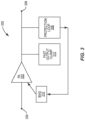
- the general concept is shown by a power amplifier system 300 in Figure 3 .
- the power amplifier system 300 may include a power amplifier stage 302 with an input node 304 and an output node 306.
- a feedback protection loop 308 may be coupled to the power amplifier stage 302 at the output node 306 or other location depending on the nature of the feedback protection loop.
- the feedback protection loop 308 may act to cause a bias circuit 310 to debias the power amplifier stage 302 when a proxy for the power level (e.g., a voltage level, a current level, a temperature, or an actual power level) exceeds a first threshold.
- An output clamp 312 may also be associated with or coupled to the output node 306.
- the output clamp 312 is comparatively fast relative to the feedback protection loop 308 but is activated when the power level at the output node 306 exceeds a second threshold.
- the power level at the output node 306 is higher at the second threshold than the power level at the output node 306 when the first threshold is reached even if the first threshold is not directly compared to the power level at the output node 306.
- the first threshold will be passed and the feedback protection loop 308 will begin to instruct the bias circuit 310 to debias the power amplifier stage 302.
- this feedback protection loop 308 is relatively slow, so the power consumed by the power amplifier stage 302 will continue to increase until it reaches the second threshold and the output clamp 312 begins to limit the power consumption.
- the second threshold is relatively high and because the output clamp 312 does not have to limit the power for an extended period of time, the size of the output clamp 312 may be relatively small (e.g., fewer stacked diodes).
- the feedback protection loop 308 will have had time to debias the power amplifier stage 302 sufficiently to prevent damage to the power amplifier stage 302 and the output clamp 312 may turn off.
- the thresholds may be programmable and their relationship can be adjusted through such programming. Specifically, switches may switch in/out diodes within a diode stack within the output clamp 312. Such switching may be controlled by a control circuit (not shown). The control circuit may further adjust a value within a register that is used by a comparator within the feedback protection loop 308. Other ways of programming the thresholds may also be used without departing from the present disclosure.
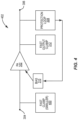
- Other elements remain identical, but the input clamp 400 may likewise be a small, fast clamp.
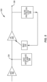
- FIG. 5 Another example aspect is a power amplifier system 500 shown in Figure 5 .
- a driver amplifier stage 502 is added before the input node 304 making the input clamp an interstage clamp 504, although functionally the interstage clamp 504 may be identical to the input clamp 400.
- Figure 6 illustrates a similar power amplifier system 600, which includes the driver amplifier stage 502 and the interstage clamp 504 as well as the output clamp 312.
- the clamps 312 and 504 may have different thresholds or the same threshold, and in either case, the threshold(s) are above the first threshold of the feedback protection loop 308.
- the feedback protection loop 308 may be an overcurrent protection loop, an overvoltage protection loop, an overpower protection loop, or an overtemperature protection loop. More details about such protection loops may be found in commonly owned U.S. Patent Application Serial No. 17/488,877, filed September 29, 2021 , which is hereby incorporated by reference in its entirety. Further, instead of a just a single feedback protection loop 308, there may be multiple feedback protection loops. For example, both an overcurrent and an overvoltage protection feedback protection loop may be present (or combined into a single loop).
- An example power amplifier system 700 illustrated in Figure 7 shows how myriad feedback protection loops and clamps may be used in harmony.
- the power amplifier system 700 may have a first power amplifier stage 702, which may be a driver amplifier stage and a second power amplifier stage 704, which may be an output amplifier stage.
- the first power amplifier stage 702 may be coupled to an input node 706 that receives an RF input signal (RFin) to be amplified.
- RFin RF input signal
- a DC blocking capacitor may be present between the input node 706 and the first power amplifier stage 702.
- An output of the first power amplifier stage 702 may be coupled to an input of the second power amplifier stage 704 with a node 708 therebetween.
- a DC blocking capacitor (not shown) may be present between the first power amplifier stage 702 and the second power amplifier stage 704.
- the output of the second power amplifier stage 704 may be coupled to a switching and filter circuit 710.
- the switching and filter circuit 710 may be coupled to an antenna 712.
- the switching and filter circuit 710 may include a distribution switch (DSW) 714, one or more filters 716 such as surface acoustic wave (SAW) filters, and an antenna switch 718.
- the switches 714, 718 may switch between frequency bands, cellular modes (e.g., 5G-NR versus 4G LTE), between transmit and receive modes, or the like and are not central to the present disclosure.
- the first power amplifier stage 702 may be biased by a first bias circuit 720.
- the second power amplifier stage 704 may be biased by a second bias circuit 722.
- the first power amplifier stage 702 may be protected by a first input clamp 724, which is relatively small and relatively fast.
- the first power amplifier stage 702 may further be protected by a power feedback protection loop 726 that detects an input power (Pin) with a Pin detector 728. If Pin is above a first threshold, a signal may be provided to the first bias circuit 720 to debias the first power amplifier stage 702. As described above, the first threshold may be lower than a second threshold at which the first input clamp 724 activates.
- the first power amplifier stage 702 may also be protected by a second feedback protection loop 730, which may, for example, be an overvoltage protection (OVP) loop.
- OVP overvoltage protection
- the second feedback protection loop 730 may send a signal to the first bias circuit 720 to debias the first power amplifier stage 702.
- the third threshold is likewise chosen to be lower than the second threshold of the first input clamp 724.
- the second power amplifier stage 704 may be protected by a clamp 732.
- the clamp 732 is an output clamp for the first power amplifier stage 702, it is an input or interstage clamp for the second power amplifier stage 704. As such the clamp 732 may protect both power amplifier stages 702 and 704.
- the threshold at which the clamp 732 turns on may be above the first and third thresholds.
- the second power amplifier stage 704 may also be protected by an output clamp 734.
- the second power amplifier stage 704 may also be protected by an overtemperature feedback protection loop 736, which provides an overtemperature condition signal to the second bias circuit 722 or to an overcurrent feedback protection loop (OCP) 738.
- OCP loop 738 may receive a current signal from a current detector 740.
- the OCP loop 738 may send a signal to the second bias circuit 722 to debias the second power amplifier stage 704.
- the second power amplifier stage 704 may also be protected by an overvoltage feedback protection loop (OVP) 742.
- OVP overvoltage feedback protection loop
- the thresholds at which the feedback protection loops 736, 738, 742 activate may be lower than the threshold of the clamps 732, 734.
- a power feedback protection loop 744 may measure reflected or reverse power (Prev) with a detector 746 and provide a signal to the bias circuit 722. Note that not all of the feedback protection loops 726, 730, 736, 738, 742 need be present. Likewise, additional feedback protection loops (e.g., an overtemperature feedback protection loop for the first power amplifier stage 702) may be present without departing from the scope of the present disclosure.
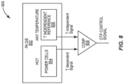
- FIG. 8 illustrates such an OTP loop 800 where a power amplifier die 802 has relatively hot power cells 804 (e.g., the power amplifier stages) and a temperature circuit 806.
- the power cells 804 provide a temperature dependent signal to a comparator 808.
- the temperature circuit 806 provides a temperature independent reference signal to the comparator 808. Based on a delta between the signals, the comparator 808 may generate an OTP control signal. Additional details are provided in Figure 9 , where the power cells 804 may include a temperature sensor 900 to provide the temperature dependent signal to the comparator 808.
- the temperature circuit 806 may include a bandgap reference circuit 902 and a scaling factor circuit 904.
- the temperature sensor 900 may be a proportional-to-absolute temperature (PTAT) sensor 1000 that is designed to provide decreasing voltage with increased device temperature (sometimes referred to as NTAT) or may be a PTAT sensor 1002 that is designed to provide an increasing voltage with increased device temperature.
- PTAT proportional-to-absolute temperature
- FIG. 11 Additional example details about a possible scaling factor circuit 904 are provided in Figure 11 , where a resistor divider circuit formed from resistors 1100 and 1102 are coupled to a current source 1104 and a transistor 1106 that forms the sensor 1002.
- the current source 1104 is controlled by the bandgap reference circuit 902 and an NTAT signal is provided by the transistor 1106.
- aspects of the present disclosure may be single ended (as illustrated above), differential, quadrature, or the like. Further, aspects of the present disclosure may be implemented through n-type material field effect transistors (FETs) (NFETs), p-type material FETs (PFETs), complementary metal oxide semiconductor (CMOS) FETs, bipolar junction transistors (BJTs), or the like. Further, aspects of the present disclosure may be made using gallium nitride (GaN), gallium arsenide (GaAs), silicon carbide (SiC) materials. Further, aspects of the present disclosure may be formed on silicon, silicon on insulator (SOI), silicon on sapphire (SOS), glass, or other substrates.
- FETs n-type material field effect transistors
- PFETs p-type material FETs
- CMOS complementary metal oxide semiconductor
- BJTs bipolar junction transistors
- aspects of the present disclosure may be made using gallium nitride (GaN), gallium arsen
- the power amplifier is initially protected by a fast-acting clamp circuit whose overall size is relatively limited. Subsequent operation allows a comparatively slowly acting feedback loop to dominate the protection of the power amplifier.
- the two protection circuits each optimized for a particular phase of protection, the overall size of associated protection circuitry may be diminished while still protecting the power amplifier from failure inducing conditions.
Landscapes
- Engineering & Computer Science (AREA)
- Power Engineering (AREA)
- Amplifiers (AREA)
Abstract
Description
- The present application claims priority to
U.S. Provisional Patent Application Serial No. 63/307,387 filed on February 7, 2022 - The technology of the disclosure relates generally to power amplifiers and particularly but not exclusively to power amplifiers with protection circuitry.
- Computing devices abound in modern society, and more particularly, mobile communication devices have become increasingly common. The prevalence of these mobile communication devices is driven in part by the many functions that are now enabled on such devices. Increased processing capabilities in such devices means that mobile communication devices have evolved from pure communication tools into sophisticated mobile entertainment centers, thus enabling enhanced user experiences. With the advent of the myriad functions available to such devices, there has been increased pressure to find ways to increase bandwidth for wireless communication that facilitates these functions. Accordingly, cellular wireless standards have evolved into the fifth-generation new radio (5G-NR) standards. These new cellular standards place additional burdens on power amplifiers used for the transmitters, requiring operation that consumes relatively large amounts of power and generates large amounts of waste heat. Protecting the power amplifiers creates an opportunity for innovation.
- Particular aspects are set out in the appended independent claims. Various optional embodiments are set out in the dependent claims.
- Aspects disclosed in the detailed description include a power amplifier with clamp and feedback protection circuitry. In an example aspect, the power amplifier is initially protected by a fast-acting clamp circuit whose overall size is relatively limited. Subsequent operation allows a comparatively slowly acting feedback loop to dominate the protection of the power amplifier. By providing the two protection circuits, each optimized for a particular phase of protection, the overall size of associated protection circuitry may be diminished while still protecting the power amplifier from failure inducing conditions.
- In this regard in one aspect, a power amplifier system is disclosed. The power amplifier system comprises a power amplifier stage comprising an input node and an output node. The power amplifier system also comprises a bias circuit coupled to the power amplifier stage and configured to provide a bias signal to the power amplifier stage. The power amplifier system also comprises a clamp coupled to the power amplifier stage, the clamp configured to limit a voltage level based on a first threshold. The power amplifier system also comprises a feedback protection loop coupled to the bias circuit and configured to detect an operating condition above a second threshold and send a signal to the bias circuit. The bias circuit is configured, responsive to the signal, to debias the power amplifier stage.
- In another aspect, a power amplifier system is disclosed. The power amplifier system comprises a power amplifier stage. The power amplifier system also comprises a bias circuit coupled to the power amplifier stage and configured to provide a bias signal to the power amplifier stage. The power amplifier system also comprises an overtemperature feedback protection loop coupled to the bias circuit and configured to cause the bias circuit to debias the power amplifier stage when a threshold temperature is reached. The overtemperature feedback protection loop comprises a temperature sensor physically proximate the power amplifier stage. The overtemperature feedback protection loop also comprises a temperature independent voltage source. The overtemperature feedback protection loop also comprises a comparator coupled to the temperature sensor and the temperature independent voltage source.
-
-
Figure 1 is a block diagram of a conventional power amplifier with a feedback protection circuit; -
Figure 2 is a block diagram of a conventional power amplifier with a clamp protection circuit; -
Figure 3 is a block diagram of a power amplifier having a feedback protection circuit and an output clamp protection circuit according to an example aspect of the present disclosure; -
Figure 4 is a block diagram of a power amplifier having a feedback protection circuit and two clamp protection circuits according to an example aspect of the present disclosure; -
Figure 5 is a block diagram of a power amplifier having a feedback protection circuit and an input clamp protection circuit according to an example aspect of the present disclosure; -
Figure 6 is a block diagram of a multi-stage power amplifier having a feedback protection circuit and two clamp protection circuits according to an example aspect of the present disclosure; -
Figure 7 is a block diagram of a multi-stage power amplifier having a plurality of feedback protection circuits and a plurality of clamp protection circuits according to an example aspect of the present disclosure; -
Figure 8 is a block diagram of an over-temperature protection circuit that may be used alone or in combination with the clamp circuit of the present disclosure; -
Figure 9 is a block diagram expanding on the reference circuit ofFigure 8 according to a first example aspect; -
Figure 10 is block diagram providing an alternate sensing circuit for the circuit ofFigure 8 ; and -
Figure 11 is a circuit diagram showing how a resistor divider may be used to scale the reference circuit ofFigure 8 . - The embodiments set forth below represent the necessary information to enable those skilled in the art to practice the embodiments and illustrate the best mode of practicing the embodiments. Upon reading the following description in light of the accompanying drawing figures, those skilled in the art will understand the concepts of the disclosure and will recognize applications of these concepts not particularly addressed herein. It should be understood that these concepts and applications fall within the scope of the disclosure and the accompanying claims.
- It will be understood that, although the terms first, second, etc. may be used herein to describe various elements, these elements should not be limited by these terms. These terms are only used to distinguish one element from another. For example, a first element could be termed a second element, and, similarly, a second element could be termed a first element, without departing from the scope of the present disclosure. As used herein, the term "and/or" includes any and all combinations of one or more of the associated listed items.
- It will be understood that when an element such as a layer, region, or substrate is referred to as being "on" or extending "onto" another element, it can be directly on or extend directly onto the other element or intervening elements may also be present. In contrast, when an element is referred to as being "directly on" or extending "directly onto" another element, there are no intervening elements present. Likewise, it will be understood that when an element such as a layer, region, or substrate is referred to as being "over" or extending "over" another element, it can be directly over or extend directly over the other element or intervening elements may also be present. In contrast, when an element is referred to as being "directly over" or extending "directly over" another element, there are no intervening elements present. It will also be understood that when an element is referred to as being "connected" or "coupled" to another element, it can be directly connected or coupled to the other element or intervening elements may be present. In contrast, when an element is referred to as being "directly connected" or "directly coupled" to another element, there are no intervening elements present.
- Relative terms such as "below" or "above" or "upper" or "lower" or "horizontal" or "vertical" may be used herein to describe a relationship of one element, layer, or region to another element, layer, or region as illustrated in the Figures. It will be understood that these terms and those discussed above are intended to encompass different orientations of the device in addition to the orientation depicted in the Figures.
- The terminology used herein is for the purpose of describing particular embodiments only and is not intended to be limiting of the disclosure. As used herein, the singular forms "a," "an," and "the" are intended to include the plural forms as well, unless the context clearly indicates otherwise. It will be further understood that the terms "comprises," "comprising," "includes," and/or "including" when used herein specify the presence of stated features, integers, steps, operations, elements, and/or components, but do not preclude the presence or addition of one or more other features, integers, steps, operations, elements, components, and/or groups thereof.
- Unless otherwise defined, all terms (including technical and scientific terms) used herein have the same meaning as commonly understood by one of ordinary skill in the art to which this disclosure belongs. It will be further understood that terms used herein should be interpreted as having a meaning that is consistent with their meaning in the context of this specification and the relevant art and will not be interpreted in an idealized or overly formal sense unless expressly so defined herein.
- Aspects disclosed in the detailed description include a power amplifier with clamp and feedback protection circuitry. In an example aspect, the power amplifier is initially protected by a fast-acting clamp circuit whose overall size is relatively limited. Subsequent operation allows a comparatively slowly acting feedback loop to dominate the protection of the power amplifier. By providing the two protection circuits, each optimized for a particular phase of protection, the overall size of associated protection circuitry may be diminished while still protecting the power amplifier from failure inducing conditions.
- Before addressing example aspects of the present disclosure, a brief overview of traditional ways to protect a power amplifier are discussed with reference to
Figures 1 and2 . A discussion of example aspects of the present disclosure begins below with reference toFigure 3 . - In this regard,
Figure 1 is a block diagram of apower amplifier system 100 that includes apower amplifier stage 102 having aninput node 104 configured to receive a radio frequency (RF) alternating current (AC) signal and anoutput node 106 configured to provide an amplified signal. Acapacitor 108 blocks direct current (DC) signals at theinput node 104 from reaching aninput 112 of thepower amplifier stage 102. Abias circuit 110 may be coupled to theinput 112 of thepower amplifier stage 102 through aballast resistor 114. Thepower amplifier stage 102 may further be coupled to asupply voltage 116 and aground 118. - The
power amplifier stage 102 may be protected from runaway power conditions through a firstfeedback protection loop 120, which may include acurrent detector 122 that provides a signal to thebias circuit 110. When thecurrent detector 122 detects a current at thebias circuit 110 above a predetermined threshold, the firstfeedback protection loop 120 may cause thebias circuit 110 to debias thepower amplifier stage 102, thereby reducing the power used by thepower amplifier stage 102. - Similarly, the
power amplifier stage 102 may be protected from runaway power conditions through a secondfeedback protection loop 124, which may include avoltage detector 126 that provides a signal to thebias circuit 110. When thevoltage detector 126 detects a voltage at thesupply voltage 116 above a predetermined threshold, the secondfeedback protection loop 124 may cause thebias circuit 110 to debias thepower amplifier stage 102, thereby reducing the power used by thepower amplifier stage 102. Note that in some instances, the secondfeedback protection loop 124 may be combined with the first feedback protection loop 120 (denoted by arrow 128). The end result of such combination is still a signal being provided to thebias circuit 110 to debias thepower amplifier stage 102. - Traditionally, the
feedback protection loops detectors bias circuit 110. Thebias circuit 110 in turn adjusts a voltage level or current level at theinput 112 to lower the signal being amplified by thepower amplifier stage 102. This adjustment takes time during which thepower amplifier stage 102 may still generate sufficient heat to damage thepower amplifier stage 102. - Instead of using the
feedback protection loops power amplifier system 200 inFigure 2 . In particular, thepower amplifier system 200 may include apower amplifier stage 202 with aninput node 204 and anoutput node 206. Anoutput clamp 208 may be coupled to theoutput node 206. Traditionally, theoutput clamp 208 is formed from a plurality of stacked diodes 210(1)-210(N). Additionally, thepower amplifier system 200 may include aninput clamp 212 coupled to theinput node 204. Note that where thepower amplifier stage 202 is part of a chain of power amplifier stages (not shown), theinput clamp 212 may be referred to as an interstage clamp and may also be coupled to an output of a prior power amplifier stage. Theinput clamp 212 may be formed from a plurality ofdiodes 214 andtransistors 216. When sufficient diodes 210(1)-210(N) are gathered, the total space required to instantiate such diodes is relatively large, being, in many instances, equal in size to thepower amplifier stage 202. However, the large size allows theclamps power amplifier stage 202 and protecting thepower amplifier stage 202 from harm. The downside of this fast acting protection is the aforementioned size and power consumption of the diodes. - Neither solution alone provides a perfect solution for the need to protect the power amplifier stage. Example aspects of the present disclosure take the best of both solutions and combine them into a whole that exceeds the sum of its parts. Specifically, a relatively small, but fast acting output clamp may be used in conjunction with a relatively slow feedback protection loop. In particular, the feedback protection loop may activate at a first threshold, but the latency of the feedback protection loop means that the output power for the power amplifier stage will likely continue to rise, passing a second threshold associated with the clamp, where the second threshold is greater than the first threshold. When this second threshold is reached, the clamp quickly acts to limit the power to the second threshold. Since the second threshold is greater than the first threshold, the feedback protection loop continues to debias the power amplifier stage through the bias circuit, eventually bringing the power down to the first threshold such that the clamp is no longer active.
- The general concept is shown by a
power amplifier system 300 inFigure 3 . Thepower amplifier system 300 may include apower amplifier stage 302 with aninput node 304 and anoutput node 306. Afeedback protection loop 308 may be coupled to thepower amplifier stage 302 at theoutput node 306 or other location depending on the nature of the feedback protection loop. Thefeedback protection loop 308 may act to cause abias circuit 310 to debias thepower amplifier stage 302 when a proxy for the power level (e.g., a voltage level, a current level, a temperature, or an actual power level) exceeds a first threshold. Anoutput clamp 312 may also be associated with or coupled to theoutput node 306. Theoutput clamp 312 is comparatively fast relative to thefeedback protection loop 308 but is activated when the power level at theoutput node 306 exceeds a second threshold. The power level at theoutput node 306 is higher at the second threshold than the power level at theoutput node 306 when the first threshold is reached even if the first threshold is not directly compared to the power level at theoutput node 306. - Thus, in operation, as the power consumed by the
power amplifier stage 302 increases (as measured by a proxy or an actual power level), the first threshold will be passed and thefeedback protection loop 308 will begin to instruct thebias circuit 310 to debias thepower amplifier stage 302. However, thisfeedback protection loop 308 is relatively slow, so the power consumed by thepower amplifier stage 302 will continue to increase until it reaches the second threshold and theoutput clamp 312 begins to limit the power consumption. Because the second threshold is relatively high and because theoutput clamp 312 does not have to limit the power for an extended period of time, the size of theoutput clamp 312 may be relatively small (e.g., fewer stacked diodes). Before theoutput clamp 312 fails, thefeedback protection loop 308 will have had time to debias thepower amplifier stage 302 sufficiently to prevent damage to thepower amplifier stage 302 and theoutput clamp 312 may turn off. Note that the thresholds may be programmable and their relationship can be adjusted through such programming. Specifically, switches may switch in/out diodes within a diode stack within theoutput clamp 312. Such switching may be controlled by a control circuit (not shown). The control circuit may further adjust a value within a register that is used by a comparator within thefeedback protection loop 308. Other ways of programming the thresholds may also be used without departing from the present disclosure. - There are many variations of this hybrid protection scheme. For example, as shown in
Figure 4 , aninput clamp 400 to form apower amplifier system 402. Other elements remain identical, but theinput clamp 400 may likewise be a small, fast clamp. - Another example aspect is a power amplifier system 500 shown in
Figure 5 . In particular, adriver amplifier stage 502 is added before theinput node 304 making the input clamp aninterstage clamp 504, although functionally theinterstage clamp 504 may be identical to theinput clamp 400. -
Figure 6 illustrates a similarpower amplifier system 600, which includes thedriver amplifier stage 502 and theinterstage clamp 504 as well as theoutput clamp 312. Theclamps feedback protection loop 308. - While the above discussion illustrates only a single generic
feedback protection loop 308, it should be appreciated that thefeedback protection loop 308 may be an overcurrent protection loop, an overvoltage protection loop, an overpower protection loop, or an overtemperature protection loop. More details about such protection loops may be found in commonly ownedU.S. Patent Application Serial No. 17/488,877, filed September 29, 2021 feedback protection loop 308, there may be multiple feedback protection loops. For example, both an overcurrent and an overvoltage protection feedback protection loop may be present (or combined into a single loop). - An example power amplifier system 700, illustrated in
Figure 7 shows how myriad feedback protection loops and clamps may be used in harmony. In particular, the power amplifier system 700 may have a firstpower amplifier stage 702, which may be a driver amplifier stage and a secondpower amplifier stage 704, which may be an output amplifier stage. The firstpower amplifier stage 702 may be coupled to aninput node 706 that receives an RF input signal (RFin) to be amplified. While not shown, a DC blocking capacitor may be present between theinput node 706 and the firstpower amplifier stage 702. An output of the firstpower amplifier stage 702 may be coupled to an input of the secondpower amplifier stage 704 with anode 708 therebetween. Again, a DC blocking capacitor (not shown) may be present between the firstpower amplifier stage 702 and the secondpower amplifier stage 704. The output of the secondpower amplifier stage 704 may be coupled to a switching andfilter circuit 710. The switching andfilter circuit 710 may be coupled to anantenna 712. Further, the switching andfilter circuit 710 may include a distribution switch (DSW) 714, one ormore filters 716 such as surface acoustic wave (SAW) filters, and anantenna switch 718. Theswitches power amplifier stage 702 may be biased by afirst bias circuit 720. The secondpower amplifier stage 704 may be biased by asecond bias circuit 722. - The first
power amplifier stage 702 may be protected by afirst input clamp 724, which is relatively small and relatively fast. The firstpower amplifier stage 702 may further be protected by a powerfeedback protection loop 726 that detects an input power (Pin) with aPin detector 728. If Pin is above a first threshold, a signal may be provided to thefirst bias circuit 720 to debias the firstpower amplifier stage 702. As described above, the first threshold may be lower than a second threshold at which thefirst input clamp 724 activates. The firstpower amplifier stage 702 may also be protected by a secondfeedback protection loop 730, which may, for example, be an overvoltage protection (OVP) loop. When the secondfeedback protection loop 730 detects voltage above a third threshold as a proxy for a power level, the secondfeedback protection loop 730 may send a signal to thefirst bias circuit 720 to debias the firstpower amplifier stage 702. The third threshold is likewise chosen to be lower than the second threshold of thefirst input clamp 724. - The second
power amplifier stage 704 may be protected by a clamp 732. Note that while the clamp 732 is an output clamp for the firstpower amplifier stage 702, it is an input or interstage clamp for the secondpower amplifier stage 704. As such the clamp 732 may protect both power amplifier stages 702 and 704. Note that the threshold at which the clamp 732 turns on may be above the first and third thresholds. The secondpower amplifier stage 704 may also be protected by anoutput clamp 734. The secondpower amplifier stage 704 may also be protected by an overtemperaturefeedback protection loop 736, which provides an overtemperature condition signal to thesecond bias circuit 722 or to an overcurrent feedback protection loop (OCP) 738. TheOCP loop 738 may receive a current signal from acurrent detector 740. Based on the current signal and/or the overtemperature condition signal, theOCP loop 738 may send a signal to thesecond bias circuit 722 to debias the secondpower amplifier stage 704. The secondpower amplifier stage 704 may also be protected by an overvoltage feedback protection loop (OVP) 742. Again, the thresholds at which thefeedback protection loops clamps 732, 734. - Additionally, a power
feedback protection loop 744 may measure reflected or reverse power (Prev) with adetector 746 and provide a signal to thebias circuit 722. Note that not all of thefeedback protection loops - While the previously incorporated '877 application provides many possible feedback protection loop details, the present disclosure also provides an example overtemperature protection (OTP) loop as described with reference to
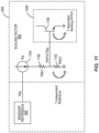
Figures 8-11 .Figure 8 illustrates such anOTP loop 800 where a power amplifier die 802 has relatively hot power cells 804 (e.g., the power amplifier stages) and atemperature circuit 806. Thepower cells 804 provide a temperature dependent signal to acomparator 808. Thetemperature circuit 806 provides a temperature independent reference signal to thecomparator 808. Based on a delta between the signals, thecomparator 808 may generate an OTP control signal. Additional details are provided inFigure 9 , where thepower cells 804 may include atemperature sensor 900 to provide the temperature dependent signal to thecomparator 808. Thetemperature circuit 806 may include abandgap reference circuit 902 and ascaling factor circuit 904. - As illustrated in
Figure 10 , thetemperature sensor 900 may be a proportional-to-absolute temperature (PTAT)sensor 1000 that is designed to provide decreasing voltage with increased device temperature (sometimes referred to as NTAT) or may be aPTAT sensor 1002 that is designed to provide an increasing voltage with increased device temperature. - Additional example details about a possible
scaling factor circuit 904 are provided inFigure 11 , where a resistor divider circuit formed fromresistors current source 1104 and atransistor 1106 that forms thesensor 1002. Thecurrent source 1104 is controlled by thebandgap reference circuit 902 and an NTAT signal is provided by thetransistor 1106. - As a further note, aspects of the present disclosure may be single ended (as illustrated above), differential, quadrature, or the like. Further, aspects of the present disclosure may be implemented through n-type material field effect transistors (FETs) (NFETs), p-type material FETs (PFETs), complementary metal oxide semiconductor (CMOS) FETs, bipolar junction transistors (BJTs), or the like. Further, aspects of the present disclosure may be made using gallium nitride (GaN), gallium arsenide (GaAs), silicon carbide (SiC) materials. Further, aspects of the present disclosure may be formed on silicon, silicon on insulator (SOI), silicon on sapphire (SOS), glass, or other substrates.
- Therefore, from one perspective, there have been described approaches for a power amplifier with clamp and feedback protection circuitry. In one aspect, the power amplifier is initially protected by a fast-acting clamp circuit whose overall size is relatively limited. Subsequent operation allows a comparatively slowly acting feedback loop to dominate the protection of the power amplifier. By providing the two protection circuits, each optimized for a particular phase of protection, the overall size of associated protection circuitry may be diminished while still protecting the power amplifier from failure inducing conditions.
- Further examples are set out in the following numbered clauses:
-
Clause 1. A power amplifier system comprising: a power amplifier stage comprising an input node and an output node; a bias circuit coupled to the power amplifier stage and configured to provide a bias signal to the power amplifier stage; a clamp coupled to the power amplifier stage, the clamp configured to limit a voltage level based on a first threshold; and a feedback protection loop coupled to the bias circuit and configured to detect an operating condition above a second threshold and send a signal to the bias circuit, wherein the bias circuit is configured, responsive to the signal, to debias the power amplifier stage. -
Clause 2. The power amplifier system ofclause 1, wherein the clamp is coupled to the input node. - Clause 3. The power amplifier system of
clause - Clause 4. The power amplifier system of
clause - Clause 5. The power amplifier system of any preceding clause, wherein the first threshold and the second threshold are proxies for overpower conditions and the second threshold is lower than the first threshold.
- Clause 6. The power amplifier system of any preceding clause, wherein the feedback protection loop is configured to adjust power within the power amplifier stage slower than the clamp adjusts power within the power amplifier stage.
- Clause 7. The power amplifier system of clause 6, wherein the clamp is configured to turn off when the feedback protection loop begins reducing power within the power amplifier stage.
- Clause 8. The power amplifier system of any preceding clause, wherein the feedback protection loop comprises an overvoltage feedback protection loop.
- Clause 9. The power amplifier system of any preceding clause, wherein the feedback protection loop comprises an overcurrent feedback protection loop.
- Clause 10. The power amplifier system of any preceding clause, wherein the feedback protection loop comprises an overtemperature feedback protection loop.
- Clause 11. The power amplifier system of any preceding clause, wherein the feedback protection loop comprises an overpower feedback protection loop.
- Clause 12. The power amplifier system of any preceding clause, further comprising a second power amplifier stage coupled to the input node.
- Clause 13. The power amplifier system of any preceding clause, further comprising a second clamp coupled to the output node and wherein the clamp is coupled to the input node.
- Clause 14. The power amplifier system of any preceding clause, wherein the feedback protection loop comprises a plurality of feedback protection loops selected from the group consisting of: an overcurrent feedback protection loop, an overvoltage feedback protection loop, an overtemperature feedback protection loop, and an overpower feedback protection loop.
- Clause 15. The power amplifier system of any preceding, wherein the first threshold and the second threshold are configured to be programmed dynamically.
- Clause 16. A power amplifier system comprising: a power amplifier stage; a bias circuit coupled to the power amplifier stage and configured to provide a bias signal to the power amplifier stage; and an overtemperature feedback protection loop coupled to the bias circuit and configured to cause the bias circuit to debias the power amplifier stage when a threshold temperature is reached, the overtemperature feedback protection loop comprising: a temperature sensor physically proximate the power amplifier stage; a temperature independent voltage source; and a comparator coupled to the temperature sensor and the temperature independent voltage source.
- Clause 17. The power amplifier system of clause 16, further comprising a second feedback protection loop coupled to the bias circuit.
- Clause 18. The power amplifier system of clause 17, wherein the comparator is coupled to the second feedback protection loop.
- It is also noted that the operational steps described in any of the example aspects herein are described to provide examples and discussion. The operations described may be performed in numerous different sequences other than the illustrated sequences. Furthermore, operations described in a single operational step may actually be performed in a number of different steps. Additionally, one or more operational steps discussed in the example aspects may be combined. It is to be understood that the operational steps illustrated in the flowchart diagrams may be subject to numerous different modifications as will be readily apparent to one of skill in the art. Those of skill in the art will also understand that information and signals may be represented using any of a variety of different technologies and techniques. For example, data, instructions, commands, information, signals, bits, symbols, and chips that may be referenced throughout the above description may be represented by voltages, currents, electromagnetic waves, magnetic fields or particles, optical fields or particles, or any combination thereof.
- The previous description of the disclosure is provided to enable any person skilled in the art to make or use the disclosure. Various modifications to the disclosure will be readily apparent to those skilled in the art, and the generic principles defined herein may be applied to other variations. Thus, the disclosure is not intended to be limited to the examples and designs described herein but is to be accorded the widest scope consistent with the principles and novel features disclosed herein.
Claims (14)
- A power amplifier system comprising:a power amplifier stage comprising an input node and an output node;a bias circuit coupled to the power amplifier stage and configured to provide a bias signal to the power amplifier stage;a clamp coupled to the power amplifier stage, the clamp configured to limit a voltage level based on a first threshold; anda feedback protection loop coupled to the bias circuit and configured to detect an operating condition above a second threshold and send a signal to the bias circuit, wherein the bias circuit is configured, responsive to the signal, to debias the power amplifier stage.
- The power amplifier system of claim 1, wherein the clamp is coupled to the input node.
- The power amplifier system of claim 1 or 2, wherein the clamp is coupled to the output node.
- The power amplifier system of claim 1, 2 or 3, wherein the clamp comprises a plurality of stacked diodes.
- The power amplifier system of any preceding claim, wherein the first threshold and the second threshold are proxies for overpower conditions and the second threshold is lower than the first threshold.
- The power amplifier system of any preceding claim, wherein the feedback protection loop is configured to adjust power within the power amplifier stage slower than the clamp adjusts power within the power amplifier stage.
- The power amplifier system of claim 6, wherein the clamp is configured to turn off when the feedback protection loop begins reducing power within the power amplifier stage.
- The power amplifier system of any preceding claim, further comprising a second power amplifier stage coupled to the input node.
- The power amplifier system of any preceding claim, further comprising a second clamp coupled to the output node and wherein the clamp is coupled to the input node.
- The power amplifier system of any preceding claim, wherein the feedback protection loop comprises a one or more feedback protection loops selected from the group consisting of: an overcurrent feedback protection loop, an overvoltage feedback protection loop, an overtemperature feedback protection loop, and an overpower feedback protection loop.
- The power amplifier system of any preceding claim, wherein the first threshold and the second threshold are configured to be programmed dynamically.
- A power amplifier system comprising:a power amplifier stage;a bias circuit coupled to the power amplifier stage and configured to provide a bias signal to the power amplifier stage; andan overtemperature feedback protection loop coupled to the bias circuit and configured to cause the bias circuit to debias the power amplifier stage when a threshold temperature is reached, the overtemperature feedback protection loop comprising:a temperature sensor physically proximate the power amplifier stage;a temperature independent voltage source; anda comparator coupled to the temperature sensor and the temperature independent voltage source.
- The power amplifier system of claim 12, further comprising a second feedback protection loop coupled to the bias circuit.
- The power amplifier system of claim 13, wherein the comparator is coupled to the second feedback protection loop.
Applications Claiming Priority (2)
| Application Number | Priority Date | Filing Date | Title |
|---|---|---|---|
| US202263307387P | 2022-02-07 | 2022-02-07 | |
| US17/805,316 US12580526B2 (en) | 2022-02-07 | 2022-06-03 | Power amplifier with clamp and feedback protection circuitry |
Publications (1)
| Publication Number | Publication Date |
|---|---|
| EP4224709A1 true EP4224709A1 (en) | 2023-08-09 |
Family
ID=85198904
Family Applications (1)
| Application Number | Title | Priority Date | Filing Date |
|---|---|---|---|
| EP23155394.2A Pending EP4224709A1 (en) | 2022-02-07 | 2023-02-07 | Power amplifier with clamp and protection feedback circuitry |
Country Status (2)
| Country | Link |
|---|---|
| US (2) | US12580526B2 (en) |
| EP (1) | EP4224709A1 (en) |
Cited By (2)
| Publication number | Priority date | Publication date | Assignee | Title |
|---|---|---|---|---|
| WO2026043593A1 (en) * | 2024-08-23 | 2026-02-26 | Qualcomm Incorporated | Voltage and current protection for an amplifier |
| WO2026043649A1 (en) * | 2024-08-22 | 2026-02-26 | Qorvo Us, Inc. | Power amplifier circuitry with temperature based biasing |
Citations (2)
| Publication number | Priority date | Publication date | Assignee | Title |
|---|---|---|---|---|
| US20020125945A1 (en) * | 2001-03-08 | 2002-09-12 | Taylor Stewart Sidney | Method and apparatus for protecting radio frequency power amplifiers |
| US20040239428A1 (en) * | 2002-08-09 | 2004-12-02 | Triquint Semiconductor, Inc. | Active protection circuit for load mismatched power amplifier |
Family Cites Families (56)
| Publication number | Priority date | Publication date | Assignee | Title |
|---|---|---|---|---|
| US3641451A (en) | 1970-02-24 | 1972-02-08 | Motorola Inc | Amplifier protection circuit |
| US4122400A (en) | 1976-11-08 | 1978-10-24 | Rca Corporation | Amplifier protection circuit |
| US4893158A (en) | 1987-06-22 | 1990-01-09 | Nissan Motor Co., Ltd. | MOSFET device |
| JPH06103806B2 (en) | 1990-07-19 | 1994-12-14 | 株式会社エヌエフ回路設計ブロック | Power amplifier protection circuit |
| US5357089A (en) | 1993-02-26 | 1994-10-18 | Harris Corporation | Circuit and method for extending the safe operating area of a BJT |
| WO1995031035A1 (en) | 1994-05-10 | 1995-11-16 | Ericsson Inc. | Thermally controlled, linear power reduction circuit |
| JP3127813B2 (en) | 1995-12-05 | 2001-01-29 | ヤマハ株式会社 | Audio amplifier protection circuit |
| US6469919B1 (en) | 1999-07-22 | 2002-10-22 | Eni Technology, Inc. | Power supplies having protection circuits |
| AU2003260845A1 (en) | 2002-10-03 | 2004-04-23 | Koninklijke Philips Electronics N.V. | Power amplifier and method for power amplification |
| US7268990B1 (en) | 2003-05-15 | 2007-09-11 | Marvell International Ltd. | Power amplifier protection |
| US7193459B1 (en) | 2004-06-23 | 2007-03-20 | Rf Micro Devices, Inc. | Power amplifier control technique for enhanced efficiency |
| WO2006033052A1 (en) | 2004-09-21 | 2006-03-30 | Koninklijke Philips Electronics N.V. | Peak voltage protection circuit and method |
| US7729672B2 (en) | 2006-03-22 | 2010-06-01 | Qualcomm, Incorporated | Dynamic bias control in power amplifier |
| US7733176B2 (en) | 2006-09-08 | 2010-06-08 | Infineon Technologies Ag | System and method for power amplifier output power control |
| JP4685836B2 (en) | 2007-05-28 | 2011-05-18 | パナソニック株式会社 | High frequency power amplifier |
| US8586256B2 (en) | 2007-07-10 | 2013-11-19 | Seiko Instruments Inc. | Power supply apparatus |
| US7852063B2 (en) | 2008-06-04 | 2010-12-14 | Silicon Storage Technology, Inc. | Integrated power detector with temperature compensation for fully-closed loop control |
| EP2401812B1 (en) | 2009-02-25 | 2013-11-13 | Nxp B.V. | Method and apparatus for maintaining circuit stability |
| US8385854B2 (en) | 2009-05-21 | 2013-02-26 | Qualcomm Incorporated | Adaptive parametric power amplifier protection circuit |
| US8274336B1 (en) | 2009-09-29 | 2012-09-25 | Amalfi Semiconductor, Inc. | Saturated power amplifier system |
| JP2011176592A (en) | 2010-02-24 | 2011-09-08 | Tdk Corp | Temperature compensation circuit and power amplifier |
| US8487705B2 (en) | 2010-05-26 | 2013-07-16 | Triquint Semiconductor, Inc. | Protection circuit for radio frequency power amplifier |
| WO2013099077A1 (en) | 2011-12-28 | 2013-07-04 | パナソニック株式会社 | Power amplifying apparatus, rf module and resistor |
| US10027287B1 (en) | 2013-02-20 | 2018-07-17 | Micro Mobio Corporation | World band frequency front end module, system and method thereof |
| CN104641553B (en) * | 2013-07-05 | 2017-07-11 | 株式会社村田制作所 | Power amplifier module |
| EP3020129B1 (en) | 2013-07-09 | 2021-12-08 | Skyworks Solutions, Inc. | Power amplifier with input power protection circuits |
| US9553549B2 (en) | 2014-05-28 | 2017-01-24 | Avago Technologies General Ip (Singapore) Pte. Ltd. | Hybrid power amplifier having electrical and thermal conduction path |
| US9705452B2 (en) | 2015-10-30 | 2017-07-11 | Avago Technologies General Ip (Singapore) Pte. Ltd. | Protection circuit for power amplifier |
| CN106169915B (en) | 2016-06-30 | 2020-07-31 | 唯捷创芯(天津)电子技术股份有限公司 | Multi-gain mode power amplifier, chip and communication terminal |
| TWI629844B (en) * | 2016-10-28 | 2018-07-11 | 偉詮電子股份有限公司 | System for dynamically controlling over voltage protection and voltage converter |
| US10291191B2 (en) | 2016-11-04 | 2019-05-14 | Qorvo Us, Inc. | Low leakage protection circuit for RF power amplifier |
| JP6825412B2 (en) | 2017-02-21 | 2021-02-03 | オムロン株式会社 | Motor control device |
| US11227862B2 (en) * | 2017-02-28 | 2022-01-18 | Murata Manufacturing Co., Ltd. | Semiconductor device |
| US10666200B2 (en) | 2017-04-04 | 2020-05-26 | Skyworks Solutions, Inc. | Apparatus and methods for bias switching of power amplifiers |
| CN107395144B (en) | 2017-07-05 | 2020-01-10 | 唯捷创芯(天津)电子技术股份有限公司 | Radio frequency power amplifier, chip and communication terminal based on power detection feedback |
| US10840856B2 (en) | 2017-07-25 | 2020-11-17 | Skyworks Solutions, Inc. | Apparatus and method for surge protection of a charge-pump powered power amplifier |
| TWI649961B (en) | 2017-08-22 | 2019-02-01 | 立積電子股份有限公司 | Power amplifier and protection circuit for use in rf active circuit |
| JP7149104B2 (en) | 2018-05-28 | 2022-10-06 | ローム株式会社 | Semiconductor integrated circuits, audio output devices, electronic equipment |
| US11277211B2 (en) * | 2018-09-24 | 2022-03-15 | Andrew Wireless Systems Gmbh | Methods and apparatuses for power control |
| US11476806B2 (en) | 2019-10-03 | 2022-10-18 | Skyworks Solutions, Inc. | Jump-start power amplifier boost converter |
| KR102891995B1 (en) | 2019-10-30 | 2025-11-28 | 삼성전자주식회사 | Protection circuit in a electronic device and therfor method |
| CN112803901B (en) | 2019-11-13 | 2025-03-14 | 武汉杰开科技有限公司 | A power amplifier based on adaptive overcurrent protection |
| US11677365B2 (en) | 2020-01-08 | 2023-06-13 | Qorvo Us, Inc. | Envelope tracking power management apparatus incorporating multiple power amplifiers |
| KR102778143B1 (en) | 2020-01-20 | 2025-03-06 | 삼성전기주식회사 | Power amplifier and power amplifier module |
| FR3107410B1 (en) | 2020-02-17 | 2022-05-06 | St Microelectronics Int Nv | RADIO FREQUENCY POWER AMPLIFIER |
| US11545945B2 (en) | 2020-03-04 | 2023-01-03 | Qorvo Us, Inc. | Apparatus and method for calibrating an envelope tracking lookup table |
| CN111740710B (en) | 2020-06-03 | 2025-04-01 | 唯捷创芯(天津)电子技术股份有限公司 | RF power amplifier, RF front-end module and communication terminal |
| GB2608004B (en) | 2020-06-19 | 2024-09-04 | Cirrus Logic Int Semiconductor Ltd | Protection circuitry |
| JP7547987B2 (en) * | 2020-12-18 | 2024-09-10 | 株式会社村田製作所 | Power Amplifiers |
| US11799327B2 (en) | 2021-02-24 | 2023-10-24 | Epirus, Inc. | Systems and methods for wireless power delivery |
| US12155353B2 (en) | 2021-09-29 | 2024-11-26 | Qorvo Us, Inc. | Power amplifier with protection loops |
| US12273076B2 (en) | 2021-09-29 | 2025-04-08 | Qorvo Us, Inc. | Power amplifier with protection loop |
| CN113746440B (en) * | 2021-11-05 | 2022-02-25 | 广州慧智微电子股份有限公司 | Power amplifier protection circuit and method for preventing final-stage input power from being overlarge |
| CN114070212A (en) | 2022-01-18 | 2022-02-18 | 唯捷创芯(天津)电子技术股份有限公司 | Radio frequency front-end module with current protection function and corresponding electronic equipment |
| EP4483488A1 (en) | 2022-02-23 | 2025-01-01 | Qorvo US, Inc. | Power amplifier with protection loop |
| US20230387867A1 (en) | 2022-05-26 | 2023-11-30 | Qorvo Us, Inc. | Power protection loop for amplifier chain elements |
-
2022
- 2022-06-03 US US17/805,316 patent/US12580526B2/en active Active
-
2023
- 2023-02-07 EP EP23155394.2A patent/EP4224709A1/en active Pending
-
2025
- 2025-07-24 US US19/279,204 patent/US20250350248A1/en active Pending
Patent Citations (2)
| Publication number | Priority date | Publication date | Assignee | Title |
|---|---|---|---|---|
| US20020125945A1 (en) * | 2001-03-08 | 2002-09-12 | Taylor Stewart Sidney | Method and apparatus for protecting radio frequency power amplifiers |
| US20040239428A1 (en) * | 2002-08-09 | 2004-12-02 | Triquint Semiconductor, Inc. | Active protection circuit for load mismatched power amplifier |
Non-Patent Citations (1)
| Title |
|---|
| ANDRE VAN BEZOOIJEN ET AL: "Over-Temperature Protection by Adaptive Output Power Control", THE 9TH EUROPEAN CONFERENCE ON WIRELESS TECHNOLOGY, IEEE, PISCATAWAY, NJ, US, 10 September 2006 (2006-09-10), pages 350 - 352, XP031005314, ISBN: 978-2-9600551-5-3 * |
Cited By (2)
| Publication number | Priority date | Publication date | Assignee | Title |
|---|---|---|---|---|
| WO2026043649A1 (en) * | 2024-08-22 | 2026-02-26 | Qorvo Us, Inc. | Power amplifier circuitry with temperature based biasing |
| WO2026043593A1 (en) * | 2024-08-23 | 2026-02-26 | Qualcomm Incorporated | Voltage and current protection for an amplifier |
Also Published As
| Publication number | Publication date |
|---|---|
| US20250350248A1 (en) | 2025-11-13 |
| US12580526B2 (en) | 2026-03-17 |
| US20230253930A1 (en) | 2023-08-10 |
Similar Documents
| Publication | Publication Date | Title |
|---|---|---|
| US20250350248A1 (en) | Power amplifier with clamp and feedback protection circuitry | |
| US10418945B2 (en) | Dynamic error vector magnitude compensation | |
| TWI713304B (en) | Apparatus and methods for programmable low dropout regulators for radio frequency electronics | |
| TW202241063A (en) | Variable current drive for isolated gate drivers | |
| US12034410B2 (en) | Overvoltage protection for power amplifier with soft shutdown | |
| US10291191B2 (en) | Low leakage protection circuit for RF power amplifier | |
| JP2002076791A (en) | Power amplifier module | |
| US7710204B2 (en) | Adaptive protection circuit for a power amplifier | |
| US11152897B2 (en) | Power amplifier and power amplifier module | |
| KR20240076818A (en) | Power amplifier with protection loop | |
| KR20240145003A (en) | Power amplifier with protection loop | |
| KR20240076817A (en) | Power amplifier with protection loop | |
| EP1391046B1 (en) | Non-linear transistor circuits with thermal stability | |
| CN116566335A (en) | Power amplifier with clamping and feedback protection circuitry | |
| HK40090819A (en) | Power amplifier with clamp and feedback protection circuitry | |
| KR20230165123A (en) | power protection loop for amplifier chain elements | |
| HK40096525A (en) | Power protection loop for amplifier chain elements | |
| CN117134718A (en) | Power Protection Loops for Amplifier Chain Components | |
| HK40105231A (en) | Power amplifier with protection loop |
Legal Events
| Date | Code | Title | Description |
|---|---|---|---|
| PUAI | Public reference made under article 153(3) epc to a published international application that has entered the european phase |
Free format text: ORIGINAL CODE: 0009012 |
|
| STAA | Information on the status of an ep patent application or granted ep patent |
Free format text: STATUS: THE APPLICATION HAS BEEN PUBLISHED |
|
| AK | Designated contracting states |
Kind code of ref document: A1 Designated state(s): AL AT BE BG CH CY CZ DE DK EE ES FI FR GB GR HR HU IE IS IT LI LT LU LV MC ME MK MT NL NO PL PT RO RS SE SI SK SM TR |
|
| STAA | Information on the status of an ep patent application or granted ep patent |
Free format text: STATUS: REQUEST FOR EXAMINATION WAS MADE |
|
| 17P | Request for examination filed |
Effective date: 20240207 |
|
| RBV | Designated contracting states (corrected) |
Designated state(s): AL AT BE BG CH CY CZ DE DK EE ES FI FR GB GR HR HU IE IS IT LI LT LU LV MC ME MK MT NL NO PL PT RO RS SE SI SK SM TR |