EP4224654A1 - Power conversion device - Google Patents
Power conversion device Download PDFInfo
- Publication number
- EP4224654A1 EP4224654A1 EP21875768.0A EP21875768A EP4224654A1 EP 4224654 A1 EP4224654 A1 EP 4224654A1 EP 21875768 A EP21875768 A EP 21875768A EP 4224654 A1 EP4224654 A1 EP 4224654A1
- Authority
- EP
- European Patent Office
- Prior art keywords
- power
- circuit
- conversion device
- active filter
- power module
- Prior art date
- Legal status (The legal status is an assumption and is not a legal conclusion. Google has not performed a legal analysis and makes no representation as to the accuracy of the status listed.)
- Granted
Links
Images






Classifications
-
- H—ELECTRICITY
- H02—GENERATION; CONVERSION OR DISTRIBUTION OF ELECTRIC POWER
- H02M—APPARATUS FOR CONVERSION BETWEEN AC AND AC, BETWEEN AC AND DC, OR BETWEEN DC AND DC, AND FOR USE WITH MAINS OR SIMILAR POWER SUPPLY SYSTEMS; CONVERSION OF DC OR AC INPUT POWER INTO SURGE OUTPUT POWER; CONTROL OR REGULATION THEREOF
- H02M5/00—Conversion of AC power input into AC power output, e.g. for change of voltage, for change of frequency, for change of number of phases
- H02M5/40—Conversion of AC power input into AC power output, e.g. for change of voltage, for change of frequency, for change of number of phases with intermediate conversion into DC
- H02M5/42—Conversion of AC power input into AC power output, e.g. for change of voltage, for change of frequency, for change of number of phases with intermediate conversion into DC by static converters
- H02M5/44—Conversion of AC power input into AC power output, e.g. for change of voltage, for change of frequency, for change of number of phases with intermediate conversion into DC by static converters using discharge tubes or semiconductor devices to convert the intermediate DC into AC
- H02M5/453—Conversion of AC power input into AC power output, e.g. for change of voltage, for change of frequency, for change of number of phases with intermediate conversion into DC by static converters using discharge tubes or semiconductor devices to convert the intermediate DC into AC using devices of a triode or transistor type requiring continuous application of a control signal
- H02M5/458—Conversion of AC power input into AC power output, e.g. for change of voltage, for change of frequency, for change of number of phases with intermediate conversion into DC by static converters using discharge tubes or semiconductor devices to convert the intermediate DC into AC using devices of a triode or transistor type requiring continuous application of a control signal using semiconductor devices only
-
- H—ELECTRICITY
- H02—GENERATION; CONVERSION OR DISTRIBUTION OF ELECTRIC POWER
- H02M—APPARATUS FOR CONVERSION BETWEEN AC AND AC, BETWEEN AC AND DC, OR BETWEEN DC AND DC, AND FOR USE WITH MAINS OR SIMILAR POWER SUPPLY SYSTEMS; CONVERSION OF DC OR AC INPUT POWER INTO SURGE OUTPUT POWER; CONTROL OR REGULATION THEREOF
- H02M1/00—Details of apparatus for conversion
- H02M1/12—Arrangements for reducing harmonics from AC input or output
- H02M1/123—Suppression of common mode voltage or current
-
- H—ELECTRICITY
- H02—GENERATION; CONVERSION OR DISTRIBUTION OF ELECTRIC POWER
- H02M—APPARATUS FOR CONVERSION BETWEEN AC AND AC, BETWEEN AC AND DC, OR BETWEEN DC AND DC, AND FOR USE WITH MAINS OR SIMILAR POWER SUPPLY SYSTEMS; CONVERSION OF DC OR AC INPUT POWER INTO SURGE OUTPUT POWER; CONTROL OR REGULATION THEREOF
- H02M7/00—Conversion of AC power input into DC power output; Conversion of DC power input into AC power output
- H02M7/003—Constructional details, e.g. physical layout, assembly, wiring or busbar connections
-
- H—ELECTRICITY
- H02—GENERATION; CONVERSION OR DISTRIBUTION OF ELECTRIC POWER
- H02M—APPARATUS FOR CONVERSION BETWEEN AC AND AC, BETWEEN AC AND DC, OR BETWEEN DC AND DC, AND FOR USE WITH MAINS OR SIMILAR POWER SUPPLY SYSTEMS; CONVERSION OF DC OR AC INPUT POWER INTO SURGE OUTPUT POWER; CONTROL OR REGULATION THEREOF
- H02M7/00—Conversion of AC power input into DC power output; Conversion of DC power input into AC power output
- H02M7/02—Conversion of AC power input into DC power output without possibility of reversal
- H02M7/04—Conversion of AC power input into DC power output without possibility of reversal by static converters
- H02M7/06—Conversion of AC power input into DC power output without possibility of reversal by static converters using discharge tubes without control electrode or semiconductor devices without control electrode
-
- H—ELECTRICITY
- H02—GENERATION; CONVERSION OR DISTRIBUTION OF ELECTRIC POWER
- H02M—APPARATUS FOR CONVERSION BETWEEN AC AND AC, BETWEEN AC AND DC, OR BETWEEN DC AND DC, AND FOR USE WITH MAINS OR SIMILAR POWER SUPPLY SYSTEMS; CONVERSION OF DC OR AC INPUT POWER INTO SURGE OUTPUT POWER; CONTROL OR REGULATION THEREOF
- H02M7/00—Conversion of AC power input into DC power output; Conversion of DC power input into AC power output
- H02M7/42—Conversion of DC power input into AC power output without possibility of reversal
- H02M7/44—Conversion of DC power input into AC power output without possibility of reversal by static converters
- H02M7/48—Conversion of DC power input into AC power output without possibility of reversal by static converters using discharge tubes with control electrode or semiconductor devices with control electrode
- H02M7/53—Conversion of DC power input into AC power output without possibility of reversal by static converters using discharge tubes with control electrode or semiconductor devices with control electrode using devices of a triode or transistor type requiring continuous application of a control signal
- H02M7/537—Conversion of DC power input into AC power output without possibility of reversal by static converters using discharge tubes with control electrode or semiconductor devices with control electrode using devices of a triode or transistor type requiring continuous application of a control signal using semiconductor devices only, e.g. single switched pulse inverters
- H02M7/5387—Conversion of DC power input into AC power output without possibility of reversal by static converters using discharge tubes with control electrode or semiconductor devices with control electrode using devices of a triode or transistor type requiring continuous application of a control signal using semiconductor devices only, e.g. single switched pulse inverters in a bridge configuration
-
- H—ELECTRICITY
- H02—GENERATION; CONVERSION OR DISTRIBUTION OF ELECTRIC POWER
- H02M—APPARATUS FOR CONVERSION BETWEEN AC AND AC, BETWEEN AC AND DC, OR BETWEEN DC AND DC, AND FOR USE WITH MAINS OR SIMILAR POWER SUPPLY SYSTEMS; CONVERSION OF DC OR AC INPUT POWER INTO SURGE OUTPUT POWER; CONTROL OR REGULATION THEREOF
- H02M1/00—Details of apparatus for conversion
- H02M1/32—Means for protecting converters other than automatic disconnection
- H02M1/327—Means for protecting converters other than automatic disconnection against abnormal temperatures
-
- Y—GENERAL TAGGING OF NEW TECHNOLOGICAL DEVELOPMENTS; GENERAL TAGGING OF CROSS-SECTIONAL TECHNOLOGIES SPANNING OVER SEVERAL SECTIONS OF THE IPC; TECHNICAL SUBJECTS COVERED BY FORMER USPC CROSS-REFERENCE ART COLLECTIONS [XRACs] AND DIGESTS
- Y02—TECHNOLOGIES OR APPLICATIONS FOR MITIGATION OR ADAPTATION AGAINST CLIMATE CHANGE
- Y02E—REDUCTION OF GREENHOUSE GAS [GHG] EMISSIONS, RELATED TO ENERGY GENERATION, TRANSMISSION OR DISTRIBUTION
- Y02E40/00—Technologies for an efficient electrical power generation, transmission or distribution
- Y02E40/40—Arrangements for reducing harmonics
Definitions
- the present invention relates to a power conversion device including an active filter circuit.
- Patent Literature 1 As means for suppressing a harmonic current generated in a power conversion device, for example, an active filter circuit as disclosed in Patent Literature 1 ( WO 2017-115431 ) is widely known.
- a mounting board of an active filter circuit is a board different from a mounting board of an inverter circuit constituting a DC-AC conversion unit of a power conversion device, which causes an increase in size and an increase in cost of the power conversion device.
- a power conversion device includes an active filter circuit, an inverter circuit, and one printed wiring board.
- the active filter circuit is connected in parallel between an AC power source and a rectifier circuit, and generates a compensation current for suppressing a harmonic current.
- the rectifier circuit rectifies AC power of the AC power source into DC power.
- the inverter circuit converts DC power outputted from the rectifier circuit into AC power having a predetermined frequency.
- the active filter circuit and the inverter circuit are mounted on one printed wiring board.
- the power conversion device can be reduced in size, weight, and cost, by mounting the active filter circuit and the inverter circuit on one printed wiring board.
- a power conversion device is the power conversion device according to the first aspect, in which the printed wiring board is a multilayer printed wiring board.
- the multilayer printed wiring board has a plurality of conductive pattern layers laminated with an insulator layer interposed in between.
- the printed wiring board includes a first layer and a second layer.
- the first layer forms a first low-voltage pattern for detecting a current or a voltage of the active filter circuit.
- the second layer forms a high-voltage pattern of the inverter circuit.
- the first low-voltage pattern does not overlap with the high-voltage pattern as viewed in a laminating direction.
- the first low-voltage pattern of the active filter circuit does not overlap with the high-voltage pattern of the inverter circuit as viewed in the laminating direction. Therefore, even when the inverter circuit operates, noise is less likely to be superimposed on the first low-voltage pattern of the active filter circuit. Therefore, the current or the voltage of the active filter circuit is accurately detected.
- a power conversion device is the power conversion device according to the second aspect, in which the first layer further forms a second low-voltage pattern belonging to the active filter circuit, separately from the first low-voltage pattern. A part of the second low-voltage pattern overlaps with the high-voltage pattern as viewed in the laminating direction.
- a power conversion device is the power conversion device according to the first aspect, in which the printed wiring board is a multilayer printed wiring board.
- the multilayer printed wiring board has a plurality of conductive pattern layers laminated with an insulator layer interposed in between.
- the printed wiring board includes a first layer and a second layer.
- the first layer forms a first low-voltage pattern for detecting a current or a voltage of the inverter circuit.
- the second layer forms a high-voltage pattern of the active filter circuit.
- the first low-voltage pattern does not overlap with the high-voltage pattern as viewed in a laminating direction.
- the first low-voltage pattern of the inverter circuit does not overlap with the high-voltage pattern of the active filter circuit as viewed in the laminating direction. Therefore, even when the active filter circuit operates, noise is not superimposed on the first low-voltage pattern of the inverter circuit. Therefore, the current or the voltage of the inverter circuit is accurately detected.
- a power conversion device is the power conversion device according to the fourth aspect, in which the first layer further forms a second low-voltage pattern belonging to the inverter circuit, separately from the first low-voltage pattern. A part of the second low-voltage pattern overlaps with the high-voltage pattern as viewed in the laminating direction.
- a power conversion device is the power conversion device according to any one of the first to fifth aspects, and further includes one switching power source circuit mounted on the printed wiring board.
- the active filter circuit and the inverter circuit receive power supply from the switching power source circuit.
- the power conversion device since it is not necessary for each of the active filter circuit and the inverter circuit to individually include a switching power source circuit, the power conversion device can be reduced in size, weight, and cost.
- a power conversion device is the power conversion device according to the sixth aspect, in which mounting areas of the switching power source circuit, the active filter circuit, and the inverter circuit in the printed wiring board are separated. Circuit areas of the switching power source circuit, the active filter circuit, and the inverter circuit in the printed wiring board are also separated.
- this power conversion device a configuration is realized in which the first low-voltage pattern for detecting a current or a voltage does not overlap with the high-voltage pattern as viewed in the laminating direction.
- a power conversion device is the power conversion device according to any one of the first to seventh aspects, and further includes a capacitor that smooths output power of the rectifier circuit, and a current-limiting circuit that limits a current flowing through the capacitor.
- the active filter circuit includes a first switching circuit that generates a compensation current for suppressing a harmonic current, and a first capacitor that smooths output power of the first switching circuit.
- the current-limiting circuit is also used as a current-limiting circuit that limits a current flowing through the first capacitor of the active filter circuit.
- the power conversion device since it is not necessary for the active filter circuit to individually include a current-limiting circuit, the power conversion device can be reduced in size, weight, and cost.
- a power conversion device is the power conversion device according to the eighth aspect, in which the active filter circuit further includes a first power module that incorporates the first switching circuit in one package.
- the inverter circuit includes: a second power module that incorporates, in one package, a second switching circuit that converts DC power into AC power having a predetermined frequency; and a cooler that cools the second power module. The cooler is also used as a cooler that cools the first power module.
- the power conversion device since the first power module and the second power module can be cooled by one cooler, the power conversion device can be reduced in size, weight, and cost.
- a power conversion device is the power conversion device according to any one of the first to eighth aspects, in which the active filter circuit includes a first heavy object that is an electric component.
- the inverter circuit includes a second heavy object that is an electric component.
- the inverter circuit and the active filter circuit include relatively heavy electrical components that can be said to be heavy objects. Therefore, when the inverter circuit and the active filter circuit are mounted on one printed wiring board, distortion and deflection are likely to occur in the printed wiring board if such heavy objects are biased in one area, which causes a failure.
- the heavy objects are mounted so as to sandwich the area where a power module is mounted. Therefore, the heavy objects are prevented from being biased to one area, and distortion and deflection are less likely to occur in the printed wiring board.
- a power conversion device is the power conversion device according to the 10th aspect, in which the active filter circuit includes a first power module that generates a compensation current for suppressing a harmonic current.
- the inverter circuit includes a second power module that converts DC power into AC power having a predetermined frequency. At least one of the first power module or the second power module is arranged in the second area.
- the second area is reinforced by mounting at least one power module, it is not necessary to newly add a reinforcing member.
- a power conversion device is the power conversion device according to the 11th aspect, in which both the first power module and the second power module are arranged in the second area.
- a power conversion device is the power conversion device according to the 11th or 12th aspect, and further includes a cooler.
- the cooler is attached to the first power module and the second power module, and cools the first power module and the second power module.
- a power conversion device is the power conversion device according to the 13th aspect, in which the first power module and the second power module are arranged along a second direction orthogonal to the first direction.
- the cooler has a shape extending along the second direction.
- the cooler having the shape extending along the second direction is attached to both power modules of the first power module and the second power module arranged along the second direction, strength of the second area in the second direction is enhanced.
- the strength in the second direction is bending strength when the printed wiring board is regarded as a beam extending in the second direction.
- a power conversion device is the power conversion device according to any one of the 10th to 14th aspects, in which at least one of the first heavy object or the second heavy object is a reactor.
- the reactor is heavier and higher than the first power module and the second power module, and an operator can quickly recognize that the reactor is a heavy object. Therefore, in this power conversion device, the reactor is mounted in the first area and the third area closer to an end of the printed wiring board than the second area, so that the operator naturally holds near the heavy object where the reactor is present when carrying the printed wiring board. This results in preventing distortion and deflection of the printed wiring board.
- a power conversion device is the power conversion device according to any one of the 10th to 15th aspects, in which when at least one of the first heavy object or the second heavy object includes a plurality of components, the plurality of components are arranged in the second direction orthogonal to the first direction.
- a power conversion device is the power conversion device according to any one of the 10th to 16th aspects, in which the first area is in a distance within 1/3 of a length of the printed wiring board in the first direction, from a first end that is one end of the printed wiring board in the first direction.
- the third area is in a distance within 1/3 of the length of the printed wiring board in the first direction from a second end that is another end of the printed wiring board in the first direction.
- a power conversion device is the power conversion device according to any one of the 10th to 17th aspects, in which mounting of the first heavy object and the second heavy object on the printed wiring board is realized when the printed wiring board on which the first heavy object and the second heavy object are placed passes through a solder flow tank along the second direction orthogonal to the first direction.
- the heavy objects pass through the solder flow tank along the second direction while being placed in the first area and the third area closer to an end of the printed wiring board than the second area. Therefore, the heavy objects are to be located on a holding portion side where an end of the printed wiring board is held, and distortion and deflection of the printed wiring board are prevented. This results in preventing soldering failure.
- a power conversion device is the power conversion device according to any one of the first to eighth aspects, in which the active filter circuit includes a first power module.
- the first power module generates a compensation current for suppressing a harmonic current.
- the inverter circuit includes a second power module.
- the second power module converts DC power into AC power having a predetermined frequency.
- the power conversion device further includes a cooler and a first heat transfer member.
- the cooler is attached to the first power module and the second power module, and cools the first power module and the second power module.
- the first heat transfer member is arranged between the first power module and the cooler, and increases an impedance between the first power module and the cooler.
- a power conversion device is the power conversion device according to the 19th aspect, in which a thickness of the first heat transfer member is determined based on a potential difference between a terminal of the first power module and the cooler.
- the thickness of the first heat transfer member is determined based on a physical quantity such as a potential difference between the terminal of the first power module and the cooler, the thickness of the first heat transfer member is appropriately set without excess or deficiency.
- a power conversion device is the power conversion device according to the 19th or 20th aspect, in which a ground impedance of the first heat transfer member is adjusted by surface treatment on the first heat transfer member.
- the ground impedance can be adjusted by the surface treatment on the first heat transfer member, it is possible to adjust the ground impedance while maintaining a heat transfer property of the first heat transfer member without requiring other members.
- a power conversion device is the power conversion device according to any one of the 19th to 21th aspects, in which the cooler includes a cooling portion and a heat absorbing portion.
- the heat absorbing portion transfers heat from the first power module and the second power module to the cooling portion.
- the heat absorbing portion includes a heat absorbing surface surrounded by a long side parallel to a longitudinal direction of the cooling portion and a short side orthogonal to the longitudinal direction.
- the first power module and the second power module are attached to the heat absorbing surface of the heat absorbing portion.
- the first power module and the second power module are both rectangular parallelepipeds.
- a length of a short side of the first power module is equal to or more than a short side of the heat absorbing surface and equal to or less than a short side of the second power module.
- the first power module of the active filter circuit is smaller in package than the second power module of the inverter circuit, a distance between a terminal of the first power module and the heat absorbing portion becomes short when the first power module is attached to the heat absorbing portion of the cooler, which is more disadvantageous than the second power module in terms of a creepage distance and a spatial distance.
- the disadvantage can be overcome.
- a power conversion device is the power conversion device according to any one of the 19th to 22th aspects, and further includes a second heat transfer member.
- the second heat transfer member is arranged between the second power module and the cooler.
- An effect of increasing an impedance between the second power module and the cooler by the second heat transfer member is smaller than an effect of increasing the impedance between the first power module and the cooler by the first heat transfer member.
- a noise component of the inverter circuit can be reduced by the existing noise filter circuit. Therefore, the effect of increasing the impedance between the second power module and the cooler by the second heat transfer member may be smaller than the effect of increasing the impedance between the first power module and the cooler by the first heat transfer member. Therefore, since the existing noise filter circuit does not need to be strong, the size does not increase.
- a power conversion device is the power conversion device according to any one of the first to eighth aspects, in which the active filter circuit includes a first power module.
- the first power module incorporates, in one package, a plurality of switching elements that generate a compensation current for suppressing a harmonic current and a control circuit that controls the switching elements.
- a control voltage of the first power module is 16.0 V or more.
- the active filter circuit is connected in parallel between the AC power source and the rectifier circuit, and the first power module receives an input current at a time of recovery from voltage drop or power failure of the power source and an inrush current due to power source frequency fluctuation during operation. Therefore, the first power module is required to have durability against inrush current.
- control voltage of the first power module by setting the control voltage of the first power module to 16.0 V or more, which is higher than general 15 V, inrush current durability of the switching element is enhanced, which can increase breakdown durability of the switching element.
- a power conversion device is the power conversion device according to the 24th aspect, in which the control voltage of the first power module is 16.5 V
- a power conversion device is the power conversion device according to the 24th or 25th aspect, and further includes an inverter circuit.
- the inverter circuit includes a second power module.
- the second power module incorporates, in one package, a plurality of switching elements that convert DC power into AC power of a predetermined frequency and a control circuit that controls the switching elements.
- the control voltage of the second power module is smaller than the control voltage of the first power module.
- the inverter circuit is connected to a downstream side of the rectifier circuit when viewed from the AC power source side. Therefore, the second power module does not directly receive an input current at a time of recovery from voltage drop or power failure of the power source and an inrush current due to power source frequency fluctuation during operation, and the second power module is not required to have inrush current durability as high as that of the first power module.
- control voltage of the second power module can be made smaller than the control voltage of the first power module.
- a power conversion device is the power conversion device according to the 26th aspect, in which a control voltage of the second power module is 15.5 V or less.
- FIG. 1 is a circuit diagram illustrating a configuration of a power conversion device 10 according to an embodiment of the present disclosure.
- the power conversion device 10 includes a rectifier circuit 20, an inverter circuit 40, an active filter circuit 60, a switching power source 80, and one printed wiring board 70.
- the rectifier circuit 20 rectifies AC power of an AC power source 100 into DC power.
- the AC power source 100 outputs a three-phase AC.
- the inverter circuit 40 converts the DC power outputted from the rectifier circuit 20 into AC power of a predetermined frequency, and supplies the AC power to a motor M.
- the motor M is a three-phase AC motor, and drives a compressor provided in a refrigerant circuit of an air conditioner, for example.
- the active filter circuit 60 is connected in parallel between the AC power source 100 and the rectifier circuit 20 as a harmonic reduction device.
- the active filter circuit 60 compensates for a harmonic current having a phase opposite to a harmonic current generated in the inverter circuit 40 on the basis of a current value flowing through the inverter circuit 40 and detected by a current detection unit 33, to reduce a harmonic current flowing from the inverter circuit 40 to a power source line.
- a rectification unit 21 is configured in a bridge shape by six diodes D0a, D0b, D1a, D1b, D2a, and D2b. Specifically, the diodes D0a and D0b, D1a and D1b, and D2a and D2b are connected in series with each other.
- Individual cathode terminals of the diodes D0a, D1a, and D2a are connected to a positive side terminal of a smoothing capacitor 22, and function as a positive side output terminal of the rectifier circuit 20.
- Individual anode terminals of the diodes D0b, D1b, and D2b are connected to a negative terminal of the smoothing capacitor 22, and function as a negative output terminal of the rectifier circuit 20.
- a connection point of the diode D0a and the diode D0b is connected to one pole (U phase) of the three-phase AC power source 100.
- a connection point of the diode D1a and the diode D1b is connected to another pole (V phase) of the three-phase AC power source 100.
- a connection point of the diode D2a and the diode D2b is connected to a remaining one pole (W phase) of the three-phase AC power source 100.
- the rectifier circuit 20 rectifies AC power outputted from the three-phase AC power source 100 to generate DC power, and supplies the DC power to the smoothing capacitor 22.
- the inverter circuit 40 includes a reactor 24, the smoothing capacitor 22, an inverter module 30, a voltage detection unit 32, the current detection unit 33, and an inverter microcomputer 35.
- the reactor 24 has one end connected to a positive output terminal of the rectifier circuit 20 and another end connected to a positive input terminal of the smoothing capacitor 22.
- the smoothing capacitor 22 has one end connected to the positive output terminal of the rectifier circuit 20 and another end connected to the negative output terminal of the rectifier circuit 20.
- the smoothing capacitor 22 smooths a voltage rectified by the rectifier circuit 20.
- the voltage smoothed by the smoothing capacitor 22 is supplied to the inverter circuit 40 connected to an output side of the smoothing capacitor 22.
- capacitor examples include an electrolytic capacitor, a film capacitor, and a tantalum capacitor
- a film capacitor is adopted as the smoothing capacitor 22 in the present embodiment.
- the reactor 24 and the smoothing capacitor 22 constitute an LC filter.
- An inductance of the reactor 24 and a capacitance of the smoothing capacitor 23 are set such that the LC filter attenuates a current component having a frequency same as a frequency of a carrier used to generate a control signal of the inverter circuit 40. Therefore, a current component having the same frequency as the carrier frequency is suppressed from flowing out to the AC power source 100.
- the inverter module 30 incorporates a switching circuit 25 and a control circuit 26, and is formed into one package.
- the switching circuit 25 includes a plurality of switching elements that convert DC power into AC power of a predetermined frequency.
- the control circuit 26 controls the switching elements.
- the switching circuit 25 includes a plurality of insulated gate bipolar transistors (IGBTs, hereinafter, simply referred to as transistors) Q3a, Q3b, Q4a, Q4b, Q5a, and Q5b, and a plurality of reflux diodes D3a, D3b, D4a, D4b, D5a, and D5b.
- IGBTs insulated gate bipolar transistors
- the transistors Q3a and Q3b, the transistors Q4a and Q4b, and the transistors Q5a and Q5b are respectively connected in series each other to constitute each upper and lower arms, and output wires extend from each connection points NU, NV, and NW thus formed to the drive coils Lu, Lv, and Lw for the corresponding phases.
- the diodes D3a to D5b are respectively connected in parallel with the transistors Q3a to Q5b with a collector terminal of each transistor connected to a cathode terminal of the corresponding diode and an emitter terminal of each transistor connected to an anode terminal of the corresponding diode.
- These transistors and the corresponding diodes, which are respectively connected in parallel, constitute a switching element.
- the switching circuit 25 generates a drive voltage for driving the motor M, by applying a DC voltage from the smoothing capacitor 22 and turning on and off each of the transistors Q3a to Q5b at a timing instructed by the control circuit 26.
- This drive voltage is outputted from each of the connection points NU, NV, and NW of each of the transistors Q3a and Q3b, Q4a and Q4b, and Q5a and Q5b to the drive coils Lu, Lv, and Lw of the motor M.
- the control circuit 26 changes on and off states of each of the transistors Q3a to Q5b of the switching circuit 25 on the basis of a command voltage from the inverter microcomputer 35.
- control circuit 26 generates gate control voltages Gu, Gx, Gv, Gy, Gw, and Gz such that a pulse drive voltage having any duty ratio is outputted from the switching circuit 25 to the motor M.
- the duty ratio is determined by the inverter microcomputer 35.
- the gate control voltages Gu, Gx, Gv, Gy, Gw, and Gz thus generated are respectively applied to gate terminals of the transistors Q3a, Q3b, Q4a, Q4b, Q5a, and Q5b.
- the voltage detection unit 32 is connected to the output side of the smoothing capacitor 22, and detects a voltage across terminals of the smoothing capacitor 22.
- the voltage detection unit 32 is configured such that two resistances connected in series to each other are connected in parallel to the smoothing capacitor 22, and a voltage across terminals of the smoothing capacitor 22 is divided. A voltage value at a connection point between the two resistances is inputted to the inverter microcomputer 35.
- the current detection unit 33 is connected between the smoothing capacitor 22 and the switching circuit 25, and to a negative-side output terminal of the smoothing capacitor 22. After the motor M is activated, the current detection unit 33 detects a motor current flowing through the motor M as a total value of currents for three phases.
- the current detection unit 33 may include, for example, an amplifier circuit using a shunt resistance and an operational amplifier that amplifies a voltage across terminals of the resistance.
- the motor current detected by the current detection unit 33 is inputted to the inverter microcomputer 35.
- the inverter microcomputer 35 is connected to the voltage detection unit 32, the current detection unit 33, and the control circuit 26.
- the inverter microcomputer 35 drives the motor M in a rotor position sensorless method. Note that a sensor method may be adopted without limiting to the rotor position sensorless method.
- the inverter microcomputer 35 also monitors a detection value of the voltage detection unit 32, and performs protection control to turn off the transistors Q3a to Q5b when the detection value of the voltage detection unit 32 exceeds a predetermined threshold value.
- the active filter circuit 60 includes an active filter module 50, a first capacitor 52, a carrier filter 53, a connection reactor 54, an active filter microcomputer 55, a voltage detection unit 56, a current detection unit 57, a U-phase current detection unit 58u, and a W-phase current detection unit 58w.
- the active filter module 50 incorporates a switching circuit 45 and a control circuit 46, and is formed into one package.
- the switching circuit 45 includes a plurality of switching elements that generate a compensation current for suppressing a harmonic current.
- the switching circuit 45 cancels a harmonic current flowing from the inverter circuit 40 to a power source line.
- a configuration of the switching circuit 45 is the same as the configuration of the switching circuit 25 of the inverter module 30, a transistor and a diode which are components are denoted by the same reference numerals as the transistor and the diode of the switching circuit 25 of the inverter module 30, and the description thereof is omitted.
- the control circuit 46 controls the switching elements. Since a configuration of the control circuit 46 is also the same as the configuration of the control circuit 26 of the inverter module 30, the same reference numerals as those of the control circuit 26 of the inverter module 30 are given, and the description thereof is omitted.
- the first capacitor 52 is a capacitor that smooths output power of the switching circuit 45.
- the carrier filter 53 removes noise associated with switching of the switching circuit 45. Specifically, the carrier filter 53 removes a high-frequency component of a compensation current generated by switching of the switching circuit 45.
- connection reactor 54 interconnects the switching circuit 45 and a power source line.
- the active filter microcomputer 55 is connected to the voltage detection unit 56, the current detection unit 57, the U-phase current detection unit 58u, the W-phase current detection unit 58w, and the control circuit 46.
- the active filter microcomputer 55 sends a command voltage for switching on/off of each switching element of the switching circuit 45 to the control circuit 46, on the basis of each detection value of the voltage detection unit 56, the current detection unit 57, the U-phase current detection unit 58u, and the W-phase current detection unit 58w.
- the voltage detection unit 56 is connected to an output side of the first capacitor 52, and detects a voltage across terminals of the first capacitor 52.
- the voltage detection unit 56 is configured such that two resistances connected in series to each other are connected in parallel to the first capacitor 52, and a voltage across terminals of the first capacitor 52 is divided. A voltage value at a connection point between the two resistances is inputted to the active filter microcomputer 55.
- the current detection unit 57 is connected between the first capacitor 52 and the switching circuit 45, and to a negative-side output terminal of the first capacitor 52.
- the current detection unit 57 detects a bus current of the switching circuit 45.
- the current detection unit 57 may include, for example, an amplifier circuit using a shunt resistance and an operational amplifier that amplifies a voltage across terminals of the resistance. A current detected by the current detection unit 57 is inputted to the active filter microcomputer 55.
- the U-phase current detection unit 58u detects a compensation current flowing in the U phase.
- the W-phase current detection unit 58w detects a compensation current flowing in the W phase.
- the switching power source 80 is connected to an output side of the rectifier circuit 20, and supplies power to the inverter microcomputer 35 and the control circuit 26 of the inverter module 30. Further, the switching power source 80 also supplies power to the active filter microcomputer 55 and the control circuit 46 of the active filter module 50.
- a connection position of the switching power source 80 is not limited to the output side of the rectifier circuit 20, and may be, for example, closer to the AC power source 100 than a current-limiting circuit 90.
- the current-limiting circuit 90 includes a current-limiting resistance 91, a current-limiting relay 92, and a main relay 93.
- the current-limiting circuit 90 not only limits a current flowing through the smoothing capacitor 22 but also serves as a current-limiting circuit that limits a current flowing through the first capacitor 52 of the active filter circuit 60. Therefore, since the active filter circuit 60 does not need to individually include a current-limiting circuit, the power conversion device 10 can be reduced in size, weight, and cost.
- the current-limiting resistance 91 is connected on one power source line among three-phase power source lines connecting the AC power source 100 and the rectifier circuit 20.
- the current-limiting resistance 91 is provided to gradually charge the smoothing capacitor 22 and the first capacitor 52.
- a voltage of the AC power source 100 is applied to the rectifier circuit 20 via the current-limiting resistance 91, and a current according to a resistance value of the current-limiting resistance 91 and an AC voltage of the AC power source 100 flows through the smoothing capacitor 22 and the first capacitor 52 to gradually charge the smoothing capacitor 22 and the first capacitor 52.
- the current-limiting relay 92 is connected in series with the current-limiting resistance 91 on a power source line to which the current-limiting resistance 91 is connected.
- the main relay 93 is connected in parallel with the current-limiting resistance 91 and the current-limiting relay 92 on a power source line to which the current-limiting resistance 91 and the current-limiting relay 92 are connected, among three-phase power source lines connecting the AC power source 100 and the rectifier circuit 20. Further, the main relay 93 is also connected to a power source line to which the current-limiting resistance 91 and the current-limiting relay 92 are not connected.
- the main relay 93 turns off between the contact points and does not conduct a power source line connecting the AC power source 100 and the rectifier circuit 20.
- the main relay 93 is turned on after the smoothing capacitor 22 is appropriately charged and the current-limiting relay 92 is turned off.
- FIG. 2 is a perspective view of the printed wiring board 70 on which components are mounted.
- various components constituting the inverter circuit 40, the active filter circuit 60, the switching power source 80, and the like illustrated in FIG. 1 are mounted on the printed wiring board 70. This eliminates necessity of a harness for connecting individual circuits, reducing in size and cost of the power conversion device 10.
- a heat sink 200 is installed in the inverter module 30 in order to promote heat dissipation from the switching circuit 25 at a high temperature.
- FIG. 3 is a plan view of the heat sink 200 when the heat sink 200 illustrated in FIG. 2 is reversed rightward by 180° around a right end in a front view.
- the inverter module 30 not only the inverter module 30 but also the active filter module 50 and a power module 120 for fan are mounted on the heat sink 200.
- the heat sink 200 is also used as a cooler that cools the active filter module 50 and the power module 120 for fan.
- the power conversion device 10 can be reduced in size, weight, and cost.
- the heat sink 200 includes a cooling portion 201 and a heat absorbing portion 203.
- a heat transfer tube through which a refrigerant flows is attached.
- the heat transfer tube is unnecessary.
- the heat sink 200 is grounded from the heat absorbing portion 203 via a ground wire 190.
- the heat absorbing portion 203 transfers heat from the inverter module 30, the active filter module 50, and the power module 120 for fan to the cooling portion 201.
- the heat absorbing portion 203 includes a heat absorbing surface 203a surrounded by a long side parallel to a longitudinal direction of the cooling portion 201 and a short side orthogonal to the longitudinal direction.
- the inverter module 30, the active filter module 50, and the power module 120 for fan are attached to the heat absorbing surface 203a of the heat absorbing portion 203.
- the inverter module 30, the active filter module 50, and the power module 120 for fan are all rectangular parallelepipeds.
- a length of a short side of the active filter module 50 is equal to or more than a short side of the heat absorbing surface 203a and equal to or less than a short side of the inverter module 30.
- a distance between a terminal of the active filter module 50 and the heat absorbing portion 203 becomes short when the active filter module 50 is attached to the heat absorbing portion 203, which is more disadvantageous than the inverter module 30 in terms of a creepage distance and a spatial distance. Therefore, a first heat transfer member 220 that increases an impedance between the active filter module 50 and the heat sink 200 is interposed to overcome the disadvantage.
- FIG. 4 is a perspective view of the heat sink 200 and the active filter module 50 illustrated in FIG. 3 when viewed from a front side.
- the first heat transfer member 220 is arranged between the heat sink 200 and the active filter module 50.
- the first heat transfer member 220 is made of aluminum or aluminum alloy. A function of the first heat transfer member 220 is to adjust a height with respect to the inverter module 30 and to transfer heat of the active filter module 50 to the heat sink 200.
- the heat sink 200 is also used as a heat sink that cools the inverter module 30, the active filter module 50, and the power module 120 for fan mounted on one printed wiring board 70.
- the inverter module 30, the active filter module 50, and the power module 120 for fan have different heights from a mounting surface of the printed wiring board 70, and the inverter module 30 has the highest height from the mounting surface of the printed wiring board 70 among the three modules.
- the heat sink 200 is configured to be parallel to the mounting surface of the printed wiring board 70 with a height adjusting member interposed between the heat sink 200 and the heat dissipation surfaces of the active filter module 50 and the power module 120 for fan.
- a height adjustment member arranged between the heat dissipation surface of the active filter module 50 and the heat sink 200 is the first heat transfer member 220.
- a thickness of the first heat transfer member 220 is not simply determined by a facing distance between the heat dissipation surface of the active filter module 50 and the heat sink 200.
- the thickness of the first heat transfer member 220 is determined after suitability is determined based on a physical quantity such as a potential difference between the terminal of the active filter module 50 and the heat sink 200.
- the facing distance itself is also readjusted. This allows the thickness of the first heat transfer member 220 to be appropriately set without excess or deficiency.
- the first heat transfer member 220 is interposed between the heat dissipation surface of the active filter module 50 and the heat sink 200, heat must be efficiently transferred from the active filter module 50 to the heat sink 200. Therefore, the first heat transfer member 220 is made of a material having high heat conductivity (for example, "aluminum” or “aluminum alloy”, “copper” or “copper alloy”, “ceramic material”, or the like).
- first heat transfer member 220 aluminum or aluminum alloy is adopted as the first heat transfer member 220.
- FIG. 5 is a common mode equivalent circuit.
- a LISN is a noise measurement device and is not a component of the circuit of FIG. 1 .
- the active filter module 50 cancels a harmonic component generated by the inverter module 30 by switching.
- Examples of a countermeasure against the common mode noise include deviating the resonance frequency from a target frequency band of a noise terminal voltage by increasing a reactance value of the connection reactor 54, or reinforcing the carrier filter 53, but these lead to an increase in size of the printed wiring board 70 and an increase in size of electric components.
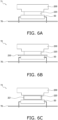
- FIG. 6A is a side view of a first printed wiring board assembly 71.
- the first heat transfer member 220 is interposed between the active filter module 50 and the heat sink 200.
- FIG. 6B is a side view of a second printed wiring board assembly 72.
- the first heat transfer member 220 and an insulating sheet 230 are interposed between the active filter module 50 and the heat sink 200.
- FIG. 6C is a side view of a third printed wiring board assembly 73.
- the first heat transfer member 220 subjected to alumite treatment is interposed between the active filter module 50 and the heat sink 200.
- the alumite treatment is surface treatment in which an aluminum surface is electrolyzed with an anode to generate an oxide film. Therefore, a surface of the first heat transfer member 220 is covered with an oxide film 221.
- FIG. 7 is a graph for comparing parasitic capacitances between the active filter module 50 and the heat sink 200 in the first printed wiring board assembly 71, the second printed wiring board assembly 72, and the third printed wiring board assembly 73.
- the parasitic capacitance is the largest in 62 of the first printed wiring board assembly 71, and is less in order of 50 of the third printed wiring board assembly 73 and 21 of the second printed wiring board assembly 72.
- the noise component passes through the carrier filter 53, which reduces the noise component and improves deterioration of EMI during operation of the active filter module 50.
- the first heat transfer member 220 subjected to the alumite treatment in FIG. 6C is interposed between the active filter module 50 and the heat sink 200 to suppress the common mode noise.
- the printed wiring board 70 is a multilayer printed wiring board having a plurality of conductive pattern layers laminated with an insulator layer interposed in between.
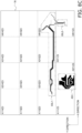
- FIGS. 8A , 8B , 8C , and 8D are plan views of the printed wiring board 70 illustrating a part of a conductive pattern of each of a first layer Z 1, a second layer Z2, a third layer Z3, and a fourth layer Z4 of the printed wiring board 70.
- each layer is sectioned into 16 regions in plan view, and each region is denoted by a reference sign indicating a position thereof.
- a region at an upper right end of the fourth layer Z4 in FIG. 8D in plan view is indicated as a region X4Y4Z4.
- FIGS. 8A , 8B , 8C , and 8D When the layers of FIGS. 8A , 8B , 8C , and 8D are laminated, regions having the same number after X and the same number after Y completely overlap with each other when viewed from the laminating direction.
- FIG. 9 is a plan view of the printed wiring board 70, illustrating a positional relationship of individual patterns when the first layer Z1, the second layer Z2, the third layer Z3, and the fourth layer Z4 are laminated and viewed from the first layer Z1 side toward the laminating direction.
- a low-voltage pattern for current detection is formed so as not to overlap with a high-voltage pattern formed in another layer when viewed from the laminating direction.
- a first-A low-voltage pattern 41L is formed in a region X4Y3Z1.
- the first-A low-voltage pattern 41L is a conductive pattern to be used for detecting a current of the inverter module 30.
- the current of the inverter module 30 is detected via the current detection unit 33.
- a first-B low-voltage pattern 61L is formed in a region X2Y3Z1.
- the first-B low-voltage pattern 61L is a conductive pattern to be used for detecting a current of the active filter module 50.
- the current of the active filter module 50 is detected via the current detection unit 57.
- a first high-voltage pattern 61H is formed in regions X2Y4Z1, X3Y4Z1, X2Y3Z1, X3Y3Z1, and X3Y2Z1.
- the first high-voltage pattern 61H is a high-voltage line connecting the output side of the rectifier circuit 20 and an input side of the active filter circuit 60.
- a low-voltage pattern other than those for current detection and voltage detection is formed so as to overlap with a high-voltage pattern formed in another layer when viewed from the laminating direction.
- a second low-voltage pattern 42L is formed in a region X2Y1Z2.
- the second low-voltage pattern 42L is a low-voltage line to be used for transmitting an on/off signal of each relay for refrigerant control.
- a third-A high-voltage pattern 43H that is not the inverter circuit 40 and the active filter circuit 60 (for example, a high-voltage pattern of a switching power source circuit, an outdoor fan circuit, a refrigerant control circuit, a connection circuit to an indoor unit, and the like in a case of an air conditioner), and the second low-voltage pattern 42L and the third-A high-voltage pattern 43H partially overlap with each other as viewed in the laminating direction as illustrated in an R1 portion of FIG. 9 .
- a signal passing through the second low-voltage pattern 42L is subjected to noise removal by a CR filter before entering a microcomputer and a relay.
- a degree of freedom in designing the printed wiring board 70 is increased by allowing a part of the second low-voltage pattern 42L to overlap with the third-A high-voltage pattern 43H as viewed in the laminating direction.
- a second high-voltage pattern 52H is formed in regions X4Y2Z2 and X4Y1Z2.
- a high voltage to be supplied to the inverter circuit 40 and the active filter circuit 60 is supplied to the second high-voltage pattern 52H.
- a part of a low-voltage pattern other than those for current detection and voltage detection is formed so as to overlap with a high-voltage pattern formed in another layer when viewed from the laminating direction.
- a third-A low-voltage pattern 83L is formed in regions X1Y2Z3, X2Y2Z3, X3Y2Z3, and X4Y2Z3.
- the third-A low-voltage pattern 83L is a supply line for each output voltage (5 V, 15 V, and the like) generated by the switching power source 80.
- the second high-voltage pattern 52H exists in the region X4Y2Z2 of the second layer Z2 overlapping with the region X4Y2Z3 in which a part of the third-A low-voltage pattern 83L1 exists as viewed in the laminating direction, and the third-A low-voltage pattern 83L1 and the second high-voltage pattern 52H partially overlap with each other as viewed in the laminating direction, as illustrated in a portion R2 of FIG. 9 .
- a signal passing through the third-A low-voltage pattern 83L1 is subjected to noise removal by a CR filter before entering a microcomputer and a power module.
- a degree of freedom in designing the printed wiring board 70 is increased by allowing a part of the third-A low-voltage pattern 83L1 to overlap with the second high-voltage pattern 52H as viewed in the laminating direction.
- a third-B low-voltage pattern 83L2 is formed in a region X4Y1Z3.
- the third-B low-voltage pattern 83L2 is a low-voltage line to be used for transmitting an on/off signal of the main relay 93.
- the second high-voltage pattern 52H is exists in the region X4Y1Z2 of the second layer Z2 overlapping with the region X4Y1Z3 in which the third-B low-voltage pattern 83L2 exists as viewed in the laminating direction, and the third-B low-voltage pattern 83L2 and the second high-voltage pattern 52H partially overlap with each other as viewed in the laminating direction, as illustrated in the R3 portion of FIG. 9 .
- a signal passing through the third-B low-voltage pattern 83L2 is subjected to noise removal by a CR filter before entering a microcomputer and a relay.
- a degree of freedom in designing the printed wiring board 70 is increased by allowing a part of the third-B low-voltage pattern 83L2 to overlap with the second high-voltage pattern 52H as viewed in the laminating direction.
- the third-A high-voltage pattern 43H is formed in the region X2Y1Z3.
- the third-A high-voltage pattern 43H is a high-voltage line that is not the inverter circuit 40 and the active filter circuit 60 (for example, a high-voltage pattern of a switching power source circuit, an outdoor fan circuit, a refrigerant control circuit, a connection circuit to an indoor unit, and the like in a case of an air conditioner).
- low-voltage patterns for voltage detection and current detection are formed so as not to overlap with a high-voltage pattern formed in another layer when viewed from the laminating direction.
- a fourth-A low-voltage pattern 44L is formed in regions X3Y4Z4, X4Y4Z4, X4Y3Z4, and X4Y2Z4.
- the fourth-A low-voltage pattern 44L is a conductive pattern to be used for detecting a voltage of the inverter module 30.
- the voltage of the inverter module 30 is detected via the voltage detection unit 32.
- the region X4Y3Z1 of the first layer, the region X4Y3Z2 of the second layer Z2, and the region X4Y3Z3 of the third layer Z3 overlapping with the region X4Y3Z4 where a part of the fourth-A low-voltage pattern 44L exists as viewed in the laminating direction there is no high-voltage pattern that overlaps with a part of the fourth-A low-voltage pattern 44L as viewed in the laminating direction. Therefore, for example, even when the active filter circuit 60 operates, noise is not superimposed on the fourth-A low-voltage pattern 44L. Therefore, a voltage of the inverter circuit 40 can be accurately detected.
- a fourth-B low-voltage pattern 64L1 is formed in a region X3Y3Z4.
- the fourth-B low-voltage pattern 64L1 is a conductive pattern to be used for detecting a voltage of the active filter circuit 60.
- the voltage of the active filter circuit 60 is detected via the voltage detection unit 56.
- a part of the first high-voltage pattern 61H exists in the region X3Y3Z1 of the first layer Z1 overlapping with the region X3Y3Z4 where the fourth-B low-voltage pattern 64L1 exists as viewed in the laminating direction. Therefore, the fourth-B low-voltage pattern 64L1 overlaps with a part of the first high-voltage pattern 61H as viewed in the laminating direction.
- the first high-voltage pattern 61H is a high-voltage line connecting the output side of the rectifier circuit 20 and the input side of the active filter circuit 60, and both the first high-voltage pattern 61H and the fourth-B low-voltage pattern 64L1 belong to the active filter circuit 60.
- the low-voltage pattern for voltage or current detection may overlap with the high-voltage pattern in the laminating direction.
- a fourth-C low-voltage pattern 64L2 is formed in regions X3Y3Z4, X2Y2Z4, and X3Y2Z4.
- the fourth-C low-voltage pattern 64L2 is a conductive pattern to be used for detecting a current of the active filter circuit 60.
- the current of the active filter circuit 60 is detected via the U-phase current detection unit 58u and the W-phase current detection unit 58w.
- a part of the first high-voltage pattern 61H exists in the region X3Y2Z1 of the first layer Z1 overlapping with the region X3Y2Z4 where a part of the fourth-C low-voltage pattern 64L2 exists as viewed in the laminating direction. Therefore, the fourth-C low-voltage pattern 64L2 overlaps with a part of the first high-voltage pattern 61H as viewed in the laminating direction.
- the first high-voltage pattern 61H is a high-voltage line connecting the output side of the rectifier circuit 20 and the input side of the active filter circuit 60, and both the first high-voltage pattern 61H and the fourth-C low-voltage pattern 64L2 belong to the active filter circuit 60.
- FIG. 10 is a perspective view of the printed wiring board 70 when a long side direction of the printed wiring board 70 is an X direction, and a short side direction is a Y direction, and the printed wiring board 70 is virtually sectioned into three areas along the Y direction, that is, a first area 701, a second area 702, and a third area 703.
- the first area 701 is a range from a first end 70Ya, which is one end of the printed wiring board 70 in the Y direction, to a distance of about 1/3 of a length of the printed wiring board 70 in the Y direction.
- the third area 703 is a range from a second end 70Yb, which is another end in the Y direction of the printed wiring board 70, to a distance of 1/3 of the length of the printed wiring board 70 in the Y direction.
- the carrier filter 53 and the connection reactor 54 which can be said to be heavy objects, are arranged among the components constituting the active filter circuit 60.
- these heavy objects are referred to as a "first heavy object 601".
- a transformer 81 which can be said to be a heavy object among the components constituting the switching power source 80, is also arranged in the first area 701.
- the heavy object 601 of the active filter circuit 60 is arranged on one end side in the X direction of the first area 701
- the transformer 81 of the switching power source 80 is arranged on another end side in the X direction of the first area 701.
- the inverter module 30, the active filter module 50, and the power module 120 for fan are arranged along a long side direction (the X direction in FIG. 10 ) of the printed wiring board 70.
- the heat sink 200 has a shape extending along the X direction in FIG. 10 .
- the reactor 24 that can be said to be a heavy object among the components constituting the inverter circuit 40 is arranged.
- the heavy object is referred to as a "second heavy object 401".
- FIG. 11A is a front view of the printed wiring board 70 conveyed on a solder tank 730 and the first heavy object 601 and the second heavy object 401 having barycenters in the second area 702 of the printed wiring board 70 when viewed from a conveyance direction.
- FIG. 11B is a front view of the printed wiring board 70 conveyed on the solder tank 730, the first heavy object 601 having a barycenter in the first area 701 of the printed wiring board 70, and the second heavy object 401 having a barycenter in the third area 703, when viewed from a conveyance direction.
- the solder tank 730 is filled with molten solder 720.
- a conveyor 710 that moves the printed wiring board 70 is installed.
- the conveyor 710 sandwiches the first end 70Ya and the second end 70Yb of the printed wiring board 70, and conveys the printed wiring board 70 on a liquid surface of the molten solder 720 at a predetermined speed.
- the conveyance direction is a long side direction (the X direction in FIG. 10 ) of the printed wiring board 70.
- the liquid surface of the molten solder 720 is wavy due to a jet, and a soldering surface of the printed wiring board 70 is filled with the solder by the momentum.
- the printed wiring board 70 is deflected in a direction in which the second area 702 approaches the liquid surface of the solder 720.
- a barycenter of the first heavy object 601 is placed in the first area 701 having the first end 70Ya held by the conveyor 710, and a barycenter of the second heavy object 401 is placed in the third area 703 having the second end 70Yb held by the conveyor 710. Therefore, the second area 702 of the printed wiring board 70 is not deflected in a direction approaching the liquid surface of the solder 720.
- the printed wiring board 70 can smoothly move on the solder tank 730, and it is possible to suppress a state where solder is less likely to be attached.
- a printed wiring board assembly (see FIG. 10 ) in which electric components are soldered to the printed wiring board 70 is completed.
- the operator conveys the printed wiring board assembly to the next process, if the operator conveys the printed wiring board assembly by holding the first area 701 and the third area 703, unnecessary distortion is not generated in the printed wiring board 70.
- the inverter module 30 having a plurality of electrode pins, the active filter module 50, and the power module 120 for fan are arranged side by side in the long side direction (the X direction in FIG. 10 ), and these electrode pins are soldered to the printed wiring board 70. Therefore, the inverter module 30, the active filter module 50, and the power module 120 for fan serve as reinforcing members for the second area 702.
- the inverter module 30, the active filter module 50, and the power module 120 for fan are fastened with a screw to one heat sink 200 extending in the long side direction (the X direction in FIG. 10 ) of the second area 702, the second area 702 is indirectly reinforced.
- the second area 702 can withstand distortion and deflection since the second area 702 is reinforced by the inverter module 30, the active filter module 50, the power module 120 for fan, and the heat sink 200.
- an input of the AC power source 100 is connected to the connection points NU, NV, and NW of the active filter module 50, and the first capacitor 52 is connected between P and N terminals of the active filter module 50.
- the active filter module 50 itself receives an inrush current at a time of recovery from voltage drop or power failure of the power source or an inrush current due to power source frequency fluctuation during operation, so that the active filter module 50 is required to have durability against the inrush current.
- the active filter circuit has been optionally mounted on a dedicated board for the active filter circuit. Therefore, in order to cope with models of a plurality of horsepower levels with one type of active filter dedicated board, an active filter module having a large rated current has been mounted in accordance with a model of the highest horsepower. Therefore, the inrush current durability of the active filter module itself has been high, and it has not been necessary to worry about the inrush current durability of the active filter module.
- an ambient temperature of the printed wiring board 70 was set to - 35°C, 25°C, or 70°C, a power source voltage was set to 85% of the rated voltage, 100% of the rated voltage, or 115% of the rated voltage at each ambient temperature, and a power source frequency was switched from 50 Hz to 60 Hz or from 60 Hz to 50 Hz in each power source voltage to examine the inrush current durability.
- control voltage of the active filter module 50 was set to 15.0 V, 15.5 V, 16.0 V, and 16.5 V for confirmation.
- FIG. 12 is a table illustrating results of an inrush current durability experiment of the active filter module 50.
- the power source frequency was switched from 50 Hz to 60 Hz or from 60 Hz to 50 Hz at 15 V, which was a general control voltage of the active filter module 50, a large inrush current was generated in a compensation current of the active filter module 50 under any condition, and operation of the active filter module 50 was stopped or the active filter module 50 itself was damaged.
- control voltage of the active filter module 50 was 15.5 V
- operation of the active filter module 50 was stopped or the active filter module 50 itself was damaged, similarly to the case of 15 V
- control voltage was 16.0 V and 16.5 V
- operation of the active filter module 50 was not stopped, and the active filter module 50 itself was not damaged.
- the current durability is about 220% of the rated current when the control voltage is set to general 15 V, and the current durability is 250% or more of the rated current when the control voltage is set to 16 V or more.
- the current durability tends to increase.
- control voltage of the active filter module 50 was set to 16.5 V in consideration of a margin.
- the control voltage of the active filter module 50 is set not to general 15 V but to 16.5 V higher than that.
- the inrush current durability of the active filter module 50 itself is increased, and the active filter module 50 is prevented from being broken due to an inrush current at a time of recovery from voltage drop or power failure of the power source or power source frequency fluctuation during operation.
- a disadvantage of intentionally increasing the control voltage of the active filter module 50 is that a short-circuit durability time of the active filter module 50 is shortened.
- an upper limit value of the control voltage of the active filter module 50 is 22 V, it is preferable to limit the control voltage to 18 V in consideration of the short-circuit durability time.
- the control voltage of the active filter module 50 may be increased to 20 V at the expense of the short short-circuit durability time.
- control voltage of the active filter module 50 is preferably 16 V to 20 V
- output lines extend individually from the connection points NU, NV, and NW of the inverter module 30 toward the drive coils Lu, Lv, and Lw of the corresponding phases.
- the inverter module 30 when the inverter module 30 is short-circuited, not only the inverter circuit 40 but also the compressor is damaged. Therefore, the inverter module 30 needs to have durability against short-circuit in order to prevent breakage of the compressor even when the inverter module 30 is short-circuited.
- control voltage of the inverter module 30 is preferably set to 14.5 V so that the short-circuit durability time becomes longer than that of the active filter module 50.
- the inverter circuit 40 since the inverter circuit 40 is connected to a downstream side of the rectifier circuit 20 when viewed from the AC power source side, the inverter module 30 does not directly receive an input current at a time of recovery from voltage drop or power failure of the power source and an inrush current due to power source frequency fluctuation during operation. Therefore, the inverter module 30 is not required to have inrush current durability as high as that of the active filter module 50. Therefore, a lower limit value of the control voltage of the inverter module 30 may be, for example, 13 V
- a second heat transfer member 250 may be interposed between the inverter module 30 and the heat sink 200.
- an effect of increasing an impedance between the inverter module 30 and the heat sink 200 by the second heat transfer member 250 may be smaller than an effect of increasing an impedance between the active filter module 50 and the heat sink 200 by the first heat transfer member 220.
- Patent Literature 1 WO 2017-115431
Landscapes
- Engineering & Computer Science (AREA)
- Power Engineering (AREA)
- Inverter Devices (AREA)
- Amplifiers (AREA)
- Polarising Elements (AREA)
Abstract
Description
- The present invention relates to a power conversion device including an active filter circuit.
- As means for suppressing a harmonic current generated in a power conversion device, for example, an active filter circuit as disclosed in Patent Literature 1 (
WO 2017-115431 ) is widely known. - Conventionally, a mounting board of an active filter circuit is a board different from a mounting board of an inverter circuit constituting a DC-AC conversion unit of a power conversion device, which causes an increase in size and an increase in cost of the power conversion device.
- Therefore, there are problems of space saving, component saving, and cost reduction of the power conversion device.
- A power conversion device according to a first aspect includes an active filter circuit, an inverter circuit, and one printed wiring board. The active filter circuit is connected in parallel between an AC power source and a rectifier circuit, and generates a compensation current for suppressing a harmonic current. The rectifier circuit rectifies AC power of the AC power source into DC power. The inverter circuit converts DC power outputted from the rectifier circuit into AC power having a predetermined frequency. The active filter circuit and the inverter circuit are mounted on one printed wiring board.
- In this power conversion device, the power conversion device can be reduced in size, weight, and cost, by mounting the active filter circuit and the inverter circuit on one printed wiring board.
- A power conversion device according to a second aspect is the power conversion device according to the first aspect, in which the printed wiring board is a multilayer printed wiring board. The multilayer printed wiring board has a plurality of conductive pattern layers laminated with an insulator layer interposed in between. The printed wiring board includes a first layer and a second layer. The first layer forms a first low-voltage pattern for detecting a current or a voltage of the active filter circuit. The second layer forms a high-voltage pattern of the inverter circuit. The first low-voltage pattern does not overlap with the high-voltage pattern as viewed in a laminating direction.
- In this power conversion device, the first low-voltage pattern of the active filter circuit does not overlap with the high-voltage pattern of the inverter circuit as viewed in the laminating direction. Therefore, even when the inverter circuit operates, noise is less likely to be superimposed on the first low-voltage pattern of the active filter circuit. Therefore, the current or the voltage of the active filter circuit is accurately detected.
- A power conversion device according to a third aspect is the power conversion device according to the second aspect, in which the first layer further forms a second low-voltage pattern belonging to the active filter circuit, separately from the first low-voltage pattern. A part of the second low-voltage pattern overlaps with the high-voltage pattern as viewed in the laminating direction.
- In this power conversion device, even if noise is superimposed on the second low-voltage pattern irrelevant to detection of the current or the voltage of the active filter circuit, detection accuracy of the current or the voltage is not affected. Therefore, by allowing a part of the second low-voltage pattern to overlap with the high-voltage pattern as viewed in the laminating direction, a degree of freedom in designing the printed wiring board is increased.
- A power conversion device according to a fourth aspect is the power conversion device according to the first aspect, in which the printed wiring board is a multilayer printed wiring board. The multilayer printed wiring board has a plurality of conductive pattern layers laminated with an insulator layer interposed in between. The printed wiring board includes a first layer and a second layer. The first layer forms a first low-voltage pattern for detecting a current or a voltage of the inverter circuit. The second layer forms a high-voltage pattern of the active filter circuit. The first low-voltage pattern does not overlap with the high-voltage pattern as viewed in a laminating direction.
- In this power conversion device, the first low-voltage pattern of the inverter circuit does not overlap with the high-voltage pattern of the active filter circuit as viewed in the laminating direction. Therefore, even when the active filter circuit operates, noise is not superimposed on the first low-voltage pattern of the inverter circuit. Therefore, the current or the voltage of the inverter circuit is accurately detected.
- A power conversion device according to a fifth aspect is the power conversion device according to the fourth aspect, in which the first layer further forms a second low-voltage pattern belonging to the inverter circuit, separately from the first low-voltage pattern. A part of the second low-voltage pattern overlaps with the high-voltage pattern as viewed in the laminating direction.
- In this power conversion device, even if noise is superimposed on the second low-voltage pattern irrelevant to detection of the current or the voltage of the inverter circuit, detection accuracy of the current or the voltage is not affected. Therefore, by allowing a part of the second low-voltage pattern to overlap with the high-voltage pattern as viewed in the laminating direction, a degree of freedom in designing the printed wiring board is increased.
- A power conversion device according to a sixth aspect is the power conversion device according to any one of the first to fifth aspects, and further includes one switching power source circuit mounted on the printed wiring board. The active filter circuit and the inverter circuit receive power supply from the switching power source circuit.
- In this power conversion device, since it is not necessary for each of the active filter circuit and the inverter circuit to individually include a switching power source circuit, the power conversion device can be reduced in size, weight, and cost.
- A power conversion device according to a seventh aspect is the power conversion device according to the sixth aspect, in which mounting areas of the switching power source circuit, the active filter circuit, and the inverter circuit in the printed wiring board are separated. Circuit areas of the switching power source circuit, the active filter circuit, and the inverter circuit in the printed wiring board are also separated.
- In this power conversion device, a configuration is realized in which the first low-voltage pattern for detecting a current or a voltage does not overlap with the high-voltage pattern as viewed in the laminating direction.
- A power conversion device according to an eighth aspect is the power conversion device according to any one of the first to seventh aspects, and further includes a capacitor that smooths output power of the rectifier circuit, and a current-limiting circuit that limits a current flowing through the capacitor. The active filter circuit includes a first switching circuit that generates a compensation current for suppressing a harmonic current, and a first capacitor that smooths output power of the first switching circuit. The current-limiting circuit is also used as a current-limiting circuit that limits a current flowing through the first capacitor of the active filter circuit.
- In this power conversion device, since it is not necessary for the active filter circuit to individually include a current-limiting circuit, the power conversion device can be reduced in size, weight, and cost.
- A power conversion device according to a ninth aspect is the power conversion device according to the eighth aspect, in which the active filter circuit further includes a first power module that incorporates the first switching circuit in one package. The inverter circuit includes: a second power module that incorporates, in one package, a second switching circuit that converts DC power into AC power having a predetermined frequency; and a cooler that cools the second power module. The cooler is also used as a cooler that cools the first power module.
- In this power conversion device, since the first power module and the second power module can be cooled by one cooler, the power conversion device can be reduced in size, weight, and cost.
- A power conversion device according to a 10th aspect is the power conversion device according to any one of the first to eighth aspects, in which the active filter circuit includes a first heavy object that is an electric component. The inverter circuit includes a second heavy object that is an electric component. When the printed wiring board is sectioned into a first area, a second area, and a third area sequentially aligned in a predetermined first direction, the first heavy object is arranged in the first area, and the second heavy object is arranged in the third area.
- The inverter circuit and the active filter circuit include relatively heavy electrical components that can be said to be heavy objects. Therefore, when the inverter circuit and the active filter circuit are mounted on one printed wiring board, distortion and deflection are likely to occur in the printed wiring board if such heavy objects are biased in one area, which causes a failure.
- However, in this power conversion device, the heavy objects are mounted so as to sandwich the area where a power module is mounted. Therefore, the heavy objects are prevented from being biased to one area, and distortion and deflection are less likely to occur in the printed wiring board.
- A power conversion device according to an 11th aspect is the power conversion device according to the 10th aspect, in which the active filter circuit includes a first power module that generates a compensation current for suppressing a harmonic current. The inverter circuit includes a second power module that converts DC power into AC power having a predetermined frequency. At least one of the first power module or the second power module is arranged in the second area.
- In this power conversion device, since the second area is reinforced by mounting at least one power module, it is not necessary to newly add a reinforcing member.
- A power conversion device according to a 12th aspect is the power conversion device according to the 11th aspect, in which both the first power module and the second power module are arranged in the second area.
- In this power conversion device, since the second area is reinforced by mounting two power modules, it is not necessary to newly add a reinforcing member.
- A power conversion device according to a 13th aspect is the power conversion device according to the 11th or 12th aspect, and further includes a cooler. The cooler is attached to the first power module and the second power module, and cools the first power module and the second power module.
- In this power conversion device, two power modules are mounted in the second area, and the two power modules are further reinforced by being mechanically connected by the cooler. Therefore, it is not necessary to newly add a reinforcing member.
- A power conversion device according to a 14th aspect is the power conversion device according to the 13th aspect, in which the first power module and the second power module are arranged along a second direction orthogonal to the first direction. The cooler has a shape extending along the second direction.
- In this power conversion device, since the cooler having the shape extending along the second direction is attached to both power modules of the first power module and the second power module arranged along the second direction, strength of the second area in the second direction is enhanced. Here, the strength in the second direction is bending strength when the printed wiring board is regarded as a beam extending in the second direction.
- A power conversion device according to a 15th aspect is the power conversion device according to any one of the 10th to 14th aspects, in which at least one of the first heavy object or the second heavy object is a reactor.
- The reactor is heavier and higher than the first power module and the second power module, and an operator can quickly recognize that the reactor is a heavy object. Therefore, in this power conversion device, the reactor is mounted in the first area and the third area closer to an end of the printed wiring board than the second area, so that the operator naturally holds near the heavy object where the reactor is present when carrying the printed wiring board. This results in preventing distortion and deflection of the printed wiring board.
- A power conversion device according to a 16th aspect is the power conversion device according to any one of the 10th to 15th aspects, in which when at least one of the first heavy object or the second heavy object includes a plurality of components, the plurality of components are arranged in the second direction orthogonal to the first direction.
- When the individual heavy objects are concentrated in one place in each area, if a held spot when the printed wiring board is held is away from the individual heavy objects, a stress acting on the held spot increases.
- However, in this power conversion device, individual components of the first heavy object are arranged along the second direction of the first area of the printed wiring board, and the second heavy object is arranged along the second direction of the third area. Therefore, when the operator holds the printed wiring board, the stress acting on the held spot becomes smaller than that of the former case. This results in suppressing distortion and deflection of the printed wiring board.
- A power conversion device according to a 17th aspect is the power conversion device according to any one of the 10th to 16th aspects, in which the first area is in a distance within 1/3 of a length of the printed wiring board in the first direction, from a first end that is one end of the printed wiring board in the first direction. The third area is in a distance within 1/3 of the length of the printed wiring board in the first direction from a second end that is another end of the printed wiring board in the first direction.
- In this power conversion device, since the operator holds an end side when carrying the printed wiring board, the operator inevitably holds the first area or the third area where heavy objects are present. This results in preventing distortion and deflection of the printed wiring board.
- A power conversion device according to an 18th aspect is the power conversion device according to any one of the 10th to 17th aspects, in which mounting of the first heavy object and the second heavy object on the printed wiring board is realized when the printed wiring board on which the first heavy object and the second heavy object are placed passes through a solder flow tank along the second direction orthogonal to the first direction.
- In this power conversion device, the heavy objects pass through the solder flow tank along the second direction while being placed in the first area and the third area closer to an end of the printed wiring board than the second area. Therefore, the heavy objects are to be located on a holding portion side where an end of the printed wiring board is held, and distortion and deflection of the printed wiring board are prevented. This results in preventing soldering failure.
- A power conversion device according to a 19th aspect is the power conversion device according to any one of the first to eighth aspects, in which the active filter circuit includes a first power module. The first power module generates a compensation current for suppressing a harmonic current. The inverter circuit includes a second power module. The second power module converts DC power into AC power having a predetermined frequency. The power conversion device further includes a cooler and a first heat transfer member. The cooler is attached to the first power module and the second power module, and cools the first power module and the second power module. The first heat transfer member is arranged between the first power module and the cooler, and increases an impedance between the first power module and the cooler.
- In this power conversion device, since the impedance between the first power module and the cooler is increased by the first heat transfer member, a parasitic capacitance between the first power module and the cooler is reduced. As a result, a ground impedance of the cooler increases, a noise component passes through an existing noise filter, the noise component is reduced, and deterioration of EMI (a noise terminal voltage) during operation of the active filter circuit is suppressed.
- A power conversion device according to a 20th aspect is the power conversion device according to the 19th aspect, in which a thickness of the first heat transfer member is determined based on a potential difference between a terminal of the first power module and the cooler.
- In this power conversion device, since the thickness of the first heat transfer member is determined based on a physical quantity such as a potential difference between the terminal of the first power module and the cooler, the thickness of the first heat transfer member is appropriately set without excess or deficiency.
- A power conversion device according to a 21th aspect is the power conversion device according to the 19th or 20th aspect, in which a ground impedance of the first heat transfer member is adjusted by surface treatment on the first heat transfer member.
- In this power conversion device, since the ground impedance can be adjusted by the surface treatment on the first heat transfer member, it is possible to adjust the ground impedance while maintaining a heat transfer property of the first heat transfer member without requiring other members.
- A power conversion device according to a 22th aspect is the power conversion device according to any one of the 19th to 21th aspects, in which the cooler includes a cooling portion and a heat absorbing portion. The heat absorbing portion transfers heat from the first power module and the second power module to the cooling portion. The heat absorbing portion includes a heat absorbing surface surrounded by a long side parallel to a longitudinal direction of the cooling portion and a short side orthogonal to the longitudinal direction. The first power module and the second power module are attached to the heat absorbing surface of the heat absorbing portion. The first power module and the second power module are both rectangular parallelepipeds. A length of a short side of the first power module is equal to or more than a short side of the heat absorbing surface and equal to or less than a short side of the second power module.
- Since the first power module of the active filter circuit is smaller in package than the second power module of the inverter circuit, a distance between a terminal of the first power module and the heat absorbing portion becomes short when the first power module is attached to the heat absorbing portion of the cooler, which is more disadvantageous than the second power module in terms of a creepage distance and a spatial distance. In this power conversion device, since there is the first heat transfer member that increases the impedance between the first power module and the cooler, the disadvantage can be overcome.
- A power conversion device according to a 23th aspect is the power conversion device according to any one of the 19th to 22th aspects, and further includes a second heat transfer member. The second heat transfer member is arranged between the second power module and the cooler. An effect of increasing an impedance between the second power module and the cooler by the second heat transfer member is smaller than an effect of increasing the impedance between the first power module and the cooler by the first heat transfer member.
- In this power conversion device, a noise component of the inverter circuit can be reduced by the existing noise filter circuit. Therefore, the effect of increasing the impedance between the second power module and the cooler by the second heat transfer member may be smaller than the effect of increasing the impedance between the first power module and the cooler by the first heat transfer member. Therefore, since the existing noise filter circuit does not need to be strong, the size does not increase.
- A power conversion device according to a 24th aspect is the power conversion device according to any one of the first to eighth aspects, in which the active filter circuit includes a first power module. The first power module incorporates, in one package, a plurality of switching elements that generate a compensation current for suppressing a harmonic current and a control circuit that controls the switching elements. A control voltage of the first power module is 16.0 V or more.
- The active filter circuit is connected in parallel between the AC power source and the rectifier circuit, and the first power module receives an input current at a time of recovery from voltage drop or power failure of the power source and an inrush current due to power source frequency fluctuation during operation. Therefore, the first power module is required to have durability against inrush current.
- In this power conversion device, by setting the control voltage of the first power module to 16.0 V or more, which is higher than general 15 V, inrush current durability of the switching element is enhanced, which can increase breakdown durability of the switching element.
- A power conversion device according to a 25th aspect is the power conversion device according to the 24th aspect, in which the control voltage of the first power module is 16.5 V
- A power conversion device according to a 26th aspect is the power conversion device according to the 24th or 25th aspect, and further includes an inverter circuit. The inverter circuit includes a second power module. The second power module incorporates, in one package, a plurality of switching elements that convert DC power into AC power of a predetermined frequency and a control circuit that controls the switching elements. The control voltage of the second power module is smaller than the control voltage of the first power module.
- The inverter circuit is connected to a downstream side of the rectifier circuit when viewed from the AC power source side. Therefore, the second power module does not directly receive an input current at a time of recovery from voltage drop or power failure of the power source and an inrush current due to power source frequency fluctuation during operation, and the second power module is not required to have inrush current durability as high as that of the first power module.
- Therefore, the control voltage of the second power module can be made smaller than the control voltage of the first power module.
- A power conversion device according to a 27th aspect is the power conversion device according to the 26th aspect, in which a control voltage of the second power module is 15.5 V or less.
-
-
FIG. 1 is a circuit diagram illustrating a configuration of a power conversion device according to an embodiment of the present disclosure. -
FIG. 2 is a perspective view of a printed wiring board on which components are mounted. -
FIG. 3 is a plan view of a state in which a heat sink illustrated inFIG. 2 is reversed rightward by 180° around a right end in front view. -
FIG. 4 is a perspective view of the heat sink and an active filter module illustrated inFIG. 3 as viewed from a front side. -
FIG. 5 is a common mode equivalent circuit. -
FIG. 6A is a side view of a first printed wiring board assembly. -
FIG. 6B is a side view of a second printed wiring board assembly. -
FIG. 6C is a side view of a third printed wiring board assembly. -
FIG. 7 is a graph for comparing parasitic capacitances between the active filter module and the heat sink in the first printed wiring board assembly, the second printed wiring board assembly, and the third printed wiring board assembly. -
FIG. 8A is a plan view of a printed wiring board, illustrating a part of a conductive pattern of a first layer of the printed wiring board. -
FIG. 8B is a plan view of the printed wiring board, illustrating a part of a conductive pattern of a second layer of the printed wiring board. -
FIG. 8C is a plan view of the printed wiring board, illustrating a part of a conductive pattern of a third layer of the printed wiring board. -
FIG. 8D is a plan view of the printed wiring board, illustrating a part of a conductive pattern of a fourth layer of the printed wiring board. -
FIG. 9 is a plan view of the printed wiring board, illustrating a positional relationship of individual patterns when the first layer, the second layer, the third layer, and the fourth layer are laminated and viewed from the first layer side toward a laminating direction. -
FIG. 10 is a perspective view of the printed wiring board when the printed wiring board is virtually sectioned into three areas, that is, a first area, a second area, and a third area along a Y direction with a long side direction of the printed wiring board as an X direction and a short side direction as the Y direction. -
FIG. 11A is a front view of the printed wiring board conveyed on a solder tank, and a first heavy object and a second heavy object having barycenters in the second area of the printed wiring board, when viewed from a conveyance direction. -
FIG. 11B is a front view of the printed wiring board conveyed on the solder tank, the first heavy object having a barycenter in the first area of the printed wiring board, and the second heavy object having a barycenter in the third area, when viewed from a conveyance direction. -
FIG. 12 is a table illustrating results of an inrush current durability experiment of the active filter module. -
FIG. 1 is a circuit diagram illustrating a configuration of apower conversion device 10 according to an embodiment of the present disclosure. InFIG. 1 , thepower conversion device 10 includes arectifier circuit 20, aninverter circuit 40, anactive filter circuit 60, a switchingpower source 80, and one printedwiring board 70. - The
rectifier circuit 20 rectifies AC power of anAC power source 100 into DC power. TheAC power source 100 outputs a three-phase AC. - The
inverter circuit 40 converts the DC power outputted from therectifier circuit 20 into AC power of a predetermined frequency, and supplies the AC power to a motor M. The motor M is a three-phase AC motor, and drives a compressor provided in a refrigerant circuit of an air conditioner, for example. - The
active filter circuit 60 is connected in parallel between theAC power source 100 and therectifier circuit 20 as a harmonic reduction device. Theactive filter circuit 60 compensates for a harmonic current having a phase opposite to a harmonic current generated in theinverter circuit 40 on the basis of a current value flowing through theinverter circuit 40 and detected by acurrent detection unit 33, to reduce a harmonic current flowing from theinverter circuit 40 to a power source line. - A rectification unit 21 is configured in a bridge shape by six diodes D0a, D0b, D1a, D1b, D2a, and D2b. Specifically, the diodes D0a and D0b, D1a and D1b, and D2a and D2b are connected in series with each other.
- Individual cathode terminals of the diodes D0a, D1a, and D2a are connected to a positive side terminal of a smoothing
capacitor 22, and function as a positive side output terminal of therectifier circuit 20. - Individual anode terminals of the diodes D0b, D1b, and D2b are connected to a negative terminal of the smoothing
capacitor 22, and function as a negative output terminal of therectifier circuit 20. - A connection point of the diode D0a and the diode D0b is connected to one pole (U phase) of the three-phase
AC power source 100. A connection point of the diode D1a and the diode D1b is connected to another pole (V phase) of the three-phaseAC power source 100. A connection point of the diode D2a and the diode D2b is connected to a remaining one pole (W phase) of the three-phaseAC power source 100. - The
rectifier circuit 20 rectifies AC power outputted from the three-phaseAC power source 100 to generate DC power, and supplies the DC power to the smoothingcapacitor 22. - The
inverter circuit 40 includes areactor 24, the smoothingcapacitor 22, aninverter module 30, avoltage detection unit 32, thecurrent detection unit 33, and aninverter microcomputer 35. - The
reactor 24 has one end connected to a positive output terminal of therectifier circuit 20 and another end connected to a positive input terminal of the smoothingcapacitor 22. - The smoothing
capacitor 22 has one end connected to the positive output terminal of therectifier circuit 20 and another end connected to the negative output terminal of therectifier circuit 20. The smoothingcapacitor 22 smooths a voltage rectified by therectifier circuit 20. - The voltage smoothed by the smoothing
capacitor 22 is supplied to theinverter circuit 40 connected to an output side of the smoothingcapacitor 22. - While examples of the capacitor include an electrolytic capacitor, a film capacitor, and a tantalum capacitor, a film capacitor is adopted as the smoothing
capacitor 22 in the present embodiment. - The
reactor 24 and the smoothingcapacitor 22 constitute an LC filter. An inductance of thereactor 24 and a capacitance of the smoothing capacitor 23 are set such that the LC filter attenuates a current component having a frequency same as a frequency of a carrier used to generate a control signal of theinverter circuit 40. Therefore, a current component having the same frequency as the carrier frequency is suppressed from flowing out to theAC power source 100. - The
inverter module 30 incorporates a switchingcircuit 25 and acontrol circuit 26, and is formed into one package. - The switching
circuit 25 includes a plurality of switching elements that convert DC power into AC power of a predetermined frequency. Thecontrol circuit 26 controls the switching elements. - In the switching
circuit 25, three upper and lower arms individually corresponding to U-phase, V-phase, and W-phase drive coils Lu, Lv, and Lw of the motor M are connected in parallel to each other and to the output side of the smoothingcapacitor 22. - In
FIG. 1 , the switchingcircuit 25 includes a plurality of insulated gate bipolar transistors (IGBTs, hereinafter, simply referred to as transistors) Q3a, Q3b, Q4a, Q4b, Q5a, and Q5b, and a plurality of reflux diodes D3a, D3b, D4a, D4b, D5a, and D5b. - The transistors Q3a and Q3b, the transistors Q4a and Q4b, and the transistors Q5a and Q5b are respectively connected in series each other to constitute each upper and lower arms, and output wires extend from each connection points NU, NV, and NW thus formed to the drive coils Lu, Lv, and Lw for the corresponding phases.
- The diodes D3a to D5b are respectively connected in parallel with the transistors Q3a to Q5b with a collector terminal of each transistor connected to a cathode terminal of the corresponding diode and an emitter terminal of each transistor connected to an anode terminal of the corresponding diode. These transistors and the corresponding diodes, which are respectively connected in parallel, constitute a switching element.
- The switching
circuit 25 generates a drive voltage for driving the motor M, by applying a DC voltage from the smoothingcapacitor 22 and turning on and off each of the transistors Q3a to Q5b at a timing instructed by thecontrol circuit 26. This drive voltage is outputted from each of the connection points NU, NV, and NW of each of the transistors Q3a and Q3b, Q4a and Q4b, and Q5a and Q5b to the drive coils Lu, Lv, and Lw of the motor M. - The
control circuit 26 changes on and off states of each of the transistors Q3a to Q5b of the switchingcircuit 25 on the basis of a command voltage from theinverter microcomputer 35. - Specifically, the
control circuit 26 generates gate control voltages Gu, Gx, Gv, Gy, Gw, and Gz such that a pulse drive voltage having any duty ratio is outputted from the switchingcircuit 25 to the motor M. The duty ratio is determined by theinverter microcomputer 35. - The gate control voltages Gu, Gx, Gv, Gy, Gw, and Gz thus generated are respectively applied to gate terminals of the transistors Q3a, Q3b, Q4a, Q4b, Q5a, and Q5b.
- The
voltage detection unit 32 is connected to the output side of the smoothingcapacitor 22, and detects a voltage across terminals of the smoothingcapacitor 22. For example, thevoltage detection unit 32 is configured such that two resistances connected in series to each other are connected in parallel to the smoothingcapacitor 22, and a voltage across terminals of the smoothingcapacitor 22 is divided. A voltage value at a connection point between the two resistances is inputted to theinverter microcomputer 35. - The
current detection unit 33 is connected between the smoothingcapacitor 22 and the switchingcircuit 25, and to a negative-side output terminal of the smoothingcapacitor 22. After the motor M is activated, thecurrent detection unit 33 detects a motor current flowing through the motor M as a total value of currents for three phases. - The
current detection unit 33 may include, for example, an amplifier circuit using a shunt resistance and an operational amplifier that amplifies a voltage across terminals of the resistance. The motor current detected by thecurrent detection unit 33 is inputted to theinverter microcomputer 35. - The
inverter microcomputer 35 is connected to thevoltage detection unit 32, thecurrent detection unit 33, and thecontrol circuit 26. In the present embodiment, theinverter microcomputer 35 drives the motor M in a rotor position sensorless method. Note that a sensor method may be adopted without limiting to the rotor position sensorless method. - Further, the
inverter microcomputer 35 also monitors a detection value of thevoltage detection unit 32, and performs protection control to turn off the transistors Q3a to Q5b when the detection value of thevoltage detection unit 32 exceeds a predetermined threshold value. - The
active filter circuit 60 includes anactive filter module 50, afirst capacitor 52, acarrier filter 53, aconnection reactor 54, anactive filter microcomputer 55, avoltage detection unit 56, acurrent detection unit 57, a U-phasecurrent detection unit 58u, and a W-phasecurrent detection unit 58w. - The
active filter module 50 incorporates a switchingcircuit 45 and acontrol circuit 46, and is formed into one package. - The switching
circuit 45 includes a plurality of switching elements that generate a compensation current for suppressing a harmonic current. - By controlling a switching operation with the
control circuit 46 to control a current flowing between theAC power source 100 and the switchingcircuit 45, the switchingcircuit 45 cancels a harmonic current flowing from theinverter circuit 40 to a power source line. - Since a configuration of the switching
circuit 45 is the same as the configuration of the switchingcircuit 25 of theinverter module 30, a transistor and a diode which are components are denoted by the same reference numerals as the transistor and the diode of the switchingcircuit 25 of theinverter module 30, and the description thereof is omitted. - The
control circuit 46 controls the switching elements. Since a configuration of thecontrol circuit 46 is also the same as the configuration of thecontrol circuit 26 of theinverter module 30, the same reference numerals as those of thecontrol circuit 26 of theinverter module 30 are given, and the description thereof is omitted. - The
first capacitor 52 is a capacitor that smooths output power of the switchingcircuit 45. - The
carrier filter 53 removes noise associated with switching of the switchingcircuit 45. Specifically, thecarrier filter 53 removes a high-frequency component of a compensation current generated by switching of the switchingcircuit 45. - The
connection reactor 54 interconnects the switchingcircuit 45 and a power source line. - The
active filter microcomputer 55 is connected to thevoltage detection unit 56, thecurrent detection unit 57, the U-phasecurrent detection unit 58u, the W-phasecurrent detection unit 58w, and thecontrol circuit 46. - Further, the
active filter microcomputer 55 sends a command voltage for switching on/off of each switching element of the switchingcircuit 45 to thecontrol circuit 46, on the basis of each detection value of thevoltage detection unit 56, thecurrent detection unit 57, the U-phasecurrent detection unit 58u, and the W-phasecurrent detection unit 58w. - The
voltage detection unit 56 is connected to an output side of thefirst capacitor 52, and detects a voltage across terminals of thefirst capacitor 52. For example, thevoltage detection unit 56 is configured such that two resistances connected in series to each other are connected in parallel to thefirst capacitor 52, and a voltage across terminals of thefirst capacitor 52 is divided. A voltage value at a connection point between the two resistances is inputted to theactive filter microcomputer 55. - The
current detection unit 57 is connected between thefirst capacitor 52 and the switchingcircuit 45, and to a negative-side output terminal of thefirst capacitor 52. Thecurrent detection unit 57 detects a bus current of the switchingcircuit 45. - The
current detection unit 57 may include, for example, an amplifier circuit using a shunt resistance and an operational amplifier that amplifies a voltage across terminals of the resistance. A current detected by thecurrent detection unit 57 is inputted to theactive filter microcomputer 55. - The U-phase
current detection unit 58u detects a compensation current flowing in the U phase. The W-phasecurrent detection unit 58w detects a compensation current flowing in the W phase. - The switching
power source 80 is connected to an output side of therectifier circuit 20, and supplies power to theinverter microcomputer 35 and thecontrol circuit 26 of theinverter module 30. Further, the switchingpower source 80 also supplies power to theactive filter microcomputer 55 and thecontrol circuit 46 of theactive filter module 50. - A connection position of the switching
power source 80 is not limited to the output side of therectifier circuit 20, and may be, for example, closer to theAC power source 100 than a current-limiting circuit 90. - The current-limiting circuit 90 includes a current-limiting
resistance 91, a current-limitingrelay 92, and amain relay 93. The current-limiting circuit 90 not only limits a current flowing through the smoothingcapacitor 22 but also serves as a current-limiting circuit that limits a current flowing through thefirst capacitor 52 of theactive filter circuit 60. Therefore, since theactive filter circuit 60 does not need to individually include a current-limiting circuit, thepower conversion device 10 can be reduced in size, weight, and cost. - The current-limiting
resistance 91 is connected on one power source line among three-phase power source lines connecting theAC power source 100 and therectifier circuit 20. - The current-limiting
resistance 91 is provided to gradually charge the smoothingcapacitor 22 and thefirst capacitor 52. A voltage of theAC power source 100 is applied to therectifier circuit 20 via the current-limitingresistance 91, and a current according to a resistance value of the current-limitingresistance 91 and an AC voltage of theAC power source 100 flows through the smoothingcapacitor 22 and thefirst capacitor 52 to gradually charge the smoothingcapacitor 22 and thefirst capacitor 52. - The current-limiting
relay 92 is connected in series with the current-limitingresistance 91 on a power source line to which the current-limitingresistance 91 is connected. - Between a contact points of the current-limiting
relay 92 is in a normally on state, and the current-limitingresistance 91 and therectifier circuit 20 are brought into a conductive state so as to bypass themain relay 93 when the motor M is activated. The current-limitingrelay 92 is turned off after the smoothingcapacitor 22 is appropriately charged. - The
main relay 93 is connected in parallel with the current-limitingresistance 91 and the current-limitingrelay 92 on a power source line to which the current-limitingresistance 91 and the current-limitingrelay 92 are connected, among three-phase power source lines connecting theAC power source 100 and therectifier circuit 20. Further, themain relay 93 is also connected to a power source line to which the current-limitingresistance 91 and the current-limitingrelay 92 are not connected. - When power of the
AC power source 100 is suddenly supplied to therectifier circuit 20, components such as the smoothingcapacitor 22 may be destroyed by an excessive inrush current. Therefore, normally, themain relay 93 turns off between the contact points and does not conduct a power source line connecting theAC power source 100 and therectifier circuit 20. - The
main relay 93 is turned on after the smoothingcapacitor 22 is appropriately charged and the current-limitingrelay 92 is turned off. -
FIG. 2 is a perspective view of the printedwiring board 70 on which components are mounted. InFIG. 2 , various components constituting theinverter circuit 40, theactive filter circuit 60, the switchingpower source 80, and the like illustrated inFIG. 1 are mounted on the printedwiring board 70. This eliminates necessity of a harness for connecting individual circuits, reducing in size and cost of thepower conversion device 10. - As illustrated in
FIG. 2 , aheat sink 200 is installed in theinverter module 30 in order to promote heat dissipation from the switchingcircuit 25 at a high temperature. -
FIG. 3 is a plan view of theheat sink 200 when theheat sink 200 illustrated inFIG. 2 is reversed rightward by 180° around a right end in a front view. InFIG. 3 , not only theinverter module 30 but also theactive filter module 50 and apower module 120 for fan are mounted on theheat sink 200. - The
heat sink 200 is also used as a cooler that cools theactive filter module 50 and thepower module 120 for fan. - Since the
inverter module 30, theactive filter module 50, and thepower module 120 for fan can be cooled by the oneheat sink 200, thepower conversion device 10 can be reduced in size, weight, and cost. - The
heat sink 200 includes a coolingportion 201 and aheat absorbing portion 203. To the coolingportion 201, a heat transfer tube through which a refrigerant flows is attached. However, in a case of an air cooling system in which a fan blows air to the coolingportion 201 to promote heat dissipation, the heat transfer tube is unnecessary. - The
heat sink 200 is grounded from theheat absorbing portion 203 via aground wire 190. Theheat absorbing portion 203 transfers heat from theinverter module 30, theactive filter module 50, and thepower module 120 for fan to the coolingportion 201. - The
heat absorbing portion 203 includes aheat absorbing surface 203a surrounded by a long side parallel to a longitudinal direction of the coolingportion 201 and a short side orthogonal to the longitudinal direction. Theinverter module 30, theactive filter module 50, and thepower module 120 for fan are attached to theheat absorbing surface 203a of theheat absorbing portion 203. - The
inverter module 30, theactive filter module 50, and thepower module 120 for fan are all rectangular parallelepipeds. - A length of a short side of the
active filter module 50 is equal to or more than a short side of theheat absorbing surface 203a and equal to or less than a short side of theinverter module 30. - Since the
active filter module 50 is smaller in package than theinverter module 30, a distance between a terminal of theactive filter module 50 and theheat absorbing portion 203 becomes short when theactive filter module 50 is attached to theheat absorbing portion 203, which is more disadvantageous than theinverter module 30 in terms of a creepage distance and a spatial distance. Therefore, a firstheat transfer member 220 that increases an impedance between theactive filter module 50 and theheat sink 200 is interposed to overcome the disadvantage. -
FIG. 4 is a perspective view of theheat sink 200 and theactive filter module 50 illustrated inFIG. 3 when viewed from a front side. InFIG. 4 , the firstheat transfer member 220 is arranged between theheat sink 200 and theactive filter module 50. - The first
heat transfer member 220 is made of aluminum or aluminum alloy. A function of the firstheat transfer member 220 is to adjust a height with respect to theinverter module 30 and to transfer heat of theactive filter module 50 to theheat sink 200. - As illustrated in
FIG. 3 , in the present embodiment, theheat sink 200 is also used as a heat sink that cools theinverter module 30, theactive filter module 50, and thepower module 120 for fan mounted on one printedwiring board 70. - The
inverter module 30, theactive filter module 50, and thepower module 120 for fan have different heights from a mounting surface of the printedwiring board 70, and theinverter module 30 has the highest height from the mounting surface of the printedwiring board 70 among the three modules. - Therefore, the
heat sink 200 is configured to be parallel to the mounting surface of the printedwiring board 70 with a height adjusting member interposed between theheat sink 200 and the heat dissipation surfaces of theactive filter module 50 and thepower module 120 for fan. - A height adjustment member arranged between the heat dissipation surface of the
active filter module 50 and theheat sink 200 is the firstheat transfer member 220. A thickness of the firstheat transfer member 220 is not simply determined by a facing distance between the heat dissipation surface of theactive filter module 50 and theheat sink 200. - The thickness of the first
heat transfer member 220 is determined after suitability is determined based on a physical quantity such as a potential difference between the terminal of theactive filter module 50 and theheat sink 200. - Therefore, when the thickness of the first
heat transfer member 220 is not appropriate from the viewpoint of the potential difference, the facing distance itself is also readjusted. This allows the thickness of the firstheat transfer member 220 to be appropriately set without excess or deficiency. - Since the first
heat transfer member 220 is interposed between the heat dissipation surface of theactive filter module 50 and theheat sink 200, heat must be efficiently transferred from theactive filter module 50 to theheat sink 200. Therefore, the firstheat transfer member 220 is made of a material having high heat conductivity (for example, "aluminum" or "aluminum alloy", "copper" or "copper alloy", "ceramic material", or the like). - In the present embodiment, aluminum or aluminum alloy is adopted as the first
heat transfer member 220. -
FIG. 5 is a common mode equivalent circuit. InFIG. 5 , a LISN is a noise measurement device and is not a component of the circuit ofFIG. 1 . - The
active filter module 50 cancels a harmonic component generated by theinverter module 30 by switching. - Since a parasitic capacitance is formed between the
active filter module 50 and theheat sink 200, common mode noise caused by a resonance frequency of theconnection reactor 54 during operation of theactive filter module 50 escapes from theactive filter module 50 to the earth through theheat sink 200, which may deteriorate EMI (a noise terminal voltage). - Examples of a countermeasure against the common mode noise include deviating the resonance frequency from a target frequency band of a noise terminal voltage by increasing a reactance value of the
connection reactor 54, or reinforcing thecarrier filter 53, but these lead to an increase in size of the printedwiring board 70 and an increase in size of electric components. - Therefore, in the present embodiment, by increasing a resistance value between the
active filter module 50 and theheat sink 200, a parasitic capacitance between theactive filter module 50 and theheat sink 200 is reduced, and the common mode noise is suppressed. -
FIG. 6A is a side view of a first printedwiring board assembly 71. InFIG. 6A , in the first printedwiring board assembly 71, the firstheat transfer member 220 is interposed between theactive filter module 50 and theheat sink 200. -
FIG. 6B is a side view of a second printedwiring board assembly 72. InFIG. 6B , in the second printedwiring board assembly 72, the firstheat transfer member 220 and an insulatingsheet 230 are interposed between theactive filter module 50 and theheat sink 200. -
FIG. 6C is a side view of a third printedwiring board assembly 73. InFIG. 6C , in the third printedwiring board assembly 73, the firstheat transfer member 220 subjected to alumite treatment is interposed between theactive filter module 50 and theheat sink 200. - The alumite treatment is surface treatment in which an aluminum surface is electrolyzed with an anode to generate an oxide film. Therefore, a surface of the first
heat transfer member 220 is covered with anoxide film 221. -
FIG. 7 is a graph for comparing parasitic capacitances between theactive filter module 50 and theheat sink 200 in the first printedwiring board assembly 71, the second printedwiring board assembly 72, and the third printedwiring board assembly 73. - In
FIG. 7 , the parasitic capacitance is the largest in 62 of the first printedwiring board assembly 71, and is less in order of 50 of the third printedwiring board assembly 73 and 21 of the second printedwiring board assembly 72. - When the parasitic capacitance between the
active filter module 50 and theheat sink 200 is large, a ground impedance of theheat sink 200 is small. Therefore, a noise component escapes through an earth path and does not pass through thecarrier filter 53, which deteriorates EMI when theactive filter module 50 operates. - On the other hand, when the parasitic capacitance between the
active filter module 50 and theheat sink 200 is small, the ground impedance of theheat sink 200 is large. Therefore, the noise component passes through thecarrier filter 53, which reduces the noise component and improves deterioration of EMI during operation of theactive filter module 50. - In the present embodiment, in consideration of cost effectiveness, the first
heat transfer member 220 subjected to the alumite treatment inFIG. 6C is interposed between theactive filter module 50 and theheat sink 200 to suppress the common mode noise. - The printed
wiring board 70 is a multilayer printed wiring board having a plurality of conductive pattern layers laminated with an insulator layer interposed in between. - In the present embodiment, when a surface on which various electrical components constituting the
inverter circuit 40, theactive filter circuit 60, and the switchingpower source 80 are mounted faces upward, conductive pattern layers of a first layer, a second layer, a third layer, and a fourth layer are laminated from upward to downward. -
FIGS. 8A ,8B ,8C , and8D are plan views of the printedwiring board 70 illustrating a part of a conductive pattern of each of afirst layer Z 1, a second layer Z2, a third layer Z3, and a fourth layer Z4 of the printedwiring board 70. - In
FIGS. 8A ,8B ,8C , and8D , for convenience of description, each layer is sectioned into 16 regions in plan view, and each region is denoted by a reference sign indicating a position thereof. - For example, in plan view of
FIGS. 8A ,8B ,8C , and8D , assuming that a position of a lower left end region is X1, the number after X increases by one every time the region is moved by one in the X direction. Further, every time the region is moved by one in the Y direction from Y1, the number after Y increases by one. - Further, every time the layer moves by one in the laminating direction from Z1, the number after Z increases by one. As a specific example, a region at an upper right end of the fourth layer Z4 in
FIG. 8D in plan view is indicated as a region X4Y4Z4. - When the layers of
FIGS. 8A ,8B ,8C , and8D are laminated, regions having the same number after X and the same number after Y completely overlap with each other when viewed from the laminating direction. -
FIG. 9 is a plan view of the printedwiring board 70, illustrating a positional relationship of individual patterns when the first layer Z1, the second layer Z2, the third layer Z3, and the fourth layer Z4 are laminated and viewed from the first layer Z1 side toward the laminating direction. - In the first layer Z1, a low-voltage pattern for current detection is formed so as not to overlap with a high-voltage pattern formed in another layer when viewed from the laminating direction.
- In
FIG. 8A , in the first layer Z1, a first-A low-voltage pattern 41L is formed in a region X4Y3Z1. The first-A low-voltage pattern 41L is a conductive pattern to be used for detecting a current of theinverter module 30. The current of theinverter module 30 is detected via thecurrent detection unit 33. - There is no high-voltage pattern in a region X4Y3Z2 of the second layer Z2, a region X4Y3Z3 of the third layer Z3, and a region X4Y3Z4 of the fourth layer Z4 overlapping with the region X4Y3Z1 where the first-A low-
voltage pattern 41L exists as viewed in the laminating direction. - For example, even when the
active filter circuit 60 operates, noise is not superimposed on the first-A low-voltage pattern 41L. Therefore, a current of theinverter circuit 40 can be accurately detected. - Further, in the first layer Z1, a first-B low-
voltage pattern 61L is formed in a region X2Y3Z1. The first-B low-voltage pattern 61L is a conductive pattern to be used for detecting a current of theactive filter module 50. The current of theactive filter module 50 is detected via thecurrent detection unit 57. - There is no high-voltage pattern in a region X2Y3Z2 of the second layer Z2, a region X2Y3Z3 of the third layer Z3, and a region X2Y3Z4 of the fourth layer Z4 overlapping with the region X2Y3Z1 where the first-B low-
voltage pattern 61L exists as viewed in the laminating direction. - For example, even when the
inverter circuit 40 operates, noise is not superimposed on the first-B low-voltage pattern 61L. Therefore, a current of theactive filter module 50 can be accurately detected. - Further, in the first layer Z1, a first high-
voltage pattern 61H is formed in regions X2Y4Z1, X3Y4Z1, X2Y3Z1, X3Y3Z1, and X3Y2Z1. The first high-voltage pattern 61H is a high-voltage line connecting the output side of therectifier circuit 20 and an input side of theactive filter circuit 60. - In the second layer, a low-voltage pattern other than those for current detection and voltage detection is formed so as to overlap with a high-voltage pattern formed in another layer when viewed from the laminating direction.
- In
FIG. 8B , in the second layer Z2, a second low-voltage pattern 42L is formed in a region X2Y1Z2. The second low-voltage pattern 42L is a low-voltage line to be used for transmitting an on/off signal of each relay for refrigerant control. - In a region X2Y1Z3 of the third layer Z3 overlapping with the region X2Y1Z2 where the second low-
voltage pattern 42L exists as viewed in the laminating direction, there is a third-A high-voltage pattern 43H that is not theinverter circuit 40 and the active filter circuit 60 (for example, a high-voltage pattern of a switching power source circuit, an outdoor fan circuit, a refrigerant control circuit, a connection circuit to an indoor unit, and the like in a case of an air conditioner), and the second low-voltage pattern 42L and the third-A high-voltage pattern 43H partially overlap with each other as viewed in the laminating direction as illustrated in an R1 portion ofFIG. 9 . - Therefore, a signal passing through the second low-
voltage pattern 42L is subjected to noise removal by a CR filter before entering a microcomputer and a relay. - As described above, for the second low-
voltage pattern 42L irrelevant to detection of a current or a voltage, a degree of freedom in designing the printedwiring board 70 is increased by allowing a part of the second low-voltage pattern 42L to overlap with the third-A high-voltage pattern 43H as viewed in the laminating direction. - Further, in the second layer Z2, a second high-
voltage pattern 52H is formed in regions X4Y2Z2 and X4Y1Z2. A high voltage to be supplied to theinverter circuit 40 and theactive filter circuit 60 is supplied to the second high-voltage pattern 52H. - In the third layer, a part of a low-voltage pattern other than those for current detection and voltage detection is formed so as to overlap with a high-voltage pattern formed in another layer when viewed from the laminating direction.
- In
FIG. 8C , in the third layer Z3, a third-A low-voltage pattern 83L is formed in regions X1Y2Z3, X2Y2Z3, X3Y2Z3, and X4Y2Z3. The third-A low-voltage pattern 83L is a supply line for each output voltage (5 V, 15 V, and the like) generated by the switchingpower source 80. - The second high-
voltage pattern 52H exists in the region X4Y2Z2 of the second layer Z2 overlapping with the region X4Y2Z3 in which a part of the third-A low-voltage pattern 83L1 exists as viewed in the laminating direction, and the third-A low-voltage pattern 83L1 and the second high-voltage pattern 52H partially overlap with each other as viewed in the laminating direction, as illustrated in a portion R2 ofFIG. 9 . - Therefore, a signal passing through the third-A low-voltage pattern 83L1 is subjected to noise removal by a CR filter before entering a microcomputer and a power module.
- As described above, for the third-A low-voltage pattern 83L1 irrelevant to the detection of the current or the voltage, a degree of freedom in designing the printed
wiring board 70 is increased by allowing a part of the third-A low-voltage pattern 83L1 to overlap with the second high-voltage pattern 52H as viewed in the laminating direction. - In
FIG. 8C , in the third layer Z3, a third-B low-voltage pattern 83L2 is formed in a region X4Y1Z3. The third-B low-voltage pattern 83L2 is a low-voltage line to be used for transmitting an on/off signal of themain relay 93. - The second high-
voltage pattern 52H is exists in the region X4Y1Z2 of the second layer Z2 overlapping with the region X4Y1Z3 in which the third-B low-voltage pattern 83L2 exists as viewed in the laminating direction, and the third-B low-voltage pattern 83L2 and the second high-voltage pattern 52H partially overlap with each other as viewed in the laminating direction, as illustrated in the R3 portion ofFIG. 9 . - Therefore, a signal passing through the third-B low-voltage pattern 83L2 is subjected to noise removal by a CR filter before entering a microcomputer and a relay.
- As described above, for the third-B low-voltage pattern 83L2 irrelevant to the detection of the current or the voltage, a degree of freedom in designing the printed
wiring board 70 is increased by allowing a part of the third-B low-voltage pattern 83L2 to overlap with the second high-voltage pattern 52H as viewed in the laminating direction. - Further, in the third layer Z3, the third-A high-
voltage pattern 43H is formed in the region X2Y1Z3. The third-A high-voltage pattern 43H is a high-voltage line that is not theinverter circuit 40 and the active filter circuit 60 (for example, a high-voltage pattern of a switching power source circuit, an outdoor fan circuit, a refrigerant control circuit, a connection circuit to an indoor unit, and the like in a case of an air conditioner). - In the fourth layer Z4, low-voltage patterns for voltage detection and current detection are formed so as not to overlap with a high-voltage pattern formed in another layer when viewed from the laminating direction.
- In
FIG. 8D , in the fourth layer Z4, a fourth-A low-voltage pattern 44L is formed in regions X3Y4Z4, X4Y4Z4, X4Y3Z4, and X4Y2Z4. The fourth-A low-voltage pattern 44L is a conductive pattern to be used for detecting a voltage of theinverter module 30. The voltage of theinverter module 30 is detected via thevoltage detection unit 32. - In the region X4Y3Z1 of the first layer, the region X4Y3Z2 of the second layer Z2, and the region X4Y3Z3 of the third layer Z3 overlapping with the region X4Y3Z4 where a part of the fourth-A low-
voltage pattern 44L exists as viewed in the laminating direction, there is no high-voltage pattern that overlaps with a part of the fourth-A low-voltage pattern 44L as viewed in the laminating direction. Therefore, for example, even when theactive filter circuit 60 operates, noise is not superimposed on the fourth-A low-voltage pattern 44L. Therefore, a voltage of theinverter circuit 40 can be accurately detected. - Further, in the fourth layer Z4, a fourth-B low-voltage pattern 64L1 is formed in a region X3Y3Z4. The fourth-B low-voltage pattern 64L1 is a conductive pattern to be used for detecting a voltage of the
active filter circuit 60. The voltage of theactive filter circuit 60 is detected via thevoltage detection unit 56. - A part of the first high-
voltage pattern 61H exists in the region X3Y3Z1 of the first layer Z1 overlapping with the region X3Y3Z4 where the fourth-B low-voltage pattern 64L1 exists as viewed in the laminating direction. Therefore, the fourth-B low-voltage pattern 64L1 overlaps with a part of the first high-voltage pattern 61H as viewed in the laminating direction. - However, the first high-
voltage pattern 61H is a high-voltage line connecting the output side of therectifier circuit 20 and the input side of theactive filter circuit 60, and both the first high-voltage pattern 61H and the fourth-B low-voltage pattern 64L1 belong to theactive filter circuit 60. - Therefore, there is no influence of noise generated when the fourth-B low-voltage pattern 64L1 overlaps with another high-voltage pattern as viewed in the laminating direction.
- Therefore, for example, even when the
inverter circuit 40 operates, noise is not superimposed on the fourth-B low-voltage pattern 64L. Therefore, a voltage of theactive filter circuit 60 can be accurately detected. - As described above, in the conductive patterns belonging to the same circuit, the low-voltage pattern for voltage or current detection may overlap with the high-voltage pattern in the laminating direction.
- As a modification, for example, a case is conceivable in which a low-voltage pattern for voltage or current detection belonging to the
inverter circuit 40 overlaps with a high-voltage pattern belonging to theinverter circuit 40 in the laminating direction. Even in such a case, there is no influence of noise generated in overlapping with another high-voltage pattern not belonging to theinverter circuit 40 as viewed in the laminating direction. - Further, in the fourth layer Z4, a fourth-C low-voltage pattern 64L2 is formed in regions X3Y3Z4, X2Y2Z4, and X3Y2Z4. The fourth-C low-voltage pattern 64L2 is a conductive pattern to be used for detecting a current of the
active filter circuit 60. The current of theactive filter circuit 60 is detected via the U-phasecurrent detection unit 58u and the W-phasecurrent detection unit 58w. - A part of the first high-
voltage pattern 61H exists in the region X3Y2Z1 of the first layer Z1 overlapping with the region X3Y2Z4 where a part of the fourth-C low-voltage pattern 64L2 exists as viewed in the laminating direction. Therefore, the fourth-C low-voltage pattern 64L2 overlaps with a part of the first high-voltage pattern 61H as viewed in the laminating direction. - However, the first high-
voltage pattern 61H is a high-voltage line connecting the output side of therectifier circuit 20 and the input side of theactive filter circuit 60, and both the first high-voltage pattern 61H and the fourth-C low-voltage pattern 64L2 belong to theactive filter circuit 60. - Therefore, there is no influence of noise generated when the fourth-C low-voltage pattern 64L2 overlaps with another high-voltage pattern as viewed in the laminating direction.
- Therefore, for example, even when the
inverter circuit 40 operates, noise is not superimposed on the fourth-C low-voltage pattern 64L2. Therefore, a current of theactive filter circuit 60 can be accurately detected. -
FIG. 10 is a perspective view of the printedwiring board 70 when a long side direction of the printedwiring board 70 is an X direction, and a short side direction is a Y direction, and the printedwiring board 70 is virtually sectioned into three areas along the Y direction, that is, afirst area 701, asecond area 702, and athird area 703. - The
first area 701 is a range from a first end 70Ya, which is one end of the printedwiring board 70 in the Y direction, to a distance of about 1/3 of a length of the printedwiring board 70 in the Y direction. - The
third area 703 is a range from a second end 70Yb, which is another end in the Y direction of the printedwiring board 70, to a distance of 1/3 of the length of the printedwiring board 70 in the Y direction. - In the
first area 701, thecarrier filter 53 and theconnection reactor 54, which can be said to be heavy objects, are arranged among the components constituting theactive filter circuit 60. For convenience of description, these heavy objects are referred to as a "firstheavy object 601". - Further, a
transformer 81, which can be said to be a heavy object among the components constituting the switchingpower source 80, is also arranged in thefirst area 701. - Further, in order to avoid local concentration of barycenters of the first
heavy object 601 of theactive filter circuit 60 and thetransformer 81 of the switchingpower source 80 also in thefirst area 701, theheavy object 601 of theactive filter circuit 60 is arranged on one end side in the X direction of thefirst area 701, and thetransformer 81 of the switchingpower source 80 is arranged on another end side in the X direction of thefirst area 701. - In the
second area 702 sandwiched between thefirst area 701 and thethird area 703, theinverter module 30, theactive filter module 50, and thepower module 120 for fan are arranged along a long side direction (the X direction inFIG. 10 ) of the printedwiring board 70. - To the
inverter module 30, theactive filter module 50, and thepower module 120 for fan, thecommon heat sink 200 is attached. Therefore, theheat sink 200 has a shape extending along the X direction inFIG. 10 . - In the
third area 703, thereactor 24 that can be said to be a heavy object among the components constituting theinverter circuit 40 is arranged. For convenience of description, the heavy object is referred to as a "secondheavy object 401". -
FIG. 11A is a front view of the printedwiring board 70 conveyed on asolder tank 730 and the firstheavy object 601 and the secondheavy object 401 having barycenters in thesecond area 702 of the printedwiring board 70 when viewed from a conveyance direction. - Further,
FIG. 11B is a front view of the printedwiring board 70 conveyed on thesolder tank 730, the firstheavy object 601 having a barycenter in thefirst area 701 of the printedwiring board 70, and the secondheavy object 401 having a barycenter in thethird area 703, when viewed from a conveyance direction. - In
FIGS. 11A and 11B , thesolder tank 730 is filled withmolten solder 720. At both ends of the opening of thesolder tank 730, aconveyor 710 that moves the printedwiring board 70 is installed. - The
conveyor 710 sandwiches the first end 70Ya and the second end 70Yb of the printedwiring board 70, and conveys the printedwiring board 70 on a liquid surface of themolten solder 720 at a predetermined speed. The conveyance direction is a long side direction (the X direction inFIG. 10 ) of the printedwiring board 70. - The liquid surface of the
molten solder 720 is wavy due to a jet, and a soldering surface of the printedwiring board 70 is filled with the solder by the momentum. - As illustrated in
FIG. 11A , in a case where a barycenter of the firstheavy object 601 and a barycenter of the secondheavy object 401 are placed in thesecond area 702 of the printedwiring board 70, the printedwiring board 70 is deflected in a direction in which thesecond area 702 approaches the liquid surface of thesolder 720. - When the deflection of the printed
wiring board 70 increases, not only the printedwiring board 70 cannot smoothly move on thesolder tank 730 but also solder is less likely to be attached. - On the other hand, in the present embodiment, as illustrated in
FIG. 11B , a barycenter of the firstheavy object 601 is placed in thefirst area 701 having the first end 70Ya held by theconveyor 710, and a barycenter of the secondheavy object 401 is placed in thethird area 703 having the second end 70Yb held by theconveyor 710. Therefore, thesecond area 702 of the printedwiring board 70 is not deflected in a direction approaching the liquid surface of thesolder 720. - Therefore, the printed
wiring board 70 can smoothly move on thesolder tank 730, and it is possible to suppress a state where solder is less likely to be attached. - Further, in a soldering process, a printed wiring board assembly (see
FIG. 10 ) in which electric components are soldered to the printedwiring board 70 is completed. When the operator conveys the printed wiring board assembly to the next process, if the operator conveys the printed wiring board assembly by holding thefirst area 701 and thethird area 703, unnecessary distortion is not generated in the printedwiring board 70. - On the other hand, when only one of the
first area 701 or thethird area 703 is inadvertently held, for example, when thethird area 703 is held such that the printedwiring board 70 is horizontal, a moment due to a weight of the firstheavy object 601 and thetransformer 81 in thefirst area 701 acts on thesecond area 702. This is not a preferable situation for the printedwiring board 70. - However, in the
second area 702, theinverter module 30 having a plurality of electrode pins, theactive filter module 50, and thepower module 120 for fan are arranged side by side in the long side direction (the X direction inFIG. 10 ), and these electrode pins are soldered to the printedwiring board 70. Therefore, theinverter module 30, theactive filter module 50, and thepower module 120 for fan serve as reinforcing members for thesecond area 702. - In addition, since the
inverter module 30, theactive filter module 50, and thepower module 120 for fan are fastened with a screw to oneheat sink 200 extending in the long side direction (the X direction inFIG. 10 ) of thesecond area 702, thesecond area 702 is indirectly reinforced. - As a result, even if the operator holds only one of the
first area 701 or thethird area 703, thesecond area 702 can withstand distortion and deflection since thesecond area 702 is reinforced by theinverter module 30, theactive filter module 50, thepower module 120 for fan, and theheat sink 200. - As illustrated in
FIG. 1 , in theactive filter circuit 60, an input of theAC power source 100 is connected to the connection points NU, NV, and NW of theactive filter module 50, and thefirst capacitor 52 is connected between P and N terminals of theactive filter module 50. - As a result, the
active filter module 50 itself receives an inrush current at a time of recovery from voltage drop or power failure of the power source or an inrush current due to power source frequency fluctuation during operation, so that theactive filter module 50 is required to have durability against the inrush current. - Conventionally, the active filter circuit has been optionally mounted on a dedicated board for the active filter circuit. Therefore, in order to cope with models of a plurality of horsepower levels with one type of active filter dedicated board, an active filter module having a large rated current has been mounted in accordance with a model of the highest horsepower. Therefore, the inrush current durability of the active filter module itself has been high, and it has not been necessary to worry about the inrush current durability of the active filter module.
- At this time, in order to integrate the
inverter circuit 40 and theactive filter circuit 60 with one printedwiring board 70 and reduce in size and cost, it is necessary to set theactive filter module 50 having an optimum rated current according to horsepower of an application model. - As an effect thereof, in comparison with a conventional product, the inrush current durability of the
active filter module 50 itself becomes low, and theactive filter module 50 may fail due to the inrush current. - Therefore, an experiment has been conducted to examine the inrush current durability in a case of using the
active filter module 50 having an optimum rated current according to the horsepower of the application model. - In the experiment, an ambient temperature of the printed
wiring board 70 was set to - 35°C, 25°C, or 70°C, a power source voltage was set to 85% of the rated voltage, 100% of the rated voltage, or 115% of the rated voltage at each ambient temperature, and a power source frequency was switched from 50 Hz to 60 Hz or from 60 Hz to 50 Hz in each power source voltage to examine the inrush current durability. - In any condition, the control voltage of the
active filter module 50 was set to 15.0 V, 15.5 V, 16.0 V, and 16.5 V for confirmation. -
FIG. 12 is a table illustrating results of an inrush current durability experiment of theactive filter module 50. InFIG. 12 , when the power source frequency was switched from 50 Hz to 60 Hz or from 60 Hz to 50 Hz at 15 V, which was a general control voltage of theactive filter module 50, a large inrush current was generated in a compensation current of theactive filter module 50 under any condition, and operation of theactive filter module 50 was stopped or theactive filter module 50 itself was damaged. - Next, when the control voltage of the
active filter module 50 was 15.5 V, operation of theactive filter module 50 was stopped or theactive filter module 50 itself was damaged, similarly to the case of 15 V - When the control voltage was 16.0 V and 16.5 V, operation of the
active filter module 50 was not stopped, and theactive filter module 50 itself was not damaged. - In a relationship between the control voltage of the
active filter module 50 and current durability, the current durability is about 220% of the rated current when the control voltage is set to general 15 V, and the current durability is 250% or more of the rated current when the control voltage is set to 16 V or more. When the control voltage of theactive filter module 50 is increased, the current durability tends to increase. - There is no problem in practical use as long as the durability against the current having the rated current ratio of 250% can be secured. Therefore, in the present embodiment, the control voltage of the
active filter module 50 was set to 16.5 V in consideration of a margin. - On the basis of the above experimental results, in the embodiment according to the present disclosure, the control voltage of the
active filter module 50 is set not to general 15 V but to 16.5 V higher than that. As a result, the inrush current durability of theactive filter module 50 itself is increased, and theactive filter module 50 is prevented from being broken due to an inrush current at a time of recovery from voltage drop or power failure of the power source or power source frequency fluctuation during operation. - Here, a disadvantage of intentionally increasing the control voltage of the
active filter module 50 is that a short-circuit durability time of theactive filter module 50 is shortened. - Therefore, although an upper limit value of the control voltage of the
active filter module 50 is 22 V, it is preferable to limit the control voltage to 18 V in consideration of the short-circuit durability time. - However, in the case of the
active filter circuit 60, even if the NU, NV, and NW terminals of theactive filter module 50 are short-circuited, damage remains only in theactive filter circuit 60 because the input of theAC power source 100 is connected to the NU, NV, and NW terminals of theactive filter module 50. Therefore, the damage is smaller than that in a situation where theinverter circuit 40 is damaged and the entire motor M needs to be replaced. - Therefore, in a case where the short-circuit tolerance of the
active filter module 50 is not important in theactive filter circuit 60, the control voltage of theactive filter module 50 may be increased to 20 V at the expense of the short short-circuit durability time. - Therefore, the control voltage of the
active filter module 50 is preferably 16 V to 20 V - For example, in a case where the motor M is a motor of a variable capacity compressor, as illustrated in
FIG. 1 , output lines extend individually from the connection points NU, NV, and NW of theinverter module 30 toward the drive coils Lu, Lv, and Lw of the corresponding phases. - Therefore, when the
inverter module 30 is short-circuited, not only theinverter circuit 40 but also the compressor is damaged. Therefore, theinverter module 30 needs to have durability against short-circuit in order to prevent breakage of the compressor even when theinverter module 30 is short-circuited. - Therefore, in the
power conversion device 10 of the present disclosure, the control voltage of theinverter module 30 is preferably set to 14.5 V so that the short-circuit durability time becomes longer than that of theactive filter module 50. - Further, since the
inverter circuit 40 is connected to a downstream side of therectifier circuit 20 when viewed from the AC power source side, theinverter module 30 does not directly receive an input current at a time of recovery from voltage drop or power failure of the power source and an inrush current due to power source frequency fluctuation during operation. Therefore, theinverter module 30 is not required to have inrush current durability as high as that of theactive filter module 50. Therefore, a lower limit value of the control voltage of theinverter module 30 may be, for example, 13 V -
- (7-1) In the
power conversion device 10, theactive filter circuit 60 and theinverter circuit 40 are mounted on one printedwiring board 70, so that thepower conversion device 10 can be reduced in size, weight, and cost. - (7-2) In the
power conversion device 10, the printedwiring board 70 is a multilayer printed wiring board having a plurality of conductive pattern layers laminated with an insulator layer interposed in between. Since the low-voltage pattern for detecting a current or a voltage of theactive filter circuit 60 and the high-voltage pattern of theinverter circuit 40 do not overlap with each other as viewed in the laminating direction, noise is not superimposed on the low-voltage pattern of theactive filter circuit 60 even when theinverter circuit 40 operates. Therefore, the current or the voltage of theactive filter circuit 60 is accurately detected. - (7-3) In the
power conversion device 10, even if noise is superimposed on a low-voltage pattern irrelevant to detection of the current or the voltage of theactive filter circuit 60, detection accuracy of the current or the voltage is not affected. Therefore, a part of the low-voltage pattern is allowed to overlap with the high-voltage pattern as viewed in the laminating direction. This results in increasing a degree of freedom in designing the printedwiring board 70. - (7-4) Since the low-voltage pattern for detecting a current or a voltage of the
inverter circuit 40 and the high-voltage pattern of theactive filter circuit 60 do not overlap with each other as viewed in the laminating direction, noise is not superimposed on the low-voltage pattern of theinverter circuit 40 even when theactive filter circuit 60 operates. Therefore, the current or the voltage of theinverter circuit 40 is accurately detected. - (7-5) In the
power conversion device 10, even if noise is superimposed on a low-voltage pattern irrelevant to detection of the current or the voltage of theinverter circuit 40, detection accuracy of the current or the voltage is not affected. Therefore, a part of the low-voltage pattern is allowed to overlap with the high-voltage pattern as viewed in the laminating direction. This results in increasing a degree of freedom in designing the printedwiring board 70. - (7-6) In the
power conversion device 10, one switchingpower source circuit 80 that supplies power to theactive filter circuit 60 and theinverter circuit 40 is mounted on the printedwiring board 70. Since each of theactive filter circuit 60 and theinverter circuit 40 does not need to individually include a switching power source circuit, thepower conversion device 10 can be reduced in size, weight, and cost. - (7-7) In the
power conversion device 10, a mounting area of each of the switchingpower source circuit 80, theactive filter circuit 60, and theinverter circuit 40 on the mounting surface of the printedwiring board 70 is separated. Further, a circuit area of each of the switchingpower source circuit 80, theactive filter circuit 60, and theinverter circuit 40 in the printedwiring board 70 is also separated in the laminating direction of the printedwiring board 70. As a result, the low-voltage pattern for detecting a current or a voltage does not overlap with the high-voltage pattern belonging to a circuit different from a circuit to which the low-voltage pattern belongs, as viewed in the laminating direction. - (7-8) In the
power conversion device 10, the current-limiting circuit 90 that limits a current flowing through the smoothingcapacitor 22 is also used as a current-limiting circuit that limits a current flowing through thefirst capacitor 52 of theactive filter circuit 60. Therefore, theactive filter circuit 60 does not need to individually include a current-limiting circuit, and thepower conversion device 10 can be reduced in size, weight, and cost. - (7-9) In the
power conversion device 10, theheat sink 200 that cools theinverter module 30 of theinverter circuit 40 is also used as a heat sink that cools theactive filter module 50. Therefore, since theinverter module 30 and theactive filter module 50 can be cooled by oneheat sink 200, thepower conversion device 10 can be reduced in size, weight, and cost. - (7-10) In the
power conversion device 10, when the rectangular printedwiring board 70 is sectioned into thefirst area 701, thesecond area 702, and thethird area 703 sequentially aligned in the short side direction, the firstheavy object 601 is arranged in thefirst area 701, and the secondheavy object 401 is arranged in thethird area 703. The firstheavy object 601 and the secondheavy object 401, which are heavy electric components, are prevented from being biased to one area, and distortion and deflection of the printedwiring board 70 due to weights of the firstheavy object 601 and the secondheavy object 401 are less likely to occur. - (7-11) In the
power conversion device 10, thesecond area 702 is reinforced by mounting theinverter module 30, theactive filter module 50, and thepower module 120 for fan in thesecond area 702. This results in eliminating necessity of newly adding a reinforcing member. - (7-12) In the
power conversion device 10, thesecond area 702 is further reinforced by fastening oneheat sink 200 common to theinverter module 30, theactive filter module 50, and thepower module 120 for fan with a screw. - (7-13) In the
power conversion device 10, in the printedwiring board 70, theinverter module 30, theactive filter module 50, and thepower module 120 for fan are arranged along a long side direction, in which the printedwiring board 70 is conveyed on thesolder tank 730 in parallel with the long side direction of the printed wiring board, and theheat sink 200 extends along the arrangement direction. Therefore, strength in the long side direction of thesecond area 702 is enhanced, which increases strength in the long side direction of the printedwiring board 70 itself. - (7-14) In the
power conversion device 10, the firstheavy object 601 includes the reactor of thecarrier filter 53 and theconnection reactor 54, and the secondheavy object 401 includes thereactor 24. Since these reactors are heavier than theinverter module 30, theactive filter module 50, and thepower module 120 for fan, these reactors are mounted on thefirst area 701 having the first end 70Ya and thethird area 703 having the second end 70Yb in the printedwiring board 70. The operator naturally holds both ends of the printedwiring board 70 when carrying the printedwiring board 70. As a result, the firstheavy object 601 side and the secondheavy object 401 side are held, so that distortion and deflection of the printedwiring board 70 are suppressed. - (7-15) In the
power conversion device 10, the individual components of the firstheavy object 601 are arranged along the long side direction of thefirst area 701 having the first end 70Ya of the printedwiring board 70, and the individual components of the secondheavy object 401 are arranged along the long side direction of thethird area 703 having the second end 70Yb. The operator naturally holds both ends of the printedwiring board 70 when carrying the printedwiring board 70. As a result, the firstheavy object 601 side and the secondheavy object 401 side are held, so that distortion and deflection of the printedwiring board 70 are suppressed. - (7-16) In the
power conversion device 10, no heavy object is mounted in thesecond area 702 sandwiched between thefirst area 701 and thethird area 703. When the operator carries the printedwiring board 70 by holding thefirst area 701 and thethird area 703, thesecond area 702 is prevented from being distorted or deflected by a weight of the mounted component. - (7-17) In the
power conversion device 10, the printedwiring board 70 passes through thesolder tank 730 along the long side direction of the printedwiring board 70 in a state where the firstheavy object 601 is placed in thefirst area 701 having the first end 70Ya and the secondheavy object 401 is placed in thethird area 703 having the second end 70Yb. Theconveyor 710 of thesolder tank 730 holds the first end 70Ya and the second end 70Yb of the printedwiring board 70 and conveys the printedwiring board 70. Since there is no heavy object in thesecond area 702 that is a central portion of the printedwiring board 70, the printedwiring board 70 is not deflected concavely, and soldering failure due to distortion and deflection is suppressed. - (7-18) In the
power conversion device 10, the firstheat transfer member 220 is arranged between theactive filter module 50 and theheat sink 200. In this case, an impedance between theactive filter module 50 and theheat sink 200 increases, and a parasitic capacitance between theactive filter module 50 and theheat sink 200 decreases. As a result, a ground impedance of theheat sink 200 increases, a noise component passes through the existingcarrier filter 53, a noise component is reduced, and deterioration of EMI (a noise terminal voltage) during operation of theactive filter circuit 60 is suppressed. - (7-19) In the
power conversion device 10, theactive filter circuit 60 and theinverter circuit 40 are mounted on the same printed wiring board, and component saving and cost reduction are achieved by integrating into one board. - (7-20) In the
power conversion device 10, a thickness of the firstheat transfer member 220 is determined based on a physical quantity such as a potential difference between the terminal of theactive filter module 50 and theheat sink 200, so that the thickness of the firstheat transfer member 220 is appropriately set without excess or deficiency. - (7-21) In the
power conversion device 10, since the ground impedance can be adjusted by the surface treatment on the firstheat transfer member 220, it is possible to adjust the ground impedance while maintaining a heat transfer property of the firstheat transfer member 220 without requiring other members. - (7-22) In the
power conversion device 10, since theactive filter module 50 is smaller in package than theinverter module 30, a distance between a terminal of theactive filter module 50 and theheat absorbing portion 203 becomes short when theactive filter module 50 is attached to theheat absorbing portion 203 of theheat sink 200, which is more disadvantageous than theinverter module 30 in terms of a creepage distance and a spatial distance. Therefore, the firstheat transfer member 220 that increases an impedance between theactive filter module 50 and theheat sink 200 is interposed to overcome the disadvantage. - (7-23) In the
active filter circuit 60, by setting the control voltage of theactive filter module 50 to 16.0 V or more, which is higher than general 15 V, the inrush current durability of the switching element is enhanced, which can increase the breakdown durability of the switching element. - (7-24) In the embodiment according to the present disclosure, the control voltage of the
active filter module 50 is set to 16.5 V - (7-25) Since the
inverter module 30 itself does not directly receive an inrush current, the inrush current durability is smaller than the inrush current durability required for theactive filter module 50. Therefore, the control voltage of theinverter module 30 can be made smaller than the control voltage of theactive filter module 50. - (7-26) In the embodiment according to the present disclosure, the control voltage of the
inverter module 30 is 15.5 V or less and the lower limit value is 13 V - A second
heat transfer member 250 may be interposed between theinverter module 30 and theheat sink 200. In this case, an effect of increasing an impedance between theinverter module 30 and theheat sink 200 by the secondheat transfer member 250 may be smaller than an effect of increasing an impedance between theactive filter module 50 and theheat sink 200 by the firstheat transfer member 220. - This is because a noise component of the
inverter circuit 40 can be reduced by an existing noise filter circuit. Therefore, since the existing noise filter circuit does not need to be strong, the size does not increase. For example, heat transfer grease is adopted as the secondheat transfer member 250. - The embodiment of the present disclosure has been described above. It will be appreciated that various modifications to modes and details can be made without departing from the spirit and the scope of the present disclosure described in the appended claims.
-
- 10: power conversion device
- 20: rectifier circuit
- 22: smoothing capacitor
- 24: reactor (second heavy object)
- 30: inverter module (second power module)
- 40: inverter circuit
- 50: active filter module (first power module)
- 52: first capacitor
- 53: carrier filter (first heavy object)
- 54: connection reactor (first heavy object)
- 60: active filter circuit
- 70: printed wiring board
- 70Ya: first end
- 70Yb: second end
- 80: switching power source (switching power source circuit)
- 90: current-limiting circuit
- 100: AC power source
- 200: heat sink (cooler)
- 201: cooling portion
- 203: heat absorbing portion
- 203a: heat absorbing surface
- 220: first heat transfer member
- 250: second heat transfer member
- 701: first area
- 702: second area
- 703: third area
- 730: solder tank (solder flow tank)
- Patent Literature 1:
WO 2017-115431
Claims (27)
- A power conversion device (10) comprising:an active filter circuit (60) connected in parallel between an alternating-current (AC) power source (100) and a rectifier circuit (20) that rectifies AC power of the AC power source (100) into direct-current (DC) power, the active filter circuit (60) being configured to generate a compensation current for suppressing a harmonic current;an inverter circuit (40) configured to convert DC power outputted from the rectifier circuit (20) into AC power having a predetermined frequency; andone printed wiring board (70) on which the active filter circuit (60) and the inverter circuit (40) are mounted.
- The power conversion device (10) according to claim 1, wherein
the printed wiring board (70) is a multilayer printed wiring board including a plurality of conductive pattern layers laminated with an insulator layer interposed in between, the printed wiring board (70) including:a first layer that forms a first low-voltage pattern for detecting a current or a voltage of the active filter circuit (60); anda second layer that forms a high-voltage pattern of the inverter circuit (40), andthe first low-voltage pattern does not overlap with the high-voltage pattern as viewed in a laminating direction. - The power conversion device (10) according to claim 2, whereinthe first layer further forms, separately from the first low-voltage pattern, a second low-voltage pattern belonging to the active filter circuit (60), anda part of the second low-voltage pattern overlaps with the high-voltage pattern as viewed in a laminating direction.
- The power conversion device (10) according to claim 1, wherein
the printed wiring board (70) is a multilayer printed wiring board including a plurality of conductive pattern layers laminated with an insulator layer interposed in between, the printed wiring board (70) including:a first layer that forms a first low-voltage pattern for detecting a current or a voltage of the inverter circuit (40); anda second layer that forms a high-voltage pattern of the active filter circuit (60), andthe first low-voltage pattern does not overlap with the high-voltage pattern as viewed in a laminating direction. - The power conversion device (10) according to claim 4, whereinthe first layer further forms, separately from the first low-voltage pattern, a second low-voltage pattern belonging to the inverter circuit (40), anda part of the second low-voltage pattern overlaps with the high-voltage pattern as viewed in a laminating direction.
- The power conversion device (10) according to any one of claims 1 to 5, further comprising:one switching power source circuit (80) mounted on the printed wiring board (70), whereinthe active filter circuit (60) and the inverter circuit (40) receive power supply from the switching power source circuit (80).
- The power conversion device (10) according to claim 6, whereinmounting areas of the switching power source circuit (80), the active filter circuit (60), and the inverter circuit (40) in the printed wiring board (70) are separated, andcircuit areas of the switching power source circuit (80), the active filter circuit (60), and the inverter circuit (40) in the printed wiring board (70) are also separated.
- The power conversion device (10) according to any one of claims 1 to 7, further comprising:a capacitor (22) configured to smooth output power of the rectifier circuit (20); anda current-limiting circuit (90) configured to limit a current flowing through the capacitor (22), whereinthe active filter circuit (60) includes:a first switching circuit configured to generate a compensation current for suppressing a harmonic current; anda first capacitor (52) configured to smooth output power of the first switching circuit, andthe current-limiting circuit (90) is also used as a current-limiting circuit that limits a current flowing through the first capacitor (52) of the active filter circuit (60).
- The power conversion device (10) according to claim 8, whereinthe active filter circuit (60) further includes a first power module (50) that incorporates the first switching circuit in one package,the inverter circuit (40) includes:a second power module (30) that incorporates, in one package, a second switching circuit configured to convert DC power into AC power of a predetermined frequency; anda cooler configured to cool the second power module (30), andthe cooler is also used as a cooler that cools the first power module (50).
- The power conversion device (10) according to any one of claims 1 to 8, whereinthe active filter circuit (60) includes a first heavy object (53, 54) that is an electric component,the inverter circuit (40) includes a second heavy object (24) that is an electric component, andwhen the printed wiring board (70) is sectioned into a first area (701), a second area (702), and a third area (703) sequentially aligned in a predetermined first direction, the first heavy object (53, 54) is arranged in the first area (701), and the second heavy object (24) is arranged in the third area (703).
- The power conversion device (10) according to claim 10, whereinthe active filter circuit (60) includes a first power module (50) configured to generate a compensation current for suppressing a harmonic current,the inverter circuit (40) includes a second power module (30) configured to convert DC power into AC power having a predetermined frequency, andat least one of the first power module (50) or the second power module (30) is arranged in the second area (702).
- The power conversion device (10) according to claim 11, wherein
the first power module (50) and the second power module (30) are both arranged in the second area (702). - The power conversion device (10) according to claim 11 or 12, further comprising:
a cooler (200) that is attached to the first power module (50) and the second power module (30), and is configured to cool the first power module (50) and the second power module (30). - The power conversion device (10) according to claim 13, whereinthe first power module (50) and the second power module (30) are arranged along a second direction orthogonal to the first direction, andthe cooler (200) has a shape extending along the second direction.
- The power conversion device (10) according to any one of claims 10 to 14, wherein
at least one of the first heavy object (53, 54) or the second heavy object (24) is a reactor. - The power conversion device (10) according to any one of claims 10 to 15, wherein
when at least one of the first heavy object (53, 54) or the second heavy object (24) includes a plurality of components, the plurality of components are arranged in a second direction orthogonal to the first direction. - The power conversion device (10) according to any one of claims 10 to 16, whereinthe first area (701) is in a distance within 1/3 of a length of the printed wiring board (70) in the first direction from a first end (70Ya) that is one end of the printed wiring board (70) in the first direction, andthe third area (703) is in a distance within 1/3 of a length of the printed wiring board (70) in the first direction from a second end (70Yb) that is another end of the printed wiring board (70) in the first direction.
- The power conversion device (10) according to any one of claims 10 to 17, wherein
mounting of the first heavy object (53, 54) and the second heavy object (24) on the printed wiring board (70) is realized when the printed wiring board (70) on which the first heavy object (53, 54) and the second heavy object (24) are placed passes through a solder flow tank (730) along a second direction orthogonal to the first direction. - The power conversion device (10) according to any one of claims 1 to 8, whereinthe active filter circuit (60) includes a first power module (50) configured to generate a compensation current for suppressing a harmonic current,the inverter circuit (40) includes a second power module (30) configured to convert DC power into AC power having a predetermined frequency, andthe power conversion device further includes:a cooler (200) that is attached to the first power module (50) and the second power module (30), and is configured to cool the first power module (50) and the second power module (30); anda first heat transfer member (220) that is arranged between the first power module (50) and the cooler (200), and is configured to increase an impedance between the first power module (50) and the cooler (200).
- The power conversion device (10) according to claim 19, wherein
a thickness of the first heat transfer member (220) is determined based on a potential difference between a terminal of the first power module (50) and the cooler (200). - The power conversion device (10) according to claim 19 or 20, wherein
a ground impedance of the first heat transfer member (220) is adjusted by surface treatment on the first heat transfer member (220). - The power conversion device (10) according to any one of claims 19 to 21, wherein
the cooler (200) includes:a cooling portion (201); anda heat absorbing portion (203) configured to transfer heat from the first power module (50) and the second power module (30) to the cooling portion (201),the heat absorbing portion (203) includes a heat absorbing surface (203a) surrounded by a long side parallel to a longitudinal direction of the cooling portion (201) and a short side orthogonal to the longitudinal direction, and the first power module (50) and the second power module (30) are attached to the heat absorbing surface (203a),the first power module (50) and the second power module (30) are both rectangular parallelepipeds, anda length of a short side of the first power module (50) is equal to or more than a short side of the heat absorbing surface (203a) and equal to or less than a short side of the second power module (30). - The power conversion device (10) according to any one of claims 19 to 22, further comprising:a second heat transfer member (250) arranged between the second power module (30) and the cooler (200), whereinan effect of increasing an impedance between the second power module (30) and the cooler (200) by the second heat transfer member (250) is smaller than an effect of increasing an impedance between the first power module (50) and the cooler (200) by the first heat transfer member (220).
- The power conversion device (10) according to any one of claims 1 to 8, whereinthe active filter circuit (60) includes: a first power module (50) that incorporates, in one package, a plurality of switching elements configured to generate a compensation current for suppressing a harmonic current and a control circuit configured to control the switching elements, anda control voltage of the first power module (50) is 16.0 V or more.
- The power conversion device (10) according to claim 24, wherein
a control voltage of the first power module (50) is 16.5 V - The power conversion device (10) according to claim 24 or 25, whereinthe inverter circuit (40) includes: a second power module (30) that incorporates, in one package, a plurality of switching elements configured to convert the DC power into AC power of a predetermined frequency and a control circuit configured to control the switching elements, anda control voltage of the second power module (30) is smaller than a control voltage of the first power module (50).
- The power conversion device (10) according to claim 26, wherein
a control voltage of the second power module (30) is 15.5 V or less.
Applications Claiming Priority (5)
| Application Number | Priority Date | Filing Date | Title |
|---|---|---|---|
| JP2020165288A JP7168871B2 (en) | 2020-09-30 | 2020-09-30 | power converter |
| JP2020165289A JP7168872B2 (en) | 2020-09-30 | 2020-09-30 | power converter |
| JP2020165291A JP7227503B2 (en) | 2020-09-30 | 2020-09-30 | power converter |
| JP2020165290A JP7168873B2 (en) | 2020-09-30 | 2020-09-30 | Harmonic reduction device |
| PCT/JP2021/036059 WO2022071472A1 (en) | 2020-09-30 | 2021-09-30 | Power conversion device |
Publications (3)
| Publication Number | Publication Date |
|---|---|
| EP4224654A1 true EP4224654A1 (en) | 2023-08-09 |
| EP4224654A4 EP4224654A4 (en) | 2024-04-10 |
| EP4224654B1 EP4224654B1 (en) | 2025-11-19 |
Family
ID=80951663
Family Applications (1)
| Application Number | Title | Priority Date | Filing Date |
|---|---|---|---|
| EP21875768.0A Active EP4224654B1 (en) | 2020-09-30 | 2021-09-30 | Power conversion device |
Country Status (5)
| Country | Link |
|---|---|
| EP (1) | EP4224654B1 (en) |
| CN (1) | CN116325407A (en) |
| AU (1) | AU2021354578B2 (en) |
| ES (1) | ES3056230T3 (en) |
| WO (1) | WO2022071472A1 (en) |
Cited By (1)
| Publication number | Priority date | Publication date | Assignee | Title |
|---|---|---|---|---|
| EP4637015A1 (en) * | 2024-04-16 | 2025-10-22 | Siemens Aktiengesellschaft | Power converter with active filter circuit |
Families Citing this family (2)
| Publication number | Priority date | Publication date | Assignee | Title |
|---|---|---|---|---|
| CN117424471A (en) * | 2023-09-27 | 2024-01-19 | 华为数字能源技术有限公司 | An inverter, rectifier, frequency converter and photovoltaic power generation system |
| CN117811353B (en) * | 2024-03-01 | 2024-05-31 | 上海纳微格半导体科技有限公司 | Power semiconductor module and power conversion system |
Family Cites Families (10)
| Publication number | Priority date | Publication date | Assignee | Title |
|---|---|---|---|---|
| JP4743396B2 (en) * | 2004-07-29 | 2011-08-10 | ヤマハ発動機株式会社 | Power module, motor control unit, electric transport device, and method of manufacturing power module |
| JP5126286B2 (en) * | 2010-05-20 | 2013-01-23 | 株式会社村田製作所 | Multilayer high frequency module |
| JP5472364B2 (en) * | 2012-04-20 | 2014-04-16 | ダイキン工業株式会社 | Refrigeration equipment |
| JP2016158323A (en) * | 2015-02-23 | 2016-09-01 | ジョンソンコントロールズ ヒタチ エア コンディショニング テクノロジー(ホンコン)リミテッド | Harmonic suppression device with active filter |
| JP6461874B2 (en) * | 2015-09-14 | 2019-01-30 | ダイキン工業株式会社 | Judgment method of connection order, judgment method of phase loss |
| US10594204B2 (en) | 2015-12-28 | 2020-03-17 | Mitsubishi Electric Corporation | Circuit board, active filter device, and air conditioner |
| JP6437499B2 (en) * | 2016-09-15 | 2018-12-12 | 三菱電機株式会社 | Power converter |
| CN106487279A (en) * | 2016-11-30 | 2017-03-08 | 航天科工智能机器人有限责任公司 | High power density motor servo driver |
| JP7271077B2 (en) * | 2017-03-28 | 2023-05-11 | ダイキン工業株式会社 | Power conversion device and heat source unit provided with the same |
| JP6549200B2 (en) * | 2017-10-03 | 2019-07-24 | 三菱電機株式会社 | Power conversion circuit |
-
2021
- 2021-09-30 ES ES21875768T patent/ES3056230T3/en active Active
- 2021-09-30 WO PCT/JP2021/036059 patent/WO2022071472A1/en not_active Ceased
- 2021-09-30 CN CN202180066891.9A patent/CN116325407A/en active Pending
- 2021-09-30 AU AU2021354578A patent/AU2021354578B2/en active Active
- 2021-09-30 EP EP21875768.0A patent/EP4224654B1/en active Active
Cited By (2)
| Publication number | Priority date | Publication date | Assignee | Title |
|---|---|---|---|---|
| EP4637015A1 (en) * | 2024-04-16 | 2025-10-22 | Siemens Aktiengesellschaft | Power converter with active filter circuit |
| WO2025219097A1 (en) * | 2024-04-16 | 2025-10-23 | Siemens Aktiengesellschaft | Power converter with active filter circuit |
Also Published As
| Publication number | Publication date |
|---|---|
| WO2022071472A1 (en) | 2022-04-07 |
| AU2021354578B2 (en) | 2023-06-15 |
| AU2021354578A1 (en) | 2023-06-08 |
| AU2021354578A9 (en) | 2024-02-08 |
| EP4224654A4 (en) | 2024-04-10 |
| ES3056230T3 (en) | 2026-02-19 |
| CN116325407A (en) | 2023-06-23 |
| EP4224654B1 (en) | 2025-11-19 |
Similar Documents
| Publication | Publication Date | Title |
|---|---|---|
| EP4224654B1 (en) | Power conversion device | |
| US10903736B2 (en) | Power converter | |
| JP6707190B2 (en) | Power conversion unit | |
| JP5240215B2 (en) | Circuit board and power conversion device using the same | |
| EP1835609B1 (en) | Multi-phase current supplying circuit, driving apparatus, compressor, and air conditioner | |
| US9117789B2 (en) | Semiconductor device | |
| JP2010193593A (en) | Power converter | |
| CN112636582A (en) | Motor driver | |
| JP2022517387A (en) | Drive control circuit, air conditioner and controller | |
| JP2017011794A (en) | Inverter device | |
| JP7227503B2 (en) | power converter | |
| JP7168872B2 (en) | power converter | |
| WO2016180626A1 (en) | Arrangement for oscillation dampening | |
| JP6751683B2 (en) | Power converter and power conversion method | |
| JP7168871B2 (en) | power converter | |
| JP4297995B2 (en) | Elevator control device | |
| JP7168873B2 (en) | Harmonic reduction device | |
| JP2013004683A (en) | Power converter of printed board | |
| CN110391755B (en) | Circuit board | |
| US20250172514A1 (en) | X-Ray Fluorescence Spectrometer and Power Supply Apparatus | |
| JP7580675B2 (en) | Electric Vehicle Drive System | |
| JP2014175432A (en) | Power module and electric power conversion apparatus using the same | |
| HK1252510A1 (en) | Electric power converter with snubber circuit | |
| JP2014175433A (en) | Power module and electric power conversion apparatus using the same | |
| HK1145231B (en) | Power converter |
Legal Events
| Date | Code | Title | Description |
|---|---|---|---|
| STAA | Information on the status of an ep patent application or granted ep patent |
Free format text: STATUS: THE INTERNATIONAL PUBLICATION HAS BEEN MADE |
|
| PUAI | Public reference made under article 153(3) epc to a published international application that has entered the european phase |
Free format text: ORIGINAL CODE: 0009012 |
|
| STAA | Information on the status of an ep patent application or granted ep patent |
Free format text: STATUS: REQUEST FOR EXAMINATION WAS MADE |
|
| 17P | Request for examination filed |
Effective date: 20230406 |
|
| AK | Designated contracting states |
Kind code of ref document: A1 Designated state(s): AL AT BE BG CH CY CZ DE DK EE ES FI FR GB GR HR HU IE IS IT LI LT LU LV MC MK MT NL NO PL PT RO RS SE SI SK SM TR |
|
| DAV | Request for validation of the european patent (deleted) | ||
| DAX | Request for extension of the european patent (deleted) | ||
| P01 | Opt-out of the competence of the unified patent court (upc) registered |
Effective date: 20231201 |
|
| A4 | Supplementary search report drawn up and despatched |
Effective date: 20240311 |
|
| RIC1 | Information provided on ipc code assigned before grant |
Ipc: H02M 7/5387 20070101ALI20240304BHEP Ipc: H02M 7/06 20060101ALI20240304BHEP Ipc: H02M 7/00 20060101ALI20240304BHEP Ipc: H02M 5/458 20060101ALI20240304BHEP Ipc: H02M 7/48 20070101ALI20240304BHEP Ipc: H02M 7/12 20060101ALI20240304BHEP Ipc: H02M 1/12 20060101ALI20240304BHEP Ipc: H02J 3/01 20060101AFI20240304BHEP |
|
| STAA | Information on the status of an ep patent application or granted ep patent |
Free format text: STATUS: EXAMINATION IS IN PROGRESS |
|
| 17Q | First examination report despatched |
Effective date: 20250114 |
|
| GRAP | Despatch of communication of intention to grant a patent |
Free format text: ORIGINAL CODE: EPIDOSNIGR1 |
|
| STAA | Information on the status of an ep patent application or granted ep patent |
Free format text: STATUS: GRANT OF PATENT IS INTENDED |
|
| INTG | Intention to grant announced |
Effective date: 20250731 |
|
| GRAS | Grant fee paid |
Free format text: ORIGINAL CODE: EPIDOSNIGR3 |
|
| GRAA | (expected) grant |
Free format text: ORIGINAL CODE: 0009210 |
|
| STAA | Information on the status of an ep patent application or granted ep patent |
Free format text: STATUS: THE PATENT HAS BEEN GRANTED |
|
| AK | Designated contracting states |
Kind code of ref document: B1 Designated state(s): AL AT BE BG CH CY CZ DE DK EE ES FI FR GB GR HR HU IE IS IT LI LT LU LV MC MK MT NL NO PL PT RO RS SE SI SK SM TR |
|
| REG | Reference to a national code |
Ref country code: CH Ref legal event code: F10 Free format text: ST27 STATUS EVENT CODE: U-0-0-F10-F00 (AS PROVIDED BY THE NATIONAL OFFICE) Effective date: 20251119 Ref country code: GB Ref legal event code: FG4D |
|
| REG | Reference to a national code |
Ref country code: DE Ref legal event code: R096 Ref document number: 602021042816 Country of ref document: DE |
|
| REG | Reference to a national code |
Ref country code: IE Ref legal event code: FG4D |
|
| REG | Reference to a national code |
Ref country code: ES Ref legal event code: FG2A Ref document number: 3056230 Country of ref document: ES Kind code of ref document: T3 Effective date: 20260219 |
|
| REG | Reference to a national code |
Ref country code: NL Ref legal event code: MP Effective date: 20251119 |
|
| REG | Reference to a national code |
Ref country code: LT Ref legal event code: MG9D |
|
| PG25 | Lapsed in a contracting state [announced via postgrant information from national office to epo] |
Ref country code: NO Free format text: LAPSE BECAUSE OF FAILURE TO SUBMIT A TRANSLATION OF THE DESCRIPTION OR TO PAY THE FEE WITHIN THE PRESCRIBED TIME-LIMIT Effective date: 20260219 |
|
| PG25 | Lapsed in a contracting state [announced via postgrant information from national office to epo] |
Ref country code: FI Free format text: LAPSE BECAUSE OF FAILURE TO SUBMIT A TRANSLATION OF THE DESCRIPTION OR TO PAY THE FEE WITHIN THE PRESCRIBED TIME-LIMIT Effective date: 20251119 Ref country code: HR Free format text: LAPSE BECAUSE OF FAILURE TO SUBMIT A TRANSLATION OF THE DESCRIPTION OR TO PAY THE FEE WITHIN THE PRESCRIBED TIME-LIMIT Effective date: 20251119 Ref country code: AT Free format text: LAPSE BECAUSE OF FAILURE TO SUBMIT A TRANSLATION OF THE DESCRIPTION OR TO PAY THE FEE WITHIN THE PRESCRIBED TIME-LIMIT Effective date: 20251119 |
|
| REG | Reference to a national code |
Ref country code: AT Ref legal event code: MK05 Ref document number: 1859718 Country of ref document: AT Kind code of ref document: T Effective date: 20251119 |
|
| PG25 | Lapsed in a contracting state [announced via postgrant information from national office to epo] |
Ref country code: NL Free format text: LAPSE BECAUSE OF FAILURE TO SUBMIT A TRANSLATION OF THE DESCRIPTION OR TO PAY THE FEE WITHIN THE PRESCRIBED TIME-LIMIT Effective date: 20251119 |
|
| PG25 | Lapsed in a contracting state [announced via postgrant information from national office to epo] |
Ref country code: RS Free format text: LAPSE BECAUSE OF FAILURE TO SUBMIT A TRANSLATION OF THE DESCRIPTION OR TO PAY THE FEE WITHIN THE PRESCRIBED TIME-LIMIT Effective date: 20260219 |
|
| PG25 | Lapsed in a contracting state [announced via postgrant information from national office to epo] |
Ref country code: IS Free format text: LAPSE BECAUSE OF FAILURE TO SUBMIT A TRANSLATION OF THE DESCRIPTION OR TO PAY THE FEE WITHIN THE PRESCRIBED TIME-LIMIT Effective date: 20260319 |
|
| PG25 | Lapsed in a contracting state [announced via postgrant information from national office to epo] |
Ref country code: PT Free format text: LAPSE BECAUSE OF FAILURE TO SUBMIT A TRANSLATION OF THE DESCRIPTION OR TO PAY THE FEE WITHIN THE PRESCRIBED TIME-LIMIT Effective date: 20260319 |
|
| PG25 | Lapsed in a contracting state [announced via postgrant information from national office to epo] |
Ref country code: PL Free format text: LAPSE BECAUSE OF FAILURE TO SUBMIT A TRANSLATION OF THE DESCRIPTION OR TO PAY THE FEE WITHIN THE PRESCRIBED TIME-LIMIT Effective date: 20251119 |
|
| PG25 | Lapsed in a contracting state [announced via postgrant information from national office to epo] |
Ref country code: LV Free format text: LAPSE BECAUSE OF FAILURE TO SUBMIT A TRANSLATION OF THE DESCRIPTION OR TO PAY THE FEE WITHIN THE PRESCRIBED TIME-LIMIT Effective date: 20251119 |
|
| PG25 | Lapsed in a contracting state [announced via postgrant information from national office to epo] |
Ref country code: BG Free format text: LAPSE BECAUSE OF FAILURE TO SUBMIT A TRANSLATION OF THE DESCRIPTION OR TO PAY THE FEE WITHIN THE PRESCRIBED TIME-LIMIT Effective date: 20251119 |
|
| PG25 | Lapsed in a contracting state [announced via postgrant information from national office to epo] |
Ref country code: LT Free format text: LAPSE BECAUSE OF FAILURE TO SUBMIT A TRANSLATION OF THE DESCRIPTION OR TO PAY THE FEE WITHIN THE PRESCRIBED TIME-LIMIT Effective date: 20251119 |
|
| PG25 | Lapsed in a contracting state [announced via postgrant information from national office to epo] |
Ref country code: SM Free format text: LAPSE BECAUSE OF FAILURE TO SUBMIT A TRANSLATION OF THE DESCRIPTION OR TO PAY THE FEE WITHIN THE PRESCRIBED TIME-LIMIT Effective date: 20251119 |
|
| PG25 | Lapsed in a contracting state [announced via postgrant information from national office to epo] |
Ref country code: DK Free format text: LAPSE BECAUSE OF FAILURE TO SUBMIT A TRANSLATION OF THE DESCRIPTION OR TO PAY THE FEE WITHIN THE PRESCRIBED TIME-LIMIT Effective date: 20251119 |
|
| PG25 | Lapsed in a contracting state [announced via postgrant information from national office to epo] |
Ref country code: EE Free format text: LAPSE BECAUSE OF FAILURE TO SUBMIT A TRANSLATION OF THE DESCRIPTION OR TO PAY THE FEE WITHIN THE PRESCRIBED TIME-LIMIT Effective date: 20251119 |
|
| PG25 | Lapsed in a contracting state [announced via postgrant information from national office to epo] |
Ref country code: CZ Free format text: LAPSE BECAUSE OF FAILURE TO SUBMIT A TRANSLATION OF THE DESCRIPTION OR TO PAY THE FEE WITHIN THE PRESCRIBED TIME-LIMIT Effective date: 20251119 |
|
| PG25 | Lapsed in a contracting state [announced via postgrant information from national office to epo] |
Ref country code: SK Free format text: LAPSE BECAUSE OF FAILURE TO SUBMIT A TRANSLATION OF THE DESCRIPTION OR TO PAY THE FEE WITHIN THE PRESCRIBED TIME-LIMIT Effective date: 20251119 |
|
| PG25 | Lapsed in a contracting state [announced via postgrant information from national office to epo] |
Ref country code: SE Free format text: LAPSE BECAUSE OF FAILURE TO SUBMIT A TRANSLATION OF THE DESCRIPTION OR TO PAY THE FEE WITHIN THE PRESCRIBED TIME-LIMIT Effective date: 20251119 |