EP4224523A2 - Stray inductance reduction in power semiconductor device modules - Google Patents
Stray inductance reduction in power semiconductor device modules Download PDFInfo
- Publication number
- EP4224523A2 EP4224523A2 EP23151438.1A EP23151438A EP4224523A2 EP 4224523 A2 EP4224523 A2 EP 4224523A2 EP 23151438 A EP23151438 A EP 23151438A EP 4224523 A2 EP4224523 A2 EP 4224523A2
- Authority
- EP
- European Patent Office
- Prior art keywords
- power supply
- supply terminal
- positive power
- substrate
- module
- Prior art date
- Legal status (The legal status is an assumption and is not a legal conclusion. Google has not performed a legal analysis and makes no representation as to the accuracy of the status listed.)
- Pending
Links
Images


Classifications
-
- H—ELECTRICITY
- H10—SEMICONDUCTOR DEVICES; ELECTRIC SOLID-STATE DEVICES NOT OTHERWISE PROVIDED FOR
- H10W—GENERIC PACKAGES, INTERCONNECTIONS, CONNECTORS OR OTHER CONSTRUCTIONAL DETAILS OF DEVICES COVERED BY CLASS H10
- H10W72/00—Interconnections or connectors in packages
- H10W72/50—Bond wires
-
- H—ELECTRICITY
- H10—SEMICONDUCTOR DEVICES; ELECTRIC SOLID-STATE DEVICES NOT OTHERWISE PROVIDED FOR
- H10W—GENERIC PACKAGES, INTERCONNECTIONS, CONNECTORS OR OTHER CONSTRUCTIONAL DETAILS OF DEVICES COVERED BY CLASS H10
- H10W70/00—Package substrates; Interposers; Redistribution layers [RDL]
- H10W70/60—Insulating or insulated package substrates; Interposers; Redistribution layers
- H10W70/62—Insulating or insulated package substrates; Interposers; Redistribution layers characterised by their interconnections
- H10W70/65—Shapes or dispositions of interconnections
- H10W70/658—Shapes or dispositions of interconnections for devices provided for in groups H10D8/00 - H10D48/00
-
- H—ELECTRICITY
- H05—ELECTRIC TECHNIQUES NOT OTHERWISE PROVIDED FOR
- H05K—PRINTED CIRCUITS; CASINGS OR CONSTRUCTIONAL DETAILS OF ELECTRIC APPARATUS; MANUFACTURE OF ASSEMBLAGES OF ELECTRICAL COMPONENTS
- H05K1/00—Printed circuits
- H05K1/02—Details
- H05K1/0213—Electrical arrangements not otherwise provided for
- H05K1/0216—Reduction of cross-talk, noise or electromagnetic interference
-
- H—ELECTRICITY
- H10—SEMICONDUCTOR DEVICES; ELECTRIC SOLID-STATE DEVICES NOT OTHERWISE PROVIDED FOR
- H10W—GENERIC PACKAGES, INTERCONNECTIONS, CONNECTORS OR OTHER CONSTRUCTIONAL DETAILS OF DEVICES COVERED BY CLASS H10
- H10W90/00—Package configurations
-
- H—ELECTRICITY
- H03—ELECTRONIC CIRCUITRY
- H03K—PULSE TECHNIQUE
- H03K17/00—Electronic switching or gating, i.e. not by contact-making and –breaking
- H03K17/16—Modifications for eliminating interference voltages or currents
-
- H—ELECTRICITY
- H03—ELECTRONIC CIRCUITRY
- H03K—PULSE TECHNIQUE
- H03K17/00—Electronic switching or gating, i.e. not by contact-making and –breaking
- H03K17/51—Electronic switching or gating, i.e. not by contact-making and –breaking characterised by the components used
- H03K17/56—Electronic switching or gating, i.e. not by contact-making and –breaking characterised by the components used by the use, as active elements, of semiconductor devices
- H03K17/567—Circuits characterised by the use of more than one type of semiconductor device, e.g. BIMOS, composite devices such as IGBT
-
- H—ELECTRICITY
- H03—ELECTRONIC CIRCUITRY
- H03K—PULSE TECHNIQUE
- H03K17/00—Electronic switching or gating, i.e. not by contact-making and –breaking
- H03K17/51—Electronic switching or gating, i.e. not by contact-making and –breaking characterised by the components used
- H03K17/56—Electronic switching or gating, i.e. not by contact-making and –breaking characterised by the components used by the use, as active elements, of semiconductor devices
- H03K17/687—Electronic switching or gating, i.e. not by contact-making and –breaking characterised by the components used by the use, as active elements, of semiconductor devices the devices being field-effect transistors
- H03K17/6871—Electronic switching or gating, i.e. not by contact-making and –breaking characterised by the components used by the use, as active elements, of semiconductor devices the devices being field-effect transistors the output circuit comprising more than one controlled field-effect transistor
-
- H—ELECTRICITY
- H05—ELECTRIC TECHNIQUES NOT OTHERWISE PROVIDED FOR
- H05K—PRINTED CIRCUITS; CASINGS OR CONSTRUCTIONAL DETAILS OF ELECTRIC APPARATUS; MANUFACTURE OF ASSEMBLAGES OF ELECTRICAL COMPONENTS
- H05K1/00—Printed circuits
- H05K1/18—Printed circuits structurally associated with non-printed electric components
- H05K1/181—Printed circuits structurally associated with non-printed electric components associated with surface mounted components
-
- H—ELECTRICITY
- H10—SEMICONDUCTOR DEVICES; ELECTRIC SOLID-STATE DEVICES NOT OTHERWISE PROVIDED FOR
- H10W—GENERIC PACKAGES, INTERCONNECTIONS, CONNECTORS OR OTHER CONSTRUCTIONAL DETAILS OF DEVICES COVERED BY CLASS H10
- H10W44/00—Electrical arrangements for controlling or matching impedance
- H10W44/501—Inductive arrangements
-
- H—ELECTRICITY
- H10—SEMICONDUCTOR DEVICES; ELECTRIC SOLID-STATE DEVICES NOT OTHERWISE PROVIDED FOR
- H10W—GENERIC PACKAGES, INTERCONNECTIONS, CONNECTORS OR OTHER CONSTRUCTIONAL DETAILS OF DEVICES COVERED BY CLASS H10
- H10W70/00—Package substrates; Interposers; Redistribution layers [RDL]
- H10W70/20—Conductive package substrates serving as an interconnection, e.g. metal plates
-
- H—ELECTRICITY
- H10—SEMICONDUCTOR DEVICES; ELECTRIC SOLID-STATE DEVICES NOT OTHERWISE PROVIDED FOR
- H10W—GENERIC PACKAGES, INTERCONNECTIONS, CONNECTORS OR OTHER CONSTRUCTIONAL DETAILS OF DEVICES COVERED BY CLASS H10
- H10W70/00—Package substrates; Interposers; Redistribution layers [RDL]
- H10W70/60—Insulating or insulated package substrates; Interposers; Redistribution layers
- H10W70/62—Insulating or insulated package substrates; Interposers; Redistribution layers characterised by their interconnections
- H10W70/63—Vias, e.g. via plugs
- H10W70/635—Through-vias
-
- H—ELECTRICITY
- H03—ELECTRONIC CIRCUITRY
- H03K—PULSE TECHNIQUE
- H03K2217/00—Indexing scheme related to electronic switching or gating, i.e. not by contact-making or -breaking covered by H03K17/00
- H03K2217/0063—High side switches, i.e. the higher potential [DC] or life wire [AC] being directly connected to the switch and not via the load
-
- H—ELECTRICITY
- H03—ELECTRONIC CIRCUITRY
- H03K—PULSE TECHNIQUE
- H03K2217/00—Indexing scheme related to electronic switching or gating, i.e. not by contact-making or -breaking covered by H03K17/00
- H03K2217/0072—Low side switches, i.e. the lower potential [DC] or neutral wire [AC] being directly connected to the switch and not via the load
-
- H—ELECTRICITY
- H05—ELECTRIC TECHNIQUES NOT OTHERWISE PROVIDED FOR
- H05K—PRINTED CIRCUITS; CASINGS OR CONSTRUCTIONAL DETAILS OF ELECTRIC APPARATUS; MANUFACTURE OF ASSEMBLAGES OF ELECTRICAL COMPONENTS
- H05K2201/00—Indexing scheme relating to printed circuits covered by H05K1/00
- H05K2201/10—Details of components or other objects attached to or integrated in a printed circuit board
- H05K2201/10007—Types of components
- H05K2201/10166—Transistor
-
- H—ELECTRICITY
- H10—SEMICONDUCTOR DEVICES; ELECTRIC SOLID-STATE DEVICES NOT OTHERWISE PROVIDED FOR
- H10W—GENERIC PACKAGES, INTERCONNECTIONS, CONNECTORS OR OTHER CONSTRUCTIONAL DETAILS OF DEVICES COVERED BY CLASS H10
- H10W40/00—Arrangements for thermal protection or thermal control
- H10W40/20—Arrangements for cooling
- H10W40/25—Arrangements for cooling characterised by their materials
- H10W40/255—Arrangements for cooling characterised by their materials having a laminate or multilayered structure, e.g. direct bond copper [DBC] ceramic substrates
-
- H—ELECTRICITY
- H10—SEMICONDUCTOR DEVICES; ELECTRIC SOLID-STATE DEVICES NOT OTHERWISE PROVIDED FOR
- H10W—GENERIC PACKAGES, INTERCONNECTIONS, CONNECTORS OR OTHER CONSTRUCTIONAL DETAILS OF DEVICES COVERED BY CLASS H10
- H10W72/00—Interconnections or connectors in packages
- H10W72/50—Bond wires
- H10W72/541—Dispositions of bond wires
- H10W72/547—Dispositions of multiple bond wires
- H10W72/5473—Dispositions of multiple bond wires multiple bond wires connected to a common bond pad
-
- H—ELECTRICITY
- H10—SEMICONDUCTOR DEVICES; ELECTRIC SOLID-STATE DEVICES NOT OTHERWISE PROVIDED FOR
- H10W—GENERIC PACKAGES, INTERCONNECTIONS, CONNECTORS OR OTHER CONSTRUCTIONAL DETAILS OF DEVICES COVERED BY CLASS H10
- H10W72/00—Interconnections or connectors in packages
- H10W72/851—Dispositions of multiple connectors or interconnections
- H10W72/853—On the same surface
- H10W72/871—Bond wires and strap connectors
-
- H—ELECTRICITY
- H10—SEMICONDUCTOR DEVICES; ELECTRIC SOLID-STATE DEVICES NOT OTHERWISE PROVIDED FOR
- H10W—GENERIC PACKAGES, INTERCONNECTIONS, CONNECTORS OR OTHER CONSTRUCTIONAL DETAILS OF DEVICES COVERED BY CLASS H10
- H10W72/00—Interconnections or connectors in packages
- H10W72/90—Bond pads, in general
- H10W72/921—Structures or relative sizes of bond pads
- H10W72/926—Multiple bond pads having different sizes
-
- H—ELECTRICITY
- H10—SEMICONDUCTOR DEVICES; ELECTRIC SOLID-STATE DEVICES NOT OTHERWISE PROVIDED FOR
- H10W—GENERIC PACKAGES, INTERCONNECTIONS, CONNECTORS OR OTHER CONSTRUCTIONAL DETAILS OF DEVICES COVERED BY CLASS H10
- H10W74/00—Encapsulations, e.g. protective coatings
- H10W74/10—Encapsulations, e.g. protective coatings characterised by their shape or disposition
- H10W74/111—Encapsulations, e.g. protective coatings characterised by their shape or disposition the semiconductor body being completely enclosed
- H10W74/114—Encapsulations, e.g. protective coatings characterised by their shape or disposition the semiconductor body being completely enclosed by a substrate and the encapsulations
-
- H—ELECTRICITY
- H10—SEMICONDUCTOR DEVICES; ELECTRIC SOLID-STATE DEVICES NOT OTHERWISE PROVIDED FOR
- H10W—GENERIC PACKAGES, INTERCONNECTIONS, CONNECTORS OR OTHER CONSTRUCTIONAL DETAILS OF DEVICES COVERED BY CLASS H10
- H10W90/00—Package configurations
- H10W90/701—Package configurations characterised by the relative positions of pads or connectors relative to package parts
- H10W90/761—Package configurations characterised by the relative positions of pads or connectors relative to package parts of strap connectors
- H10W90/763—Package configurations characterised by the relative positions of pads or connectors relative to package parts of strap connectors between laterally-adjacent chips
Definitions
- This description relates to semiconductor device assemblies. More specifically, this description relates to power semiconductor device modules.
- Semiconductor devices can be included in package assemblies or modules, where such modules can include one or more semiconductor die (e.g., implemented in a circuit included in the module).
- the performance of semiconductor die, as well as an associated circuit in such modules can be adversely impacted by parasitic impedance, such as parasitic (stray) inductance.
- parasitic impedance such as parasitic (stray) inductance.
- performance of power semiconductor devices in a power module can be affected by stray inductance resulting from magnetic fields associated with high currents conducted by those power semiconductor devices.
- a module can include a substrate having a semiconductor circuit implemented thereon, and a negative power supply terminal electrically coupled with the semiconductor circuit via the substrate.
- the negative power supply terminal includes a connection tab arranged in a first plane.
- the module also includes a first positive power supply terminal electrically and a second positive power supply terminal that are coupled with the semiconductor circuit via the substrate.
- the first positive power supply terminal being laterally disposed from the negative power supply terminal, and including a connection tab arranged in the first plane.
- the second positive power supply terminal is laterally disposed from the negative power supply terminal and arranged in the first plane, such that the negative power supply terminal is disposed between the first positive power supply terminal and the second positive power supply terminal.
- Implementations can include one or more of the following features, alone or in combination.
- the first positive power supply terminal and the second positive power supply terminal can be electrically coupled with the semiconductor circuit via a patterned metal layer disposed on a surface of the substrate.
- the patterned metal layer can include a portion electrically coupling the first positive power supply terminal with the second positive power supply terminal.
- the surface of the substrate can define a second plane that is parallel to and non-coplanar with the first plane.
- a line orthogonal to the first plane and the second plane can intersect the negative power supply terminal and the portion of the portion of the patterned metal layer electrically coupling the first positive power supply terminal with the second positive power supply terminal.
- connection tab of the negative power supply terminal, the connection tab of the first positive power supply terminal and the connection tab of the second positive power supply terminal can be disposed external to an encapsulation material of the module along a same edge of the module.
- the capsulation material can encapsulate the semiconductor circuit and at least a portion of the substrate.
- the semiconductor circuit can be a half-bridge circuit.
- the negative power supply terminal can be electrically coupled with a low-side switch of the half-bridge circuit, and the first positive power supply terminal and the second positive power supply terminal can be electrically coupled in parallel with each other and electrically coupled with a high-side switch of the half-bridge circuit.
- the low-side switch can include a first plurality of vertical power transistors electrically coupled in parallel with each other.
- the high-side switch can include a second plurality of vertical power transistors electrically coupled in parallel with each other.
- the module can include an encapsulation material that encapsulates the semiconductor circuit and encapsulates at least a portion of the substrate.
- the connection tab of the negative power supply terminal, the connection tab of the first positive power supply terminal and the connection tab of the second positive power supply terminal can each extend out of the encapsulation material along respective longitudinal axes that are orthogonal to a same edge of the encapsulation material, the connection tab of the negative power supply terminal can have a first width along a line orthogonal to its respective longitudinal axis.
- the connection tab of the first positive power supply terminal and the connection tab of the second positive power supply terminal can each have a second width along a line orthogonal to their respective longitudinal axes. The second width can be less than the first width.
- connection tab of the negative power supply terminal can a first width along a line orthogonal to its respective longitudinal axis
- the connection tab of the first positive power supply terminal can have a second width along a line orthogonal to its respective longitudinal axis, the second width being less than the first width
- the connection tab of the second positive power supply terminal can have a third width along a line orthogonal to its respective longitudinal axis, the third width being less than the second width.
- connection tab of the negative power supply terminal, the connection tab of the first positive power supply terminal and the connection tab of the second positive power supply terminal can be disposed along a first edge of the module.
- the module can include an output terminal electrically coupled with the semiconductor circuit via the substrate.
- the output terminal can have a connection tab arranged in the first plane.
- the connection tab of the output terminal can be disposed along a second edge of the module opposite the first edge.
- the semiconductor circuit can be a half-bridge circuit.
- the output terminal can be electrically coupled with an output node of the half-bridge circuit.
- the substrate can be a direct-bonded-metal substrate.
- the negative power supply terminal can include a first protrusion extending toward the first positive power supply terminal, and a second protrusion extending toward the second positive power supply terminal.
- the first positive power supply terminal can include a protrusion extending toward the negative power supply terminal that is parallel and coplanar with the first protrusion of the negative power supply terminal.
- the second positive power supply terminal can include a protrusion extending toward the negative power supply terminal that is parallel and coplanar with the second protrusion of the negative power supply terminal.
- a module in another general aspect, includes a substrate having a half-bridge circuit implemented thereon.
- the half-bridge circuit includes a plurality of high-side power semiconductor switches electrically coupled in parallel, and a plurality of low-side power semiconductor switches electrically coupled in parallel.
- the module also includes a negative power supply terminal electrically coupled with the plurality of low-side power semiconductor switches.
- the negative power supply terminal includes a connection tab arranged in a first plane.
- the module further includes a first positive power supply terminal and a second positive power supply terminal that are electrically coupled with the plurality of high-side power semiconductor switches.
- the first positive power supply terminal is laterally disposed from the negative power supply terminal along a first edge of the substrate.
- the first positive power supply terminal includes a connection tab arranged in the first plane.
- the second positive power supply terminal is laterally disposed from the negative power supply terminal along the first edge of the substrate.
- the second positive power supply terminal is arranged in the first plane.
- the negative power supply terminal being is disposed between
- Implementations can include one or more of the following features, alone or in combination.
- the first positive power supply terminal and the second positive power supply terminal can be electrically coupled with the plurality of high-side power semiconductor switches via a patterned metal layer disposed on a surface of the substrate.
- the patterned metal layer can include a portion electrically coupling the first positive power supply terminal with the second positive power supply terminal.
- the surface of the substrate can define a second plane that is parallel to and non-coplanar with the first plane. A line orthogonal to the first plane and the second plane can intersects the negative power supply terminal and the portion of the portion of the patterned metal layer electrically coupling the first positive power supply terminal with the second positive power supply terminal.
- the module can include an output terminal electrically coupled with an output node of the half-bridge circuit.
- the output terminal can include a connection tab arranged in the first plane.
- the connection tab of the output terminal can be disposed along a second edge of the substrate opposite the first edge.
- the substrate can include a patterned metal layer of the half-bridge circuit.
- the patterned metal layer can be symmetric along a center line of the substrate extending from the first edge of the substrate to the second edge of the substrate.
- the plurality of high-side power semiconductor switches can include a first column of high-side power semiconductor switches arranged along a third edge of the substrate, and a second column of high-side power semiconductor switches arranged along a fourth edge of the substrate.
- the third edge of the substrate can be orthogonal to the first edge of the substrate and a second edge of the substrate opposite the first edge of the substrate.
- the fourth edge of the substrate can be orthogonal to the first edge and the second edge of the substrate.
- the plurality of low-side power semiconductor switches can be arranged in a first column of low-side power semiconductor switches arranged in parallel with and adjacent to the first column of high-side switches, and a second column of low-side power semiconductor switches arranged in parallel with and disposed between the first column of low-side switches and the second column of high-side switches.
- An arrangement of the first column of high-side power semiconductor switches and the first column of low-side power semiconductor switches can be symmetrical with an arrangement of the second column of high-side power semiconductor switches and the second column of low-side semiconductor switches.
- the plurality of high-side power semiconductor switches can be arranged in a first column of high-side power semiconductor switches arranged along a third edge of the substrate, and a second column of high-side power semiconductor switches arranged in parallel with and adjacent to the first column of high-side power semiconductor switches.
- the third edge of the substrate can be orthogonal to the first edge of the substrate and a second edge of the substrate opposite the first edge.
- the plurality of low-side power semiconductor switches can be arranged in a first column of low-side power semiconductor switches arranged along a fourth edge of the substrate, and a second column of low-side power semiconductor switches arranged in parallel with and disposed between the first column of low-side switches and the second column of high-side switches.
- the fourth edge of the substrate can be orthogonal to the first edge and the second edge of the substrate.
- the negative power supply terminal can include a first protrusion extending toward the first positive power supply terminal, and a second protrusion extending toward the second positive power supply terminal.
- the first positive power supply terminal can include a protrusion extending toward the negative power supply terminal that is parallel and coplanar with the first protrusion of the negative power supply terminal.
- the second positive power supply terminal can include a protrusion extending toward the negative power supply terminal that is parallel and coplanar with the second protrusion of the negative power supply terminal.
- This disclosure relates to packaged semiconductor device apparatus, which can be referred to as modules, semiconductor device modules, power semiconductor device modules, etc.
- the approaches illustrated and described herein can be used to implement semiconductor device modules that operate with reduced stray inductance as compared to prior implementations.
- Such stray inductance can be measured as a series inductance between power supply terminals, e.g., between a DC+ (positive) power supply terminal or terminals and a DC-(negative) power supply terminal or terminals.
- stray inductance can be caused (e.g., during operation of a given device) by magnetic fields that are generated by currents flowing into and out of the power supply terminals, where magnetic field lines resulting from current associated with one power supply terminal are incident on a current path associated with another (e.g., coplanar) power supply terminal, and vice versa, result in parasitic (stray) inductance.
- reduced stray inductance e.g., 15-50 percent reduction as compared to prior approaches
- multiple positive power supply terminals e.g., DC+ terminals
- a negative supply terminal e.g., a DC- terminal
- the current paths can be configured such that a direction of current flow associated with the positive power supply terminals is parallel with, and in an opposite direction of current flow associated with the negative power supply terminal.
- Such arrangements can reduce stray inductance of a power semiconductor device or module. For instance, such reductions in stray inductance can be realized as a result of mutual interference, or overlap between respective magnetic fields corresponding with currents associated with each of the positive power supply terminals and with a magnetic field corresponding with a current of the negative power supply terminal, causing those magnetic fields to, at least in part, cancel each other, thus reducing stray inductance.
- stray inductance can be achieved as result of internal routing, e.g., of metal layers on a substrate, of a semiconductor device module.
- routing of a metal layer corresponding with the positive power supply terminals can be arranged such that a portion of that metal layer overlaps with the negative power supply terminal, e.g., to achieve further cancellation of magnetic fields associated with respective currents corresponding with the positive power supply terminals and the negative power supply terminal.
- a metal layer corresponding with (electrically coupled with) the positive power supply terminals can include a portion that is, along a line intersecting both the negative power supply terminal and that portion of the metal layer, aligned with a corresponding portion of the negative power supply terminal. That is, in an example frame of reference, a portion of the metal layer associated with the positive power supply terminals can be vertically aligned with a corresponding potion of the negative power supply terminal.
- FIG. 1 is a schematic diagram illustrating a power semiconductor circuit (circuit 100) that can be included in a semiconductor device module, according to an implementation.
- a power transistor pair switch pair, semiconductor switch pair, etc.
- a half-bridge circuit is shown by way of example and for purposes of illustration.
- the approaches described herein can be used in conjunction with other semiconductor devices, other power semiconductor circuits, other semiconductor device modules, etc.
- the circuit 100 can include a first power semiconductor device or switch, a transistor 110, and a second power semiconductor device or switch, a transistor 120.
- the transistor 110 can be referred to as a high-side transistor of the half-bridge circuit, and the transistor 120 can be referred to as a low-side transistor of the half-bridge circuit.
- the transistor 110 and the transistor 120 can be implemented in one or more semiconductor die, for instance, the transistor 110 can be implemented in a first semiconductor die and the transistor and the transistor 120 can be implemented in a second semiconductor die.
- the transistor 110 and the transistor 120 are illustrated as insulated-gate bipolar transistors (IGBTs).
- the transistor 110 and transistor 120 can respectively include multiple transistors coupled in parallel with each other.
- the transistor 110 could include two or more power transistors (high-side transistors) coupled in parallel with each other, and the transistor 120 could include two or more power transistors (low-side transistors) coupled in parallel with each other.
- the transistor 110 includes a collector 112, an emitter 114 and a gate 116.
- the transistor 120 includes a collector 122, an emitter 124 and a gate 126.
- the emitter 114 of the transistor 110 and the collector 122 of the transistor 120 are electrically coupled to a common node of the circuit 100, on which an output signal (e.g., an alternating current signal for driving an electric motor of an electric vehicle) can be produced by the circuit 100.
- an output signal e.g., an alternating current signal for driving an electric motor of an electric vehicle
- the collector 112 and the collector 122 would be drains of respective FETs
- the emitter 114 and the emitter 124 would be sources of the respective FETs.
- a positive power supply terminal 140a e.g., a DC+ terminal, a Vdd terminal, etc.
- a positive power supplier terminal 140b can be coupled with the collector 112 of the transistor 110.
- a negative power supply terminal 150 e.g., a DC- terminal, an electrical ground terminal, etc.
- the negative power supply terminal 150 can be disposed between the positive power supply terminal 140a and the positive power supplier terminal 140b (e.g., along a same side or edge of a module) to provide for parallel current paths in oppositive directions, such as for a positive supply current I P into the circuit 100 and a negative power supply current I N out of the circuit 100, as indicated in FIG. 1 . Further, as described with respect to implementations disclosed herein, routing of a metal layer associated with the positive power supply terminal 140a and the positive power supplier terminal 140b can be arranged such that at least a portion of that metal layer overlaps with (e.g., is vertically aligned with) a corresponding portion of the negative power supply terminal 150.
- an output terminal 160 of the circuit 100 can be coupled with the common node of the emitter 114 of the transistor 110 and the collector 122 of the transistor 120.
- the positive power supply terminal 140a, the positive power supplier terminal 140b, the negative power supply terminal 150 and the output terminal 160 can be implemented using metal terminals (copper terminals, metal leads) that are included in a packaged semiconductor device, each including a connection tab (or plate) that is external to an encapsulation material of an associated module.
- the positive power supply terminal 140a, the positive power supplier terminal 140b, the negative power supply terminal 150 and the output terminal 160 can be electrically and physically coupled with a substrate on which the circuit 100 is implemented.
- the positive power supply terminal 140a, the positive power supplier terminal 140b, the negative power supply terminal 150 and the output terminal 160 can be directly bonded (using direct-lead-attachment (DLA)) to the substrate, e.g., via respective leads of the terminals.
- DLA direct-lead-attachment
- the circuit 100 can also include a plurality of signal leads that are electrically coupled with respective gate terminals of the transistor110 and the transistor 120.
- a signal lead 170a can be electrically coupled with the gate 116 of the transistor 110
- a signal lead 170b can be electrically coupled with the gate 126 of the transistor 120.
- signal leads, such as the signal lead 170a and the signal lead 170b could be electrically (or operatively) coupled with other circuit elements, such as a control circuit (not shown) used to control operation of the half-bridge circuit.
- the signal leads can include gate control signal leads (e.g., as shown in FIG. 1 ), temperature sense signal leads, voltage sense signal leads, etc.
- FIG. 2 is a block diagram illustrating an example semiconductor device module (module 200), according to an implementation.
- the module 200 is an implementation of a half-bridge circuit, such as the circuit 100 of FIG. 1 .
- the module 200 includes an encapsulated portion 205, a positive power supply terminal 240a, a positive power supply terminal 240b, a negative power supply terminal 250 and an output terminal 260.
- the encapsulated portion 205 can include a substate on which a power semiconductor circuit, e.g., the half-bridge circuit, is implemented.
- the substrate, a plurality of semiconductor die and electrical interconnects, such as wire bonds and conductive clips, of the circuit can be encapsulated in a molding compound, such as an epoxy molding compound.
- the substrate can be a direct-bonded metal (DBM) substrate, such as a direct-bonded copper (DBC) substrate.
- DBM direct-bonded metal
- DBC direct-bonded copper
- a surface of the substrate can be exposed through the molding compound, e.g., a surface of the substrate opposite that is opposite a surface on which the half-bridge circuit is disposed. The exposed surface can be used to facilitate dissipation of heat generated during operation of the module 200, such as for attachment of a thermal dissipation application (e.g., a heat sink, a fluidic cooling jacket, etc.).
- a thermal dissipation application e.g., a heat sink, a fluidic cooling jacket, etc.
- a plurality of transistors for implementing the half-bridge circuit can be implemented in the encapsulated portion 205, e.g., on the corresponding substrate.
- the module 200 includes a first column of high-side transistors 210a and a second column of high-side transistors 210b.
- each column of high-side transistors can include a plurality of power transistors, such as vertical IGBTs or vertical MOSFETs.
- the transistors of the first column of high-side transistors 210a and the transistors of the second column of high-side transistors 210b can coupled in parallel with each other, e.g., via electrical connections on the substrate.
- the collectors or drains of the high-side transistors can be electrically coupled to a common circuit node that is electrically coupled to the positive power supply terminal 240a and the positive power supply terminal 240b. Further, the emitters or sources of the high-side transistors can be electrically coupled to a common circuit node that is electrically coupled to the output terminal 260. Similarly, the transistors of the first column of low-side transistors 220a and the transistors of the second column of low-side transistors 220b can coupled in parallel with each other, e.g., via electrical connections on the substrate. That is, the collectors or drains of the low-side transistors can be electrically coupled to a common circuit node that is also electrically coupled to the output terminal 260. Further, the emitters or sources of the low-side transistors can be electrically coupled to a common circuit node that is electrically coupled to the negative power supply terminal 250.
- the positive power supply terminal 240a, the positive power supply terminal 240b and the negative power supply terminal 250 are disposed along a first edge (first side) of the module 200.
- the negative power supply terminal 250 is disposed between the positive power supply terminal 240a and the positive power supply terminal 240b. That is, the positive power supply terminal 240a can be laterally disposed from the negative power supply terminal 250 on a first side of the negative power supply terminal 250, while the positive power supply terminal 240b is laterally disposed from the negative power supply terminal 250 on an opposite side of the negative power supply terminal 250 from the positive power supply terminal 240a.
- connection tabs (e.g., for attachment to power rails of system including the module 200) can be arranged in a common plane, e.g., can be coplanar with each other.
- the connection tabs can be respective portions of the terminals that extend out of the encapsulated portion 205. This arrangement allows for mutual interference between respective magnetic fields associated with current I p (e.g., as shown in FIG. 1 ) into the module 200 conducted by the positive power supply terminal 240a and the positive power supply terminal 240b and a magnetic field associated with current I n (e.g., as shown in FIG. 1 ) out of the module 200.
- Such an arrangement can reduce stray inductance of the module 200 as compared to prior modules with differently arranged power supply terminals (e.g., that do not provide for such cancellation, or have less effective magnetic field cancellation).
- the output terminal 260 is disposed on a side (edge) of the encapsulated portion 205 that is opposite from the edge on which the power supply terminals are located. While not shown in FIG. 2 , the module 200 can also include one or more signal leads, such as the signal lead 170a and the signal lead 170b of FIG. 1 or other signal leads, such as described herein.
- the first column of high-side transistors 210a is arranged on a left side of the encapsulated portion 205 (e.g., on an associated substrate), and the second column of high-side transistors 210b is arranged on a right side of the encapsulated portion 205 (e.g., on the associate substrate).
- the first column of low-side transistors 220a and the second column of low-side transistors 220b are arranged adjacent to one another and between the columns of high-side transistors.
- Such an arrangement can be achieved, at least in part, using patterned metal on an associated substrate that is symmetrical (e.g., left-to right symmetrical along a center line C-C) for providing electrical interconnections to the high-side and low-side transistors for implementing a half-bridge circuit.
- an arrangement of the first column of high-side transistors 210a and the first column of low-side transistors 220a can be symmetrical with an arrangement of the second column of high-side transistors 210b and the second column of low-side transistors 220b.
- Additional electrical interconnects for implementing the circuit (e.g., the circuit 100) can be made using, e.g., wire bonds, conductive clips, etc.
- This symmetry in arrangement of the columns of the transistors and the associated patterned metal on the substrate can provide for balancing respective portions of the current I p conducted by the positive power supply terminal 240a and the positive power supply terminal 240b.
- This balanced current distribution can improve performance of the module 200 (e.g., electrical efficiency), as well as increase magnetic field cancellation to reduce stray inductance by also balancing the associated magnetic fields.
- those terminals can be like sized so that current density in each current path into the module 200 is also balanced.
- the positive power supply terminal 240a and the positive power supply terminal 240b, as well as the negative power supply terminal 250 can have a same length L measured from the encapsulated portion 205 to respective ends of the terminals (e.g., along respective longitudinal axes extending orthogonally from an edge of the encapsulated portion).
- L measured from the encapsulated portion 205 to respective ends of the terminals (e.g., along respective longitudinal axes extending orthogonally from an edge of the encapsulated portion).
- the positive power supply terminal 240a and the positive power supply terminal 240b can each have a width of W1 (in a direction parallel with the edge of the encapsulated portion 205), while the negative power supply terminal 250 can have a width of W2, where W2 is greater than W1.
- L, W1 and W2 are the dimensions of the portions of the terminals outside the encapsulated portion 205 (e.g., dimensions of the respective connection tabs) and the terminals can extend into the encapsulated portion 205, such as shown in FIGs. 4 , 6 and 7 .
- the dimensions of L, W1 and W2 will depend on the particular implementation.
- L can be on the order of 17 millimeters (mm)
- W1 can be on the order of 10.4 mm
- W2 can be on the order of 15 mm.
- the dimensions of the output terminal 260 will also depend on the particular implementation. In an example implementation, the output terminal 260 can have a length of 13 mm and a width of 14.7.
- FIG. 3 is a block diagram illustrating another example semiconductor device module (module 300), according to an implementation.
- the module 300 can implement a half-bridge circuit, such as the circuit 100 of FIG. 1 .
- the module 300 includes aspects similar to the module 200. Accordingly, for purposes of brevity, differences between the module 300 and the module 200 are described, and the similar aspects may not be discussed in detail again with respect to the module 300.
- the module 300 includes an encapsulated portion 305, a first column of high-side transistors 310a, a second column of high-side transistors 310b, a first column of low-side transistors 320a, a second column of low-side transistors 320b, a positive power supply terminal 340a, a positive power supply terminal 340b, a negative power supply terminal 350, and an output terminal 360.
- the module 300 can also include one or more signal leads (not shown).
- the first column of high-side transistors 310a and the second column of high-side transistors 310b are disposed adjacent to one another on the left side of a substrate of the encapsulated portion 305 (in the view of FIG. 3 ), rather than on opposite sides of the substrate as in the module 200.
- the first column of low-side transistors 320a and the second column of low-side transistors 320b are disposed adjacent to one another on the right side of the substrate, rather than between the columns of high-side transistors as in the module 200.
- respective portions of the current I p conducted by the positive power supply terminal 340a and the positive power supply terminal 340b can differ. For instance, more current may conducted by the positive power supply terminal 340a than the positive power supply terminal 340b due to the arrangement of the columns of transistors and/or electrical resistance of patterned metal on the associated substrate for conducting these portions of the current I p .
- widths of those terminals can be different.
- the positive power supply terminal 340a has a width of W3 and the positive power supply terminal 340b has a width of W4, which is less than the width W3.
- the negative power supply terminal 350 has a width of W5 which can be a same width as the width W3, or can be different than the width W3.
- the respective widths of the power supply terminals of the module 300 will depend on the particular implementation.
- the width W3 can be on the order of 15 mm
- the width W4 can be on the order of 5 mm
- the width W5 can be on the order of 15 mm.
- FIG. 4 is a diagram illustrating an example semiconductor device module (module 400) that is an implementation of the module 200 of FIG. 2 .
- the module 400 includes an encapsulated portion 405, a first column of high-side transistors 410a, a second column of high-side transistors 410b, a first column of low-side transistors 420a, a second column of low-side transistors 420b, a positive power supply terminal 440a, a positive power supply terminal 440b, a negative power supply terminal 450, and an output terminal 460.
- the module 400 further includes a plurality of signal leads (470a-470g).
- a section line 6-6 is also shown FIG. 4 , which respectively corresponds with the isometric, cross-sectional view of FIG. 6 .
- the encapsulated portion 405 includes an encapsulation material 480, which can be a molding compound (e.g., an epoxy molding compound, etc.), and a substrate assembly 490 on which a half-bridge circuit is implemented using the columns of high-side transistors and columns of low-side transistors.
- the encapsulation material 480 can encapsulate the transistors and electrical interconnections (e.g., wire bonds 495, conductive clips 412, and conductive clips 422) between the transistors, the substrate, and the signal leads.
- the encapsulation material 480 is illustrated with transparency to illustrate the structure of the substrate assembly 490 internal to the encapsulation material 480.
- a surface of the substrate opposite the surface shown in FIG. 4 can be exposed thorough the encapsulation material 480 to facilitate thermal dissipation for heat generated during electrical operation of the module 400.
- An example implementation of the substrate assembly 490 is described in further detail below with reference to FIG. 5 .
- the power supply terminals, and the output terminal 460 can be physically and electrically coupled with the substrate assembly 490 using DLA, as discussed above.
- the positive power supply terminal 440a can be coupled with the substrate via connection leads 441a
- the positive power supply terminal 440b can be coupled with the substrate via connection leads 441b
- the negative power supply terminal 450 can be coupled with the substrate via connection leads 451a.
- the connection leads of the power supply terminals (and connection leads of the output terminal 460) can be monolithically formed with their respective terminal, e.g., by forming bent portions of the terminals using stamping, or other metal-working process.
- one or more signal leads can be physically and electrically coupled to the substrate using DLA, while other signals leads are electrically coupled with the substrate or transistors via wire bonds 495 without being physically coupled to the substrate.
- each one of the power supply terminals, the output terminal 460 and the signal leads has a portion that is internal to the encapsulation material 480 and a portion that extends outside the encapsulation material 480, e.g., for electrical connection in a corresponding system.
- the portions of the power supply terminals and the output terminal 460 disposed outside the encapsulation material 480 can be referred to as connection tabs or tabs.
- the negative power supply terminal 450 includes a protrusion 452a (or multiple protrusions) that extends towards the positive power supply terminal 440a.
- the negative power supply terminal 450 also includes a protrusion 452b (or multiple protrusions) that extends towards the positive power supply terminal 440b.
- the positive power supply terminal 440a includes a protrusion 442a that extends towards the negative power supply terminal 450 and overlaps with the protrusion 452a
- the positive power supply terminal 440b includes a protrusion 442b that extends towards the negative power supply terminal 450 and overlaps with the protrusion 452b.
- the signal leads of the module 400 include a signal lead 470a and a signal lead 470b, which can be used for communicating sense signals for the transistors of the half-bridge circuit.
- the signal lead 470a can be used for a collector or drain sense signal for the high-side transistors
- the signal lead 470b can be used for an emitter or source sense signal of the high-side transistor.
- the signal lead 470a and the signal lead 470b can be used to determine a current through the parallel connected high-side transistors.
- the signal leads of the module 400 also include a signal lead 470c that can be used for a gate control signal for the high-side transistors, a signal lead 470d that can be used for an emitter or source sense signal for the high-side transistors (for determining current in the parallel connected high-side transistors), and a signal lead 470e that can be used for a gate control signal for the high-side transistors.
- the signal leads of the module 400 also include a signal lead 470f and a signal lead 470g that can be used for temperature sensing (e.g., to determine an internal operating temperature of the module 400).
- FIG. 5 is a diagram illustrating a substrate assembly that can be included in the module of FIG. 4 , e.g., the substrate assembly 490. Accordingly, FIG. 5 is described with further reference to FIG. 4 .
- the substrate assembly 490 includes a substrate 500, which can be a DBM substrate, such as a DBC substrate.
- the substrate 500 can include a ceramic base layer 501 and a plurality of metal layer portions that are disposed on the ceramic base layer 501.
- the metal layer portions can be formed (patterned) from a single metal layer, e.g., using a photolithography patterning process, or other process.
- the metal layer portions can be formed as individual portions, e.g., using one or more deposition processes.
- the metal layer portions are used for establishing at least some of the electric connections for the half-bridge circuit included on the substrate 500.
- the substrate 500 can also include a metal layer on a bottom surface of the ceramic base layer 501 (not visible in FIG. 5 ), where that metal layer facilitates thermal dissipation for the associated module, such as for attachment of a thermal dissipation appliance.
- the substrate assembly 490 includes a first plurality of high-side transistors 511 arranged in a first column 510a (on a left side, or along a left edge of the ceramic base layer 501 in the view of FIG. 5 ), and a second plurality of high-side transistors 511 arranged in a second column 510b (on a right side, or along right edge of the ceramic base layer 501).
- Collector terminals (for IGBTs) or drain terminals (for MOSFETs) of the high-side transistors 511 can be disposed on a metal layer portion 540.
- the adjoining (intersecting) edges of the substrate 500 can be orthogonal to each other.
- the metal layer portion 540 can form a common node that is coupled to a DC+ supply voltage terminal or terminals, e.g., the positive power supply terminal 440a and the positive power supply terminal 440b of the module 400.
- the substrate assembly 490 also includes a first plurality of low-side transistors 521 arranged in a first column 520a, and a second plurality of low-side transistors 521 arranged in a second column 520b.
- the first column 520a and the second column 520b can be adjacent to one another (e.g., with an intervening metal layer portion) and disposed between the columns of high-side transistors (e.g., with respective intervening metal layer portions).
- Collector terminals (for IGBTs) or drain terminals (for MOSFETs) of the low-side transistors 521 can be disposed on a metal layer portion 560.
- the metal layer portion 560 can form a common node that is coupled to an AC output terminal, e.g., the output terminal 460 of the module 400.
- conductive clips 512 are used for each column of high-side transistors to electrically couple emitter terminals (for IGBTs) or source terminals (for MOSFETs) for the respective high-side transistors 511 of each column together.
- the conductive clips 512 are further coupled (electrically and physically) to the metal layer portion 560 to electrically couple the emitter terminals of the high-side transistors 511 of both columns to a common node, e.g., an AC output node.
- a conductive adhesive such as solder, can be used to couple the conductive clips 512 with the high-side transistors 511 and the metal layer portion 560.
- the conductive clips 512 can be physically coupled with, but electrically insulated from the metal layer portion 540.
- an electrically insulative adhesive can be used to physically couple the conductive clips 512 with the metal layer portion 540.
- conductive clips 522 are used for each column of low-side transistors to electrically couple emitter terminals (for IGBTs) or source terminals (for MOSFETs) for the respective low-side transistors 521 of each column together.
- the conductive clips 522 are further coupled with a metal layer portion 550 to electrically couple the emitter terminals or source terminals of the low-side transistors 521 of both columns to a common node, e.g., an DC- supply terminal, such as the negative power supply terminal 450 of the module 400.
- a conductive adhesive such as solder, can be used to couple the conductive clips 522 with the low-side transistors 521 and the metal layer portion 550.
- the conductive clips 522 can be physically coupled with, but electrically insulated from the metal layer portion 560.
- an electrically insulative adhesive can be used to physically couple the conductive clips 522 with the metal layer portion 560.
- substrate 500 has a metal portion 516a, a metal layer portion 516b, and a metal layer portion 516c disposed on the ceramic base layer 501. These metal layer portions can be used, in conjunction with corresponding wires bonds, such as shown in FIG. 4 , for providing a gate control signal (e.g., from the signal lead 470c of the module 400) to gate terminals of the high-side transistors 511.
- the substrate 500 of the substrate assembly 490 also has a metal portion 526 disposed on the ceramic base layer 501. The metal portion 526 can be used, in conjunction with corresponding wire bonds, such as shown in FIG.
- a metal layer portion 570a and a metal layer portion 570b are also disposed on the ceramic base layer 501 of the substrate 500.
- the metal layer portion 570a can be used for DLA of the signal lead 470a
- the metal layer portion 570b can be used for DLA of the signal lead 470g.
- Additional electrical interconnections for the half-bridge circuit of the substrate assembly 490 shown in FIG. 5 can be made using wire bonds, such as the wire bonds 495 shown in FIG. 4 .
- the metal layer portion 540 includes a sub-portion 540a that extends between a part of the metal layer portion 540 on a left side of the ceramic base layer 501 to a part of the metal layer portion 540 on a right side of the ceramic base layer 501, where the metal layer portion 540, including the sub-portion 540a is electrically continuous.
- the sub-portion 540a is arranged such that is passes under the output terminal 460. That is, the sub-portion 540a is arranged such that it overlaps, at least in part, with the output terminal 460.
- This arrangement can facilitate current balance between the positive power supply terminal 440a and the positive power supply terminal 440b of the module 400, as well as provide additional magnetic field cancellation (e.g., due to the overlap between the output terminal 460 and the sub-portion 540a) to reduce stray inductance.
- FIG. 6 is a diagram illustrating an isometric view of a cross-section of the module of FIG. 4 .
- the cross-section of the module 400 shown FIG. 6 is along the section line 6-6 in FIG. 4 .
- Reference numbers for elements of FIG. 4 and FIG. 5 are included in FIG. 6 for purposes of context, though each of those elements is not described in detail again here with respect to FIG. 6 .
- the entireties of the positive power supply terminal 440a, the negative power supply terminal 450, the output terminal 460, the signal lead 470a, the signal lead 470b, and the signal lead 470c are not shown.
- Other portions of the module 400 are not shown in FIG. 4 , as they are removed from the illustrated sectional view.
- connection leads 451a can be formed using a stamping, or other metal working process, by bending a portion of the corresponding terminal, e.g., the negative power supply terminal 450 to form the connection leads 451a.
- a portion of the negative power supply terminal 450 including a connection tab can be arranged in a first plane, where that first plane is parallel with, but non-coplanar with a second plane in which the substrate 500 is arranged, e.g., a plane in which the connection leads 451a are attached to the metal layer portion 550.
- the first plane is separated from the second plane, allowing the sub-portion 540a to pass under the negative power supply terminal 450 to create overlap between the sub-portion 540a and the negative power supply terminal 450. That is, as shown in FIG. 6 , a vertical line V-V (orthogonal to a plane of the connection tab and orthogonal to a plane of the substrate) that extends through the negative power supply terminal 450 in the first plane and through the sub-portion 540a in the second plane will intersect both the negative power supply terminal 450 and the sub-portion 540a.
- V-V orthogonal to a plane of the connection tab and orthogonal to a plane of the substrate
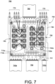
- FIG. 7 is a diagram illustrating an example semiconductor device module (module 700) that is an implementation of the module 300 of FIG. 3 .
- the module 700 includes an encapsulated portion 705, a first column of high-side transistors 710a, a second column of high-side transistors 710b, a first column of low-side transistors 720a, a second column of low-side transistors 720b, a positive power supply terminal 740a, a positive power supply terminal 740b, a negative power supply terminal 750, and an output terminal 760.
- the module 700 further includes signal leads 770, which can be used to communicate signals, such as those described with respect to FIG. 4 .
- the encapsulated portion 705 includes an encapsulation material 780, which can be a molding compound (e.g., an epoxy molding compound, etc.), and a substrate assembly 790 on which a half-bridge circuit is implemented using the columns of high-side transistors and the columns of low-side transistors.
- the encapsulation material 780 can encapsulate the transistors and electrical interconnections (e.g., wire bonds and conductive clips) between the transistors, the substrate, and the signal leads, similar to the encapsulation material 480 of the module 400.
- the encapsulation material 780 is illustrated with transparency to illustrate the structure of the substrate assembly 790 internal to the encapsulation material 780.
- a surface of the substrate of the substrate assembly 790 opposite the surface shown in FIG. 7 can be exposed thorough the encapsulation material 780 to facilitate thermal dissipation for heat generated during electrical operation of the module 700.
- Electrical connections for implementing the half-bridge circuit of FIG. 7 can be made using similar approaches as described above for the module 400 (with respect to FIG. 4 ) and the substrate assembly 490 (with respect to FIG. 5 ). Accordingly, for purposes of brevity, those details are not described again with respect to FIG. 7 .
- the substrate assembly 790 includes a first plurality of a first column of high-side transistors 710a (on a left side of the substrate assembly 790 in the view of FIG. 7 ), and a second column of high-side transistors 710b arranged (adjacent to the first column of high-side transistors 710a with an intervening metal layer portion).
- the substrate assembly 790 also includes a first column of low-side transistors 720a, and a second column of low-side transistors 720b.
- the first column of low-side transistors 720a is adjacent to the second column of high-side transistors 710b (with an intervening metal layer portion), and the first column of low-side transistors 720a is arranged along a right side of the substrate assembly 790, adjacent to the second column of low-side transistors 720b (with an intervening metal layer portion).
- the high-side transistors can be coupled in parallel with each other, and the low-side transistors can be coupled in parallel with each other, such as by using approaches such as those described herein.
- the metal layer portion 740 includes a sub-portion 741 that extends between a part of the metal layer portion 740 on a left side of the ceramic base layer 501 to an attachment pad for the positive power supply terminal 740b.
- the module 700 in the module 700, both columns of the high-side transistors are arranged on the left side of the substrate assembly 790, while both columns of low-side transistors are arranged on the right side of the substrate assembly 790. As a result, this can limit available space for metal layer routing from the positive power supply terminal 740b.
- the sub-portion 741 due to its electrical resistance, can result in portions of the current I p (as described with respect to FIG. 1 ) respectively conducted by the positive power supply terminal 740a and the positive power supply terminal 740b being imbalanced. That is, the portion of the current I p conducted by the positive power supply terminal 740b can be less than the portion of the current I p conducted by the positive power supply terminal 740a.
- the positive power supply terminal 740b can have a narrower width (e.g., the width W4 of the positive power supply terminal 340b of FIG. 3 ) than a width of the positive power supply terminal 740a (e.g., the width W3 of the positive power supply terminal 340a of FIG. 3 ).
- the sub-portion 741 is arranged such that is passes under the output terminal 760. That is, the sub-portion 741 is arranged such that it overlaps, at least in part, with the output terminal 760.
- This arrangement can facilitate current balance between the positive power supply terminal 740a and the positive power supply terminal 740b of the module 700, as well as provide additional magnetic field cancellation (e.g., due to the overlap between the output terminal 760 and the sub-portion 741) to reduce stray inductance.
- a singular form may, unless definitely indicating a particular case in terms of the context, include a plural form.
- Spatially relative terms e.g., over, above, upper, under, beneath, below, lower, top, bottom, and so forth
- the relative terms above and below can, respectively, include vertically above and vertically below.
- the term adjacent can include laterally adjacent to or horizontally adjacent to.
- Some implementations may be implemented using various semiconductor processing and/or packaging techniques. Some implementations may be implemented using various types of semiconductor device processing techniques associated with semiconductor substrates including, but not limited to, for example, silicon (Si), silicon carbide (SiC), gallium arsenide (GaAs), gallium nitride (GaN), and/or so forth.
- semiconductor substrates including, but not limited to, for example, silicon (Si), silicon carbide (SiC), gallium arsenide (GaAs), gallium nitride (GaN), and/or so forth.
Landscapes
- Engineering & Computer Science (AREA)
- Microelectronics & Electronic Packaging (AREA)
- Physics & Mathematics (AREA)
- Electromagnetism (AREA)
- Inverter Devices (AREA)
- Combinations Of Printed Boards (AREA)
- Structure Of Printed Boards (AREA)
Abstract
Description
- This description relates to semiconductor device assemblies. More specifically, this description relates to power semiconductor device modules.
- Semiconductor devices (e.g., semiconductor die) can be included in package assemblies or modules, where such modules can include one or more semiconductor die (e.g., implemented in a circuit included in the module). The performance of semiconductor die, as well as an associated circuit in such modules can be adversely impacted by parasitic impedance, such as parasitic (stray) inductance. For instance, performance of power semiconductor devices in a power module can be affected by stray inductance resulting from magnetic fields associated with high currents conducted by those power semiconductor devices.
- In general aspect, a module can include a substrate having a semiconductor circuit implemented thereon, and a negative power supply terminal electrically coupled with the semiconductor circuit via the substrate. The negative power supply terminal includes a connection tab arranged in a first plane. The module also includes a first positive power supply terminal electrically and a second positive power supply terminal that are coupled with the semiconductor circuit via the substrate. The first positive power supply terminal being laterally disposed from the negative power supply terminal, and including a connection tab arranged in the first plane. The second positive power supply terminal is laterally disposed from the negative power supply terminal and arranged in the first plane, such that the negative power supply terminal is disposed between the first positive power supply terminal and the second positive power supply terminal.
- Implementations can include one or more of the following features, alone or in combination. The first positive power supply terminal and the second positive power supply terminal can be electrically coupled with the semiconductor circuit via a patterned metal layer disposed on a surface of the substrate. The patterned metal layer can include a portion electrically coupling the first positive power supply terminal with the second positive power supply terminal. The surface of the substrate can define a second plane that is parallel to and non-coplanar with the first plane.
- A line orthogonal to the first plane and the second plane can intersect the negative power supply terminal and the portion of the portion of the patterned metal layer electrically coupling the first positive power supply terminal with the second positive power supply terminal.
- The connection tab of the negative power supply terminal, the connection tab of the first positive power supply terminal and the connection tab of the second positive power supply terminal can be disposed external to an encapsulation material of the module along a same edge of the module. The capsulation material can encapsulate the semiconductor circuit and at least a portion of the substrate.
- The semiconductor circuit can be a half-bridge circuit. The negative power supply terminal can be electrically coupled with a low-side switch of the half-bridge circuit, and the first positive power supply terminal and the second positive power supply terminal can be electrically coupled in parallel with each other and electrically coupled with a high-side switch of the half-bridge circuit.
- The low-side switch can include a first plurality of vertical power transistors electrically coupled in parallel with each other. The high-side switch can include a second plurality of vertical power transistors electrically coupled in parallel with each other.
- The module can include an encapsulation material that encapsulates the semiconductor circuit and encapsulates at least a portion of the substrate. The connection tab of the negative power supply terminal, the connection tab of the first positive power supply terminal and the connection tab of the second positive power supply terminal can each extend out of the encapsulation material along respective longitudinal axes that are orthogonal to a same edge of the encapsulation material, the connection tab of the negative power supply terminal can have a first width along a line orthogonal to its respective longitudinal axis. The connection tab of the first positive power supply terminal and the connection tab of the second positive power supply terminal can each have a second width along a line orthogonal to their respective longitudinal axes. The second width can be less than the first width.
- The connection tab of the negative power supply terminal can a first width along a line orthogonal to its respective longitudinal axis, the connection tab of the first positive power supply terminal can have a second width along a line orthogonal to its respective longitudinal axis, the second width being less than the first width. The connection tab of the second positive power supply terminal can have a third width along a line orthogonal to its respective longitudinal axis, the third width being less than the second width.
- The connection tab of the negative power supply terminal, the connection tab of the first positive power supply terminal and the connection tab of the second positive power supply terminal can be disposed along a first edge of the module. The module can include an output terminal electrically coupled with the semiconductor circuit via the substrate. The output terminal can have a connection tab arranged in the first plane. The connection tab of the output terminal can be disposed along a second edge of the module opposite the first edge.
- The semiconductor circuit can be a half-bridge circuit. The output terminal can be electrically coupled with an output node of the half-bridge circuit.
- The substrate can be a direct-bonded-metal substrate.
- The negative power supply terminal can include a first protrusion extending toward the first positive power supply terminal, and a second protrusion extending toward the second positive power supply terminal. The first positive power supply terminal can include a protrusion extending toward the negative power supply terminal that is parallel and coplanar with the first protrusion of the negative power supply terminal. The second positive power supply terminal can include a protrusion extending toward the negative power supply terminal that is parallel and coplanar with the second protrusion of the negative power supply terminal.
- In another general aspect, a module includes a substrate having a half-bridge circuit implemented thereon. The half-bridge circuit includes a plurality of high-side power semiconductor switches electrically coupled in parallel, and a plurality of low-side power semiconductor switches electrically coupled in parallel. The module also includes a negative power supply terminal electrically coupled with the plurality of low-side power semiconductor switches. The negative power supply terminal includes a connection tab arranged in a first plane. The module further includes a first positive power supply terminal and a second positive power supply terminal that are electrically coupled with the plurality of high-side power semiconductor switches. The first positive power supply terminal is laterally disposed from the negative power supply terminal along a first edge of the substrate. The first positive power supply terminal includes a connection tab arranged in the first plane. The second positive power supply terminal is laterally disposed from the negative power supply terminal along the first edge of the substrate. The second positive power supply terminal is arranged in the first plane. The negative power supply terminal being is disposed between the first positive power supply terminal and the second positive power supply terminal.
- Implementations can include one or more of the following features, alone or in combination. For example, the first positive power supply terminal and the second positive power supply terminal can be electrically coupled with the plurality of high-side power semiconductor switches via a patterned metal layer disposed on a surface of the substrate. The patterned metal layer can include a portion electrically coupling the first positive power supply terminal with the second positive power supply terminal. The surface of the substrate can define a second plane that is parallel to and non-coplanar with the first plane. A line orthogonal to the first plane and the second plane can intersects the negative power supply terminal and the portion of the portion of the patterned metal layer electrically coupling the first positive power supply terminal with the second positive power supply terminal.
- The module can include an output terminal electrically coupled with an output node of the half-bridge circuit. The output terminal can include a connection tab arranged in the first plane. The connection tab of the output terminal can be disposed along a second edge of the substrate opposite the first edge.
- The substrate can include a patterned metal layer of the half-bridge circuit. The patterned metal layer can be symmetric along a center line of the substrate extending from the first edge of the substrate to the second edge of the substrate.
- The plurality of high-side power semiconductor switches can include a first column of high-side power semiconductor switches arranged along a third edge of the substrate, and a second column of high-side power semiconductor switches arranged along a fourth edge of the substrate. The third edge of the substrate can be orthogonal to the first edge of the substrate and a second edge of the substrate opposite the first edge of the substrate. The fourth edge of the substrate can be orthogonal to the first edge and the second edge of the substrate. The plurality of low-side power semiconductor switches can be arranged in a first column of low-side power semiconductor switches arranged in parallel with and adjacent to the first column of high-side switches, and a second column of low-side power semiconductor switches arranged in parallel with and disposed between the first column of low-side switches and the second column of high-side switches.
- An arrangement of the first column of high-side power semiconductor switches and the first column of low-side power semiconductor switches can be symmetrical with an arrangement of the second column of high-side power semiconductor switches and the second column of low-side semiconductor switches.
- The plurality of high-side power semiconductor switches can be arranged in a first column of high-side power semiconductor switches arranged along a third edge of the substrate, and a second column of high-side power semiconductor switches arranged in parallel with and adjacent to the first column of high-side power semiconductor switches. The third edge of the substrate can be orthogonal to the first edge of the substrate and a second edge of the substrate opposite the first edge. The plurality of low-side power semiconductor switches can be arranged in a first column of low-side power semiconductor switches arranged along a fourth edge of the substrate, and a second column of low-side power semiconductor switches arranged in parallel with and disposed between the first column of low-side switches and the second column of high-side switches. The fourth edge of the substrate can be orthogonal to the first edge and the second edge of the substrate.
- The negative power supply terminal can include a first protrusion extending toward the first positive power supply terminal, and a second protrusion extending toward the second positive power supply terminal. The first positive power supply terminal can include a protrusion extending toward the negative power supply terminal that is parallel and coplanar with the first protrusion of the negative power supply terminal. The second positive power supply terminal can include a protrusion extending toward the negative power supply terminal that is parallel and coplanar with the second protrusion of the negative power supply terminal.
-
-
FIG. 1 is a schematic diagram illustrating an example power semiconductor circuit that can be included in a semiconductor device module, according to an implementation. -
FIG. 2 is a block diagram illustrating an example semiconductor device module, according to an implementation. -
FIG. 3 is a block diagram illustrating another example semiconductor device module, according to an implementation. -
FIG. 4 is a diagram illustrating an example semiconductor device module that can implement the module ofFIG. 2 . -
FIG. 5 is a diagram illustrating an example substrate assembly that can be included in the module ofFIG. 4 . -
FIG. 6 is a diagram illustrating an isometric view of a cross-section of the module ofFIG. 4 . -
FIG. 7 is a diagram illustrating an example semiconductor device module that can implement the module ofFIG. 3 . - Like reference symbols in the various drawings indicate like elements. Reference numbers for some like elements may not be repeated for all such elements. In certain instances, different reference numbers may be used for like, or similar elements. Some reference numbers for certain elements of a given implementation may not be repeated in each drawing corresponding with that implementation. Some reference numbers for certain elements of a given implementation may be repeated in other drawings corresponding with that implementation, but may not be specifically discussed with reference to each corresponding drawing. The drawings are for purposes of illustrating example implementations and may not necessarily be to scale.
- This disclosure relates to packaged semiconductor device apparatus, which can be referred to as modules, semiconductor device modules, power semiconductor device modules, etc. The approaches illustrated and described herein can be used to implement semiconductor device modules that operate with reduced stray inductance as compared to prior implementations. Such stray inductance can be measured as a series inductance between power supply terminals, e.g., between a DC+ (positive) power supply terminal or terminals and a DC-(negative) power supply terminal or terminals. As indicated above, such stray inductance can be caused (e.g., during operation of a given device) by magnetic fields that are generated by currents flowing into and out of the power supply terminals, where magnetic field lines resulting from current associated with one power supply terminal are incident on a current path associated with another (e.g., coplanar) power supply terminal, and vice versa, result in parasitic (stray) inductance.
- In the approaches described herein, reduced stray inductance (e.g., 15-50 percent reduction as compared to prior approaches) can be achieved as a result of implementing multiple positive power supply terminals (e.g., DC+ terminals) that are each laterally disposed from a negative supply terminal (e.g., a DC- terminal), e.g., laterally spaced on each side of the negative power supply terminal, such that respective current paths for the positive supply terminals and a current path for the negative power supply terminal are coplanar and in parallel with one another. That is, in the disclosed implementations, the current paths can be configured such that a direction of current flow associated with the positive power supply terminals is parallel with, and in an opposite direction of current flow associated with the negative power supply terminal. Such arrangements can reduce stray inductance of a power semiconductor device or module. For instance, such reductions in stray inductance can be realized as a result of mutual interference, or overlap between respective magnetic fields corresponding with currents associated with each of the positive power supply terminals and with a magnetic field corresponding with a current of the negative power supply terminal, causing those magnetic fields to, at least in part, cancel each other, thus reducing stray inductance.
- Also, in example implementations described herein, further reductions in stray inductance can be achieved as result of internal routing, e.g., of metal layers on a substrate, of a semiconductor device module. For instance, routing of a metal layer corresponding with the positive power supply terminals can be arranged such that a portion of that metal layer overlaps with the negative power supply terminal, e.g., to achieve further cancellation of magnetic fields associated with respective currents corresponding with the positive power supply terminals and the negative power supply terminal. For instance, a metal layer corresponding with (electrically coupled with) the positive power supply terminals can include a portion that is, along a line intersecting both the negative power supply terminal and that portion of the metal layer, aligned with a corresponding portion of the negative power supply terminal. That is, in an example frame of reference, a portion of the metal layer associated with the positive power supply terminals can be vertically aligned with a corresponding potion of the negative power supply terminal.
-
FIG. 1 is a schematic diagram illustrating a power semiconductor circuit (circuit 100) that can be included in a semiconductor device module, according to an implementation. In thecircuit 100, a power transistor pair (switch pair, semiconductor switch pair, etc.), which can be referred to as a half-bridge circuit, is shown by way of example and for purposes of illustration. In other implementations, the approaches described herein can be used in conjunction with other semiconductor devices, other power semiconductor circuits, other semiconductor device modules, etc. - As shown in
FIG. 1 , thecircuit 100 can include a first power semiconductor device or switch, atransistor 110, and a second power semiconductor device or switch, atransistor 120. Thetransistor 110 can be referred to as a high-side transistor of the half-bridge circuit, and thetransistor 120 can be referred to as a low-side transistor of the half-bridge circuit. Thetransistor 110 and thetransistor 120 can be implemented in one or more semiconductor die, for instance, thetransistor 110 can be implemented in a first semiconductor die and the transistor and thetransistor 120 can be implemented in a second semiconductor die. In the exampleFIG. 1 , thetransistor 110 and thetransistor 120 are illustrated as insulated-gate bipolar transistors (IGBTs). - In some implementations, other types of power semiconductor devices could be used, such as power metal-oxide semiconductor field effect transistors (power MOSFETs). In some implementations, circuits having other arrangements (and functionality) could be implemented. In some implementations, the
transistor 110 andtransistor 120 can respectively include multiple transistors coupled in parallel with each other. For instance, thetransistor 110 could include two or more power transistors (high-side transistors) coupled in parallel with each other, and thetransistor 120 could include two or more power transistors (low-side transistors) coupled in parallel with each other. - In the
circuit 100, thetransistor 110 includes acollector 112, anemitter 114 and agate 116. Likewise, thetransistor 120 includes acollector 122, anemitter 124 and agate 126. Theemitter 114 of thetransistor 110 and thecollector 122 of thetransistor 120 are electrically coupled to a common node of thecircuit 100, on which an output signal (e.g., an alternating current signal for driving an electric motor of an electric vehicle) can be produced by thecircuit 100. In implementations of thecircuit 100 using power FETs for thetransistor 110 and thetransistor 120, thecollector 112 and thecollector 122 would be drains of respective FETs, and theemitter 114 and theemitter 124 would be sources of the respective FETs. - In the
circuit 100, a positivepower supply terminal 140a (e.g., a DC+ terminal, a Vdd terminal, etc.) and a positivepower supplier terminal 140b can be coupled with thecollector 112 of thetransistor 110. A negative power supply terminal 150 (e.g., a DC- terminal, an electrical ground terminal, etc.) can be coupled with theemitter 124 of thetransistor 120. In some implementations, such as those described herein, the negativepower supply terminal 150 can be disposed between the positivepower supply terminal 140a and the positivepower supplier terminal 140b (e.g., along a same side or edge of a module) to provide for parallel current paths in oppositive directions, such as for a positive supply current IP into thecircuit 100 and a negative power supply current IN out of thecircuit 100, as indicated inFIG. 1 . Further, as described with respect to implementations disclosed herein, routing of a metal layer associated with the positivepower supply terminal 140a and the positivepower supplier terminal 140b can be arranged such that at least a portion of that metal layer overlaps with (e.g., is vertically aligned with) a corresponding portion of the negativepower supply terminal 150. - Further, an
output terminal 160 of thecircuit 100 can be coupled with the common node of theemitter 114 of thetransistor 110 and thecollector 122 of thetransistor 120. As described further below, the positivepower supply terminal 140a, the positivepower supplier terminal 140b, the negativepower supply terminal 150 and theoutput terminal 160 can be implemented using metal terminals (copper terminals, metal leads) that are included in a packaged semiconductor device, each including a connection tab (or plate) that is external to an encapsulation material of an associated module. In some implementations, the positivepower supply terminal 140a, the positivepower supplier terminal 140b, the negativepower supply terminal 150 and theoutput terminal 160 can be electrically and physically coupled with a substrate on which thecircuit 100 is implemented. For instance, the positivepower supply terminal 140a, the positivepower supplier terminal 140b, the negativepower supply terminal 150 and theoutput terminal 160 can be directly bonded (using direct-lead-attachment (DLA)) to the substrate, e.g., via respective leads of the terminals. - As further illustrated in
FIG. 1 , thecircuit 100 can also include a plurality of signal leads that are electrically coupled with respective gate terminals of the transistor110 and thetransistor 120. For instance, as shown inFIG. 1 , asignal lead 170a can be electrically coupled with thegate 116 of thetransistor 110, and asignal lead 170b can be electrically coupled with thegate 126 of thetransistor 120. In other implementations, signal leads, such as thesignal lead 170a and thesignal lead 170b could be electrically (or operatively) coupled with other circuit elements, such as a control circuit (not shown) used to control operation of the half-bridge circuit. The particular signal leads (and connections to/from the signal leads) that are implemented in association with thecircuit 100 will depend on the particular implementation, and the specific configuration of the circuit. As some examples, the signal leads can include gate control signal leads (e.g., as shown inFIG. 1 ), temperature sense signal leads, voltage sense signal leads, etc. -
FIG. 2 is a block diagram illustrating an example semiconductor device module (module 200), according to an implementation. In this example, themodule 200 is an implementation of a half-bridge circuit, such as thecircuit 100 ofFIG. 1 . As shown inFIG. 2 , themodule 200 includes an encapsulatedportion 205, a positivepower supply terminal 240a, a positivepower supply terminal 240b, a negativepower supply terminal 250 and anoutput terminal 260. In some implementations, the encapsulatedportion 205 can include a substate on which a power semiconductor circuit, e.g., the half-bridge circuit, is implemented. The substrate, a plurality of semiconductor die and electrical interconnects, such as wire bonds and conductive clips, of the circuit can be encapsulated in a molding compound, such as an epoxy molding compound. The substrate can be a direct-bonded metal (DBM) substrate, such as a direct-bonded copper (DBC) substrate. In some implementations a surface of the substrate can be exposed through the molding compound, e.g., a surface of the substrate opposite that is opposite a surface on which the half-bridge circuit is disposed. The exposed surface can be used to facilitate dissipation of heat generated during operation of themodule 200, such as for attachment of a thermal dissipation application (e.g., a heat sink, a fluidic cooling jacket, etc.). - In the example implementation of
FIG. 2 , a plurality of transistors for implementing the half-bridge circuit can be implemented in the encapsulatedportion 205, e.g., on the corresponding substrate. For instance, themodule 200 includes a first column of high-side transistors 210a and a second column of high-side transistors 210b. In some implementations, each column of high-side transistors can include a plurality of power transistors, such as vertical IGBTs or vertical MOSFETs. The transistors of the first column of high-side transistors 210a and the transistors of the second column of high-side transistors 210b can coupled in parallel with each other, e.g., via electrical connections on the substrate. That is, the collectors or drains of the high-side transistors can be electrically coupled to a common circuit node that is electrically coupled to the positivepower supply terminal 240a and the positivepower supply terminal 240b. Further, the emitters or sources of the high-side transistors can be electrically coupled to a common circuit node that is electrically coupled to theoutput terminal 260. Similarly, the transistors of the first column of low-side transistors 220a and the transistors of the second column of low-side transistors 220b can coupled in parallel with each other, e.g., via electrical connections on the substrate. That is, the collectors or drains of the low-side transistors can be electrically coupled to a common circuit node that is also electrically coupled to theoutput terminal 260. Further, the emitters or sources of the low-side transistors can be electrically coupled to a common circuit node that is electrically coupled to the negativepower supply terminal 250. - As shown in
FIG. 2 , the positivepower supply terminal 240a, the positivepower supply terminal 240b and the negativepower supply terminal 250 are disposed along a first edge (first side) of themodule 200. In the example ofFIG. 2 , the negativepower supply terminal 250 is disposed between the positivepower supply terminal 240a and the positivepower supply terminal 240b. That is, the positivepower supply terminal 240a can be laterally disposed from the negativepower supply terminal 250 on a first side of the negativepower supply terminal 250, while the positivepower supply terminal 240b is laterally disposed from the negativepower supply terminal 250 on an opposite side of the negativepower supply terminal 250 from the positivepower supply terminal 240a. - In some implementations, respective connection tabs (e.g., for attachment to power rails of system including the module 200) can be arranged in a common plane, e.g., can be coplanar with each other. The connection tabs can be respective portions of the terminals that extend out of the encapsulated
portion 205. This arrangement allows for mutual interference between respective magnetic fields associated with current Ip (e.g., as shown inFIG. 1 ) into themodule 200 conducted by the positivepower supply terminal 240a and the positivepower supply terminal 240b and a magnetic field associated with current In (e.g., as shown inFIG. 1 ) out of themodule 200. Such an arrangement, as a result of magnetic field cancellation due to this mutual interference, can reduce stray inductance of themodule 200 as compared to prior modules with differently arranged power supply terminals (e.g., that do not provide for such cancellation, or have less effective magnetic field cancellation). - In the
module 200, theoutput terminal 260 is disposed on a side (edge) of the encapsulatedportion 205 that is opposite from the edge on which the power supply terminals are located. While not shown inFIG. 2 , themodule 200 can also include one or more signal leads, such as thesignal lead 170a and thesignal lead 170b ofFIG. 1 or other signal leads, such as described herein. - As shown in
FIG. 2 , in this view, the first column of high-side transistors 210a is arranged on a left side of the encapsulated portion 205 (e.g., on an associated substrate), and the second column of high-side transistors 210b is arranged on a right side of the encapsulated portion 205 (e.g., on the associate substrate). The first column of low-side transistors 220a and the second column of low-side transistors 220b are arranged adjacent to one another and between the columns of high-side transistors. Such an arrangement can be achieved, at least in part, using patterned metal on an associated substrate that is symmetrical (e.g., left-to right symmetrical along a center line C-C) for providing electrical interconnections to the high-side and low-side transistors for implementing a half-bridge circuit. Accordingly, an arrangement of the first column of high-side transistors 210a and the first column of low-side transistors 220a can be symmetrical with an arrangement of the second column of high-side transistors 210b and the second column of low-side transistors 220b. Additional electrical interconnects for implementing the circuit (e.g., the circuit 100) can be made using, e.g., wire bonds, conductive clips, etc. This symmetry in arrangement of the columns of the transistors and the associated patterned metal on the substrate can provide for balancing respective portions of the current Ip conducted by the positivepower supply terminal 240a and the positivepower supply terminal 240b. This balanced current distribution can improve performance of the module 200 (e.g., electrical efficiency), as well as increase magnetic field cancellation to reduce stray inductance by also balancing the associated magnetic fields. - In the example of
FIG. 2 , with currents conducted by the positivepower supply terminal 240a and the positivepower supply terminal 240b being balanced, those terminals can be like sized so that current density in each current path into themodule 200 is also balanced. For instance, as shown inFIG. 2 , the positivepower supply terminal 240a and the positivepower supply terminal 240b, as well as the negativepower supply terminal 250 can have a same length L measured from the encapsulatedportion 205 to respective ends of the terminals (e.g., along respective longitudinal axes extending orthogonally from an edge of the encapsulated portion). As also shown inFIG. 2 , the positivepower supply terminal 240a and the positivepower supply terminal 240b can each have a width of W1 (in a direction parallel with the edge of the encapsulated portion 205), while the negativepower supply terminal 250 can have a width of W2, where W2 is greater than W1. In this example, L, W1 and W2 are the dimensions of the portions of the terminals outside the encapsulated portion 205 (e.g., dimensions of the respective connection tabs) and the terminals can extend into the encapsulatedportion 205, such as shown inFIGs. 4 ,6 and7 . The dimensions of L, W1 and W2 will depend on the particular implementation. In an example implementation, L can be on the order of 17 millimeters (mm), W1 can be on the order of 10.4 mm, and W2 can be on the order of 15 mm. The dimensions of theoutput terminal 260 will also depend on the particular implementation. In an example implementation, theoutput terminal 260 can have a length of 13 mm and a width of 14.7. -
FIG. 3 is a block diagram illustrating another example semiconductor device module (module 300), according to an implementation. As with themodule 200 ofFIG. 2 , themodule 300 can implement a half-bridge circuit, such as thecircuit 100 ofFIG. 1 . In this example, themodule 300 includes aspects similar to themodule 200. Accordingly, for purposes of brevity, differences between themodule 300 and themodule 200 are described, and the similar aspects may not be discussed in detail again with respect to themodule 300. - As shown in
FIG. 3 , themodule 300 includes an encapsulatedportion 305, a first column of high-side transistors 310a, a second column of high-side transistors 310b, a first column of low-side transistors 320a, a second column of low-side transistors 320b, a positivepower supply terminal 340a, a positivepower supply terminal 340b, a negativepower supply terminal 350, and anoutput terminal 360. As with themodule 200, themodule 300 can also include one or more signal leads (not shown). - In the
module 300, the first column of high-side transistors 310a and the second column of high-side transistors 310b are disposed adjacent to one another on the left side of a substrate of the encapsulated portion 305 (in the view ofFIG. 3 ), rather than on opposite sides of the substrate as in themodule 200. Also, in themodule 300, the first column of low-side transistors 320a and the second column of low-side transistors 320b are disposed adjacent to one another on the right side of the substrate, rather than between the columns of high-side transistors as in themodule 200. In this arrangement, respective portions of the current Ip conducted by the positivepower supply terminal 340a and the positivepower supply terminal 340b can differ. For instance, more current may conducted by the positivepower supply terminal 340a than the positivepower supply terminal 340b due to the arrangement of the columns of transistors and/or electrical resistance of patterned metal on the associated substrate for conducting these portions of the current Ip. - Accordingly, in order to balance respective current densities in the positive
power supply terminal 340a and the positivepower supply terminal 340b, widths of those terminals can be different. For instance, as shown inFIG. 3 , the positivepower supply terminal 340a has a width of W3 and the positivepower supply terminal 340b has a width of W4, which is less than the width W3. As also shown inFIG. 3 , the negativepower supply terminal 350 has a width of W5 which can be a same width as the width W3, or can be different than the width W3. As with the respective widths of the power supply terminals of themodule 200, the respective widths of the power supply terminals of themodule 300 will depend on the particular implementation. In an example implementation, the width W3 can be on the order of 15 mm, the width W4 can be on the order of 5 mm, and the width W5 can be on the order of 15 mm. This balancing of current densities in the positivepower supply terminal 340a and the positivepower supply terminal 340b can improve electrical performance efficiency of themodule 300, and also improve magnetic field cancellation to reduce stray inductance, as compared to implementations with unbalanced current densities. -
FIG. 4 is a diagram illustrating an example semiconductor device module (module 400) that is an implementation of themodule 200 ofFIG. 2 . As shown inFIG. 4 , themodule 400 includes an encapsulatedportion 405, a first column of high-side transistors 410a, a second column of high-side transistors 410b, a first column of low-side transistors 420a, a second column of low-side transistors 420b, a positivepower supply terminal 440a, a positivepower supply terminal 440b, a negativepower supply terminal 450, and anoutput terminal 460. Themodule 400 further includes a plurality of signal leads (470a-470g). A section line 6-6 is also shownFIG. 4 , which respectively corresponds with the isometric, cross-sectional view ofFIG. 6 . - In this example, the encapsulated
portion 405 includes anencapsulation material 480, which can be a molding compound (e.g., an epoxy molding compound, etc.), and asubstrate assembly 490 on which a half-bridge circuit is implemented using the columns of high-side transistors and columns of low-side transistors. As described herein theencapsulation material 480 can encapsulate the transistors and electrical interconnections (e.g.,wire bonds 495,conductive clips 412, and conductive clips 422) between the transistors, the substrate, and the signal leads. InFIG. 4 , theencapsulation material 480 is illustrated with transparency to illustrate the structure of thesubstrate assembly 490 internal to theencapsulation material 480. As was discussed above, in some implementations, a surface of the substrate opposite the surface shown inFIG. 4 can be exposed thorough theencapsulation material 480 to facilitate thermal dissipation for heat generated during electrical operation of themodule 400. An example implementation of thesubstrate assembly 490 is described in further detail below with reference toFIG. 5 . - As shown in
FIG. 4 , the power supply terminals, and theoutput terminal 460 can be physically and electrically coupled with thesubstrate assembly 490 using DLA, as discussed above. For instance, the positivepower supply terminal 440a can be coupled with the substrate via connection leads 441a, the positivepower supply terminal 440b can be coupled with the substrate via connection leads 441b, and the negativepower supply terminal 450 can be coupled with the substrate via connection leads 451a. The connection leads of the power supply terminals (and connection leads of the output terminal 460) can be monolithically formed with their respective terminal, e.g., by forming bent portions of the terminals using stamping, or other metal-working process. - Also, as shown in
FIG. 4 , one or more signal leads can be physically and electrically coupled to the substrate using DLA, while other signals leads are electrically coupled with the substrate or transistors viawire bonds 495 without being physically coupled to the substrate. As also shown inFIG. 4 , each one of the power supply terminals, theoutput terminal 460 and the signal leads has a portion that is internal to theencapsulation material 480 and a portion that extends outside theencapsulation material 480, e.g., for electrical connection in a corresponding system. As described herein, the portions of the power supply terminals and theoutput terminal 460 disposed outside theencapsulation material 480 can be referred to as connection tabs or tabs. - In the example of
FIG. 4 , the negativepower supply terminal 450 includes aprotrusion 452a (or multiple protrusions) that extends towards the positivepower supply terminal 440a. The negativepower supply terminal 450 also includes aprotrusion 452b (or multiple protrusions) that extends towards the positivepower supply terminal 440b. Further, the positivepower supply terminal 440a includes aprotrusion 442a that extends towards the negativepower supply terminal 450 and overlaps with theprotrusion 452a, and the positivepower supply terminal 440b includes aprotrusion 442b that extends towards the negativepower supply terminal 450 and overlaps with theprotrusion 452b. These overlapping protrusions can provide additional magnetic field cancellation and stray inductance reduction resulting from magnetic fields associated with currents in the power supply terminals. - The signal leads of the
module 400 include asignal lead 470a and asignal lead 470b, which can be used for communicating sense signals for the transistors of the half-bridge circuit. For instance, thesignal lead 470a can be used for a collector or drain sense signal for the high-side transistors, while thesignal lead 470b can be used for an emitter or source sense signal of the high-side transistor. Accordingly, thesignal lead 470a and thesignal lead 470b can be used to determine a current through the parallel connected high-side transistors. The signal leads of themodule 400 also include asignal lead 470c that can be used for a gate control signal for the high-side transistors, asignal lead 470d that can be used for an emitter or source sense signal for the high-side transistors (for determining current in the parallel connected high-side transistors), and asignal lead 470e that can be used for a gate control signal for the high-side transistors. The signal leads of themodule 400 also include asignal lead 470f and asignal lead 470g that can be used for temperature sensing (e.g., to determine an internal operating temperature of the module 400). -
FIG. 5 is a diagram illustrating a substrate assembly that can be included in the module ofFIG. 4 , e.g., thesubstrate assembly 490. Accordingly,FIG. 5 is described with further reference toFIG. 4 . As shown inFIG. 5 , thesubstrate assembly 490 includes asubstrate 500, which can be a DBM substrate, such as a DBC substrate. Thesubstrate 500 can include aceramic base layer 501 and a plurality of metal layer portions that are disposed on theceramic base layer 501. In some implementations, the metal layer portions can be formed (patterned) from a single metal layer, e.g., using a photolithography patterning process, or other process. In some implementations, the metal layer portions can be formed as individual portions, e.g., using one or more deposition processes. The metal layer portions are used for establishing at least some of the electric connections for the half-bridge circuit included on thesubstrate 500. In some implementations, thesubstrate 500 can also include a metal layer on a bottom surface of the ceramic base layer 501 (not visible inFIG. 5 ), where that metal layer facilitates thermal dissipation for the associated module, such as for attachment of a thermal dissipation appliance. - As illustrated in
FIG. 5 , thesubstrate assembly 490 includes a first plurality of high-side transistors 511 arranged in afirst column 510a (on a left side, or along a left edge of theceramic base layer 501 in the view ofFIG. 5 ), and a second plurality of high-side transistors 511 arranged in asecond column 510b (on a right side, or along right edge of the ceramic base layer 501). Collector terminals (for IGBTs) or drain terminals (for MOSFETs) of the high-side transistors 511 can be disposed on ametal layer portion 540. The adjoining (intersecting) edges of thesubstrate 500 can be orthogonal to each other. Themetal layer portion 540 can form a common node that is coupled to a DC+ supply voltage terminal or terminals, e.g., the positivepower supply terminal 440a and the positivepower supply terminal 440b of themodule 400. - In this example, the
substrate assembly 490 also includes a first plurality of low-side transistors 521 arranged in afirst column 520a, and a second plurality of low-side transistors 521 arranged in asecond column 520b. Thefirst column 520a and thesecond column 520b can be adjacent to one another (e.g., with an intervening metal layer portion) and disposed between the columns of high-side transistors (e.g., with respective intervening metal layer portions). Collector terminals (for IGBTs) or drain terminals (for MOSFETs) of the low-side transistors 521 can be disposed on ametal layer portion 560. Themetal layer portion 560 can form a common node that is coupled to an AC output terminal, e.g., theoutput terminal 460 of themodule 400. - As shown in
FIG. 5 ,conductive clips 512 are used for each column of high-side transistors to electrically couple emitter terminals (for IGBTs) or source terminals (for MOSFETs) for the respective high-side transistors 511 of each column together. Theconductive clips 512 are further coupled (electrically and physically) to themetal layer portion 560 to electrically couple the emitter terminals of the high-side transistors 511 of both columns to a common node, e.g., an AC output node. In some implementations, a conductive adhesive, such as solder, can be used to couple theconductive clips 512 with the high-side transistors 511 and themetal layer portion 560. In this example, theconductive clips 512 can be physically coupled with, but electrically insulated from themetal layer portion 540. For instance, an electrically insulative adhesive can be used to physically couple theconductive clips 512 with themetal layer portion 540. - Also, in the
substrate assembly 490 ofFIG. 5 ,conductive clips 522 are used for each column of low-side transistors to electrically couple emitter terminals (for IGBTs) or source terminals (for MOSFETs) for the respective low-side transistors 521 of each column together. Theconductive clips 522 are further coupled with ametal layer portion 550 to electrically couple the emitter terminals or source terminals of the low-side transistors 521 of both columns to a common node, e.g., an DC- supply terminal, such as the negativepower supply terminal 450 of themodule 400. In some implementations, a conductive adhesive, such as solder, can be used to couple theconductive clips 522 with the low-side transistors 521 and themetal layer portion 550. In this example, theconductive clips 522 can be physically coupled with, but electrically insulated from themetal layer portion 560. For instance, an electrically insulative adhesive can be used to physically couple theconductive clips 522 with themetal layer portion 560. - In the
substrate assembly 490,substrate 500 has ametal portion 516a, ametal layer portion 516b, and ametal layer portion 516c disposed on theceramic base layer 501. These metal layer portions can be used, in conjunction with corresponding wires bonds, such as shown inFIG. 4 , for providing a gate control signal (e.g., from thesignal lead 470c of the module 400) to gate terminals of the high-side transistors 511. Thesubstrate 500 of thesubstrate assembly 490 also has ametal portion 526 disposed on theceramic base layer 501. Themetal portion 526 can be used, in conjunction with corresponding wire bonds, such as shown inFIG. 4 , for providing a gate control signal (e.g., from thesignal lead 470e of the module 400) to gate terminals of the low-side transistors 521. In thesubstrate assembly 490, ametal layer portion 570a and ametal layer portion 570b are also disposed on theceramic base layer 501 of thesubstrate 500. As shown inFIG. 4 , themetal layer portion 570a can be used for DLA of thesignal lead 470a, and themetal layer portion 570b can be used for DLA of thesignal lead 470g. Additional electrical interconnections for the half-bridge circuit of thesubstrate assembly 490 shown inFIG. 5 can be made using wire bonds, such as thewire bonds 495 shown inFIG. 4 . - As shown in
FIG. 5 , themetal layer portion 540 includes asub-portion 540a that extends between a part of themetal layer portion 540 on a left side of theceramic base layer 501 to a part of themetal layer portion 540 on a right side of theceramic base layer 501, where themetal layer portion 540, including thesub-portion 540a is electrically continuous. As illustrated inFIG. 5 with further reference toFIG. 4 , thesub-portion 540a is arranged such that is passes under theoutput terminal 460. That is, thesub-portion 540a is arranged such that it overlaps, at least in part, with theoutput terminal 460. This arrangement can facilitate current balance between the positivepower supply terminal 440a and the positivepower supply terminal 440b of themodule 400, as well as provide additional magnetic field cancellation (e.g., due to the overlap between theoutput terminal 460 and the sub-portion 540a) to reduce stray inductance. -
FIG. 6 is a diagram illustrating an isometric view of a cross-section of the module ofFIG. 4 . The cross-section of themodule 400 shownFIG. 6 is along the section line 6-6 inFIG. 4 . Reference numbers for elements ofFIG. 4 andFIG. 5 are included inFIG. 6 for purposes of context, though each of those elements is not described in detail again here with respect toFIG. 6 . Also, in the view ofFIG. 6 , the entireties of the positivepower supply terminal 440a, the negativepower supply terminal 450, theoutput terminal 460, thesignal lead 470a, thesignal lead 470b, and thesignal lead 470c are not shown. Other portions of themodule 400 are not shown inFIG. 4 , as they are removed from the illustrated sectional view. - As can be seen in
FIG. 6 , the negativepower supply terminal 450 is coupled to themetal layer portion 550, e.g., by DLA, via connection leads 451a. As described herein, such connection leads can be formed using a stamping, or other metal working process, by bending a portion of the corresponding terminal, e.g., the negativepower supply terminal 450 to form the connection leads 451a. In this arrangement, a portion of the negativepower supply terminal 450 including a connection tab can be arranged in a first plane, where that first plane is parallel with, but non-coplanar with a second plane in which thesubstrate 500 is arranged, e.g., a plane in which the connection leads 451a are attached to themetal layer portion 550. Accordingly, as is shown inFIG. 1 , the first plane is separated from the second plane, allowing the sub-portion 540a to pass under the negativepower supply terminal 450 to create overlap between the sub-portion 540a and the negativepower supply terminal 450. That is, as shown inFIG. 6 , a vertical line V-V (orthogonal to a plane of the connection tab and orthogonal to a plane of the substrate) that extends through the negativepower supply terminal 450 in the first plane and through the sub-portion 540a in the second plane will intersect both the negativepower supply terminal 450 and thesub-portion 540a. -
FIG. 7 is a diagram illustrating an example semiconductor device module (module 700) that is an implementation of themodule 300 ofFIG. 3 . As shown inFIG. 7 , themodule 700 includes an encapsulatedportion 705, a first column of high-side transistors 710a, a second column of high-side transistors 710b, a first column of low-side transistors 720a, a second column of low-side transistors 720b, a positivepower supply terminal 740a, a positivepower supply terminal 740b, a negativepower supply terminal 750, and anoutput terminal 760. Themodule 700 further includes signal leads 770, which can be used to communicate signals, such as those described with respect toFIG. 4 . - In this example, the encapsulated
portion 705 includes anencapsulation material 780, which can be a molding compound (e.g., an epoxy molding compound, etc.), and asubstrate assembly 790 on which a half-bridge circuit is implemented using the columns of high-side transistors and the columns of low-side transistors. Theencapsulation material 780 can encapsulate the transistors and electrical interconnections (e.g., wire bonds and conductive clips) between the transistors, the substrate, and the signal leads, similar to theencapsulation material 480 of themodule 400. InFIG. 7 , as with theencapsulation material 480, theencapsulation material 780 is illustrated with transparency to illustrate the structure of thesubstrate assembly 790 internal to theencapsulation material 780. In some implementations, a surface of the substrate of thesubstrate assembly 790 opposite the surface shown inFIG. 7 can be exposed thorough theencapsulation material 780 to facilitate thermal dissipation for heat generated during electrical operation of themodule 700. Electrical connections for implementing the half-bridge circuit ofFIG. 7 can be made using similar approaches as described above for the module 400 (with respect toFIG. 4 ) and the substrate assembly 490 (with respect toFIG. 5 ). Accordingly, for purposes of brevity, those details are not described again with respect toFIG. 7 . - As illustrated in
FIG. 7 , thesubstrate assembly 790 includes a first plurality of a first column of high-side transistors 710a (on a left side of thesubstrate assembly 790 in the view ofFIG. 7 ), and a second column of high-side transistors 710b arranged (adjacent to the first column of high-side transistors 710a with an intervening metal layer portion). Thesubstrate assembly 790 also includes a first column of low-side transistors 720a, and a second column of low-side transistors 720b. The first column of low-side transistors 720a is adjacent to the second column of high-side transistors 710b (with an intervening metal layer portion), and the first column of low-side transistors 720a is arranged along a right side of thesubstrate assembly 790, adjacent to the second column of low-side transistors 720b (with an intervening metal layer portion). The high-side transistors can be coupled in parallel with each other, and the low-side transistors can be coupled in parallel with each other, such as by using approaches such as those described herein. - As shown in
FIG. 7 , themetal layer portion 740 includes a sub-portion 741 that extends between a part of themetal layer portion 740 on a left side of theceramic base layer 501 to an attachment pad for the positivepower supply terminal 740b. As compared to themodule 400 and thesubstrate assembly 490, in themodule 700, both columns of the high-side transistors are arranged on the left side of thesubstrate assembly 790, while both columns of low-side transistors are arranged on the right side of thesubstrate assembly 790. As a result, this can limit available space for metal layer routing from the positivepower supply terminal 740b. As a result, in this example arrangement, thesub-portion 741, due to its electrical resistance, can result in portions of the current Ip (as described with respect toFIG. 1 ) respectively conducted by the positivepower supply terminal 740a and the positivepower supply terminal 740b being imbalanced. That is, the portion of the current Ip conducted by the positivepower supply terminal 740b can be less than the portion of the current Ip conducted by the positivepower supply terminal 740a. In order to balance the current densities and corresponding magnetic field between the positivepower supply terminal 740a and the positivepower supply terminal 740b, the positivepower supply terminal 740b can have a narrower width (e.g., the width W4 of the positivepower supply terminal 340b ofFIG. 3 ) than a width of the positivepower supply terminal 740a (e.g., the width W3 of the positivepower supply terminal 340a ofFIG. 3 ). - As illustrated in
FIG. 7 , similar to the sub-portion 540a ofFIG. 5 , thesub-portion 741 is arranged such that is passes under theoutput terminal 760. That is, thesub-portion 741 is arranged such that it overlaps, at least in part, with theoutput terminal 760. This arrangement can facilitate current balance between the positivepower supply terminal 740a and the positivepower supply terminal 740b of themodule 700, as well as provide additional magnetic field cancellation (e.g., due to the overlap between theoutput terminal 760 and the sub-portion 741) to reduce stray inductance. - It will be understood that, in the foregoing description, when an element, such as a layer, a region, or a substrate, is referred to as being on, connected to, electrically connected to, coupled to, or electrically coupled to another element, it may be directly on, connected or coupled to the other element, or one or more intervening elements may be present. In contrast, when an element is referred to as being directly on, directly connected to or directly coupled to another element or layer, there are no intervening elements or layers present. Although the terms directly on, directly connected to, or directly coupled to may not be used throughout the detailed description, elements that are shown as being directly on, directly connected or directly coupled can be referred to as such. The claims of the application may be amended to recite exemplary relationships described in the specification or shown in the figures.
- As used in this specification, a singular form may, unless definitely indicating a particular case in terms of the context, include a plural form. Spatially relative terms (e.g., over, above, upper, under, beneath, below, lower, top, bottom, and so forth) are intended to encompass different orientations of the device in use or operation in addition to the orientation depicted in the figures. In some implementations, the relative terms above and below can, respectively, include vertically above and vertically below. In some implementations, the term adjacent can include laterally adjacent to or horizontally adjacent to.
- Some implementations may be implemented using various semiconductor processing and/or packaging techniques. Some implementations may be implemented using various types of semiconductor device processing techniques associated with semiconductor substrates including, but not limited to, for example, silicon (Si), silicon carbide (SiC), gallium arsenide (GaAs), gallium nitride (GaN), and/or so forth.
- While certain features of the described implementations have been illustrated as described herein, many modifications, substitutions, changes and equivalents will now occur to those skilled in the art. It is, therefore, to be understood that the appended claims are intended to cover all such modifications and changes as fall within the scope of the implementations. It should be understood that they have been presented by way of example only, not limitation, and various changes in form and details may be made. Any portion of the apparatus and/or methods described herein may be combined in any combination, except mutually exclusive combinations. The implementations described herein can include various combinations and/or subcombinations of the functions, components and/or features of the different implementations described.
Claims (15)
- A module comprising:a substrate having a semiconductor circuit implemented thereon;a negative power supply terminal electrically coupled with the semiconductor circuit via the substrate, the negative power supply terminal having a connection tab arranged in a first plane;a first positive power supply terminal electrically coupled with the semiconductor circuit via the substrate, the first positive power supply terminal being laterally disposed from the negative power supply terminal, the first positive power supply terminal having a connection tab arranged in the first plane; anda second positive power supply terminal electrically coupled with the semiconductor circuit via the substrate, the second positive power supply terminal being laterally disposed from the negative power supply terminal, the second positive power supply terminal being arranged in the first plane, the negative power supply terminal being disposed between the first positive power supply terminal and the second positive power supply terminal.
- The module of claim 1, wherein the first positive power supply terminal and the second positive power supply terminal are electrically coupled with the semiconductor circuit via a patterned metal layer disposed on a surface of the substrate, the patterned metal layer including a portion electrically coupling the first positive power supply terminal with the second positive power supply terminal, the surface of the substrate defining a second plane that is parallel to and non-coplanar with the first plane.
- The module of claim 2, wherein a line orthogonal to the first plane and the second plane intersects the negative power supply terminal and the portion of the portion of the patterned metal layer electrically coupling the first positive power supply terminal with the second positive power supply terminal.
- The module of claim 1, wherein the connection tab of the negative power supply terminal, the connection tab of the first positive power supply terminal and the connection tab of the second positive power supply terminal are disposed external to an encapsulation material of the module along a same edge of the module, the encapsulation material encapsulating the semiconductor circuit and at least a portion of the substrate.
- The module of claim 1, wherein:the semiconductor circuit is a half-bridge circuit;the negative power supply terminal is electrically coupled with a low-side switch of the half-bridge circuit; andthe first positive power supply terminal and the second positive power supply terminal are electrically coupled in parallel with each other and electrically coupled with a high-side switch of the half-bridge circuit.
- The module of claim 5, wherein the substrate includes a patterned metal layer of the half-bridge circuit, the patterned metal layer being symmetric along a center line of the substrate extending from a first edge of the substrate to a second edge of the substrate, opposite the first edge.
- The module of claim 5, wherein:the low-side switch includes a first plurality of power transistors electrically coupled in parallel with each other; andthe high-side switch includes a second plurality of power transistors electrically coupled in parallel with each other.
- The module of claim 7, wherein:the first plurality of power transistors are arranged in:a first column of high-side power transistors arranged along a first edge of the substrate; anda second column of high-side power transistors arranged along a second edge of the substrate, opposite the first edge of the substrate; andthe second plurality of power transistors are arranged in:a first column of low-side power transistors arranged in parallel with and adjacent to the first column of high-side power transistors; anda second column of low-side power transistors arranged in parallel with and disposed between the first column of low-side power transistors and the second column of high-side power transistors; andan arrangement of the first column of high-side power transistors and the first column of low-side power transistors is symmetrical with an arrangement of the second column of high-side power transistors and the second column of low-side power transistors.
- The module of claim 7, wherein:the first plurality of power transistors are arranged in:a first column of high-side power transistors arranged along a first edge of the substrate; anda second column of high-side power transistors arranged in parallel with and adjacent to the first column of high-side power transistors; andthe second plurality of power transistors are arranged in:a first column of low-side power transistors arranged along a second edge of the substrate, opposite the first edge of the substrate; anda second column of low-side power transistors arranged in parallel with and disposed between the first column of low-side power transistors and the second column of high-side power transistors.
- The module of claim 1, further comprising:an encapsulation material that encapsulates the semiconductor circuit and encapsulates at least a portion of the substrate,the connection tab of the negative power supply terminal, the connection tab of the first positive power supply terminal and the connection tab of the second positive power supply terminal each extending out of the encapsulation material along respective longitudinal axes that are orthogonal to a same edge of the encapsulation material,the connection tab of the negative power supply terminal having a first width along a line orthogonal to its respective longitudinal axis; andthe connection tab of the first positive power supply terminal and the connection tab of the second positive power supply terminal each having a second width along a line orthogonal to their respective longitudinal axes, the second width being less than the first width.
- The module of claim 1, further comprising:an encapsulation material that encapsulates the semiconductor circuit and encapsulates at least a portion of the substrate,the connection tab of the negative power supply terminal, the connection tab of the first positive power supply terminal and the connection tab of the second positive power supply terminal each extending out of the encapsulation material along respective longitudinal axes that are orthogonal to a same edge of the encapsulation material,the connection tab of the negative power supply terminal having a first width along a line orthogonal to its respective longitudinal axis;the connection tab of the first positive power supply terminal having a second width along a line orthogonal to its respective longitudinal axis, the second width being less than the first width; andthe connection tab of the second positive power supply terminal having a third width along a line orthogonal to its respective longitudinal axis, the third width being less than the second width.
- The module of claim 1, wherein the connection tab of the negative power supply terminal, the connection tab of the first positive power supply terminal and the connection tab of the second positive power supply terminal are disposed along a first edge of the module,
the module further comprising an output terminal electrically coupled with the semiconductor circuit via the substrate, the output terminal having a connection tab arranged in the first plane, the connection tab of the output terminal being disposed along a second edge of the module opposite the first edge. - The module of claim 12, wherein:the semiconductor circuit is a half-bridge circuit; andthe output terminal is electrically coupled with an output node of the half-bridge circuit.
- The module of claim 1, wherein the substrate is a direct-bonded-metal substrate.
- The module of claim 1, wherein:the negative power supply terminal includes:a first protrusion extending toward the first positive power supply terminal;a second protrusion extending toward the second positive power supply terminal;the first positive power supply terminal includes a protrusion extending toward the negative power supply terminal that is parallel and coplanar with the first protrusion of the negative power supply terminal; andthe second positive power supply terminal includes a protrusion extending toward the negative power supply terminal that is parallel and coplanar with the second protrusion of the negative power supply terminal.
Applications Claiming Priority (1)
| Application Number | Priority Date | Filing Date | Title |
|---|---|---|---|
| US202263299147P | 2022-01-13 | 2022-01-13 |
Publications (2)
| Publication Number | Publication Date |
|---|---|
| EP4224523A2 true EP4224523A2 (en) | 2023-08-09 |
| EP4224523A3 EP4224523A3 (en) | 2023-12-20 |
Family
ID=84981218
Family Applications (1)
| Application Number | Title | Priority Date | Filing Date |
|---|---|---|---|
| EP23151438.1A Pending EP4224523A3 (en) | 2022-01-13 | 2023-01-13 | Stray inductance reduction in power semiconductor device modules |
Country Status (4)
| Country | Link |
|---|---|
| US (2) | US12471204B2 (en) |
| EP (1) | EP4224523A3 (en) |
| KR (1) | KR20230109589A (en) |
| CN (1) | CN116435278A (en) |
Families Citing this family (7)
| Publication number | Priority date | Publication date | Assignee | Title |
|---|---|---|---|---|
| US12451817B2 (en) * | 2022-06-02 | 2025-10-21 | Sentec E&E Co., Ltd. | Power module |
| CN118198020A (en) * | 2022-12-13 | 2024-06-14 | 台达电子工业股份有限公司 | Power Module |
| CN117276226B (en) * | 2023-11-01 | 2024-04-16 | 深圳基本半导体有限公司 | Power module, packaging structure and electronic equipment |
| CN117476581A (en) * | 2023-12-27 | 2024-01-30 | 深圳平创半导体有限公司 | Power semiconductor device based on general assembly structure |
| US20250392229A1 (en) * | 2024-06-21 | 2025-12-25 | BorgWarner US Technologies LLC | Double-side cooled triple-dc-port half-bridge power module |
| CN119335349B (en) * | 2024-12-17 | 2025-03-18 | 赛英特半导体技术(西安)有限公司 | A dynamic parameter test circuit and test method for wafer |
| CN121604850A (en) * | 2026-01-29 | 2026-03-03 | 北一半导体科技(广东)有限公司 | SiC power module with embedded shell and assembling method |
Family Cites Families (32)
| Publication number | Priority date | Publication date | Assignee | Title |
|---|---|---|---|---|
| JP2001326325A (en) | 2000-05-16 | 2001-11-22 | Seiko Epson Corp | Semiconductor device and manufacturing method thereof |
| CN201011655Y (en) | 2007-01-10 | 2008-01-23 | 上海凯虹科技电子有限公司 | A frame of a high-power semiconductor device |
| JP4567029B2 (en) | 2007-06-22 | 2010-10-20 | 日立オートモティブシステムズ株式会社 | Power converter |
| JP4958735B2 (en) | 2007-11-01 | 2012-06-20 | 株式会社日立製作所 | Power semiconductor module manufacturing method, power semiconductor module manufacturing apparatus, power semiconductor module, and joining method |
| US8018054B2 (en) | 2008-03-12 | 2011-09-13 | Fairchild Semiconductor Corporation | Semiconductor die package including multiple semiconductor dice |
| JP5407198B2 (en) | 2008-07-02 | 2014-02-05 | 富士電機株式会社 | Power module for power converter |
| US7759778B2 (en) | 2008-09-15 | 2010-07-20 | Delphi Technologies, Inc. | Leaded semiconductor power module with direct bonding and double sided cooling |
| JP5557441B2 (en) | 2008-10-31 | 2014-07-23 | 日立オートモティブシステムズ株式会社 | Power converter and electric vehicle |
| JP5253430B2 (en) | 2009-03-23 | 2013-07-31 | 株式会社豊田中央研究所 | Power module |
| JP5557585B2 (en) | 2010-04-26 | 2014-07-23 | 日立オートモティブシステムズ株式会社 | Power module |
| US9184117B2 (en) | 2010-06-18 | 2015-11-10 | Alpha And Omega Semiconductor Incorporated | Stacked dual-chip packaging structure and preparation method thereof |
| JP5520889B2 (en) | 2011-06-24 | 2014-06-11 | 日立オートモティブシステムズ株式会社 | Power semiconductor module and power converter using the same |
| KR101388857B1 (en) | 2012-06-29 | 2014-04-23 | 삼성전기주식회사 | Semiconductor package and method of manufacturing the semiconductor package |
| US8441128B2 (en) | 2011-08-16 | 2013-05-14 | Infineon Technologies Ag | Semiconductor arrangement |
| DE112013003222B4 (en) | 2012-06-29 | 2021-08-19 | Denso Corporation | Semiconductor device and semiconductor device connection structure |
| US8921989B2 (en) | 2013-03-27 | 2014-12-30 | Toyota Motor Engineering & Manufacturing North, America, Inc. | Power electronics modules with solder layers having reduced thermal stress |
| US9214415B2 (en) | 2013-04-11 | 2015-12-15 | Texas Instruments Incorporated | Integrating multi-output power converters having vertically stacked semiconductor chips |
| CN105247675B (en) | 2013-05-29 | 2019-11-15 | 三菱电机株式会社 | Semiconductor device with a plurality of semiconductor chips |
| JP6215151B2 (en) | 2014-08-01 | 2017-10-18 | 日立オートモティブシステムズ株式会社 | Power converter |
| JP6376917B2 (en) | 2014-09-18 | 2018-08-22 | 日立オートモティブシステムズ株式会社 | Electronic control device and electric power steering device |
| EP3246945B1 (en) * | 2016-05-19 | 2018-10-03 | ABB Schweiz AG | Power module with low stray inductance |
| DE102016120778B4 (en) | 2016-10-31 | 2024-01-25 | Infineon Technologies Ag | Assembly with vertically spaced, partially encapsulated contact structures |
| KR101956997B1 (en) * | 2016-12-15 | 2019-03-12 | 현대자동차주식회사 | Hybrid-type power module of double side cooling |
| US10917992B2 (en) * | 2017-01-13 | 2021-02-09 | Cree Fayetteville, Inc. | High power multilayer module having low inductance and fast switching for paralleling power devices |
| US10090279B2 (en) | 2017-03-03 | 2018-10-02 | Semiconductor Components Industries, Llc | Stray inductance reduction in packaged semiconductor devices and modules |
| JP6717270B2 (en) * | 2017-07-27 | 2020-07-01 | 株式会社デンソー | Semiconductor module |
| US11107761B2 (en) | 2018-02-06 | 2021-08-31 | Denso Corporation | Semiconductor device |
| DE102019112935B4 (en) * | 2019-05-16 | 2021-04-29 | Danfoss Silicon Power Gmbh | Semiconductor module |
| US11031379B2 (en) | 2019-09-04 | 2021-06-08 | Semiconductor Components Industries, Llc | Stray inductance reduction in packaged semiconductor devices |
| JP6906583B2 (en) * | 2019-10-29 | 2021-07-21 | 三菱電機株式会社 | Semiconductor power module |
| WO2021130290A1 (en) * | 2019-12-28 | 2021-07-01 | Danfoss Silicon Power Gmbh | Power module with improved electrical characteristics |
| US12476397B2 (en) * | 2022-04-07 | 2025-11-18 | Semiconductor Components Industries, Llc | Transfer molded power modules and methods of manufacture |
-
2023
- 2023-01-13 KR KR1020230005703A patent/KR20230109589A/en active Pending
- 2023-01-13 EP EP23151438.1A patent/EP4224523A3/en active Pending
- 2023-01-13 CN CN202310071611.4A patent/CN116435278A/en active Pending
- 2023-01-13 US US18/154,303 patent/US12471204B2/en active Active
-
2025
- 2025-11-10 US US19/384,382 patent/US20260068033A1/en active Pending
Also Published As
| Publication number | Publication date |
|---|---|
| KR20230109589A (en) | 2023-07-20 |
| CN116435278A (en) | 2023-07-14 |
| US12471204B2 (en) | 2025-11-11 |
| EP4224523A3 (en) | 2023-12-20 |
| US20260068033A1 (en) | 2026-03-05 |
| US20230225044A1 (en) | 2023-07-13 |
Similar Documents
| Publication | Publication Date | Title |
|---|---|---|
| US12471204B2 (en) | Semiconductor device modules | |
| US11270984B2 (en) | Semiconductor module | |
| US20250379124A1 (en) | Power circuit module | |
| US6845017B2 (en) | Substrate-level DC bus design to reduce module inductance | |
| US11456238B2 (en) | Semiconductor device including a semiconductor chip connected with a plurality of main terminals | |
| US11031379B2 (en) | Stray inductance reduction in packaged semiconductor devices | |
| EP3522213B1 (en) | Semiconductor device | |
| US20200035616A1 (en) | Semiconductor Package Having an Electromagnetic Shielding Structure and Method for Producing the Same | |
| US8466549B2 (en) | Semiconductor device for power conversion | |
| US20230253304A1 (en) | Semiconductor module having a multi-branch switch node connector | |
| US11996344B2 (en) | Semiconductor device | |
| CN117276226A (en) | Power modules, packaging structures and electronic equipment | |
| JP7484156B2 (en) | Semiconductor Device | |
| US12550263B2 (en) | Switching oscillation reduction for power semiconductor device modules | |
| US12550754B2 (en) | Current sharing mismatch reduction in power semiconductor device modules | |
| US20240162197A1 (en) | Scalable power semiconductor device package with low inductance | |
| WO2024132151A1 (en) | Power semiconductor module | |
| JP3525823B2 (en) | Mounting structure of complementary IGBT | |
| TWI905935B (en) | Semiconductor Module | |
| TWI895998B (en) | semiconductor modules | |
| CN117476585A (en) | Semiconductor module | |
| WO2024143541A1 (en) | Semiconductor device, semiconductor module, and manufacturing method | |
| CN115411008A (en) | Switching device, semiconductor device, and method for manufacturing switching device |
Legal Events
| Date | Code | Title | Description |
|---|---|---|---|
| PUAI | Public reference made under article 153(3) epc to a published international application that has entered the european phase |
Free format text: ORIGINAL CODE: 0009012 |
|
| STAA | Information on the status of an ep patent application or granted ep patent |
Free format text: STATUS: THE APPLICATION HAS BEEN PUBLISHED |
|
| AK | Designated contracting states |
Kind code of ref document: A2 Designated state(s): AL AT BE BG CH CY CZ DE DK EE ES FI FR GB GR HR HU IE IS IT LI LT LU LV MC ME MK MT NL NO PL PT RO RS SE SI SK SM TR |
|
| PUAL | Search report despatched |
Free format text: ORIGINAL CODE: 0009013 |
|
| AK | Designated contracting states |
Kind code of ref document: A3 Designated state(s): AL AT BE BG CH CY CZ DE DK EE ES FI FR GB GR HR HU IE IS IT LI LT LU LV MC ME MK MT NL NO PL PT RO RS SE SI SK SM TR |
|
| RIC1 | Information provided on ipc code assigned before grant |
Ipc: H01L 23/00 20060101ALN20231116BHEP Ipc: H01L 23/373 20060101ALN20231116BHEP Ipc: H01L 23/31 20060101ALN20231116BHEP Ipc: H01L 25/07 20060101AFI20231116BHEP |
|
| STAA | Information on the status of an ep patent application or granted ep patent |
Free format text: STATUS: REQUEST FOR EXAMINATION WAS MADE |
|
| 17P | Request for examination filed |
Effective date: 20240620 |
|
| RBV | Designated contracting states (corrected) |
Designated state(s): AL AT BE BG CH CY CZ DE DK EE ES FI FR GB GR HR HU IE IS IT LI LT LU LV MC ME MK MT NL NO PL PT RO RS SE SI SK SM TR |
|
| RAP3 | Party data changed (applicant data changed or rights of an application transferred) |
Owner name: SEMICONDUCTOR COMPONENTS INDUSTRIES, LLC |