EP4220972A1 - Antenna device and electronic circuit protective device - Google Patents
Antenna device and electronic circuit protective device Download PDFInfo
- Publication number
- EP4220972A1 EP4220972A1 EP21872248.6A EP21872248A EP4220972A1 EP 4220972 A1 EP4220972 A1 EP 4220972A1 EP 21872248 A EP21872248 A EP 21872248A EP 4220972 A1 EP4220972 A1 EP 4220972A1
- Authority
- EP
- European Patent Office
- Prior art keywords
- antenna
- reactance
- electronic circuit
- antenna device
- adjustment device
- Prior art date
- Legal status (The legal status is an assumption and is not a legal conclusion. Google has not performed a legal analysis and makes no representation as to the accuracy of the status listed.)
- Pending
Links
Images







Classifications
-
- H—ELECTRICITY
- H01—ELECTRIC ELEMENTS
- H01Q—ANTENNAS, i.e. RADIO AERIALS
- H01Q23/00—Antennas with active circuits or circuit elements integrated within them or attached to them
-
- H—ELECTRICITY
- H01—ELECTRIC ELEMENTS
- H01Q—ANTENNAS, i.e. RADIO AERIALS
- H01Q1/00—Details of, or arrangements associated with, antennas
- H01Q1/27—Adaptation for use in or on movable bodies
- H01Q1/32—Adaptation for use in or on road or rail vehicles
- H01Q1/325—Adaptation for use in or on road or rail vehicles characterised by the location of the antenna on the vehicle
- H01Q1/3275—Adaptation for use in or on road or rail vehicles characterised by the location of the antenna on the vehicle mounted on a horizontal surface of the vehicle, e.g. on roof, hood, trunk
-
- H—ELECTRICITY
- H01—ELECTRIC ELEMENTS
- H01Q—ANTENNAS, i.e. RADIO AERIALS
- H01Q1/00—Details of, or arrangements associated with, antennas
- H01Q1/12—Supports; Mounting means
-
- H—ELECTRICITY
- H01—ELECTRIC ELEMENTS
- H01Q—ANTENNAS, i.e. RADIO AERIALS
- H01Q1/00—Details of, or arrangements associated with, antennas
- H01Q1/50—Structural association of antennas with earthing switches, lead-in devices or lightning protectors
-
- H—ELECTRICITY
- H01—ELECTRIC ELEMENTS
- H01Q—ANTENNAS, i.e. RADIO AERIALS
- H01Q1/00—Details of, or arrangements associated with, antennas
- H01Q1/52—Means for reducing coupling between antennas; Means for reducing coupling between an antenna and another structure
- H01Q1/521—Means for reducing coupling between antennas; Means for reducing coupling between an antenna and another structure reducing the coupling between adjacent antennas
-
- H—ELECTRICITY
- H01—ELECTRIC ELEMENTS
- H01Q—ANTENNAS, i.e. RADIO AERIALS
- H01Q5/00—Arrangements for simultaneous operation of antennas on two or more different wavebands, e.g. dual-band or multi-band arrangements
- H01Q5/30—Arrangements for providing operation on different wavebands
- H01Q5/307—Individual or coupled radiating elements, each element being fed in an unspecified way
- H01Q5/314—Individual or coupled radiating elements, each element being fed in an unspecified way using frequency dependent circuits or components, e.g. trap circuits or capacitors
- H01Q5/335—Individual or coupled radiating elements, each element being fed in an unspecified way using frequency dependent circuits or components, e.g. trap circuits or capacitors at the feed, e.g. for impedance matching
-
- H—ELECTRICITY
- H01—ELECTRIC ELEMENTS
- H01Q—ANTENNAS, i.e. RADIO AERIALS
- H01Q5/00—Arrangements for simultaneous operation of antennas on two or more different wavebands, e.g. dual-band or multi-band arrangements
- H01Q5/50—Feeding or matching arrangements for broad-band or multi-band operation
-
- H—ELECTRICITY
- H01—ELECTRIC ELEMENTS
- H01Q—ANTENNAS, i.e. RADIO AERIALS
- H01Q9/00—Electrically-short antennas having dimensions not more than twice the operating wavelength and consisting of conductive active radiating elements
- H01Q9/04—Resonant antennas
- H01Q9/30—Resonant antennas with feed to end of elongated active element, e.g. unipole
- H01Q9/32—Vertical arrangement of element
- H01Q9/36—Vertical arrangement of element with top loading
-
- H—ELECTRICITY
- H04—ELECTRIC COMMUNICATION TECHNIQUE
- H04B—TRANSMISSION
- H04B1/00—Details of transmission systems, not covered by a single one of groups H04B3/00 - H04B13/00; Details of transmission systems not characterised by the medium used for transmission
- H04B1/06—Receivers
- H04B1/16—Circuits
- H04B1/18—Input circuits, e.g. for coupling to an antenna or a transmission line
Definitions
- the present invention relates to an antenna device that is mountable on a moving body or the like and an electronic circuit protection device.
- Patent Literature 1 discloses an antenna device for a vehicle having two antenna elements corresponding to two types of frequency bands, and an attenuation circuit that attenuates a signal of the other frequency band is connected to one of the two antenna elements.
- Patent Literature 2 discloses an antenna device mounted with a protection circuit between an antenna part and an electronic circuit (external connection terminal), one end of the protection circuit being grounded, the other end being connected to a line connecting the antenna part and the electronic circuit.
- the protection circuit causes a surge current caused by a surge voltage that instantaneously exceeds a steady state to flow to a ground side.
- the attenuation circuit and the protection circuit as above normally function as protection devices for eliminating electrical stresses in electronic circuits that are used in environments where the electronic circuits can receive the electrical stresses caused by occurrences of an unintentional electromagnetic field, voltage, and current.
- Patent Literatures 1 and 2 can be said to be very useful devices for electronic circuits that must be used in environments that can receive electrical stresses.
- One example of objects of the present disclosure is to make it possible, in an antenna device, to protect components of an electronic circuit used in an environment that can receive electrical stress from such electrical stress, and to relieve an influence on signal transmission.
- the other objects of the present disclosure will become apparent from the description herein.
- One aspect of the present disclosure is an antenna device including an antenna part, a board to which the antenna part is connected, an electronic circuit mounted to the board, and a reactance adjustment device that cancels reactance in a frequency band in use, the reactance causing electrical stress to be applied to a component of the electronic circuit, wherein the board includes a board input part serving as an input interface with the antenna part, and the reactance adjustment device is mounted between the board input part and the electronic circuit, and is connected to a ground part.
- an antenna device including an antenna part, a board to which the antenna part is connected, an electronic circuit mounted to the board, and a reactance adjustment device that cancels reactance in a frequency band in use, the reactance causing electrical stress to be applied to a component of the electronic circuit, wherein the board includes an external connection part to be connected to external electronic equipment, and the reactance adjustment device is mounted between the electronic circuit and the external connection part, and is connected to a ground part.
- an electronic circuit protection device including an electronic circuit, an additional device that is connected between an input side or an output side of the electronic circuit, and a ground part, and is added to protect a component of the electronic circuit from electrical stress, and a reactance adjustment device that cancels reactance of the additional device in a frequency band in use.
- the antenna device receives signals from 470 MHz to 720 MHz that are in a DTTB (Digital Television Terrestrial Broadcasting System) band.
- DTTB Digital Television Terrestrial Broadcasting System
- An antenna device 10 shown in Figure 1 is configured by accommodating an antenna part 11 and a circuit board 12 in an antenna case described later and attached to a vehicle roof or the like.
- the antenna part 11 is configured by a planar conductor, a linear (including rod-shaped) conductor or a conductor in which these conductors are combined, which resonates in the DTTB band.
- electronic components including active elements such as transistors and diodes are implemented.
- the board input part A and the circuit input part B are electrically connected with a line 13 such as a conductor pattern.
- What is arranged between the board input part A and the circuit input part B is not limited to a conductor pattern.
- One or a plurality of circuits may be arranged between the board input part A and the circuit input part B, for example, either one or both of an additional device 15 described later and a reactance pattern 211 may be arranged.
- a characteristic impedance at a time of an antenna part 11 side being seen from the board input part A is 50 ⁇ in the present example
- an impedance at a time of an electronic circuit 14 side being seen from the circuit input part B is also 50 ⁇ in the present example.
- an impedance of the line 13 between the board input part A and the circuit input part B is also 50 ⁇
- the impedances in a system to the electronic circuit 14 from the antenna part 11 are matched and a transmission loss of power (signal level) at a time of signal transmission hardly occurs.
- the electronic circuit 14 is configured by including the plurality of electronic components described above, and these electronic components include many electronic components that are vulnerable to the aforementioned electrical stress. Therefore, in a case where antenna parts for other frequency bands, electronic circuits, and the like are closely arranged in the antenna case, a strong transmission wave is outputted from an antenna device mounted to another vehicle traveling in a vicinity, or a surge exceeding a steady state instantaneously occurs, the electronic circuit 14 is severely influenced, even if it is an electromagnetic wave or voltage at a frequency different from the DTTB band. Therefore, in the first embodiment, the additional device 15 for eliminating electrical stress is mounted in a front stage of the electronic circuit 14 as in an antenna device 20 shown in Figure 2 .
- the additional device 15 is a semiconductor diode with two terminals in the present example, one end thereof is connected to the line 13, and the other end is connected to a ground part.
- the additional device 15 has capacitance (capacitive reactance) that is inter-terminal capacitance.
- the inter-terminal capacitance is about 0.2 pF to 30 pF depending on a type of the semiconductor diode, and is 7 pF in the DTTB band in the case of the present example.
- the impedance at the time of the electronic circuit 14 side being seen from the board input part A becomes capacitive in the DTTB band, and transmission loss of power that is transmitted from the board input part A to the circuit input part B increases. Therefore, an antenna gain is reduced.
- a reactance adjustment device 16 that cancels a fluctuation in reactance caused by the presence of the additional device 15 is mounted in parallel with the additional device 15 while making use of the electrical stress elimination operation by the additional device 15.
- the reactance adjustment device 16 is an inductive reactance element having inductance of 10.2 nH in the DTTB band in the present example, one end thereof is connected to the line 13, and the other end is connected to a ground part.
- a type and a mode of the inductive reactance element may be arbitrary, but by using a chip inductor, the inductive reactance element becomes compacter (thinner) than a coil, and has an advantage that even when it is implemented in the circuit board 12 with the additional device 15, a design size of the circuit board 12 does not have to be changed.
- the inductive reactance element may be configured by a combination of a plurality of conductor patterns instead of the chip inductor.
- Inductance of the reactance adjustment device 16 is desirably set so that a reactance component of the inductance is in a complex conjugate relationship to the inter-terminal capacitance of the additional device 15.
- Complex conjugate means that the polarities are opposite and the magnitudes are equal.
- the "complex conjugate relationship” means a relationship in which when reactance of the additional device 15 is jX, reactance of the reactance adjustment device 16 is +jX.
- capacitive reactance of the additional device 15 in the DTTB band is cancelled by inductive reactance of the reactance adjustment device 16, and impedance between the board input part A and the circuit input part B becomes 50 ⁇ .
- the capacitive reactance of the additional device 15 is approximately -j24.1 ( ⁇ ) in the frequency of 595 MHz
- the inductive reactance of the reactance adjustment device 16 is +j24.1 ( ⁇ )
- the impedances are in a complex conjugate relationship.
- the reactance adjustment device 16 is arranged at a position as close as possible to an arrangement position of the additional device 15. Thereby, it is possible to suppress inductance and capacitance of the line 13 from the additional device 15 to the reactance adjustment device 16.
- the reactance adjustment device 16 is arranged in a range within 1/10 wavelength of the highest frequency in the DTTB band from the position in which the additional device 15 is arranged. Thereby, it is possible to further reduce the influence of inductance and capacitance of the line 13.
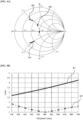
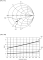
- Figure 4A is a Smith chart showing the loci of impedances in the reactance adjustment device 16 alone, and the antenna device 20 and the antenna device 30.
- an upper half region of the Smith chart shows inductivity, and a lower half region shows capacitance.
- a solid line 401 shows a locus of impedance in the antenna device 20
- an alternate long and short dash line 402 shows a locus of the impedance in the antenna device 30
- a dotted line 403 shows a locus of the impedance in the reactance adjustment device 16 alone.
- the locus 403 of the impedance in the reactance adjustment device 16 alone is inductive throughout an entire region of the DTTB band as a matter of course.
- the locus 401 of the impedance of the antenna device 20 is capacitive throughout the entire region of the DTTB band. Further, the locus 401 of the impedance is substantially symmetrical about a horizontal axis with the locus 403 of the impedance in the reactance adjustment device 16 alone, and is in the lower half region of the Smith chart.
- the locus 402 of the impedance in the antenna device 30 passes through the horizontal axis in a vicinity of 1.0 of the Smith chart center.
- the antenna device 30 having the reactance adjustment device 16 having a complex conjugate relationship to the inter-terminal capacitance of the additional device 15 reduces the transmission loss caused by the presence of the additional device 15.
- Figure 4B is a VSWR characteristic diagram in the antenna device 20 and the antenna device 30.
- an axis of ordinates represents VSWR
- an axis of abscissas represents a frequency (MHz).
- a solid line 411 represents a VSWR characteristic in the antenna device 20
- an alternate long and short dash line 412 represents a VSWR characteristic in the antenna device 30.
- the VSWR in the antenna device 20 becomes larger substantially rectilinearly as the frequency becomes higher, and the minimum value thereof is 2.7, whereas a maximum value is 4.3.
- the alternate long and short dash line 412 in Figure 4B the VSWR of the antenna device 30 reaches a minimum value 1.0 in a vicinity of a frequency 600 MHz, and a maximum value thereof is 1.9.
- VSWR is less than 2 in all frequencies in the DTTB band.
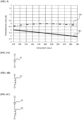
- FIG. 5 is a graph representing transmission loss characteristics in the antenna device 20 and the antenna device 30.
- a transmission loss in the antenna device 10 shown in Figure 1 is set as 0 dB.
- a solid line 501 represents a transmission loss (dB) by the configuration of the antenna device 20.
- the transmission loss is larger than -1 dB throughout an entire region of the DTTB band.
- An alternate long and short dash line 502 represents a transmission loss (dB) of the antenna device 30.
- the transmission loss in the antenna device 30 is substantially 0 dB throughout a substantially entire region of the DTTB band, a fluctuation by the frequency is also small, and the transmission loss is about -0.4 dB at a maximum.
- the additional device 15 is a semiconductor diode, that is, the additional device 15 generates capacitive reactance in the DTTB band.
- the additional device 15 may be a device that inductively changes the impedance from the board input part A to the circuit input part B, for example, an inductor.
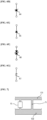
- the reactance adjustment device 16 can use a capacitive reactance element 61 shown in Figure 6A .
- the capacitive reactance element 61 can be a semiconductor diode or other capacitive reactance elements that have the inter-terminal capacitance described above in the DTTB band, for example.
- the reactance adjustment device 16 is configured by only an inductive reactance element 62 shown in Figure 6B , if a DC component is contained in the power inputted from the board input part A, the inductive reactance element 62 short-circuits between the line 13 and the ground part.
- a DC cut capacitor 63 is connected in series to the inductive reactance element 62 as shown in Figure 6C , and thereby it is possible to prevent a short circuit while maintaining an electronic component addition function by the inductive reactance element 62.
- the DC cut capacitor 63 may be arranged between the inductive reactance element 62 and the ground part, or may be arranged between the inductive reactance element 62 and the line 13.
- the additional device 15 and the reactance adjustment device 16 it is possible to use various devices or circuits according to a type of electrical stress.
- a Zener diode 64 shown in Figure 6D it is possible to use, a Zener diode 64 shown in Figure 6D , an ordinary semiconductor diode 65 shown in Figure 6E , a TVS diode 66 shown in Figure 6F , a varistor 67 shown in Figure 6G , or a circuit having an equivalent function to these devices.
- the Zener diode 64 is an element that outputs a constant voltage even when a current changes, and whereas the ordinary semiconductor diode 65 is used in a forward direction, the Zener diode 64 is used in a reverse direction.
- the TVS diode 66 is an element that absorbs a transient voltage by rapidly changing in resistance from high resistance to low resistance when receiving a high transient voltage, and thereby outputs a constant voltage that becomes low.
- the varistor 67 is an element having a current non-linearity, and is an element that guides a surge current to a ground part when the surge current exceeding a steady state instantaneously flows.
- the reactance adjustment device 16 can also be configured by a conductor pattern, with the line.
- the additional device 15 and a reactance pattern 71 may be mounted in parallel between a line 131 and a ground part 132 that are formed of a conductor pattern.
- a width, thickness, and length (distance between the line 131 and the ground part 132) of the reactance pattern 71 are set at such values that impedance is in a complex conjugate relationship to the inter-terminal capacitance of the additional device 15.
- a shape of the reactance pattern 71 is not limited to a linear shape as illustrated, but may be a non-linear shape, or a combination of a pattern in a linear shape and a pattern in a non-linear shape.
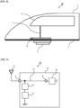
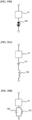
- FIG 8 is a schematic diagram showing a configuration example of the antenna device 30.
- the antenna device 30 has an antenna base 1, and an antenna case 2 that covers the antenna base 1 from above, and is formed of a radio wave transmissive member.
- An accommodation space is formed by the antenna base 1 and the antenna case 2, and the accommodation space is sealed to be watertight.
- the antenna part 11 and the circuit board 12 described above are arranged in the accommodation space.
- the circuit board 12 is fixed to a site corresponding to the attaching part 3 of the antenna base 1.
- the antenna part 11 and the board input part A on the circuit board 12 are conductively connected via a feeder F formed of a coaxial cable, a rod-shaped conductor, or a linear conductor.
- the circuit board 12 is arranged in a front part (left direction to the drawing) of the antenna part 11 in an upward view (a view from the antenna case 2 to the antenna base 1).
- a configuration example shown in Figure 8 is common in the antenna device 10 in Figure 1 and the antenna device 20 in Figure 2 .
- a difference of the antenna device 10 and the antenna device 20 from the antenna device 30 is that in the circuit board 12 of the antenna device 10 and the antenna device 20, the additional device 15 or the reactance adjustment device 16 is not present.
- Arrangement of the circuit board 12 is not limited to the aforementioned example in which the circuit board 12 is arranged in the front part of the antenna part 11 in the upward view.
- the circuit board 12 can only be arranged under the antenna part 11 in a side view that is a view in a direction orthogonal to the upward view. Further, the circuit board 12 does not have to be arranged directly under the antenna part 11, but may be arranged in a position where the board is not covered with the antenna part in a top view, for example.
- FIG. 9 is a schematic diagram showing a configuration example of an antenna device 40 according to the second embodiment, and components having the same functions as the components shown in the first embodiment are assigned with the same reference signs.
- the antenna device 40 has a configuration in which in a circuit board 12, a reactance adjustment device 16 having the same polarity as an additional device 15 is inserted and connected in series between the additional device 15 and the ground part shown in the antenna device 20 in Figure 2 .
- Series impedance of the reactance adjustment device 16 is set at a value that is the same as or larger than the series impedance of the additional device 15.
- the additional device 15 is the same semiconductor diode as in the first embodiment, and an inter-terminal capacitance thereof is 7 pF similar to the inter-terminal capacitance in the first embodiment.
- the reactance adjustment device 16 is a chip capacitor in the second embodiment, and a tip capacitor with a capacity thereof being 5 pF is used.
- the series impedance is obtained by expression of
- ⁇ (R) 2 +(jX) 2 ⁇ .
- the reactance of the additional device 15 at a time of series connection at a time of a frequency being 595 MHz is -j38.3 ( ⁇ ), and since a conductor resistance value R can be ignored as described above, impedance of the additional device 15 at the time of series connection is 38.3 ⁇ .
- the reactance of the reactance adjustment device 165 pF is -j53.6 ⁇ , and impedance is 53.6 ⁇ . From these results, a value of the impedance of the reactance adjustment device 16 is higher than a value of the impedance of the additional device 15.
- the reactance adjustment device 16 is desirably arranged in a position as close as possible to a position where the additional device 15 is arranged.
- Wiring from the additional device 15 to the reactance adjustment device 16 includes inductance and capacitance, so that the shorter the wiring is, the more an influence of the inductance and capacitance can be suppressed.
- an increase in transmission loss is suppressed by arranging the reactance adjustment device 16 in a range within 1/10 wavelength of an upper limit frequency in the DTTB band from the position where the additional device 15 is arranged, as described above.
- a chip capacitor is used as the reactance adjustment device 16, but the reactance adjustment device 16 is not limited to this, and another device having capacitance in the DTTB band or a conductor pattern described later may be used.
- Figure 10A is a Smith chart showing the loci of impedances in the antenna device 20 and the antenna device 40.
- a solid line 901 represents a locus of impedance in the antenna device 20
- a dotted line 902 represents a locus of impedance in the antenna device 40.
- Figure 10B is a VSWR characteristic diagram in the antenna device 20 and the antenna device 40.
- an axis of ordinates represents VSWR
- an axis of abscissas represents a frequency [MHz]
- a solid line 911 represents a VSWR characteristic in the antenna device 20
- an alternate long and short dash line 912 represents a VSWR characteristic in the antenna device 40 in the second embodiment.
- the impedance of the antenna device 20 is capacitive in the DTTB band, and the locus 901 is in a lower half region of the Smith chart.
- the impedance of the antenna device 40 is also capacitive in the DTTB band, and the locus 902 is in the lower half region of the Smith chart.
- a chip capacitor is used as the reactance adjustment device 16, whereby the locus 902 of the impedance of the antenna device 40 is in a position closer to a horizontal axis than the locus 901 of the impedance of the antenna device 20, and matching is achieved more than in the case with only the additional device 15.
- VSWR in the DTTB band of the antenna device 20 increases with the frequency, and a minimum value thereof is 2.7, and a maximum value is 4.3.
- VSWR of the antenna device 40 increases with the frequency, but a minimum value of VSWR is 1.6 whereas a maximum value is 1.9, and VSWR of the antenna device 40 is more remarkably improved than the VSWR of the antenna device 20.
- Figure 11 is a graph showing transmission loss characteristics in the antenna device 20 and the antenna device 40.
- a transmission loss in the antenna device 10 is set as 0 dB.
- a solid line 1001 represents a transmission loss (dB) of the antenna device 20
- a dotted line 1002 represents a transmission loss (dB) of the antenna device 40.
- the transmission loss in the antenna device 20 is -1 dB to -2.1 dB in the DTTB band
- the transmission loss in the antenna device 40 is -0.2 dB to -0.4 dB that is remarkably smaller than the antenna device 20 in the DTTB band. Accordingly, in the antenna device 40, the transmission loss is more reduced than in the antenna device 20.
- Figure 12 is a schematic diagram showing a configuration example of an antenna device 50 according to the third embodiment.
- a reactance adjustment device 16a formed of an inductive reactance element is mounted, instead of the reactance adjustment device 16 formed of a capacitive reactance element shown in Figure 9 .
- the inductive reactance element As the inductive reactance element, a chip inductor in which inductance reaches approximately 47 nH in a center frequency in the DTTB band is used in the present example. However, another inductive reactance element that has similar inductance in the DTTB band or a conductor pattern described later may be used.
- a value of series impedance of the reactance adjustment device 16a is also set equal to or more than a value of series impedance of an additional device 15.
- series impedance of the reactance adjustment device 16a in a frequency of 595 MHz, for example is calculated from the expression of the series impedance described above, the series impedance of the reactance adjustment device 16a is +j175.4 ⁇ , which is higher than the series impedance 38.3 ⁇ of the aforementioned additional device 15.
- Figure 13A is a Smith chart showing frequency characteristics in the antenna device 20 and the antenna device 50.
- a solid line 1201 represents a locus of the impedance in the antenna device 20
- a dotted line 1202 represents a locus of impedance in the antenna device 50.
- Figure 13B is a VSWR characteristic diagram in the antenna device 20 and the antenna device 50 of the third embodiment.
- an axis of ordinates represents VSWR
- an axis of abscissas represents a frequency (MHz)
- a solid line 1211 represents a VSWR characteristic in the antenna device 20
- a dotted line 1212 represents a VSWR characteristic in the antenna device 50 of the third embodiment.
- the impedance of the antenna device 20 is capacitive in the DTTB band, and the locus 1201 thereof is in a lower half region of the Smith chart.
- the impedance of the antenna device 50 is inductive in the DTTB band, the locus 1202 thereof is in an upper half region of the Smith chart, and is closer to a horizontal axis than the locus of the impedance in the antenna device 20.
- VSWR in the antenna device 20 and the antenna device 50 increases with frequency, a minimum value thereof is 2.7 and a maximum value is 4.3, whereas VSWR in the antenna device 50 decreases with frequency, a maximum value thereof is 1.7, and a minimum value is 1.0.
- Figure 14 is a graph showing transmission loss characteristics in the antenna device 20 and the antenna device 50.
- the transmission loss in the antenna device 10 is set as 0 dB.
- a solid line 1301 represents a transmission loss of the antenna device 20.
- the transmission loss is larger than -1 dB, the transmission loss increases as the frequency becomes higher, and a maximum transmission loss is -2.1 dB.
- a dotted line 1302 represents a transmission loss of the antenna device 50.
- the transmission loss in the antenna device 50 is -0.3 dB to -0.1 dB in the DTTB band, and the transmission loss is reduced.
- one end of the additional device 15 is connected to the line 13 connecting the board input part A and the electronic component, the other end is connected to one end of the reactance adjustment device 16, and the other end of the reactance adjustment device 16 is connected to the ground.
- one end of the additional device 15 is connected to the line 13 connecting the board input part A and the electronic circuit 14, the other end is connected to one end of the reactance adjustment device 16a, and the other end of the reactance adjustment device 16a is connected to a ground part.
- Figure 15 is a schematic diagram showing a configuration example of an antenna device 60 according to the fourth embodiment.
- the antenna device 60 differs from the embodiments described so far in that one end of a reactance adjustment device 16 is connected to a line 13 connecting a board input part A and an electronic circuit 14, the other end is connected to one end of an additional device 15, and the other end of the additional device 15 is connected to a ground part.
- the additional device 15 and the reactance adjustment device 16 are arranged by changing positions of the additional device 15 and the reactance adjustment device 16.
- the reactance adjustment device 16 is a chip capacitor of a capacity of 5 pF similarly to the antenna device 40.
- the reactance adjustment device 16 may also be a capacitor, an inductor, or what is formed by arranging a capacitor and an inductor in parallel.
- Figure 16A is a Smith chart showing the loci of impedance in the antenna device 20 and the antenna device 60.
- a solid line 1501 represents a locus of impedance in the antenna device 20, and an alternate long and short dash line 1502 represents a locus of impedance in the antenna device 60.
- Figure 16B is a VSWR characteristic diagram in the antenna device 20 and the antenna device 60.
- an axis of ordinates represents VSWR
- an axis of abscissas represents a frequency [MHz]
- a solid line 1511 represents a VSWR characteristic in the antenna device 20
- an alternate long and short dash line 1512 represents a VSWR characteristic in the antenna device 60.
- the impedance of the antenna device 20 is capacitive in the DTTB band, and the locus is in a lower half region of the Smith chart as shown by the solid line 1501.
- the antenna device 60 is similar to the antenna device 20 in that the impedance of the antenna device 60 is also capacitive in the DTTB band, and the locus is in the lower half region of the Smith chart as shown by the alternate long and short dash line 1502.
- the locus 1502 of the impedance in the antenna device 60 is in a position closer to a horizontal axis than that of the antenna device 20.
- VSWR in the antenna device 20 increases with frequency, and a minimum value thereof is 2.7, whereas a maximum value is 4.3.
- VSWR in the antenna device 60 increases with frequency, but VSWR and fluctuation thereof are smaller than those in the antenna device 20, and a minimum value is 1.6, whereas a maximum value is 1.9.
- Figure 17 is a graph showing transmission loss characteristics in the antenna device 20 and the antenna device 60 of the fourth embodiment.
- the transmission loss in the antenna device 10 is set at 0 dB.
- a solid line 1601 represents a transmission loss characteristic of the antenna device 20
- a dotted line 1602 represents a transmission loss characteristic of the antenna device 60.
- the transmission loss in the DTTB band of the antenna device 20 is -1 to -2.1 dB
- the transmission loss in the DTTB band of the antenna device 60 is -0.2 to -0.4 dB.
- the transmission loss characteristic 1602 in Figure 17 and the transmission loss characteristic 1002 in Figure 11 are substantially the same. From this, it is found that equivalent transmission loss characteristics are obtained in the antenna device 60 and the antenna device 40.
- a fifth embodiment of the present disclosure will be described.
- the reactance adjustment devices 16 and 16a are explained as using capacitance components and inductance components by the chip elements and the conductor patterns.
- an example of a case of using a diode or other semiconductor devices as a reactance adjustment device 16b will be described.
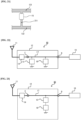
- Figure 18 is a schematic diagram showing a configuration example of an antenna device 70 of the fifth embodiment.
- the reactance adjustment device 16b uses a semiconductor element. As illustrated, in the antenna device 70, the additional device 15 and the reactance adjustment device 16b are connected in series. By this configuration, it is also possible to provide a function of reduction in transmission loss by the reactance adjustment device 16b while making use of the elimination function of electrical stress by the additional device 15.
- Figure 19A is a configuration in which a capacitor 181 as the reactance adjustment device 16b is connected in series to the additional device 15.
- Figure 19B is a configuration in which an inductor 182 as the reactance adjustment device 16b is connected in series to the additional device 15.
- Figure 19C is a configuration in which a diode 183 as the reactance adjustment device 16b is connected in series to the additional device 15.
- Figure 19D is a configuration in which a TVS diode 184 as the reactance adjustment device 16b is connected in series to the additional device 15.
- the filter may be formed of an electronic component, or a wiring pattern.
- Figure 20A and Figure 20B are illustration diagrams of connection aspects of the reactance adjustment device 16.
- Figure 20A is a configuration in which an additional device 15, a capacitor 191, and an inductor 192 are connected in series in this order.
- Figure 20B is a configuration in which a parallel circuit of a capacitor 180 and the inductor 192 is connected in series to the additional device 15. By these configurations, it is possible to suppress a transmission loss in the DTTB band.
- a reactance pattern 211 connects the other end of an additional device 15 having one end connected to a line 131 formed of a conductor pattern, and a ground part 132.
- a width, a thickness, and a length (distance between the other end of the additional device 15 and the ground part 132) of the reactance pattern 211 are set at such values that impedance becomes equivalent to or larger than an inter-terminal capacitance of the additional device 15.
- a polarity of the reactance pattern 211 to the additional device 15 is not particularly limited.
- a shape of the reactance pattern 211 is not limited to a linear shape as illustrated, but may be in a non-linear shape, or a combination of a pattern in a linear shape and a pattern in a non-linear shape.
- the additional device 15 and the reactance adjustment device 16 are arranged on the input side of the circuit board 12, that is, between the board input part A and the circuit input part B is described. This is because the additional device 15 needs to protect the electronic components of the electronic circuit 14 from the electrical stress caused by electric power that is mainly inputted through the antenna part 11.
- the electrical stress may also occur on an output side of the electronic circuit 14.
- external electronic equipment for example, a system unit may be connected to the output side of the electronic circuit 14.
- the system unit supplies a DC voltage for antenna drive to an antenna part 11 via a circuit board 12, and receives a signal (RF signal) in the DTTB band from the circuit board 12. Since in the antenna device for a vehicle, the DC voltage for antenna drive is supplied from a vehicle battery, the DC voltage may fluctuate according to engine ON/OFF and a vehicle driving condition. The fluctuation in the DC voltage becomes electrical stress to the circuit board 12, in particular, the electronic circuit 14.
- an additional device 15 for eliminating such electrical stress, and a reactance adjustment device 16 that is paired with the additional device 15 is arranged.
- FIG 22 is a schematic diagram showing a configuration example of an antenna device 80 according to the sixth embodiment.
- the additional device 15 and the reactance adjustment device 16 are arranged in parallel between an output side of the circuit board 12, that is, a circuit output part C and a board output part D. Since the board output part D is a part to be connected to the external electronic equipment such as a system unit, the board output part D can also be said as the external connection part D to be an interface with external electronic equipment.
- the additional device 15 and the reactance adjustment device 16 are connected in parallel. In other words, one end of the additional device 15 is connected to a line 17 connecting the circuit output part C and the board output part D, and the other end of the additional device 15 is grounded. One end of the reactance adjustment device 16 is also connected to the line 17, and the other end of the reactance adjustment device 16 is grounded.
- the system unit 18 described above is connected to the board output part D.
- Figure 23 is a schematic diagram showing a configuration example of an antenna device 90 that is a modification example of the sixth embodiment.
- an additional device 15 and a reactance adjustment device 16 are connected in series in this order, and the other end of the reactance adjustment device 16 is grounded.
- the other configuration is the same as in Figure 22 .
- the antenna devices 80 and 90 it is possible to exhibit similar effects to the effects of the antenna devices 30 and 40.
- the antenna devices 80 and 90 can suppress an increase in transmission loss while maintaining an elimination operation of the electrical stress by the additional device 15.
- Figure 24A is an example in which a Zener diode 2201 as the additional device 15, and a TVS (transient voltage suppression) diode 2202 as the reactance adjustment device 16 are connected in series.
- a Zener diode 2201 as the additional device 15
- a TVS (transient voltage suppression) diode 2202 as the reactance adjustment device 16 are connected in series.
- the Zener diode 2201 operates when a voltage exceeding a maximum rated voltage of the electronic components of the circuit board 12 is applied as the DC voltage from the system unit 18.
- the Zener diode 2201 generally has inter-terminal capacitance of about several tens pF to several hundreds pF. Therefore, by only using the Zener diode 2201 as the additional device 15 in the DTTB band, a level of a signal (RF signal) outputted from the circuit board 12 to the system unit 18 is significantly attenuated. Therefore, in the configuration example shown in Figure 24A , the TVS diode 2202 is connected in series to the Zener diode 2201, as the reactance adjustment device 16.
- the inter-terminal capacitance of the Zener diode 2201 is 275 pF, and an inter-terminal capacitance of the TVS diode 2202 is 0.35 pF.
- an inter-terminal capacitance at a time of the Zener diode 2201 and the TVS diode 2202 being connected in series is 0.35 pF, which is very small, and it is possible to suppress attenuation of the RF signal.
- the TVS diode 2202 has a function as an overvoltage protection component, and therefore has the advantage of being capable of protecting electronic components by itself in a case where electrical stress of static electricity or the like occurs during handling in a manufacturing line of the antenna device 90 or the circuit board 12, in addition to the operational effects as the reactance adjustment device 16.
- Figure 24A a mode in which the Zener diode 2201 and the TVS diode 2202 are connected in series is shown. In this example, an operation voltage of the protection element rises by the Zener diode and the TVS diode being connected in series.
- Figure 24B an example in which the operation voltage of the protection element is raised by arranging two TVS diodes in series is shown as another mode.
- an advantage of being able to prevent an erroneous operation due to the DC voltage to be supplied, a ripple or the like is obtained since the operation voltages of the protection elements rise.
- Figure 24C is an example in which the Zener diode 2201 and the TVS diode 2202 in the example of Figure 24A are packaged in one container P10.
- an input terminal P11 and an output terminal P12 are mounted, one end of the Zener diode 2201 is connected to the input terminal P11, and the other end is connected to one end of the TVS diode 2202.
- the other end of the TVS diode 2202 is connected to the output terminal P12.
- Zener diode 2201 and the TVS diode 2202 are packaged in the one container P10 like this, it is possible to simplify a manufacturing process as compared with a case of separately incorporating these diodes in the antenna device 90. Further, exchange is also facilitated. Furthermore, it is possible to manufacture the packaged product as an independent protection device. In this case, the usage becomes possible in not only the antenna device 90 but also other electronic devices, and it is possible to increase an application scene of the present disclosure.
- the configuration of packaging in the one container P10 is not limited to the example in Figure 24A and can be similarly adopted for the example in Figure 24B and the additional device 15 and the reactance adjustment device 16 that are described so far.
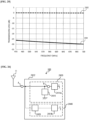
- Figure 25 is a graph showing a transmission loss characteristic in the antenna device 90.
- the transmission loss is a transmission loss from the board output part D to the circuit output part C on the circuit board 12 in the DTTB band.
- the transmission loss in the antenna device 10 is set as 0 dB.
- a solid line 2301 represents a transmission loss in a configuration example in which only the Zener diode 2201 is inserted as the additional device 15 in the antenna device 90, and a maximum loss thereof is -29.9 dB.
- a dotted line 2302 represents a transmission loss in a configuration example in which the Zener diode 2201 and the TVS diode 2202 are connected in series in the antenna device 90, and a maximum transmission loss thereof is 0 dB. From the result, it is found that the transmission loss is significantly suppressed by connecting the Zener diode 2201 and the TVS diode 2202 in series.
- the frequency band in use is the DTTB band
- the present disclosure can also be applied not only in the DTTB band but also in other high frequency bands, for example, a microwave band, or a high frequency band higher than the microwave band, as long as it is a frequency band in which the reactance component of the additional device 15 becomes so large that it cannot be ignored, that is, the frequency band in which the reactance component of the additional device 15 influences the operation of the electronic circuit 14.
- the present disclosure can also be applied in an FM wave band below the microwave band.
- FIG. 26 is a schematic diagram showing a configuration example of an antenna device 100 of the seventh embodiment.
- an FM circuit 2430 and a DTTB circuit 2440 are mounted to one circuit board 2412.
- an antenna part 11 is connected to the circuit board 2412 through a board input part A, and input is divided into the FM circuit 2430 and the DTTB circuit 2440.
- a line is further branched, and one of the branched lines is connected to a circuit input part B on an input side of an electronic circuit 2414a, and the other one is connected to a reactance adjustment device 2416.
- the line is connected to an electronic component 2414b via a filter 2420.
- impedance on a DTTB circuit 2440 side gives electrical stress to the FM circuit 2430.
- the DTTB circuit impedance is a fluctuation element of impedance on an input side of the FM circuit 2430.
- one end of the reactance adjustment device 2416 that is in a complex conjugate relationship with the DTTB circuit impedance added in parallel is connected to an input side of the electronic circuit 2414a of the FM circuit 2430, and the other end is connected to a ground part.
- the reactance adjustment device 2416 cancels electrical stress to be applied to the electronic circuit 2414a of the FM circuit 2430 by itself, and operates to suppress an influence of an impedance fluctuation on an input side of the FM circuit 2430 due to the DTTB circuit impedance. Therefore, it is possible to exhibit similar effects as the effects of the first to the sixth embodiments.
- FIG. 27 is a schematic diagram showing a configuration example of an antenna device 110 according to the eighth embodiment, and the same elements as the elements in Figure 26 are assigned with the same reference signs.
- a system unit 2518 (the same unit as the aforementioned system unit 18) is connected to a board output part D.
- the system unit 2518 supplies a DC voltage for antenna drive to an antenna part 11 (not illustrated) via a circuit board 2512 and receives a signal in the DTTB band (RF signal) and a signal in an FM wave band (FM signal) from the circuit board 2512. Since the DC voltage for antenna drive of the antenna device 110 is supplied from a vehicle battery, the DC voltage may fluctuate depending on engine ON/OFF, and a vehicle driving condition. The fluctuation of the DC voltage becomes electrical stress to respective components of the DTTB circuit 2440 and the FM circuit 2530 of the circuit board 2512.
- one end of a reactance adjustment device 2416 is connected to a line between a circuit output part C on an output side of an electronic circuit 2414a of the FM circuit 2530 and a board output part D, and the other end of the reactance adjustment device 2416 is connected to a ground part.
- the reactance adjustment device 2416 itself eliminates electrical stress to be applied to the electronic circuit 2414a of the FM circuit 2530, and operates to suppress an influence of an impedance fluctuation in an output side of the FM circuit 2530 caused by the DTTB circuit 2440 (DTTB circuit impedance). Therefore, it is possible to exhibit similar effects to the effects of the seventh embodiment.
- an electronic circuit protection device including an electronic circuit, an additional device connected between an input side or an output side of the electronic circuit and a ground part, and adding electrical stress to a component of the electronic circuit, and a reactance adjustment device that cancels reactance of the additional device in a frequency band in use, besides the embodiments as the antenna device 30 and the like.
- the reactance causing the electrical stress is, for example, reactance of an additional device that is connected between the board input part and the ground part, and that eliminates electrical stress to be applied to the component of the electronic circuit.
- the reactance adjustment device cancels the reactance causing the electrical stress, and therefore, an increase in a transmission loss of a signal (power) from the antenna part to the electronic circuit can be suppressed while eliminating the electrical stress.
- the board includes the board input part serving as the input interface with the antenna part and a circuit input part serving as an input interface of the electronic circuit, and the reactance adjustment device is mounted between the board input part and the electronic circuit. According to the configuration, an increase in transmission loss of a signal (power) from the antenna part to the electronic circuit can be suppressed.
- An antenna device including an antenna part, a board to which the antenna part is connected, an electronic circuit mounted to the board, and a reactance adjustment device that cancels reactance in a frequency band in use, the reactance causing electrical stress to be applied to a component of the electronic circuit, wherein the board includes an external connection part to be connected to external electronic equipment, and the reactance adjustment device is mounted between the electronic circuit and the external connection part, and is connected to a ground part.
- the reactance causing the electrical stress is, for example, reactance of an additional device that is connected between the circuit output part and the ground part, and that eliminates electrical stress to be applied to the component of the electronic circuit.
- the reactance adjustment device cancels the reactance causing the electrical stress, and therefore, an increase in transmission loss of a signal (power) from the external electronic equipment to the electronic circuit can be suppressed while eliminating the electrical stress.
- the board includes a circuit output part to be an output side of the electronic circuit and the external connection part to be connected to the external electronic equipment, and the reactance adjustment device is mounted between the circuit output part and the external connection part and is connected to the ground part. According to the configuration, an increase in transmission loss of a signal (power) from the external electronic equipment to the circuit output part of the electronic circuit can be suppressed.
Landscapes
- Engineering & Computer Science (AREA)
- Remote Sensing (AREA)
- Computer Networks & Wireless Communication (AREA)
- Signal Processing (AREA)
- Details Of Aerials (AREA)
- Input Circuits Of Receivers And Coupling Of Receivers And Audio Equipment (AREA)
- Emergency Protection Circuit Devices (AREA)
Abstract
Description
- The present invention relates to an antenna device that is mountable on a moving body or the like and an electronic circuit protection device.
- In a case where electronic components for a plurality of frequency bands are arranged close to one another in one case as in an antenna device for a vehicle, for example, interference between the electronic components may occur, or noise from the outside may enter, and antenna performance as designed may not be able to be obtained. Considering this point,
Patent Literature 1 discloses an antenna device for a vehicle having two antenna elements corresponding to two types of frequency bands, and an attenuation circuit that attenuates a signal of the other frequency band is connected to one of the two antenna elements. - Further,
Patent Literature 2 discloses an antenna device mounted with a protection circuit between an antenna part and an electronic circuit (external connection terminal), one end of the protection circuit being grounded, the other end being connected to a line connecting the antenna part and the electronic circuit. The protection circuit causes a surge current caused by a surge voltage that instantaneously exceeds a steady state to flow to a ground side. - The attenuation circuit and the protection circuit as above normally function as protection devices for eliminating electrical stresses in electronic circuits that are used in environments where the electronic circuits can receive the electrical stresses caused by occurrences of an unintentional electromagnetic field, voltage, and current.
-
- Patent Literature 1:
Japanese Patent Laid-Open No. 2020-136880 - Patent Literature 2:
Japanese Patent Laid-Open No. 2019-125861 - The protection devices described in
Patent Literatures - However, such devices do not directly contribute to signal transmission from an input side to an output side of electronic circuits. Consequently, from a viewpoint of signal transmission, an extra load is added, and depending on a frequency band in use of the electronic circuit, reactance of the protection device may become so large that it cannot be ignored. In particular, in a case where the protection device is added between an antenna part and an electronic circuit, impedance mismatch or power transmission loss increases, and gain characteristics and VSWR characteristics of the antenna part viewed from the electronic circuit side may deteriorate.
- One example of objects of the present disclosure is to make it possible, in an antenna device, to protect components of an electronic circuit used in an environment that can receive electrical stress from such electrical stress, and to relieve an influence on signal transmission. The other objects of the present disclosure will become apparent from the description herein.
- One aspect of the present disclosure is an antenna device including an antenna part, a board to which the antenna part is connected, an electronic circuit mounted to the board, and a reactance adjustment device that cancels reactance in a frequency band in use, the reactance causing electrical stress to be applied to a component of the electronic circuit, wherein the board includes a board input part serving as an input interface with the antenna part, and the reactance adjustment device is mounted between the board input part and the electronic circuit, and is connected to a ground part.
- Another aspect of the present disclosure is an antenna device including an antenna part, a board to which the antenna part is connected, an electronic circuit mounted to the board, and a reactance adjustment device that cancels reactance in a frequency band in use, the reactance causing electrical stress to be applied to a component of the electronic circuit, wherein the board includes an external connection part to be connected to external electronic equipment, and the reactance adjustment device is mounted between the electronic circuit and the external connection part, and is connected to a ground part.
- Another aspect of the present disclosure is an electronic circuit protection device including an electronic circuit, an additional device that is connected between an input side or an output side of the electronic circuit, and a ground part, and is added to protect a component of the electronic circuit from electrical stress, and a reactance adjustment device that cancels reactance of the additional device in a frequency band in use.
- According to the above-described aspects, it is possible to protect the components of the electronic circuit from electrical stress, and to relieve an influence on signal transmission.
-
- [
Figure 1] Figure 1 is a schematic diagram showing a basic configuration example of an antenna device to which the present disclosure can be applied. - [
Figure 2] Figure 2 is a schematic diagram showing a configuration example of an antenna device having only an additional device. - [
Figure 3] Figure 3 is a schematic diagram showing a configuration example of an antenna device according to a first embodiment in which a reactance adjustment device is mounted. - [
Figure 4A] Figure 4A is a Smith chart representing the loci of impedances in the reactance adjustment device itself, and the antenna devices inFigure 2 and Figure 3 . - [
Figure 4B] Figure 4B is a VSWR characteristic diagram in the reactance adjustment device itself, and the antenna devices inFigure 2 and Figure 3 . - [
Figure 5] Figure 5 is a graph representing transmission loss characteristics in the antenna devices inFigure 2 and Figure 3 . - [
Figure 6A] Figure 6A is a diagram showing a specific example of the reactance adjustment device. - [
Figure 6B] Figure 6B is a diagram showing a specific example of the reactance adjustment device. - [
Figure 6C] Figure 6C is a diagram showing a specific example of the reactance adjustment device. - [
Figure 6D] Figure 6D is a diagram showing a specific example of the reactance adjustment device. - [
Figure 6E] Figure 6E is a diagram showing a specific example of the reactance adjustment device. - [
Figure 6F] Figure 6F is a diagram showing a specific example of the reactance adjustment device. - [
Figure 6G] Figure 6G is a diagram showing a specific example of the reactance adjustment device. - [
Figure 7] Figure 7 is a view showing an example in which the reactance adjustment device is configured by a conductor pattern. - [
Figure 8] Figure 8 is a schematic diagram showing an arrangement structure example of each of components of the antenna device according to the first embodiment. - [
Figure 9] Figure 9 is a schematic diagram showing a configuration example of an antenna device according to a second embodiment. - [
Figure 10A] Figure 10A is a Smith chart representing the loci of impedances in the antenna devices inFigure 2 andFigure 9 . - [
Figure 10B] Figure 10B is a VSWR characteristics diagram in the antenna devices inFigure 2 andFigure 9 . - [
Figure 11] Figure 11 is a graph representing transmission loss characteristics in the antenna devices inFigure 2 andFigure 9 . - [
Figure 12] Figure 12 is a schematic diagram showing a configuration example of an antenna device according to a third embodiment. - [
Figure 13A] Figure 13A is a Smith chart representing the loci of impedances in the antenna devices inFigure 2 andFigure 12 . - [
Figure 13B] Figure 13B is a VSWR characteristics chart of the antenna devices inFigure 2 andFigure 12 . - [
Figure 14] Figure 14 is a graph representing transmission loss characteristics in the antenna devices inFigure 2 andFigure 12 . - [
Figure 15] Figure 15 is a schematic diagram showing a configuration example of an antenna device according to a fourth embodiment. - [
Figure 16A] Figure 16A is a VSWR characteristics diagram in the antenna devices inFigure 2 andFigure 15 . - [
Figure 16B] Figure 16B is a VSWR characteristics diagram in the antenna devices inFigure 2 andFigure 15 . - [
Figure 17] Figure 17 is a graph representing transmission loss characteristics comparing a case with only a Zener diode and a case with a Zener diode and a TVS diode in the antenna device of the fourth embodiment. - [
Figure 18] Figure 18 is a schematic diagram showing a configuration example of an antenna device according to a fifth embodiment. - [
Figure 19A] Figure 19A is an illustration diagram of an alternative configuration of a reactance adjustment device. - [
Figure 19B] Figure 19B is an illustration diagram of an alternative configuration of the reactance adjustment device. - [
Figure 19C] Figure 19C is an illustration diagram of an alternative configuration of the reactance adjustment device. - [
Figure 19D] Figure 19D is an illustration diagram of an alternative configuration of the reactance adjustment device. - [
Figure 20A] Figure 20A is an illustration diagram of a connection aspect of the reactance adjustment device. - [
Figure 20B] Figure 20B is an illustration diagram of a connection aspect of the reactance adjustment device. - [
Figure 21] Figure 21 is a view showing another example in which the reactance adjustment device is configured by a conductor pattern. - [
Figure 22] Figure 22 is a schematic diagram showing a configuration example of an antenna device according to a sixth embodiment. - [
Figure 23] Figure 23 is a schematic diagram showing a configuration example of an antenna device of a modification example of the sixth embodiment. - [
Figure 24A] Figure 24A is an explanatory diagram showing specific examples of an additional device and a reactance adjustment device according to the sixth embodiment. - [
Figure 24B] Figure 24B is an explanatory diagram showing specific examples of the additional device and the reactance adjustment device according to the sixth embodiment. - [
Figure 24C] Figure 24C is an explanatory diagram showing specific examples of the additional device and the reactance adjustment device according to the sixth embodiment. - [
Figure 25] Figure 25 is a graph representing a transmission loss in which a case with only a Zener diode and a case with the Zener diode and a TVS diode in the antenna device according to the sixth embodiment are compared. - [
Figure 26] Figure 26 is a schematic diagram showing a configuration example of an antenna device according to a seventh embodiment. - [
Figure 27] Figure 27 is a schematic diagram showing a configuration example of an antenna device according to an eighth embodiment. - Hereinafter, embodiment examples in a case of carrying out the present disclosure as an antenna device that is mounted to a moving body such as a vehicle will be described. The antenna device receives signals from 470 MHz to 720 MHz that are in a DTTB (Digital Television Terrestrial Broadcasting System) band.
- First, a basic configuration example of an antenna device to which the present disclosure can be applied is shown in
Figure 1 . Anantenna device 10 shown inFigure 1 is configured by accommodating anantenna part 11 and acircuit board 12 in an antenna case described later and attached to a vehicle roof or the like. Theantenna part 11 is configured by a planar conductor, a linear (including rod-shaped) conductor or a conductor in which these conductors are combined, which resonates in the DTTB band. On thecircuit board 12, a board input part A to be an input interface with theantenna part 11, and a circuit input part B to be an input interface of anelectronic circuit 14 are mounted. In theelectronic circuit 14, electronic components including active elements such as transistors and diodes are implemented. The board input part A and the circuit input part B are electrically connected with aline 13 such as a conductor pattern. - What is arranged between the board input part A and the circuit input part B is not limited to a conductor pattern. One or a plurality of circuits may be arranged between the board input part A and the circuit input part B, for example, either one or both of an
additional device 15 described later and areactance pattern 211 may be arranged. - It is assumed that in the DTTB band, a characteristic impedance at a time of an
antenna part 11 side being seen from the board input part A is 50 Ω in the present example, and an impedance at a time of anelectronic circuit 14 side being seen from the circuit input part B is also 50 Ω in the present example. In this case, if an impedance of theline 13 between the board input part A and the circuit input part B is also 50 Ω, the impedances in a system to theelectronic circuit 14 from theantenna part 11 are matched and a transmission loss of power (signal level) at a time of signal transmission hardly occurs. - The
electronic circuit 14 is configured by including the plurality of electronic components described above, and these electronic components include many electronic components that are vulnerable to the aforementioned electrical stress. Therefore, in a case where antenna parts for other frequency bands, electronic circuits, and the like are closely arranged in the antenna case, a strong transmission wave is outputted from an antenna device mounted to another vehicle traveling in a vicinity, or a surge exceeding a steady state instantaneously occurs, theelectronic circuit 14 is severely influenced, even if it is an electromagnetic wave or voltage at a frequency different from the DTTB band. Therefore, in the first embodiment, theadditional device 15 for eliminating electrical stress is mounted in a front stage of theelectronic circuit 14 as in anantenna device 20 shown inFigure 2 . - The
additional device 15 is a semiconductor diode with two terminals in the present example, one end thereof is connected to theline 13, and the other end is connected to a ground part. - The
additional device 15 has capacitance (capacitive reactance) that is inter-terminal capacitance. The inter-terminal capacitance is about 0.2 pF to 30 pF depending on a type of the semiconductor diode, and is 7 pF in the DTTB band in the case of the present example. When a shunt connection of theadditional device 15 like this to theline 13 is performed, electrical stress given to the components of theelectronic circuit 14 is eliminated, but the component unnecessary to the function of signal transmission is added, so that impedance mismatch always occurs between theantenna part 11 and theelectronic circuit 14 in the DTTB band. In other words, the impedance at the time of theelectronic circuit 14 side being seen from the board input part A becomes capacitive in the DTTB band, and transmission loss of power that is transmitted from the board input part A to the circuit input part B increases. Therefore, an antenna gain is reduced. - Thus, in the first embodiment, as in an
antenna device 30 inFigure 3 , areactance adjustment device 16 that cancels a fluctuation in reactance caused by the presence of theadditional device 15 is mounted in parallel with theadditional device 15 while making use of the electrical stress elimination operation by theadditional device 15. Thereactance adjustment device 16 is an inductive reactance element having inductance of 10.2 nH in the DTTB band in the present example, one end thereof is connected to theline 13, and the other end is connected to a ground part. By thereactance adjustment device 16, a fluctuation to capacitance, of impedance when using a semiconductor diode as theadditional device 15 is eliminated. - A type and a mode of the inductive reactance element may be arbitrary, but by using a chip inductor, the inductive reactance element becomes compacter (thinner) than a coil, and has an advantage that even when it is implemented in the
circuit board 12 with theadditional device 15, a design size of thecircuit board 12 does not have to be changed. - The inductive reactance element may be configured by a combination of a plurality of conductor patterns instead of the chip inductor.
- Inductance of the
reactance adjustment device 16 is desirably set so that a reactance component of the inductance is in a complex conjugate relationship to the inter-terminal capacitance of theadditional device 15. "Complex conjugate" means that the polarities are opposite and the magnitudes are equal. - In other words, the "complex conjugate relationship" means a relationship in which when reactance of the
additional device 15 is jX, reactance of thereactance adjustment device 16 is +jX. Thereby, capacitive reactance of theadditional device 15 in the DTTB band is cancelled by inductive reactance of thereactance adjustment device 16, and impedance between the board input part A and the circuit input part B becomes 50 Ω. Showing in a numerical value example specifically, while the capacitive reactance of theadditional device 15 is approximately -j24.1 (Ω) in the frequency of 595 MHz, the inductive reactance of thereactance adjustment device 16 is +j24.1 (Ω), and the impedances are in a complex conjugate relationship. - The
reactance adjustment device 16 is arranged at a position as close as possible to an arrangement position of theadditional device 15. Thereby, it is possible to suppress inductance and capacitance of theline 13 from theadditional device 15 to thereactance adjustment device 16. Preferably, thereactance adjustment device 16 is arranged in a range within 1/10 wavelength of the highest frequency in the DTTB band from the position in which theadditional device 15 is arranged. Thereby, it is possible to further reduce the influence of inductance and capacitance of theline 13. - Next, an antenna characteristic of the
antenna device 30 according to the first embodiment will be described.Figure 4A is a Smith chart showing the loci of impedances in thereactance adjustment device 16 alone, and theantenna device 20 and theantenna device 30. As is known, an upper half region of the Smith chart shows inductivity, and a lower half region shows capacitance. In the drawing, asolid line 401 shows a locus of impedance in theantenna device 20, an alternate long andshort dash line 402 shows a locus of the impedance in theantenna device 30, and adotted line 403 shows a locus of the impedance in thereactance adjustment device 16 alone. At a position of 1.0 of the Smith chart center, impedances between theantenna part 11 and theelectronic component 14 are matched, and a transmission loss becomes the smallest. Accordingly, in order to minimize the transmission loss between theantenna part 11 and theelectronic component 14 in the DTTB band, it is preferable to satisfy a condition that the locus of the impedance passes through the position of 1.0 of the Smith chart center. The above is a common content in the Smith chart used in the present specification. - As shown in
Figure 4A , thelocus 403 of the impedance in thereactance adjustment device 16 alone is inductive throughout an entire region of the DTTB band as a matter of course. Thelocus 401 of the impedance of theantenna device 20 is capacitive throughout the entire region of the DTTB band. Further, thelocus 401 of the impedance is substantially symmetrical about a horizontal axis with thelocus 403 of the impedance in thereactance adjustment device 16 alone, and is in the lower half region of the Smith chart. On the other hand, thelocus 402 of the impedance in theantenna device 30 passes through the horizontal axis in a vicinity of 1.0 of the Smith chart center. - In this way, the
antenna device 30 having thereactance adjustment device 16 having a complex conjugate relationship to the inter-terminal capacitance of theadditional device 15 reduces the transmission loss caused by the presence of theadditional device 15. -
Figure 4B is a VSWR characteristic diagram in theantenna device 20 and theantenna device 30. In the drawing, an axis of ordinates represents VSWR, and an axis of abscissas represents a frequency (MHz). Asolid line 411 represents a VSWR characteristic in theantenna device 20, and an alternate long andshort dash line 412 represents a VSWR characteristic in theantenna device 30. As shown in thesolid line 411 inFigure 4B , the VSWR in theantenna device 20 becomes larger substantially rectilinearly as the frequency becomes higher, and the minimum value thereof is 2.7, whereas a maximum value is 4.3. In contrast to this, as shown in the alternate long andshort dash line 412 inFigure 4B , the VSWR of theantenna device 30 reaches a minimum value 1.0 in a vicinity of a frequency 600 MHz, and a maximum value thereof is 1.9. - In this way, in the
antenna device 30 having thereactance adjustment device 16 that has impedance in a complex conjugate relationship to the inter-terminal capacitance of theadditional device 15, VSWR is less than 2 in all frequencies in the DTTB band. -
Figure 5 is a graph representing transmission loss characteristics in theantenna device 20 and theantenna device 30. In this graph, a transmission loss in theantenna device 10 shown inFigure 1 is set as 0 dB. In the drawing, asolid line 501 represents a transmission loss (dB) by the configuration of theantenna device 20. In the configuration of theantenna device 20, the transmission loss is larger than -1 dB throughout an entire region of the DTTB band. Further, as the frequency becomes higher, the transmission loss becomes larger, and a transmission loss in the vicinity of 720 MHz which is an upper limit frequency in the DTTB band reaches -2.1 dB. An alternate long andshort dash line 502 represents a transmission loss (dB) of theantenna device 30. The transmission loss in theantenna device 30 is substantially 0 dB throughout a substantially entire region of the DTTB band, a fluctuation by the frequency is also small, and the transmission loss is about -0.4 dB at a maximum. - This is considered to be because in the
antenna device 20 in which only theadditional device 15 is mounted, a degree of impedance mismatch increases as a frequency in use becomes higher. In contrast to this, in theantenna device 30 in which thereactance adjustment device 16 is mounted in parallel with theadditional device 15, it is possible to cancel a fluctuation in impedance caused by mounting theadditional device 15, even if the reactance of theadditional device 15 fluctuates with a change in the frequency in use, because thereactance adjustment device 16 cancels the reactance that is fluctuated. Therefore, in theantenna device 30, it is possible to effectively suppress impedance mismatch and increase in transmission loss of power while maintaining an elimination operation of electrical stress of theadditional device 15. - In the first embodiment, a description is made based on the premise that the
additional device 15 is a semiconductor diode, that is, theadditional device 15 generates capacitive reactance in the DTTB band. However, theadditional device 15 may be a device that inductively changes the impedance from the board input part A to the circuit input part B, for example, an inductor. In this case, thereactance adjustment device 16 can use acapacitive reactance element 61 shown inFigure 6A . Thecapacitive reactance element 61 can be a semiconductor diode or other capacitive reactance elements that have the inter-terminal capacitance described above in the DTTB band, for example. By arranging thecapacitive reactance element 61 in parallel with theadditional device 15, it is possible to suppress an increase in transmission loss of power from the board input part A to the circuit input part B. - Further, in a case where the
reactance adjustment device 16 is configured by only aninductive reactance element 62 shown inFigure 6B , if a DC component is contained in the power inputted from the board input part A, theinductive reactance element 62 short-circuits between theline 13 and the ground part. Thus, in an application in which the inputted power may contain a DC component, aDC cut capacitor 63 is connected in series to theinductive reactance element 62 as shown inFigure 6C , and thereby it is possible to prevent a short circuit while maintaining an electronic component addition function by theinductive reactance element 62. In this case, the DC cutcapacitor 63 may be arranged between theinductive reactance element 62 and the ground part, or may be arranged between theinductive reactance element 62 and theline 13. - At the
additional device 15 and thereactance adjustment device 16, it is possible to use various devices or circuits according to a type of electrical stress. For example, it is possible to use, aZener diode 64 shown inFigure 6D , anordinary semiconductor diode 65 shown inFigure 6E , aTVS diode 66 shown inFigure 6F , avaristor 67 shown inFigure 6G , or a circuit having an equivalent function to these devices. - The
Zener diode 64 is an element that outputs a constant voltage even when a current changes, and whereas theordinary semiconductor diode 65 is used in a forward direction, theZener diode 64 is used in a reverse direction. TheTVS diode 66 is an element that absorbs a transient voltage by rapidly changing in resistance from high resistance to low resistance when receiving a high transient voltage, and thereby outputs a constant voltage that becomes low. Thevaristor 67 is an element having a current non-linearity, and is an element that guides a surge current to a ground part when the surge current exceeding a steady state instantaneously flows. - Further, the
reactance adjustment device 16 can also be configured by a conductor pattern, with the line. For example, as shown inFigure 7 , theadditional device 15 and areactance pattern 71 may be mounted in parallel between aline 131 and aground part 132 that are formed of a conductor pattern. A width, thickness, and length (distance between theline 131 and the ground part 132) of thereactance pattern 71 are set at such values that impedance is in a complex conjugate relationship to the inter-terminal capacitance of theadditional device 15. A shape of thereactance pattern 71 is not limited to a linear shape as illustrated, but may be a non-linear shape, or a combination of a pattern in a linear shape and a pattern in a non-linear shape. - Next, an arrangement structure of each component in the
antenna device 30 will be described.Figure 8 is a schematic diagram showing a configuration example of theantenna device 30. Theantenna device 30 has anantenna base 1, and anantenna case 2 that covers theantenna base 1 from above, and is formed of a radio wave transmissive member. An accommodation space is formed by theantenna base 1 and theantenna case 2, and the accommodation space is sealed to be watertight. Theantenna part 11 and thecircuit board 12 described above are arranged in the accommodation space. On theantenna base 1, an attachingpart 3 for attaching theantenna device 30 to a vehicle roof or the like is mounted. - The
circuit board 12 is fixed to a site corresponding to the attachingpart 3 of theantenna base 1. Theantenna part 11 and the board input part A on thecircuit board 12 are conductively connected via a feeder F formed of a coaxial cable, a rod-shaped conductor, or a linear conductor. In this example, thecircuit board 12 is arranged in a front part (left direction to the drawing) of theantenna part 11 in an upward view (a view from theantenna case 2 to the antenna base 1). A configuration example shown inFigure 8 is common in theantenna device 10 inFigure 1 and theantenna device 20 inFigure 2 . A difference of theantenna device 10 and theantenna device 20 from theantenna device 30 is that in thecircuit board 12 of theantenna device 10 and theantenna device 20, theadditional device 15 or thereactance adjustment device 16 is not present. Arrangement of thecircuit board 12 is not limited to the aforementioned example in which thecircuit board 12 is arranged in the front part of theantenna part 11 in the upward view. Thecircuit board 12 can only be arranged under theantenna part 11 in a side view that is a view in a direction orthogonal to the upward view. Further, thecircuit board 12 does not have to be arranged directly under theantenna part 11, but may be arranged in a position where the board is not covered with the antenna part in a top view, for example. - Next, a second embodiment of the preset disclosure will be described.
Figure 9 is a schematic diagram showing a configuration example of an antenna device 40 according to the second embodiment, and components having the same functions as the components shown in the first embodiment are assigned with the same reference signs. The antenna device 40 has a configuration in which in acircuit board 12, areactance adjustment device 16 having the same polarity as anadditional device 15 is inserted and connected in series between theadditional device 15 and the ground part shown in theantenna device 20 inFigure 2 . - Series impedance of the
reactance adjustment device 16 is set at a value that is the same as or larger than the series impedance of theadditional device 15. Thereby, impedance between aline 13 and a ground part increases to eliminate inflow of power, so that it is possible to suppress an increase in transmission loss between a board input part A and a circuit input part B. - In the present example, the
additional device 15 is the same semiconductor diode as in the first embodiment, and an inter-terminal capacitance thereof is 7 pF similar to the inter-terminal capacitance in the first embodiment. On the other hand, thereactance adjustment device 16 is a chip capacitor in the second embodiment, and a tip capacitor with a capacity thereof being 5 pF is used. - A condition of series impedance for suppressing or reducing an increase in transmission loss while cancelling a fluctuation in impedance at the
line 13 due to addition of therespective devices additional device 15 and thereactance adjustment device 16 are connected in series as shown inFigure 9 will be described. Here, for convenience, it is assumed that conductor resistance values of therespective devices - The series impedance is obtained by expression of |Z| = √{(R)2+(jX)2}. The reactance of the
additional device 15 at a time of series connection at a time of a frequency being 595 MHz is -j38.3 (Ω), and since a conductor resistance value R can be ignored as described above, impedance of theadditional device 15 at the time of series connection is 38.3 Ω. Similarly, the reactance of the reactance adjustment device 165 pF is -j53.6 Ω, and impedance is 53.6 Ω. From these results, a value of the impedance of thereactance adjustment device 16 is higher than a value of the impedance of theadditional device 15. - From a viewpoint of component arrangement, the
reactance adjustment device 16 is desirably arranged in a position as close as possible to a position where theadditional device 15 is arranged. Wiring from theadditional device 15 to thereactance adjustment device 16 includes inductance and capacitance, so that the shorter the wiring is, the more an influence of the inductance and capacitance can be suppressed. According to simulation, it is found that an increase in transmission loss is suppressed by arranging thereactance adjustment device 16 in a range within 1/10 wavelength of an upper limit frequency in the DTTB band from the position where theadditional device 15 is arranged, as described above. - In the second embodiment, a chip capacitor is used as the
reactance adjustment device 16, but thereactance adjustment device 16 is not limited to this, and another device having capacitance in the DTTB band or a conductor pattern described later may be used. - Next, an antenna characteristic of the antenna device 40 according to the second embodiment will be described.
Figure 10A is a Smith chart showing the loci of impedances in theantenna device 20 and the antenna device 40. InFigure 10A , asolid line 901 represents a locus of impedance in theantenna device 20, and adotted line 902 represents a locus of impedance in the antenna device 40.Figure 10B is a VSWR characteristic diagram in theantenna device 20 and the antenna device 40. InFigure 10B , an axis of ordinates represents VSWR, and an axis of abscissas represents a frequency [MHz], asolid line 911 represents a VSWR characteristic in theantenna device 20, and an alternate long andshort dash line 912 represents a VSWR characteristic in the antenna device 40 in the second embodiment. - As shown in
Figure 10A , the impedance of theantenna device 20 is capacitive in the DTTB band, and thelocus 901 is in a lower half region of the Smith chart. The impedance of the antenna device 40 is also capacitive in the DTTB band, and thelocus 902 is in the lower half region of the Smith chart. However, in the antenna device 40, a chip capacitor is used as thereactance adjustment device 16, whereby thelocus 902 of the impedance of the antenna device 40 is in a position closer to a horizontal axis than thelocus 901 of the impedance of theantenna device 20, and matching is achieved more than in the case with only theadditional device 15. - Further, as shown by the
solid line 911 inFigure 10B , VSWR in the DTTB band of theantenna device 20 increases with the frequency, and a minimum value thereof is 2.7, and a maximum value is 4.3. On the other hand, as shown in the alternate long andshort dash line 912 inFigure 10B , VSWR of the antenna device 40 increases with the frequency, but a minimum value of VSWR is 1.6 whereas a maximum value is 1.9, and VSWR of the antenna device 40 is more remarkably improved than the VSWR of theantenna device 20. - A similar tendency is also seen concerning the transmission loss characteristics. That is to say,
Figure 11 is a graph showing transmission loss characteristics in theantenna device 20 and the antenna device 40. In this graph, a transmission loss in theantenna device 10 is set as 0 dB. In the drawing, asolid line 1001 represents a transmission loss (dB) of theantenna device 20, and a dottedline 1002 represents a transmission loss (dB) of the antenna device 40. The transmission loss in theantenna device 20 is -1 dB to -2.1 dB in the DTTB band, whereas the transmission loss in the antenna device 40 is -0.2 dB to -0.4 dB that is remarkably smaller than theantenna device 20 in the DTTB band. Accordingly, in the antenna device 40, the transmission loss is more reduced than in theantenna device 20. - A third embodiment of the present disclosure will be described.
Figure 12 is a schematic diagram showing a configuration example of anantenna device 50 according to the third embodiment. In theantenna device 50, areactance adjustment device 16a formed of an inductive reactance element is mounted, instead of thereactance adjustment device 16 formed of a capacitive reactance element shown inFigure 9 . - As the inductive reactance element, a chip inductor in which inductance reaches approximately 47 nH in a center frequency in the DTTB band is used in the present example. However, another inductive reactance element that has similar inductance in the DTTB band or a conductor pattern described later may be used.
- In the third embodiment, a value of series impedance of the
reactance adjustment device 16a is also set equal to or more than a value of series impedance of anadditional device 15. When series impedance of thereactance adjustment device 16a in a frequency of 595 MHz, for example, is calculated from the expression of the series impedance described above, the series impedance of thereactance adjustment device 16a is +j175.4 Ω, which is higher than the series impedance 38.3 Ω of the aforementionedadditional device 15. - Next, an antenna characteristic of the
antenna device 50 according to the third embodiment will be described.Figure 13A is a Smith chart showing frequency characteristics in theantenna device 20 and theantenna device 50. In the drawing, asolid line 1201 represents a locus of the impedance in theantenna device 20, and a dottedline 1202 represents a locus of impedance in theantenna device 50.Figure 13B is a VSWR characteristic diagram in theantenna device 20 and theantenna device 50 of the third embodiment. In this diagram, an axis of ordinates represents VSWR, an axis of abscissas represents a frequency (MHz), asolid line 1211 represents a VSWR characteristic in theantenna device 20, and a dottedline 1212 represents a VSWR characteristic in theantenna device 50 of the third embodiment. - As shown in
Figure 13A , the impedance of theantenna device 20 is capacitive in the DTTB band, and thelocus 1201 thereof is in a lower half region of the Smith chart. On the other hand, the impedance of theantenna device 50 is inductive in the DTTB band, thelocus 1202 thereof is in an upper half region of the Smith chart, and is closer to a horizontal axis than the locus of the impedance in theantenna device 20. - Further, as shown in
Figure 13B , VSWR in theantenna device 20 and theantenna device 50 increases with frequency, a minimum value thereof is 2.7 and a maximum value is 4.3, whereas VSWR in theantenna device 50 decreases with frequency, a maximum value thereof is 1.7, and a minimum value is 1.0. -
Figure 14 is a graph showing transmission loss characteristics in theantenna device 20 and theantenna device 50. In this graph, the transmission loss in theantenna device 10 is set as 0 dB. In the drawing, asolid line 1301 represents a transmission loss of theantenna device 20. In theantenna device 20, the transmission loss is larger than -1 dB, the transmission loss increases as the frequency becomes higher, and a maximum transmission loss is -2.1 dB. A dottedline 1302 represents a transmission loss of theantenna device 50. The transmission loss in theantenna device 50 is -0.3 dB to -0.1 dB in the DTTB band, and the transmission loss is reduced. - In the antenna device 40 of the second embodiment, one end of the
additional device 15 is connected to theline 13 connecting the board input part A and the electronic component, the other end is connected to one end of thereactance adjustment device 16, and the other end of thereactance adjustment device 16 is connected to the ground. Similarly, also in theantenna device 50 of the third embodiment, one end of theadditional device 15 is connected to theline 13 connecting the board input part A and theelectronic circuit 14, the other end is connected to one end of thereactance adjustment device 16a, and the other end of thereactance adjustment device 16a is connected to a ground part. However, it is possible to obtain similar effects even if theadditional device 15 and the reactance adjustment device 16 (or thereactance adjustment device 16a) are arranged by changing the order of these devices. - A fourth embodiment of the present disclosure will be described.
Figure 15 is a schematic diagram showing a configuration example of an antenna device 60 according to the fourth embodiment. The antenna device 60 differs from the embodiments described so far in that one end of areactance adjustment device 16 is connected to aline 13 connecting a board input part A and anelectronic circuit 14, the other end is connected to one end of anadditional device 15, and the other end of theadditional device 15 is connected to a ground part. - In other words, the
additional device 15 and thereactance adjustment device 16 are arranged by changing positions of theadditional device 15 and thereactance adjustment device 16. Thereactance adjustment device 16 is a chip capacitor of a capacity of 5 pF similarly to the antenna device 40. In the antenna device 60, thereactance adjustment device 16 may also be a capacitor, an inductor, or what is formed by arranging a capacitor and an inductor in parallel. -
Figure 16A is a Smith chart showing the loci of impedance in theantenna device 20 and the antenna device 60. In the drawing, asolid line 1501 represents a locus of impedance in theantenna device 20, and an alternate long andshort dash line 1502 represents a locus of impedance in the antenna device 60.Figure 16B is a VSWR characteristic diagram in theantenna device 20 and the antenna device 60. In the drawing, an axis of ordinates represents VSWR, an axis of abscissas represents a frequency [MHz], asolid line 1511 represents a VSWR characteristic in theantenna device 20, and an alternate long andshort dash line 1512 represents a VSWR characteristic in the antenna device 60. - As shown in
Figure 16A , the impedance of theantenna device 20 is capacitive in the DTTB band, and the locus is in a lower half region of the Smith chart as shown by thesolid line 1501. The antenna device 60 is similar to theantenna device 20 in that the impedance of the antenna device 60 is also capacitive in the DTTB band, and the locus is in the lower half region of the Smith chart as shown by the alternate long andshort dash line 1502. However, by connecting thereactance adjustment device 16 to theline 13, and connecting thereactance adjustment device 16 to theadditional device 15 in series, thelocus 1502 of the impedance in the antenna device 60 is in a position closer to a horizontal axis than that of theantenna device 20. - Further, as shown by the
solid line 1511 inFigure 16B , VSWR in theantenna device 20 increases with frequency, and a minimum value thereof is 2.7, whereas a maximum value is 4.3. On the other hand, as shown by thesolid line 1512 inFigure 16B , VSWR in the antenna device 60 increases with frequency, but VSWR and fluctuation thereof are smaller than those in theantenna device 20, and a minimum value is 1.6, whereas a maximum value is 1.9. -
Figure 17 is a graph showing transmission loss characteristics in theantenna device 20 and the antenna device 60 of the fourth embodiment. In this graph, the transmission loss in theantenna device 10 is set at 0 dB. In the drawing, asolid line 1601 represents a transmission loss characteristic of theantenna device 20, and a dottedline 1602 represents a transmission loss characteristic of the antenna device 60. The transmission loss in the DTTB band of theantenna device 20 is -1 to -2.1 dB, and the transmission loss in the DTTB band of the antenna device 60 is -0.2 to -0.4 dB. In this way, it is found that in the antenna device 60, transmission loss of power is more reduced than in theantenna device 20. Further, the transmission loss characteristic 1602 inFigure 17 and the transmission loss characteristic 1002 inFigure 11 are substantially the same. From this, it is found that equivalent transmission loss characteristics are obtained in the antenna device 60 and the antenna device 40. - A fifth embodiment of the present disclosure will be described. In the explanation so far, the
reactance adjustment devices reactance adjustment device 16b will be described. -
Figure 18 is a schematic diagram showing a configuration example of anantenna device 70 of the fifth embodiment. Thereactance adjustment device 16b uses a semiconductor element. As illustrated, in theantenna device 70, theadditional device 15 and thereactance adjustment device 16b are connected in series. By this configuration, it is also possible to provide a function of reduction in transmission loss by thereactance adjustment device 16b while making use of the elimination function of electrical stress by theadditional device 15. - Alternative configuration examples of the
reactance adjustment device 16b are shown inFigure 19A to Figure 19D .Figure 19A is a configuration in which acapacitor 181 as thereactance adjustment device 16b is connected in series to theadditional device 15.Figure 19B is a configuration in which aninductor 182 as thereactance adjustment device 16b is connected in series to theadditional device 15.Figure 19C is a configuration in which adiode 183 as thereactance adjustment device 16b is connected in series to theadditional device 15.Figure 19D is a configuration in which aTVS diode 184 as thereactance adjustment device 16b is connected in series to theadditional device 15. - Further, even if a filter configuration that passes only the DTTB band, or a band-rejection filter configuration that inhibits passage of external noise frequencies, a high frequency component of static electricity or the like is used as another mode of the
reactance adjustment device 16b, it is also possible to similarly suppress a transmission loss in the DTTB band. The filter may be formed of an electronic component, or a wiring pattern. -
Figure 20A and Figure 20B are illustration diagrams of connection aspects of thereactance adjustment device 16.Figure 20A is a configuration in which anadditional device 15, acapacitor 191, and aninductor 192 are connected in series in this order.Figure 20B is a configuration in which a parallel circuit of acapacitor 180 and theinductor 192 is connected in series to theadditional device 15. By these configurations, it is possible to suppress a transmission loss in the DTTB band. - It is also possible to configure the
reactance adjustment devices Figure 21 , it is possible to adopt a configuration in which areactance pattern 211 connects the other end of anadditional device 15 having one end connected to aline 131 formed of a conductor pattern, and aground part 132. A width, a thickness, and a length (distance between the other end of theadditional device 15 and the ground part 132) of thereactance pattern 211 are set at such values that impedance becomes equivalent to or larger than an inter-terminal capacitance of theadditional device 15. A polarity of thereactance pattern 211 to theadditional device 15 is not particularly limited. A shape of thereactance pattern 211 is not limited to a linear shape as illustrated, but may be in a non-linear shape, or a combination of a pattern in a linear shape and a pattern in a non-linear shape. - In each of the first to the fifth embodiments, the example in which the
additional device 15 and thereactance adjustment device 16 are arranged on the input side of thecircuit board 12, that is, between the board input part A and the circuit input part B is described. This is because theadditional device 15 needs to protect the electronic components of theelectronic circuit 14 from the electrical stress caused by electric power that is mainly inputted through theantenna part 11. - However, the electrical stress may also occur on an output side of the
electronic circuit 14. In other words, in an antenna device for a vehicle, external electronic equipment, for example, a system unit may be connected to the output side of theelectronic circuit 14. - The system unit supplies a DC voltage for antenna drive to an
antenna part 11 via acircuit board 12, and receives a signal (RF signal) in the DTTB band from thecircuit board 12. Since in the antenna device for a vehicle, the DC voltage for antenna drive is supplied from a vehicle battery, the DC voltage may fluctuate according to engine ON/OFF and a vehicle driving condition. The fluctuation in the DC voltage becomes electrical stress to thecircuit board 12, in particular, theelectronic circuit 14. In the sixth embodiment, an example of a case where anadditional device 15 for eliminating such electrical stress, and areactance adjustment device 16 that is paired with theadditional device 15 are arranged is described. -
Figure 22 is a schematic diagram showing a configuration example of anantenna device 80 according to the sixth embodiment. In thisantenna device 80, theadditional device 15 and thereactance adjustment device 16 are arranged in parallel between an output side of thecircuit board 12, that is, a circuit output part C and a board output part D. Since the board output part D is a part to be connected to the external electronic equipment such as a system unit, the board output part D can also be said as the external connection part D to be an interface with external electronic equipment. Theadditional device 15 and thereactance adjustment device 16 are connected in parallel. In other words, one end of theadditional device 15 is connected to aline 17 connecting the circuit output part C and the board output part D, and the other end of theadditional device 15 is grounded. One end of thereactance adjustment device 16 is also connected to theline 17, and the other end of thereactance adjustment device 16 is grounded. Thesystem unit 18 described above is connected to the board output part D. -
Figure 23 is a schematic diagram showing a configuration example of anantenna device 90 that is a modification example of the sixth embodiment. In theantenna device 90, anadditional device 15 and areactance adjustment device 16 are connected in series in this order, and the other end of thereactance adjustment device 16 is grounded. The other configuration is the same as inFigure 22 . - In the configurations of the
antenna devices antenna devices 30 and 40. In other words, theantenna devices additional device 15. - Specific configuration examples of the
additional device 15 and thereactance adjustment device 16 in theantenna device 90 will be described with reference toFigure 24A to Figure 24C. Figure 24A is an example in which aZener diode 2201 as theadditional device 15, and a TVS (transient voltage suppression)diode 2202 as thereactance adjustment device 16 are connected in series. - The
Zener diode 2201 operates when a voltage exceeding a maximum rated voltage of the electronic components of thecircuit board 12 is applied as the DC voltage from thesystem unit 18. However, theZener diode 2201 generally has inter-terminal capacitance of about several tens pF to several hundreds pF. Therefore, by only using theZener diode 2201 as theadditional device 15 in the DTTB band, a level of a signal (RF signal) outputted from thecircuit board 12 to thesystem unit 18 is significantly attenuated. Therefore, in the configuration example shown inFigure 24A , theTVS diode 2202 is connected in series to theZener diode 2201, as thereactance adjustment device 16. - At a certain frequency in the DTTB band, the inter-terminal capacitance of the
Zener diode 2201 is 275 pF, and an inter-terminal capacitance of theTVS diode 2202 is 0.35 pF. At this time, an inter-terminal capacitance at a time of theZener diode 2201 and theTVS diode 2202 being connected in series is 0.35 pF, which is very small, and it is possible to suppress attenuation of the RF signal. - Further, the
TVS diode 2202 has a function as an overvoltage protection component, and therefore has the advantage of being capable of protecting electronic components by itself in a case where electrical stress of static electricity or the like occurs during handling in a manufacturing line of theantenna device 90 or thecircuit board 12, in addition to the operational effects as thereactance adjustment device 16. InFigure 24A , a mode in which theZener diode 2201 and theTVS diode 2202 are connected in series is shown. In this example, an operation voltage of the protection element rises by the Zener diode and the TVS diode being connected in series. InFigure 24B , an example in which the operation voltage of the protection element is raised by arranging two TVS diodes in series is shown as another mode. In the examples inFigure 24A and Figure 24B , an advantage of being able to prevent an erroneous operation due to the DC voltage to be supplied, a ripple or the like is obtained since the operation voltages of the protection elements rise. -
Figure 24C is an example in which theZener diode 2201 and theTVS diode 2202 in the example ofFigure 24A are packaged in one container P10. In the container P10, an input terminal P11 and an output terminal P12 are mounted, one end of theZener diode 2201 is connected to the input terminal P11, and the other end is connected to one end of theTVS diode 2202. The other end of theTVS diode 2202 is connected to the output terminal P12. - Since the
Zener diode 2201 and theTVS diode 2202 are packaged in the one container P10 like this, it is possible to simplify a manufacturing process as compared with a case of separately incorporating these diodes in theantenna device 90. Further, exchange is also facilitated. Furthermore, it is possible to manufacture the packaged product as an independent protection device. In this case, the usage becomes possible in not only theantenna device 90 but also other electronic devices, and it is possible to increase an application scene of the present disclosure. - The configuration of packaging in the one container P10 is not limited to the example in
Figure 24A and can be similarly adopted for the example inFigure 24B and theadditional device 15 and thereactance adjustment device 16 that are described so far. - An antenna characteristic of the
antenna device 90 will be described.Figure 25 is a graph showing a transmission loss characteristic in theantenna device 90. The transmission loss is a transmission loss from the board output part D to the circuit output part C on thecircuit board 12 in the DTTB band. In this graph, the transmission loss in theantenna device 10 is set as 0 dB. In the drawing, asolid line 2301 represents a transmission loss in a configuration example in which only theZener diode 2201 is inserted as theadditional device 15 in theantenna device 90, and a maximum loss thereof is -29.9 dB. - On the other hand, in the drawing, a dotted
line 2302 represents a transmission loss in a configuration example in which theZener diode 2201 and theTVS diode 2202 are connected in series in theantenna device 90, and a maximum transmission loss thereof is 0 dB. From the result, it is found that the transmission loss is significantly suppressed by connecting theZener diode 2201 and theTVS diode 2202 in series. - It is possible to apply the arrangement structure example of the respective components shown in
Figure 8 similarly to the second to the sixth embodiments. Further, in the explanation of the first to the sixth embodiments, the frequency band in use is the DTTB band, but the present disclosure can also be applied not only in the DTTB band but also in other high frequency bands, for example, a microwave band, or a high frequency band higher than the microwave band, as long as it is a frequency band in which the reactance component of theadditional device 15 becomes so large that it cannot be ignored, that is, the frequency band in which the reactance component of theadditional device 15 influences the operation of theelectronic circuit 14. Alternatively, the present disclosure can also be applied in an FM wave band below the microwave band. Hereinafter, an embodiment example in a case of being applied to an FM wave band will be described. - A seventh embodiment of the present disclosure will be described. Here, an example of a case in which an electronic circuit for an FM wave band is added to an antenna device, in addition to an electronic circuit for a DTTB band will be described.
Figure 26 is a schematic diagram showing a configuration example of anantenna device 100 of the seventh embodiment. In theantenna device 100, anFM circuit 2430 and aDTTB circuit 2440 are mounted to onecircuit board 2412. In the drawing, anantenna part 11 is connected to thecircuit board 2412 through a board input part A, and input is divided into theFM circuit 2430 and theDTTB circuit 2440. - In the
FM circuit 2430, a line is further branched, and one of the branched lines is connected to a circuit input part B on an input side of anelectronic circuit 2414a, and the other one is connected to areactance adjustment device 2416. In theDTTB circuit 2440, the line is connected to anelectronic component 2414b via afilter 2420. In this case, from theFM circuit 2430, it looks like the filter of theDTTB circuit 2440 is added in parallel. Therefore, impedance on aDTTB circuit 2440 side (DTTB circuit impedance) gives electrical stress to theFM circuit 2430. In other words, the DTTB circuit impedance is a fluctuation element of impedance on an input side of theFM circuit 2430. - Thus, in the seventh embodiment, one end of the
reactance adjustment device 2416 that is in a complex conjugate relationship with the DTTB circuit impedance added in parallel is connected to an input side of theelectronic circuit 2414a of theFM circuit 2430, and the other end is connected to a ground part. - By configuring in this way, the
reactance adjustment device 2416 cancels electrical stress to be applied to theelectronic circuit 2414a of theFM circuit 2430 by itself, and operates to suppress an influence of an impedance fluctuation on an input side of theFM circuit 2430 due to the DTTB circuit impedance. Therefore, it is possible to exhibit similar effects as the effects of the first to the sixth embodiments. - An eighth embodiment of the present disclosure will be described. Here, an example in which the
reactance adjustment device 2416 described in the seventh embodiment is arranged on an output side of theFM circuit 2430 is described.Figure 27 is a schematic diagram showing a configuration example of an antenna device 110 according to the eighth embodiment, and the same elements as the elements inFigure 26 are assigned with the same reference signs. - In the antenna device 110, a system unit 2518 (the same unit as the aforementioned system unit 18) is connected to a board output part D. The
system unit 2518 supplies a DC voltage for antenna drive to an antenna part 11 (not illustrated) via acircuit board 2512 and receives a signal in the DTTB band (RF signal) and a signal in an FM wave band (FM signal) from thecircuit board 2512. Since the DC voltage for antenna drive of the antenna device 110 is supplied from a vehicle battery, the DC voltage may fluctuate depending on engine ON/OFF, and a vehicle driving condition. The fluctuation of the DC voltage becomes electrical stress to respective components of theDTTB circuit 2440 and theFM circuit 2530 of thecircuit board 2512. - Thus, in the eighth embodiment, one end of a
reactance adjustment device 2416 is connected to a line between a circuit output part C on an output side of anelectronic circuit 2414a of theFM circuit 2530 and a board output part D, and the other end of thereactance adjustment device 2416 is connected to a ground part. - In the antenna device 110 with the configuration like this, the
reactance adjustment device 2416 itself eliminates electrical stress to be applied to theelectronic circuit 2414a of theFM circuit 2530, and operates to suppress an influence of an impedance fluctuation in an output side of theFM circuit 2530 caused by the DTTB circuit 2440 (DTTB circuit impedance). Therefore, it is possible to exhibit similar effects to the effects of the seventh embodiment. - It is also possible to carry out the present disclosure as an electronic circuit protection device including an electronic circuit, an additional device connected between an input side or an output side of the electronic circuit and a ground part, and adding electrical stress to a component of the electronic circuit, and a reactance adjustment device that cancels reactance of the additional device in a frequency band in use, besides the embodiments as the
antenna device 30 and the like. - Alternatively, it is also possible to carry out what is made by packaging the additional device and the reactance adjustment device as the electronic circuit protection device, as shown in Figure 22B.
- From the explanation of the respective embodiments above, configurations described below and operational effects by the configurations, for example, are derived.
- (1) An antenna device including an antenna part, a board to which the antenna part is connected, an electronic circuit mounted to the board, and a reactance adjustment device that cancels reactance in a frequency band in use, the reactance causing electrical stress to be applied to a component of the electronic circuit, wherein the board includes a board input part serving as an input interface with the antenna part, and the reactance adjustment device is mounted between the board input part and the electronic circuit, and is connected to a ground part.
- The reactance causing the electrical stress is, for example, reactance of an additional device that is connected between the board input part and the ground part, and that eliminates electrical stress to be applied to the component of the electronic circuit.
- According to the configuration, the reactance adjustment device cancels the reactance causing the electrical stress, and therefore, an increase in a transmission loss of a signal (power) from the antenna part to the electronic circuit can be suppressed while eliminating the electrical stress.
- Further, it is also possible to adopt a configuration in which the board includes the board input part serving as the input interface with the antenna part and a circuit input part serving as an input interface of the electronic circuit, and the reactance adjustment device is mounted between the board input part and the electronic circuit. According to the configuration, an increase in transmission loss of a signal (power) from the antenna part to the electronic circuit can be suppressed.
- (2) An antenna device including an antenna part, a board to which the antenna part is connected, an electronic circuit mounted to the board, and a reactance adjustment device that cancels reactance in a frequency band in use, the reactance causing electrical stress to be applied to a component of the electronic circuit, wherein the board includes an external connection part to be connected to external electronic equipment, and the reactance adjustment device is mounted between the electronic circuit and the external connection part, and is connected to a ground part.
- The reactance causing the electrical stress is, for example, reactance of an additional device that is connected between the circuit output part and the ground part, and that eliminates electrical stress to be applied to the component of the electronic circuit.
- According to the configuration, the reactance adjustment device cancels the reactance causing the electrical stress, and therefore, an increase in transmission loss of a signal (power) from the external electronic equipment to the electronic circuit can be suppressed while eliminating the electrical stress.
- Further, it is also possible to adopt a configuration in which the board includes a circuit output part to be an output side of the electronic circuit and the external connection part to be connected to the external electronic equipment, and the reactance adjustment device is mounted between the circuit output part and the external connection part and is connected to the ground part. According to the configuration, an increase in transmission loss of a signal (power) from the external electronic equipment to the circuit output part of the electronic circuit can be suppressed.
- (3) An antenna device, wherein impedance of the reactance adjustment device is in a complex conjugate relationship with impedance of the additional device in the frequency band in use. According to the configuration, the reactance of the additional device is cancelled to a zero value by the reactance adjustment device, and impedance of the antenna part and impedance of the electronic circuit are matched.
- (4) An antenna device, wherein the additional device and the reactance adjustment device are connected in parallel. In particular, (5) an antenna device, wherein the additional device and the reactance adjustment device are arranged at an interval within 1/10 of a wavelength of a frequency in use. According to the configuration, an increase in inductance and capacitance of a line by mounting the reactance adjustment device is suppressed.
- (6) An antenna device, wherein the reactance adjustment device is connected in series to the additional device. In particular, (7) an antenna device wherein the additional device is a Zener diode, and the reactance adjustment device is a TVS diode. According to the configuration, not only the transmission loss from the antenna part to the circuit output part of the electronic circuit is significantly suppressed, but also protection of the electronic component by the TVS diode also having a function as an overvoltage protection component becomes stronger.
- (8) An antenna device, wherein the additional device and the reactance adjustment device are packaged in one container. According to the configuration, it is possible to simplify a manufacturing process as compared with the case in which the respective devices are separately incorporated into the antenna device. Further, it also facilitates replacement.
- (9) An antenna device, wherein the frequency band in use is a high frequency band in which a reactance component of the additional device influences an operation of the electronic circuit, for example, a frequency band of a microwave band or a higher. According to the configuration, it is possible to eliminate an influence (increase) of the reactance of the additional device more remarkably.
- (10) A electronic circuit protection device including an electronic circuit, an additional device that is connected between an input side or an output side of the electronic circuit, and a ground part, and is added to protect a component of the electronic circuit from electrical stress, and a reactance adjustment device that cancels reactance of the additional device in a frequency band in use. According to the configuration, it is possible to enlarge an application scene of the preset disclosure.
Claims (14)
- An antenna device, comprising:an antenna part;a board to which the antenna part is connected;an electronic circuit mounted to the board; anda reactance adjustment device that cancels reactance in a frequency band in use, the reactance causing electrical stress to be applied to a component of the electronic circuit,wherein the board includes a board input part serving as an input interface with the antenna part, andthe reactance adjustment device is mounted between the board input part and the electronic circuit, and is connected to a ground part.
- An antenna device, comprising:an antenna part;a board to which the antenna part is connected;an electronic circuit mounted to the board; anda reactance adjustment device that cancels reactance in a frequency band in use, the reactance causing electrical stress to be applied to a component of the electronic circuit,wherein the board includes an external connection part to be connected to external electronic equipment, andthe reactance adjustment device is mounted between the electronic circuit and the external connection part, and is connected to a ground part.
- The antenna device according to claim 1,
wherein the reactance causing the electrical stress is reactance of an additional device that is connected between the board input part and the ground part, and that eliminates electrical stress to be applied to the component of the electronic circuit. - The antenna device according to claim 2,
wherein the reactance causing the electrical stress is reactance of an additional device that is connected to between the electronic circuit and the ground part, and that eliminates electrical stress to be applied to the component of the electronic circuit. - The antenna device according to claim 3 or 4,
wherein impedance of the reactance adjustment device is in a complex conjugate relationship with impedance of the additional device in the frequency band in use. - The antenna device according to any one of claims 3 to 5,
wherein the additional device and the reactance adjustment device are connected in parallel. - The antenna device according to claim 6,
wherein the additional device and the reactance adjustment device are arranged at an interval within 1/10 of a wavelength of a frequency in use. - The antenna device according to any one of claims 3 to 5,
wherein the reactance adjustment device is connected in series to the additional device. - The antenna device according to claim 8,
wherein the additional device is a Zener diode, and the reactance adjustment device is a TVS diode. - The antenna device according to any one of claims 3 to 9,
wherein the additional device and the reactance adjustment device are packaged in one container. - The antenna device according to any one of claims 1 to 10,
wherein the frequency band in use is a high frequency band in which the reactance causing the electrical stress influences an operation of the electronic circuit. - The antenna device according to claim 11,
wherein the high frequency band is a frequency band of a microwave band or higher. - The antenna device according to any one of claims 1 to 12,
wherein the electronic circuit contains an active element. - An electronic circuit protection device, comprising:an electronic circuit;an additional device that is connected between an input side or an output side of the electronic circuit and a ground part, and is added to protect a component of the electronic circuit from electrical stress; anda reactance adjustment device that cancels reactance of the additional device in a frequency band in use.
Applications Claiming Priority (2)
| Application Number | Priority Date | Filing Date | Title |
|---|---|---|---|
| JP2020162754 | 2020-09-28 | ||
| PCT/JP2021/033600 WO2022065118A1 (en) | 2020-09-28 | 2021-09-13 | Antenna device and electronic circuit protective device |
Publications (2)
| Publication Number | Publication Date |
|---|---|
| EP4220972A1 true EP4220972A1 (en) | 2023-08-02 |
| EP4220972A4 EP4220972A4 (en) | 2024-11-13 |
Family
ID=80845401
Family Applications (1)
| Application Number | Title | Priority Date | Filing Date |
|---|---|---|---|
| EP21872248.6A Pending EP4220972A4 (en) | 2020-09-28 | 2021-09-13 | ANTENNA DEVICE AND PROTECTION DEVICE FOR ELECTRONIC CIRCUIT |
Country Status (5)
| Country | Link |
|---|---|
| US (1) | US20230335921A1 (en) |
| EP (1) | EP4220972A4 (en) |
| JP (1) | JP7724788B2 (en) |
| CN (1) | CN116195129A (en) |
| WO (1) | WO2022065118A1 (en) |
Family Cites Families (15)
| Publication number | Priority date | Publication date | Assignee | Title |
|---|---|---|---|---|
| US4390919A (en) * | 1981-11-27 | 1983-06-28 | Gte Products Corporation | Electronic surge arrestor |
| JPS63180224A (en) * | 1987-01-21 | 1988-07-25 | Matsushita Electric Ind Co Ltd | radio antenna circuit |
| JPH0656959B2 (en) * | 1987-06-17 | 1994-07-27 | 日本電気株式会社 | Band correction circuit for antenna |
| JP2003229771A (en) * | 2002-02-04 | 2003-08-15 | Murata Mfg Co Ltd | Transmitter |
| JP2004072587A (en) * | 2002-08-08 | 2004-03-04 | Matsushita Electric Ind Co Ltd | High frequency devices |
| JP2006310904A (en) * | 2005-04-26 | 2006-11-09 | Hitachi Media Electoronics Co Ltd | Signal circuit and information processing apparatus including the same |
| JP2008109189A (en) * | 2006-10-23 | 2008-05-08 | Toyota Motor Corp | Antenna circuit |
| DE102013205805B4 (en) * | 2012-11-06 | 2025-08-07 | Rohde & Schwarz GmbH & Co. Kommanditgesellschaft | Limiter for broadband high-frequency signals |
| CN106207498A (en) * | 2016-07-27 | 2016-12-07 | 上海摩软通讯技术有限公司 | The impedance matching circuit of antenna and terminal |
| DE112017004788T5 (en) * | 2016-11-29 | 2019-06-13 | Murata Manufacturing Co., Ltd. | ANTENNA DEVICE AND ELECTRONIC EQUIPMENT |
| WO2018225590A1 (en) * | 2017-06-08 | 2018-12-13 | 株式会社村田製作所 | High frequency module |
| JP7002340B2 (en) | 2018-01-12 | 2022-01-20 | 株式会社ヨコオ | In-vehicle antenna device |
| JP7221945B2 (en) * | 2018-04-26 | 2023-02-14 | 株式会社ヨコオ | Matching circuit and antenna device |
| JP6829735B2 (en) | 2019-02-19 | 2021-02-10 | 原田工業株式会社 | In-vehicle antenna device |
| US20210376600A1 (en) * | 2020-05-29 | 2021-12-02 | Loon Llc | Transient Voltage Protection for Low Voltage Circuits |
-
2021
- 2021-09-13 US US18/027,960 patent/US20230335921A1/en active Pending
- 2021-09-13 JP JP2022551896A patent/JP7724788B2/en active Active
- 2021-09-13 CN CN202180065624.XA patent/CN116195129A/en active Pending
- 2021-09-13 EP EP21872248.6A patent/EP4220972A4/en active Pending
- 2021-09-13 WO PCT/JP2021/033600 patent/WO2022065118A1/en not_active Ceased
Also Published As
| Publication number | Publication date |
|---|---|
| EP4220972A4 (en) | 2024-11-13 |
| US20230335921A1 (en) | 2023-10-19 |
| JPWO2022065118A1 (en) | 2022-03-31 |
| WO2022065118A1 (en) | 2022-03-31 |
| JP7724788B2 (en) | 2025-08-18 |
| CN116195129A (en) | 2023-05-30 |
Similar Documents
| Publication | Publication Date | Title |
|---|---|---|
| US8183956B2 (en) | Diplexer circuit, high-frequency circuit and high-frequency module | |
| US6731184B1 (en) | High frequency switching component | |
| EP2424119A1 (en) | Antenna module and impedance matching method thereof | |
| WO1999052172A1 (en) | Antenna switch | |
| KR20010113751A (en) | High-pass filter | |
| US20150070096A1 (en) | Power amplifier | |
| US7343137B2 (en) | Circuit, switching module comprising the same, and use of said switching module | |
| US8582273B2 (en) | Surge absorbing circuit and electric device using the same | |
| US8581676B2 (en) | Common-mode filter | |
| US8467740B2 (en) | High-frequency module | |
| US7492565B2 (en) | Bandpass filter electrostatic discharge protection device | |
| DE112006001040T5 (en) | Signal processing circuit and information processing apparatus with this | |
| US12327999B2 (en) | Transient voltage absorbing element and transient voltage absorbing circuit | |
| KR20110100001A (en) | High frequency transmission module with improved harmonics | |
| US20230335921A1 (en) | Antenna device and electronic circuit protection device | |
| US20050237684A1 (en) | Circuit arrangement | |
| US20050059371A1 (en) | Circuit arrangement, switching module comprising said circuit arrangement and use of switching module | |
| WO2009051930A1 (en) | Radio frequency combiner | |
| US7215205B2 (en) | Power amplifier arrangement and method for processing a radiofrequency signal | |
| US8253637B2 (en) | Antenna array for a motor vehicle | |
| US11791541B2 (en) | Base station antenna | |
| CN113746445B (en) | Directional coupler | |
| US11165247B2 (en) | Protection circuit for terminal camera | |
| Oezdamar et al. | Quad-Band Inverted-F Antenna System Tuned by Hybrid C-Tuner | |
| CN111082407A (en) | Radio frequency port electrostatic protection circuit and method |
Legal Events
| Date | Code | Title | Description |
|---|---|---|---|
| STAA | Information on the status of an ep patent application or granted ep patent |
Free format text: STATUS: THE INTERNATIONAL PUBLICATION HAS BEEN MADE |
|
| PUAI | Public reference made under article 153(3) epc to a published international application that has entered the european phase |
Free format text: ORIGINAL CODE: 0009012 |
|
| STAA | Information on the status of an ep patent application or granted ep patent |
Free format text: STATUS: REQUEST FOR EXAMINATION WAS MADE |
|
| 17P | Request for examination filed |
Effective date: 20230324 |
|
| AK | Designated contracting states |
Kind code of ref document: A1 Designated state(s): AL AT BE BG CH CY CZ DE DK EE ES FI FR GB GR HR HU IE IS IT LI LT LU LV MC MK MT NL NO PL PT RO RS SE SI SK SM TR |
|
| DAV | Request for validation of the european patent (deleted) | ||
| DAX | Request for extension of the european patent (deleted) | ||
| A4 | Supplementary search report drawn up and despatched |
Effective date: 20241016 |
|
| RIC1 | Information provided on ipc code assigned before grant |
Ipc: H01Q 9/36 20060101ALI20241010BHEP Ipc: H01Q 5/335 20150101ALI20241010BHEP Ipc: H01Q 5/50 20150101ALI20241010BHEP Ipc: H01Q 1/50 20060101ALI20241010BHEP Ipc: H04B 1/40 20150101ALI20241010BHEP Ipc: H01Q 1/52 20060101ALI20241010BHEP Ipc: H01Q 1/32 20060101ALI20241010BHEP Ipc: H04B 1/18 20060101AFI20241010BHEP |