EP4220959A1 - Single-ended to differential signal converter, and signal converting method - Google Patents
Single-ended to differential signal converter, and signal converting method Download PDFInfo
- Publication number
- EP4220959A1 EP4220959A1 EP22305105.3A EP22305105A EP4220959A1 EP 4220959 A1 EP4220959 A1 EP 4220959A1 EP 22305105 A EP22305105 A EP 22305105A EP 4220959 A1 EP4220959 A1 EP 4220959A1
- Authority
- EP
- European Patent Office
- Prior art keywords
- signal
- differential
- multiplied
- incoming
- ended
- Prior art date
- Legal status (The legal status is an assumption and is not a legal conclusion. Google has not performed a legal analysis and makes no representation as to the accuracy of the status listed.)
- Pending
Links
Images


Classifications
-
- H—ELECTRICITY
- H03—ELECTRONIC CIRCUITRY
- H03K—PULSE TECHNIQUE
- H03K3/00—Circuits for generating electric pulses; Monostable, bistable or multistable circuits
- H03K3/02—Generators characterised by the type of circuit or by the means used for producing pulses
- H03K3/353—Generators characterised by the type of circuit or by the means used for producing pulses by the use, as active elements, of field-effect transistors with internal or external positive feedback
- H03K3/356—Bistable circuits
- H03K3/356104—Bistable circuits using complementary field-effect transistors
- H03K3/356113—Bistable circuits using complementary field-effect transistors using additional transistors in the input circuit
- H03K3/35613—Bistable circuits using complementary field-effect transistors using additional transistors in the input circuit the input circuit having a differential configuration
-
- H—ELECTRICITY
- H03—ELECTRONIC CIRCUITRY
- H03K—PULSE TECHNIQUE
- H03K5/00—Manipulating of pulses not covered by one of the other main groups of this subclass
- H03K5/00006—Changing the frequency
-
- G—PHYSICS
- G06—COMPUTING OR CALCULATING; COUNTING
- G06F—ELECTRIC DIGITAL DATA PROCESSING
- G06F13/00—Interconnection of, or transfer of information or other signals between, memories, input/output devices or central processing units
- G06F13/38—Information transfer, e.g. on bus
- G06F13/382—Information transfer, e.g. on bus using universal interface adapter
- G06F13/385—Information transfer, e.g. on bus using universal interface adapter for adaptation of a particular data processing system to different peripheral devices
-
- G—PHYSICS
- G06—COMPUTING OR CALCULATING; COUNTING
- G06F—ELECTRIC DIGITAL DATA PROCESSING
- G06F1/00—Details not covered by groups G06F3/00 - G06F13/00 and G06F21/00
- G06F1/04—Generating or distributing clock signals or signals derived directly therefrom
- G06F1/06—Clock generators producing several clock signals
-
- G—PHYSICS
- G06—COMPUTING OR CALCULATING; COUNTING
- G06F—ELECTRIC DIGITAL DATA PROCESSING
- G06F1/00—Details not covered by groups G06F3/00 - G06F13/00 and G06F21/00
- G06F1/04—Generating or distributing clock signals or signals derived directly therefrom
- G06F1/08—Clock generators with changeable or programmable clock frequency
-
- G—PHYSICS
- G06—COMPUTING OR CALCULATING; COUNTING
- G06F—ELECTRIC DIGITAL DATA PROCESSING
- G06F13/00—Interconnection of, or transfer of information or other signals between, memories, input/output devices or central processing units
- G06F13/38—Information transfer, e.g. on bus
- G06F13/40—Bus structure
- G06F13/4063—Device-to-bus coupling
- G06F13/4068—Electrical coupling
- G06F13/4072—Drivers or receivers
-
- H—ELECTRICITY
- H03—ELECTRONIC CIRCUITRY
- H03K—PULSE TECHNIQUE
- H03K19/00—Logic circuits, i.e. having at least two inputs acting on one output; Inverting circuits
- H03K19/0175—Coupling arrangements; Interface arrangements
- H03K19/017509—Interface arrangements
-
- H—ELECTRICITY
- H03—ELECTRONIC CIRCUITRY
- H03K—PULSE TECHNIQUE
- H03K23/00—Pulse counters comprising counting chains; Frequency dividers comprising counting chains
- H03K23/002—Pulse counters comprising counting chains; Frequency dividers comprising counting chains using semiconductor devices
-
- H—ELECTRICITY
- H03—ELECTRONIC CIRCUITRY
- H03K—PULSE TECHNIQUE
- H03K5/00—Manipulating of pulses not covered by one of the other main groups of this subclass
- H03K5/22—Circuits having more than one input and one output for comparing pulses or pulse trains with each other according to input signal characteristics, e.g. slope, integral
- H03K5/24—Circuits having more than one input and one output for comparing pulses or pulse trains with each other according to input signal characteristics, e.g. slope, integral the characteristic being amplitude
- H03K5/2472—Circuits having more than one input and one output for comparing pulses or pulse trains with each other according to input signal characteristics, e.g. slope, integral the characteristic being amplitude using field effect transistors
- H03K5/2481—Circuits having more than one input and one output for comparing pulses or pulse trains with each other according to input signal characteristics, e.g. slope, integral the characteristic being amplitude using field effect transistors with at least one differential stage
-
- G—PHYSICS
- G06—COMPUTING OR CALCULATING; COUNTING
- G06F—ELECTRIC DIGITAL DATA PROCESSING
- G06F2213/00—Indexing scheme relating to interconnection of, or transfer of information or other signals between, memories, input/output devices or central processing units
- G06F2213/38—Universal adapter
- G06F2213/3852—Converter between protocols
Definitions
- the present disclosure relates to a signal converter device for converting a single-ended signal to a differential signal. Further, the present disclosure relates to a method of converting a single-ended signal to a differential signal. Thus, the present disclosure may refer to the technical field of signal conversion and signal processing.
- a signal converter is a device that is configured to convert a first signal into a second signal, being different from the first signal.
- a signal converter can be configured to convert a single-ended signal into a differential signal.
- a Time to Digital Converter is a device that quantifies the phase difference between an incoming signal S(t) and a reference signal Ref(t).
- S(t) and Ref(t) are single-ended signals.
- a differential incoming signal can permit an improved TDC performance in term of linearity and resolution.
- Many TDC implementations rely on a single-ended to differential signal converter to convert the single-ended incoming (CMOS) clock signal to a differential signal.
- CMOS single-ended incoming
- ZC Zero-Crossing
- ZC properties Zero-Crossing of the single-ended to differential converter.
- the transfer function (TF) of the TDC can be non-linear, lowering or degrading the PLL or system performances in which the TDC is used (see Figure 6 ).
- the complementary phases of the differential signal are generated by inverting the incoming single-ended signal.
- the delay introduced by the inverting circuit is then compensated to guarantee stable ZC properties between the differential phases. Even though many different delay compensation techniques have been described, the compensation has not been ideal, leading to inaccurate ZC properties of the differential signal.
- Figure 7a shows a conventional example, wherein the complementary phases of the differential signal are generated by inverting the input signal and compensating for the inversion delay.
- the delay compensation is not ideal, the zero crossings of the differential signal are modulated.
- the zero crossing are equally spaced, with period TZC (see Figure 7b ).
- the zero crossing properties are not equally time spaced (TZC1 ⁇ TZC2), as can be seen in Figure 7c .
- Figure 8 shows a conventional approach in more detail, wherein differential signals are generated rail-to-rail. Inverters are coupled in series, and the opposite signal phase is built by inverting the input with an additional inverter (INV0n). Since the two paths are not symmetrical, a stable differential output ZC at half of the supply voltage is difficult to obtain. To stabilize the output ZC, it is further required to fine-tune the components of each path.
- a pass-gate (PG) can be used in series in the path lacking one inverter to balance the signals propagation speed.
- additional resynchronization inverters INVp2n and INVn2p are used to force the two paths to work in phase opposition. Nevertheless, non-symmetries remain and the ZC properties of the differential outputs are still sensitive to process and mismatches.
- a signal converter device for example being configured as or being part of a time-to-digital converter for converting a single-ended signal (e.g. a clock signal) to a differential signal, the device comprising:
- a method of converting a single-ended signal to a differential signal comprising:
- a single-ended signal may be converted to a differential signal in an efficient and robust manner (in particular with a highly stable zero-crossing output), when the single-ended input signal frequency is multiplied and subsequently divided (in particular based on a symmetrical system) to provide a differential output signal.
- This approach may overcome limitations of the prior art by having an optimized symmetry of the path that generates the differential signal(s). In particular, there may be no need to invert any signal or to compensate any delay, because the differential signal generation with high ZC precision may be guaranteed by the signal converter design (in particular the ideal symmetrical structure).
- the described approach may be efficiently applied in different electronic applications that relate to signal conversion.
- the linearity of a time-to-digital converter may be significantly improved.
- the multiplier device is configured to multiply by two and/or a multiple of two (the input signal frequency).
- the term multiplier device may refer to any circuit that is configured to multiply an incoming (clock) signal (frequency).
- the term multiple of two may refer to a product of the number two and a further natural number. Thus, the multiple of two may be for example be four, six, eight, etc.
- the divider device is configured to divide by two and/or the multiple of two.
- the term divider device may refer to any circuit that is configured to divide an incoming (clock) signal and thereby providing a differential signal.
- a divider device may be a symmetrical differential device.
- the number of multiplication and division is the same.
- At least one of the incoming signal, the multiplied signal, and the differential signal is a clock signal.
- the multiplication is a frequency multiplication.
- the division is a frequency division.
- the frequency of the single ended incoming signal and the differential output signal is the same.
- the multiplier device is further configured to provide a delayed incoming signal of the incoming signal, and include the delayed incoming signal in the multiplication. Thereby, a reliable multiplication operation may be established.
- the multiplier device further comprises an XOR-gate, wherein the input to the XOR-gate comprises the incoming signal and the delayed incoming signal, and wherein the output of the XOR-gate comprises the multiplied signal.
- the divider device comprises a differential flip-flop circuit, in particular a differential symmetrical flip-flop circuit.
- a differential flip-flop circuit in particular a differential symmetrical flip-flop circuit.
- the symmetrical design may in particular lead to a highly stable ZC output.
- the device is at least partially configured in CMOS.
- CMOS complementary metal-oxide-semiconductor
- the signal converter device further comprises a synchronizer device (in particular coupled between the multiplier device and the divider device), and configured to i) provide a preset signal, and ii) synchronize at least one of the multiplied signal and the differential signal with respect to the preset signal.
- a synchronizer device in particular coupled between the multiplier device and the divider device, and configured to i) provide a preset signal, and ii) synchronize at least one of the multiplied signal and the differential signal with respect to the preset signal.
- the device further comprises a combiner (e.g. an , AND-gate), coupled in between the multiplier device and the divider device, wherein the synchronizer device is configured to provide a synchronization signal to the combiner to generate a synchronized multiplied signal.
- a combiner e.g. an , AND-gate
- the synchronizer device is configured to provide a synchronization signal to the combiner to generate a synchronized multiplied signal.
- This implementation may be efficient to couple the preset signal into the multiplier-divider path.
- a time-to-digital converter that comprises the device as described above.
- linearity of the TDC may be improved.
- a differential signal by a fully differential sense-amplifier-based D-flip-flop which is used as a frequency divider by two. It requires then in-front a frequency multiplier by two, that receives the single-ended input signal, and provides a clock signal multiplied by two. Since the proposed approach does not rely on an inversion to generate the complementary phase, there is no additional delay which would have to be compensated. Thereby, the accuracy of a differential signal ZC precision is guaranteed by construction.
- a differential frequency divider by two e.g a differential flip-flop
- a single-ended signal goes to the frequency multiplier by two, and the multiplier output signal is fed to a fully-differential frequency divider by two.
- the output of the fully differential divider is a differential signal at the same frequency as the original single-ended signal. Due to the fully differential implementation of the divider device, the two differential signal phases are exactly 180 degrees apart.
- a differential CMOS clock is generated by frequency multiplying by two the single-ended input signal, while the multiplied by two signal is then used as a clock for a differential (symmetrical) divide by two circuit.
- the output of the divider by two is the desired differential signal, which is differential by construction.
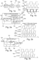
- Figure 1a illustrates a signal converter device 100 according to an exemplary embodiment of the present disclosure.
- the signal converter device 100 is configured for converting a single-ended input signal 105 into a differential signal 125.
- the device 100 comprises a multiplier device 110, configured to receive the single-ended incoming signal 105, and to multiply the incoming signal 105 by two to provide a multiplied signal 115.
- the device 100 further comprises a divider device 120 downstream of the multiplier device 110, and configured to receive the multiplied signal 115 from the multiplier device 110, and divide the multiplied signal 115 by two to provide the differential signal 125.
- the differential signal 125 comprises hereby two complementary phases 125a, 125b.
- Figure 1b illustrates examples of the signals that correspond to the above described signal converter device 100.
- the multiplied signal 115 (CLK) is double with respect to the incoming signal 105 (IN), while the differential signal 125 is again half of the multiplied signal 115. It can be seen that the two complementary phases 125a, 125b (OUT-P and OUT-N) of the differential signal 125 show perfect zero-crossing properties (see added circles).
- Figure 2a illustrates a signal converter device 100 as described for Figure 1a above, but in more detail according to an exemplary embodiment of the present disclosure.
- the divider device 120 is implemented as a differential symmetrical flip-flop device.
- FIG 2b illustrates examples of the signals that correspond to the above described signal converter device 100.
- the differential signal 125 shows perfect zero-crossing properties.
- the delayed input signal clkd is described below.
- the rising edges of the multiplied signal 115 (clkx2) are built with the input signal 105 (clk), which provides a more efficient noise suppression.
- only the rising edge is built with the input signal 105, while the falling edge is built with the delayed signal 106.
- the rising edge is important for noise suppression because the divider 120 is clocked on the rising edge of the multiplied signal 115.
- Each edge of the divider by two outputs (differential signal 125) is built with a rising edge of the multiplied signal 115 (clkx2).
- FIG 3a illustrates a multiplier device 110 according to an exemplary embodiment of the present disclosure.
- the multiplier device 110 comprises a delay-circuit that provides a delayed incoming signal 106 with respect to the incoming signal 105.
- the incoming signal 105 as well as the delayed incoming signal 106, are taken into account.
- an OR-gate 108 wherein the input to the OR-gate 108 comprises the incoming signal 105 and the delayed incoming signal 106.
- the output of the OR-gate 108 comprises the multiplied signal 115.
- the accuracy of the delay t is not important in this example. It only defines the accuracy of the falling edge of the clock signal (clk), while the divider device 120 is positive edge triggered (or vice versa).
- Figure 3b illustrates examples of the signals that correspond to the above described multiplier device 110.
- Figure 4a illustrates a signal converter device 100 with a synchronization device 130 according to an exemplary embodiment of the present disclosure.
- the synchronizer device 130 is configured to provide a plurality of synchronization signals 132a, 132b based on an incoming preset signal 131.
- the synchronization device 130 determines a difference between the incoming signal 105 and the preset signal 131 and provides, based on the result, a first synchronization signal 132a to the differential signal 125, and a second synchronization signal 132b to the multiplied signal 115.
- first synchronization signal 132a this is divided into two further first synchronization signals 133a,b each of which is applied to synchronize one of the complementary phases 125a, 125b of the differential signal 125.
- the second synchronization signal 132b is compared/combined with the multiplied signal 115 at a combiner device, e.g. an AND-gate (135), to provide a synchronized multiplied signal 116.
- the preset release of divider device 120 is synchronized to the input clock by a third synchronization signal 133c.
- Figure 4b illustrates the signal of the above described signal converter device 100 with the synchronizer device 130. Based on the preset synchronization signal 131, the synchronized multiplied signal 116 and the synchronized differential signal phases 125a, b will be truncated at an initial signal sequences.
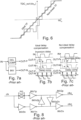
- Figure 5a illustrates a basic implementation of the divider device 120 using a differential symmetrical flip-flop circuit according to an exemplary embodiment of the present disclosure.
- Figure 5b illustrates a more detailed implementation of the divider device 120 with a synchronizer device 130 according to an exemplary embodiment of the present disclosure.
- an example at transistor level based on a sense-amplifier-based D-flip-flop which is differential and perfectly symmetrical.
- the synchronized preset signal 133c is applied to the left upper-most transistor (see circle).
- a pull-down nMOS forces the internal node A to the logic level low and the outputs QP to the logic level high.
- the right lower-most pMOS (see circle) is off, thereby ensuring that the node A can go to logic level low reliably.
- the logic level high on QP naturally forced a logic level low on QN (and a logic level high on internal node B).
- the right upper-most transistor (see circle) is optional for the preset functionality, but is used to ensure a complete symmetric design (the pMOS is always active, the nMOS is always off).
- Figure 6 illustrates the transfer function of a TDC (the phase difference of its two incoming signals is digitized) in an ideal situation (linear behavior) and in a real case, when non-idealities in the circuit cause non-linearities in the transfer function. Ensuring a highly stable zero-crossing (see also Figure 7b ) provides a transfer function that is more linear.
Landscapes
- Engineering & Computer Science (AREA)
- Theoretical Computer Science (AREA)
- Physics & Mathematics (AREA)
- General Engineering & Computer Science (AREA)
- General Physics & Mathematics (AREA)
- Computer Hardware Design (AREA)
- Nonlinear Science (AREA)
- Computing Systems (AREA)
- Mathematical Physics (AREA)
- Manipulation Of Pulses (AREA)
Abstract
Description
- The present disclosure relates to a signal converter device for converting a single-ended signal to a differential signal. Further, the present disclosure relates to a method of converting a single-ended signal to a differential signal. Thus, the present disclosure may refer to the technical field of signal conversion and signal processing.
- A signal converter is a device that is configured to convert a first signal into a second signal, being different from the first signal. For example, a signal converter can be configured to convert a single-ended signal into a differential signal.
- A Time to Digital Converter (TDC) is a device that quantifies the phase difference between an incoming signal S(t) and a reference signal Ref(t). In most of applications both, S(t) and Ref(t), are single-ended signals. Nevertheless, a differential incoming signal can permit an improved TDC performance in term of linearity and resolution. Many TDC implementations rely on a single-ended to differential signal converter to convert the single-ended incoming (CMOS) clock signal to a differential signal. However, such a single-ended to differential converter can again become a bottleneck for the TDC performance, due to a potentially low linearity and accordingly low Zero-Crossing (ZC) stability (ZC properties) of the single-ended to differential converter.
- Due to non-idealities of the design (and especially due to non-stable ZC properties), the transfer function (TF) of the TDC can be non-linear, lowering or degrading the PLL or system performances in which the TDC is used (see
Figure 6 ). - Conventionally, the complementary phases of the differential signal are generated by inverting the incoming single-ended signal. The delay introduced by the inverting circuit is then compensated to guarantee stable ZC properties between the differential phases. Even though many different delay compensation techniques have been described, the compensation has not been ideal, leading to inaccurate ZC properties of the differential signal.
-
Figure 7a shows a conventional example, wherein the complementary phases of the differential signal are generated by inverting the input signal and compensating for the inversion delay. However, if the delay compensation is not ideal, the zero crossings of the differential signal are modulated. In case of ideal delay compensation, the zero crossing are equally spaced, with period TZC (seeFigure 7b ). In case of not ideal compensation (which occurs for the conventional example), the zero crossing properties are not equally time spaced (TZC1 ≠ TZC2), as can be seen inFigure 7c . -
Figure 8 shows a conventional approach in more detail, wherein differential signals are generated rail-to-rail. Inverters are coupled in series, and the opposite signal phase is built by inverting the input with an additional inverter (INV0n). Since the two paths are not symmetrical, a stable differential output ZC at half of the supply voltage is difficult to obtain. To stabilize the output ZC, it is further required to fine-tune the components of each path. A pass-gate (PG) can be used in series in the path lacking one inverter to balance the signals propagation speed. Further, in this example, additional resynchronization inverters INVp2n and INVn2p are used to force the two paths to work in phase opposition. Nevertheless, non-symmetries remain and the ZC properties of the differential outputs are still sensitive to process and mismatches. - There may be a need to convert a single-ended signal to a differential signal in an efficient and robust manner, in particular with highly stable zero-crossing properties. A device and a method according to the independent claims are described in the following. Exemplary embodiments are described by the dependent claims.
- According to an aspect of the present disclosure, there is described a signal converter device (for example being configured as or being part of a time-to-digital converter) for converting a single-ended signal (e.g. a clock signal) to a differential signal, the device comprising:
- i) a (frequency) multiplier device (e.g. a multiplier circuit), configured to ia) receive a single-ended incoming signal, and
- ib) multiply the incoming signal (frequency) (in particular by two) to provide a multiplied signal (frequency) (i.e. a signal whose frequency is multiplied); and
- ii) a (frequency) divider device (in particular a differential device, more in particular a fully symmetrical differential device), configured to
- iia) receive the multiplied signal, and
- iib) divide the multiplied signal (in particular by two) to provide a differential signal (a differential signal comprises two complementary signal phases). In particular, the factor of the multiplication and the division is the same, more in particular two.
- According to an aspect of the present disclosure, there is described a method of converting a single-ended signal to a differential signal, the method comprising:
- i) receiving a single-ended incoming signal;
- ii) multiplying the incoming signal (frequency) to provide a multiplied signal (frequency); and subsequently
- iii) dividing the multiplied signal to provide a differential signal.
- According to an exemplary embodiment of the present disclosure, a single-ended signal may be converted to a differential signal in an efficient and robust manner (in particular with a highly stable zero-crossing output), when the single-ended input signal frequency is multiplied and subsequently divided (in particular based on a symmetrical system) to provide a differential output signal. This approach may overcome limitations of the prior art by having an optimized symmetry of the path that generates the differential signal(s). In particular, there may be no need to invert any signal or to compensate any delay, because the differential signal generation with high ZC precision may be guaranteed by the signal converter design (in particular the ideal symmetrical structure).
- Conventionally, several tricks are applied in order to compensate for consequences of non-symmetries of a single-to-differential converter (see also discussion further above). In contrast to these complex and error-prone approaches, it is described here for the first time a simple and easy-to-implement approach that is at the same time a true symmetrical design that reliably provides differential signals with a highly stable zero-crossing output.
- The described approach may be efficiently applied in different electronic applications that relate to signal conversion. In particular, the linearity of a time-to-digital converter may be significantly improved.
- In the following, further exemplary embodiments of the device and the method will be explained.
- According to an embodiment, the multiplier device is configured to multiply by two and/or a multiple of two (the input signal frequency). In the present context, the term multiplier device may refer to any circuit that is configured to multiply an incoming (clock) signal (frequency). The term multiple of two may refer to a product of the number two and a further natural number. Thus, the multiple of two may be for example be four, six, eight, etc.
- According to a further embodiment, the divider device is configured to divide by two and/or the multiple of two. In the present context, the term divider device may refer to any circuit that is configured to divide an incoming (clock) signal and thereby providing a differential signal. In an example, a divider device may be a symmetrical differential device. In a further example, the number of multiplication and division is the same.
- According to a further embodiment, at least one of the incoming signal, the multiplied signal, and the differential signal is a clock signal.
- According to a further embodiment, the multiplication is a frequency multiplication. According to a further embodiment, the division is a frequency division. In particular, the frequency of the single ended incoming signal and the differential output signal is the same.
- According to a further embodiment, the multiplier device is further configured to provide a delayed incoming signal of the incoming signal, and include the delayed incoming signal in the multiplication. Thereby, a reliable multiplication operation may be established.
- According to a further embodiment, the multiplier device further comprises an XOR-gate, wherein the input to the XOR-gate comprises the incoming signal and the delayed incoming signal, and wherein the output of the XOR-gate comprises the multiplied signal.
- According to a further embodiment, the divider device comprises a differential flip-flop circuit, in particular a differential symmetrical flip-flop circuit. In this manner, the implementation may be straightforward using tested and established devices. The symmetrical design may in particular lead to a highly stable ZC output.
- According to a further embodiment, the device is at least partially configured in CMOS. Thereby, the described concept may be implemented in an established and robust environment.
- According to a further embodiment, the signal converter device further comprises a synchronizer device (in particular coupled between the multiplier device and the divider device), and configured to i) provide a preset signal, and ii) synchronize at least one of the multiplied signal and the differential signal with respect to the preset signal. In an example, if no care is applied, the initial phase of some symmetrical divider implementation is unknow (it depends on the mismatch of some divider components). Hereby, implementing a preset function that forces the initial state of the divider outputs can solve this issue.
- According to a further embodiment, the device further comprises a combiner (e.g. an , AND-gate), coupled in between the multiplier device and the divider device, wherein the synchronizer device is configured to provide a synchronization signal to the combiner to generate a synchronized multiplied signal. This implementation may be efficient to couple the preset signal into the multiplier-divider path.
- According to a further embodiment, there is provided a time-to-digital converter that comprises the device as described above. By achieving a highly stable ZC output, linearity of the TDC may be improved.
-
-
Figure 1a illustrates a signal converter device andFigure 1b illustrates the corresponding signals according to an exemplary embodiment of the present disclosure. -
Figure 2a illustrates a signal converter device in more detail andFigure 2b illustrates the corresponding signals according to an exemplary embodiment of the present disclosure. -
Figure 3a illustrates a multiplier device andFigure 3b illustrates the corresponding signals according to an exemplary embodiment of the present disclosure. -
Figure 4a illustrates a signal converter device with a synchronization device andFigure 4b illustrates the corresponding signals according to an exemplary embodiment of the present disclosure. -
Figure 5a illustrates a basic implementation of the divider device, whileFigure 5b illustrates a more detailed implementation of the divider device on transistor level according to an exemplary embodiment of the present disclosure. -
Figure 6 illustrates a highly stable zero-crossing output according to an exemplary embodiment of the present disclosure in comparison with a conventional output. -
Figures 7a and 7c illustrate a prior art conversion device with the corresponding signals, whileFigure 7b illustrates the signals of a signal conversion device according to an exemplary embodiment of the present disclosure. -
Figure 8 illustrates a conventional approach for signal conversion. - Before referring to the drawings, exemplary embodiments will be described in further detail, some basic considerations will be summarized based on which exemplary embodiments of the present disclosure have been developed.
- According to an exemplary embodiment of the present disclosure, there is generated a differential signal by a fully differential sense-amplifier-based D-flip-flop which is used as a frequency divider by two. It requires then in-front a frequency multiplier by two, that receives the single-ended input signal, and provides a clock signal multiplied by two. Since the proposed approach does not rely on an inversion to generate the complementary phase, there is no additional delay which would have to be compensated. Thereby, the accuracy of a differential signal ZC precision is guaranteed by construction.
- According to an exemplary embodiment of the present disclosure, there is described the usage of a differential frequency divider by two (e.g a differential flip-flop) with a frequency multiplier by two in front. A single-ended signal goes to the frequency multiplier by two, and the multiplier output signal is fed to a fully-differential frequency divider by two. The output of the fully differential divider is a differential signal at the same frequency as the original single-ended signal. Due to the fully differential implementation of the divider device, the two differential signal phases are exactly 180 degrees apart.
- According to an exemplary embodiment of the present disclosure, a differential CMOS clock is generated by frequency multiplying by two the single-ended input signal, while the multiplied by two signal is then used as a clock for a differential (symmetrical) divide by two circuit. The output of the divider by two is the desired differential signal, which is differential by construction.
-
Figure 1a illustrates asignal converter device 100 according to an exemplary embodiment of the present disclosure. Thesignal converter device 100 is configured for converting a single-endedinput signal 105 into adifferential signal 125. Thedevice 100 comprises amultiplier device 110, configured to receive the single-endedincoming signal 105, and to multiply theincoming signal 105 by two to provide a multipliedsignal 115. Thedevice 100 further comprises adivider device 120 downstream of themultiplier device 110, and configured to receive the multipliedsignal 115 from themultiplier device 110, and divide the multipliedsignal 115 by two to provide thedifferential signal 125. Thedifferential signal 125 comprises hereby twocomplementary phases -
Figure 1b illustrates examples of the signals that correspond to the above describedsignal converter device 100. The multiplied signal 115 (CLK) is double with respect to the incoming signal 105 (IN), while thedifferential signal 125 is again half of the multipliedsignal 115. It can be seen that the twocomplementary phases differential signal 125 show perfect zero-crossing properties (see added circles). -
Figure 2a illustrates asignal converter device 100 as described forFigure 1a above, but in more detail according to an exemplary embodiment of the present disclosure. In this example, thedivider device 120 is implemented as a differential symmetrical flip-flop device. -
Figure 2b illustrates examples of the signals that correspond to the above describedsignal converter device 100. Like in the case ofFigure 1b , thedifferential signal 125 shows perfect zero-crossing properties. The delayed input signal clkd is described below. The rising edges of the multiplied signal 115 (clkx2) are built with the input signal 105 (clk), which provides a more efficient noise suppression. In this example, only the rising edge is built with theinput signal 105, while the falling edge is built with the delayedsignal 106. Hereby, only the rising edge is important for noise suppression because thedivider 120 is clocked on the rising edge of the multipliedsignal 115. Each edge of the divider by two outputs (differential signal 125) is built with a rising edge of the multiplied signal 115 (clkx2). -
Figure 3a illustrates amultiplier device 110 according to an exemplary embodiment of the present disclosure. Themultiplier device 110 comprises a delay-circuit that provides a delayedincoming signal 106 with respect to theincoming signal 105. When performing the multiplication, theincoming signal 105, as well as the delayedincoming signal 106, are taken into account. Specifically, in this example, there is provided an OR-gate 108, wherein the input to theOR-gate 108 comprises theincoming signal 105 and the delayedincoming signal 106. As a consequence, the output of theOR-gate 108 comprises the multipliedsignal 115. The accuracy of the delay t is not important in this example. It only defines the accuracy of the falling edge of the clock signal (clk), while thedivider device 120 is positive edge triggered (or vice versa). -
Figure 3b illustrates examples of the signals that correspond to the above describedmultiplier device 110. -
Figure 4a illustrates asignal converter device 100 with asynchronization device 130 according to an exemplary embodiment of the present disclosure. Thesynchronizer device 130 is configured to provide a plurality ofsynchronization signals preset signal 131. Thesynchronization device 130 determines a difference between theincoming signal 105 and thepreset signal 131 and provides, based on the result, afirst synchronization signal 132a to thedifferential signal 125, and asecond synchronization signal 132b to the multipliedsignal 115. Regarding thefirst synchronization signal 132a, this is divided into two furtherfirst synchronization signals 133a,b each of which is applied to synchronize one of thecomplementary phases differential signal 125. Thesecond synchronization signal 132b is compared/combined with the multipliedsignal 115 at a combiner device, e.g. an AND-gate (135), to provide a synchronized multipliedsignal 116. - The preset release of
divider device 120 is synchronized to the input clock by athird synchronization signal 133c. -
Figure 4b illustrates the signal of the above describedsignal converter device 100 with thesynchronizer device 130. Based on thepreset synchronization signal 131, the synchronized multipliedsignal 116 and the synchronizeddifferential signal phases 125a, b will be truncated at an initial signal sequences. -
Figure 5a illustrates a basic implementation of thedivider device 120 using a differential symmetrical flip-flop circuit according to an exemplary embodiment of the present disclosure. -
Figure 5b illustrates a more detailed implementation of thedivider device 120 with asynchronizer device 130 according to an exemplary embodiment of the present disclosure. Specifically, there is shown an example at transistor level based on a sense-amplifier-based D-flip-flop, which is differential and perfectly symmetrical. The synchronizedpreset signal 133c is applied to the left upper-most transistor (see circle). Then, a pull-down nMOS forces the internal node A to the logic level low and the outputs QP to the logic level high. The right lower-most pMOS (see circle) is off, thereby ensuring that the node A can go to logic level low reliably. The logic level high on QP naturally forced a logic level low on QN (and a logic level high on internal node B). The right upper-most transistor (see circle) is optional for the preset functionality, but is used to ensure a complete symmetric design (the pMOS is always active, the nMOS is always off). -
Figure 6 illustrates the transfer function of a TDC (the phase difference of its two incoming signals is digitized) in an ideal situation (linear behavior) and in a real case, when non-idealities in the circuit cause non-linearities in the transfer function. Ensuring a highly stable zero-crossing (see alsoFigure 7b ) provides a transfer function that is more linear. -
- 100
- Signal converter device
- 105
- Incoming single-ended signal
- 106
- Delayed incoming signal
- 108
- XOR-gate
- 110
- Multiplier device
- 115
- Multiplied signal
- 116
- Synchronized multiplied signal
- 120
- Divider device
- 125
- Divided differential signal
- 125a,b
- Divided differential signals
- 130
- Synchronization device
- 131
- Preset signal
- 132a
- First synchronization signal for differential signal
- 132b
- Second synchronization signal for multiplied signal
- 133a,b,c
- Further synchronization signals
- 135
- Combiner, AND-gate
Claims (15)
- A signal converter device (100) for converting a single-ended signal to a differential signal, the device (100) comprising:a multiplier device (110), configured toreceive a single-ended incoming signal (105), andmultiply the incoming signal (105) to provide a multiplied signal (115); anda divider device (120), configured toreceive the multiplied signal (115), anddivide the multiplied signal (115) to provide a differential signal (125a, 125b).
- The signal converter device (100) according to claim 1,
wherein the multiplier device (110) is configured to multiply by two or a multiple of two. - The signal converter device (100) according to claim 1 or 2,
wherein the divider device (120) is configured to divide by two or the multiple of two. - The signal converter device (100) according to any one of the preceding claims, wherein at least one of the incoming signal (105) and the multiplied signal (115) is a clock signal.
- The signal converter device (100) according to any one of the preceding claims, comprising at least one of the following features:wherein the multiplication is a frequency multiplication;wherein the division is a frequency division.
- The signal converter device (100) according to any one of the preceding claims, wherein the multiplier device (110) is further configured toprovide a delayed incoming signal (106) of the incoming signal (105), andinclude a delayed incoming signal (106) in the multiplication.
- The signal converter device (100) according to claim 6,wherein the multiplier device (110) further comprises an XOR-gate (108),wherein the input to the XOR-gate (108) comprises the incoming signal (105) and the delayed incoming signal (106), andwherein the output of the XOR-gate (108) comprises the multiplied signal (115).
- The signal converter device (100) according to any one of the preceding claims, wherein the divider device (120) comprises a differential flip-flop circuit.
- The signal converter device (100) according to claim 8, wherein the differential flip-flop circuit is configured as a symmetrical differential flip-flop circuit.
- The signal converter device (100) according to any one of the preceding claims, wherein the device (100) is at least partially configured in CMOS.
- The signal converter device (100) according to any one of the preceding claims, further comprising:
a synchronizer device (130) configured toprovide a preset signal (132a, 132b), andsynchronize at least one of the multiplied signal (115) and the differential signal (125) with respect to the preset signal (131). - The signal converter device (100) according to claim 11, further comprising:
a combiner, coupled in between the multiplier device (110) and the divider device (120);
wherein the synchronizer device (130) is configured to provide a synchronization signal (132b) to the combiner (135) to generate a synchronized multiplied signal (116). - The signal converter device (100) according to claim 12,
wherein the combiner comprises or consists of an AND-gate (135). - A time-to-digital converter that comprises the device (100) according to any one of the preceding claims.
- A method of converting a single-ended signal to a differential signal, the method comprising:receiving a single-ended incoming signal (105);multiplying the incoming signal (105) to provide a multiplied signal (115); and subsequentlydividing the multiplied signal (115) to provide a differential signal (125a, 125b).
Priority Applications (3)
| Application Number | Priority Date | Filing Date | Title |
|---|---|---|---|
| EP22305105.3A EP4220959A1 (en) | 2022-01-31 | 2022-01-31 | Single-ended to differential signal converter, and signal converting method |
| US18/061,674 US11979157B2 (en) | 2022-01-31 | 2022-12-05 | Single-ended to differential signal converter, and signal converting method |
| CN202310026127.XA CN116521590A (en) | 2022-01-31 | 2023-01-09 | Single-ended to differential signal converter and signal conversion method |
Applications Claiming Priority (1)
| Application Number | Priority Date | Filing Date | Title |
|---|---|---|---|
| EP22305105.3A EP4220959A1 (en) | 2022-01-31 | 2022-01-31 | Single-ended to differential signal converter, and signal converting method |
Publications (1)
| Publication Number | Publication Date |
|---|---|
| EP4220959A1 true EP4220959A1 (en) | 2023-08-02 |
Family
ID=80623601
Family Applications (1)
| Application Number | Title | Priority Date | Filing Date |
|---|---|---|---|
| EP22305105.3A Pending EP4220959A1 (en) | 2022-01-31 | 2022-01-31 | Single-ended to differential signal converter, and signal converting method |
Country Status (3)
| Country | Link |
|---|---|
| US (1) | US11979157B2 (en) |
| EP (1) | EP4220959A1 (en) |
| CN (1) | CN116521590A (en) |
Citations (1)
| Publication number | Priority date | Publication date | Assignee | Title |
|---|---|---|---|---|
| CN113726335A (en) * | 2021-08-24 | 2021-11-30 | 平头哥(上海)半导体技术有限公司 | Clock control circuit, clock circuit, and electronic device |
Family Cites Families (5)
| Publication number | Priority date | Publication date | Assignee | Title |
|---|---|---|---|---|
| KR100247912B1 (en) * | 1993-02-23 | 2000-03-15 | 윤종용 | Frequency multiplication circuit |
| US6433595B1 (en) * | 2001-09-05 | 2002-08-13 | Qantec Communication, Inc. | Method of system circuit design and circuitry for high speed data communication |
| US6686787B2 (en) * | 2002-02-28 | 2004-02-03 | Kuok Ling | High-speed fully balanced differential flip-flop with reset |
| JP5471427B2 (en) | 2009-12-25 | 2014-04-16 | 富士通株式会社 | Single-phase differential conversion circuit |
| US10972057B2 (en) | 2016-12-20 | 2021-04-06 | Sony Semiconductor Solutions Corporation | Single-phase differential conversion circuit, signal processing method for use therewith, and reception apparatus |
-
2022
- 2022-01-31 EP EP22305105.3A patent/EP4220959A1/en active Pending
- 2022-12-05 US US18/061,674 patent/US11979157B2/en active Active
-
2023
- 2023-01-09 CN CN202310026127.XA patent/CN116521590A/en active Pending
Patent Citations (1)
| Publication number | Priority date | Publication date | Assignee | Title |
|---|---|---|---|---|
| CN113726335A (en) * | 2021-08-24 | 2021-11-30 | 平头哥(上海)半导体技术有限公司 | Clock control circuit, clock circuit, and electronic device |
Non-Patent Citations (1)
| Title |
|---|
| WELP BENEDIKT ET AL: "A 1-30 GHz 3-bit vector modulator based on ultra-wideband IQ-generation for MIMO-radar-systems in SiGe BiCMOS", 2017 IEEE RADIO FREQUENCY INTEGRATED CIRCUITS SYMPOSIUM (RFIC), IEEE, 4 June 2017 (2017-06-04), pages 300 - 303, XP033115807, DOI: 10.1109/RFIC.2017.7969077 * |
Also Published As
| Publication number | Publication date |
|---|---|
| US20230246635A1 (en) | 2023-08-03 |
| US11979157B2 (en) | 2024-05-07 |
| CN116521590A (en) | 2023-08-01 |
Similar Documents
| Publication | Publication Date | Title |
|---|---|---|
| JP3945874B2 (en) | Method for synchronizing signals and structure therefor | |
| US9503115B1 (en) | Circuit for and method of implementing a time-interleaved analog-to-digital converter | |
| US8471607B1 (en) | High-speed frequency divider architecture | |
| US7576584B2 (en) | Clock generators for generation of in-phase and quadrature clock signals | |
| US10886930B1 (en) | Voltage controlled oscillator based analog-to-digital converter including a maximum length sequence generator | |
| US5230013A (en) | PLL-based precision phase shifting at CMOS levels | |
| US7034595B2 (en) | Multi-phase clock signal generators and methods of generating multi-phase clock signals | |
| KR102402879B1 (en) | High speed low power digital to analog upconverter | |
| US12249996B2 (en) | Counter design for a time-to-digital converter (TDC) | |
| EP4049369A1 (en) | Quadrature clock skew calibration circuit | |
| US9331705B2 (en) | Timing adjustment circuit, clock generation circuit, and method for timing adjustment | |
| US11979157B2 (en) | Single-ended to differential signal converter, and signal converting method | |
| US11843388B2 (en) | Can transmitter | |
| US11356112B1 (en) | Coarse-fine counting architecture for a VCO-ADC based on interlocked binary asynchronous counters | |
| US7378885B1 (en) | Multiphase divider for P-PLL based serial link receivers | |
| CN114675525B (en) | Time-to-digital converter and clock synchronization system | |
| US12525964B2 (en) | Three-stage differential ring oscillator generating differential in-phase and quadrature-phase clocks | |
| US8355478B1 (en) | Circuit for aligning clock to parallel data | |
| CN115425954A (en) | Multi-phase clock signal generating circuit | |
| KR20230169726A (en) | Phase blender circuit and multi-phase clock signal correction circuit including the same | |
| Tsimpos et al. | Multi-rate phase interpolator for high speed serial interfaces | |
| US20240283630A1 (en) | Digital quadrature clock for low jitter applications | |
| EP4037190A1 (en) | System and method for generating subharmonic locked frequency division and phase interpolation | |
| US5204885A (en) | Method and device for evaluating a digital signal using a digital counter with lsb signal separately applied to both counter and register | |
| Liu et al. | A New Multilevel Interpolated TDC Method Based on a Two-Step Synchronizer |
Legal Events
| Date | Code | Title | Description |
|---|---|---|---|
| PUAI | Public reference made under article 153(3) epc to a published international application that has entered the european phase |
Free format text: ORIGINAL CODE: 0009012 |
|
| STAA | Information on the status of an ep patent application or granted ep patent |
Free format text: STATUS: THE APPLICATION HAS BEEN PUBLISHED |
|
| AK | Designated contracting states |
Kind code of ref document: A1 Designated state(s): AL AT BE BG CH CY CZ DE DK EE ES FI FR GB GR HR HU IE IS IT LI LT LU LV MC MK MT NL NO PL PT RO RS SE SI SK SM TR |
|
| STAA | Information on the status of an ep patent application or granted ep patent |
Free format text: STATUS: REQUEST FOR EXAMINATION WAS MADE |
|
| 17P | Request for examination filed |
Effective date: 20240202 |
|
| RBV | Designated contracting states (corrected) |
Designated state(s): AL AT BE BG CH CY CZ DE DK EE ES FI FR GB GR HR HU IE IS IT LI LT LU LV MC MK MT NL NO PL PT RO RS SE SI SK SM TR |