EP4220922A2 - Method for controlling power conversion device and power conversion device - Google Patents
Method for controlling power conversion device and power conversion device Download PDFInfo
- Publication number
- EP4220922A2 EP4220922A2 EP23180004.6A EP23180004A EP4220922A2 EP 4220922 A2 EP4220922 A2 EP 4220922A2 EP 23180004 A EP23180004 A EP 23180004A EP 4220922 A2 EP4220922 A2 EP 4220922A2
- Authority
- EP
- European Patent Office
- Prior art keywords
- impedance
- rectifier
- conversion device
- power conversion
- input
- Prior art date
- Legal status (The legal status is an assumption and is not a legal conclusion. Google has not performed a legal analysis and makes no representation as to the accuracy of the status listed.)
- Granted
Links
Images


Classifications
-
- H—ELECTRICITY
- H02—GENERATION; CONVERSION OR DISTRIBUTION OF ELECTRIC POWER
- H02M—APPARATUS FOR CONVERSION BETWEEN AC AND AC, BETWEEN AC AND DC, OR BETWEEN DC AND DC, AND FOR USE WITH MAINS OR SIMILAR POWER SUPPLY SYSTEMS; CONVERSION OF DC OR AC INPUT POWER INTO SURGE OUTPUT POWER; CONTROL OR REGULATION THEREOF
- H02M3/00—Conversion of DC power input into DC power output
- H02M3/22—Conversion of DC power input into DC power output with intermediate conversion into AC
- H02M3/24—Conversion of DC power input into DC power output with intermediate conversion into AC by static converters
- H02M3/28—Conversion of DC power input into DC power output with intermediate conversion into AC by static converters using discharge tubes with control electrode or semiconductor devices with control electrode to produce the intermediate AC
- H02M3/325—Conversion of DC power input into DC power output with intermediate conversion into AC by static converters using discharge tubes with control electrode or semiconductor devices with control electrode to produce the intermediate AC using devices of a triode or a transistor type requiring continuous application of a control signal
- H02M3/335—Conversion of DC power input into DC power output with intermediate conversion into AC by static converters using discharge tubes with control electrode or semiconductor devices with control electrode to produce the intermediate AC using devices of a triode or a transistor type requiring continuous application of a control signal using semiconductor devices only
- H02M3/33569—Conversion of DC power input into DC power output with intermediate conversion into AC by static converters using discharge tubes with control electrode or semiconductor devices with control electrode to produce the intermediate AC using devices of a triode or a transistor type requiring continuous application of a control signal using semiconductor devices only having several active switching elements
-
- H—ELECTRICITY
- H02—GENERATION; CONVERSION OR DISTRIBUTION OF ELECTRIC POWER
- H02M—APPARATUS FOR CONVERSION BETWEEN AC AND AC, BETWEEN AC AND DC, OR BETWEEN DC AND DC, AND FOR USE WITH MAINS OR SIMILAR POWER SUPPLY SYSTEMS; CONVERSION OF DC OR AC INPUT POWER INTO SURGE OUTPUT POWER; CONTROL OR REGULATION THEREOF
- H02M3/00—Conversion of DC power input into DC power output
- H02M3/02—Conversion of DC power input into DC power output without intermediate conversion into AC
- H02M3/04—Conversion of DC power input into DC power output without intermediate conversion into AC by static converters
- H02M3/10—Conversion of DC power input into DC power output without intermediate conversion into AC by static converters using discharge tubes with control electrode or semiconductor devices with control electrode
- H02M3/145—Conversion of DC power input into DC power output without intermediate conversion into AC by static converters using discharge tubes with control electrode or semiconductor devices with control electrode using devices of a triode or transistor type requiring continuous application of a control signal
- H02M3/155—Conversion of DC power input into DC power output without intermediate conversion into AC by static converters using discharge tubes with control electrode or semiconductor devices with control electrode using devices of a triode or transistor type requiring continuous application of a control signal using semiconductor devices only
- H02M3/156—Conversion of DC power input into DC power output without intermediate conversion into AC by static converters using discharge tubes with control electrode or semiconductor devices with control electrode using devices of a triode or transistor type requiring continuous application of a control signal using semiconductor devices only with automatic control of output voltage or current, e.g. switching regulators
-
- H—ELECTRICITY
- H02—GENERATION; CONVERSION OR DISTRIBUTION OF ELECTRIC POWER
- H02M—APPARATUS FOR CONVERSION BETWEEN AC AND AC, BETWEEN AC AND DC, OR BETWEEN DC AND DC, AND FOR USE WITH MAINS OR SIMILAR POWER SUPPLY SYSTEMS; CONVERSION OF DC OR AC INPUT POWER INTO SURGE OUTPUT POWER; CONTROL OR REGULATION THEREOF
- H02M1/00—Details of apparatus for conversion
- H02M1/0048—Circuits or arrangements for reducing losses
- H02M1/0054—Transistor switching losses
- H02M1/0058—Transistor switching losses by employing soft switching techniques, i.e. commutation of transistors when applied voltage is zero or when current flow is zero
-
- H—ELECTRICITY
- H02—GENERATION; CONVERSION OR DISTRIBUTION OF ELECTRIC POWER
- H02M—APPARATUS FOR CONVERSION BETWEEN AC AND AC, BETWEEN AC AND DC, OR BETWEEN DC AND DC, AND FOR USE WITH MAINS OR SIMILAR POWER SUPPLY SYSTEMS; CONVERSION OF DC OR AC INPUT POWER INTO SURGE OUTPUT POWER; CONTROL OR REGULATION THEREOF
- H02M1/00—Details of apparatus for conversion
- H02M1/32—Means for protecting converters other than automatic disconnection
-
- H—ELECTRICITY
- H02—GENERATION; CONVERSION OR DISTRIBUTION OF ELECTRIC POWER
- H02M—APPARATUS FOR CONVERSION BETWEEN AC AND AC, BETWEEN AC AND DC, OR BETWEEN DC AND DC, AND FOR USE WITH MAINS OR SIMILAR POWER SUPPLY SYSTEMS; CONVERSION OF DC OR AC INPUT POWER INTO SURGE OUTPUT POWER; CONTROL OR REGULATION THEREOF
- H02M1/00—Details of apparatus for conversion
- H02M1/32—Means for protecting converters other than automatic disconnection
- H02M1/327—Means for protecting converters other than automatic disconnection against abnormal temperatures
-
- H—ELECTRICITY
- H02—GENERATION; CONVERSION OR DISTRIBUTION OF ELECTRIC POWER
- H02M—APPARATUS FOR CONVERSION BETWEEN AC AND AC, BETWEEN AC AND DC, OR BETWEEN DC AND DC, AND FOR USE WITH MAINS OR SIMILAR POWER SUPPLY SYSTEMS; CONVERSION OF DC OR AC INPUT POWER INTO SURGE OUTPUT POWER; CONTROL OR REGULATION THEREOF
- H02M3/00—Conversion of DC power input into DC power output
- H02M3/01—Resonant DC/DC converters
-
- H—ELECTRICITY
- H02—GENERATION; CONVERSION OR DISTRIBUTION OF ELECTRIC POWER
- H02M—APPARATUS FOR CONVERSION BETWEEN AC AND AC, BETWEEN AC AND DC, OR BETWEEN DC AND DC, AND FOR USE WITH MAINS OR SIMILAR POWER SUPPLY SYSTEMS; CONVERSION OF DC OR AC INPUT POWER INTO SURGE OUTPUT POWER; CONTROL OR REGULATION THEREOF
- H02M3/00—Conversion of DC power input into DC power output
- H02M3/02—Conversion of DC power input into DC power output without intermediate conversion into AC
- H02M3/04—Conversion of DC power input into DC power output without intermediate conversion into AC by static converters
- H02M3/10—Conversion of DC power input into DC power output without intermediate conversion into AC by static converters using discharge tubes with control electrode or semiconductor devices with control electrode
- H02M3/145—Conversion of DC power input into DC power output without intermediate conversion into AC by static converters using discharge tubes with control electrode or semiconductor devices with control electrode using devices of a triode or transistor type requiring continuous application of a control signal
- H02M3/155—Conversion of DC power input into DC power output without intermediate conversion into AC by static converters using discharge tubes with control electrode or semiconductor devices with control electrode using devices of a triode or transistor type requiring continuous application of a control signal using semiconductor devices only
-
- H—ELECTRICITY
- H02—GENERATION; CONVERSION OR DISTRIBUTION OF ELECTRIC POWER
- H02M—APPARATUS FOR CONVERSION BETWEEN AC AND AC, BETWEEN AC AND DC, OR BETWEEN DC AND DC, AND FOR USE WITH MAINS OR SIMILAR POWER SUPPLY SYSTEMS; CONVERSION OF DC OR AC INPUT POWER INTO SURGE OUTPUT POWER; CONTROL OR REGULATION THEREOF
- H02M7/00—Conversion of AC power input into DC power output; Conversion of DC power input into AC power output
- H02M7/02—Conversion of AC power input into DC power output without possibility of reversal
- H02M7/04—Conversion of AC power input into DC power output without possibility of reversal by static converters
- H02M7/06—Conversion of AC power input into DC power output without possibility of reversal by static converters using discharge tubes without control electrode or semiconductor devices without control electrode
-
- H—ELECTRICITY
- H02—GENERATION; CONVERSION OR DISTRIBUTION OF ELECTRIC POWER
- H02M—APPARATUS FOR CONVERSION BETWEEN AC AND AC, BETWEEN AC AND DC, OR BETWEEN DC AND DC, AND FOR USE WITH MAINS OR SIMILAR POWER SUPPLY SYSTEMS; CONVERSION OF DC OR AC INPUT POWER INTO SURGE OUTPUT POWER; CONTROL OR REGULATION THEREOF
- H02M7/00—Conversion of AC power input into DC power output; Conversion of DC power input into AC power output
- H02M7/42—Conversion of DC power input into AC power output without possibility of reversal
- H02M7/44—Conversion of DC power input into AC power output without possibility of reversal by static converters
- H02M7/48—Conversion of DC power input into AC power output without possibility of reversal by static converters using discharge tubes with control electrode or semiconductor devices with control electrode
-
- H—ELECTRICITY
- H02—GENERATION; CONVERSION OR DISTRIBUTION OF ELECTRIC POWER
- H02M—APPARATUS FOR CONVERSION BETWEEN AC AND AC, BETWEEN AC AND DC, OR BETWEEN DC AND DC, AND FOR USE WITH MAINS OR SIMILAR POWER SUPPLY SYSTEMS; CONVERSION OF DC OR AC INPUT POWER INTO SURGE OUTPUT POWER; CONTROL OR REGULATION THEREOF
- H02M7/00—Conversion of AC power input into DC power output; Conversion of DC power input into AC power output
- H02M7/42—Conversion of DC power input into AC power output without possibility of reversal
- H02M7/44—Conversion of DC power input into AC power output without possibility of reversal by static converters
- H02M7/48—Conversion of DC power input into AC power output without possibility of reversal by static converters using discharge tubes with control electrode or semiconductor devices with control electrode
- H02M7/4815—Resonant converters
-
- Y—GENERAL TAGGING OF NEW TECHNOLOGICAL DEVELOPMENTS; GENERAL TAGGING OF CROSS-SECTIONAL TECHNOLOGIES SPANNING OVER SEVERAL SECTIONS OF THE IPC; TECHNICAL SUBJECTS COVERED BY FORMER USPC CROSS-REFERENCE ART COLLECTIONS [XRACs] AND DIGESTS
- Y02—TECHNOLOGIES OR APPLICATIONS FOR MITIGATION OR ADAPTATION AGAINST CLIMATE CHANGE
- Y02B—CLIMATE CHANGE MITIGATION TECHNOLOGIES RELATED TO BUILDINGS, e.g. HOUSING, HOUSE APPLIANCES OR RELATED END-USER APPLICATIONS
- Y02B70/00—Technologies for an efficient end-user side electric power management and consumption
- Y02B70/10—Technologies improving the efficiency by using switched-mode power supplies [SMPS], i.e. efficient power electronics conversion e.g. power factor correction or reduction of losses in power supplies or efficient standby modes
Definitions
- the present invention relates to a power conversion device including an alternating-current (AC) wave generation circuit for generating an AC wave and a rectifier circuit for rectifying the AC wave generated by the AC wave generation circuit with a configuration including a rectifier capacitor and a diode connected in parallel, and a method for controlling the power conversion device.
- AC alternating-current
- Circuits for rectifying an AC wave are known, such as a class-E rectifier circuit as disclosed in Patent Document 1.
- Patent Document 1 International Publication WO 2015/087396
- the capacitance value of the capacitor constituting the rectifier circuit changes depending on the temperature characteristics. For example, since the capacitance of the capacitor decreases as the temperature increases, a peak value of a voltage waveform subjected to half-wave rectification in the rectifier circuit increases in association with the decrease in the capacitance, leading to a decrease in impedance. After that, since the temperature of the capacitor rises further, the same phenomenon is repeated, and there is a problem that over temperature occurs beyond a rated temperature of components.
- the present invention provides a power conversion device capable of suppressing a change in impedance of a capacitor included in a rectifier circuit to prevent over temperature, and a method for controlling the power conversion device.
- an aspect of the present invention provides a power conversion device and a method for controlling the power conversion device configured to regulate an alternating-current wave input to a rectifier capacitor depending on a change in impedance of the rectifier capacitor so as to suppress the change in the impedance of the rectifier capacitor.
- the present invention can suppress a change in impedance of a rectifier capacitor included in a rectifier circuit to prevent over temperature in the rectifier capacitor.
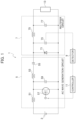
- Fig. 1 is a circuit diagram illustrating a configuration of a power conversion device according to the present embodiment.
- the power conversion device 1 includes an input power supply 3, an alternating-current (AC) wave generation circuit 5, a rectifier circuit 7, a detector 9, a controller 11, and a load 13.
- the power conversion device 1 converts direct current (DC) power input from the input power supply 3 into AC power, and supplies DC power rectified by the rectifier circuit 7 to the load 13.
- DC direct current
- the AC wave generation circuit 5 includes a choke coil 51, a resonant coil 53, a resonant capacitor 55, a switching element 57, and a shunt capacitor 59.
- the AC wave generation circuit 5 is a class-E inverter circuit that generates an AC wave from the DC power from the input power supply 3 depending on a drive frequency of the switching element 57.
- the choke coil 51 is connected between the input power supply 3 and the switching element 57.
- the resonant coil 53 and the resonant capacitor 55 form a resonant circuit connected to a connection point between the choke coil 51 and the switching element 57.
- the switching element 57 turns on/off the input to the resonant circuit.
- the shunt capacitor 59 is connected in parallel to the switching element 57.
- the rectifier circuit 7 is a class-E circuit that includes a diode 71, a rectifier capacitor 73, a filter coil 75, and a filter capacitor 77 to rectify an AC wave with a configuration in which the diode 71 and the rectifier capacitor 73 are connected in parallel.
- the rectifier circuit 7 causes the diode 71 to subject the AC wave generated in the AC wave generation circuit 5 to half-wave rectification to charge the rectified energy to the rectifier capacitor 73.
- the rectifier circuit 7 transfers the charged energy to an LC filter implemented by the filter coil 75 and the filter capacitor 77 to transmit the power in a DC waveform to the load 13.
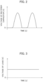
- a voltage waveform of the rectifier capacitor 73 has a shape subjected to half-wave rectification, the voltage waveform to be supplied to the load 13 via the LC filter becomes direct current, as illustrated in Fig. 3 .
- the detector 9 detects a change in impedance of the rectifier capacitor 73.
- the detector 9 detects a current value or a voltage value of the rectifier capacitor 73, and detects a degree of change in impedance of the rectifier capacitor 73 according to a change in the current value or the voltage value.
- the detector 9 may detect a temperature of the rectifier capacitor 73 so as to detect a degree of change in the impedance of the rectifier capacitor 73 according to a change in the temperature.
- the detector 9, when provided with any of an ammeter, a voltmeter, or a thermometer may detect a change in the impedance by calculating the amount of change in the value of any of the current, the voltage, or the temperature.
- the impedance of the rectifier capacitor 73 has a set value set so that the power conversion device 1 can execute optimum operations. The detector 9 thus detects how much the impedance of the rectifier capacitor 73 is changed from the set value.
- the controller 11 regulates the AC wave input to the rectifier capacitor 73 so as to suppress the change in the impedance of the rectifier capacitor 73, depending on the change in the impedance of the rectifier capacitor 73 detected by the detector 9.
- the controller 11 regulates the AC wave input to the rectifier capacitor 73 so as to decrease an output voltage of the power conversion device 1.
- the controller 11 regulates the AC wave input to the rectifier capacitor 73 so as to increase the output voltage of the power conversion device 1.
- the controller 11 changes the drive frequency of the switching element 57 to regulate a frequency of the AC wave generated in the AC wave generation circuit 5, so as to regulate the AC wave input to the rectifier capacitor 73.
- the controller 11 is fabricated by a multi-purpose electronic circuit including a microcomputer, a microprocessor, and a CPU, and peripheral components such as a memory, and has a function of controlling the AC wave generation circuit 5 and the rectifier circuit 7.
- the respective functions of the controller 11 can be implemented in single or plural processing circuits.
- the respective processing circuits include a programmed processing device, such as a processing device including an electric circuit, for example, and also include an application-specific integrated circuit (ASIC) configured to execute the functions described herein, and conventional circuit components.
- ASIC application-specific integrated circuit
- a method for controlling the power conversion device 1 according to the present embodiment is described below.
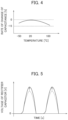
- a capacitance of the rectifier capacitor 73 included in the rectifier circuit 7 has the temperature characteristics as illustrated in Fig. 4 , and a capacitance value of the rectifier capacitor 73 thus decreases as the temperature of the rectifier capacitor 73 increases.
- the power conversion device 1 regulates the AC wave input to the rectifier capacitor 73 depending on the change in the impedance of the rectifier capacitor 73 detected by the detector 9 so as to suppress the change in the impedance of the rectifier capacitor 73.
- the controller 11 regulates the AC wave input to the rectifier capacitor 73 so as to decrease the output voltage of the power conversion device 1.
- the controller 11 regulates the AC wave input to the rectifier capacitor 73 so as to increase the output voltage of the power conversion device 1.
- the controller 11 changes the drive frequency of the switching element 57 to regulate the frequency of the AC wave generated in the AC wave generation circuit 5, so as to regulate the AC wave input to the rectifier capacitor 73.
- the impedance of the rectifier capacitor 73 is increased above the set value, and the voltage of the rectifier capacitor 73 is also increased, as given by the formula (1).
- the drive frequency of the switching element 57 is caused to increase above a predetermined value to increase the frequency of the AC wave generated by the AC wave generation circuit 5
- the frequency of the AC wave input to the rectifier circuit 7 is also increased.
- the value ⁇ in the formula (1) is then increased, and the impedance of the rectifier capacitor 73 is decreased accordingly. This leads the peak value of the voltage waveform of the rectifier capacitor 73 to be decreased as illustrated in Fig.
- the predetermined value set for the drive frequency may be a frequency obtained upon the execution of an optimum operation so that the load 13 has a design value.
- the impedance of the rectifier capacitor 73 is decreased below the set value, and the voltage of the rectifier capacitor 73 is also decreased, as given by the formula (1).
- the drive frequency of the switching element 57 is caused to decrease below the predetermined value to decrease the frequency of the AC wave generated by the AC wave generation circuit 5
- the frequency of the AC wave input to the rectifier circuit 7 is also decreased.
- the value ⁇ in the formula (1) is then decreased, and the impedance of the rectifier capacitor 73 is increased accordingly. This leads the peak value of the voltage waveform of the rectifier capacitor 73 to be increased, and also leads the output voltage of the power conversion device 1 output to the load 13 to be increased.
- regulating the frequency of the AC wave input to the rectifier capacitor 73 suppresses the change in the impedance of the rectifier capacitor 73.
- This can control the input impedance, the input current, and the output voltage of the power conversion device 1 each to be constant, so as to prevent over temperature of the components caused by thermal runaway.
- the AC wave generation circuit 5 is the class-E inverter circuit that can achieve zero-voltage switching (ZVS) due to voltage resonance, so as to greatly suppress the switching loss. This can reduce the influence which increases the drive frequency to a small level accordingly.
- ZVS zero-voltage switching
- the rectifier circuit 7 is the class-E circuit in which the diode 71 and the rectifier capacitor 73 are connected in parallel.
- other rectifier circuits such as full-wave rectifier circuits with diode, do not have a rectifier capacitor to charge energy.
- the rectifier circuit 7 thus does not cause a change in the output voltage, the input current, or the input impedance because of a change in the temperature of the rectifier capacitor, so as to prevent over temperature that is the problem to be solved by the present embodiment.
- snubber circuits While typical snubber circuits also employ a configuration in which a diode and a capacitor are connected in parallel, the snubber circuits execute an operation of absorbing a surge voltage derived from high-speed switching by the capacitor, and thus have a different function from the rectifier circuit 7 according to the present embodiment.
- the AC wave generation circuit 5 may have any configuration that generates and outputs the AC wave, instead of the configuration illustrated in Fig. 1 , and may be a resonant circuit including a plurality of switches, such as a class-D inverter circuit.
- the filter of the rectifier circuit 7 is not limited to the LC filter, and may have any structure.
- a transformer for isolation may be arranged between the AC wave generation circuit 5 and the rectifier circuit 7.
- the power conversion device 1 regulates the AC wave input to the rectifier capacitor 73 so as to suppress a change in the impedance of the rectifier capacitor 73, depending on the change in the impedance of the rectifier capacitor 73. This can suppress the change in the input current, the output voltage, and the input impedance of the power conversion device 1, so as to prevent over temperature of the rectifier capacitor 73.
- the power conversion device 1 regulates the AC wave input to the rectifier capacitor 73 so as to decrease the output voltage of the power conversion device 1 when the impedance of the rectifier capacitor 73 is increased above the set value.
- the power conversion device 1 regulates the AC wave input to the rectifier capacitor 73 so as to increase the output voltage of the power conversion device 1 when the impedance of the rectifier capacitor 73 is decreased below the set value.
- the power conversion device 1 can suppress the change in the impedance of the rectifier capacitor 73, so as to prevent over temperature of the rectifier capacitor 73.
- the power conversion device 1 increases the frequency of the AC wave generated by the AC wave generation circuit 5 when the impedance of the rectifier capacitor 73 is increased above the set value.
- the power conversion device 1 decreases the frequency of the AC wave generated by the AC wave generation circuit 5 when the impedance of the rectifier capacitor 73 is decreased below the set value.
- the power conversion device 1 can suppress the change in the impedance of the rectifier capacitor 73 by regulating the frequency of the AC wave input to the rectifier capacitor 73, so as to prevent over temperature of the rectifier capacitor 73.
- the power conversion device 1 detects the change in the impedance of the rectifier capacitor 73. Since the power conversion device 1 directly detects the change in the impedance of the rectifier capacitor 73, the power conversion device 1 can immediately suppress the change in the impedance of the rectifier capacitor 73, so as to prevent over temperature of the rectifier capacitor 73 with a high accuracy.
- the power conversion device 1 includes the AC wave generation circuit 5 that includes the resonant circuit including the resonant coil 53 and the resonant capacitor 55, and the switching element 57 that turns on/off the input to the resonant circuit.
- the power conversion device 1 can easily regulate the AC wave input to the rectifier capacitor 73 by regulating the drive frequency of the switching element 57. This can suppress the change in the impedance of the rectifier capacitor 73, so as to prevent over temperature of the rectifier capacitor 73.
- the power conversion device 1 includes the AC wave generation circuit 5 that further includes the choke coil 51 connected between the input power supply 3 and the switching element 57, and the shunt capacitor 59 connected in parallel to the switching element 57.
- the resonant circuit is connected to the connection point between the choke coil 51 and the switching element 57. Since the AC wave generation circuit 5 can be implemented as the class-E inverter circuit, a switching loss can be reduced to a small level. This can not only suppress an influence caused by an increase in switching loss upon the increase in the drive frequency of the switching element 57 but also prevent over temperature of the rectifier capacitor 73.
- Fig. 12 is a circuit diagram illustrating a configuration of a power conversion device according to the present embodiment. As illustrated in Fig. 12 , the power conversion device 1 according to the present embodiment differs from the first embodiment in further including a rectifier switch 79 as a switching element which turns on/off the AC wave input to the rectifier capacitor 73. The rectifier switch 79 is connected in series to the rectifier capacitor 73.
- a method for controlling the power conversion device 1 according to the present embodiment is described below.
- the controller 11 controls the on/off operation of the rectifier switch 79 so as to regulate the AC wave input to the rectifier capacitor 73.
- the controller 11 controls the rectifier switch 79 so as to decrease the period of time during which the AC wave is input to the rectifier capacitor 37.
- the controller 11 controls the rectifier switch 79 so as to increase the period of time during which the AC wave is input to the rectifier capacitor 37.
- an input stop period is provided at a point at which the voltage of the rectifier capacitor 73 starts increasing as illustrated in Fig. 13 .
- the input stop period is a period during which the rectifier switch 79 is turned off so as not to input the AC wave to the rectifier capacitor 73. After this period, the rectifier switch 79 is turned on so as to input the AC wave to the rectifier capacitor 73 (an AC wave input period).
- the AC wave input period is shorter as the input stop period is set to be longer, so as to set the period of time during which the AC wave is input to the rectifier capacitor 73 to be shorter than a predetermined time.
- the power to be charged to the rectifier capacitor 73 is thus reduced, so as to decrease the output voltage of the power conversion device 1 output to the load 13, as illustrated in Fig. 14 .
- the predetermined time may be set to a time upon the execution of an optimum operation so that the load 13 has a design value.
- the capacitance of the rectifier capacitor 73 is increased in association with a decrease in the temperature of the rectifier capacitor 73, the impedance of the rectifier capacitor 73 is decreased as given by the formula (1), and the voltage of the rectifier capacitor 73 is decreased.
- the input stop period as illustrated in Fig. 13 is decreased so as to set the period of time during which the AC wave is input to the rectifier capacitor 73 to be longer than the predetermined time. The power to be charged to the rectifier capacitor 73 is thus increased, so as to increase the output voltage of the power conversion device 1 output to the load 13.
- the rectifier switch 79 may be connected in parallel to the rectifier capacitor 73, as illustrated in Fig. 15 . In this case, the operation of turning on/off the rectifier switch 79 is controlled reversely to the case of being connected in series as illustrated in Fig. 12 . In particular, when the rectifier switch 79 is connected in parallel to the rectifier capacitor 73, by turning on the rectifier switch 79, the input stop period during which the AC wave is not input to the rectifier capacitor 73 is set. The AC wave is input to the rectifier capacitor 73 when the rectifier switch 79 is turned off.
- the power conversion device 1 decreases the period of time during which the AC wave is input to the rectifier capacitor 73 when the impedance of the rectifier capacitor 73 is increased above the set value.
- the power conversion device 1 increases the period of time during which the AC wave is input to the rectifier capacitor 73 when the impedance of the rectifier capacitor 73 is decreased below the set value.
- the power conversion device 1 can suppress the change in the impedance of the rectifier capacitor 73 by regulating the period of time during which the AC wave is input to the rectifier capacitor 73. As a result, the power conversion device 1 can prevent over temperature of the rectifier capacitor 73.
- Fig. 16 is a circuit diagram illustrating a configuration of a power conversion device according to the present embodiment.
- the power conversion device 1 according to the present embodiment differs from the first and second embodiments in detecting an input voltage, an input current, an output voltage, and an output current of the power conversion device 1.
- the detector 9 detects the input voltage Vi, the input current Ii, the output voltage Vo, and the output current Io of the power conversion device 1, instead of the change in the impedance of the rectifier capacitor 73. Since a typical power conversion device detects an input voltage, an input current, an output voltage, and an output current, these values may be detected by a general method such as installing a voltmeter or an ammeter in this embodiment,.
- the power conversion device 1 is controlled based on the input voltage Vi, the input current Ii, the output voltage Vo, and the output current Io of the power conversion device 1.
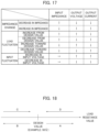
- the controller 11 determines whether the impedance of the rectifier capacitor 73 is increased above the set value or decreased below the set value, while referring to a table as illustrated in Fig. 17.
- Fig. 17 illustrates upward arrows indicating an increase, downward arrows indicating a decrease, and sideways arrows indicating no change.
- the controller 11 determines that the capacitance of the rectifier capacitor 73 is decreased and the impedance is increased above the set value.
- the controller 11 determines that the capacitance of the rectifier capacitor 73 is increased and the impedance is decreased below the set value.
- the set value for each of the input impedance, the output voltage, and the output current is a value when the power conversion device 1 executes an optimum operation.
- the controller 11 distinguishes between the case where the load 13 fluctuates and the case where the input voltage fluctuates based on the input impedance Zi, the output voltage Vo, and the output current Io.
- the controller 11 determines that this case corresponds to "change A" in which a resistance value of the load 13 is increased above the design value.
- the power conversion device 1 sets and determines the resistance value of the load 13 in optimum operation to 50 ⁇ as the design value, for example.
- the "change A” is a case in which the resistance value of the load 13 is increased in a direction away from the design value determined.
- the controller 11 determines that this case corresponds to "change B" as illustrated in Fig. 18 .
- the "change B” is a case in which the resistance value of the load 13 is decreased in the direction away from the design value.
- the controller 11 determines that this case corresponds to "change C" as illustrated in Fig. 18 .
- the "change C” is a case in which the resistance value of the load 13 is increased in the direction approaching the design value.
- the controller 11 determines that this case corresponds to "change D” as illustrated in Fig. 18 .
- the "change D” is a case in which the resistance value of the load 13 is decreased in the direction approaching the design value.
- the controller 11 determines that this case corresponds to an input fluctuation, and determines that the input voltage is increased when the output voltage Vo and the output current Io are increased above the set value. When the output voltage Vo and the output current Io are decreased below the set value, the controller 11 determines that input voltage is decreased.
- the controller 11 when determining the change in the impedance, controls the drive frequency of the switching element 57.
- the controller 11 when determining that the impedance of the rectifier capacitor 73 is increased above the set value, increases the drive frequency of the switching element 57 to decrease the impedance of the rectifier capacitor 73.
- Fig. 16 illustrates the case in which the power conversion device according to the present embodiment is applied to the power conversion device according to the first embodiment illustrated in Fig. 1
- the power conversion device according to the present embodiment may be applied to the power conversion device according to the second embodiment illustrated in Fig. 12 or Fig. 15 .
- the power conversion device 1 can determine all of the change in the impedance of the rectifier capacitor 73, the fluctuation in the load 13, and the fluctuation in the input voltage by use of the input impedance, the output voltage, and the output current of the power conversion device 1. It could be presumed that the impedance of the rectifier capacitor 73 is not necessarily changed even though the input impedance is changed, but the input impedance may be changed in response to the fluctuation in the load 13. In view of this, the power conversion device 1 according to the present embodiment accurately makes a determination of which case is caused, the change in the impedance of the rectifier capacitor 73, or the fluctuation in the input voltage or the fluctuation in the load 13, according to the table as illustrated in Fig. 17 .
- Another method could also be used that measures the temperature of the rectifier capacitor 73 and estimates the amount of change in the capacitance value according to the change in the temperature. This method, however, needs to add a measurement device for measuring the temperature at a specific point. Still another method could be used that accurately estimates the change in the capacitance value according to the value of the increase in the temperature. This method also needs to preliminarily measure the characteristics including a variation in each of capacitors, and further needs to add a checking process of acquiring a relationship between the temperature and the capacitance value for each of devices to be manufactured. This requires additional components for estimating the amount of change in the capacitance value according to the change in the temperature of the rectifier capacitor 73, impeding a reduction in size of the device or a reduction in cost.
- the power conversion device 1 detects the input voltage, the input current, the output voltage, and the output current of the power conversion device 1. Therefore, the power conversion device 1 only uses the voltage and the current of the input/output power which are typically detected. Thus, the power conversion device 1 can determine the change in the impedance of the rectifier capacitor 73 with no additional components provided for measuring the temperature. The power conversion device 1 thus can suppress the change in the impedance of the rectifier capacitor 73 with no addition of components or devices to prevent over temperature of the rectifier capacitor 73.
- the power conversion device 1 also calculates the input impedance according to the input voltage and the input current, and determines that the impedance of the rectifier capacitor 73 is increased above the set value when the input impedance is decreased below the set value and the output voltage and the output current are increased above the set value.
- the power conversion device 1 determines that the impedance of the rectifier capacitor 73 is decreased below the set value when the input impedance is increased above the set value and the output voltage and the output current are decreased below the set value.
- the power conversion device 1 can determine whether the impedance of the rectifier capacitor 73 is increased above or decreased below the set value, with no addition of components or devices. The power conversion device 1 thus can suppress the change in the impedance of the rectifier capacitor 73 based on this determination, so as to prevent over temperature of the rectifier capacitor 73.
- a method for controlling a power conversion device comprising an alternating-current wave generation circuit configured to generate an alternating-current wave, and a rectifier circuit configured to rectify the alternating-current wave generated by the alternating-current wave generation circuit with a configuration in which a rectifier capacitor and a diode are connected in parallel, the method comprising regulating the alternating-current wave input to the rectifier capacitor depending on a change in impedance of the rectifier capacitor so as to suppress the change in the impedance of the rectifier capacitor.
- a power conversion device comprising:
- the alternating-current wave generation circuit includes a resonant circuit including a resonant coil and a resonant capacitor, and a switching element configured to turn on or off an input to the resonant circuit.
Landscapes
- Engineering & Computer Science (AREA)
- Power Engineering (AREA)
- Rectifiers (AREA)
- Dc-Dc Converters (AREA)
- Inverter Devices (AREA)
Abstract
Description
- The present invention relates to a power conversion device including an alternating-current (AC) wave generation circuit for generating an AC wave and a rectifier circuit for rectifying the AC wave generated by the AC wave generation circuit with a configuration including a rectifier capacitor and a diode connected in parallel, and a method for controlling the power conversion device.
- Circuits for rectifying an AC wave are known, such as a class-E rectifier circuit as disclosed in
Patent Document 1. - Patent Document 1: International Publication
WO 2015/087396 - However, in the conventional class E-rectifier circuit described above, the capacitance value of the capacitor constituting the rectifier circuit changes depending on the temperature characteristics. For example, since the capacitance of the capacitor decreases as the temperature increases, a peak value of a voltage waveform subjected to half-wave rectification in the rectifier circuit increases in association with the decrease in the capacitance, leading to a decrease in impedance. After that, since the temperature of the capacitor rises further, the same phenomenon is repeated, and there is a problem that over temperature occurs beyond a rated temperature of components.
- In view of the foregoing problem, the present invention provides a power conversion device capable of suppressing a change in impedance of a capacitor included in a rectifier circuit to prevent over temperature, and a method for controlling the power conversion device.
- To solve the above problem, an aspect of the present invention provides a power conversion device and a method for controlling the power conversion device configured to regulate an alternating-current wave input to a rectifier capacitor depending on a change in impedance of the rectifier capacitor so as to suppress the change in the impedance of the rectifier capacitor.
- The present invention can suppress a change in impedance of a rectifier capacitor included in a rectifier circuit to prevent over temperature in the rectifier capacitor.
-
- [
Fig. 1] Fig. 1 is a circuit diagram illustrating a configuration of a power conversion device according to a first embodiment of the present invention. - [
Fig. 2] Fig. 2 is a diagram illustrating a voltage of a rectifier capacitor included in the power conversion device according to the first embodiment of the present invention. - [
Fig. 3] Fig. 3 is a diagram illustrating an output voltage of the power conversion device according to the first embodiment of the present invention. - [
Fig. 4] Fig. 4 is a diagram illustrating temperature characteristics of a capacitance of the rectifier capacitor included in the power conversion device according to the first embodiment of the present invention. - [
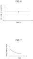
Fig. 5] Fig. 5 is a diagram illustrating a change in voltage of the rectifier capacitor included in the power conversion device according to the first embodiment of the present invention. - [
Fig. 6] Fig. 6 is a diagram illustrating a change in the output voltage of the power conversion device according to the first embodiment of the present invention. - [
Fig. 7] Fig. 7 is a diagram illustrating a change with time in input impedance of a conventional power conversion device. - [
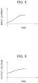
Fig. 8] Fig. 8 is a diagram illustrating a change with time in input current of the conventional power conversion device. - [
Fig. 9] Fig. 9 is a diagram illustrating a change with time in output voltage of the conventional power conversion device. - [
Fig. 10] Fig. 10 is a diagram illustrating a change in voltage of the rectifier capacitor included in the power conversion device according to the first embodiment of the present invention. - [
Fig. 11] Fig. 11 is a diagram illustrating a change in the output voltage of the power conversion device according to the first embodiment of the present invention. - [
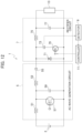
Fig. 12] Fig. 12 is a circuit diagram illustrating a configuration of a power conversion device according to a second embodiment of the present invention. - [
Fig. 13] Fig. 13 is a diagram illustrating a change in voltage of a rectifier capacitor included in the power conversion device according to the second embodiment of the present invention. - [
Fig. 14] Fig. 14 is a diagram illustrating a change in output voltage of the power conversion device according to the second embodiment of the present invention. - [
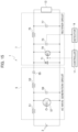
Fig. 15] Fig. 15 is a circuit diagram illustrating a configuration of the power conversion device according to the second embodiment of the present invention. - [
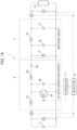
Fig. 16] Fig. 16 is a circuit diagram illustrating a configuration of a power conversion device according to a third embodiment of the present invention. - [
Fig. 17] Fig. 17 is a diagram for explaining a method of determining a change in impedance of a rectifier capacitor included in the power conversion device according to the third embodiment of the present invention. - [
Fig. 18] Fig. 18 is a diagram for explaining a load fluctuation in the power conversion device according to the third embodiment of the present invention. - A first embodiment to which the present invention is applied is described below with reference to the drawings. The same elements illustrated with reference to the drawings are indicated by the same reference numerals, and overlapping explanations are not repeated below.
-
Fig. 1 is a circuit diagram illustrating a configuration of a power conversion device according to the present embodiment. As illustrated inFig. 1 , thepower conversion device 1 according to the present embodiment includes aninput power supply 3, an alternating-current (AC)wave generation circuit 5, arectifier circuit 7, a detector 9, acontroller 11, and aload 13. Thepower conversion device 1 converts direct current (DC) power input from theinput power supply 3 into AC power, and supplies DC power rectified by therectifier circuit 7 to theload 13. - The AC
wave generation circuit 5 includes achoke coil 51, aresonant coil 53, aresonant capacitor 55, aswitching element 57, and ashunt capacitor 59. The ACwave generation circuit 5 is a class-E inverter circuit that generates an AC wave from the DC power from theinput power supply 3 depending on a drive frequency of theswitching element 57. - As illustrated in
Fig. 1 , thechoke coil 51 is connected between theinput power supply 3 and theswitching element 57. Theresonant coil 53 and theresonant capacitor 55 form a resonant circuit connected to a connection point between thechoke coil 51 and theswitching element 57. Theswitching element 57 turns on/off the input to the resonant circuit. Theshunt capacitor 59 is connected in parallel to theswitching element 57. - The
rectifier circuit 7 is a class-E circuit that includes adiode 71, arectifier capacitor 73, afilter coil 75, and afilter capacitor 77 to rectify an AC wave with a configuration in which thediode 71 and therectifier capacitor 73 are connected in parallel. - The
rectifier circuit 7 causes thediode 71 to subject the AC wave generated in the ACwave generation circuit 5 to half-wave rectification to charge the rectified energy to therectifier capacitor 73. Therectifier circuit 7 transfers the charged energy to an LC filter implemented by thefilter coil 75 and thefilter capacitor 77 to transmit the power in a DC waveform to theload 13. As illustrated inFig. 2 , while a voltage waveform of therectifier capacitor 73 has a shape subjected to half-wave rectification, the voltage waveform to be supplied to theload 13 via the LC filter becomes direct current, as illustrated inFig. 3 . - The detector 9 detects a change in impedance of the
rectifier capacitor 73. The detector 9 detects a current value or a voltage value of therectifier capacitor 73, and detects a degree of change in impedance of therectifier capacitor 73 according to a change in the current value or the voltage value. The detector 9 may detect a temperature of therectifier capacitor 73 so as to detect a degree of change in the impedance of therectifier capacitor 73 according to a change in the temperature. The detector 9, when provided with any of an ammeter, a voltmeter, or a thermometer, may detect a change in the impedance by calculating the amount of change in the value of any of the current, the voltage, or the temperature. The impedance of therectifier capacitor 73 has a set value set so that thepower conversion device 1 can execute optimum operations. The detector 9 thus detects how much the impedance of therectifier capacitor 73 is changed from the set value. - The
controller 11 regulates the AC wave input to therectifier capacitor 73 so as to suppress the change in the impedance of therectifier capacitor 73, depending on the change in the impedance of therectifier capacitor 73 detected by the detector 9. In particular, when the impedance of therectifier capacitor 73 is increased above the set value, thecontroller 11 regulates the AC wave input to therectifier capacitor 73 so as to decrease an output voltage of thepower conversion device 1. When the impedance of therectifier capacitor 73 is decreased below the set value, thecontroller 11 regulates the AC wave input to therectifier capacitor 73 so as to increase the output voltage of thepower conversion device 1. For example, thecontroller 11 changes the drive frequency of theswitching element 57 to regulate a frequency of the AC wave generated in the ACwave generation circuit 5, so as to regulate the AC wave input to therectifier capacitor 73. - The
controller 11 is fabricated by a multi-purpose electronic circuit including a microcomputer, a microprocessor, and a CPU, and peripheral components such as a memory, and has a function of controlling the ACwave generation circuit 5 and therectifier circuit 7. The respective functions of thecontroller 11 can be implemented in single or plural processing circuits. The respective processing circuits include a programmed processing device, such as a processing device including an electric circuit, for example, and also include an application-specific integrated circuit (ASIC) configured to execute the functions described herein, and conventional circuit components. - A method for controlling the
power conversion device 1 according to the present embodiment is described below. A capacitance of therectifier capacitor 73 included in therectifier circuit 7 has the temperature characteristics as illustrated inFig. 4 , and a capacitance value of therectifier capacitor 73 thus decreases as the temperature of therectifier capacitor 73 increases. - A voltage V of the
rectifier capacitor 73 is inversely proportional to a capacitance value C of therectifier capacitor 73, as given by the following formula (1):
rectifier capacitor 73, ω = 2πf, and f is a frequency of an AC wave, which is the same as the drive frequency of the switchingelement 57. - According to the formula (1), since the voltage V of the
rectifier capacitor 73 increases as the capacitance value C of therectifier capacitor 73 decreases, a peak value of the voltage waveform of therectifier capacitor 73 increases in association with the decrease in the capacitance, as illustrated inFig. 5 . The output voltage of thepower conversion device 1 output to theload 13 then increases, as illustrated inFig. 6 . - At this time, since the input current of the
power conversion device 1 also increases, an input impedance of thepower conversion device 1 decreases. The temperature of therectifier capacitor 73 further increases in association with the increase in the input current and the output voltage, and the similar phenomenon is repeated accordingly. Therefore, in the conventional case, the input impedance of thepower conversion device 1 decreases with the passage of time, as illustrated inFig. 7 , and both the input current and the output voltage of thepower conversion device 1 increase, as illustrated inFig. 8 and Fig. 9 . As a result, the temperature of the circuit components increases with the time, causing over temperature due to thermal runaway accordingly. - However, according to the present embodiment, the
power conversion device 1 regulates the AC wave input to therectifier capacitor 73 depending on the change in the impedance of therectifier capacitor 73 detected by the detector 9 so as to suppress the change in the impedance of therectifier capacitor 73. In particular, when the impedance of therectifier capacitor 73 is increased above the set value, thecontroller 11 regulates the AC wave input to therectifier capacitor 73 so as to decrease the output voltage of thepower conversion device 1. On the other hand, when the impedance of therectifier capacitor 73 is decreased below the set value, thecontroller 11 regulates the AC wave input to therectifier capacitor 73 so as to increase the output voltage of thepower conversion device 1. - For example, the
controller 11 changes the drive frequency of the switchingelement 57 to regulate the frequency of the AC wave generated in the ACwave generation circuit 5, so as to regulate the AC wave input to therectifier capacitor 73. - More particularly, when the capacitance of the
rectifier capacitor 73 is decreased because of the increase in the temperature, the impedance of therectifier capacitor 73 is increased above the set value, and the voltage of therectifier capacitor 73 is also increased, as given by the formula (1). In this case, when the drive frequency of the switchingelement 57 is caused to increase above a predetermined value to increase the frequency of the AC wave generated by the ACwave generation circuit 5, the frequency of the AC wave input to therectifier circuit 7 is also increased. As a result, the value ω in the formula (1) is then increased, and the impedance of therectifier capacitor 73 is decreased accordingly. This leads the peak value of the voltage waveform of therectifier capacitor 73 to be decreased as illustrated inFig. 10 , and also leads the output voltage of thepower conversion device 1 output to theload 13 to be decreased as illustrated inFig. 11 . The predetermined value set for the drive frequency may be a frequency obtained upon the execution of an optimum operation so that theload 13 has a design value. - When the capacitance of the
rectifier capacitor 73 is increased because of the decrease in the temperature, the impedance of therectifier capacitor 73 is decreased below the set value, and the voltage of therectifier capacitor 73 is also decreased, as given by the formula (1). In this case, when the drive frequency of the switchingelement 57 is caused to decrease below the predetermined value to decrease the frequency of the AC wave generated by the ACwave generation circuit 5, the frequency of the AC wave input to therectifier circuit 7 is also decreased. As a result, the value ω in the formula (1) is then decreased, and the impedance of therectifier capacitor 73 is increased accordingly. This leads the peak value of the voltage waveform of therectifier capacitor 73 to be increased, and also leads the output voltage of thepower conversion device 1 output to theload 13 to be increased. - As described above, regulating the frequency of the AC wave input to the
rectifier capacitor 73 suppresses the change in the impedance of therectifier capacitor 73. This can control the input impedance, the input current, and the output voltage of thepower conversion device 1 each to be constant, so as to prevent over temperature of the components caused by thermal runaway. - If the drive frequency of the switching
element 57 is increased, a switching loss is increased. In view of this, the ACwave generation circuit 5 is the class-E inverter circuit that can achieve zero-voltage switching (ZVS) due to voltage resonance, so as to greatly suppress the switching loss. This can reduce the influence which increases the drive frequency to a small level accordingly. - The
rectifier circuit 7 according to the present embodiment is the class-E circuit in which thediode 71 and therectifier capacitor 73 are connected in parallel. However, other rectifier circuits, such as full-wave rectifier circuits with diode, do not have a rectifier capacitor to charge energy. Therectifier circuit 7 thus does not cause a change in the output voltage, the input current, or the input impedance because of a change in the temperature of the rectifier capacitor, so as to prevent over temperature that is the problem to be solved by the present embodiment. - While typical snubber circuits also employ a configuration in which a diode and a capacitor are connected in parallel, the snubber circuits execute an operation of absorbing a surge voltage derived from high-speed switching by the capacitor, and thus have a different function from the
rectifier circuit 7 according to the present embodiment. - The AC
wave generation circuit 5 may have any configuration that generates and outputs the AC wave, instead of the configuration illustrated inFig. 1 , and may be a resonant circuit including a plurality of switches, such as a class-D inverter circuit. The filter of therectifier circuit 7 is not limited to the LC filter, and may have any structure. In addition, a transformer for isolation may be arranged between the ACwave generation circuit 5 and therectifier circuit 7. - As described in detail above, the
power conversion device 1 according to the present embodiment regulates the AC wave input to therectifier capacitor 73 so as to suppress a change in the impedance of therectifier capacitor 73, depending on the change in the impedance of therectifier capacitor 73. This can suppress the change in the input current, the output voltage, and the input impedance of thepower conversion device 1, so as to prevent over temperature of therectifier capacitor 73. - The
power conversion device 1 according to the present embodiment regulates the AC wave input to therectifier capacitor 73 so as to decrease the output voltage of thepower conversion device 1 when the impedance of therectifier capacitor 73 is increased above the set value. Thepower conversion device 1 regulates the AC wave input to therectifier capacitor 73 so as to increase the output voltage of thepower conversion device 1 when the impedance of therectifier capacitor 73 is decreased below the set value. Thus thepower conversion device 1 can suppress the change in the impedance of therectifier capacitor 73, so as to prevent over temperature of therectifier capacitor 73. - The
power conversion device 1 according to the present embodiment increases the frequency of the AC wave generated by the ACwave generation circuit 5 when the impedance of therectifier capacitor 73 is increased above the set value. Thepower conversion device 1 decreases the frequency of the AC wave generated by the ACwave generation circuit 5 when the impedance of therectifier capacitor 73 is decreased below the set value. Thepower conversion device 1 can suppress the change in the impedance of therectifier capacitor 73 by regulating the frequency of the AC wave input to therectifier capacitor 73, so as to prevent over temperature of therectifier capacitor 73. - The
power conversion device 1 according to the present embodiment detects the change in the impedance of therectifier capacitor 73. Since thepower conversion device 1 directly detects the change in the impedance of therectifier capacitor 73, thepower conversion device 1 can immediately suppress the change in the impedance of therectifier capacitor 73, so as to prevent over temperature of therectifier capacitor 73 with a high accuracy. - The
power conversion device 1 according to the present embodiment includes the ACwave generation circuit 5 that includes the resonant circuit including theresonant coil 53 and theresonant capacitor 55, and the switchingelement 57 that turns on/off the input to the resonant circuit. Thus, thepower conversion device 1 can easily regulate the AC wave input to therectifier capacitor 73 by regulating the drive frequency of the switchingelement 57. This can suppress the change in the impedance of therectifier capacitor 73, so as to prevent over temperature of therectifier capacitor 73. - The
power conversion device 1 according to the present embodiment includes the ACwave generation circuit 5 that further includes thechoke coil 51 connected between theinput power supply 3 and the switchingelement 57, and theshunt capacitor 59 connected in parallel to the switchingelement 57. The resonant circuit is connected to the connection point between thechoke coil 51 and the switchingelement 57. Since the ACwave generation circuit 5 can be implemented as the class-E inverter circuit, a switching loss can be reduced to a small level. This can not only suppress an influence caused by an increase in switching loss upon the increase in the drive frequency of the switchingelement 57 but also prevent over temperature of therectifier capacitor 73. - A second embodiment to which the present invention is applied is described below with reference to the drawings. The same elements illustrated with reference to the drawings are indicated by the same reference numerals, and overlapping explanations are not repeated below.
-
Fig. 12 is a circuit diagram illustrating a configuration of a power conversion device according to the present embodiment. As illustrated inFig. 12 , thepower conversion device 1 according to the present embodiment differs from the first embodiment in further including arectifier switch 79 as a switching element which turns on/off the AC wave input to therectifier capacitor 73. Therectifier switch 79 is connected in series to therectifier capacitor 73. - A method for controlling the
power conversion device 1 according to the present embodiment is described below. According to the present embodiment, when the detector 9 detects a change in the impedance of therectifier capacitor 73, thecontroller 11 controls the on/off operation of therectifier switch 79 so as to regulate the AC wave input to therectifier capacitor 73. - In particular, when the impedance of the
rectifier capacitor 73 is increased above the set value, thecontroller 11 controls therectifier switch 79 so as to decrease the period of time during which the AC wave is input to the rectifier capacitor 37. When the impedance of therectifier capacitor 73 is decreased below the set value, thecontroller 11 controls therectifier switch 79 so as to increase the period of time during which the AC wave is input to the rectifier capacitor 37. - For example, when the capacitance of the
rectifier capacitor 73 is decreased in association with an increase in the temperature of therectifier capacitor 73, the impedance of therectifier capacitor 73 is increased as given by the formula (1), and the voltage of therectifier capacitor 73 is increased. In this case, an input stop period is provided at a point at which the voltage of therectifier capacitor 73 starts increasing as illustrated inFig. 13 . The input stop period is a period during which therectifier switch 79 is turned off so as not to input the AC wave to therectifier capacitor 73. After this period, therectifier switch 79 is turned on so as to input the AC wave to the rectifier capacitor 73 (an AC wave input period). The AC wave input period is shorter as the input stop period is set to be longer, so as to set the period of time during which the AC wave is input to therectifier capacitor 73 to be shorter than a predetermined time. The power to be charged to therectifier capacitor 73 is thus reduced, so as to decrease the output voltage of thepower conversion device 1 output to theload 13, as illustrated inFig. 14 . The predetermined time may be set to a time upon the execution of an optimum operation so that theload 13 has a design value. - When the capacitance of the
rectifier capacitor 73 is increased in association with a decrease in the temperature of therectifier capacitor 73, the impedance of therectifier capacitor 73 is decreased as given by the formula (1), and the voltage of therectifier capacitor 73 is decreased. In this case, the input stop period as illustrated inFig. 13 is decreased so as to set the period of time during which the AC wave is input to therectifier capacitor 73 to be longer than the predetermined time. The power to be charged to therectifier capacitor 73 is thus increased, so as to increase the output voltage of thepower conversion device 1 output to theload 13. - The
rectifier switch 79 may be connected in parallel to therectifier capacitor 73, as illustrated inFig. 15 . In this case, the operation of turning on/off therectifier switch 79 is controlled reversely to the case of being connected in series as illustrated inFig. 12 . In particular, when therectifier switch 79 is connected in parallel to therectifier capacitor 73, by turning on therectifier switch 79, the input stop period during which the AC wave is not input to therectifier capacitor 73 is set. The AC wave is input to therectifier capacitor 73 when therectifier switch 79 is turned off. - As described above, the
power conversion device 1 according to the present embodiment decreases the period of time during which the AC wave is input to therectifier capacitor 73 when the impedance of therectifier capacitor 73 is increased above the set value. Thepower conversion device 1 increases the period of time during which the AC wave is input to therectifier capacitor 73 when the impedance of therectifier capacitor 73 is decreased below the set value. Thepower conversion device 1 can suppress the change in the impedance of therectifier capacitor 73 by regulating the period of time during which the AC wave is input to therectifier capacitor 73. As a result, thepower conversion device 1 can prevent over temperature of therectifier capacitor 73. - A third embodiment to which the present invention is applied is described below with reference to the drawings. The same elements illustrated with reference to the drawings are indicated by the same reference numerals, and overlapping explanations are not repeated below.
-
Fig. 16 is a circuit diagram illustrating a configuration of a power conversion device according to the present embodiment. As illustrated inFig. 16 , thepower conversion device 1 according to the present embodiment differs from the first and second embodiments in detecting an input voltage, an input current, an output voltage, and an output current of thepower conversion device 1. The detector 9 detects the input voltage Vi, the input current Ii, the output voltage Vo, and the output current Io of thepower conversion device 1, instead of the change in the impedance of therectifier capacitor 73. Since a typical power conversion device detects an input voltage, an input current, an output voltage, and an output current, these values may be detected by a general method such as installing a voltmeter or an ammeter in this embodiment,. - A method for controlling the
power conversion device 1 according to the present embodiment is described below. According to the present embodiment, thepower conversion device 1 is controlled based on the input voltage Vi, the input current Ii, the output voltage Vo, and the output current Io of thepower conversion device 1. In particular, thecontroller 11 first acquires the input voltage Vi, the input current Ii, the output voltage Vo, and the output current Io from the detector 9, and calculates an input impedance Zi according to the following formula (2):
- After calculating the input impedance Zi, The
controller 11 determines whether the impedance of therectifier capacitor 73 is increased above the set value or decreased below the set value, while referring to a table as illustrated inFig. 17. Fig. 17 illustrates upward arrows indicating an increase, downward arrows indicating a decrease, and sideways arrows indicating no change. - As illustrated in
Fig. 17 , when the input impedance Zi is decreased below the set value, and the output voltage Vo and the output current Io are increased above the set value, thecontroller 11 determines that the capacitance of therectifier capacitor 73 is decreased and the impedance is increased above the set value. When the input impedance Zi is increased above the set value, and the output voltage Vo and the output current Io are decreased below the set value, thecontroller 11 determines that the capacitance of therectifier capacitor 73 is increased and the impedance is decreased below the set value. The set value for each of the input impedance, the output voltage, and the output current is a value when thepower conversion device 1 executes an optimum operation. - When a change in the input/output power of the
power conversion device 1 is caused, not only a change in the capacitance of therectifier capacitor 73 but also a fluctuation in theload 13 and the input voltage are presumed. Therefore, thecontroller 11 distinguishes between the case where theload 13 fluctuates and the case where the input voltage fluctuates based on the input impedance Zi, the output voltage Vo, and the output current Io. - The case of the fluctuation in the
load 13 is described first. As illustrated inFig. 17 , when the input impedance Zi and the output voltage Vo is increased above the set value, and the output current Io is decreased below the set value, thecontroller 11 determines that this case corresponds to "change A" in which a resistance value of theload 13 is increased above the design value. For example, as illustrated inFig. 18 , thepower conversion device 1 sets and determines the resistance value of theload 13 in optimum operation to 50 Ω as the design value, for example. The "change A" is a case in which the resistance value of theload 13 is increased in a direction away from the design value determined. - Further, as illustrated in
Fig. 17 , when the input impedance Zi and the output current Io is increased above the set value, and the output voltage Vo is decreased below the set value, thecontroller 11 determines that this case corresponds to "change B" as illustrated inFig. 18 . The "change B" is a case in which the resistance value of theload 13 is decreased in the direction away from the design value. - Further, as illustrated in
Fig. 17 , when the input impedance Zi and the output current Io is decreased below the set value, and the output voltage Vo is increased above the set value, thecontroller 11 determines that this case corresponds to "change C" as illustrated inFig. 18 . The "change C" is a case in which the resistance value of theload 13 is increased in the direction approaching the design value. Further, as illustrated inFig. 17 , when the input impedance Zi and the output voltage Vo is decreased below the set value, and the output current Io is increased above the set value, thecontroller 11 determines that this case corresponds to "change D" as illustrated inFig. 18 . The "change D" is a case in which the resistance value of theload 13 is decreased in the direction approaching the design value. - The case of the fluctuation in the input voltage is described next. As illustrated in
Fig. 17 , when the input impedance Zi has no change from the set value, thecontroller 11 determines that this case corresponds to an input fluctuation, and determines that the input voltage is increased when the output voltage Vo and the output current Io are increased above the set value. When the output voltage Vo and the output current Io are decreased below the set value, thecontroller 11 determines that input voltage is decreased. - As described above, when any of the change in the impedance of the
rectifier capacitor 73, the fluctuation in theload 13, or the fluctuation in the input voltage is determined, thecontroller 11, when determining the change in the impedance, controls the drive frequency of the switchingelement 57. In particular, thecontroller 11, when determining that the impedance of therectifier capacitor 73 is increased above the set value, increases the drive frequency of the switchingelement 57 to decrease the impedance of therectifier capacitor 73. Thecontroller 11, when determining that the impedance of therectifier capacitor 73 is decreased below the set value, decreases the drive frequency of the switchingelement 57 to increase the impedance of therectifier capacitor 73. - While
Fig. 16 illustrates the case in which the power conversion device according to the present embodiment is applied to the power conversion device according to the first embodiment illustrated inFig. 1 , the power conversion device according to the present embodiment may be applied to the power conversion device according to the second embodiment illustrated inFig. 12 orFig. 15 . - As described above, the
power conversion device 1 according to the present embodiment can determine all of the change in the impedance of therectifier capacitor 73, the fluctuation in theload 13, and the fluctuation in the input voltage by use of the input impedance, the output voltage, and the output current of thepower conversion device 1. It could be presumed that the impedance of therectifier capacitor 73 is not necessarily changed even though the input impedance is changed, but the input impedance may be changed in response to the fluctuation in theload 13. In view of this, thepower conversion device 1 according to the present embodiment accurately makes a determination of which case is caused, the change in the impedance of therectifier capacitor 73, or the fluctuation in the input voltage or the fluctuation in theload 13, according to the table as illustrated inFig. 17 . - Another method could also be used that measures the temperature of the
rectifier capacitor 73 and estimates the amount of change in the capacitance value according to the change in the temperature. This method, however, needs to add a measurement device for measuring the temperature at a specific point. Still another method could be used that accurately estimates the change in the capacitance value according to the value of the increase in the temperature. This method also needs to preliminarily measure the characteristics including a variation in each of capacitors, and further needs to add a checking process of acquiring a relationship between the temperature and the capacitance value for each of devices to be manufactured. This requires additional components for estimating the amount of change in the capacitance value according to the change in the temperature of therectifier capacitor 73, impeding a reduction in size of the device or a reduction in cost. - On the contrary, the
power conversion device 1 according to the present embodiment detects the input voltage, the input current, the output voltage, and the output current of thepower conversion device 1. Therefore, thepower conversion device 1 only uses the voltage and the current of the input/output power which are typically detected. Thus, thepower conversion device 1 can determine the change in the impedance of therectifier capacitor 73 with no additional components provided for measuring the temperature. Thepower conversion device 1 thus can suppress the change in the impedance of therectifier capacitor 73 with no addition of components or devices to prevent over temperature of therectifier capacitor 73. - The
power conversion device 1 according to the present embodiment also calculates the input impedance according to the input voltage and the input current, and determines that the impedance of therectifier capacitor 73 is increased above the set value when the input impedance is decreased below the set value and the output voltage and the output current are increased above the set value. Thepower conversion device 1 determines that the impedance of therectifier capacitor 73 is decreased below the set value when the input impedance is increased above the set value and the output voltage and the output current are decreased below the set value. Thepower conversion device 1 can determine whether the impedance of therectifier capacitor 73 is increased above or decreased below the set value, with no addition of components or devices. Thepower conversion device 1 thus can suppress the change in the impedance of therectifier capacitor 73 based on this determination, so as to prevent over temperature of therectifier capacitor 73. - The embodiments described above are an example of the present invention. It should be understood that the present invention is not intended to be limited to these embodiments, and various modification can be made, in addition to the embodiments described above, depending on the design without departing from the scope of the technical idea of the present invention.
- The invention is also described by the following clauses:
- A method for controlling a power conversion device comprising an alternating-current wave generation circuit configured to generate an alternating-current wave, and a rectifier circuit configured to rectify the alternating-current wave generated by the alternating-current wave generation circuit with a configuration in which a rectifier capacitor and a diode are connected in parallel,
the method comprising regulating the alternating-current wave input to the rectifier capacitor depending on a change in impedance of the rectifier capacitor so as to suppress the change in the impedance of the rectifier capacitor. - The method for controlling the power conversion device according to
clause 1, further comprising: - regulating the alternating-current wave input to the rectifier capacitor so as to decrease an output voltage of the power conversion device when the impedance of the rectifier capacitor is increased above a set value; and
- regulating the alternating-current wave input to the rectifier capacitor so as to increase the output voltage of the power conversion device when the impedance of the rectifier capacitor is decreased below the set value.
- The method for controlling the power conversion device according to
clause 1 or 2, further comprising: - increasing a frequency of the alternating-current wave generated by the alternating-current wave generation circuit when the impedance of the rectifier capacitor is increased above the set value; and
- decreasing the frequency of the alternating-current wave generated by the alternating-current wave generation circuit when the impedance of the rectifier capacitor is decreased below the set value.
- The method for controlling the power conversion device according to
clause 1 or 2, further comprising: - decreasing a time during which the alternating-current wave is input to the rectifier capacitor when the impedance of the rectifier capacitor is increased above the set value; and
- increasing the time during which the alternating-current wave is input to the rectifier capacitor when the impedance of the rectifier capacitor is decreased below the set value.
- The method for controlling the power conversion device according to any one of
clauses 1 to 4, further comprising detecting the change in the impedance of the rectifier capacitor. - The method for controlling the power conversion device according to any one of
clauses 1 to 4, further comprising detecting an input voltage, an input current, an output voltage, and an output current of the power conversion device. - The method for controlling the power conversion device according to
clause 6, further comprising: - calculating an input impedance according to the input voltage and the input current;
- determining that the impedance of the rectifier capacitor is increased above the set value when the input impedance is decreased below the set value and the output voltage and the output current are increased above the set value; and
- determining that the impedance of the rectifier capacitor is decreased below the set value when the input impedance is increased above the set value and the output voltage and the output current are decreased below the set value.
- A power conversion device comprising:
- an alternating-current wave generation circuit configured to generate an alternating-current wave;
- a rectifier circuit configured to rectify the alternating-current wave generated by the alternating-current wave generation circuit with a configuration in which a rectifier capacitor and a diode are connected in parallel; and
- a controller configured to control the alternating-current generation circuit and the rectifier circuit,
- the controller being configured to regulate the alternating-current wave input to the rectifier capacitor depending on a change in impedance of the rectifier capacitor so as to suppress the change in the impedance of the rectifier capacitor.
- The power conversion device according to clause 8, wherein the alternating-current wave generation circuit includes a resonant circuit including a resonant coil and a resonant capacitor, and a switching element configured to turn on or off an input to the resonant circuit.
- The power conversion device according to clause 9, wherein:
- the alternating-current wave generation circuit further includes a choke coil connected between the switching element and a power supply, and a capacitor connected in parallel to the switching element; and
- the resonant circuit is connected to a connection point between the choke coil and the switching element.
-
- 1
- POWER CONVERSION DEVICE
- 3
- INPUT POWER SUPPLY
- 5
- AC WAVE GENERATION CIRCUIT
- 7
- RECTIFIER CIRCUIT
- 9
- DETECTOR
- 11
- CONTROLLER
- 13
- LOAD
- 51
- CHOKE COIL
- 53
- RESONANT COIL
- 55
- RESONANT CAPACITOR
- 57
- SWITCHING ELEMENT
- 59
- SHUNT CAPACITOR
- 71
- DIODE
- 73
- RECTIFIER CAPACITOR
- 75
- FILTER COIL
- 77
- FILTER CAPACITOR
- 79
- RECTIFIER SWITCH
Claims (7)
- A method for controlling a power conversion device (1),the power conversion device (1) comprising:- an alternating-current wave generation circuit (5) comprising a switching element (57) and configured to convert input power into an alternating-current wave,- a controller (11) configured to control the switching element (57) to regulate the alternating-current wave, and- a rectifier circuit (7)- which is configured to rectify the alternating-current wave generated by the alternating-current wave generation circuit (5) with a configuration in which a rectifier capacitor (73) and a diode (71) to subject the alternating-current wave to half-wave rectification are connected in parallel, and- which comprises:- a filter (75; 77) that is implemented by a filter coil (75) and a filter capacitor (77),the method comprising detecting an impedance of the rectifier capacitor (73), andthe method further comprising - by controlling a drive frequency of the switching element (57) -- regulating the alternating-current wave input to the rectifier capacitor (73) by the controller (11) so as to decrease an output voltage of the power conversion device (1) when the impedance of the rectifier capacitor (73) is increased above a set value; and- regulating the alternating-current wave input to the rectifier capacitor (73) by the controller (11) so as to increase the output voltage of the power conversion device (1) when the impedance of the rectifier capacitor (73) is decreased below the set value,- in order to thereby suppress a change in the impedance of the rectifier capacitor (73) by regulating the period of time during which the AC wave is input to the rectifier capacitor (73).
- The method according to claim 1, further comprising, by changing the drive frequency of the switching element (57) in the alternating-current wave generation circuit (5):- increasing a frequency of the alternating-current wave generated by the alternating-current wave generation circuit (5) when the impedance of the rectifier capacitor (73) is increased above the set value; and- decreasing the frequency of the alternating-current wave generated by the alternating-current wave generation circuit (5) when the impedance of the rectifier capacitor (73) is decreased below the set value.
- The method according to any one of the preceding claims, further comprising detecting an input voltage, an input current, an output voltage, and an output current of the power conversion device (1).
- The method according to claim 3, further comprising:- calculating an input impedance according to the input voltage and the input current;- determining that the impedance of the rectifier capacitor (73) is increased above the set value when the input impedance is decreased below the set value and the output voltage and the output current are increased above the set value; and- determining that the impedance of the rectifier capacitor (73) is decreased below the set value when the input impedance is increased above the set value and the output voltage and the output current are decreased below the set value.
- A power conversion device (1),comprising:- an alternating-current wave generation circuit (5) comprising a switching element (57) and configured to convert input power into an alternating-current wave;- a controller (11) configured to control the switching element (57) to regulate the alternating-current wave; and- a rectifier circuit (7)- which is configured to rectify the alternating-current wave generated by the alternating-current wave generation circuit (5) with a configuration in which a rectifier capacitor (73) and a diode (71) to subject the alternating-current wave to half-wave rectification are connected in parallel; and- which comprises:- a filter (75; 77) that is implemented by a filter coil (75) and a filter capacitor (77), andwherein the controller (11) is configured:- to control the alternating-current generation circuit (5),- to detect an impedance of the rectifier capacitor (73), and- to control a drive frequency of the switching element (57) in order- to regulate the alternating-current wave input to the rectifier capacitor (73) so as to decrease an output voltage of the power conversion device (1) when the impedance of the rectifier capacitor (73) is increased above a set value; and- to regulate the alternating-current wave input to the rectifier capacitor (73) so as to increase the output voltage of the power conversion device (1) when the impedance of the rectifier capacitor (73) is decreased below the set value,- in order to thereby suppress a change in the impedance of the rectifier capacitor (73) by regulating the period of time during which the AC wave is input to the rectifier capacitor (73).
- The power conversion device (1) according to claim 5, wherein the alternating-current wave generation circuit (5) comprises:- a resonant circuit that comprises a resonant coil (53) and a resonant capacitor (55), and- the switching element (57) that is configured to turn on or off an input to the resonant circuit.
- The power conversion device (1) according to claim 6, wherein:- the alternating-current wave generation circuit (5) further comprises a choke coil (51) connected between the switching element (57) and a power supply (3), and a capacitor (59) connected in parallel to the switching element (57); and- the resonant circuit is connected to a connection point between the choke coil (51) and the switching element (57).
Priority Applications (1)
| Application Number | Priority Date | Filing Date | Title |
|---|---|---|---|
| EP23180004.6A EP4220922B1 (en) | 2019-03-22 | 2019-03-22 | Method for controlling power conversion device and power conversion device |
Applications Claiming Priority (3)
| Application Number | Priority Date | Filing Date | Title |
|---|---|---|---|
| PCT/IB2019/000313 WO2020194007A1 (en) | 2019-03-22 | 2019-03-22 | Method for controlling power conversion device, and power conversion device |
| EP23180004.6A EP4220922B1 (en) | 2019-03-22 | 2019-03-22 | Method for controlling power conversion device and power conversion device |
| EP19921261.4A EP3944482B1 (en) | 2019-03-22 | 2019-03-22 | Method for controlling power conversion device, and power conversion device |
Related Parent Applications (2)
| Application Number | Title | Priority Date | Filing Date |
|---|---|---|---|
| EP19921261.4A Division EP3944482B1 (en) | 2019-03-22 | 2019-03-22 | Method for controlling power conversion device, and power conversion device |
| EP19921261.4A Division-Into EP3944482B1 (en) | 2019-03-22 | 2019-03-22 | Method for controlling power conversion device, and power conversion device |
Publications (3)
| Publication Number | Publication Date |
|---|---|
| EP4220922A2 true EP4220922A2 (en) | 2023-08-02 |
| EP4220922A3 EP4220922A3 (en) | 2023-10-04 |
| EP4220922B1 EP4220922B1 (en) | 2024-12-11 |
Family
ID=72609868
Family Applications (2)
| Application Number | Title | Priority Date | Filing Date |
|---|---|---|---|
| EP19921261.4A Active EP3944482B1 (en) | 2019-03-22 | 2019-03-22 | Method for controlling power conversion device, and power conversion device |
| EP23180004.6A Active EP4220922B1 (en) | 2019-03-22 | 2019-03-22 | Method for controlling power conversion device and power conversion device |
Family Applications Before (1)
| Application Number | Title | Priority Date | Filing Date |
|---|---|---|---|
| EP19921261.4A Active EP3944482B1 (en) | 2019-03-22 | 2019-03-22 | Method for controlling power conversion device, and power conversion device |
Country Status (5)
| Country | Link |
|---|---|
| US (1) | US11616448B2 (en) |
| EP (2) | EP3944482B1 (en) |
| JP (1) | JP7129552B2 (en) |
| CN (1) | CN113557657B (en) |
| WO (1) | WO2020194007A1 (en) |
Families Citing this family (4)
| Publication number | Priority date | Publication date | Assignee | Title |
|---|---|---|---|---|
| CN113381622B (en) * | 2021-05-21 | 2023-11-03 | 西安理工大学 | A parallel circuit and control method for high-frequency Class E rectifiers used in wireless power transmission |
| EP4529005A4 (en) * | 2022-05-17 | 2025-07-23 | Nissan Motor | POWER CONVERSION DEVICE AND METHOD FOR CONTROLLING THE SAME |
| CN120836135A (en) * | 2023-03-29 | 2025-10-24 | 日产自动车株式会社 | Power conversion device |
| WO2025046255A1 (en) * | 2023-09-01 | 2025-03-06 | 日産自動車株式会社 | Method for controlling power conversion device, and power conversion device |
Citations (1)
| Publication number | Priority date | Publication date | Assignee | Title |
|---|---|---|---|---|
| WO2015087396A1 (en) | 2013-12-10 | 2015-06-18 | 三菱電機エンジニアリング株式会社 | Rectifier circuit for use in high-frequency power source |
Family Cites Families (14)
| Publication number | Priority date | Publication date | Assignee | Title |
|---|---|---|---|---|
| JP3551987B2 (en) * | 1994-11-16 | 2004-08-11 | 真作 森 | Class E rectifier to which thinning control method is applied |
| US20010019490A1 (en) * | 1997-12-03 | 2001-09-06 | Fuji Electric Co., Ltd. | Switching power supply |
| JP3465682B2 (en) * | 2000-10-27 | 2003-11-10 | サンケン電気株式会社 | Switching power supply |
| JP4321408B2 (en) * | 2004-08-26 | 2009-08-26 | 株式会社デンソー | DC-DC converter for control power supply of power switching device |
| US7576528B2 (en) * | 2006-10-04 | 2009-08-18 | Power Integrations, Inc. | Control circuit responsive to an impedance |
| JP2010197284A (en) * | 2009-02-26 | 2010-09-09 | Mitsubishi Electric Corp | Abnormality detection device of electrolytic capacitor |
| JP2012023820A (en) * | 2010-07-13 | 2012-02-02 | Daikin Ind Ltd | Power conversion device |
| US9318944B2 (en) * | 2013-04-29 | 2016-04-19 | Rockwell Automation Technologies, Inc. | Methods and apparatus for active front end filter capacitor degradation detection |
| KR20150080172A (en) * | 2013-12-30 | 2015-07-09 | 주식회사 효성 | Power conversion compensation method and circuit |
| JP6321967B2 (en) * | 2014-01-17 | 2018-05-09 | ルネサスエレクトロニクス株式会社 | Semiconductor integrated circuit and operation method thereof |
| JP6767867B2 (en) * | 2014-02-27 | 2020-10-14 | デンマークス テクニスク ユニヴェルジテイト | Resonant power converter and control method |
| WO2015158699A1 (en) * | 2014-04-15 | 2015-10-22 | Danmarks Tekniske Universitet | A resonant dc-dc power converter assembly |
| WO2019202354A1 (en) * | 2018-04-20 | 2019-10-24 | 日産自動車株式会社 | Method for controlling resonant power conversion device, and resonant power conversion device |
| KR102013118B1 (en) * | 2018-06-05 | 2019-08-22 | (주)아이언디바이스 | Speaker driver and operating method thereof |
-
2019
- 2019-03-22 EP EP19921261.4A patent/EP3944482B1/en active Active
- 2019-03-22 JP JP2021508081A patent/JP7129552B2/en active Active
- 2019-03-22 US US17/440,920 patent/US11616448B2/en active Active
- 2019-03-22 EP EP23180004.6A patent/EP4220922B1/en active Active
- 2019-03-22 CN CN201980093885.5A patent/CN113557657B/en active Active
- 2019-03-22 WO PCT/IB2019/000313 patent/WO2020194007A1/en not_active Ceased
Patent Citations (1)
| Publication number | Priority date | Publication date | Assignee | Title |
|---|---|---|---|---|
| WO2015087396A1 (en) | 2013-12-10 | 2015-06-18 | 三菱電機エンジニアリング株式会社 | Rectifier circuit for use in high-frequency power source |
Also Published As
| Publication number | Publication date |
|---|---|
| JP7129552B2 (en) | 2022-09-01 |
| CN113557657A (en) | 2021-10-26 |
| WO2020194007A1 (en) | 2020-10-01 |
| JPWO2020194007A1 (en) | 2020-10-01 |
| EP3944482A4 (en) | 2022-03-16 |
| EP3944482A1 (en) | 2022-01-26 |
| EP4220922A3 (en) | 2023-10-04 |
| US20220166342A1 (en) | 2022-05-26 |
| CN113557657B (en) | 2023-06-13 |
| EP4220922B1 (en) | 2024-12-11 |
| US11616448B2 (en) | 2023-03-28 |
| EP3944482B1 (en) | 2024-01-17 |
Similar Documents
| Publication | Publication Date | Title |
|---|---|---|
| US9479067B2 (en) | System and method for a switched-mode power supply | |
| US11165362B2 (en) | Accurate valley detection for secondary controlled flyback converter | |
| EP4220922B1 (en) | Method for controlling power conversion device and power conversion device | |
| US9124184B2 (en) | DC/DC converter | |
| US8411397B2 (en) | Power supply apparatus and method | |
| US9812978B2 (en) | Circuit and method for driving synchronous rectifiers for high-frequency flyback converters | |
| TW556403B (en) | Switching power supply device | |
| US10056843B2 (en) | Method and device for supplying energy to a low-voltage load | |
| CN103780064B (en) | Possesses the switching power source control circuit of secondary side feedback current detecting | |
| US11336170B2 (en) | Frequency setting in a power supply device, power supply control device, and power supply control method | |
| EP1993197A2 (en) | AC/DC converter and AC/DC conversion method using the same | |
| JP2012023832A (en) | Start-up circuit | |
| US10534029B1 (en) | Power conversion apparatus | |
| TW201526492A (en) | Electrical conversion | |
| JP5757454B2 (en) | Switching power supply | |
| EP3582366B1 (en) | Power transmission-side apparatus | |
| JP6843094B2 (en) | Switching power supply | |
| EP3998699A1 (en) | Power conversion device and method for controlling same | |
| US20150256098A1 (en) | Mains power converter, and methods of operating and equipment incorporating the same | |
| CN215897283U (en) | Parallel resonance induction heating system and leakage protection circuit thereof | |
| CN118199397B (en) | Control method of quasi-resonant switching element, electronic equipment and storage medium | |
| EP2775604A1 (en) | A mains power converter, and methods of operating and equipment incorporating the same | |
| CN116449087B (en) | Power failure detection methods, controllers and energy storage devices | |
| EP4521619A1 (en) | Controller | |
| JP5188536B2 (en) | Power supply inspection device, power supply inspection method, power supply device |
Legal Events
| Date | Code | Title | Description |
|---|---|---|---|
| PUAI | Public reference made under article 153(3) epc to a published international application that has entered the european phase |
Free format text: ORIGINAL CODE: 0009012 |
|
| STAA | Information on the status of an ep patent application or granted ep patent |
Free format text: STATUS: REQUEST FOR EXAMINATION WAS MADE |
|
| 17P | Request for examination filed |
Effective date: 20230619 |
|
| AC | Divisional application: reference to earlier application |
Ref document number: 3944482 Country of ref document: EP Kind code of ref document: P |
|
| AK | Designated contracting states |
Kind code of ref document: A2 Designated state(s): AL AT BE BG CH CY CZ DE DK EE ES FI FR GB GR HR HU IE IS IT LI LT LU LV MC MK MT NL NO PL PT RO RS SE SI SK SM TR |
|
| PUAL | Search report despatched |
Free format text: ORIGINAL CODE: 0009013 |
|
| AK | Designated contracting states |
Kind code of ref document: A3 Designated state(s): AL AT BE BG CH CY CZ DE DK EE ES FI FR GB GR HR HU IE IS IT LI LT LU LV MC MK MT NL NO PL PT RO RS SE SI SK SM TR |
|
| RIC1 | Information provided on ipc code assigned before grant |
Ipc: H02M 1/32 20070101ALI20230825BHEP Ipc: H02M 3/00 20060101ALI20230825BHEP Ipc: H02M 1/00 20060101ALI20230825BHEP Ipc: H02M 3/156 20060101ALI20230825BHEP Ipc: H02M 7/48 20070101ALI20230825BHEP Ipc: H02M 7/06 20060101ALI20230825BHEP Ipc: H02M 3/155 20060101AFI20230825BHEP |
|
| RBV | Designated contracting states (corrected) |
Designated state(s): AL AT BE BG CH CY CZ DE DK EE ES FI FR GB GR HR HU IE IS IT LI LT LU LV MC MK MT NL NO PL PT RO RS SE SI SK SM TR |
|
| GRAP | Despatch of communication of intention to grant a patent |
Free format text: ORIGINAL CODE: EPIDOSNIGR1 |
|
| STAA | Information on the status of an ep patent application or granted ep patent |
Free format text: STATUS: GRANT OF PATENT IS INTENDED |
|
| RIC1 | Information provided on ipc code assigned before grant |
Ipc: H02M 1/32 20070101ALI20240912BHEP Ipc: H02M 3/00 20060101ALI20240912BHEP Ipc: H02M 1/00 20060101ALI20240912BHEP Ipc: H02M 3/156 20060101ALI20240912BHEP Ipc: H02M 7/48 20070101ALI20240912BHEP Ipc: H02M 7/06 20060101ALI20240912BHEP Ipc: H02M 3/155 20060101AFI20240912BHEP |
|
| GRAS | Grant fee paid |
Free format text: ORIGINAL CODE: EPIDOSNIGR3 |
|
| GRAA | (expected) grant |
Free format text: ORIGINAL CODE: 0009210 |
|
| STAA | Information on the status of an ep patent application or granted ep patent |
Free format text: STATUS: THE PATENT HAS BEEN GRANTED |
|
| INTG | Intention to grant announced |
Effective date: 20241010 |
|
| AC | Divisional application: reference to earlier application |
Ref document number: 3944482 Country of ref document: EP Kind code of ref document: P |
|
| AK | Designated contracting states |
Kind code of ref document: B1 Designated state(s): AL AT BE BG CH CY CZ DE DK EE ES FI FR GB GR HR HU IE IS IT LI LT LU LV MC MK MT NL NO PL PT RO RS SE SI SK SM TR |
|
| REG | Reference to a national code |
Ref country code: GB Ref legal event code: FG4D |
|
| RIN1 | Information on inventor provided before grant (corrected) |
Inventor name: INOUE, KEISUKE Inventor name: YAMAGAMI, SHIGEHARU Inventor name: KAI, TOSHIHIRO Inventor name: SAITO, KOUSUKE |
|
| REG | Reference to a national code |
Ref country code: CH Ref legal event code: EP |
|
| REG | Reference to a national code |
Ref country code: IE Ref legal event code: FG4D |
|
| REG | Reference to a national code |
Ref country code: DE Ref legal event code: R096 Ref document number: 602019063555 Country of ref document: DE |
|
| REG | Reference to a national code |
Ref country code: LT Ref legal event code: MG9D |
|
| PG25 | Lapsed in a contracting state [announced via postgrant information from national office to epo] |
Ref country code: HR Free format text: LAPSE BECAUSE OF FAILURE TO SUBMIT A TRANSLATION OF THE DESCRIPTION OR TO PAY THE FEE WITHIN THE PRESCRIBED TIME-LIMIT Effective date: 20241211 |
|
| PG25 | Lapsed in a contracting state [announced via postgrant information from national office to epo] |
Ref country code: FI Free format text: LAPSE BECAUSE OF FAILURE TO SUBMIT A TRANSLATION OF THE DESCRIPTION OR TO PAY THE FEE WITHIN THE PRESCRIBED TIME-LIMIT Effective date: 20241211 |
|
| PG25 | Lapsed in a contracting state [announced via postgrant information from national office to epo] |
Ref country code: BG Free format text: LAPSE BECAUSE OF FAILURE TO SUBMIT A TRANSLATION OF THE DESCRIPTION OR TO PAY THE FEE WITHIN THE PRESCRIBED TIME-LIMIT Effective date: 20241211 |
|
| REG | Reference to a national code |
Ref country code: NL Ref legal event code: MP Effective date: 20241211 |
|
| PG25 | Lapsed in a contracting state [announced via postgrant information from national office to epo] |
Ref country code: ES Free format text: LAPSE BECAUSE OF FAILURE TO SUBMIT A TRANSLATION OF THE DESCRIPTION OR TO PAY THE FEE WITHIN THE PRESCRIBED TIME-LIMIT Effective date: 20241211 |
|
| PG25 | Lapsed in a contracting state [announced via postgrant information from national office to epo] |
Ref country code: NO Free format text: LAPSE BECAUSE OF FAILURE TO SUBMIT A TRANSLATION OF THE DESCRIPTION OR TO PAY THE FEE WITHIN THE PRESCRIBED TIME-LIMIT Effective date: 20250311 |
|
| PG25 | Lapsed in a contracting state [announced via postgrant information from national office to epo] |
Ref country code: LV Free format text: LAPSE BECAUSE OF FAILURE TO SUBMIT A TRANSLATION OF THE DESCRIPTION OR TO PAY THE FEE WITHIN THE PRESCRIBED TIME-LIMIT Effective date: 20241211 Ref country code: GR Free format text: LAPSE BECAUSE OF FAILURE TO SUBMIT A TRANSLATION OF THE DESCRIPTION OR TO PAY THE FEE WITHIN THE PRESCRIBED TIME-LIMIT Effective date: 20250312 |
|
| PG25 | Lapsed in a contracting state [announced via postgrant information from national office to epo] |
Ref country code: RS Free format text: LAPSE BECAUSE OF FAILURE TO SUBMIT A TRANSLATION OF THE DESCRIPTION OR TO PAY THE FEE WITHIN THE PRESCRIBED TIME-LIMIT Effective date: 20250311 |
|
| PG25 | Lapsed in a contracting state [announced via postgrant information from national office to epo] |
Ref country code: NL Free format text: LAPSE BECAUSE OF FAILURE TO SUBMIT A TRANSLATION OF THE DESCRIPTION OR TO PAY THE FEE WITHIN THE PRESCRIBED TIME-LIMIT Effective date: 20241211 |
|
| REG | Reference to a national code |
Ref country code: AT Ref legal event code: MK05 Ref document number: 1751156 Country of ref document: AT Kind code of ref document: T Effective date: 20241211 |
|
| PG25 | Lapsed in a contracting state [announced via postgrant information from national office to epo] |
Ref country code: SM Free format text: LAPSE BECAUSE OF FAILURE TO SUBMIT A TRANSLATION OF THE DESCRIPTION OR TO PAY THE FEE WITHIN THE PRESCRIBED TIME-LIMIT Effective date: 20241211 |
|
| PG25 | Lapsed in a contracting state [announced via postgrant information from national office to epo] |
Ref country code: PL Free format text: LAPSE BECAUSE OF FAILURE TO SUBMIT A TRANSLATION OF THE DESCRIPTION OR TO PAY THE FEE WITHIN THE PRESCRIBED TIME-LIMIT Effective date: 20241211 |
|
| PG25 | Lapsed in a contracting state [announced via postgrant information from national office to epo] |
Ref country code: IS Free format text: LAPSE BECAUSE OF FAILURE TO SUBMIT A TRANSLATION OF THE DESCRIPTION OR TO PAY THE FEE WITHIN THE PRESCRIBED TIME-LIMIT Effective date: 20250411 |
|
| PG25 | Lapsed in a contracting state [announced via postgrant information from national office to epo] |
Ref country code: PT Free format text: LAPSE BECAUSE OF FAILURE TO SUBMIT A TRANSLATION OF THE DESCRIPTION OR TO PAY THE FEE WITHIN THE PRESCRIBED TIME-LIMIT Effective date: 20250411 |
|
| PG25 | Lapsed in a contracting state [announced via postgrant information from national office to epo] |
Ref country code: EE Free format text: LAPSE BECAUSE OF FAILURE TO SUBMIT A TRANSLATION OF THE DESCRIPTION OR TO PAY THE FEE WITHIN THE PRESCRIBED TIME-LIMIT Effective date: 20241211 |
|
| PG25 | Lapsed in a contracting state [announced via postgrant information from national office to epo] |
Ref country code: AT Free format text: LAPSE BECAUSE OF FAILURE TO SUBMIT A TRANSLATION OF THE DESCRIPTION OR TO PAY THE FEE WITHIN THE PRESCRIBED TIME-LIMIT Effective date: 20241211 Ref country code: RO Free format text: LAPSE BECAUSE OF FAILURE TO SUBMIT A TRANSLATION OF THE DESCRIPTION OR TO PAY THE FEE WITHIN THE PRESCRIBED TIME-LIMIT Effective date: 20241211 |
|
| PG25 | Lapsed in a contracting state [announced via postgrant information from national office to epo] |
Ref country code: SK Free format text: LAPSE BECAUSE OF FAILURE TO SUBMIT A TRANSLATION OF THE DESCRIPTION OR TO PAY THE FEE WITHIN THE PRESCRIBED TIME-LIMIT Effective date: 20241211 |
|
| PG25 | Lapsed in a contracting state [announced via postgrant information from national office to epo] |
Ref country code: CZ Free format text: LAPSE BECAUSE OF FAILURE TO SUBMIT A TRANSLATION OF THE DESCRIPTION OR TO PAY THE FEE WITHIN THE PRESCRIBED TIME-LIMIT Effective date: 20241211 |
|
| PG25 | Lapsed in a contracting state [announced via postgrant information from national office to epo] |
Ref country code: IT Free format text: LAPSE BECAUSE OF FAILURE TO SUBMIT A TRANSLATION OF THE DESCRIPTION OR TO PAY THE FEE WITHIN THE PRESCRIBED TIME-LIMIT Effective date: 20241211 |
|
| PG25 | Lapsed in a contracting state [announced via postgrant information from national office to epo] |
Ref country code: SE Free format text: LAPSE BECAUSE OF FAILURE TO SUBMIT A TRANSLATION OF THE DESCRIPTION OR TO PAY THE FEE WITHIN THE PRESCRIBED TIME-LIMIT Effective date: 20241211 |
|
| REG | Reference to a national code |
Ref country code: DE Ref legal event code: R097 Ref document number: 602019063555 Country of ref document: DE |
|
| PG25 | Lapsed in a contracting state [announced via postgrant information from national office to epo] |
Ref country code: DK Free format text: LAPSE BECAUSE OF FAILURE TO SUBMIT A TRANSLATION OF THE DESCRIPTION OR TO PAY THE FEE WITHIN THE PRESCRIBED TIME-LIMIT Effective date: 20241211 |
|
| PG25 | Lapsed in a contracting state [announced via postgrant information from national office to epo] |
Ref country code: MC Free format text: LAPSE BECAUSE OF FAILURE TO SUBMIT A TRANSLATION OF THE DESCRIPTION OR TO PAY THE FEE WITHIN THE PRESCRIBED TIME-LIMIT Effective date: 20241211 |
|
| PLBE | No opposition filed within time limit |
Free format text: ORIGINAL CODE: 0009261 |
|
| STAA | Information on the status of an ep patent application or granted ep patent |
Free format text: STATUS: NO OPPOSITION FILED WITHIN TIME LIMIT |
|
| REG | Reference to a national code |
Ref country code: CH Ref legal event code: L10 Free format text: ST27 STATUS EVENT CODE: U-0-0-L10-L00 (AS PROVIDED BY THE NATIONAL OFFICE) Effective date: 20251022 |
|
| REG | Reference to a national code |
Ref country code: CH Ref legal event code: H13 Free format text: ST27 STATUS EVENT CODE: U-0-0-H10-H13 (AS PROVIDED BY THE NATIONAL OFFICE) Effective date: 20251024 |
|
| PG25 | Lapsed in a contracting state [announced via postgrant information from national office to epo] |
Ref country code: LU Free format text: LAPSE BECAUSE OF NON-PAYMENT OF DUE FEES Effective date: 20250322 |
|
| 26N | No opposition filed |
Effective date: 20250912 |
|
| REG | Reference to a national code |
Ref country code: BE Ref legal event code: MM Effective date: 20250331 |
|
| PG25 | Lapsed in a contracting state [announced via postgrant information from national office to epo] |
Ref country code: BE Free format text: LAPSE BECAUSE OF NON-PAYMENT OF DUE FEES Effective date: 20250331 |
|
| PG25 | Lapsed in a contracting state [announced via postgrant information from national office to epo] |
Ref country code: CH Free format text: LAPSE BECAUSE OF NON-PAYMENT OF DUE FEES Effective date: 20250331 |
|
| PG25 | Lapsed in a contracting state [announced via postgrant information from national office to epo] |
Ref country code: IE Free format text: LAPSE BECAUSE OF NON-PAYMENT OF DUE FEES Effective date: 20250322 |
|
| PGFP | Annual fee paid to national office [announced via postgrant information from national office to epo] |
Ref country code: GB Payment date: 20260219 Year of fee payment: 8 |
|
| PGFP | Annual fee paid to national office [announced via postgrant information from national office to epo] |
Ref country code: DE Payment date: 20260219 Year of fee payment: 8 |
|
| PGFP | Annual fee paid to national office [announced via postgrant information from national office to epo] |
Ref country code: FR Payment date: 20260219 Year of fee payment: 8 |