EP4220745B1 - QUANTENCHIP UND HERSTELLUNGSVERFAHREN dafür - Google Patents
QUANTENCHIP UND HERSTELLUNGSVERFAHREN dafür Download PDFInfo
- Publication number
- EP4220745B1 EP4220745B1 EP22766130.3A EP22766130A EP4220745B1 EP 4220745 B1 EP4220745 B1 EP 4220745B1 EP 22766130 A EP22766130 A EP 22766130A EP 4220745 B1 EP4220745 B1 EP 4220745B1
- Authority
- EP
- European Patent Office
- Prior art keywords
- qubit
- insulating substrate
- hole
- metal piece
- signal transmission
- Prior art date
- Legal status (The legal status is an assumption and is not a legal conclusion. Google has not performed a legal analysis and makes no representation as to the accuracy of the status listed.)
- Active
Links
Images


Classifications
-
- H—ELECTRICITY
- H10—SEMICONDUCTOR DEVICES; ELECTRIC SOLID-STATE DEVICES NOT OTHERWISE PROVIDED FOR
- H10N—ELECTRIC SOLID-STATE DEVICES NOT OTHERWISE PROVIDED FOR
- H10N60/00—Superconducting devices
- H10N60/10—Junction-based devices
- H10N60/12—Josephson-effect devices
-
- H—ELECTRICITY
- H10—SEMICONDUCTOR DEVICES; ELECTRIC SOLID-STATE DEVICES NOT OTHERWISE PROVIDED FOR
- H10N—ELECTRIC SOLID-STATE DEVICES NOT OTHERWISE PROVIDED FOR
- H10N69/00—Integrated devices, or assemblies of multiple devices, comprising at least one superconducting element covered by group H10N60/00
-
- G—PHYSICS
- G06—COMPUTING OR CALCULATING; COUNTING
- G06N—COMPUTING ARRANGEMENTS BASED ON SPECIFIC COMPUTATIONAL MODELS
- G06N10/00—Quantum computing, i.e. information processing based on quantum-mechanical phenomena
-
- G—PHYSICS
- G06—COMPUTING OR CALCULATING; COUNTING
- G06N—COMPUTING ARRANGEMENTS BASED ON SPECIFIC COMPUTATIONAL MODELS
- G06N10/00—Quantum computing, i.e. information processing based on quantum-mechanical phenomena
- G06N10/40—Physical realisations or architectures of quantum processors or components for manipulating qubits, e.g. qubit coupling or qubit control
-
- H—ELECTRICITY
- H01—ELECTRIC ELEMENTS
- H01P—WAVEGUIDES; RESONATORS, LINES, OR OTHER DEVICES OF THE WAVEGUIDE TYPE
- H01P3/00—Waveguides; Transmission lines of the waveguide type
- H01P3/003—Coplanar lines
-
- H—ELECTRICITY
- H10—SEMICONDUCTOR DEVICES; ELECTRIC SOLID-STATE DEVICES NOT OTHERWISE PROVIDED FOR
- H10N—ELECTRIC SOLID-STATE DEVICES NOT OTHERWISE PROVIDED FOR
- H10N60/00—Superconducting devices
- H10N60/01—Manufacture or treatment
- H10N60/0912—Manufacture or treatment of Josephson-effect devices
-
- H—ELECTRICITY
- H10—SEMICONDUCTOR DEVICES; ELECTRIC SOLID-STATE DEVICES NOT OTHERWISE PROVIDED FOR
- H10N—ELECTRIC SOLID-STATE DEVICES NOT OTHERWISE PROVIDED FOR
- H10N60/00—Superconducting devices
- H10N60/80—Constructional details
- H10N60/805—Constructional details for Josephson-effect devices
Definitions
- the present application belongs to the field of quantum technologies, and in particular, relates to a quantum chip and a fabrication method therefor.
- a size of an integrated component within a chip is also continuously reduced, with a quantum effect becoming increasingly non-negligible.
- a quantum processor also referred to as a quantum chip
- quantum chip designed based on principles of quantum mechanics has become an important layout and vital interest in the scientific and technological fields in various countries in the world due to its breakthrough performance improvement and excellent quantum algorithm applications (for example, performing current classic computer key assignment, cracking, and the like).
- the quantum chip constructs qubits by using different physical systems, for example, a superconducting quantum chip uses a Josephson junction to implement a two-level system, and a semiconductor quantum dot uses electric field bound quantum dots to implement a two-level system.
- the superconducting quantum chip based on a Josephson junction has advantages such as good scalability and high gate-operation fidelity, and thus is one of the most promising systems for implementing quantum computing.
- DONNA-RUTH WYOST ET AL discloses a 3D quantum chip structure.
- the SMCM (superconducting multichip module) is at the bottom layer.
- the SMCM contains circuits for signal routing and qubit control and measurement.
- the qubit chip in the upper layer is provided with qubits, and the qubits are provided on a silicon wafer.
- US 2020/161531 A1 discloses a vertical distributed quantum bit reading device, including a first substrate having a first surface and a second surface. A readout pad is provided on the first surface and a readout resonator is provided on the second surface; and a second substrate is connected to the first substrate and quantum bits are arranged thereon.
- the present application provides a quantum chip and a fabrication method thereof, to solve a problem in the related technologies that qubits on a quantum chip are difficult to expand.
- signal transmission lines and a qubit can be formed on different circuit layers to implement an electrical connection, thereby improving an integration degree of a quantum chip.
- the application further provides a fabrication method for a quantum chip according to claims 13 and 14.
- the quantum chip of the present application includes: a base substrate on which signal transmission lines are formed; and at least one insulating substrate located on the base substrate, and an isolation layer between the at least one insulating substrate and the base substrate, where a qubit and a through hole penetrating through the insulating substrate and the isolation layer are formed on the insulating substrate, a metal piece is formed in the through hole, and two ends of the metal piece are electrically connected to the signal transmission lines and the qubit, respectively.
- the signal transmission lines and the qubit are respectively formed on the base substrate and the insulating substrate, and the through hole penetrating through the insulating substrate and the metal piece located in the through hole are formed.
- the signal transmission lines on the base substrate and the qubit on the insulating substrate are electrically connected by means of the metal piece, so that signal transmission is implemented between the signal transmission lines and the qubit, forming a complete qubit circuit located on different layers.
- a plurality of insulating substrates may be stacked to form qubits located on different layers, thereby jointly forming a quantum chip in which a quantity of qubits is easy to expand. In this way, an integration degree of the quantum chip is improved.
- Reference signs are as follows: 10. base substrate, 101. signal terminal, 20. signal transmission line, 201. qubit control signal line, 202. qubit microwave resonant cavity, 203. qubit read signal line, 30. insulating substrate, 301. first insulating substrate, 302. second insulating substrate, 40. qubit, 401. first qubit, 402. second qubit, 410. loop superconducting circuit, 420. capacitor, 50. through hole, 501. control signal line through hole, 502. read signal line through hole, 60. metal piece, 70. isolation layer, 701. insulating isolation layer, 7011. via hole, and 702. metal isolation layer.
- a layer (or film), region, pattern, or structure when referred to as being “on” a substrate, layer (or film), region, and/or pattern, it may be directly on another layer or substrate, and/or there may be an insertion layer.
- a layer when referred to as being “under” another layer, it may be directly under another layer, and/or there may be one or more insertion layers.
- the solutions proposed in the present application are intended to solve a problem that it is difficult to expand a quantity of qubits because at present a manner of integrating qubits and corresponding signal transmission lines on a surface of a substrate having a limited area is used.
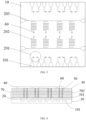
- a quantum chip structure shown in FIG. 1 is a structural diagram designed by the applicant according to the related technologies for forming six qubits 40 and corresponding signal transmission lines 20 on a surface of a two-dimensional substrate. It may be seen from the figure that the six qubits 40 occupy a few structural dimensions on the surface of the substrate, and most of surface structures are occupied by the signal transmission lines 20. In addition, due to the physical structure of the qubits 40, wiring of the signal transmission lines 20 may be limited. It is contemplated that if more bits of qubits 40 need to be integrated on the surface of the two-dimensional substrate, the integration may be very difficult due to size limitation of a chip, making it difficult to extend the quantity of qubits 40. Through research and experiments of the inventors, a novel quantum chip structure that facilitates extension of a quantity of qubits 40 is proposed.
- Some embodiments of the present application provide a quantum chip.
- FIG. 2 is a schematic structural diagram of an exemplary quantum chip not forming part of the present invention.
- a quantum chip provided in an embodiment of the present application may include: a base substrate 10 on which signal transmission lines 20 are formed; and at least one insulating substrate 30, where the at least one insulating substrate 30 is located on the base substrate 10, a qubit 40 and a through hole 50 penetrating through the insulating substrate 30 are formed on the insulating substrate 30, a metal piece 60 is formed in the through hole 50, and two ends of the metal piece 60 are electrically connected to the signal transmission lines 20 and the qubit 40, respectively.
- the base substrate 10 may include a substrate in the field of semiconductor chips, for example, a sapphire substrate, a silicon substrate, a silicon carbide substrate, or a gallium nitride substrate.
- a silicon carbide substrate is preferably selected as the base substrate 10, so that a quantum chip formed easily has a good thermal conductivity, thereby greatly reducing thermal power consumption during operation of the quantum chip, and making thermal power consumption and thermal radiation in a quantum computing system including the quantum chip reduced.
- the signal transmission lines 20 for regulating and controlling the qubit 40 are all integrated on the base substrate 10, and the qubit 40 is formed on another insulating substrate 30, so that regulation and control of the connected qubit 40 by a signal on the signal transmission lines 20 are more accurate, and a crosstalk impact on another qubit 40 may be reduced.
- a process of forming the signal transmission lines 20 on the base substrate reference may be made to a semiconductor chip fabrication process in the related technologies as follows: first, forming a metal layer on a surface of the base substrate 10 by using an evaporation method, atomic deposition method, and the like; and then performing patterning, exposing, developing, and etching on the metal layer to form desired signal transmission lines 20. A more detailed process is not described again in the embodiment of the present application.
- a layer of insulating substrate 30 for arrangement of a circuit structure of the qubit 40 is formed on the base substrate 10.
- the insulating substrate 30 may be formed on the base substrate 10 by separately processing the insulating substrate 30 and grafting the insulating substrate 30 onto the base substrate 10, or may be formed directly on the base substrate 10 by using an atomic deposition process or a sputtering process.
- the second method is used, that is, the insulating substrate 30 is formed on the base substrate 10 by using a sputtering process.
- the signal transmission lines 20 are formed on a surface of the base substrate 10, and the insulating substrate 30 formed on the base substrate 10 covers a surface of the signal transmission lines 20, so as to isolate the signal transmission lines 20 from a circuit structure of the qubit 40, thereby achieving insulation and isolation functions.
- the circuit structure of the qubit 40 may be formed on the surface of the insulating substrate 30.
- the circuit structure of the qubit 40 formed in this case is disconnected from the signal transmission lines 20.
- a through hole 50 penetrating through the insulating substrate 30 needs to be formed on the insulating substrate 30, and a metal piece 60 is filled in the through hole 50; therefore, the signal transmission lines 20 and the qubit 40 may be electrically connected by means of the metal piece 60.
- the circuit structure of the qubit 40 may be formed on the surface of the insulating substrate 30 after the through hole 50 and the metal piece 60 located in the through hole 50 are prepared on the insulating substrate 30.
- the formed circuit structure of the qubit 40 is electrically connected to one end of the metal piece 60, and the other end of the metal piece 60 is electrically connected to the signal transmission lines 20 on the base substrate 10.
- the circuit structure of the qubit 40 and the signal transmission lines 20 are electrically connected by means of the metal piece 60, so that signal transmission is implemented between the signal transmission lines 20 and the qubit 40, constructing a complete circuit structure of the qubit 40.
- the signal transmission lines 20 and the qubit 40 are respectively formed on the base substrate 10 and the insulating substrate 30, the through hole 50 penetrating through the insulating substrate 30 and the metal piece 60 located in the through hole 50 are formed, and then the signal transmission lines 20 on the base substrate 10 and the qubit 40 on the insulating substrate 30 are electrically connected by means of the metal piece 60, so that signal transmission is implemented between the signal transmission lines 20 and the qubit 40, forming a complete qubit circuit located on different layers.
- a plurality of insulating substrates 30 that are stacked may be used for forming qubits 40 located on insulating substrates 30 in different layers, thereby expanding a quantity of the qubits 40 to an enough amount. In this way, an integration degree of a quantum chip is improved.
- the signal transmission lines 20 provided in the example not forming part of the present invention include: a qubit control signal line 201 coupled to the qubit 40, where the qubit control signal line 201 is configured to regulate and control information of the qubit 40; a qubit microwave resonant cavity 202 coupled to the qubit 40, where the qubit microwave resonant cavity 202 is configured to read information of the qubit 40; and a qubit read signal line 203 coupled to the qubit microwave resonant cavity 202, where the qubit read signal line 203 is configured to read information output by the qubit microwave resonant cavity 202.
- a quantum chip running quantum computing integrates a plurality of computing units (namely, qubits 40), and each qubit 40 is a two-level system. Transition frequency and transition energy of an energy level system of each qubit 40 are both regulated and controlled by using an applied regulation signal, for example, the transition frequency of the qubit 40 is regulated and controlled by applying a direct-current bias signal and the transition energy of the qubit 40 is regulated and controlled by applying a microwave signal. Therefore, each qubit 40 needs to be provided with a corresponding qubit control signal line 201, and the qubit control signal line 201 is configured to transmit an applied regulation and control signal to the qubit 40.
- a corresponding qubit read signal line 203 further needs to be disposed to read the qubit 40. Since response sensitivity of the qubit 40 to a signal is very high, the qubit 40 cannot be read directly through the qubit read signal line 203, and need to be read indirectly by means of the qubit microwave resonant cavity 202, and then information of the qubit 40 fed back through the qubit microwave resonant cavity 202 is read through the qubit read signal line 203.
- the qubit microwave resonant cavity 202 provided in the example includes a coplanar waveguide transmission line.
- the qubit microwave resonant cavity 202 is formed on the base substrate 10 and a form of a coplanar waveguide transmission line is used, which is easy to prepare, and compared with the form of microstrip transmission lines, less crosstalk occurs between signals transmitted on the coplanar waveguide transmission lines.
- the quantum chip provided in the embodiment of the present application further includes an isolation layer 70, where the isolation layer 70 is located between the base substrate 10 and the insulating substrate 30, and the through hole 50 penetrates through the isolation layer 70.
- the embodiment of the present application provides a quantum chip structure, that is, a layer of isolation layer 70 is formed between the base substrate 10 and the insulating substrate 30.
- a layer of isolation layer 70 is formed between the base substrate 10 and the insulating substrate 30.
- the through hole 50 also needs to penetrate through the formed isolation layer 70, that is, the through hole 50 penetrates through the insulating substrate 30 and the isolation layer 70.
- the metal piece 60 is formed in the through hole 50, and two ends of the metal piece 60 are respectively electrically connected to the signal transmission lines 20 on the base substrate 10 and the qubit 40 on the insulating substrate 30. In this way, signal transmission between the signal transmission lines 20 and the qubit 40 is implemented.
- an isolation layer 70 is formed between the base substrate 10 and the insulating substrate 30, an isolation effect between the signal transmission lines 20 on the base substrate 10 and the qubit 40 on the insulating substrate 30 may be improved, so that there is less crosstalk impact of a signal transmitted on the signal transmission lines 20 on another qubit 40.
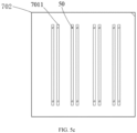
- the isolation layer 70 provided in the embodiment of the present application may include: an insulating isolation layer 701 located on the base substrate 10, where the insulating isolation layer 701 covers the signal transmission lines 20, and the through hole 50 penetrates through the insulating isolation layer 701; and a metal isolation layer 702 located on the insulating isolation layer 701, where a via hole 7011 for forming a mesh is formed in the metal isolation layer 702, and the through hole 50 is located in the via hole 7011 for forming a mesh.
- the metal isolation layer 702 is used, and the metal isolation layer 702 is disposed between the base substrate 10 and the insulating substrate 30, so that there has a good isolation effect between the signal transmission lines 20 on the base substrate 10 and the qubit 40 on the insulating substrate 30.
- a material of the metal isolation layer 702 includes one of copper, aluminum, gold, and niobium or a metal or an alloy of another material, as long as an effect of isolation can be achieved.
- copper is preferably selected, because copper has a low cost and a simple fabrication process.
- the metal isolation layer 702 not only is located on the base substrate 10, but also covers the signal transmission lines 20 and contacts the signal transmission lines 20. If the metal isolation layer 702 is directly formed on the signal transmission lines 20, a short circuit may be caused between the metal isolation layer 702 and the signal transmission lines 20. Therefore, an insulating isolation layer 701 needs to be further disposed between the metal isolation layer 702 and the signal transmission lines 20, and the insulating isolation layer 701 is configured to protect the signal transmission lines 20 from being short circuited by the metal isolation layer 702.
- the insulating substrate 30 is formed on an upper surface of the metal isolation layer 702, and because the insulating substrate 30 is made of an insulating material, the qubit 40 formed on the insulating substrate 30 is not affected.
- a material of the insulating isolation layer 701 includes one of silicon dioxide, amorphous silicon and Teflon. In a specific implementation of the present application, silicon dioxide is preferably used, because silicon dioxide has a simple fabrication process.
- the through hole 50 also needs to be formed in the insulating isolation layer 701 and the metal isolation layer 702 that are formed between the base substrate 10 and the insulating substrate 30.
- the metal isolation layer 702 is a metal isolation layer, a via hole 7011 for forming a mesh with an aperture greater than that of the through hole 50 needs to be further formed on the metal isolation layer 702.
- the via hole 7011 for forming a mesh and the through hole 50 are coaxially disposed, so that the through hole 50 is located in the via hole '7011 for forming a mesh.
- a coverage region of the through hole 50 is allowed to be located within a coverage region of the via hole 7011 for forming a mesh, so as to ensure that there is no short circuit between the metal isolation layer 702 and the metal piece 60 in the through hole 50 penetrating through the metal isolation layer 702.
- an embodiment of the present application provides a structure in which a via hole 7011 for forming a mesh is formed in a metal isolation layer 702.
- a metal layer may be first formed on an insulating isolation layer 701, and then the via hole 7011 for forming a mesh is formed by using an etching process.
- a position of the via hole 7011 for forming a mesh needs to be set based on a position of the through hole 50, so as to ensure that the through hole 50 penetrating through the insulating substrate 30, the insulating isolation layer 701, and the metal isolation layer 702 is located inside the via hole 7011 for forming a mesh.
- a coverage region of the through hole 50 is allowed to be located within a coverage area of the via hole 7011 for forming a mesh, to ensure that after the metal piece 60 in the through hole 50 electrically connects the signal transmission lines 20 on the base substrate 10 and the qubit 40 on the insulating substrate 30, there is no short circuit between the metal piece 60 and the metal isolation layer 702.
- the hole of the metal isolation layer 702 shown in FIG. 5a is a structure of the via hole 7011 for forming a mesh.
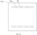
- the via hole 7011 for forming a mesh may also have a variety of hole-like structures, such as strip-shaped holes shown in FIG. 5b , FIG. 5c , and FIG. 5d , so long as a hole in the metal isolation layer 702 can surround the through hole 50, and ensure that there is no short circuit between the metal isolation layer 702 and the metal piece 60 in the through hole 50.
- the at least one insulating substrate provided in the embodiment of the present application may include a first insulating substrate 301 and a second insulating substrate 302.
- the first insulating substrate 301 is located on the base substrate 10
- a first qubit 401 and a through hole 50 are formed on the first insulating substrate 301
- the through hole 50 penetrates through the first insulating substrate 301
- a metal piece 60 is formed in the through hole 50
- two ends of the metal piece 60 are electrically connected to the signal transmission lines 20 and the first qubit 401, respectively, so as to implement signal transmission between the signal transmission lines 20 and the first qubit 401.
- the second insulating substrate 302 is located on the first insulating substrate 301, a second qubit 402 and a through hole 50 are formed on the second insulating substrate 302, the through hole 50 penetrates through the second insulating substrate 302, a metal piece 60 is formed in the through hole 50, and two ends of the metal piece 60 are electrically connected to the signal transmission lines 20 and the second qubit 402, respectively, so as to implement signal transmission between the signal transmission lines 20 and the second qubit 402.
- a structure in which a plurality of layers of insulating substrates 30 are stacked may be used, for example, when there are a plurality of qubits 40 for a superconducting quantum chip and it is difficult to integrate circuit structures of the plurality of qubits 40 on one layer of insulating substrate 30, a plurality of layers of insulating substrates 30 that are stacked may be formed, and a circuit structure of a qubit 40 may be formed on a surface of each insulating substrate 30.
- a through hole 50 penetrating through the insulating substrate 30 needs to be formed in each insulating substrate 30 in the plurality of layers of insulating substrates 30, and a metal piece 60 is formed in the through hole 50, so that all circuits of the qubits 40 on the surface of the plurality of layers of insulating substrates 30 are electrically connected to the signal transmission lines 20 on the base substrate 10 by means of the metal piece 60.
- the first insulating substrate 301 and the second insulating substrate 302 described in the embodiment of the present application are merely examples, and a third insulating substrate, a fourth insulating substrate, and more insulating substrates may be further formed on the second insulating substrate 302.
- a through hole 50 penetrating through each layer of the insulating substrate 30 needs to be formed in each layer of the insulating substrate 30 and a metal piece 60 needs to be formed in the through hole 50.
- the circuit structures of the qubits 40 may be arranged by forming a plurality of layers of stacked insulating substrates 30, an integration degree of the qubits 40 on the quantum chip may be greatly improved; and a same process is used in a fabrication process, facilitating production and fabrication.
- FIG. 7 is a diagram of a circuit structure of the first qubit 401 on a surface of the first insulating substrate 301
- FIG. 8 shows a diagram of a circuit structure of the second qubit 402 on a surface of the second insulating substrate 302, where a corresponding structural diagram of the base substrate 10 is shown in FIG. 3 .
- two through holes 50 namely, control signal line through holes 501, are formed beside the circuit structure of each of the first qubit 401 and the second qubit 402 respectively on the first insulating substrate 301 and the second insulating substrate 302.
- a metal piece 60 is formed in each of the through holes 50 for electrically connecting the qubit control signal line 201, and the metal piece 60 is configured to transmit signals for controlling transition frequency and transition energy of an energy level system of a qubit 40 to the qubit 40.
- a through hole 50 namely, a read signal line through hole 502 is formed at an end away from the structure of the qubit 40.
- the qubit 40 is electrically connected to a qubit microwave resonant cavity 202 located on the base substrate 10 by means of the metal piece 60 in the through hole 50, thereby transmitting information of the qubit 40 to the read signal line through hole 502.
- each qubit 40 is at least paired to form at least two control signal line through holes 501 and one read signal line through hole 502, and a metal piece 60 in each of the three through holes 50 is electrically connected to a corresponding qubit 40.
- the metal piece 60 provided in the embodiment of the present application fully fills the through hole 50.
- the metal piece 60 is formed in the through hole 50 for implementing electrical connection between the base substrate 10 and a circuit structure on the insulating substrate 30.
- a metal piece 60 in a shape of a metal film may be formed on the inner surface of the through hole 50 by sputtering, or a metal piece 60 in a columnar shape may be formed inside the through hole 50.
- the metal piece 60 in a columnar shape is used, so as to avoid that the formed through hole 50 and a metal layer formed by sputtering on the surface of the through hole 50 are uneven and have a high roughness, thereby affecting transmitted control signals.
- the metal piece 60 in a columnar shape may be formed by fully filling the through hole 50.
- a capacitor 420 for connecting the qubit 40 and the metal piece 60 is formed on the insulating substrate 30 provided in the embodiment of the present application, and adjacent qubits 40 are also coupled through the capacitor 420.
- the qubit 40 is coupled to the qubit microwave resonant cavity 202, and the qubit microwave resonant cavity 202 is directly electrically connected to the metal piece 60, so that a capacitor 420 is provided between the qubit 40 and the metal piece 60, and a coupling effect also exists between two adjacent qubits 40, so that a capacitor 420 of a cross shape is formed.
- a qubit 40 may include a loop superconducting circuit 410 and the capacitor 420.
- the qubit 40 on the quantum chip is a two-level system formed by a non-linear inductor and a resonant capacitor.
- the non-linear inductor is a loop superconducting circuit 410 connected in parallel, and the resonant capacitor is also formed based on the capacitor 420, that is, the capacitor is formed by both cross transmission lines in the middle connected to the loop superconducting circuit 410 and surrounding ground (corresponding "ground” on the insulating substrate 30) in FIG. 9 .
- the metal piece 60 that is in the through hole 50 and connects the qubit 40 is connected to the loop superconducting circuit 410.
- a two-level resonator system equivalent to an LC resonance (classical resonant circuit) is formed by the loop superconducting circuit 410 and the resonant capacitor, and then the two-level resonant system is regulated and controlled by receiving, through the metal piece 60 connected to the loop superconducting circuit 410, a control signal transmitted on the signal transmission lines 20 located on the base substrate 10.
- a structure of a qubit includes, but is not limited to, the structure of the loop superconducting circuit 410 and the capacitor 420 in this embodiment.
- the loop superconducting circuit 410 provided in the embodiment of the present application includes at least two superconducting Josephson junctions connected in parallel.
- the loop superconducting circuit 410 functions as the non-linear inductor in the two-level resonant system, and the loop superconducting circuit 410 is regulated and controlled by a control signal obtained by mean of the metal piece 60 and applied to the signal transmission lines 20, specifically by applying a control signal causing a change in magnetic flux.
- the loop superconducting circuit 410 is formed as a closed loop formed by at least two superconducting Josephson junctions connected in parallel, and the closed loop induces a change in the magnetic flux (the change in the magnetic flux is controlled and regulated by a bias voltage applied to the signal transmission lines 20), so that a parameter of the closed loop, namely, the loop superconducting circuit 410, is adjusted.
- a quantum chip provided in the example not forming part of the present invention further includes signal terminals 101, and the signal terminals 101 are formed on a side surface of the base substrate 10 and electrically connected to the signal transmission lines 20 in a one-to-one correspondence manner.
- the signal transmission lines 20 located on the base substrate 10 are configured to receive a regulation and control signal.
- the regulation and control signal is supplied from an external signal source, so that the signal terminals 101 need to be formed on the quantum chip to receive a control signal supplied from the external signal source and transmit the control signal to the qubit 40 through the signal transmission lines 20 and the metal piece 60.
- the signal terminals 101 are also formed on the base substrate 10 to facilitate direct electrical connection with the signal transmission lines 20.
- the signal terminals 101 are formed on the side surface of the base substrate 10, and a function thereof is similar to pins of a semiconductor chip.
- a fabrication method for a quantum chip is provided in some other implementations of the embodiment of the present application.
- FIG. 10 shows an exemplary fabrication method for a quantum chip.
- an example provides a fabrication method for a quantum chip, and the fabrication method may include the following steps.
- Step S10 Providing a base substrate 10 on which signal transmission lines 20 are formed.
- a base substrate 10 is provided, and the base substrate 10 may be a sapphire substrate, a silicon substrate, or the like.
- a superconducting metal layer is formed on a surface of the base substrate 10 by using an evaporation method, atomic deposition method, and the like; and further, a metal layer is patterned, exposed, developed, and etched to form desired signal transmission lines 20.
- Step S20 Forming at least one insulating substrate 30 on the base substrate 10, where a qubit 40 and a through hole 50 penetrating through the insulating substrate 30 are formed on the insulating substrate 30, a metal piece 60 is formed in the through hole 50, and two ends of the metal piece 60 are electrically connected to the signal transmission lines 20 and the qubit 40, respectively.
- the insulating substrate 30 is formed on the base substrate 10 by using an atomic deposition process or a sputtering process, a through hole 50 penetrating through the insulating substrate 30 is formed on the insulating substrate 30, and a metal piece 60 is formed by filling a metal in the through hole 50, so that circuit structures on both sides of the insulating substrate 30 may be electrically connected by means of the metal piece 60.
- an embodiment of the present application provides a method for forming at least one insulating substrate 30 on the base substrate 10, and the method may include:
- the present application provides a quantum chip and a fabrication method therefor, and the quantum chip includes a base substrate on which signal transmission lines are formed; and at least one insulating substrate located on the base substrate, and an isolation layer between the base substrate and the at least one insulating substrate, where a qubit and a through hole penetrating through the insulating substrate and the isolation layer are formed on the insulating substrate, a metal piece is formed in the through hole, and two ends of the metal piece are electrically connected to the signal transmission lines and the qubit, respectively, such that signal transmission between the signal transmission lines and the qubit is implemented and a qubit complete circuit located on different layers is formed , and a plurality of insulating substrates that are stacked are used for forming qubits located on insulating substrates in different layers, thereby expanding a quantity of the qubits to an enough amount. In this way, an integration degree of a quantum chip is improved.
- the quantum chip and the fabrication method therefor in the present application may be reproduced, and may be used in various industrial applications.
- a quantum chip and a fabrication method therefor in the present application may be applied to the field of quantum technologies.
Landscapes
- Engineering & Computer Science (AREA)
- General Physics & Mathematics (AREA)
- Theoretical Computer Science (AREA)
- Physics & Mathematics (AREA)
- Mathematical Analysis (AREA)
- Computing Systems (AREA)
- Evolutionary Computation (AREA)
- Condensed Matter Physics & Semiconductors (AREA)
- Computational Mathematics (AREA)
- Mathematical Optimization (AREA)
- Pure & Applied Mathematics (AREA)
- Data Mining & Analysis (AREA)
- General Engineering & Computer Science (AREA)
- Mathematical Physics (AREA)
- Software Systems (AREA)
- Artificial Intelligence (AREA)
- Manufacturing & Machinery (AREA)
- Internal Circuitry In Semiconductor Integrated Circuit Devices (AREA)
- Superconductor Devices And Manufacturing Methods Thereof (AREA)
Claims (14)
- Ein Quantenchip, der Folgendes beinhaltet:ein Basissubstrat (10), auf dem Signalübertragungskanäle (20) gebildet sind; undmindestens ein isolierendes Substrat (30), wobei sich das isolierende Substrat (30) auf dem Basisssubstrat (10) befindet, wobei ein Qubit (40) und ein Durchgangsloch (50), das durch das isolierende Substrat (30) hindurchgeht, auf dem isolierenden Substrat (30) gebildet sind, wobei ein Metallstück (60) in dem Durchgangsloch (50) gebildet ist; und zwei Enden des Metallstücks (60) mit den Signalübertragungskanälen (20) bzw. dem Qbit (40) elektrisch verbunden sind, dadurch gekennzeichnet, dass der Quantenchip ferner eine Trennschicht (70) beinhaltet, wobei sich die Trennschicht (70) zwischen dem Basissubstrat (10) und dem isolierenden Substrat (30) befindet und das Durchgangsloch (50) durch die Trennschicht (70) hindurchgeht.
- Quantenchip gemäß Anspruch 1, wobei die Signalübertragungskanäle (20) Folgendes beinhalten:einen Qubitsteuerungssignalkanal (201), der mit dem Qubit (40) gekoppelt ist, wobei der Qubit(40)-Steuerungssignalkanal konfiguriert ist, um Informationen des Qubits (40) zu steuern;einen Qubitmikrowellenresonanzhohlraum (202), der mit dem Qubit (40) gekoppelt ist,wobei der Qubitmikrowellenresonanzhohlraum (202) konfiguriert ist, um Informationen des Qubits (40) zu lesen; undeinen Qubitlesesignalkanal (203), der mit dem Qubitmikrowellenresonanzhohlraum (202) gekoppelt ist, wobei der Qubitlesesignalkanal (203) konfiguriert ist, um Informationsausgaben durch den Qubitmikrowellenresonanzhohlraum (202) zu lesen.
- Quantenchip gemäß Anspruch 2, wobei der Qubitmikrowellenresonanzhohlraum (202) einen Übertragungskanal eines koplanaren Wellenleiters beinhaltet.
- Quantenchip gemäß Anspruch 1, wobei die Trennschicht (70) Folgendes beinhaltet:eine isolierende Trennschicht (701), die sich auf dem Basissubstrat (10) befindet, wobei die isolierende Trennschicht (701) die Signalübertragungskanäle (20) bedeckt und das Durchgangsloch (10) durch die isolierende Trennschicht (701) hindurchgeht; undeine Metalltrennschicht (702), die sich auf der isolierenden Trennschicht (701) befindet,wobei ein Kontaktloch (7011) zum Bilden einer Masche auf der Metalltrennschicht (702) gebildet ist und sich das Durchgangsloch (50) in dem Kontaktloch (7011) zum Bilden einer Masche befindet.
- Quantenchip gemäß Anspruch 4, wobei eine Öffnung des Kontaktlochs (7011) zum Bilden einer Masche größer als eine Öffnung des Durchgangsloch (50) ist und das Kontaktloch (7011) zum Bilden einer Masche und das Durchgangsloch (50) koaxial angeordnet sind.
- Quantenchip gemäß einem der Ansprüche 1 bis 5, wobei das mindestens eine isolierende Substrat (30) Folgendes beinhaltet:ein erstes isolierendes Substrat (301), das sich auf dem Basissubstrat (10) befindet, wobei ein erstes Qubit (401) und ein Durchgangsloch (50), das durch das erste isolierende Substrat (301) hindurchgeht, auf dem ersten isolierenden Substrat (301) gebildet sind, ein Metallstück (60) in dem Durchgangsloch (50) gebildet ist und zwei Enden des Metallstücks (60) mit den Signalübertragungskanälen (20) bzw. dem ersten Qubit (401) elektrisch verbunden sind; undein zweites isolierendes Substrat (302), das sich auf dem ersten isolierenden Substrat (301) befindet, wobei ein zweites Qubit (402) und ein Durchgangsloch (50), das sowohl durch das zweite isolierende Substrat (302) als auch das erste isolierende Substrat (301) hindurchgeht, auf dem zweiten isolierenden Substrat (302) gebildet sind, ein Metallstück (60) in dem Durchgangsloch (50) gebildet ist und zwei Enden des Metallstücks (60) mit den Signalübertragungskanälen (20) bzw. dem zweiten Qubit (402) elektrisch verbunden sind.
- Quantenchip gemäß einem der Ansprüche 1 bis 6, wobei das Metallstück (60) das Durchgangsloch (50) vollständig füllt und konfiguriert ist, um eine elektrische Verbindung zwischen dem Basissubstrat (10) und einer Schaltungsstruktur auf dem isolierenden Substrat (30) zu implementieren.
- Quantenchip gemäß einem der Ansprüche 1 bis 7, wobei das Metallstück (60) ein Metallfilm ist, der auf einer inneren Oberfläche des Durchgangslochs (50) gebildet ist; oder das Metallstück (60) in einer säulenartigen Form innerhalb des Durchgangslochs (50) gebildet ist.
- Quantenchip gemäß einem der Ansprüche 1 bis 8, wobei ein Kondensator (420) zum Verbinden des Qubits (40) und des Metallstücks (60) auf dem isolierenden Substrat (30) gebildet ist; und benachbarte Qubits (40) durch den Kondensator (420) miteinander gekoppelt sind.
- Quantenchip gemäß Anspruch 9, wobei, wenn der Quantenchip ein supraleitender Quantenchip ist, das Qubit (40) einen supraleitenden Regelkreis (410) und den Kondensator (420) beinhaltet und das Metallstück (60), das mit dem Qubit (40) verbunden ist und sich in dem Durchgangsloch (50) befindet, mit dem supraleitenden Regelkreis (410) verbunden ist.
- Quantenchip gemäß Anspruch 10, wobei der supraleitende Regelkreis (410) mindestens zwei supraleitende Josephson-Übergänge beinhaltet, die parallel geschaltet sind.
- Quantenchip gemäß einem der Ansprüche 1 bis 11, wobei der Quantenchip ferner Signalanschlüsse (101) beinhaltet und die Signalanschlüsse (101) an einer Seitenoberfläche des Basissubstrats (10) gebildet sind und mit den Signalübertragungskanälen (10) in einer eineindeutigen Weise elektrisch verbunden sind.
- Ein Herstellungsverfahren für einen Quantenchip, das Folgendes beinhaltet:Bereitstellen (S10) eines Basissubstrats (10), auf dem Signalübertragungskanäle (20) gebildet sind; undBilden (S20) mindestens eines isolierenden Substrats (30) auf dem Basisssubstrat (10), wobei ein Qubit (40) und ein Durchgangsloch (50), das durch das isolierende Substrat (30) hindurchgeht, auf dem isolierenden Substrat (30) gebildet sind, wobei ein Metallstück (60) in dem Durchgangsloch (50) gebildet ist und zwei Enden des Metallstücks (60) mit den Signalübertragungskanälen (20) bzw. dem Qbit (40) elektrisch verbunden sind, dadurch gekennzeichnet, dass das Herstellungsverfahren ferner Folgendes beinhaltet:
Bilden einer Trennschicht (70) zwischen dem Basissubstrat (10) und dem isolierenden Substrat (30), wobei das Durchgangsloch (50) durch die Trennschicht (70) hindurchgeht. - Herstellungsverfahren gemäß Anspruch 13, wobei der Schritt des Bildens (S20) mindestens eines isolierenden Substrats (30) auf dem Basissubstrat (10), wobei ein Qubit (40) und ein Durchgangsloch (50), das durch das isolierende Substrat (30) hindurchgeht, auf dem isolierenden Substrat (30) gebildet sind, wobei ein Metallstück (60) in dem Durchgangsloch (50) gebildet ist und zwei Enden des Metallstücks (60) mit den Signalübertragungskanälen (20) bzw. dem Qbit (40) elektrisch verbunden sind, Folgendes beinhaltet:Bilden (S10) eines ersten isolierenden Substrats (301) auf dem Basissubstrat (10) und Bilden eines ersten Qubits (401) und eines Durchgangslochs (50), das durch das erste isolierende Substrat (301) hindurchgeht, auf dem ersten isolierenden Substrat (301), wobei ein Metallstück (60) in dem Durchgangsloch (50) gebildet ist und zwei Enden des Metallstücks (60) mit den Signalübertragungskanälen (20) bzw. dem ersten Qubit (401) elektrisch verbunden sind; undBilden (S20) eines zweiten isolierenden Substrats (302) auf dem ersten isolierenden Substrat (301) und Bilden eines zweiten Qubits (402) und eines Durchgangslochs (50), das sowohl durch das zweite isolierende Substrat (302) als auch das erste isolierende Substrat (301) hindurchgeht, auf dem zweiten isolierenden Substrat (302), wobei ein Metallstück (60) in dem Durchgangsloch (50) gebildet ist und zwei Enden des Metallstücks (60) mit den Signalübertragungskanälen (20) bzw. dem zweiten Qubit (402) elektrisch verbunden sind.
Applications Claiming Priority (2)
| Application Number | Priority Date | Filing Date | Title |
|---|---|---|---|
| CN202110264015.9A CN115050886B (zh) | 2021-03-09 | 2021-03-09 | 一种量子芯片及制备方法 |
| PCT/CN2022/076501 WO2022188604A1 (zh) | 2021-03-09 | 2022-02-16 | 一种量子芯片及制备方法 |
Publications (3)
| Publication Number | Publication Date |
|---|---|
| EP4220745A1 EP4220745A1 (de) | 2023-08-02 |
| EP4220745A4 EP4220745A4 (de) | 2024-05-29 |
| EP4220745B1 true EP4220745B1 (de) | 2025-04-02 |
Family
ID=83156732
Family Applications (1)
| Application Number | Title | Priority Date | Filing Date |
|---|---|---|---|
| EP22766130.3A Active EP4220745B1 (de) | 2021-03-09 | 2022-02-16 | QUANTENCHIP UND HERSTELLUNGSVERFAHREN dafür |
Country Status (4)
| Country | Link |
|---|---|
| US (1) | US20230276719A1 (de) |
| EP (1) | EP4220745B1 (de) |
| CN (1) | CN115050886B (de) |
| WO (1) | WO2022188604A1 (de) |
Families Citing this family (7)
| Publication number | Priority date | Publication date | Assignee | Title |
|---|---|---|---|---|
| CN118339566A (zh) | 2021-06-11 | 2024-07-12 | 西克公司 | 针对超导量子电路的通量偏置的系统和方法 |
| CN115496220B (zh) * | 2022-11-18 | 2023-03-24 | 材料科学姑苏实验室 | 一种量子比特芯片封装结构 |
| CN116261392B (zh) * | 2023-01-17 | 2024-09-20 | 深圳量旋科技有限公司 | 超导量子芯片及其基底、及基底的制作方法 |
| CN115955906B (zh) * | 2023-01-20 | 2025-05-30 | 深圳量旋科技有限公司 | 超导量子芯片及其基底、及基底的制作方法 |
| CN116415675B (zh) * | 2023-06-09 | 2023-09-22 | 中国科学技术大学 | 一种用于调制超导量子比特跃迁频率的系统及方法 |
| US20250309515A1 (en) * | 2024-03-28 | 2025-10-02 | International Business Machines Corporation | Loss reduction and impedance engineering for cryogenic applications |
| GB2643673A (en) * | 2024-06-13 | 2026-03-04 | Oxford Quantum Circuits Ltd | A quantum computation chip and a method of fabricating a quantum computation chip |
Family Cites Families (11)
| Publication number | Priority date | Publication date | Assignee | Title |
|---|---|---|---|---|
| US10134972B2 (en) * | 2015-07-23 | 2018-11-20 | Massachusetts Institute Of Technology | Qubit and coupler circuit structures and coupling techniques |
| WO2018052399A1 (en) * | 2016-09-13 | 2018-03-22 | Google Llc | Reducing loss in stacked quantum devices |
| AU2017404536B2 (en) * | 2017-03-13 | 2020-05-14 | Google Llc | Integrating circuit elements in a stacked quantum computing device |
| US10319896B2 (en) * | 2017-06-29 | 2019-06-11 | Intel Corporation | Shielded interconnects |
| WO2019117972A1 (en) * | 2017-12-17 | 2019-06-20 | Intel Corporation | Qubit vertical transmission line with ground vias surrounding a signal line |
| WO2019117975A1 (en) * | 2017-12-17 | 2019-06-20 | Intel Corporation | Through-silicon via integration for quantum circuits |
| WO2019117974A1 (en) * | 2017-12-17 | 2019-06-20 | Intel Corporation | Qubit vertical transmission line with a ground structure surrounding a signal line |
| WO2019117973A1 (en) * | 2017-12-17 | 2019-06-20 | Intel Corporation | Qubit vertical transmission line with two parallel ground planes |
| US10468578B2 (en) * | 2018-02-20 | 2019-11-05 | Intel Corporation | Package substrates with top superconductor layers for qubit devices |
| US10811588B2 (en) * | 2018-08-06 | 2020-10-20 | International Business Machines Corporation | Vertical dispersive readout of qubits of a lattice surface code architecture |
| CN214378496U (zh) * | 2021-03-09 | 2021-10-08 | 合肥本源量子计算科技有限责任公司 | 一种量子芯片 |
-
2021
- 2021-03-09 CN CN202110264015.9A patent/CN115050886B/zh active Active
-
2022
- 2022-02-16 WO PCT/CN2022/076501 patent/WO2022188604A1/zh not_active Ceased
- 2022-02-16 EP EP22766130.3A patent/EP4220745B1/de active Active
-
2023
- 2023-04-27 US US18/308,539 patent/US20230276719A1/en active Pending
Also Published As
| Publication number | Publication date |
|---|---|
| CN115050886B (zh) | 2024-08-16 |
| US20230276719A1 (en) | 2023-08-31 |
| EP4220745A4 (de) | 2024-05-29 |
| EP4220745A1 (de) | 2023-08-02 |
| CN115050886A (zh) | 2022-09-13 |
| WO2022188604A1 (zh) | 2022-09-15 |
Similar Documents
| Publication | Publication Date | Title |
|---|---|---|
| EP4220745B1 (de) | QUANTENCHIP UND HERSTELLUNGSVERFAHREN dafür | |
| CN214378496U (zh) | 一种量子芯片 | |
| CN109997156B (zh) | 超导量子位器件封装 | |
| US10256206B2 (en) | Qubit die attachment using preforms | |
| US10847705B2 (en) | Reducing crosstalk from flux bias lines in qubit devices | |
| US10468578B2 (en) | Package substrates with top superconductor layers for qubit devices | |
| KR102217205B1 (ko) | 적층된 양자 컴퓨팅 디바이스 내의 집적 회로 소자 | |
| US20210280676A1 (en) | Quantum dot devices | |
| EP4086965B1 (de) | Reduzierung des verlusts in gestapelten quantenvorrichtungen | |
| US10319896B2 (en) | Shielded interconnects | |
| US10756004B1 (en) | Quantum computing assemblies with through-hole dies | |
| CN110796256B (zh) | 一种量子芯片结构及制备方法 | |
| US12566988B2 (en) | Quantum computing systems with diabatic single flux quantum (SFQ) readout for superconducting quantum bits | |
| CA3198725A1 (en) | Interconnections between quantum computing module and non-quantum processing modules in quantum computing systems | |
| US20190044668A1 (en) | Quantum circuit assemblies with on-chip demultiplexers | |
| US11443223B1 (en) | Transmon qubit flip-chip structures for quantum computing devices | |
| WO2019004991A1 (en) | ASSEMBLIES OF QUANTUM CALCULATORS | |
| CN110945536A (zh) | 用于量子位的衬底设计 | |
| US12160233B2 (en) | Quantum circuit, quantum chip, and quantum computer | |
| KR20240134923A (ko) | 인터포저를 구비한 양자 컴퓨팅 장치와 그 제조 및 동작 방법, 탄탈룸 질화물을 포함하는 양자 컴퓨팅 장치 및 그 제조 방법 | |
| CN219288081U (zh) | 一种超导电路和量子芯片 | |
| CN115730666A (zh) | 一种超导量子芯片及一种量子计算机 | |
| CN115169564B (zh) | 量子比特系统及量子计算的方法 | |
| CN115496220B (zh) | 一种量子比特芯片封装结构 | |
| CN115438797A (zh) | 读取结构、量子电路及量子芯片 |
Legal Events
| Date | Code | Title | Description |
|---|---|---|---|
| STAA | Information on the status of an ep patent application or granted ep patent |
Free format text: STATUS: THE INTERNATIONAL PUBLICATION HAS BEEN MADE |
|
| PUAI | Public reference made under article 153(3) epc to a published international application that has entered the european phase |
Free format text: ORIGINAL CODE: 0009012 |
|
| STAA | Information on the status of an ep patent application or granted ep patent |
Free format text: STATUS: REQUEST FOR EXAMINATION WAS MADE |
|
| 17P | Request for examination filed |
Effective date: 20230428 |
|
| AK | Designated contracting states |
Kind code of ref document: A1 Designated state(s): AL AT BE BG CH CY CZ DE DK EE ES FI FR GB GR HR HU IE IS IT LI LT LU LV MC MK MT NL NO PL PT RO RS SE SI SK SM TR |
|
| RAP3 | Party data changed (applicant data changed or rights of an application transferred) |
Owner name: ORIGIN QUANTUM COMPUTING TECHNOLOGY (HEFEI) CO., LTD |
|
| REG | Reference to a national code |
Ref country code: DE Free format text: PREVIOUS MAIN CLASS: H01L0039220000 Ipc: H10N0060120000 Ref country code: DE Ref legal event code: R079 Ref document number: 602022012679 Country of ref document: DE Free format text: PREVIOUS MAIN CLASS: H01L0039220000 Ipc: H10N0060120000 |
|
| A4 | Supplementary search report drawn up and despatched |
Effective date: 20240430 |
|
| RIC1 | Information provided on ipc code assigned before grant |
Ipc: H10N 60/80 20230101ALI20240424BHEP Ipc: G06N 10/40 20220101ALI20240424BHEP Ipc: H10N 60/01 20230101ALI20240424BHEP Ipc: H10N 69/00 20230101ALI20240424BHEP Ipc: H10N 60/12 20230101AFI20240424BHEP |
|
| DAV | Request for validation of the european patent (deleted) | ||
| DAX | Request for extension of the european patent (deleted) | ||
| GRAP | Despatch of communication of intention to grant a patent |
Free format text: ORIGINAL CODE: EPIDOSNIGR1 |
|
| STAA | Information on the status of an ep patent application or granted ep patent |
Free format text: STATUS: GRANT OF PATENT IS INTENDED |
|
| INTG | Intention to grant announced |
Effective date: 20241028 |
|
| GRAS | Grant fee paid |
Free format text: ORIGINAL CODE: EPIDOSNIGR3 |
|
| GRAA | (expected) grant |
Free format text: ORIGINAL CODE: 0009210 |
|
| STAA | Information on the status of an ep patent application or granted ep patent |
Free format text: STATUS: THE PATENT HAS BEEN GRANTED |
|
| AK | Designated contracting states |
Kind code of ref document: B1 Designated state(s): AL AT BE BG CH CY CZ DE DK EE ES FI FR GB GR HR HU IE IS IT LI LT LU LV MC MK MT NL NO PL PT RO RS SE SI SK SM TR |
|
| REG | Reference to a national code |
Ref country code: GB Ref legal event code: FG4D |
|
| REG | Reference to a national code |
Ref country code: CH Ref legal event code: EP |
|
| REG | Reference to a national code |
Ref country code: IE Ref legal event code: FG4D |
|
| REG | Reference to a national code |
Ref country code: DE Ref legal event code: R096 Ref document number: 602022012679 Country of ref document: DE |
|
| REG | Reference to a national code |
Ref country code: NL Ref legal event code: MP Effective date: 20250402 |
|
| PG25 | Lapsed in a contracting state [announced via postgrant information from national office to epo] |
Ref country code: NL Free format text: LAPSE BECAUSE OF FAILURE TO SUBMIT A TRANSLATION OF THE DESCRIPTION OR TO PAY THE FEE WITHIN THE PRESCRIBED TIME-LIMIT Effective date: 20250402 |
|
| REG | Reference to a national code |
Ref country code: AT Ref legal event code: MK05 Ref document number: 1782626 Country of ref document: AT Kind code of ref document: T Effective date: 20250402 |
|
| PG25 | Lapsed in a contracting state [announced via postgrant information from national office to epo] |
Ref country code: ES Free format text: LAPSE BECAUSE OF FAILURE TO SUBMIT A TRANSLATION OF THE DESCRIPTION OR TO PAY THE FEE WITHIN THE PRESCRIBED TIME-LIMIT Effective date: 20250402 Ref country code: FI Free format text: LAPSE BECAUSE OF FAILURE TO SUBMIT A TRANSLATION OF THE DESCRIPTION OR TO PAY THE FEE WITHIN THE PRESCRIBED TIME-LIMIT Effective date: 20250402 Ref country code: PT Free format text: LAPSE BECAUSE OF FAILURE TO SUBMIT A TRANSLATION OF THE DESCRIPTION OR TO PAY THE FEE WITHIN THE PRESCRIBED TIME-LIMIT Effective date: 20250804 |
|
| REG | Reference to a national code |
Ref country code: LT Ref legal event code: MG9D |
|
| PG25 | Lapsed in a contracting state [announced via postgrant information from national office to epo] |
Ref country code: GR Free format text: LAPSE BECAUSE OF FAILURE TO SUBMIT A TRANSLATION OF THE DESCRIPTION OR TO PAY THE FEE WITHIN THE PRESCRIBED TIME-LIMIT Effective date: 20250703 Ref country code: NO Free format text: LAPSE BECAUSE OF FAILURE TO SUBMIT A TRANSLATION OF THE DESCRIPTION OR TO PAY THE FEE WITHIN THE PRESCRIBED TIME-LIMIT Effective date: 20250702 |
|
| PG25 | Lapsed in a contracting state [announced via postgrant information from national office to epo] |
Ref country code: PL Free format text: LAPSE BECAUSE OF FAILURE TO SUBMIT A TRANSLATION OF THE DESCRIPTION OR TO PAY THE FEE WITHIN THE PRESCRIBED TIME-LIMIT Effective date: 20250402 |
|
| PG25 | Lapsed in a contracting state [announced via postgrant information from national office to epo] |
Ref country code: BG Free format text: LAPSE BECAUSE OF FAILURE TO SUBMIT A TRANSLATION OF THE DESCRIPTION OR TO PAY THE FEE WITHIN THE PRESCRIBED TIME-LIMIT Effective date: 20250402 |
|
| PG25 | Lapsed in a contracting state [announced via postgrant information from national office to epo] |
Ref country code: HR Free format text: LAPSE BECAUSE OF FAILURE TO SUBMIT A TRANSLATION OF THE DESCRIPTION OR TO PAY THE FEE WITHIN THE PRESCRIBED TIME-LIMIT Effective date: 20250402 |
|
| PG25 | Lapsed in a contracting state [announced via postgrant information from national office to epo] |
Ref country code: AT Free format text: LAPSE BECAUSE OF FAILURE TO SUBMIT A TRANSLATION OF THE DESCRIPTION OR TO PAY THE FEE WITHIN THE PRESCRIBED TIME-LIMIT Effective date: 20250402 |
|
| PG25 | Lapsed in a contracting state [announced via postgrant information from national office to epo] |
Ref country code: RS Free format text: LAPSE BECAUSE OF FAILURE TO SUBMIT A TRANSLATION OF THE DESCRIPTION OR TO PAY THE FEE WITHIN THE PRESCRIBED TIME-LIMIT Effective date: 20250702 |
|
| PG25 | Lapsed in a contracting state [announced via postgrant information from national office to epo] |
Ref country code: IS Free format text: LAPSE BECAUSE OF FAILURE TO SUBMIT A TRANSLATION OF THE DESCRIPTION OR TO PAY THE FEE WITHIN THE PRESCRIBED TIME-LIMIT Effective date: 20250802 |
|
| PG25 | Lapsed in a contracting state [announced via postgrant information from national office to epo] |
Ref country code: LV Free format text: LAPSE BECAUSE OF FAILURE TO SUBMIT A TRANSLATION OF THE DESCRIPTION OR TO PAY THE FEE WITHIN THE PRESCRIBED TIME-LIMIT Effective date: 20250402 |
|
| REG | Reference to a national code |
Ref country code: DE Ref legal event code: R097 Ref document number: 602022012679 Country of ref document: DE |
|
| PG25 | Lapsed in a contracting state [announced via postgrant information from national office to epo] |
Ref country code: SM Free format text: LAPSE BECAUSE OF FAILURE TO SUBMIT A TRANSLATION OF THE DESCRIPTION OR TO PAY THE FEE WITHIN THE PRESCRIBED TIME-LIMIT Effective date: 20250402 Ref country code: DK Free format text: LAPSE BECAUSE OF FAILURE TO SUBMIT A TRANSLATION OF THE DESCRIPTION OR TO PAY THE FEE WITHIN THE PRESCRIBED TIME-LIMIT Effective date: 20250402 |
|
| PG25 | Lapsed in a contracting state [announced via postgrant information from national office to epo] |
Ref country code: CZ Free format text: LAPSE BECAUSE OF FAILURE TO SUBMIT A TRANSLATION OF THE DESCRIPTION OR TO PAY THE FEE WITHIN THE PRESCRIBED TIME-LIMIT Effective date: 20250402 |
|
| PG25 | Lapsed in a contracting state [announced via postgrant information from national office to epo] |
Ref country code: EE Free format text: LAPSE BECAUSE OF FAILURE TO SUBMIT A TRANSLATION OF THE DESCRIPTION OR TO PAY THE FEE WITHIN THE PRESCRIBED TIME-LIMIT Effective date: 20250402 |
|
| PG25 | Lapsed in a contracting state [announced via postgrant information from national office to epo] |
Ref country code: SK Free format text: LAPSE BECAUSE OF FAILURE TO SUBMIT A TRANSLATION OF THE DESCRIPTION OR TO PAY THE FEE WITHIN THE PRESCRIBED TIME-LIMIT Effective date: 20250402 |
|
| PG25 | Lapsed in a contracting state [announced via postgrant information from national office to epo] |
Ref country code: IT Free format text: LAPSE BECAUSE OF FAILURE TO SUBMIT A TRANSLATION OF THE DESCRIPTION OR TO PAY THE FEE WITHIN THE PRESCRIBED TIME-LIMIT Effective date: 20250402 |
|
| PLBE | No opposition filed within time limit |
Free format text: ORIGINAL CODE: 0009261 |
|
| STAA | Information on the status of an ep patent application or granted ep patent |
Free format text: STATUS: NO OPPOSITION FILED WITHIN TIME LIMIT |
|
| REG | Reference to a national code |
Ref country code: CH Ref legal event code: L10 Free format text: ST27 STATUS EVENT CODE: U-0-0-L10-L00 (AS PROVIDED BY THE NATIONAL OFFICE) Effective date: 20260211 |
|
| 26N | No opposition filed |
Effective date: 20260105 |
|
| PGFP | Annual fee paid to national office [announced via postgrant information from national office to epo] |
Ref country code: DE Payment date: 20260206 Year of fee payment: 5 |