EP4220721A1 - Solid-state imaging device and electronic apparatus - Google Patents
Solid-state imaging device and electronic apparatus Download PDFInfo
- Publication number
- EP4220721A1 EP4220721A1 EP21872283.3A EP21872283A EP4220721A1 EP 4220721 A1 EP4220721 A1 EP 4220721A1 EP 21872283 A EP21872283 A EP 21872283A EP 4220721 A1 EP4220721 A1 EP 4220721A1
- Authority
- EP
- European Patent Office
- Prior art keywords
- pixel
- semiconductor layer
- photoelectric conversion
- imaging device
- solid
- Prior art date
- Legal status (The legal status is an assumption and is not a legal conclusion. Google has not performed a legal analysis and makes no representation as to the accuracy of the status listed.)
- Pending
Links
Images
















Classifications
-
- H—ELECTRICITY
- H10—SEMICONDUCTOR DEVICES; ELECTRIC SOLID-STATE DEVICES NOT OTHERWISE PROVIDED FOR
- H10K—ORGANIC ELECTRIC SOLID-STATE DEVICES
- H10K39/00—Integrated devices, or assemblies of multiple devices, comprising at least one organic radiation-sensitive element covered by group H10K30/00
- H10K39/30—Devices controlled by radiation
- H10K39/32—Organic image sensors
-
- H—ELECTRICITY
- H10—SEMICONDUCTOR DEVICES; ELECTRIC SOLID-STATE DEVICES NOT OTHERWISE PROVIDED FOR
- H10F—INORGANIC SEMICONDUCTOR DEVICES SENSITIVE TO INFRARED RADIATION, LIGHT, ELECTROMAGNETIC RADIATION OF SHORTER WAVELENGTH OR CORPUSCULAR RADIATION
- H10F39/00—Integrated devices, or assemblies of multiple devices, comprising at least one element covered by group H10F30/00, e.g. radiation detectors comprising photodiode arrays
- H10F39/10—Integrated devices
- H10F39/12—Image sensors
- H10F39/18—Complementary metal-oxide-semiconductor [CMOS] image sensors; Photodiode array image sensors
- H10F39/182—Colour image sensors
- H10F39/1825—Multicolour image sensors having stacked structure, e.g. NPN, NPNPN or multiple quantum well [MQW] structures
-
- H—ELECTRICITY
- H10—SEMICONDUCTOR DEVICES; ELECTRIC SOLID-STATE DEVICES NOT OTHERWISE PROVIDED FOR
- H10F—INORGANIC SEMICONDUCTOR DEVICES SENSITIVE TO INFRARED RADIATION, LIGHT, ELECTROMAGNETIC RADIATION OF SHORTER WAVELENGTH OR CORPUSCULAR RADIATION
- H10F39/00—Integrated devices, or assemblies of multiple devices, comprising at least one element covered by group H10F30/00, e.g. radiation detectors comprising photodiode arrays
- H10F39/10—Integrated devices
- H10F39/12—Image sensors
- H10F39/18—Complementary metal-oxide-semiconductor [CMOS] image sensors; Photodiode array image sensors
- H10F39/184—Infrared image sensors
-
- H—ELECTRICITY
- H10—SEMICONDUCTOR DEVICES; ELECTRIC SOLID-STATE DEVICES NOT OTHERWISE PROVIDED FOR
- H10F—INORGANIC SEMICONDUCTOR DEVICES SENSITIVE TO INFRARED RADIATION, LIGHT, ELECTROMAGNETIC RADIATION OF SHORTER WAVELENGTH OR CORPUSCULAR RADIATION
- H10F39/00—Integrated devices, or assemblies of multiple devices, comprising at least one element covered by group H10F30/00, e.g. radiation detectors comprising photodiode arrays
- H10F39/10—Integrated devices
- H10F39/12—Image sensors
- H10F39/191—Photoconductor image sensors
- H10F39/192—Colour image sensors
-
- H—ELECTRICITY
- H10—SEMICONDUCTOR DEVICES; ELECTRIC SOLID-STATE DEVICES NOT OTHERWISE PROVIDED FOR
- H10F—INORGANIC SEMICONDUCTOR DEVICES SENSITIVE TO INFRARED RADIATION, LIGHT, ELECTROMAGNETIC RADIATION OF SHORTER WAVELENGTH OR CORPUSCULAR RADIATION
- H10F39/00—Integrated devices, or assemblies of multiple devices, comprising at least one element covered by group H10F30/00, e.g. radiation detectors comprising photodiode arrays
- H10F39/80—Constructional details of image sensors
- H10F39/802—Geometry or disposition of elements in pixels, e.g. address-lines or gate electrodes
-
- H—ELECTRICITY
- H10—SEMICONDUCTOR DEVICES; ELECTRIC SOLID-STATE DEVICES NOT OTHERWISE PROVIDED FOR
- H10F—INORGANIC SEMICONDUCTOR DEVICES SENSITIVE TO INFRARED RADIATION, LIGHT, ELECTROMAGNETIC RADIATION OF SHORTER WAVELENGTH OR CORPUSCULAR RADIATION
- H10F39/00—Integrated devices, or assemblies of multiple devices, comprising at least one element covered by group H10F30/00, e.g. radiation detectors comprising photodiode arrays
- H10F39/80—Constructional details of image sensors
- H10F39/802—Geometry or disposition of elements in pixels, e.g. address-lines or gate electrodes
- H10F39/8027—Geometry of the photosensitive area
-
- H—ELECTRICITY
- H10—SEMICONDUCTOR DEVICES; ELECTRIC SOLID-STATE DEVICES NOT OTHERWISE PROVIDED FOR
- H10F—INORGANIC SEMICONDUCTOR DEVICES SENSITIVE TO INFRARED RADIATION, LIGHT, ELECTROMAGNETIC RADIATION OF SHORTER WAVELENGTH OR CORPUSCULAR RADIATION
- H10F39/00—Integrated devices, or assemblies of multiple devices, comprising at least one element covered by group H10F30/00, e.g. radiation detectors comprising photodiode arrays
- H10F39/80—Constructional details of image sensors
- H10F39/803—Pixels having integrated switching, control, storage or amplification elements
- H10F39/8037—Pixels having integrated switching, control, storage or amplification elements the integrated elements comprising a transistor
-
- H—ELECTRICITY
- H10—SEMICONDUCTOR DEVICES; ELECTRIC SOLID-STATE DEVICES NOT OTHERWISE PROVIDED FOR
- H10F—INORGANIC SEMICONDUCTOR DEVICES SENSITIVE TO INFRARED RADIATION, LIGHT, ELECTROMAGNETIC RADIATION OF SHORTER WAVELENGTH OR CORPUSCULAR RADIATION
- H10F39/00—Integrated devices, or assemblies of multiple devices, comprising at least one element covered by group H10F30/00, e.g. radiation detectors comprising photodiode arrays
- H10F39/80—Constructional details of image sensors
- H10F39/805—Coatings
- H10F39/8053—Colour filters
-
- H—ELECTRICITY
- H10—SEMICONDUCTOR DEVICES; ELECTRIC SOLID-STATE DEVICES NOT OTHERWISE PROVIDED FOR
- H10F—INORGANIC SEMICONDUCTOR DEVICES SENSITIVE TO INFRARED RADIATION, LIGHT, ELECTROMAGNETIC RADIATION OF SHORTER WAVELENGTH OR CORPUSCULAR RADIATION
- H10F39/00—Integrated devices, or assemblies of multiple devices, comprising at least one element covered by group H10F30/00, e.g. radiation detectors comprising photodiode arrays
- H10F39/80—Constructional details of image sensors
- H10F39/806—Optical elements or arrangements associated with the image sensors
-
- H—ELECTRICITY
- H10—SEMICONDUCTOR DEVICES; ELECTRIC SOLID-STATE DEVICES NOT OTHERWISE PROVIDED FOR
- H10F—INORGANIC SEMICONDUCTOR DEVICES SENSITIVE TO INFRARED RADIATION, LIGHT, ELECTROMAGNETIC RADIATION OF SHORTER WAVELENGTH OR CORPUSCULAR RADIATION
- H10F39/00—Integrated devices, or assemblies of multiple devices, comprising at least one element covered by group H10F30/00, e.g. radiation detectors comprising photodiode arrays
- H10F39/80—Constructional details of image sensors
- H10F39/807—Pixel isolation structures
-
- H—ELECTRICITY
- H10—SEMICONDUCTOR DEVICES; ELECTRIC SOLID-STATE DEVICES NOT OTHERWISE PROVIDED FOR
- H10F—INORGANIC SEMICONDUCTOR DEVICES SENSITIVE TO INFRARED RADIATION, LIGHT, ELECTROMAGNETIC RADIATION OF SHORTER WAVELENGTH OR CORPUSCULAR RADIATION
- H10F39/00—Integrated devices, or assemblies of multiple devices, comprising at least one element covered by group H10F30/00, e.g. radiation detectors comprising photodiode arrays
- H10F39/80—Constructional details of image sensors
- H10F39/811—Interconnections
-
- H—ELECTRICITY
- H10—SEMICONDUCTOR DEVICES; ELECTRIC SOLID-STATE DEVICES NOT OTHERWISE PROVIDED FOR
- H10F—INORGANIC SEMICONDUCTOR DEVICES SENSITIVE TO INFRARED RADIATION, LIGHT, ELECTROMAGNETIC RADIATION OF SHORTER WAVELENGTH OR CORPUSCULAR RADIATION
- H10F39/00—Integrated devices, or assemblies of multiple devices, comprising at least one element covered by group H10F30/00, e.g. radiation detectors comprising photodiode arrays
- H10F39/80—Constructional details of image sensors
- H10F39/812—Arrangements for transferring the charges in the image sensor perpendicular to the imaging plane, e.g. buried regions used to transfer generated charges to circuitry under the photosensitive region
-
- H—ELECTRICITY
- H10—SEMICONDUCTOR DEVICES; ELECTRIC SOLID-STATE DEVICES NOT OTHERWISE PROVIDED FOR
- H10K—ORGANIC ELECTRIC SOLID-STATE DEVICES
- H10K30/00—Organic devices sensitive to infrared radiation, light, electromagnetic radiation of shorter wavelength or corpuscular radiation
- H10K30/80—Constructional details
- H10K30/81—Electrodes
-
- H—ELECTRICITY
- H10—SEMICONDUCTOR DEVICES; ELECTRIC SOLID-STATE DEVICES NOT OTHERWISE PROVIDED FOR
- H10K—ORGANIC ELECTRIC SOLID-STATE DEVICES
- H10K39/00—Integrated devices, or assemblies of multiple devices, comprising at least one organic radiation-sensitive element covered by group H10K30/00
- H10K39/601—Assemblies of multiple devices comprising at least one organic radiation-sensitive element
-
- H—ELECTRICITY
- H10—SEMICONDUCTOR DEVICES; ELECTRIC SOLID-STATE DEVICES NOT OTHERWISE PROVIDED FOR
- H10F—INORGANIC SEMICONDUCTOR DEVICES SENSITIVE TO INFRARED RADIATION, LIGHT, ELECTROMAGNETIC RADIATION OF SHORTER WAVELENGTH OR CORPUSCULAR RADIATION
- H10F39/00—Integrated devices, or assemblies of multiple devices, comprising at least one element covered by group H10F30/00, e.g. radiation detectors comprising photodiode arrays
- H10F39/10—Integrated devices
- H10F39/12—Image sensors
- H10F39/199—Back-illuminated image sensors
Definitions
- the present disclosure relates to a solid-state imaging device and an electronic apparatus.
- Patent Literature 1 proposes, as a method for solving false colors, a stacked-type solid-state imaging device in which photoelectric conversion regions that photoelectrically convert light of respective wavelengths of green, blue, and red are stacked in the longitudinal direction of the same pixel, and the green photoelectric conversion region is constituted by an organic photoelectric conversion film.
- Patent Literature 2 proposes a structure in which charges generated by photoelectric conversion and accumulated on the upper side of the accumulation electrode are transferred in the longitudinal direction to a collection electrode installed below the accumulation electrode.
- the present disclosure proposes a solid-state imaging device and an electronic apparatus capable of improving quantum efficiency.
- a solid-state imaging device includes: a plurality of pixels arranged in a matrix, wherein each of the pixels includes a first semiconductor layer, a photoelectric conversion section disposed on the first semiconductor layer on a side of a first surface, an accumulation electrode disposed on the first semiconductor layer close to a side of a second surface on a side opposite to the first surface, a wiring extending from the second surface of the first semiconductor layer, a floating diffusion region connected to the first semiconductor layer via the wiring, and a first gate electrode disposed close to the wiring.
- CMOS complementary metal-oxide semiconductor
- EVS a solid-state imaging device
- an electronic apparatus an electronic apparatus
- a recognition system a recognition system
- CMOS complementary metal-oxide semiconductor
- the technology according to the present embodiment can be applied to various sensors including a photoelectric conversion element, such as a charge-coupled device (CCD) image sensor, a time-of-flight (ToF) sensor, and a synchronous type or an asynchronous type event visio sensor (EVS).
- CCD charge-coupled device
- ToF time-of-flight
- EVS synchronous type or an asynchronous type event visio sensor
- the CMOS image sensor may be an image sensor created by applying or partially using a CMOS process.
- FIG. 1 is a schematic diagram depicting a schematic configuration example of an electronic apparatus according to the present embodiment
- FIG. 2 is a block diagram depicting a schematic configuration example of a distance measuring device using an electronic apparatus according to the present embodiment.
- an electronic apparatus 1 includes a laser light source 1010, an irradiation lens 1030, an imaging lens 1040, an image sensor 100, and a system control unit 1050.
- the laser light source 1010 includes, for example, a vertical cavity surface emitting laser (VCSEL) 1012 and a light source driving unit 1011 that drives the VCSEL 1012.
- VCSEL vertical cavity surface emitting laser
- the present invention is not limited to the VCSEL 1012, and various light sources such as a light emitting diode (LED) may be used.
- the laser light source 1010 may be any of a point light source, a surface light source, and a line light source. In the case of a surface light source or a line light source, the laser light source 1010 may have, for example, a configuration in which a plurality of point light sources (for example, VCSELs) is arranged one-dimensionally or two-dimensionally.
- the laser light source 1010 may emit light of a wavelength band different from the wavelength band of visible light, such as infrared (IR) light, for example.
- IR infrared
- the irradiation lens 1030 is disposed on an emission surface side of the laser light source 1010, and converts light emitted from the laser light source 1010 into irradiation light having a predetermined divergence angle.
- the imaging lens 1040 is disposed on the light receiving surface side of the image sensor 100, and forms an image by incident light on the light receiving surface of the image sensor 100.
- the incident light can also include reflected light emitted from the laser light source 1010 and reflected by a subject 901.
- the image sensor 100 includes, for example, a light receiving unit 1022 in which a plurality of pixels is arranged in a two-dimensional lattice shape, and a sensor control unit 1021 that drives the light receiving unit 1022 to generate image data, as depicted in FIG. 2 .
- the pixels disposed in the light receiving unit 1022 may include, for example, a pixel that detects light in a wavelength band of visible light, a pixel that detects light in a wavelength band other than visible light, for example, light in a wavelength band of infrared light, and the like.
- a pixel that detects light in a wavelength band other than visible light may be a pixel (for an image sensor) for generating image data of light in a wavelength band other than visible light, a pixel (for a ToF sensor) for measuring a distance to an object, or a pixel (for EVS) for detecting a luminance change.
- image data all data read out from each pixel of the light receiving unit 1022 and generated is referred to as image data.
- the system control unit 1050 includes, for example, a processor (CPU), and drives the VCSEL 1012 via the light source driving unit 1011.
- the system control unit 1050 acquires image data by controlling the image sensor 100.
- the system control unit 1050 may acquire image data obtained by detecting reflected light of irradiation light emitted from the laser light source 1010 by controlling the image sensor 100 in synchronization with control of the laser light source 1010.
- the irradiation light emitted from the laser light source 1010 is projected onto the subject (also referred to as a measurement target or an object) 901 through the irradiation lens 1030.
- the projected light is reflected by the subject 901.
- the light reflected by the subject 901 is incident on the image sensor 100 through the imaging lens 1040.
- the light receiving unit 1022 in the image sensor 100 receives the reflected light reflected by the subject 901 and generates image data.
- the image data generated by the image sensor 100 is supplied to an application processor 1100 of the electronic apparatus 1.
- the application processor 1100 can execute various types of processing such as recognition processing and arithmetic processing on the image data input from the image sensor 100.
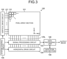
- FIG. 3 is a block diagram depicting a schematic configuration example of an image sensor in the present embodiment.
- the image sensor 100 includes, for example, a pixel array section 101, a vertical drive circuit 102, a signal processing circuit 103, a horizontal drive circuit 104, a system control circuit 105, a data processing unit 108, and a data storage section 109.
- the vertical drive circuit 102, the signal processing circuit 103, the horizontal drive circuit 104, the system control circuit 105, the data processing unit 108, and the data storage section 109 are also referred to as peripheral circuits.
- the pixel array section 101 has a configuration in which pixels (hereinafter, referred to as a unit pixel) 110 having photoelectric conversion elements that generate and accumulate charges according to the amount of received light are disposed in a row direction and a column direction, that is, in a two-dimensional lattice shape (hereinafter, also referred to as a matrix).
- the row direction refers to an arrangement direction of pixels in a pixel row (lateral direction in drawings)
- the column direction refers to an arrangement direction of pixels in a pixel column (longitudinal direction in drawings).
- a pixel drive line LD is wired along the row direction for each pixel row, and a vertical signal line VSL is wired along the column direction for each pixel column with respect to the matrix-like pixel array.
- the pixel drive line LD transmits a drive signal for driving when a signal is read out from a pixel.
- the pixel drive lines LD are depicted as wiring lines one by one, but are not limited to wiring lines one by one.
- One end of the pixel drive line LD is connected to an output terminal corresponding to each row of the vertical drive circuit 102.
- the vertical drive circuit 102 includes a shift register, an address decoder, and the like, and drives each pixel of the pixel array section 101 simultaneously for all pixels or in units of rows. That is, the vertical drive circuit 102 includes a driving unit that controls the operation of each pixel of the pixel array section 101 together with the system control circuit 105 that controls the vertical drive circuit 102. Although a specific configuration of the vertical drive circuit 102 is not depicted, the vertical drive circuit 102 generally includes two scanning systems of a readout scanning system and a sweep scanning system.
- the readout scanning system In order to read out a signal from the each pixel of the unit pixel 110, the readout scanning system sequentially selects and scans each pixel of the unit pixel 110 of the pixel array section 101 in units of rows.
- the signal read out from each pixel of the unit pixel 110 is an analog signal.
- the sweep scanning system performs sweep scanning on a read row on which read scanning is performed by the readout scanning system prior to the readout scanning by an exposure time.
- the electronic shutter operation refers to an operation of discarding charges of the photoelectric conversion element and newly starting exposure (starting accumulation of charges).
- the signal read out by the readout operation by the readout scanning system corresponds to the amount of light received after the immediately preceding readout operation or electronic shutter operation. Then, a period from the readout timing by the immediately preceding readout operation or the sweep timing by the electronic shutter operation to the readout timing by the current readout operation is the charge accumulation period (exposure period) in each pixel of the unit pixel 110.
- the signal output from each unit pixel 110 of the pixel row selectively scanned by the vertical drive circuit 102 is input to the signal processing circuit 103 through each of the vertical signal line VSL for each pixel column.
- the signal processing circuit 103 performs predetermined signal processing on the signal output from each unit pixel of the selected row through the vertical signal line VSL for each pixel column of the pixel array section 101, and temporarily holds the pixel signal after the signal processing.
- the signal processing circuit 103 performs at least noise removal processing, for example, correlated double sampling (CDS) processing as signal processing and double data sampling (DDS). For example, by the CDS processing, fixed pattern noise unique to pixels such as reset noise and threshold variation of the amplification transistor in the pixel is removed.
- the signal processing circuit 103 also has, for example, an analog-digital (AD) conversion function, converts an analog pixel signal read out from the photoelectric conversion element into a digital signal, and outputs the digital signal.
- AD analog-digital
- the horizontal drive circuit 104 includes a shift register, an address decoder, and the like, and sequentially selects a readout circuit (hereinafter, referred to as a pixel circuit) corresponding to the pixel column of the signal processing circuit 103.
- a readout circuit hereinafter, referred to as a pixel circuit
- the system control circuit 105 includes a timing generator that generates various timing signals and the like, and performs drive control of the vertical drive circuit 102, the signal processing circuit 103, and the horizontal drive circuit 104 based on various timings generated by the timing generator.
- the data processing unit 108 has at least an arithmetic processing function, and performs various types of signal processing such as arithmetic processing on the pixel signal output from the signal processing circuit 103.
- the data storage section 109 temporarily stores data necessary for signal processing in the data processing unit 108.
- image data output from the data processing unit 108 may be subjected to predetermined processing in the application processor 1100 and the like in the electronic apparatus 1 equipped with the image sensor 100, or may be transmitted to the outside via a predetermined network, for example.
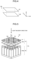
- FIG. 4 is a diagram depicting a stacked structure example of the image sensor according to the present embodiment.
- the image sensor 100 has a stack structure in which a light receiving chip 121 and a circuit chip 122 are vertically stacked.
- the light receiving chip 121 may be, for example, a semiconductor chip including a pixel array section 101 in which a plurality of unit pixels 110 are arranged in a matrix
- the circuit chip 122 may be, for example, a semiconductor chip including a peripheral circuit and the like in FIG. 3 .
- the bonding surfaces are planarized and both are bonded to each other by an electronic force.
- the present invention is not limited to this, and for example, so-called Cu-Cu bonding in which copper (Cu) electrode pads formed on the bonding surfaces are bonded to each other, bump bonding, and the like can also be used.
- the light receiving chip 121 and the circuit chip 122 are electrically connected via a connecting section such as a through-silicon via (TSV) penetrating the semiconductor substrate, for example.
- TSV through-silicon via
- a so-called twin TSV method in which two TSVs, that is, a TSV provided in the light receiving chip 121 and a TSV provided from the light receiving chip 121 to the circuit chip 122 are connected by an outer surface of the chip
- a so-called shared TSV method in which both are connected by a TSV penetrating from the light receiving chip 121 to the circuit chip 122, and the like can be adopted.
- the unit pixel 110 includes a pixel (hereinafter, also referred to as an RGB pixel 10) that detects each color component in the three primary colors of RGB and a pixel (hereinafter, also referred to as an IR pixel 20) that detects infrared (IR) light
- a pixel hereinafter, also referred to as an RGB pixel 10.
- IR pixel 20 a pixel that detects infrared (IR) light
- FIG. 5 is a schematic diagram depicting a schematic configuration example of a pixel array section according to the present embodiment.
- the pixel array section 101 has a configuration in which the unit pixels 110 having a structure in which the unit pixels 110 including the RGB pixels 10 and the IR pixels 20 are arranged along the light incident direction are arranged in a two-dimensional lattice shape. That is, in the present embodiment, the RGB pixels 10 and the IR pixels 20 are positioned in the direction vertical to the arrangement direction (plane direction) of the unit pixels 110, and the light transmitted through the RGB pixels 10 positioned on the upstream side in the optical path of the incident light is configured to be incident on the IR pixels 20 positioned on the downstream side of the RGB pixels 10.
- a photoelectric conversion section PD2 of the IR pixel 20 is disposed on the surface side opposite to the incident surface of the incident light in a photoelectric conversion section PD1 of the RGB pixel 10.
- the optical axes of the incident light of the RGB pixel 10 and the IR pixel 20 arranged along the light incident direction coincide or substantially coincide with each other.
- both the photoelectric conversion section PD1 and the photoelectric conversion section PD2 may be made of a semiconductor material, both the photoelectric conversion section PD1 and the photoelectric conversion section PD2 may be made of an organic material, or the photoelectric conversion section PD1 may be made of a semiconductor material and the photoelectric conversion section PD2 may be made of an organic material.
- at least one of the photoelectric conversion section PD1 and the photoelectric conversion section PD2 may be made of a photoelectric conversion material different from the organic material and the semiconductor material.
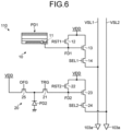
- FIG. 6 is a circuit diagram depicting a schematic configuration example of a unit pixel according to the present embodiment.
- the unit pixel 110 includes one RGB pixel 10 and one IR pixel 20.
- the RGB pixel 10 includes, for example, the photoelectric conversion section PD1, a transfer gate 11, a floating diffusion region FD1, a reset transistor 12, an amplification transistor 13, and a selection transistor 14.
- a selection control line included in the pixel drive line LD is connected to the gate of the selection transistor 14, a reset control line included in the pixel drive line LD is connected to the gate of the reset transistor 12, and a transfer control line included in the pixel drive line LD is connected to an accumulation electrode (see an accumulation electrode 37 in FIG. 8 to be described later) to be described later of the transfer gate 11.
- a vertical signal line VSL1 having one end connected to the signal processing circuit 103 is connected to the drain of the amplification transistor 13 via the selection transistor 14.
- the reset transistor 12, the amplification transistor 13, and the selection transistor 14 are also collectively referred to as a pixel circuit.
- the pixel circuit may include the floating diffusion region FD1 and/or the transfer gate 11.
- the photoelectric conversion section PD1 is made of, for example, an organic material, and photoelectrically converts incident light.
- the transfer gate 11 transfers the charges generated in the photoelectric conversion section PD1.
- the floating diffusion region FD1 accumulates the charges transferred by the transfer gate 11.
- the amplification transistor 13 causes a pixel signal having a voltage value corresponding to the charges accumulated in the floating diffusion region FD1 to appear in the vertical signal line VSL1.
- the reset transistor 12 releases the charges accumulated in the floating diffusion region FD1.
- the selection transistor 14 selects the RGB pixel 10 to be read out.
- the anode of the photoelectric conversion section PD1 is grounded, and the cathode is connected to the transfer gate 11.
- the accumulation electrode 37 is disposed close. At the time of exposure, a voltage for collecting charges generated in the photoelectric conversion section PD1 to a semiconductor layer 35 near the accumulation electrode 37 is applied to the accumulation electrode 37 via the transfer control line. At the time of reading, a voltage for causing charges collected in the semiconductor layer 35 near the accumulation electrode 37 to flow out through a readout electrode 36 is applied to the accumulation electrode 37 through the transfer control line.
- the charges flowing out through the readout electrode 36 are accumulated in the floating diffusion region FD1 including a wiring structure connecting the readout electrode 36, the source of the reset transistor 12, and the gate of the amplification transistor 13.
- the drain of the reset transistor 12 may be connected to, for example, a power supply voltage VDD or a power supply line to which a reset voltage lower than the power supply voltage VDD is supplied.
- the source of the amplification transistor 13 may be connected to a power supply line via, for example, a constant current circuit (not depicted) and the like.
- the drain of the amplification transistor 13 is connected to the source of the selection transistor 14, and the drain of the selection transistor 14 is connected to the vertical signal line VSL1.
- the floating diffusion region FD1 converts the accumulated charges into a voltage of a voltage value corresponding to the charge amount.
- the floating diffusion region FD1 may be, for example, a ground capacity.
- the present invention is not limited to this, and the floating diffusion region FD1 may be a capacity and the like added by intentionally connecting a capacitor and the like to a node where the drain of the transfer gate 11, the source of the reset transistor 12, and the gate of the amplification transistor 13 are connected.
- the vertical signal line VSL1 is connected to an analog-to-digital (AD) conversion circuit 103a provided for each column (that is, for each vertical signal line VSL1) in the signal processing circuit 103.
- the AD conversion circuit 103a includes, for example, a comparator and a counter, and converts an analog pixel signal into a digital pixel signal by comparing a reference voltage such as a single slope or a ramp shape input from an external reference voltage generation circuit (digital-to-analog converter (DAC)) with the pixel signal appearing in the vertical signal line VSL1.
- DAC digital-to-analog converter
- the AD conversion circuit 103a may include, for example, a correlated double sampling (CDS) circuit and the like, and may be configured to be able to reduce kTC noise and the like.
- CDS correlated double sampling
- the IR pixel 20 includes, for example, the photoelectric conversion section PD2, a transfer transistor 21, a floating diffusion region FD2, a reset transistor 22, an amplification transistor 23, a selection transistor 24, and a discharge transistor 25. That is, in the IR pixel 20, the transfer gate 11 in the RGB pixel 10 is replaced with the transfer transistor 21, and the discharge transistor 25 is added.
- connection relationship among the floating diffusion region FD2, the reset transistor 22, and the amplification transistor 23 with respect to the transfer transistor 21 may be similar to the connection relationship among the floating diffusion region FD1, the reset transistor 12, and the amplification transistor 13 with respect to the transfer gate 11 in the RGB pixel 10.
- connection relationship among the amplification transistor 23, the selection transistor 24, and a vertical signal line VSL2 may be similar to the connection relationship among the amplification transistor 13, the selection transistor 14, and the vertical signal line VSL1 in the RGB pixel 10.
- the source of the transfer transistor 21 is connected to, for example, the cathode of the photoelectric conversion section PD2, and the drain is connected to the floating diffusion region FD2.
- the transfer control line included in the pixel drive line LD is connected to the gate of the transfer transistor 21.
- the source of the discharge transistor 25 may be connected to, for example, the cathode of the photoelectric conversion section PD2, and the drain may be connected to the power supply voltage VDD or a power supply line to which a reset voltage lower than the power supply voltage VDD is supplied.
- the discharge control line included in the pixel drive line LD is connected to the gate of the discharge transistor 25.
- the reset transistor 22, the amplification transistor 23, and the selection transistor 24 are also collectively referred to as a pixel circuit.
- the pixel circuit may include one or more of the floating diffusion region FD2, the transfer transistor 21, and the discharge transistor 25.
- the photoelectric conversion section PD2 is made of, for example, a semiconductor material, and photoelectrically converts incident light.
- the transfer transistor 21 transfers the charges generated in the photoelectric conversion section PD2.
- the floating diffusion region FD2 accumulates the charges transferred by the transfer transistor 21.
- the amplification transistor 23 causes a pixel signal having a voltage value corresponding to the charges accumulated in the floating diffusion region FD2 to appear in the vertical signal line VSL2.
- the reset transistor 22 releases the charges accumulated in the floating diffusion region FD2.
- the selection transistor 24 selects the IR pixel 20 to be read out.
- the anode of the photoelectric conversion section PD2 is grounded, and the cathode is connected to the transfer transistor 21.
- the drain of the transfer transistor 21 is connected to the source of the reset transistor 22 and the gate of the amplification transistor 23, and a wiring structure connecting these components constitutes the floating diffusion region FD2.
- the charges flowing out from the photoelectric conversion section PD2 via the transfer transistor 21 are accumulated in the floating diffusion region FD2.
- the floating diffusion region FD2 converts the accumulated charges into a voltage of a voltage value corresponding to the charge amount.
- the floating diffusion region FD2 may be, for example, a ground capacity.
- the present invention is not limited to this, and the floating diffusion region FD2 may be a capacity and the like added by intentionally connecting a capacitor and the like to a node where the drain of the transfer transistor 21, the source of the reset transistor 22, and the gate of the amplification transistor 23 are connected.
- the discharge transistor 25 is turned on when discharging the charges accumulated in the photoelectric conversion section PD2 and resetting the photoelectric conversion section PD2. As a result, the charges accumulated in the photoelectric conversion section PD2 flow out to the power supply line via the discharge transistor 25, and the photoelectric conversion section PD2 is reset to an unexposed state.
- the vertical signal line VSL2 is connected to the AD conversion circuit 103a provided for each column (that is, for each vertical signal line VSL2) in an IR signal processing circuit 103B
- FIG. 7 is a circuit diagram depicting a schematic configuration example of a unit pixel according to a modification of the present embodiment. As depicted in FIG. 7 , in the present modification, an RGB pixel 10A in each unit pixel 110 further includes a memory MEM and a transfer transistor 15.
- the memory MEM is connected to the transfer gate 11 and temporarily holds the charges flowing out from the photoelectric conversion section PD1.
- the source of the transfer transistor 15 is connected to the memory MEM, and the drain is connected to the floating diffusion region FD1.
- the gate of the transfer transistor 15 is connected to a transfer control line which is one of the pixel drive lines LD, and transfers the charges held in the memory MEM to the floating diffusion region FD1 under the control of the vertical drive circuit 102.
- the transfer gates 11 of all the RGB pixels 10 in the pixel array section 101 are simultaneously turned on.
- the charges generated in the photoelectric conversion section PD1 of each RGB pixel 10 during the same period are transferred to and held in the memory MEM of each RGB pixel 10.
- the readout of the pixel signal based on the charges held in the memory MEM may be similar to the so-called rolling shutter type readout drive.
- FIG. 8 is a cross-sectional diagram depicting a cross-sectional structure example of the image sensor according to the present embodiment.
- a cross-sectional structure example will be described focusing on a semiconductor chip in which the photoelectric conversion sections PD1 and PD2 in the unit pixel 110 are formed.
- a so-called back surface irradiation type cross-sectional structure in which the light incident surface is on the back surface side (opposite side to the element formation surface) of a semiconductor substrate 50 is exemplified, but the present invention is not limited to this, and a so-called front surface irradiation type cross-sectional structure in which the light incident surface is on the front surface side (element formation surface side) of the semiconductor substrate 50 may be used.
- an organic material is used for the photoelectric conversion section PD1 of the RGB pixel 10
- a semiconductor material also referred to as an inorganic material
- the photoelectric conversion material of each of the photoelectric conversion sections PD1 and PD2 may be used as the photoelectric conversion material of each of the photoelectric conversion sections PD1 and PD2.
- the image sensor 100 may have a cross-sectional structure in which the photoelectric conversion section PD1 and the photoelectric conversion section PD2 are built in the same semiconductor substrate 50, may have a cross-sectional structure in which a semiconductor substrate in which the photoelectric conversion section PD1 is built and a semiconductor substrate in which the photoelectric conversion section PD2 is built are bonded, or may have a cross-sectional structure in which one of the photoelectric conversion sections PD1 and PD2 is built in the semiconductor substrate 50 and the other is built in a semiconductor layer formed on the back surface or the front surface of the semiconductor substrate 50.
- the present embodiment has a structure in which the photoelectric conversion section PD2 of the IR pixel 20 is formed on the semiconductor substrate 50, and the photoelectric conversion section PD1 of the RGB pixel 10 is provided on the back surface side (opposite side to an element formation surface) of the semiconductor substrate 50.
- the back surface of the semiconductor substrate 50 is positioned on the upper side in the plane of the drawing, and the front surface is positioned on the lower side.
- a semiconductor material such as silicon (Si) may be used.
- the semiconductor material is not limited to this, and various semiconductor materials including compound semiconductors such as GaAs, InGaAs, InP, AlGaAs, InGaP, AlGaInP, and InGaAsP may be used.
- the photoelectric conversion section PD1 of the RGB pixel 10 is provided on the back surface side of the semiconductor substrate 50 with an insulating layer 53 sandwiched between.
- the photoelectric conversion section PD1 includes, for example, a photoelectric conversion film 34 made of an organic material, and a transparent electrode 33 and the semiconductor layer 35 disposed to sandwich the photoelectric conversion film 34.
- the transparent electrode 33 provided on the upper side hereinafter, the upper side in the plane of the drawing is an upper surface side, and the lower side is a lower surface side
- the semiconductor layer 35 provided on the lower surface side functions as a cathode of the photoelectric conversion section PD1.
- the semiconductor layer 35 functioning as a cathode is electrically connected to the readout electrode 36 formed in an insulating layer 53.
- the readout electrode 36 is electrically drawn out to the front surface (lower surface) side of the semiconductor substrate 50 by being connected to wirings 61, 62, 63, and 64 penetrating the insulating layer 53 and the semiconductor substrate 50.
- the wiring 64 is electrically connected to the floating diffusion region FD1 depicted in FIG. 6 .
- the accumulation electrode 37 is provided on the lower surface side of the semiconductor layer 35 functioning as a cathode with the insulating layer 53 sandwiched between.
- the accumulation electrode 37 is connected to the transfer control line in a pixel drive line LD1. As described above, at the time of exposure, a voltage for collecting charges generated in the photoelectric conversion section PD1 to the semiconductor layer 35 near the accumulation electrode 37 is applied, and at the time of readout, a voltage for causing charges collected in the semiconductor layer 35 near the accumulation electrode 37 to flow out via the readout electrode 36 is applied.
- the readout electrode 36 and the accumulation electrode 37 may be transparent conductive films.
- a transparent conductive film such as indium tin oxide (ITO) or zinc oxide (IZO) may be used for the transparent electrode 33, the readout electrode 36, and the accumulation electrode 37.
- ITO indium tin oxide
- IZO zinc oxide
- the present invention is not limited to this, and various conductive films may be used as long as the photoelectric conversion section PD2 is a conductive film capable of transmitting light in a wavelength band to be detected.
- the semiconductor layer 35 for example, a transparent semiconductor layer such as IGZO may be used.
- IGZO a transparent semiconductor layer
- the present invention is not limited to this, and various semiconductor layers may be used as long as the photoelectric conversion section PD2 is a semiconductor layer capable of transmitting light in a wavelength band to be detected.
- the insulating layer 53 for example, an insulating film such as a silicon oxide film (SiO 2 ) or a silicon nitride film (SiN) may be used.
- a silicon oxide film (SiO 2 ) or a silicon nitride film (SiN) may be used.
- the present invention is not limited to this, and various insulating films may be used as long as the photoelectric conversion section PD2 is an insulating film capable of transmitting light in a wavelength band to be detected.
- a color filter 31 is provided on the upper surface side of the transparent electrode 33 functioning as an anode with a sealing film 32 sandwiched between.
- the sealing film 32 is made of, for example, an insulating material such as silicon nitride (SiN), and may include atoms of aluminum (Al), titanium (Ti), and the like in order to prevent the atoms from diffusing from the transparent electrode 33.
- a color filter 31 that selectively transmits light of a specific wavelength component is provided for one RGB pixel 10.
- the color filter 31 may be omitted.
- the photoelectric conversion section PD2 of the IR pixel 20 includes, for example, a p-type semiconductor region 43 formed in a p-well region 42 in the semiconductor substrate 50 and an n-type semiconductor region 44 formed in the vicinity of the center of the p-type semiconductor region 43.
- the n-type semiconductor region 44 functions as, for example, a charge accumulation region that accumulates charges (electrons) generated by photoelectric conversion
- the p-type semiconductor region 43 functions as a region that forms a potential gradient for collecting the charges generated by photoelectric conversion into the n-type semiconductor region 44.
- an IR filter 41 that selectively transmits IR light is disposed on the light incident surface side of the photoelectric conversion section PD2.
- the IR filter 41 may be disposed, for example, in the insulating layer 53 provided on the back surface side of the semiconductor substrate 50.
- a fine uneven structure is provided on the light incident surface of the semiconductor substrate 50 in order to suppress reflection of incident light (IR light in this example).
- This uneven structure may be a structure called a moth-eye structure, or may be an uneven structure having a size and a pitch different from those of the moth-eye structure.
- a longitudinal transistor 45 functioning as the transfer transistor 21 is provided on the front surface (lower surface in the plane of the drawing) side of the semiconductor substrate 50, that is, the element formation surface side.
- the gate electrode of the longitudinal transistor 45 reaches the n-type semiconductor region 44 from the surface of the semiconductor substrate 50, and is connected to the vertical drive circuit 102 via wirings 65 and 66 (a part of the transfer control line of a pixel drive line LD2) formed in an interlayer insulating film 56.
- the charges flowing out via the longitudinal transistor 45 are accumulated in the floating diffusion region FD2.
- the floating diffusion region FD2 is connected to the source of the reset transistor 22 and the gate of the amplification transistor 23 via wirings (not depicted) formed in the interlayer insulating film 56.
- the floating diffusion region FD2, the reset transistor 22, the amplification transistor 23, and the selection transistor 24 may be provided on the element formation surface of the semiconductor substrate 50, or may be provided on a semiconductor substrate different from the semiconductor substrate 50.
- an image signal based on light having a wavelength component corresponding to green may be generated in an upstream side pixel (corresponding to the RGB pixel 10), and an image signal based on light having a wavelength component corresponding to red and an image signal based on light having a wavelength component corresponding to blue may be generated in a downstream side pixel (corresponding to the IR pixel 20).
- a material that selectively absorbs a wavelength component corresponding to green is used for the photoelectric conversion film 34, and instead of the IR filter 41, a color filter that selectively transmits a wavelength component corresponding to red and a color filter that selectively transmits a wavelength component corresponding to blue can be arranged in a matrix. Furthermore, in this configuration, the color filter 31 can be omitted. With this configuration, the light receiving area of the pixel that detects the wavelength component of each of the three primary colors of RGB (which may be the three primary colors of CMY and the like) constituting the color image can be expanded, in a manner that the S/N ratio can be improved due to an increase in quantum efficiency.
- RGB which may be the three primary colors of CMY and the like
- the semiconductor substrate 50 is provided with a pixel isolation section 54 that electrically isolates the plurality of unit pixels 110 from each other, and the photoelectric conversion section PD2 is provided in each region partitioned by the pixel isolation section 54.
- the pixel isolation section 54 has, for example, a lattice shape interposed between the plurality of unit pixels 110, and each photoelectric conversion section PD2 is formed in each region partitioned by the pixel isolation section 54.
- a reflection film that reflects light such as tungsten (W) or aluminum (Al) may be used.
- W tungsten
- Al aluminum
- the incident light entering the photoelectric conversion section PD2 can be reflected by the pixel isolation section 54, in a manner that the optical path length of the incident light in the photoelectric conversion section PD2 can be increased.
- the pixel isolation section 54 has a light reflection structure, it is possible to reduce leakage of light to adjacent pixels, and thus, it is also possible to further improve image quality, distance measurement accuracy, and the like.
- the configuration in which the pixel isolation section 54 has the light reflection structure is not limited to the configuration using the reflection film, and can be realized, for example, by using a material having a refractive index different from that of the semiconductor substrate 50 for the pixel isolation section 54.
- a fixed charge film 55 is provided between the semiconductor substrate 50 and the pixel isolation section 54.
- the fixed charge film 55 is formed using, for example, a high dielectric having a negative fixed charge in a manner that a positive charge (hole) accumulation region is formed at an interface portion with the semiconductor substrate 50 and generation of a dark current is suppressed. Since the fixed charge film 55 is formed to have a negative fixed charge, an electric field is applied to the interface with a semiconductor substrate 138 by the negative fixed charge, and a positive charge (hole) accumulation region is formed.
- the fixed charge film 55 can be formed of, for example, a hafnium oxide film (HfO 2 film).
- the fixed charge film 55 can be formed to contain at least one of oxides such as hafnium, zirconium, aluminum, tantalum, titanium, magnesium, yttrium, and lanthanoid elements, for example.
- FIG. 8 depicts a case where the pixel isolation section 54 has a so-called full trench isolation (FTI) structure reaching from the front surface to the back surface of the semiconductor substrate 50, but is not limited to this.
- FTI full trench isolation
- various element isolation structures such as a so-called deep trench isolation (DTI) structure in which the pixel isolation section 54 is formed from the back surface or the front surface of the semiconductor substrate 50 to the vicinity of the middle of the semiconductor substrate 50 can be adopted.
- DTI deep trench isolation
- a planarization film 52 made of a silicon oxide film, a silicon nitride film, and the like is provided on the upper surface of the color filter 31.
- the upper surface of the planarization film 52 is planarized by, for example, chemical mechanical polishing (CMP), and an on-chip lens 51 for each unit pixel 110 is provided on the planarized upper surface.
- CMP chemical mechanical polishing
- the on-chip lens 51 of each unit pixel 110 has such a curvature that incident light is collected in the photoelectric conversion sections PD1 and PD2.
- the positional relationship among the on-chip lens 51, the color filter 31, the IR filter 41, and the photoelectric conversion section PD2 in each unit pixel 110 may be adjusted according to, for example, the distance (image height) from the center of the pixel array section 101 (pupil correction).
- a light shielding film for preventing obliquely incident light from leaking into the adjacent pixel may be provided.
- the light shielding film can be positioned above the pixel isolation section 54 provided inside the semiconductor substrate 50 (upstream side in the optical path of the incident light).
- the position of the light shielding film may be adjusted according to, for example, the distance (image height) from the center of the pixel array section 101.
- Such a light shielding film may be provided, for example, in the sealing film 32 or the planarization film 52.
- a light shielding material such as aluminum (Al) or tungsten (W) may be used as a material of the light shielding film.
- the layer structure of the photoelectric conversion film 34 in a case where an organic semiconductor is used as the material of the photoelectric conversion film 34, the layer structure of the photoelectric conversion film 34 can have the following structure. However, in the case of the stacked structure, the stacking order can be appropriately changed.
- examples of the p-type organic semiconductor include a naphthalene derivative, an anthracene derivative, a phenanthrene derivative, a pyrene derivative, a perylene derivative, a tetracene derivative, a pentacene derivative, a quinacridone derivative, a thiophene derivative, a thienothiophene derivative, a benzothiophene derivative, a benzothienobenzothiophene derivative, a triallylamine derivative, a carbazole derivative, a perylene derivative, a picene derivative, a chrysene derivative, a fluoranthene derivative, a phthalocyanine derivative, a subphthalocyanine derivative, a subporphyrazine derivative, a metal complex having a heterocyclic compound as a ligand, a polythiophene derivative, a polybenzothiadiazole derivative, a polyfluorene derivative, and the like.
- n-type organic semiconductor examples include fullerene and a fullerene derivative ⁇ for example, fullerene such as C60, C70, and C74 (higher fullerenes, endohedral fullerenes, etc.), or a fullerene derivative (for example, fullerene fluoride, PCBM fullerene compound, fullerene multimer, and the like)>, an organic semiconductor having a larger (deeper) HOMO and LUMO than a p-type organic semiconductor, and a transparent inorganic metal oxide.
- fullerene and a fullerene derivative for example, fullerene such as C60, C70, and C74 (higher fullerenes, endohedral fullerenes, etc.), or a fullerene derivative (for example, fullerene fluoride, PCBM fullerene compound, fullerene multimer, and the like)>, an organic semiconductor having a larger (deeper) HOMO and
- n-type organic semiconductor examples include an organic molecule, an organometallic complex, and a subphthalocyanine derivative having a part of the molecular skeleton containing heterocyclic compounds containing a nitrogen atom, an oxygen atom, and a sulfur atom, such as pyridine derivatives, pyrazine derivatives, pyrimidine derivatives, triazine derivatives, quinoline derivatives, quinoxaline derivatives, isoquinoline derivatives, acridine derivatives, phenazine derivatives, phenanthroline derivatives, tetrazole derivatives, pyrazole derivatives, imidazole derivatives, thiazole derivatives, oxazole derivatives, imidazole derivatives, benzimidazole derivatives, benzotriazole derivatives, benzoxazole derivatives, benzoxazole derivatives, carbazole derivatives, benzofuran derivatives, dibenzofuran derivatives, subporphyrazine derivatives, polypheny
- Halogen atom as group and the like contained in fullerene derivative the following derivatives can be mentioned: linear, branched, or cyclic alkyl or phenyl group; group having linear or condensed aromatic compound; group having halide; partial fluoroalkyl group; perfluoroalkyl group; silylalkyl group; silyl alkoxy group; arylsilyl group; arylsulfanyl group; alkylsulfanyl group; arylsulfonyl group; alkylsulfonyl group; aryl sulfide group; alkyl sulfide group; amino group; alkylamino group; arylamino group; hydroxy group; alkoxy group; acylamino group; acyloxy group; carbonyl group; carboxy group; carboxamide group; carboalkoxy group; acyl group; sulfonyl group; cyano group; nitro group; group having chalcogenide
- the film thickness of the photoelectric conversion film 34 made of the organic material as described above is not limited to the following value, but may be, for example, 1 ⁇ 10 -8 m (meter) to 5 ⁇ 10 -7 m, preferably 2.5 ⁇ 10 -8 m to 3 ⁇ 10 -7 m, more preferably 2.5 ⁇ 10 -8 m to 2 ⁇ 10 -7 m, and still more preferably 1 ⁇ 10 -7 m to 1.8 ⁇ 10 -7 m.
- the organic semiconductor is often classified into a p-type and an n-type, but the p-type means that holes are easily transported, and the n-type means that electrons are easily transported, and the organic semiconductor is not limited to the interpretation that it has holes or electrons as a majority carrier of thermal excitation like the inorganic semiconductor.
- Examples of a material constituting the photoelectric conversion film 34 that photoelectrically converts light having a green wavelength include a rhodamine dye, a melacyanine dye, a quinacridone derivative, and a subphthalocyanine dye (subphthalocyanine derivative).
- examples of a material constituting the photoelectric conversion film 34 that photoelectrically converts blue light include a coumaric acid dye, tris-8-hydroxyquinoline aluminum (Alq3), a melacyanine dye, and the like.
- examples of a material constituting the photoelectric conversion film 34 that photoelectrically converts red light include a phthalocyanine dye and a subphthalocyanine dye (subphthalocyanine derivative).
- the photoelectric conversion film 34 a panchromatic photosensitive organic photoelectric conversion film that is sensitive to substantially all visible light from the ultraviolet region to the red region can be used.
- a material having a large band gap value for example, a value of a band gap of 3.0 eV (electron volt) or more
- a material having higher mobility than the material constituting the photoelectric conversion film 34 is preferably used.
- Specific examples include oxide semiconductor materials such as IGZO, transition metal dichalcogenides, silicon carbides, diamond, graphene, carbon nanotubes, and organic semiconductor materials such as fused polycyclic hydrocarbon compounds and fused heterocyclic compounds.
- the charges generated in the photoelectric conversion film 34 are electrons
- a material having an ionization potential larger than the ionization potential of the material constituting the photoelectric conversion film 34 can be used as the material constituting the semiconductor layer 35.
- the charge is a hole
- a material having an electron affinity smaller than the electron affinity of the material constituting the photoelectric conversion film 34 can be used as the material constituting the semiconductor layer 35.
- the impurity concentration in the material constituting the semiconductor layer 35 is preferably 1 ⁇ 10 18 cm -3 or less.
- the photoelectric conversion film 34 and the semiconductor layer 35 can be made of the same material as long as the photoelectric conversion performance and the mobility performance can be satisfied.
- a transparent material is desirably used as a material of each of the transparent electrode 33, the readout electrode 36, the semiconductor layer 35, and the accumulation electrode 37.
- a material made of Al-Nd (alloy of aluminum and neodymium) or ASC (alloy of aluminum, samarium, and copper) can be used.
- the band gap energy of the transparent conductive material is desirably 2.5 eV or more, and preferably 3.1 eV or more.
- the transparent electrode 33, the readout electrode 36, and the accumulation electrode 37 are transparent electrodes
- examples of the transparent conductive material constituting them include conductive metal oxides.
- indium oxide, indium-tin oxide (indium tin oxide (ITO), Sn-doped In 2 O 3 , crystalline ITO, and amorphous ITO are included
- indium-zinc oxide (IZO) obtained by adding indium as a dopant to zinc oxide
- indium-gallium oxide (IGO) obtained by adding indium as a dopant to gallium oxide
- indium-gallium-zinc oxide (IGZO (In-GaZnO 4 )) obtained by adding indium and gallium as dopants to zinc oxide
- indium-tin-zinc oxide (ITZO) obtained by adding indium and tin as dopants to zinc oxide
- IFO F-doped In 2 O 3
- tin oxide (SnO 2 ) tin oxide
- SnO 2 tin oxide
- ATO Sb-doped SnOz
- FTO F-doped SnOz
- zinc oxide including ZnO doped with
- a transparent electrode using gallium oxide, titanium oxide, niobium oxide, nickel oxide, and the like as a parent layer can also be exemplified.
- the thickness of the transparent electrode may be 2 ⁇ 10 -8 m to 2 ⁇ 10 -7 m, preferably 3 ⁇ 10 -8 m to 1 ⁇ 10 -7 m.
- each unit pixel 110 may include N (N is an integer of 1 or more) RGB pixels 10 and M (M is an integer of 1 or more) IR pixels 20.
- N RGB pixels 10 may share a part of the pixel circuit
- M IR pixels 20 may share a part of the pixel circuit.
- FIG. 9 is a schematic diagram depicting a schematic configuration example of a unit pixel according to a modification of the present embodiment.
- a unit pixel 110A has a structure in which one IR pixel 20 is disposed in the light incident direction with respect to four RGB pixels 10 arranged in two rows and two columns. That is, in the present modification, one IR pixel 20 for four RGB pixels 10 positioned in the direction vertical to the arrangement direction (plane direction) of the unit pixels 110A, and the light transmitted through four RGB pixels 10 positioned on the upstream side in the optical path of the incident light is configured to be incident on one IR pixel 20 positioned on the downstream side of four RGB pixels 10. Therefore, in the present modification, the optical axes of the incident light of the unit array of the Bayer array including four RGB pixels 10 and the IR pixel 20 coincide or substantially coincide with each other.
- FIG. 10 is a circuit diagram depicting a schematic configuration example of a unit pixel according to a modification of the present embodiment.
- the unit pixel 110A includes the plurality of RGB pixels 10-1 to 10-N (in FIG. 10 , N is 4) and one IR pixel 20.
- one pixel circuit reset transistor 12, floating diffusion region FD1, amplification transistor 13, and selection transistor 14
- the plurality of RGB pixels 10-1 to 10-N shares a pixel circuit including the reset transistor 12, the floating diffusion region FD1, the amplification transistor 13, and the selection transistor 14. That is, in the present modification, the plurality of photoelectric conversion sections PD1 and the transfer gate 11 are connected to the common floating diffusion region FD1.
- FIG. 11 is a cross-sectional diagram depicting a cross-sectional structure example of an image sensor according to a modification of the present embodiment.
- each unit pixel 110A includes four RGB pixels 10 arranged in two rows and two columns and one IR pixel 20 will be described as an example.
- a cross-sectional structure example will be described focusing on a semiconductor chip in which the photoelectric conversion sections PD1 and PD2 in the unit pixel 110A are formed.
- structures similar to the cross-sectional structure of the image sensor 100 described with reference to FIG. 8 are cited, and redundant description is omitted.
- the on-chip lens 51, the color filter 31, and the accumulation electrode 37 are divided into four in two rows and two columns (however, two out of four are depicted in FIG. 11 .), configuring four RGB pixels 10.
- the four RGB pixels 10 in each unit pixel 210 may constitute a basic array of the Bayer array.
- the unit pixel 110 (or the unit pixel 110A, and the same applies hereinafter) having the basic configuration as described above, a configuration for increasing the quantum efficiency will be described with some examples.
- the photoelectric conversion section includes an organic photoelectric conversion film (in this example, the RGB pixel 10)
- illustration and description of the pixel in which the photoelectric conversion section includes a semiconductor in the present example, the IR pixel 20
- the cross-sectional structure of the RGB pixel 10 a configuration above the color filter 31 and a configuration below the readout electrode 36 will not be depicted and described.
- the RGB pixel 10 is also simply referred to as a pixel 10.
- the readout electrode 36 electrically connected to the floating diffusion region FD1 will be described as a part of the floating diffusion region FD1.
- the charge generated by the photoelectric conversion of the photoelectric conversion film 34 may be a positive charge (that is, a hole).
- the structure and effect described in each example may be similar to other examples if not specifically mentioned.
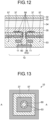
- FIG. 12 is a vertical cross-sectional diagram depicting a cross-sectional structure of a pixel according to the first example of the present embodiment.
- FIG. 13 is a horizontal cross-sectional diagram depicting an A-A cross section in FIG. 12 .
- the term “vertical” means vertical to the element formation surface of the semiconductor substrate 50
- the term “horizontal” means horizontal to the element formation surface.
- a part of the semiconductor layer 35 positioned immediately below the photoelectric conversion film 34 protrudes to the opposite side to the photoelectric conversion film 34 and is connected to the readout electrode 36.
- this protruding portion is referred to as a semiconductor wiring 60.
- the accumulation electrode 37 having the center is opened is disposed to surround the semiconductor wiring 60.
- the accumulation electrode 37 and the semiconductor wiring 60 are electrically isolated from each other with the insulating layer 53 interposed between.
- the transfer gate 11 is disposed on the side of the readout electrode 36 of the semiconductor wiring 60. Similarly to the accumulation electrode 37, the gate electrode of the transfer gate 11 has a shape having the center is opened, and is disposed to surround the semiconductor wiring 60. The gate electrode of the transfer gate 11 and the semiconductor wiring 60 are electrically isolated from each other with the insulating layer 53 interposed between. Note that, in the following description, the gate electrode of the transfer gate 11 may be simply referred to as the transfer gate 11 for simplification.
- the accumulation electrode 37 and the transfer gate 11 disposed with respect to the semiconductor wiring 60 may be divided for each pixel 10.
- a drive signal (also referred to as a control voltage) for lowering the potential in the semiconductor layer 35 near the accumulation electrode 37 is applied from the vertical drive circuit 102 to the accumulation electrode 37 during the exposure period.
- a drive signal for lowering the potential in the semiconductor layer 35 near the accumulation electrode 37 is applied from the vertical drive circuit 102 to the accumulation electrode 37 during the exposure period. Therefore, charges 58 generated in the photoelectric conversion film 34 and entering the semiconductor layer 35 are accumulated in a region near the accumulation electrode 37 in the semiconductor layer 35.
- a shield electrode (ASE) 57 is disposed to surround the periphery of the accumulation electrode (SLD) 37 of each pixel 10.
- the shield electrode 57 is connected to the vertical drive circuit 102 via a wiring (not depicted) which is one of the pixel drive lines LD.
- the vertical drive circuit 102 applies a drive signal to the shield electrode 57 to form a potential barrier in the semiconductor layer 35 positioned between the adjacent pixels 10.
- FIG. 13 a case where the horizontal cross section of the semiconductor wiring 60 and the opening shape of the accumulation electrode 37 and the transfer gate 11 are circular has been exemplified.
- the horizontal cross section and the opening shape may be changed to various shapes such as a polygon such as a quadrangle and a regular octagon and an ellipse. The same applies to other examples to be described later.
- FIG. 16 is a vertical cross-sectional diagram depicting a cross-sectional structure of a pixel according to the second example of the present embodiment.
- the pixel 10 according to the second example has a structure in which the transfer gate 11 is disposed inside the accumulation electrode 37 in a cross-sectional structure similar to that of the pixel 10 according to the first example described above with reference to FIG. 12 . That is, in the second example, the opening of the accumulation electrode 37 is enlarged in diameter, and the transfer gate 11 is disposed on the same surface as the accumulation electrode 37.
- the length of the semiconductor wiring 60 can be shortened, the height of the image sensor 100 can be reduced, and the size of the image sensor can be reduced.
- FIG. 17 is a vertical cross-sectional diagram depicting a cross-sectional structure of a pixel according to the third example of the present embodiment.
- the pixel 10 according to the third example has a tapered shape in which the semiconductor wiring 60 becomes thinner toward the readout electrode 36 in a cross-sectional structure similar to that of the pixel 10 according to the first example described above with reference to FIG. 12 .
- the diameter of the semiconductor wiring 60 on the side of the semiconductor layer 35 is increased, the charges accumulated in the semiconductor layer 35 can be smoothly transferred to the side of the readout electrode 36.
- the diameter of the semiconductor wiring 60 on the side of the readout electrode 36 is reduced, the contact area with the readout electrode 36 is reduced, in a manner that the readout electrode 36 can be reduced.
- FIG. 18 is a vertical cross-sectional diagram depicting a cross-sectional structure of a pixel according to the fourth example of the present embodiment.
- the pixel 10 according to the fourth example has a structure in which the readout electrode 36 (and the floating diffusion region FD) is shared between adjacent pixels 10 in a cross-sectional structure similar to that of the pixel 10 according to the first example described above with reference to FIG. 12 .
- the readout electrode 36 and the floating diffusion region FD are shared and the transfer of the charges from each pixel 10 to the floating diffusion region FD can be controlled using the transfer gate 11, it is possible to switch between reading for each pixel 10 and simultaneous reading from the plurality of pixels 10.
- FIG. 19 is a vertical cross-sectional diagram depicting a cross-sectional structure of a pixel according to the fifth example of the present embodiment.
- FIG. 20 is a horizontal cross-sectional diagram depicting a B-B cross section in FIG. 19 . Note that FIG. 19 depicts a configuration above the color filter 31 for convenience of description.
- the pixel 10 according to the fifth example has a structure in which one on-chip lens 51 is provided for a plurality of (two in this example) pixels 10 in a cross-sectional structure similar to that of the pixel 10 according to the first example described above with reference to FIG. 12 .
- FIG. 21 is a vertical cross-sectional diagram depicting a cross-sectional structure of a pixel according to the sixth example of the present embodiment.
- the pixel 10 according to the sixth example has a structure in which a memory electrode 16 and the transfer transistor 15 constituting the memory MEM are sequentially disposed between the transfer gate 11 and the readout electrode 36 in a cross-sectional structure similar to that of the pixel 10 according to the first example described above with reference to FIG. 12 .
- the transfer transistor 15 is disposed on the side of the semiconductor wiring 60 closest to the readout electrode 36. Similarly to the accumulation electrode 37, the gate electrode of the transfer transistor 15 has a shape having the center is opened, and is disposed to surround the semiconductor wiring 60. The gate electrode of the transfer transistor 15 and the semiconductor wiring 60 are electrically isolated from each other with the insulating layer 53 interposed between. Note that, in the following description, the gate electrode of the transfer transistor 15 may be simply referred to as the transfer transistor 15 for simplification.
- the memory electrode 16 is disposed between the transfer gate 11 and the transfer transistor 15. In addition, similarly to the accumulation electrode 37, the memory electrode 16 has a shape having the center is opened, and is disposed to surround the semiconductor wiring 60.
- the charges transferred from the semiconductor layer 35 via the transfer gate 11 can be temporarily held in the region near the memory electrode 16 in the semiconductor wiring 60.
- global shutter method readout drive becomes possible.
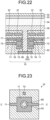
- FIG. 22 is a vertical cross-sectional diagram depicting a cross-sectional structure of a pixel according to the seventh example of the present embodiment.
- FIG. 23 is a horizontal cross-sectional diagram depicting a C-C cross section in FIG. 22 .
- the transfer gates 11 in all the pixels 10 are simultaneously driven. Therefore, as depicted in FIGS. 22 and 23 , the transfer gates 11 of all the pixels 10 in the pixel array section 101 may be coupled by wirings 71. Similarly, the memory electrodes 16 of all the pixels 10 in the pixel array section 101 may also be coupled by the wirings 72. Note that the accumulation electrodes 37 of all the pixels 10 in the pixel array section 101 may also be coupled to each other via wirings 73.
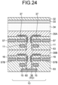
- FIG. 24 is a vertical cross-sectional diagram depicting a cross-sectional structure of a pixel according to the eighth example of the present embodiment.
- the pixel 10 according to the eighth example has a structure in which the semiconductor layer 35 is divided into two layers of a first semiconductor layer 35A and a second semiconductor layer 35B in a cross-sectional structure similar to that of the pixel 10 according to the sixth example described above with reference to FIG. 21 .
- the insulating layer 53 is interposed between the first semiconductor layer 35A and the second semiconductor layer 35B.
- the semiconductor wiring 60 penetrates through the first semiconductor layer 35A to the second semiconductor layer 35B and reaches the readout electrode 36.
- the accumulation electrode 37, the transfer gate 11, and the shield electrode 57 are disposed in the insulating layer 53 between the first semiconductor layer 35A and the second semiconductor layer 35B.
- the memory electrode 16 and the transfer transistor 15 are disposed in the insulating layer 53 between the second semiconductor layer 35B and the readout electrode 36. More specifically, the memory electrode 16 is disposed on the side of the second semiconductor layer 35B in the semiconductor wiring 60 between the second semiconductor layer 35B and the readout electrode 36, and the gate electrode of the transfer transistor 15 is disposed on the side of the readout electrode 36 in the semiconductor wiring 60 between the second semiconductor layer 35B and the readout electrode 36.
- a shield electrode 57B similar to the shield electrode 57 is provided between the memory electrodes 16 of the adjacent pixels 10.
- the shield electrode 57B is connected to the vertical drive circuit 102 via a wiring (not depicted) which is one of the pixel drive lines LD.
- the vertical drive circuit 102 applies a drive signal to the shield electrode 57 to form a potential barrier in the second semiconductor layer 35B positioned between the adjacent pixels 10.
- a drive example of the global shutter method will be described. Note that, in the present example, a drive example of the pixel 10 described in the sixth example with reference to FIG. 21 will be described, but the present invention is not limited to this, and can be similarly applied to other examples in which global shutter method drive (hereinafter, referred to as global shutter drive) is possible.
- global shutter drive global shutter method drive
- FIG. 25 is a vertical cross-sectional diagram depicting a cross-sectional structure of a pixel according to the ninth example of the present embodiment. As depicted in FIG. 25 , in the global shutter drive according to the ninth example, the exposure operation is not executed in the other pixel 10 while one pixel 10 of two adjacent pixels 10a and 10b executes the exposure operation. Note that each of the two pixels 10a and 10b may have a configuration similar to that of the pixel 10 described above.
- the accumulation electrode 37 of the pixel 10b is turned on, and the accumulation electrode 37 of the pixel 10a is turned off.
- the shield electrode 57 positioned between the two pixels 10a and 10b is turned off.
- the transfer gate 11 and the transfer transistor 15 of the pixel 10a, and the transfer gate 11, the memory electrode 16, and the transfer transistor 15 of the pixel 10b are turned off, and the memory electrode 16 of the pixel 10a is turned on.
- the ON state of the accumulation electrode 37, the shield electrode 57, and the memory electrode 16 refers to a state in which a drive signal is supplied from the vertical drive circuit 102 to each electrode, and the OFF state refers to a state in which a drive signal is not supplied from the vertical drive circuit 102.
- the charges 58 generated in the photoelectric conversion film 34 corresponding to the photoelectric conversion section PD1 of each of the pixels 10a and 10b are attracted to the accumulation electrode 37 of the pixel 10b.
- the charges 58 generated in the photoelectric conversion film 34 are accumulated in the semiconductor layer 35 near the accumulation electrode 37 in the pixel 10b.
- the outflow destination of the charges 58 overflowing from the semiconductor layer 35 near the accumulation electrode 37 in the pixel 10b may be the floating diffusion region FD connected to the readout electrode 36 of the pixel 10b.
- the charges 59 accumulated in the semiconductor layer 35 near the accumulation electrode 37 in the previous frame are held in the memory MEM.
- the charges 59 accumulated in the memory MEM are sequentially read out by the readout operation for the pixel 10a executed in parallel during the exposure of the pixel 10b, and are used for generation of a pixel signal.
- FIG. 26 is a vertical cross-sectional diagram depicting a cross-sectional structure of a pixel according to the 10th example of the present embodiment.
- the shield electrode 57 positioned between the two pixels 10a and 10b forming a pair is turned off.
- the shield electrode 57 between the two pixels 10a and 10b forming a pair is omitted.
- FIG. 27 is a vertical cross-sectional diagram depicting a cross-sectional structure of a pixel according to the 11th example of the present embodiment.
- the readout electrodes 36 and the floating diffusion regions FD of the two pixels 10a and 10b forming a pair are made common.
- global shutter drive can be realized by the driving described in the ninth example.
- FIG. 28 is a vertical cross-sectional diagram depicting a cross-sectional structure example of the pixel according to the 12th example of the present embodiment.
- the semiconductor layer 35 (including the first semiconductor layer 35A and the second semiconductor layer 35B described in the eighth example) in each of the examples described above and below may include two layers of a first layer 35a and a second layer 35b.
- the second layer 35b is provided, for example, on a surface of the semiconductor layer 35 in contact with the insulating layer 53.
- the second layer 35b may be a film provided for the purpose of reducing the interface trap level formed between the insulating layer 53 and the first layer 35a.
- a material constituting each of the first layer 35a and the second layer 35b for example, the same material as the semiconductor layer 35 described above may be used.
- the first layer 35a and the second layer 35b may have different properties depending on, for example, a difference in composition and the like.
- the interface trap level formed between the insulating layer 53 and the first layer 35a is reduced, in a manner that the afterimage generated between the frames can be reduced.
- the color filter 31 may be disposed on the side of the light incident surface (the side of the on-chip lens 51) with respect to the photoelectric conversion film 34 as depicted in FIG. 29 , or may be disposed on the side (the side of the circuit chip 122 (not depicted)) opposite to the light incident surface with respect to the photoelectric conversion film 34 as depicted in FIG. 30 .
- the color filter 31 may be disposed, for example, in the insulating layer 53 as depicted in FIG. 30 .
- the base pixel 10 is not limited to the pixel 10 according to the first example, and may be a pixel 10 according to another example.
- the material of the fixed charge film can be formed to contain a hafnium oxide film (HfO 2 film) or at least one of oxides such as hafnium, zirconium, aluminum, tantalum, titanium, magnesium, yttrium, and lanthanoid elements, for example.
- FIG. 31 is a vertical cross-sectional diagram depicting a cross-sectional structure of the pixel according to the 14th example of the present embodiment.
- FIG. 32 is a horizontal cross-sectional diagram depicting a D-D cross section in FIG. 31 .
- the shield charge film 67 may include a fixed charge film having the same polarity as the charges generated in the photoelectric conversion film 34.
- the shield charge film 67 is disposed on the same surface as the surface on which the accumulation electrode 37 is disposed. Note that the shield charge film 67 may be in contact with the side surface of the accumulation electrode 37 or may be separated from the side surface of the accumulation electrode 37.
- the configuration for driving the shield electrode 57 can be omitted, it is possible to reduce the size by omitting the shield electrode 57 and the pixel drive line LD for driving the shield electrode 57. Furthermore, in 14th example, since it is not necessary to separate the accumulation electrode 37 from the shield charge film 67, the accumulation electrode 37 can be enlarged. As a result, charges can be efficiently collected by the semiconductor layer 35 near the accumulation electrode 37, in a manner that further improvement in quantum efficiency can be expected.
- FIG. 33 is a vertical cross-sectional diagram depicting a cross-sectional structure of the pixel according to the 15th example of the present embodiment.
- the shield charge film 67 may be disposed between a surface of the insulating layer 53 on which the upper surface of the accumulation electrode 37 is disposed and the lower surface of the semiconductor layer 35 (other than the semiconductor wiring 60), which is a boundary portion between the adjacent pixels 10.
- the region around the opening in the shield charge film 67 may overlap the outer peripheral portion of the accumulation electrode 37 in the vertical direction.
- FIG. 34 is a vertical cross-sectional diagram depicting a cross-sectional structure of the pixel according to the 16th example of the present embodiment.
- the shield charge film 67 may be disposed in the lower layer portion of the semiconductor layer 35, that is, a region in contact with the insulating layer 53 in the semiconductor layer 35, which is a boundary portion between the adjacent pixels 10. At that time, the region around the opening in the shield charge film 67 may overlap the outer peripheral portion of the accumulation electrode 37 in the vertical direction.
- FIG. 35 is a vertical cross-sectional diagram depicting a cross-sectional structure of the pixel according to the 17th example of the present embodiment.
- the shield charge film 67 may be disposed at a boundary portion between the adjacent pixels 10 to replace the semiconductor layer 35 in this portion. At that time, the region around the opening in the shield charge film 67 may overlap the outer peripheral portion of the accumulation electrode 37 in the vertical direction.
- FIG. 36 is a vertical cross-sectional diagram depicting a cross-sectional structure of the pixel according to the 18th example of the present embodiment.
- the shield charge film 67 may be disposed in the lower layer portion of the photoelectric conversion film 34, that is, a region in contact with the semiconductor layer 35 in the photoelectric conversion film 34, which is a boundary portion between the adjacent pixels 10 At that time, the region around the opening in the shield charge film 67 may overlap the outer peripheral portion of the accumulation electrode 37 in the vertical direction.
- FIG. 37 is a vertical cross-sectional diagram depicting a cross-sectional structure of the pixel according to the 19th example of the present embodiment.
- the shield charge film 67 may be disposed at a boundary portion between the adjacent pixels 10 to replace the photoelectric conversion film 34 in this portion.
- the region around the opening in the shield charge film 67 may overlap the outer peripheral portion of the accumulation electrode 37 in the vertical direction.
- FIGS. 38 and 39 are vertical cross-sectional diagrams depicting a cross-sectional structure of the pixel according to the 20th example of the present embodiment.
- the shield charge film 67 may be disposed below the lower surface of the accumulation electrode 37 in the insulating layer 53 (on the side of the readout electrode 36), which is a boundary portion between the adjacent pixels 10.
- the region around the opening in the shield charge film 67 may overlap the outer peripheral portion of the accumulation electrode 37 in the vertical direction.
- the region around the opening in the shield charge film 67 and the outer peripheral portion of the accumulation electrode 37 may be in contact with each other as depicted in FIG. 38 , or may be separated from each other in the vertical direction as depicted in FIG. 39 .
- a drive example of the pixel 10 that does not include the memory MEM for global shutter drive will be described.
- the method of driving the pixel 10 according to the first example described above with reference to FIG. 12 is exemplified, but the driving method is not limited to the first example, and a similar driving method can be applied to the pixel 10 according to another example.
- FIG. 40 is a vertical cross-sectional diagram depicting a cross-sectional structure example of the pixel cited for describing the first drive example.
- the cross-sectional structure of the pixel 10 depicted in FIG. 40 may be similar to the cross-sectional structure of the pixel 10 according to the first example described above with reference to FIG. 12 .
- FIGS. 41 to 43 are band diagrams depicting a potential for each driving step along the E-E surface in FIG. 40 . Note that, in FIGS. 41 to 43 , the vertical axis represents the potential, and the horizontal axis represents the position along the E-E surface. In addition, in FIGS.
- a region (also referred to as a gate region) of the semiconductor wiring 60 having potential controlled by the transfer gate 11 is denoted as 'TG'
- a region (also referred to as an accumulation region) of the semiconductor layer 35 having potential controlled by the accumulation electrode 37 is denoted as 'ASE'
- a region (also referred to as a shield region) of the semiconductor layer 35 having potential controlled by the shield electrode 57 is denoted as 'SLD'.
- the transfer gate 11 is turned off (OFF), and the accumulation electrode 37 is turned on (ON).
- the potential of an accumulation region ASE is lowered, and a high potential barrier is formed in a gate region TG.
- the charges 58 generated in the photoelectric conversion film 34 and entering the semiconductor layer 35 are accumulated in the accumulation region ASE.
- the shield electrode 57 in the OFF state, it is possible to suppress leakage of the charges 58 to the adjacent pixel via a shield region SLD.
- the potential of the shield region SLD when the shield electrode 57 is in the OFF state is desirably higher than the potential of the gate region TG when the transfer gate 11 is in the OFF state.
- the accumulation electrode 37 is turned off as depicted in FIG. 42 .
- the potential of the accumulation region ASE when the accumulation electrode 37 is in the OFF state may be set to a potential higher than the potential of the gate region TG when the transfer gate 11 is in the OFF state and lower than the potential of the shield region SLD when the shield electrode 57 is in the OFF state.
- the charges 58 accumulated in the accumulation region ASE can flow out to the floating diffusion region FD via the gate region TG. Note that, in this drive example, since the transfer gate 11 maintains the OFF state, control at the time of charge transfer can be facilitated.
- the transfer gate 11 may be turned on.
- the charges 58 can be more smoothly transferred from the accumulation region ASE to the floating diffusion region FD.
- FIG. 44 is a vertical cross-sectional diagram depicting a cross-sectional structure example of the pixel cited for describing the second drive example.
- the cross-sectional structure of the pixel 10 depicted in FIG. 44 may be similar to the cross-sectional structure of the pixel 10 according to the sixth example described above with reference to FIG. 21 .
- FIGS. 45 to 48 are band diagrams depicting a potential for each driving step along the F-F surface in FIG. 44 . Note that, in FIGS. 45 to 48 , the vertical axis represents the potential, and the horizontal axis represents the position along the F-F surface. In addition, in FIGS.
- a region of the semiconductor wiring 60 having potential controlled by the memory electrode 16 (corresponding to the memory MEM, and also referred to as a memory region) is represented as 'MEM', and a region of the semiconductor wiring 60 having potential controlled by the transfer transistor 15 is represented as 'TX'.
- the transfer gate 11 and the transfer transistor 15 are turned off (OFF), and the accumulation electrode 37 and the memory MEM are turned on (ON).
- the potential of the accumulation region ASE and a memory region MEM is lowered, and a high potential barrier is formed in the gate regions TG and TX.
- the charges 58 generated in the photoelectric conversion film 34 and entering the semiconductor layer 35 are accumulated in the accumulation region ASE.
- the shield electrode 57 in the OFF state, it is possible to suppress leakage of the charges 58 to the adjacent pixel via a shield region SLD.
- the potential of the shield region SLD when the shield electrode 57 is in the OFF state is desirably higher than the potential of the gate region TX when the transfer transistor 15 is in the OFF state.
- the accumulation electrode 37 is turned off as depicted in FIG. 46 .
- the potential of the accumulation region ASE when the accumulation electrode 37 is in the OFF state may be set to a potential higher than the potential of the gate region TX when the transfer transistor 15 is in the OFF state and lower than the potential of the shield region SLD when the shield electrode 57 is in the OFF state.
- the charges 58 accumulated in the accumulation region ASE can flow out to the memory MEM via the gate region TX.
- the memory MEM is turned off while the accumulation electrode 37 is maintained in the ON state. As a result, it is possible to transfer the charges 59 held in the memory MEM to the floating diffusion region FD while continuing the exposure operation.
- the method of driving the pixel 10 according to the sixth example is exemplified, but the driving method is not limited to the sixth example, and a similar driving method can be applied to the pixel 10 according to another example including the memory MEM.
- the cross-sectional structure example of the pixel 10 cited for describing the third drive example may be similar to the cross-sectional structure of the pixel 10 depicted in FIG. 44 .
- the exposure step of storing the charges generated in the photoelectric conversion film 34 in the accumulation region ASE may be similar to the operation described with reference to FIG. 45 in the second drive example.
- the accumulation electrode 37 is turned off and the transfer gate 11 is turned on as depicted in FIG. 49 .
- the charges 58 can be more smoothly transferred from the accumulation region ASE to the memory MEM.
- the memory MEM is turned off and the transfer transistor 15 is turned on while the accumulation electrode 37 is maintained in the ON state.
- the charges 59 can be more smoothly transferred from the floating memory MEM to the floating diffusion region FD.
- the potential barrier between the accumulation electrode 37 and the readout electrode 36 is controlled using the transfer gate 11. As a result, it is possible to suppress leakage of the charges accumulated in the semiconductor layer 35 near the accumulation electrode 37 to the side of the readout electrode 36, and thus, it is possible to improve the quantum efficiency.
- the potential barrier between the adjacent pixels 10 is controlled using the shield electrode 57 or the shield charge film 67. As a result, since the charges generated in the photoelectric conversion film 34 of a certain pixel 10 and entering the semiconductor layer 35 are suppressed from flowing out to the adjacent pixel 10 (blooming), the quantum efficiency of the pixel 10 can be further improved.
- FIG. 51 is a vertical cross-sectional diagram depicting a cross-sectional structure example of the image sensor according to the first variation.
- FIG. 52 is a horizontal cross-sectional diagram depicting the I-I cross section in FIG. 51 .
- the image sensor 100 is, for example, a stacked-type imaging element in which RGB pixels 10 disposed on the upstream side with respect to incident light and IR pixels 20 disposed on the downstream side are stacked.
- RGB pixels 10 of one RGB pixel 10 including the color filter 31r that selectively transmits red light (R), two RGB pixels 10 including the color filter 31g that selectively transmits green light (G), and one RGB pixel 10 including the color filter 31b that selectively transmits blue light (B) are disposed to form a unit array of 2 rows ⁇ 2 columns in the Bayer array.
- this unit array is a repeating unit, and is repeatedly disposed in an array including a row direction and a column direction.
- RGB pixels 10 In a unit array including four RGB pixels 10 disposed in 2 rows ⁇ 2 columns, two color filters 31g that selectively transmit green light (G) are disposed on a diagonal line, and color filters 31r and 31b that selectively transmit red light (R) and blue light (B) are disposed one by one on an orthogonal diagonal line.
- the photoelectric conversion film 34 of each of the RGB pixels 10 provided with one of the color filters 31r, 31g, and 31b photoelectrically converts color light corresponding to each of the color filters 31 to generate charges.
- the image sensor 100 can simultaneously generate both the visible light image and the infrared light image.
- FIG. 53 is a vertical cross-sectional diagram depicting a cross-sectional structure example of the image sensor according to the second variation.
- FIG. 54 is a horizontal cross-sectional diagram depicting the II-II cross section in FIG. 53 .
- the color filter 31 that selectively transmits the red light (R), the green light (G), and the blue light (B) is provided above the photoelectric conversion film 34 (light incident side), but the color filter 31 may be provided between the photoelectric conversion section PD1 and the photoelectric conversion section PD2, for example, as depicted in FIG. 53 .
- the color filter 31 has a configuration in which the color filter 31r that selectively transmits at least red light (R) and the color filter 31b that selectively transmits at least blue light (B) are disposed diagonally to each other.
- the photoelectric conversion film 34 positioned on the upstream side with respect to the incident light is configured to selectively absorb a wavelength corresponding to green light, for example.
- signals corresponding to the three primary colors of RGB can be acquired in the photoelectric conversion section PD1 on the upstream side and the photoelectric conversion section PD2 on the downstream side disposed below the color filters 31r and 31b, respectively.
- the S/N ratio can be improved.
- FIG. 55 is a block diagram depicting a configuration example of an embodiment of an imaging device as an electronic apparatus to which the present disclosure is applied.
- An imaging device 2000 in FIG. 55 is a video camera, a digital still camera, and the like.
- the imaging device 2000 includes a lens group 2001, a solid-state imaging device 2002, a DSP circuit 2003, a frame memory 2004, a display section 2005, a recording unit 2006, an operation unit 2007, and a power supply unit 2008.
- the DSP circuit 2003, the frame memory 2004, the display section 2005, the recording unit 2006, the operation unit 2007, and the power supply unit 2008 are mutually connected via a bus line 2009.
- the lens group 2001 captures incident light (image light) from a subject and forms an image on the imaging surface of the solid-state imaging device 2002.
- the solid-state imaging device 2002 may be the image sensor 100 according to the above-described embodiment.
- the solid-state imaging device 2002 converts the light amount of the incident light imaged on the imaging surface by the lens group 2001 into an electric signal in units of pixels and supplies the electric signal to the DSP circuit 2003 as a pixel signal.
- the DSP circuit 2003 performs predetermined image processing on the pixel signal supplied from the solid-state imaging device 2002, supplies the image signal after the image processing to the frame memory 2004 in units of frames, and temporarily stores the image signal.
- the display section 2005 includes, for example, a panel type display device such as a liquid crystal panel or an organic electro luminescence (EL) panel, and displays an image on the basis of the pixel signal in frame units temporarily stored in the frame memory 2004.
- a panel type display device such as a liquid crystal panel or an organic electro luminescence (EL) panel
- the recording unit 2006 includes a digital versatile disk (DVD), a flash memory, and the like, and reads and records the pixel signals in units of frames temporarily stored in the frame memory 2004.
- DVD digital versatile disk
- flash memory and the like, and reads and records the pixel signals in units of frames temporarily stored in the frame memory 2004.
- the operation unit 2007 issues operation commands for various functions of the imaging device 2000 under operation by the user.
- the power supply unit 2008 appropriately supplies power to the DSP circuit 2003, the frame memory 2004, the display section 2005, the recording unit 2006, and the operation unit 2007.
- the electronic apparatus to which the present technology is applied may be an apparatus using an image sensor as an image capturing unit (photoelectric conversion section), and examples include a mobile terminal apparatus having an imaging function, a copying machine using an image sensor as an image reading unit, and the like, in addition to the imaging device 2000.
- an image sensor as an image capturing unit (photoelectric conversion section)
- examples include a mobile terminal apparatus having an imaging function, a copying machine using an image sensor as an image reading unit, and the like, in addition to the imaging device 2000.
- the technology according to the present disclosure (the present technology) can be applied to various products.
- the technology according to the present disclosure may be realized by devices mounted on any type of mobile body such as an automobile, an electric car, a hybrid electric car, a motorcycle, a bicycle, a personal mobility, an airplane, a drone, a ship, and a robot.
- FIG. 56 is a block diagram depicting an example of schematic configuration of a vehicle control system as an example of a mobile body control system to which the technology according to an embodiment of the present disclosure can be applied.
- a vehicle control system 12000 includes a plurality of electronic control units connected to each other via a communication network 12001.
- the vehicle control system 12000 includes a driving system control unit 12010, a body system control unit 12020, an outside-vehicle information detecting unit 12030, an in-vehicle information detecting unit 12040, and an integrated control unit 12050.
- a microcomputer 12051, a sound/image output section 12052, and a vehicle-mounted network interface (I/F) 12053 are illustrated as a functional configuration of the integrated control unit 12050.
- the driving system control unit 12010 controls the operation of devices related to the driving system of the vehicle in accordance with various kinds of programs.
- the driving system control unit 12010 functions as a control device for a driving force generating device for generating the driving force of the vehicle, such as an internal combustion engine, a driving motor, or the like, a driving force transmitting mechanism for transmitting the driving force to wheels, a steering mechanism for adjusting the steering angle of the vehicle, a braking device for generating the braking force of the vehicle, and the like.
- the body system control unit 12020 controls the operation of various kinds of devices provided to a vehicle body in accordance with various kinds of programs.
- the body system control unit 12020 functions as a control device for a keyless entry system, a smart key system, a power window device, or various kinds of lamps such as a headlamp, a backup lamp, a brake lamp, a turn signal, a fog lamp, or the like.
- radio waves transmitted from a mobile device as an alternative to a key or signals of various kinds of switches can be input to the body system control unit 12020.
- the body system control unit 12020 receives these input radio waves or signals, and controls a door lock device, the power window device, the lamps, or the like of the vehicle.
- the outside-vehicle information detecting unit 12030 detects information about the outside of the vehicle including the vehicle control system 12000.
- the outside-vehicle information detecting unit 12030 is connected with an imaging section 12031.
- the outside-vehicle information detecting unit 12030 makes the imaging section 12031 image an image of the outside of the vehicle, and receives the imaged image.
- the outside-vehicle information detecting unit 12030 may perform processing of detecting an object such as a human, a vehicle, an obstacle, a sign, a character on a road surface, or the like, or processing of detecting a distance thereto.
- the imaging section 12031 is an optical sensor that receives light, and which outputs an electric signal corresponding to a received light amount of the light.
- the imaging section 12031 can output the electric signal as an image, or can output the electric signal as information about a measured distance.
- the light received by the imaging section 12031 may be visible light, or may be invisible light such as infrared rays or the like.
- the in-vehicle information detecting unit 12040 detects information about the inside of the vehicle.
- the in-vehicle information detecting unit 12040 is, for example, connected with a driver state detecting section 12041 that detects the state of a driver.
- the driver state detecting section 12041 for example, includes a camera that images the driver.
- the in-vehicle information detecting unit 12040 may calculate a degree of fatigue of the driver or a degree of concentration of the driver, or may determine whether the driver is dozing.
- the microcomputer 12051 can calculate a control target value for the driving force generating device, the steering mechanism, or the braking device on the basis of the information about the inside or outside of the vehicle which information is obtained by the outside-vehicle information detecting unit 12030 or the in-vehicle information detecting unit 12040, and output a control command to the driving system control unit 12010.
- the microcomputer 12051 can perform cooperative control intended to implement functions of an advanced driver assistance system (ADAS) which functions include collision avoidance or shock mitigation for the vehicle, following driving based on a following distance, vehicle speed maintaining driving, a warning of collision of the vehicle, a warning of deviation of the vehicle from a lane, or the like.
- ADAS advanced driver assistance system
- the microcomputer 12051 can perform cooperative control intended for automated driving, which makes the vehicle to travel automatedly without depending on the operation of the driver, or the like, by controlling the driving force generating device, the steering mechanism, the braking device, or the like on the basis of the information about the outside or inside of the vehicle which information is obtained by the outside-vehicle information detecting unit 12030 or the in-vehicle information detecting unit 12040.
- the microcomputer 12051 can output a control command to the body system control unit 12020 on the basis of the information about the outside of the vehicle which information is obtained by the outside-vehicle information detecting unit 12030.
- the microcomputer 12051 can perform cooperative control intended to prevent a glare by controlling the headlamp so as to change from a high beam to a low beam, for example, in accordance with the position of a preceding vehicle or an oncoming vehicle detected by the outside-vehicle information detecting unit 12030.
- the sound/image output section 12052 transmits an output signal of at least one of a sound and an image to an output device capable of visually or auditorily notifying information to an occupant of the vehicle or the outside of the vehicle.
- an audio speaker 12061, a display section 12062, and an instrument panel 12063 are illustrated as the output device.
- the display section 12062 may, for example, include at least one of an on-board display and a head-up display.
- FIG. 57 is a diagram depicting an example of the installation position of the imaging section 12031.
- the imaging section 12031 includes imaging sections 12101, 12102, 12103, 12104, and 12105.
- the imaging sections 12101, 12102, 12103, 12104, and 12105 are, for example, disposed at positions on a front nose, sideview mirrors, a rear bumper, and a back door of a vehicle 12100 as well as a position on an upper portion of a windshield within the interior of the vehicle.
- the imaging section 12101 provided to the front nose and the imaging section 12105 provided to the upper portion of the windshield within the interior of the vehicle obtain mainly an image of the front of the vehicle 12100.
- the imaging sections 12102 and 12103 provided to the sideview mirrors obtain mainly an image of the sides of the vehicle 12100.
- the imaging section 12104 provided to the rear bumper or the back door obtains mainly an image of the rear of the vehicle 12100.
- the imaging section 12105 provided to the upper portion of the windshield within the interior of the vehicle is used mainly to detect a preceding vehicle, a pedestrian, an obstacle, a signal, a traffic sign, a lane, or the like.
- FIG. 57 depicts an example of photographing ranges of the imaging sections 12101 to 12104.
- An imaging range 12111 represents the imaging range of the imaging section 12101 provided to the front nose.
- Imaging ranges 12112 and 12113 respectively represent the imaging ranges of the imaging sections 12102 and 12103 provided to the sideview mirrors.
- An imaging range 12114 represents the imaging range of the imaging section 12104 provided to the rear bumper or the back door.
- a bird's-eye image of the vehicle 12100 as viewed from above is obtained by superimposing image data imaged by the imaging sections 12101 to 12104, for example.
- At least one of the imaging sections 12101 to 12104 may have a function of obtaining distance information.
- at least one of the imaging sections 12101 to 12104 may be a stereo camera constituted of a plurality of imaging elements, or may be an imaging element having pixels for phase difference detection.
- the microcomputer 12051 can determine a distance to each three-dimensional object within the imaging ranges 12111 to 12114 and a temporal change in the distance (relative speed with respect to the vehicle 12100) on the basis of the distance information obtained from the imaging sections 12101 to 12104, and thereby extract, as a preceding vehicle, a nearest three-dimensional object in particular that is present on a traveling path of the vehicle 12100 and which travels in substantially the same direction as the vehicle 12100 at a predetermined speed (for example, equal to or more than 0 km/hour). Further, the microcomputer 12051 can set a following distance to be maintained in front of a preceding vehicle in advance, and perform automatic brake control (including following stop control), automatic acceleration control (including following start control), or the like. It is thus possible to perform cooperative control intended for automated driving that makes the vehicle travel automatedly without depending on the operation of the driver or the like.
- automatic brake control including following stop control
- automatic acceleration control including following start control
- the microcomputer 12051 can classify three-dimensional object data on three-dimensional objects into three-dimensional object data of a two-wheeled vehicle, a standard-sized vehicle, a large-sized vehicle, a pedestrian, a utility pole, and other three-dimensional objects on the basis of the distance information obtained from the imaging sections 12101 to 12104, extract the classified three-dimensional object data, and use the extracted three-dimensional object data for automatic avoidance of an obstacle.
- the microcomputer 12051 identifies obstacles around the vehicle 12100 as obstacles that the driver of the vehicle 12100 can recognize visually and obstacles that are difficult for the driver of the vehicle 12100 to recognize visually. Then, the microcomputer 12051 determines a collision risk indicating a risk of collision with each obstacle.
- the microcomputer 12051 In a situation in which the collision risk is equal to or higher than a set value and there is thus a possibility of collision, the microcomputer 12051 outputs a warning to the driver via the audio speaker 12061 or the display section 12062, and performs forced deceleration or avoidance steering via the driving system control unit 12010. The microcomputer 12051 can thereby assist in driving to avoid collision.
- At least one of the imaging sections 12101 to 12104 may be an infrared camera that detects infrared rays.
- the microcomputer 12051 can, for example, recognize a pedestrian by determining whether or not there is a pedestrian in imaged images of the imaging sections 12101 to 12104. Such recognition of a pedestrian is, for example, performed by a procedure of extracting characteristic points in the imaged images of the imaging sections 12101 to 12104 as infrared cameras and a procedure of determining whether or not it is the pedestrian by performing pattern matching processing on a series of characteristic points representing the contour of the object.
- the sound/image output section 12052 controls the display section 12062 so that a square contour line for emphasis is displayed so as to be superimposed on the recognized pedestrian.
- the sound/image output section 12052 may also control the display section 12062 so that an icon or the like representing the pedestrian is displayed at a desired position.
- the technology according to the present disclosure may be applied to, for example, the imaging section 12031 and the like among the above-described configurations.
- the imaging sections 12101, 12102, 12103, 12104, 12105, and the like depicted in FIG. 57 may be mounted on the vehicle 12100.
- the technology according to the present disclosure to the imaging sections 12101, 12102, 12103, 12104, 12105, and the like, the sensitivity of the imaging section 12031 can be improved. Therefore, not only a clearer image can be displayed on the driver and the like, but also the accuracy of various types of processing using the image acquired by the imaging section 12031 can be improved.
- the technology according to the present disclosure (the present technology) can be applied to various products.
- the technology according to the present disclosure may be applied to an endoscopic surgery system.
- FIG. 58 is a view depicting an example of a schematic configuration of an endoscopic surgery system to which the technology according to an embodiment of the present disclosure (present technology) can be applied.
- FIG. 58 a state is illustrated in which a surgeon (medical doctor) 11131 is using an endoscopic surgery system 11000 to perform surgery for a patient 11132 on a patient bed 11133.
- the endoscopic surgery system 11000 includes an endoscope 11100, other surgical tools 11110 such as a pneumoperitoneum tube 11111 and an energy treatment tool 11112, a supporting arm apparatus 11120 which supports the endoscope 11100 thereon, and a cart 11200 on which various apparatus for endoscopic surgery are mounted.
- the endoscope 11100 includes a lens barrel 11101 having a region of a predetermined length from a distal end thereof to be inserted into a body lumen of the patient 11132, and a camera head 11102 connected to a proximal end of the lens barrel 11101.
- the endoscope 11100 is depicted which includes as a hard mirror having the lens barrel 11101 of the hard type.
- the endoscope 11100 may otherwise be included as a soft mirror having the lens barrel 11101 of the soft type.
- the lens barrel 11101 has, at a distal end thereof, an opening in which an objective lens is fitted.
- a light source apparatus 11203 is connected to the endoscope 11100 such that light generated by the light source apparatus 11203 is introduced to a distal end of the lens barrel 11101 by a light guide extending in the inside of the lens barrel 11101 and is irradiated toward an observation target in a body lumen of the patient 11132 through the objective lens.
- the endoscope 11100 may be a direct view mirror or may be a perspective view mirror or a side view mirror.
- An optical system and an image pickup element are provided in the inside of the camera head 11102 such that reflected light (observation light) from the observation target is condensed on the image pickup element by the optical system.
- the observation light is photo-electrically converted by the image pickup element to generate an electric signal corresponding to the observation light, namely, an image signal corresponding to an observation image.
- the image signal is transmitted as RAW data to a CCU 11201.
- the CCU 11201 includes a central processing unit (CPU), a graphics processing unit (GPU) or the like and integrally controls operation of the endoscope 11100 and a display apparatus 11202. Further, the CCU 11201 receives an image signal from the camera head 11102 and performs, for the image signal, various image processes for displaying an image based on the image signal such as, for example, a development process (demosaic process).
- a development process demosaic process
- the display apparatus 11202 displays thereon an image based on an image signal, for which the image processes have been performed by the CCU 11201, under the control of the CCU 11201.
- the light source apparatus 11203 includes a light source such as, for example, a light emitting diode (LED) and supplies irradiation light upon imaging of a surgical region to the endoscope 11100.
- a light source such as, for example, a light emitting diode (LED) and supplies irradiation light upon imaging of a surgical region to the endoscope 11100.
- LED light emitting diode
- An inputting apparatus 11204 is an input interface for the endoscopic surgery system 11000.
- a user can perform inputting of various kinds of information or instruction inputting to the endoscopic surgery system 11000 through the inputting apparatus 11204.
- the user would input an instruction or a like to change an image pickup condition (type of irradiation light, magnification, focal distance or the like) by the endoscope 11100.
- a treatment tool controlling apparatus 11205 controls driving of the energy treatment tool 11112 for cautery or incision of a tissue, sealing of a blood vessel or the like.
- a pneumoperitoneum apparatus 11206 feeds gas into a body lumen of the patient 11132 through the pneumoperitoneum tube 11111 to inflate the body lumen in order to secure the field of view of the endoscope 11100 and secure the working space for the surgeon.
- a recorder 11207 is an apparatus capable of recording various kinds of information relating to surgery.
- a printer 11208 is an apparatus capable of printing various kinds of information relating to surgery in various forms such as a text, an image or a graph.
- the light source apparatus 11203 which supplies irradiation light when a surgical region is to be imaged to the endoscope 11100 may include a white light source which includes, for example, an LED, a laser light source or a combination of them.
- a white light source includes a combination of red, green, and blue (RGB) laser light sources, since the output intensity and the output timing can be controlled with a high degree of accuracy for each color (each wavelength), adjustment of the white balance of a picked up image can be performed by the light source apparatus 11203.
- RGB red, green, and blue
- the light source apparatus 11203 may be controlled such that the intensity of light to be outputted is changed for each predetermined time.
- driving of the image pickup element of the camera head 11102 in synchronism with the timing of the change of the intensity of light to acquire images time-divisionally and synthesizing the images an image of a high dynamic range free from underexposed blocked up shadows and overexposed highlights can be created.
- the light source apparatus 11203 may be configured to supply light of a predetermined wavelength band ready for special light observation.
- special light observation for example, by utilizing the wavelength dependency of absorption of light in a body tissue to irradiate light of a narrow band in comparison with irradiation light upon ordinary observation (namely, white light), narrow band observation (narrow band imaging) of imaging a predetermined tissue such as a blood vessel of a superficial portion of the mucous membrane or the like in a high contrast is performed.
- fluorescent observation for obtaining an image from fluorescent light generated by irradiation of excitation light may be performed.
- fluorescent observation it is possible to perform observation of fluorescent light from a body tissue by irradiating excitation light on the body tissue (autofluorescence observation) or to obtain a fluorescent light image by locally injecting a reagent such as indocyanine green (ICG) into a body tissue and irradiating excitation light corresponding to a fluorescent light wavelength of the reagent upon the body tissue.
- a reagent such as indocyanine green (ICG)
- ICG indocyanine green
- the light source apparatus 11203 can be configured to supply such narrowband light and/or excitation light suitable for special light observation as described above.
- FIG. 59 is a block diagram depicting an example of a functional configuration of the camera head 11102 and the CCU 11201 depicted in FIG. 58 .
- the camera head 11102 includes a lens unit 11401, an image pickup unit 11402, a driving unit 11403, a communication unit 11404 and a camera head controlling unit 11405.
- the CCU 11201 includes a communication unit 11411, an image processing unit 11412 and a control unit 11413.
- the camera head 11102 and the CCU 11201 are connected for communication to each other by a transmission cable 11400.
- the lens unit 11401 is an optical system, provided at a connecting location to the lens barrel 11101. Observation light taken in from a distal end of the lens barrel 11101 is guided to the camera head 11102 and introduced into the lens unit 11401.
- the lens unit 11401 includes a combination of a plurality of lenses including a zoom lens and a focusing lens.
- the number of image pickup elements which is included by the image pickup unit 11402 may be one (single-plate type) or a plural number (multi-plate type). Where the image pickup unit 11402 is configured as that of the multi-plate type, for example, image signals corresponding to respective R, G and B are generated by the image pickup elements, and the image signals may be synthesized to obtain a color image.
- the image pickup unit 11402 may also be configured so as to have a pair of image pickup elements for acquiring respective image signals for the right eye and the left eye ready for three dimensional (3D) display. If 3D display is performed, then the depth of a living body tissue in a surgical region can be comprehended more accurately by the surgeon 11131. It is to be noted that, where the image pickup unit 11402 is configured as that of stereoscopic type, a plurality of systems of lens units 11401 are provided corresponding to the individual image pickup elements.
- the image pickup unit 11402 may not necessarily be provided on the camera head 11102.
- the image pickup unit 11402 may be provided immediately behind the objective lens in the inside of the lens barrel 11101.
- the driving unit 11403 includes an actuator and moves the zoom lens and the focusing lens of the lens unit 11401 by a predetermined distance along an optical axis under the control of the camera head controlling unit 11405. Consequently, the magnification and the focal point of a picked up image by the image pickup unit 11402 can be adjusted suitably.
- the communication unit 11404 includes a communication apparatus for transmitting and receiving various kinds of information to and from the CCU 11201.
- the communication unit 11404 transmits an image signal acquired from the image pickup unit 11402 as RAW data to the CCU 11201 through the transmission cable 11400.
- the communication unit 11404 receives a control signal for controlling driving of the camera head 11102 from the CCU 11201 and supplies the control signal to the camera head controlling unit 11405.
- the control signal includes information relating to image pickup conditions such as, for example, information that a frame rate of a picked up image is designated, information that an exposure value upon image picking up is designated and/or information that a magnification and a focal point of a picked up image are designated.
- the image pickup conditions such as the frame rate, exposure value, magnification or focal point may be designated by the user or may be set automatically by the control unit 11413 of the CCU 11201 on the basis of an acquired image signal.
- an auto exposure (AE) function, an auto focus (AF) function and an auto white balance (AWB) function are incorporated in the endoscope 11100.
- the camera head controlling unit 11405 controls driving of the camera head 11102 on the basis of a control signal from the CCU 11201 received through the communication unit 11404.
- the communication unit 11411 includes a communication apparatus for transmitting and receiving various kinds of information to and from the camera head 11102.
- the communication unit 11411 receives an image signal transmitted thereto from the camera head 11102 through the transmission cable 11400.
- the communication unit 11411 transmits a control signal for controlling driving of the camera head 11102 to the camera head 11102.
- the image signal and the control signal can be transmitted by electrical communication, optical communication or the like.
- the image processing unit 11412 performs various image processes for an image signal in the form of RAW data transmitted thereto from the camera head 11102.
- the control unit 11413 performs various kinds of control relating to image picking up of a surgical region or the like by the endoscope 11100 and display of a picked up image obtained by image picking up of the surgical region or the like. For example, the control unit 11413 creates a control signal for controlling driving of the camera head 11102.
- control unit 11413 controls, on the basis of an image signal for which image processes have been performed by the image processing unit 11412, the display apparatus 11202 to display a picked up image in which the surgical region or the like is imaged.
- control unit 11413 may recognize various objects in the picked up image using various image recognition technologies.
- the control unit 11413 can recognize a surgical tool such as forceps, a particular living body region, bleeding, mist when the energy treatment tool 11112 is used and so forth by detecting the shape, color and so forth of edges of objects included in a picked up image.
- the control unit 11413 may cause, when it controls the display apparatus 11202 to display a picked up image, various kinds of surgery supporting information to be displayed in an overlapping manner with an image of the surgical region using a result of the recognition. Where surgery supporting information is displayed in an overlapping manner and presented to the surgeon 11131, the burden on the surgeon 11131 can be reduced and the surgeon 11131 can proceed with the surgery with certainty.
- the transmission cable 11400 which connects the camera head 11102 and the CCU 11201 to each other is an electric signal cable ready for communication of an electric signal, an optical fiber ready for optical communication or a composite cable ready for both of electrical and optical communications.
- communication is performed by wired communication using the transmission cable 11400
- the communication between the camera head 11102 and the CCU 11201 may be performed by wireless communication.
- the technology according to the present disclosure may be applied to, for example, the endoscope 11100 and (the image pickup unit 11402) of the camera head 11102, (the image processing unit 11412) of the CCU11201, and the like among the above-described configurations.
- the technology according to the present disclosure it is possible to obtain an effect that a clearer image can be displayed to the operator.
- the endoscopic surgery system has been described as an example, but the technology according to the present disclosure may be applied to, for example, a microscopic surgery system and the like.
Landscapes
- Physics & Mathematics (AREA)
- Electromagnetism (AREA)
- Solid State Image Pick-Up Elements (AREA)
Abstract
Description
- The present disclosure relates to a solid-state imaging device and an electronic apparatus.
- In recent years, a stacked-type image sensor in which a plurality of photoelectric conversion elements is stacked in a substrate thickness direction of a semiconductor substrate has been proposed. For example, Patent Literature 1 proposes, as a method for solving false colors, a stacked-type solid-state imaging device in which photoelectric conversion regions that photoelectrically convert light of respective wavelengths of green, blue, and red are stacked in the longitudinal direction of the same pixel, and the green photoelectric conversion region is constituted by an organic photoelectric conversion film. In addition,
Patent Literature 2 proposes a structure in which charges generated by photoelectric conversion and accumulated on the upper side of the accumulation electrode are transferred in the longitudinal direction to a collection electrode installed below the accumulation electrode. -
- Patent Literature 1:
JP 2017-157816 A - Patent Literature 2:
JP 2016-63156 A - However, in the conventional stacked-type solid-state imaging device, there is a problem that the charges generated in the organic photoelectric conversion film cannot be efficiently stored in the semiconductor layer positioned below the organic photoelectric conversion film, decreasing the quantum efficiency.
- Therefore, the present disclosure proposes a solid-state imaging device and an electronic apparatus capable of improving quantum efficiency.
- To solve the problems described above, a solid-state imaging device according to an embodiment of the present disclosure includes: a plurality of pixels arranged in a matrix, wherein each of the pixels includes a first semiconductor layer, a photoelectric conversion section disposed on the first semiconductor layer on a side of a first surface, an accumulation electrode disposed on the first semiconductor layer close to a side of a second surface on a side opposite to the first surface, a wiring extending from the second surface of the first semiconductor layer, a floating diffusion region connected to the first semiconductor layer via the wiring, and a first gate electrode disposed close to the wiring.
-
-
FIG. 1 is a schematic diagram depicting a schematic configuration example of an electronic apparatus according to one embodiment. -
FIG. 2 is a block diagram depicting a schematic configuration example of a distance measuring device using an electronic apparatus according to one embodiment. -
FIG. 3 is a block diagram depicting a schematic configuration example of an image sensor in one embodiment. -
FIG. 4 is a diagram depicting a stacked structure example of the image sensor according to one embodiment. -
FIG. 5 is a schematic diagram depicting a schematic configuration example of a pixel array section according to one embodiment. -
FIG. 6 is a circuit diagram depicting a schematic configuration example of a unit pixel according to one embodiment. -
FIG. 7 is a circuit diagram depicting a schematic configuration example of a unit pixel according to a modification of one embodiment. -
FIG. 8 is a cross-sectional diagram depicting a cross-sectional structure example of the image sensor according to one embodiment. -
FIG. 9 is a schematic diagram depicting a schematic configuration example of a unit pixel according to a modification of one embodiment. -
FIG. 10 is a circuit diagram depicting a schematic configuration example of a unit pixel according to a modification of one embodiment. -
FIG. 11 is a cross-sectional diagram depicting a cross-sectional structure example of an image sensor according to a modification of one embodiment. -
FIG. 12 is a vertical cross-sectional diagram depicting a cross-sectional structure of a pixel according to a first example of one embodiment. -
FIG. 13 is a horizontal cross-sectional diagram depicting an A-A cross section inFIG. 12 . -
FIG. 14 is a horizontal cross-sectional diagram depicting another example of the A-A cross section inFIG. 12 . -
FIG. 15 is a horizontal cross-sectional diagram depicting still another example of the A-A cross section inFIG. 12 . -
FIG. 16 is a vertical cross-sectional diagram depicting a cross-sectional structure of a pixel according to a second example of one embodiment. -
FIG. 17 is a vertical cross-sectional diagram depicting a cross-sectional structure of a pixel according to a third example of one embodiment. -
FIG. 18 is a vertical cross-sectional diagram depicting a cross-sectional structure of a pixel according to a fourth example of one embodiment. -
FIG. 19 is a vertical cross-sectional diagram depicting a cross-sectional structure of a pixel according to a fifth example of one embodiment. -
FIG. 20 is a horizontal cross-sectional diagram depicting a B-B cross section inFIG. 19 . -
FIG. 21 is a vertical cross-sectional diagram depicting a cross-sectional structure of a pixel according to a sixth example of one embodiment. -
FIG. 22 is a vertical cross-sectional diagram depicting a cross-sectional structure of a pixel according to a seventh example of one embodiment. -
FIG. 23 is a horizontal cross-sectional diagram depicting a C-C cross section inFIG. 22 . -
FIG. 24 is a vertical cross-sectional diagram depicting a cross-sectional structure of a pixel according to an eighth example of one embodiment. -
FIG. 25 is a vertical cross-sectional diagram depicting a cross-sectional structure of a pixel according to a ninth example of one embodiment. -
FIG. 26 is a vertical cross-sectional diagram depicting a cross-sectional structure of a pixel according to a 10th example of one embodiment. -
FIG. 27 is a vertical cross-sectional diagram depicting a cross-sectional structure of a pixel according to a 11th example of one embodiment. -
FIG. 28 is a vertical cross-sectional diagram depicting a cross-sectional structure example of a pixel according to a 12th example of one embodiment. -
FIG. 29 is a vertical cross-sectional diagram depicting a cross-sectional structure example of a pixel according to a 13th example of one embodiment. -
FIG. 30 is a vertical cross-sectional diagram depicting another cross-sectional structure example of a pixel according to the 13th example of one embodiment. -
FIG. 31 is a vertical cross-sectional diagram depicting a cross-sectional structure of a pixel according to a 14th example of one embodiment. -
FIG. 32 is a horizontal cross-sectional diagram depicting a D-D cross section inFIG. 31 . -
FIG. 33 is a vertical cross-sectional diagram depicting a cross-sectional structure of a pixel according to a 15th example of one embodiment. -
FIG. 34 is a vertical cross-sectional diagram depicting a cross-sectional structure of a pixel according to a 16th example of one embodiment. -
FIG. 35 is a vertical cross-sectional diagram depicting a cross-sectional structure of a pixel according to a 17th example of one embodiment. -
FIG. 36 is a vertical cross-sectional diagram depicting a cross-sectional structure of a pixel according to an 18th example of one embodiment. -
FIG. 37 is a vertical cross-sectional diagram depicting a cross-sectional structure of a pixel according to a 19th example of one embodiment. -
FIG. 38 is a vertical cross-sectional diagram depicting a cross-sectional structure of a pixel according to a 20th example of one embodiment. -
FIG. 39 is a vertical cross-sectional diagram depicting another cross-sectional structure of a pixel according to the 20th example of one embodiment. -
FIG. 40 is a vertical cross-sectional diagram depicting a cross-sectional structure example of a pixel cited for describing a first drive example of one embodiment. -
FIG. 41 is a band diagram depicting a potential for each driving step along an E-E surface inFIG. 40 (part 1). -
FIG. 42 is a band diagram depicting a potential for each driving step along the E-E surface inFIG. 40 (part 2). -
FIG. 43 is a band diagram depicting a potential for each driving step along the E-E surface inFIG. 40 (part 2-2). -
FIG. 44 is a vertical cross-sectional diagram depicting a cross-sectional structure example of a pixel cited for describing a second drive example of one embodiment. -
FIG. 45 is a band diagram depicting a potential for each driving step along an F-F surface inFIG. 44 (part 1). -
FIG. 46 is a band diagram depicting a potential for each driving step along the F-F surface inFIG. 44 (part 2). -
FIG. 47 is a band diagram depicting a potential for each driving step along the F-F surface inFIG. 44 (part 3). -
FIG. 48 is a band diagram depicting a potential for each driving step along the F-F surface inFIG. 44 (part 4). -
FIG. 49 is a band diagram depicting a potential for each driving step along the F-F surface inFIG. 44 (part 2-2). -
FIG. 50 is a band diagram depicting a potential for each driving step along the F-F surface inFIG. 44 (part 4-2). -
FIG. 51 is a vertical cross-sectional diagram depicting a cross-sectional structure example of an image sensor according to a first variation of the present disclosure. -
FIG. 52 is a horizontal cross-sectional diagram depicting an I-I cross section inFIG. 51 . -
FIG. 53 is a vertical cross-sectional diagram depicting a cross-sectional structure example of an image sensor according to a second variation of the present disclosure. -
FIG. 54 is a horizontal cross-sectional diagram depicting an II-II cross section inFIG. 53 . -
FIG. 55 is a block diagram depicting a configuration example of an embodiment of an imaging device as an electronic apparatus to which the present disclosure is applied. -
FIG. 56 is a block diagram depicting an example of schematic configuration of a vehicle control system. -
FIG. 57 is a diagram of assistance in explaining an example of installation positions of an outside-vehicle information detecting section and an imaging section. -
FIG. 58 is a view depicting an example of a schematic configuration of an endoscopic surgery system. -
FIG. 59 is a block diagram depicting an example of a functional configuration of a camera head and a camera control unit (CCU). - Hereinafter, embodiments of the present disclosure will be described in detail with reference to the drawings. Note that, in each of the following embodiments, the same parts are denoted by the same reference numerals, and redundant description will be omitted.
- In addition, the present disclosure will be described according to the following item order.
- 1. One embodiment
- 1.1 System configuration example
- 1.2 Configuration example of solid-state imaging device
- 1.3 Stacked structure example of solid-state imaging device
- 1.4 Configuration example of unit pixel
- 1.5 Circuit configuration example of unit pixel
- 1.5.1 Modification of circuit configuration
- 1.6 Cross-sectional structure example of unit pixel
- 1.7 Material of each layer
- 1.8 Modification of unit pixel
- 1.8.1 Configuration example of unit pixel
- 1.8.2 Circuit configuration example of unit pixel
- 1.8.3 Cross-sectional structure example of unit pixel
- 1.9 Improvement of quantum efficiency
- 1.9.1 First example
- 1.9.2 Second example
- 1.9.3 Third example
- 1.9.4 Fourth example
- 1.9.5 Fifth example
- 1.9.6 Sixth example
- 1.9.7 Seventh example
- 1.9.8 Eighth example
- 1.9.9 Ninth example
- 1.9.10 10th example
- 1.9.11 11th example
- 1.9.12 12th example
- 1.9.13 13th example
- 1.9.14 14th example
- 1.9.15 15th example
- 1.9.16 16th example
- 1.9.17 17th example
- 1.9.18 18th example
- 1.9.19 19th example
- 1.9.20 20th example
- 1.10 Pixel drive example
- 1.10.1 First drive example
- 1.10.2 Second drive example
- 1.10.3 Third drive example
- 1.11 Summary
- 2. Variation of cross-sectional structure
- 2.1 First variation
- 2.2 Second variation
- 3. Configuration example of imaging device
- 4. Application example to mobile body
- 5. Application example to endoscopic surgery system
- First, a solid-state imaging device (hereinafter, referred to as an image sensor), an electronic apparatus, and a recognition system according to one embodiment will be described in detail with reference to the drawings. Note that, in the present embodiment, a case where the technology according to the present embodiment is applied to a complementary metal-oxide semiconductor (CMOS) image sensor will be exemplified, but the present invention is not limited to this. For example, the technology according to the present embodiment can be applied to various sensors including a photoelectric conversion element, such as a charge-coupled device (CCD) image sensor, a time-of-flight (ToF) sensor, and a synchronous type or an asynchronous type event visio sensor (EVS). Note that the CMOS image sensor may be an image sensor created by applying or partially using a CMOS process.
-
FIG. 1 is a schematic diagram depicting a schematic configuration example of an electronic apparatus according to the present embodiment, andFIG. 2 is a block diagram depicting a schematic configuration example of a distance measuring device using an electronic apparatus according to the present embodiment. - As depicted in
FIG. 1 , an electronic apparatus 1 according to the present embodiment includes alaser light source 1010, anirradiation lens 1030, animaging lens 1040, animage sensor 100, and asystem control unit 1050. - As depicted in
FIG. 2 , thelaser light source 1010 includes, for example, a vertical cavity surface emitting laser (VCSEL) 1012 and a lightsource driving unit 1011 that drives theVCSEL 1012. However, the present invention is not limited to theVCSEL 1012, and various light sources such as a light emitting diode (LED) may be used. In addition, thelaser light source 1010 may be any of a point light source, a surface light source, and a line light source. In the case of a surface light source or a line light source, thelaser light source 1010 may have, for example, a configuration in which a plurality of point light sources (for example, VCSELs) is arranged one-dimensionally or two-dimensionally. Note that, in the present embodiment, thelaser light source 1010 may emit light of a wavelength band different from the wavelength band of visible light, such as infrared (IR) light, for example. - The
irradiation lens 1030 is disposed on an emission surface side of thelaser light source 1010, and converts light emitted from thelaser light source 1010 into irradiation light having a predetermined divergence angle. - The
imaging lens 1040 is disposed on the light receiving surface side of theimage sensor 100, and forms an image by incident light on the light receiving surface of theimage sensor 100. The incident light can also include reflected light emitted from thelaser light source 1010 and reflected by a subject 901. - As will be described in detail later, the
image sensor 100 includes, for example, alight receiving unit 1022 in which a plurality of pixels is arranged in a two-dimensional lattice shape, and asensor control unit 1021 that drives thelight receiving unit 1022 to generate image data, as depicted inFIG. 2 . The pixels disposed in thelight receiving unit 1022 may include, for example, a pixel that detects light in a wavelength band of visible light, a pixel that detects light in a wavelength band other than visible light, for example, light in a wavelength band of infrared light, and the like. At this time, a pixel that detects light in a wavelength band other than visible light may be a pixel (for an image sensor) for generating image data of light in a wavelength band other than visible light, a pixel (for a ToF sensor) for measuring a distance to an object, or a pixel (for EVS) for detecting a luminance change. Hereinafter, for simplification of description, all data read out from each pixel of thelight receiving unit 1022 and generated is referred to as image data. - The
system control unit 1050 includes, for example, a processor (CPU), and drives theVCSEL 1012 via the lightsource driving unit 1011. In addition, thesystem control unit 1050 acquires image data by controlling theimage sensor 100. At that time, thesystem control unit 1050 may acquire image data obtained by detecting reflected light of irradiation light emitted from thelaser light source 1010 by controlling theimage sensor 100 in synchronization with control of thelaser light source 1010. - For example, the irradiation light emitted from the
laser light source 1010 is projected onto the subject (also referred to as a measurement target or an object) 901 through theirradiation lens 1030. The projected light is reflected by the subject 901. Then, the light reflected by the subject 901 is incident on theimage sensor 100 through theimaging lens 1040. Thelight receiving unit 1022 in theimage sensor 100 receives the reflected light reflected by the subject 901 and generates image data. The image data generated by theimage sensor 100 is supplied to anapplication processor 1100 of the electronic apparatus 1. Theapplication processor 1100 can execute various types of processing such as recognition processing and arithmetic processing on the image data input from theimage sensor 100. -
FIG. 3 is a block diagram depicting a schematic configuration example of an image sensor in the present embodiment. As depicted inFIG. 3 , theimage sensor 100 includes, for example, apixel array section 101, avertical drive circuit 102, asignal processing circuit 103, ahorizontal drive circuit 104, asystem control circuit 105, adata processing unit 108, and adata storage section 109. In the following description, thevertical drive circuit 102, thesignal processing circuit 103, thehorizontal drive circuit 104, thesystem control circuit 105, thedata processing unit 108, and thedata storage section 109 are also referred to as peripheral circuits. - The
pixel array section 101 has a configuration in which pixels (hereinafter, referred to as a unit pixel) 110 having photoelectric conversion elements that generate and accumulate charges according to the amount of received light are disposed in a row direction and a column direction, that is, in a two-dimensional lattice shape (hereinafter, also referred to as a matrix). Here, the row direction refers to an arrangement direction of pixels in a pixel row (lateral direction in drawings), and the column direction refers to an arrangement direction of pixels in a pixel column (longitudinal direction in drawings). - In the
pixel array section 101, a pixel drive line LD is wired along the row direction for each pixel row, and a vertical signal line VSL is wired along the column direction for each pixel column with respect to the matrix-like pixel array. The pixel drive line LD transmits a drive signal for driving when a signal is read out from a pixel. InFIG. 3 , the pixel drive lines LD are depicted as wiring lines one by one, but are not limited to wiring lines one by one. One end of the pixel drive line LD is connected to an output terminal corresponding to each row of thevertical drive circuit 102. - The
vertical drive circuit 102 includes a shift register, an address decoder, and the like, and drives each pixel of thepixel array section 101 simultaneously for all pixels or in units of rows. That is, thevertical drive circuit 102 includes a driving unit that controls the operation of each pixel of thepixel array section 101 together with thesystem control circuit 105 that controls thevertical drive circuit 102. Although a specific configuration of thevertical drive circuit 102 is not depicted, thevertical drive circuit 102 generally includes two scanning systems of a readout scanning system and a sweep scanning system. - In order to read out a signal from the each pixel of the
unit pixel 110, the readout scanning system sequentially selects and scans each pixel of theunit pixel 110 of thepixel array section 101 in units of rows. The signal read out from each pixel of theunit pixel 110 is an analog signal. The sweep scanning system performs sweep scanning on a read row on which read scanning is performed by the readout scanning system prior to the readout scanning by an exposure time. - By the sweep scanning by the sweep scanning system, unnecessary charges are swept out from the photoelectric conversion element of each pixel of the
unit pixel 110 of the read row, and the photoelectric conversion element is reset. Then, by sweeping out (resetting) unnecessary charges in the sweeping scanning system, a so-called electronic shutter operation is performed. Here, the electronic shutter operation refers to an operation of discarding charges of the photoelectric conversion element and newly starting exposure (starting accumulation of charges). - The signal read out by the readout operation by the readout scanning system corresponds to the amount of light received after the immediately preceding readout operation or electronic shutter operation. Then, a period from the readout timing by the immediately preceding readout operation or the sweep timing by the electronic shutter operation to the readout timing by the current readout operation is the charge accumulation period (exposure period) in each pixel of the
unit pixel 110. - The signal output from each
unit pixel 110 of the pixel row selectively scanned by thevertical drive circuit 102 is input to thesignal processing circuit 103 through each of the vertical signal line VSL for each pixel column. Thesignal processing circuit 103 performs predetermined signal processing on the signal output from each unit pixel of the selected row through the vertical signal line VSL for each pixel column of thepixel array section 101, and temporarily holds the pixel signal after the signal processing. - Specifically, the
signal processing circuit 103 performs at least noise removal processing, for example, correlated double sampling (CDS) processing as signal processing and double data sampling (DDS). For example, by the CDS processing, fixed pattern noise unique to pixels such as reset noise and threshold variation of the amplification transistor in the pixel is removed. Thesignal processing circuit 103 also has, for example, an analog-digital (AD) conversion function, converts an analog pixel signal read out from the photoelectric conversion element into a digital signal, and outputs the digital signal. - The
horizontal drive circuit 104 includes a shift register, an address decoder, and the like, and sequentially selects a readout circuit (hereinafter, referred to as a pixel circuit) corresponding to the pixel column of thesignal processing circuit 103. By the selective scanning by thehorizontal drive circuit 104, the pixel signals subjected to the signal processing for each pixel circuit in thesignal processing circuit 103 are sequentially output. - The
system control circuit 105 includes a timing generator that generates various timing signals and the like, and performs drive control of thevertical drive circuit 102, thesignal processing circuit 103, and thehorizontal drive circuit 104 based on various timings generated by the timing generator. - The
data processing unit 108 has at least an arithmetic processing function, and performs various types of signal processing such as arithmetic processing on the pixel signal output from thesignal processing circuit 103. Thedata storage section 109 temporarily stores data necessary for signal processing in thedata processing unit 108. - Note that the image data output from the
data processing unit 108 may be subjected to predetermined processing in theapplication processor 1100 and the like in the electronic apparatus 1 equipped with theimage sensor 100, or may be transmitted to the outside via a predetermined network, for example. -
FIG. 4 is a diagram depicting a stacked structure example of the image sensor according to the present embodiment. As depicted inFIG. 4 , theimage sensor 100 has a stack structure in which alight receiving chip 121 and acircuit chip 122 are vertically stacked. Thelight receiving chip 121 may be, for example, a semiconductor chip including apixel array section 101 in which a plurality ofunit pixels 110 are arranged in a matrix, and thecircuit chip 122 may be, for example, a semiconductor chip including a peripheral circuit and the like inFIG. 3 . - For bonding the
light receiving chip 121 and thecircuit chip 122, for example, so-called direct bonding can be used, in which the bonding surfaces are planarized and both are bonded to each other by an electronic force. However, the present invention is not limited to this, and for example, so-called Cu-Cu bonding in which copper (Cu) electrode pads formed on the bonding surfaces are bonded to each other, bump bonding, and the like can also be used. - In addition, the
light receiving chip 121 and thecircuit chip 122 are electrically connected via a connecting section such as a through-silicon via (TSV) penetrating the semiconductor substrate, for example. For the connection using the TSV, for example, a so-called twin TSV method in which two TSVs, that is, a TSV provided in thelight receiving chip 121 and a TSV provided from thelight receiving chip 121 to thecircuit chip 122 are connected by an outer surface of the chip, a so-called shared TSV method in which both are connected by a TSV penetrating from thelight receiving chip 121 to thecircuit chip 122, and the like can be adopted. - However, in a case where Cu-Cu bonding or bump bonding is used for bonding the
light receiving chip 121 and thecircuit chip 122, both are electrically connected via a Cu-Cu bonding portion or a bump bonding portion. - Next, a configuration example of the
unit pixel 110 will be described. Note that, here, a case where theunit pixel 110 includes a pixel (hereinafter, also referred to as an RGB pixel 10) that detects each color component in the three primary colors of RGB and a pixel (hereinafter, also referred to as an IR pixel 20) that detects infrared (IR) light will be described as an example. Note that, inFIG. 5 and the following description, in a case wherecolor filters -
FIG. 5 is a schematic diagram depicting a schematic configuration example of a pixel array section according to the present embodiment. As depicted inFIG. 5 , thepixel array section 101 has a configuration in which theunit pixels 110 having a structure in which theunit pixels 110 including theRGB pixels 10 and theIR pixels 20 are arranged along the light incident direction are arranged in a two-dimensional lattice shape. That is, in the present embodiment, theRGB pixels 10 and theIR pixels 20 are positioned in the direction vertical to the arrangement direction (plane direction) of theunit pixels 110, and the light transmitted through theRGB pixels 10 positioned on the upstream side in the optical path of the incident light is configured to be incident on theIR pixels 20 positioned on the downstream side of theRGB pixels 10. According to such a configuration, a photoelectric conversion section PD2 of theIR pixel 20 is disposed on the surface side opposite to the incident surface of the incident light in a photoelectric conversion section PD1 of theRGB pixel 10. As a result, in the present embodiment, the optical axes of the incident light of theRGB pixel 10 and theIR pixel 20 arranged along the light incident direction coincide or substantially coincide with each other. - Note that, in the present embodiment, a case where the photoelectric conversion section PD1 constituting the
RGB pixel 10 is made of an organic material and the photoelectric conversion section PD2 constituting theIR pixel 20 is made of a semiconductor material such as silicon is exemplified, but the present invention is not limited to this. For example, both the photoelectric conversion section PD1 and the photoelectric conversion section PD2 may be made of a semiconductor material, both the photoelectric conversion section PD1 and the photoelectric conversion section PD2 may be made of an organic material, or the photoelectric conversion section PD1 may be made of a semiconductor material and the photoelectric conversion section PD2 may be made of an organic material. Alternatively, at least one of the photoelectric conversion section PD1 and the photoelectric conversion section PD2 may be made of a photoelectric conversion material different from the organic material and the semiconductor material. - Next, a circuit configuration example of the
unit pixel 110 will be described.FIG. 6 is a circuit diagram depicting a schematic configuration example of a unit pixel according to the present embodiment. As depicted inFIG. 6 , in the present example, theunit pixel 110 includes oneRGB pixel 10 and oneIR pixel 20. - The
RGB pixel 10 includes, for example, the photoelectric conversion section PD1, atransfer gate 11, a floating diffusion region FD1, areset transistor 12, anamplification transistor 13, and a selection transistor 14. - A selection control line included in the pixel drive line LD is connected to the gate of the selection transistor 14, a reset control line included in the pixel drive line LD is connected to the gate of the
reset transistor 12, and a transfer control line included in the pixel drive line LD is connected to an accumulation electrode (see anaccumulation electrode 37 inFIG. 8 to be described later) to be described later of thetransfer gate 11. In addition, a vertical signal line VSL1 having one end connected to thesignal processing circuit 103 is connected to the drain of theamplification transistor 13 via the selection transistor 14. - In the following description, the
reset transistor 12, theamplification transistor 13, and the selection transistor 14 are also collectively referred to as a pixel circuit. The pixel circuit may include the floating diffusion region FD1 and/or thetransfer gate 11. - The photoelectric conversion section PD1 is made of, for example, an organic material, and photoelectrically converts incident light. The
transfer gate 11 transfers the charges generated in the photoelectric conversion section PD1. The floating diffusion region FD1 accumulates the charges transferred by thetransfer gate 11. Theamplification transistor 13 causes a pixel signal having a voltage value corresponding to the charges accumulated in the floating diffusion region FD1 to appear in the vertical signal line VSL1. Thereset transistor 12 releases the charges accumulated in the floating diffusion region FD1. The selection transistor 14 selects theRGB pixel 10 to be read out. - The anode of the photoelectric conversion section PD1 is grounded, and the cathode is connected to the
transfer gate 11. Although the photoelectric conversion section PD1 will be described in detail later with reference toFIG. 8 , for example, theaccumulation electrode 37 is disposed close. At the time of exposure, a voltage for collecting charges generated in the photoelectric conversion section PD1 to asemiconductor layer 35 near theaccumulation electrode 37 is applied to theaccumulation electrode 37 via the transfer control line. At the time of reading, a voltage for causing charges collected in thesemiconductor layer 35 near theaccumulation electrode 37 to flow out through areadout electrode 36 is applied to theaccumulation electrode 37 through the transfer control line. - The charges flowing out through the
readout electrode 36 are accumulated in the floating diffusion region FD1 including a wiring structure connecting thereadout electrode 36, the source of thereset transistor 12, and the gate of theamplification transistor 13. Note that the drain of thereset transistor 12 may be connected to, for example, a power supply voltage VDD or a power supply line to which a reset voltage lower than the power supply voltage VDD is supplied. - The source of the
amplification transistor 13 may be connected to a power supply line via, for example, a constant current circuit (not depicted) and the like. The drain of theamplification transistor 13 is connected to the source of the selection transistor 14, and the drain of the selection transistor 14 is connected to the vertical signal line VSL1. - The floating diffusion region FD1 converts the accumulated charges into a voltage of a voltage value corresponding to the charge amount. Note that the floating diffusion region FD1 may be, for example, a ground capacity. However, the present invention is not limited to this, and the floating diffusion region FD1 may be a capacity and the like added by intentionally connecting a capacitor and the like to a node where the drain of the
transfer gate 11, the source of thereset transistor 12, and the gate of theamplification transistor 13 are connected. - The vertical signal line VSL1 is connected to an analog-to-digital (AD) conversion circuit 103a provided for each column (that is, for each vertical signal line VSL1) in the
signal processing circuit 103. The AD conversion circuit 103a includes, for example, a comparator and a counter, and converts an analog pixel signal into a digital pixel signal by comparing a reference voltage such as a single slope or a ramp shape input from an external reference voltage generation circuit (digital-to-analog converter (DAC)) with the pixel signal appearing in the vertical signal line VSL1. Note that the AD conversion circuit 103a may include, for example, a correlated double sampling (CDS) circuit and the like, and may be configured to be able to reduce kTC noise and the like. - The
IR pixel 20 includes, for example, the photoelectric conversion section PD2, atransfer transistor 21, a floating diffusion region FD2, a reset transistor 22, anamplification transistor 23, a selection transistor 24, and adischarge transistor 25. That is, in theIR pixel 20, thetransfer gate 11 in theRGB pixel 10 is replaced with thetransfer transistor 21, and thedischarge transistor 25 is added. - The connection relationship among the floating diffusion region FD2, the reset transistor 22, and the
amplification transistor 23 with respect to thetransfer transistor 21 may be similar to the connection relationship among the floating diffusion region FD1, thereset transistor 12, and theamplification transistor 13 with respect to thetransfer gate 11 in theRGB pixel 10. In addition, the connection relationship among theamplification transistor 23, the selection transistor 24, and a vertical signal line VSL2 may be similar to the connection relationship among theamplification transistor 13, the selection transistor 14, and the vertical signal line VSL1 in theRGB pixel 10. - The source of the
transfer transistor 21 is connected to, for example, the cathode of the photoelectric conversion section PD2, and the drain is connected to the floating diffusion region FD2. In addition, the transfer control line included in the pixel drive line LD is connected to the gate of thetransfer transistor 21. - The source of the
discharge transistor 25 may be connected to, for example, the cathode of the photoelectric conversion section PD2, and the drain may be connected to the power supply voltage VDD or a power supply line to which a reset voltage lower than the power supply voltage VDD is supplied. In addition, the discharge control line included in the pixel drive line LD is connected to the gate of thedischarge transistor 25. - In the following description, the reset transistor 22, the
amplification transistor 23, and the selection transistor 24 are also collectively referred to as a pixel circuit. The pixel circuit may include one or more of the floating diffusion region FD2, thetransfer transistor 21, and thedischarge transistor 25. - The photoelectric conversion section PD2 is made of, for example, a semiconductor material, and photoelectrically converts incident light. The
transfer transistor 21 transfers the charges generated in the photoelectric conversion section PD2. The floating diffusion region FD2 accumulates the charges transferred by thetransfer transistor 21. Theamplification transistor 23 causes a pixel signal having a voltage value corresponding to the charges accumulated in the floating diffusion region FD2 to appear in the vertical signal line VSL2. The reset transistor 22 releases the charges accumulated in the floating diffusion region FD2. The selection transistor 24 selects theIR pixel 20 to be read out. - The anode of the photoelectric conversion section PD2 is grounded, and the cathode is connected to the
transfer transistor 21. The drain of thetransfer transistor 21 is connected to the source of the reset transistor 22 and the gate of theamplification transistor 23, and a wiring structure connecting these components constitutes the floating diffusion region FD2. The charges flowing out from the photoelectric conversion section PD2 via thetransfer transistor 21 are accumulated in the floating diffusion region FD2. - The floating diffusion region FD2 converts the accumulated charges into a voltage of a voltage value corresponding to the charge amount. Note that the floating diffusion region FD2 may be, for example, a ground capacity. However, the present invention is not limited to this, and the floating diffusion region FD2 may be a capacity and the like added by intentionally connecting a capacitor and the like to a node where the drain of the
transfer transistor 21, the source of the reset transistor 22, and the gate of theamplification transistor 23 are connected. - The
discharge transistor 25 is turned on when discharging the charges accumulated in the photoelectric conversion section PD2 and resetting the photoelectric conversion section PD2. As a result, the charges accumulated in the photoelectric conversion section PD2 flow out to the power supply line via thedischarge transistor 25, and the photoelectric conversion section PD2 is reset to an unexposed state. - Similarly to the vertical signal line VSL1, the vertical signal line VSL2 is connected to the AD conversion circuit 103a provided for each column (that is, for each vertical signal line VSL2) in an IR signal processing circuit 103B
- Here, a circuit configuration that enables so-called global shutter method readout drive for the
RGB pixels 10 in thepixel array section 101 will be described as a modification.FIG. 7 is a circuit diagram depicting a schematic configuration example of a unit pixel according to a modification of the present embodiment. As depicted inFIG. 7 , in the present modification, anRGB pixel 10A in eachunit pixel 110 further includes a memory MEM and atransfer transistor 15. - The memory MEM is connected to the
transfer gate 11 and temporarily holds the charges flowing out from the photoelectric conversion section PD1. The source of thetransfer transistor 15 is connected to the memory MEM, and the drain is connected to the floating diffusion region FD1. The gate of thetransfer transistor 15 is connected to a transfer control line which is one of the pixel drive lines LD, and transfers the charges held in the memory MEM to the floating diffusion region FD1 under the control of thevertical drive circuit 102. - At the time of charge transfer after exposure, the
transfer gates 11 of all theRGB pixels 10 in thepixel array section 101 are simultaneously turned on. As a result, the charges generated in the photoelectric conversion section PD1 of eachRGB pixel 10 during the same period are transferred to and held in the memory MEM of eachRGB pixel 10. The readout of the pixel signal based on the charges held in the memory MEM may be similar to the so-called rolling shutter type readout drive. - Next, with reference to
FIG. 8 , a cross-sectional structure example of theimage sensor 100 according to one embodiment will be described.FIG. 8 is a cross-sectional diagram depicting a cross-sectional structure example of the image sensor according to the present embodiment. Here, a cross-sectional structure example will be described focusing on a semiconductor chip in which the photoelectric conversion sections PD1 and PD2 in theunit pixel 110 are formed. - In addition, in the following description, a so-called back surface irradiation type cross-sectional structure in which the light incident surface is on the back surface side (opposite side to the element formation surface) of a
semiconductor substrate 50 is exemplified, but the present invention is not limited to this, and a so-called front surface irradiation type cross-sectional structure in which the light incident surface is on the front surface side (element formation surface side) of thesemiconductor substrate 50 may be used. Furthermore, in the present description, a case where an organic material is used for the photoelectric conversion section PD1 of theRGB pixel 10 is exemplified, but as described above, one or both of an organic material and a semiconductor material (also referred to as an inorganic material) may be used as the photoelectric conversion material of each of the photoelectric conversion sections PD1 and PD2. - Note that, in a case where a semiconductor material is used for both the photoelectric conversion material of the photoelectric conversion section PD1 and the photoelectric conversion material of the photoelectric conversion section PD2, the
image sensor 100 may have a cross-sectional structure in which the photoelectric conversion section PD1 and the photoelectric conversion section PD2 are built in thesame semiconductor substrate 50, may have a cross-sectional structure in which a semiconductor substrate in which the photoelectric conversion section PD1 is built and a semiconductor substrate in which the photoelectric conversion section PD2 is built are bonded, or may have a cross-sectional structure in which one of the photoelectric conversion sections PD1 and PD2 is built in thesemiconductor substrate 50 and the other is built in a semiconductor layer formed on the back surface or the front surface of thesemiconductor substrate 50. - As depicted in
FIG. 8 , the present embodiment has a structure in which the photoelectric conversion section PD2 of theIR pixel 20 is formed on thesemiconductor substrate 50, and the photoelectric conversion section PD1 of theRGB pixel 10 is provided on the back surface side (opposite side to an element formation surface) of thesemiconductor substrate 50. Note that, inFIG. 8 , for convenience of description, the back surface of thesemiconductor substrate 50 is positioned on the upper side in the plane of the drawing, and the front surface is positioned on the lower side. - For the
semiconductor substrate 50, for example, a semiconductor material such as silicon (Si) may be used. However, the semiconductor material is not limited to this, and various semiconductor materials including compound semiconductors such as GaAs, InGaAs, InP, AlGaAs, InGaP, AlGaInP, and InGaAsP may be used. - The photoelectric conversion section PD1 of the
RGB pixel 10 is provided on the back surface side of thesemiconductor substrate 50 with an insulatinglayer 53 sandwiched between. The photoelectric conversion section PD1 includes, for example, aphotoelectric conversion film 34 made of an organic material, and atransparent electrode 33 and thesemiconductor layer 35 disposed to sandwich thephotoelectric conversion film 34. Thetransparent electrode 33 provided on the upper side (hereinafter, the upper side in the plane of the drawing is an upper surface side, and the lower side is a lower surface side) in the plane of the drawing with respect to thephotoelectric conversion film 34 functions as, for example, an anode of the photoelectric conversion section PD1, and thesemiconductor layer 35 provided on the lower surface side functions as a cathode of the photoelectric conversion section PD1. - The
semiconductor layer 35 functioning as a cathode is electrically connected to thereadout electrode 36 formed in an insulatinglayer 53. Thereadout electrode 36 is electrically drawn out to the front surface (lower surface) side of thesemiconductor substrate 50 by being connected to wirings 61, 62, 63, and 64 penetrating the insulatinglayer 53 and thesemiconductor substrate 50. Note that, although not depicted inFIG. 8 , thewiring 64 is electrically connected to the floating diffusion region FD1 depicted inFIG. 6 .
theaccumulation electrode 37 is provided on the lower surface side of thesemiconductor layer 35 functioning as a cathode with the insulatinglayer 53 sandwiched between. Although not depicted inFIG. 8 , theaccumulation electrode 37 is connected to the transfer control line in a pixel drive line LD1. As described above, at the time of exposure, a voltage for collecting charges generated in the photoelectric conversion section PD1 to thesemiconductor layer 35 near theaccumulation electrode 37 is applied, and at the time of readout, a voltage for causing charges collected in thesemiconductor layer 35 near theaccumulation electrode 37 to flow out via thereadout electrode 36 is applied. - Similarly to the
transparent electrode 33, thereadout electrode 36 and theaccumulation electrode 37 may be transparent conductive films. For example, a transparent conductive film such as indium tin oxide (ITO) or zinc oxide (IZO) may be used for thetransparent electrode 33, thereadout electrode 36, and theaccumulation electrode 37. However, the present invention is not limited to this, and various conductive films may be used as long as the photoelectric conversion section PD2 is a conductive film capable of transmitting light in a wavelength band to be detected. - In addition, for the
semiconductor layer 35, for example, a transparent semiconductor layer such as IGZO may be used. However, the present invention is not limited to this, and various semiconductor layers may be used as long as the photoelectric conversion section PD2 is a semiconductor layer capable of transmitting light in a wavelength band to be detected. - Furthermore, as the insulating
layer 53, for example, an insulating film such as a silicon oxide film (SiO2) or a silicon nitride film (SiN) may be used. However, the present invention is not limited to this, and various insulating films may be used as long as the photoelectric conversion section PD2 is an insulating film capable of transmitting light in a wavelength band to be detected. - A
color filter 31 is provided on the upper surface side of thetransparent electrode 33 functioning as an anode with a sealingfilm 32 sandwiched between. The sealingfilm 32 is made of, for example, an insulating material such as silicon nitride (SiN), and may include atoms of aluminum (Al), titanium (Ti), and the like in order to prevent the atoms from diffusing from thetransparent electrode 33. - Although the arrangement of the
color filters 31 will be described later, for example, acolor filter 31 that selectively transmits light of a specific wavelength component is provided for oneRGB pixel 10. However, in a case where a monochrome pixel that acquires luminance information is provided instead of theRGB pixel 10 that acquires color information, thecolor filter 31 may be omitted. - The photoelectric conversion section PD2 of the
IR pixel 20 includes, for example, a p-type semiconductor region 43 formed in a p-well region 42 in thesemiconductor substrate 50 and an n-type semiconductor region 44 formed in the vicinity of the center of the p-type semiconductor region 43. The n-type semiconductor region 44 functions as, for example, a charge accumulation region that accumulates charges (electrons) generated by photoelectric conversion, and the p-type semiconductor region 43 functions as a region that forms a potential gradient for collecting the charges generated by photoelectric conversion into the n-type semiconductor region 44. - For example, an
IR filter 41 that selectively transmits IR light is disposed on the light incident surface side of the photoelectric conversion section PD2. TheIR filter 41 may be disposed, for example, in the insulatinglayer 53 provided on the back surface side of thesemiconductor substrate 50. By disposing theIR filter 41 on the light incident surface of the photoelectric conversion section PD2, it is possible to suppress the incidence of visible light on the photoelectric conversion section PD2, and thus, it is possible to improve the S/N ratio of IR light to visible light. This makes it possible to obtain a more accurate detection result of IR light. - For example, a fine uneven structure is provided on the light incident surface of the
semiconductor substrate 50 in order to suppress reflection of incident light (IR light in this example). This uneven structure may be a structure called a moth-eye structure, or may be an uneven structure having a size and a pitch different from those of the moth-eye structure. - A
longitudinal transistor 45 functioning as thetransfer transistor 21 is provided on the front surface (lower surface in the plane of the drawing) side of thesemiconductor substrate 50, that is, the element formation surface side. The gate electrode of thelongitudinal transistor 45 reaches the n-type semiconductor region 44 from the surface of thesemiconductor substrate 50, and is connected to thevertical drive circuit 102 viawirings 65 and 66 (a part of the transfer control line of a pixel drive line LD2) formed in aninterlayer insulating film 56. - The charges flowing out via the
longitudinal transistor 45 are accumulated in the floating diffusion region FD2. The floating diffusion region FD2 is connected to the source of the reset transistor 22 and the gate of theamplification transistor 23 via wirings (not depicted) formed in theinterlayer insulating film 56. Note that the floating diffusion region FD2, the reset transistor 22, theamplification transistor 23, and the selection transistor 24 may be provided on the element formation surface of thesemiconductor substrate 50, or may be provided on a semiconductor substrate different from thesemiconductor substrate 50. - Note that, in the present description, a case where the
RGB pixels 10 positioned upstream with respect to the incident light generate the RGB image signal, and theIR pixels 20 positioned downstream generate the image signal based on the IR light has been exemplified, but the present invention is not limited to such a configuration. For example, an image signal based on light having a wavelength component corresponding to green may be generated in an upstream side pixel (corresponding to the RGB pixel 10), and an image signal based on light having a wavelength component corresponding to red and an image signal based on light having a wavelength component corresponding to blue may be generated in a downstream side pixel (corresponding to the IR pixel 20). In this case, a material that selectively absorbs a wavelength component corresponding to green is used for thephotoelectric conversion film 34, and instead of theIR filter 41, a color filter that selectively transmits a wavelength component corresponding to red and a color filter that selectively transmits a wavelength component corresponding to blue can be arranged in a matrix. Furthermore, in this configuration, thecolor filter 31 can be omitted. With this configuration, the light receiving area of the pixel that detects the wavelength component of each of the three primary colors of RGB (which may be the three primary colors of CMY and the like) constituting the color image can be expanded, in a manner that the S/N ratio can be improved due to an increase in quantum efficiency. - The
semiconductor substrate 50 is provided with apixel isolation section 54 that electrically isolates the plurality ofunit pixels 110 from each other, and the photoelectric conversion section PD2 is provided in each region partitioned by thepixel isolation section 54. For example, in a case where theimage sensor 100 is viewed from the back surface (upper surface in the drawing) side of thesemiconductor substrate 50, thepixel isolation section 54 has, for example, a lattice shape interposed between the plurality ofunit pixels 110, and each photoelectric conversion section PD2 is formed in each region partitioned by thepixel isolation section 54. - For the
pixel isolation section 54, for example, a reflection film that reflects light such as tungsten (W) or aluminum (Al) may be used. As a result, the incident light entering the photoelectric conversion section PD2 can be reflected by thepixel isolation section 54, in a manner that the optical path length of the incident light in the photoelectric conversion section PD2 can be increased. In addition, since thepixel isolation section 54 has a light reflection structure, it is possible to reduce leakage of light to adjacent pixels, and thus, it is also possible to further improve image quality, distance measurement accuracy, and the like. Note that the configuration in which thepixel isolation section 54 has the light reflection structure is not limited to the configuration using the reflection film, and can be realized, for example, by using a material having a refractive index different from that of thesemiconductor substrate 50 for thepixel isolation section 54. - For example, a fixed
charge film 55 is provided between thesemiconductor substrate 50 and thepixel isolation section 54. The fixedcharge film 55 is formed using, for example, a high dielectric having a negative fixed charge in a manner that a positive charge (hole) accumulation region is formed at an interface portion with thesemiconductor substrate 50 and generation of a dark current is suppressed. Since the fixedcharge film 55 is formed to have a negative fixed charge, an electric field is applied to the interface with a semiconductor substrate 138 by the negative fixed charge, and a positive charge (hole) accumulation region is formed. - The fixed
charge film 55 can be formed of, for example, a hafnium oxide film (HfO2 film). In addition, the fixedcharge film 55 can be formed to contain at least one of oxides such as hafnium, zirconium, aluminum, tantalum, titanium, magnesium, yttrium, and lanthanoid elements, for example. - Note that
FIG. 8 depicts a case where thepixel isolation section 54 has a so-called full trench isolation (FTI) structure reaching from the front surface to the back surface of thesemiconductor substrate 50, but is not limited to this. For example, various element isolation structures such as a so-called deep trench isolation (DTI) structure in which thepixel isolation section 54 is formed from the back surface or the front surface of thesemiconductor substrate 50 to the vicinity of the middle of thesemiconductor substrate 50 can be adopted. - A
planarization film 52 made of a silicon oxide film, a silicon nitride film, and the like is provided on the upper surface of thecolor filter 31. The upper surface of theplanarization film 52 is planarized by, for example, chemical mechanical polishing (CMP), and an on-chip lens 51 for eachunit pixel 110 is provided on the planarized upper surface. The on-chip lens 51 of eachunit pixel 110 has such a curvature that incident light is collected in the photoelectric conversion sections PD1 and PD2. Note that the positional relationship among the on-chip lens 51, thecolor filter 31, theIR filter 41, and the photoelectric conversion section PD2 in eachunit pixel 110 may be adjusted according to, for example, the distance (image height) from the center of the pixel array section 101 (pupil correction). - In addition, in the structure depicted in
FIG. 8 , a light shielding film for preventing obliquely incident light from leaking into the adjacent pixel may be provided. The light shielding film can be positioned above thepixel isolation section 54 provided inside the semiconductor substrate 50 (upstream side in the optical path of the incident light). However, in a case where pupil correction is performed, the position of the light shielding film may be adjusted according to, for example, the distance (image height) from the center of thepixel array section 101. Such a light shielding film may be provided, for example, in the sealingfilm 32 or theplanarization film 52. In addition, as a material of the light shielding film, for example, a light shielding material such as aluminum (Al) or tungsten (W) may be used. - In one embodiment, in a case where an organic semiconductor is used as the material of the
photoelectric conversion film 34, the layer structure of thephotoelectric conversion film 34 can have the following structure. However, in the case of the stacked structure, the stacking order can be appropriately changed. - (1) Single-layer structure of p-type organic semiconductor
- (2) Single-layer structure of n-type organic semiconductor
- (3-1) Stacked structure of p-type organic semiconductor layer/n-type organic semiconductor layer
- (3-2) Stacked structure of p-type organic semiconductor layer/mixed layer (bulk heterostructure) of p-type organic semiconductor and n-type organic semiconductor/n-type organic semiconductor layer
- (3-3) Stacked structure of p-type organic semiconductor layer/mixed layer (bulk heterostructure) of p-type organic semiconductor and n-type organic semiconductor
- (3-4) Stacked structure of n-type organic semiconductor layer/mixed layer (bulk heterostructure) of p-type organic semiconductor and n-type organic semiconductor
- (4) Mixed layer of p-type organic semiconductor and p-type organic semiconductor (bulk heterostructure)
- Here, examples of the p-type organic semiconductor include a naphthalene derivative, an anthracene derivative, a phenanthrene derivative, a pyrene derivative, a perylene derivative, a tetracene derivative, a pentacene derivative, a quinacridone derivative, a thiophene derivative, a thienothiophene derivative, a benzothiophene derivative, a benzothienobenzothiophene derivative, a triallylamine derivative, a carbazole derivative, a perylene derivative, a picene derivative, a chrysene derivative, a fluoranthene derivative, a phthalocyanine derivative, a subphthalocyanine derivative, a subporphyrazine derivative, a metal complex having a heterocyclic compound as a ligand, a polythiophene derivative, a polybenzothiadiazole derivative, a polyfluorene derivative, and the like.
- Examples of the n-type organic semiconductor include fullerene and a fullerene derivative <for example, fullerene such as C60, C70, and C74 (higher fullerenes, endohedral fullerenes, etc.), or a fullerene derivative (for example, fullerene fluoride, PCBM fullerene compound, fullerene multimer, and the like)>, an organic semiconductor having a larger (deeper) HOMO and LUMO than a p-type organic semiconductor, and a transparent inorganic metal oxide.
- Specific examples of the n-type organic semiconductor include an organic molecule, an organometallic complex, and a subphthalocyanine derivative having a part of the molecular skeleton containing heterocyclic compounds containing a nitrogen atom, an oxygen atom, and a sulfur atom, such as pyridine derivatives, pyrazine derivatives, pyrimidine derivatives, triazine derivatives, quinoline derivatives, quinoxaline derivatives, isoquinoline derivatives, acridine derivatives, phenazine derivatives, phenanthroline derivatives, tetrazole derivatives, pyrazole derivatives, imidazole derivatives, thiazole derivatives, oxazole derivatives, imidazole derivatives, benzimidazole derivatives, benzotriazole derivatives, benzoxazole derivatives, benzoxazole derivatives, carbazole derivatives, benzofuran derivatives, dibenzofuran derivatives, subporphyrazine derivatives, polyphenylenevinylene derivatives, polybenzothiadiazole derivatives, and polyfluorene derivatives.
- Halogen atom as group and the like contained in fullerene derivative, the following derivatives can be mentioned: linear, branched, or cyclic alkyl or phenyl group; group having linear or condensed aromatic compound; group having halide; partial fluoroalkyl group; perfluoroalkyl group; silylalkyl group; silyl alkoxy group; arylsilyl group; arylsulfanyl group; alkylsulfanyl group; arylsulfonyl group; alkylsulfonyl group; aryl sulfide group; alkyl sulfide group; amino group; alkylamino group; arylamino group; hydroxy group; alkoxy group; acylamino group; acyloxy group; carbonyl group; carboxy group; carboxamide group; carboalkoxy group; acyl group; sulfonyl group; cyano group; nitro group; group having chalcogenide; phosphine group; and phosphon group.
- The film thickness of the
photoelectric conversion film 34 made of the organic material as described above is not limited to the following value, but may be, for example, 1 × 10⁻⁸ m (meter) to 5 × 10⁻⁷ m, preferably 2.5 × 10⁻⁸ m to 3 × 10⁻⁷ m, more preferably 2.5 × 10⁻⁸ m to 2 × 10⁻⁷ m, and still more preferably 1 × 10⁻⁷ m to 1.8 × 10⁻⁷ m. Note that the organic semiconductor is often classified into a p-type and an n-type, but the p-type means that holes are easily transported, and the n-type means that electrons are easily transported, and the organic semiconductor is not limited to the interpretation that it has holes or electrons as a majority carrier of thermal excitation like the inorganic semiconductor. - Examples of a material constituting the
photoelectric conversion film 34 that photoelectrically converts light having a green wavelength include a rhodamine dye, a melacyanine dye, a quinacridone derivative, and a subphthalocyanine dye (subphthalocyanine derivative). - In addition, examples of a material constituting the
photoelectric conversion film 34 that photoelectrically converts blue light include a coumaric acid dye, tris-8-hydroxyquinoline aluminum (Alq3), a melacyanine dye, and the like. - Furthermore, examples of a material constituting the
photoelectric conversion film 34 that photoelectrically converts red light include a phthalocyanine dye and a subphthalocyanine dye (subphthalocyanine derivative). - Furthermore, as the
photoelectric conversion film 34, a panchromatic photosensitive organic photoelectric conversion film that is sensitive to substantially all visible light from the ultraviolet region to the red region can be used. - On the other hand, as the material constituting the
semiconductor layer 35, a material having a large band gap value (for example, a value of a band gap of 3.0 eV (electron volt) or more) and having higher mobility than the material constituting thephotoelectric conversion film 34 is preferably used. Specific examples include oxide semiconductor materials such as IGZO, transition metal dichalcogenides, silicon carbides, diamond, graphene, carbon nanotubes, and organic semiconductor materials such as fused polycyclic hydrocarbon compounds and fused heterocyclic compounds. - Alternatively, in a case where the charges generated in the
photoelectric conversion film 34 are electrons, a material having an ionization potential larger than the ionization potential of the material constituting thephotoelectric conversion film 34 can be used as the material constituting thesemiconductor layer 35. On the other hand, in a case where the charge is a hole, a material having an electron affinity smaller than the electron affinity of the material constituting thephotoelectric conversion film 34 can be used as the material constituting thesemiconductor layer 35. - Note that the impurity concentration in the material constituting the
semiconductor layer 35 is preferably 1 × 1018 cm-3 or less. In addition, thephotoelectric conversion film 34 and thesemiconductor layer 35 can be made of the same material as long as the photoelectric conversion performance and the mobility performance can be satisfied. - Furthermore, a transparent material is desirably used as a material of each of the
transparent electrode 33, thereadout electrode 36, thesemiconductor layer 35, and theaccumulation electrode 37. Specifically, a material made of Al-Nd (alloy of aluminum and neodymium) or ASC (alloy of aluminum, samarium, and copper) can be used. - In addition, the band gap energy of the transparent conductive material is desirably 2.5 eV or more, and preferably 3.1 eV or more.
- On the other hand, in a case where the
transparent electrode 33, thereadout electrode 36, and theaccumulation electrode 37 are transparent electrodes, examples of the transparent conductive material constituting them include conductive metal oxides. - Specifically, indium oxide, indium-tin oxide (indium tin oxide (ITO), Sn-doped In2O3, crystalline ITO, and amorphous ITO are included), indium-zinc oxide (IZO) obtained by adding indium as a dopant to zinc oxide, indium-gallium oxide (IGO) obtained by adding indium as a dopant to gallium oxide, indium-gallium-zinc oxide (IGZO (In-GaZnO4)) obtained by adding indium and gallium as dopants to zinc oxide, indium-tin-zinc oxide (ITZO) obtained by adding indium and tin as dopants to zinc oxide, IFO (F-doped In2O3), tin oxide (SnO2), ATO (Sb-doped SnOz), FTO (F-doped SnOz), zinc oxide (including ZnO doped with other elements), aluminum-zinc oxide (AZO) obtained by adding aluminum as a dopant to zinc oxide, gallium-zinc oxide (GZO) obtained by adding gallium as a dopant to zinc oxide, titanium oxide (TiO2), niobium-titanium oxide (TNO) obtained by adding niobium as a dopant to titanium oxide, antimony oxide, spinel type oxide, and oxide having a YbFe2O4 structure can be exemplified.
- Alternatively, a transparent electrode using gallium oxide, titanium oxide, niobium oxide, nickel oxide, and the like as a parent layer can also be exemplified.
- Furthermore, the thickness of the transparent electrode may be 2 × 10⁻⁸ m to 2 × 10⁻⁷ m, preferably 3 × 10⁻⁸ m to 1 × 10⁻⁷ m.
- In the above description, the case where one unit pixel includes one
RGB pixel 10 and oneIR pixel 20 has been exemplified, but the present invention is not limited to such a configuration. That is, eachunit pixel 110 may include N (N is an integer of 1 or more)RGB pixels 10 and M (M is an integer of 1 or more)IR pixels 20. In this case, theN RGB pixels 10 may share a part of the pixel circuit, and similarly, theM IR pixels 20 may share a part of the pixel circuit. -
FIG. 9 is a schematic diagram depicting a schematic configuration example of a unit pixel according to a modification of the present embodiment. As depicted inFIG. 9 , aunit pixel 110A has a structure in which oneIR pixel 20 is disposed in the light incident direction with respect to fourRGB pixels 10 arranged in two rows and two columns. That is, in the present modification, oneIR pixel 20 for fourRGB pixels 10 positioned in the direction vertical to the arrangement direction (plane direction) of theunit pixels 110A, and the light transmitted through fourRGB pixels 10 positioned on the upstream side in the optical path of the incident light is configured to be incident on oneIR pixel 20 positioned on the downstream side of fourRGB pixels 10. Therefore, in the present modification, the optical axes of the incident light of the unit array of the Bayer array including fourRGB pixels 10 and theIR pixel 20 coincide or substantially coincide with each other. -
FIG. 10 is a circuit diagram depicting a schematic configuration example of a unit pixel according to a modification of the present embodiment. As depicted inFIG. 10 , theunit pixel 110A includes the plurality of RGB pixels 10-1 to 10-N (inFIG. 10 , N is 4) and oneIR pixel 20. As described above, in a case where oneunit pixel 110A includes the plurality ofRGB pixels 10, one pixel circuit (resettransistor 12, floating diffusion region FD1,amplification transistor 13, and selection transistor 14) can be shared by the plurality of RGB pixels 10 (pixel sharing). Therefore, in the present modification, the plurality of RGB pixels 10-1 to 10-N shares a pixel circuit including thereset transistor 12, the floating diffusion region FD1, theamplification transistor 13, and the selection transistor 14. That is, in the present modification, the plurality of photoelectric conversion sections PD1 and thetransfer gate 11 are connected to the common floating diffusion region FD1. -
FIG. 11 is a cross-sectional diagram depicting a cross-sectional structure example of an image sensor according to a modification of the present embodiment. Note that, in the present description, similarly toFIG. 8 , a case where eachunit pixel 110A includes fourRGB pixels 10 arranged in two rows and two columns and oneIR pixel 20 will be described as an example. In addition, in the following description, similarly toFIG. 8 , a cross-sectional structure example will be described focusing on a semiconductor chip in which the photoelectric conversion sections PD1 and PD2 in theunit pixel 110A are formed. Furthermore, in the following description, structures similar to the cross-sectional structure of theimage sensor 100 described with reference toFIG. 8 are cited, and redundant description is omitted. - As depicted in
FIG. 11 , in the present modification, in a cross-sectional structure similar to the cross-sectional structure depicted inFIG. 8 , the on-chip lens 51, thecolor filter 31, and theaccumulation electrode 37 are divided into four in two rows and two columns (however, two out of four are depicted inFIG. 11 .), configuring fourRGB pixels 10. Note that the fourRGB pixels 10 in each unit pixel 210 may constitute a basic array of the Bayer array. - Subsequently, in the unit pixel 110 (or the
unit pixel 110A, and the same applies hereinafter) having the basic configuration as described above, a configuration for increasing the quantum efficiency will be described with some examples. Note that, in the following, for clarification, attention is paid to a pixel in which the photoelectric conversion section includes an organic photoelectric conversion film (in this example, the RGB pixel 10), and illustration and description of the pixel in which the photoelectric conversion section includes a semiconductor (in the present example, the IR pixel 20) are omitted. In addition, in order to simplify the description, in the cross-sectional structure of theRGB pixel 10, a configuration above thecolor filter 31 and a configuration below thereadout electrode 36 will not be depicted and described. Furthermore, in the following description, theRGB pixel 10 is also simply referred to as apixel 10. Furthermore, in the following description, thereadout electrode 36 electrically connected to the floating diffusion region FD1 will be described as a part of the floating diffusion region FD1. Furthermore, in the following description, a case where the charge generated by photoelectric conversion of thephotoelectric conversion film 34 is a negative charge (that is, electrons) will be exemplified. However, the charge generated by the photoelectric conversion of thephotoelectric conversion film 34 may be a positive charge (that is, a hole). Furthermore, the structure and effect described in each example may be similar to other examples if not specifically mentioned. -
FIG. 12 is a vertical cross-sectional diagram depicting a cross-sectional structure of a pixel according to the first example of the present embodiment.FIG. 13 is a horizontal cross-sectional diagram depicting an A-A cross section inFIG. 12 . Note that, here, the term "vertical" means vertical to the element formation surface of thesemiconductor substrate 50, and the term "horizontal" means horizontal to the element formation surface. - As depicted in
FIGS. 12 and 13 , in thepixel 10 according to the first example, a part of thesemiconductor layer 35 positioned immediately below thephotoelectric conversion film 34 protrudes to the opposite side to thephotoelectric conversion film 34 and is connected to thereadout electrode 36. In the following description, this protruding portion is referred to as asemiconductor wiring 60. - On the side of the
semiconductor layer 35 of thesemiconductor wiring 60, theaccumulation electrode 37 having the center is opened is disposed to surround thesemiconductor wiring 60. Theaccumulation electrode 37 and thesemiconductor wiring 60 are electrically isolated from each other with the insulatinglayer 53 interposed between. - In addition, the
transfer gate 11 is disposed on the side of thereadout electrode 36 of thesemiconductor wiring 60. Similarly to theaccumulation electrode 37, the gate electrode of thetransfer gate 11 has a shape having the center is opened, and is disposed to surround thesemiconductor wiring 60. The gate electrode of thetransfer gate 11 and thesemiconductor wiring 60 are electrically isolated from each other with the insulatinglayer 53 interposed between. Note that, in the following description, the gate electrode of thetransfer gate 11 may be simply referred to as thetransfer gate 11 for simplification. - Note that, in a case where the
unit pixel 110 has a pixel sharing configuration that shares a part of the pixel circuit as depicted inFIG. 11 , theaccumulation electrode 37 and thetransfer gate 11 disposed with respect to thesemiconductor wiring 60 may be divided for eachpixel 10. - In such a structure, for example, in a case where the charges generated in the photoelectric conversion section PD1 are electrons, a drive signal (also referred to as a control voltage) for lowering the potential in the
semiconductor layer 35 near theaccumulation electrode 37 is applied from thevertical drive circuit 102 to theaccumulation electrode 37 during the exposure period. On the on the other hand, in a case where the charges generated in the photoelectric conversion section PD1 are holes, a drive signal for lowering the potential in thesemiconductor layer 35 near theaccumulation electrode 37 is applied from thevertical drive circuit 102 to theaccumulation electrode 37 during the exposure period. Therefore, charges 58 generated in thephotoelectric conversion film 34 and entering thesemiconductor layer 35 are accumulated in a region near theaccumulation electrode 37 in thesemiconductor layer 35. At that time, by turning off thetransfer gate 11 and forming a potential barrier in thesemiconductor wiring 60 between the region where the charges are accumulated and thetransfer gate 11, it is possible to suppress leakage of the accumulated charges to the side of thereadout electrode 36. This makes it possible to improve the quantum efficiency. Note that, in the following description, a case where the charges generated by photoelectric conversion by the photoelectric conversion sections PD1 and PD2 are electrons is exemplified, but the present invention is not limited to this. Even in a case where the charges are holes, the technology according to the present disclosure can be similarly applied by reversing the direction of potential control. - In addition, in the first example, a shield electrode (ASE) 57 is disposed to surround the periphery of the accumulation electrode (SLD) 37 of each
pixel 10. Theshield electrode 57 is connected to thevertical drive circuit 102 via a wiring (not depicted) which is one of the pixel drive lines LD. In a case where eachpixel 10 is individually driven, thevertical drive circuit 102 applies a drive signal to theshield electrode 57 to form a potential barrier in thesemiconductor layer 35 positioned between theadjacent pixels 10. As a result, since the charges generated in thephotoelectric conversion film 34 of acertain pixel 10 and entering thesemiconductor layer 35 are suppressed from flowing out to theadjacent pixel 10, the quantum efficiency of thepixel 10 can be further improved. - Note that, in
FIG. 13 , a case where the horizontal cross section of thesemiconductor wiring 60 and the opening shape of theaccumulation electrode 37 and thetransfer gate 11 are circular has been exemplified. However, for example, as depicted inFIGS. 14 and 15 , the horizontal cross section and the opening shape may be changed to various shapes such as a polygon such as a quadrangle and a regular octagon and an ellipse. The same applies to other examples to be described later. -
FIG. 16 is a vertical cross-sectional diagram depicting a cross-sectional structure of a pixel according to the second example of the present embodiment. As depicted inFIG. 16 , thepixel 10 according to the second example has a structure in which thetransfer gate 11 is disposed inside theaccumulation electrode 37 in a cross-sectional structure similar to that of thepixel 10 according to the first example described above with reference toFIG. 12 . That is, in the second example, the opening of theaccumulation electrode 37 is enlarged in diameter, and thetransfer gate 11 is disposed on the same surface as theaccumulation electrode 37. - According to such a structure, since the length of the
semiconductor wiring 60 can be shortened, the height of theimage sensor 100 can be reduced, and the size of the image sensor can be reduced. -
FIG. 17 is a vertical cross-sectional diagram depicting a cross-sectional structure of a pixel according to the third example of the present embodiment. As depicted inFIG. 17 , thepixel 10 according to the third example has a tapered shape in which thesemiconductor wiring 60 becomes thinner toward thereadout electrode 36 in a cross-sectional structure similar to that of thepixel 10 according to the first example described above with reference toFIG. 12 . - According to such a structure, since the diameter of the
semiconductor wiring 60 on the side of thesemiconductor layer 35 is increased, the charges accumulated in thesemiconductor layer 35 can be smoothly transferred to the side of thereadout electrode 36. - In addition, since the diameter of the
semiconductor wiring 60 on the side of thereadout electrode 36 is reduced, the contact area with thereadout electrode 36 is reduced, in a manner that thereadout electrode 36 can be reduced. As a result, it is possible to increase the amount of light propagating to the layer below thereadout electrode 36, and thus, for example, it is possible to further increase the quantum efficiency of theIR pixel 20 in a case where the photoelectric conversion section PD2 of theIR pixel 20 is disposed below thepixel 10. -
FIG. 18 is a vertical cross-sectional diagram depicting a cross-sectional structure of a pixel according to the fourth example of the present embodiment. As depicted inFIG. 18 , thepixel 10 according to the fourth example has a structure in which the readout electrode 36 (and the floating diffusion region FD) is shared betweenadjacent pixels 10 in a cross-sectional structure similar to that of thepixel 10 according to the first example described above with reference toFIG. 12 . - As described above, according to the structure in which the
readout electrode 36 and the floating diffusion region FD are shared and the transfer of the charges from eachpixel 10 to the floating diffusion region FD can be controlled using thetransfer gate 11, it is possible to switch between reading for eachpixel 10 and simultaneous reading from the plurality ofpixels 10. -
FIG. 19 is a vertical cross-sectional diagram depicting a cross-sectional structure of a pixel according to the fifth example of the present embodiment.FIG. 20 is a horizontal cross-sectional diagram depicting a B-B cross section inFIG. 19 . Note thatFIG. 19 depicts a configuration above thecolor filter 31 for convenience of description. - As depicted in
FIGS. 19 and 20 , thepixel 10 according to the fifth example has a structure in which one on-chip lens 51 is provided for a plurality of (two in this example)pixels 10 in a cross-sectional structure similar to that of thepixel 10 according to the first example described above with reference toFIG. 12 . - According to such a structure, it is possible to acquire the image-plane phase difference information between the
pixels 10 sharing one on-chip lens 51, and thus, it is possible to execute control such as autofocus based on the image-plane phase difference information in thesystem control unit 1050 that controls theimage sensor 100. - In the sixth example, the
pixel 10 capable of readout drive by the global shutter method depicted inFIG. 7 will be described.FIG. 21 is a vertical cross-sectional diagram depicting a cross-sectional structure of a pixel according to the sixth example of the present embodiment. As depicted inFIG. 21 , thepixel 10 according to the sixth example has a structure in which amemory electrode 16 and thetransfer transistor 15 constituting the memory MEM are sequentially disposed between thetransfer gate 11 and thereadout electrode 36 in a cross-sectional structure similar to that of thepixel 10 according to the first example described above with reference toFIG. 12 . - The
transfer transistor 15 is disposed on the side of thesemiconductor wiring 60 closest to thereadout electrode 36. Similarly to theaccumulation electrode 37, the gate electrode of thetransfer transistor 15 has a shape having the center is opened, and is disposed to surround thesemiconductor wiring 60. The gate electrode of thetransfer transistor 15 and thesemiconductor wiring 60 are electrically isolated from each other with the insulatinglayer 53 interposed between. Note that, in the following description, the gate electrode of thetransfer transistor 15 may be simply referred to as thetransfer transistor 15 for simplification. - The
memory electrode 16 is disposed between thetransfer gate 11 and thetransfer transistor 15. In addition, similarly to theaccumulation electrode 37, thememory electrode 16 has a shape having the center is opened, and is disposed to surround thesemiconductor wiring 60. - According to such a structure, the charges transferred from the
semiconductor layer 35 via thetransfer gate 11 can be temporarily held in the region near thememory electrode 16 in thesemiconductor wiring 60. As a result, global shutter method readout drive becomes possible. - In the seventh example, the wiring example in the
pixel 10 capable of readout drive by the global shutter method described in the sixth example will be described.FIG. 22 is a vertical cross-sectional diagram depicting a cross-sectional structure of a pixel according to the seventh example of the present embodiment.FIG. 23 is a horizontal cross-sectional diagram depicting a C-C cross section inFIG. 22 . - In the case of the global shutter method readout drive, the
transfer gates 11 in all thepixels 10 are simultaneously driven. Therefore, as depicted inFIGS. 22 and 23 , thetransfer gates 11 of all thepixels 10 in thepixel array section 101 may be coupled bywirings 71. Similarly, thememory electrodes 16 of all thepixels 10 in thepixel array section 101 may also be coupled by thewirings 72. Note that theaccumulation electrodes 37 of all thepixels 10 in thepixel array section 101 may also be coupled to each other viawirings 73. - In the eighth example, another cross-sectional structure example of the
pixel 10 capable of readout drive of the global shutter method will be described.FIG. 24 is a vertical cross-sectional diagram depicting a cross-sectional structure of a pixel according to the eighth example of the present embodiment. - As depicted in
FIG. 24 , thepixel 10 according to the eighth example has a structure in which thesemiconductor layer 35 is divided into two layers of afirst semiconductor layer 35A and asecond semiconductor layer 35B in a cross-sectional structure similar to that of thepixel 10 according to the sixth example described above with reference toFIG. 21 . The insulatinglayer 53 is interposed between thefirst semiconductor layer 35A and thesecond semiconductor layer 35B. Thesemiconductor wiring 60 penetrates through thefirst semiconductor layer 35A to thesecond semiconductor layer 35B and reaches thereadout electrode 36. - Similarly to the sixth example, the
accumulation electrode 37, thetransfer gate 11, and theshield electrode 57 are disposed in the insulatinglayer 53 between thefirst semiconductor layer 35A and thesecond semiconductor layer 35B. On the other hand, thememory electrode 16 and thetransfer transistor 15 are disposed in the insulatinglayer 53 between thesecond semiconductor layer 35B and thereadout electrode 36. More specifically, thememory electrode 16 is disposed on the side of thesecond semiconductor layer 35B in thesemiconductor wiring 60 between thesecond semiconductor layer 35B and thereadout electrode 36, and the gate electrode of thetransfer transistor 15 is disposed on the side of thereadout electrode 36 in thesemiconductor wiring 60 between thesecond semiconductor layer 35B and thereadout electrode 36. - In addition, in the eighth example, in order to suppress the charges held in the region near the
memory electrode 16 in thesecond semiconductor layer 35B from flowing out to theadjacent pixel 10, ashield electrode 57B similar to theshield electrode 57 is provided between thememory electrodes 16 of theadjacent pixels 10. Theshield electrode 57B is connected to thevertical drive circuit 102 via a wiring (not depicted) which is one of the pixel drive lines LD. In a case where eachpixel 10 is individually driven, thevertical drive circuit 102 applies a drive signal to theshield electrode 57 to form a potential barrier in thesecond semiconductor layer 35B positioned between theadjacent pixels 10. As a result, since the charges held in the memory MEM of acertain pixel 10 are suppressed from flowing out to the memory MEM of theadjacent pixel 10, the quantum efficiency of thepixel 10 can be further improved. - In the ninth example, a drive example of the global shutter method will be described. Note that, in the present example, a drive example of the
pixel 10 described in the sixth example with reference toFIG. 21 will be described, but the present invention is not limited to this, and can be similarly applied to other examples in which global shutter method drive (hereinafter, referred to as global shutter drive) is possible. -
FIG. 25 is a vertical cross-sectional diagram depicting a cross-sectional structure of a pixel according to the ninth example of the present embodiment. As depicted inFIG. 25 , in the global shutter drive according to the ninth example, the exposure operation is not executed in theother pixel 10 while onepixel 10 of twoadjacent pixels pixels pixel 10 described above. - Specifically, for example, while the
pixel 10b is executing the exposure operation, theaccumulation electrode 37 of thepixel 10b is turned on, and theaccumulation electrode 37 of thepixel 10a is turned off. In addition, theshield electrode 57 positioned between the twopixels transfer gate 11 and thetransfer transistor 15 of thepixel 10a, and thetransfer gate 11, thememory electrode 16, and thetransfer transistor 15 of thepixel 10b are turned off, and thememory electrode 16 of thepixel 10a is turned on. Note that the ON state of theaccumulation electrode 37, theshield electrode 57, and thememory electrode 16 refers to a state in which a drive signal is supplied from thevertical drive circuit 102 to each electrode, and the OFF state refers to a state in which a drive signal is not supplied from thevertical drive circuit 102. - In such a state, the
charges 58 generated in thephotoelectric conversion film 34 corresponding to the photoelectric conversion section PD1 of each of thepixels accumulation electrode 37 of thepixel 10b. As a result, thecharges 58 generated in thephotoelectric conversion film 34 are accumulated in thesemiconductor layer 35 near theaccumulation electrode 37 in thepixel 10b. Note that the outflow destination of thecharges 58 overflowing from thesemiconductor layer 35 near theaccumulation electrode 37 in thepixel 10b may be the floating diffusion region FD connected to thereadout electrode 36 of thepixel 10b. - On the other hand, in the
pixel 10a, thecharges 59 accumulated in thesemiconductor layer 35 near theaccumulation electrode 37 in the previous frame are held in the memory MEM. Thecharges 59 accumulated in the memory MEM are sequentially read out by the readout operation for thepixel 10a executed in parallel during the exposure of thepixel 10b, and are used for generation of a pixel signal. - By executing the operation as described above, it is possible to suppress a decrease in parasitic light receiving sensitivity due to the charges overflowing from the accumulation region by the
accumulation electrode 37 in thesemiconductor layer 35 flowing into the memory MEM. - In the 10th example, a modification of the
pixel 10 for realizing the global shutter drive exemplified in the ninth example will be described.FIG. 26 is a vertical cross-sectional diagram depicting a cross-sectional structure of a pixel according to the 10th example of the present embodiment. In the above-described ninth example, during the execution of the global shutter drive, theshield electrode 57 positioned between the twopixels FIG. 26 , theshield electrode 57 between the twopixels shield electrode 57 can be omitted, effects such as miniaturization by omitting theshield electrode 57 and the pixel drive line LD for driving theshield electrode 57 and reduction in power consumption at the time of global shutter drive can be obtained. - In the 11th example, another modification of the
pixel 10 for realizing the global shutter drive exemplified in the ninth example will be described.FIG. 27 is a vertical cross-sectional diagram depicting a cross-sectional structure of a pixel according to the 11th example of the present embodiment. As depicted inFIG. 27 , in the 11th example, thereadout electrodes 36 and the floating diffusion regions FD of the twopixels readout electrode 36 and the floating diffusion region FD are shared by the twopixels -
FIG. 28 is a vertical cross-sectional diagram depicting a cross-sectional structure example of the pixel according to the 12th example of the present embodiment. As depicted inFIG. 28 , the semiconductor layer 35 (including thefirst semiconductor layer 35A and thesecond semiconductor layer 35B described in the eighth example) in each of the examples described above and below may include two layers of afirst layer 35a and asecond layer 35b. Thesecond layer 35b is provided, for example, on a surface of thesemiconductor layer 35 in contact with the insulatinglayer 53. - The
second layer 35b may be a film provided for the purpose of reducing the interface trap level formed between the insulatinglayer 53 and thefirst layer 35a. In addition, as a material constituting each of thefirst layer 35a and thesecond layer 35b, for example, the same material as thesemiconductor layer 35 described above may be used. However, thefirst layer 35a and thesecond layer 35b may have different properties depending on, for example, a difference in composition and the like. - As described above, by providing the
second layer 35b for reducing the interface trap level between the insulatinglayer 53 and thefirst layer 35a, the interface trap level formed between the insulatinglayer 53 and thefirst layer 35a is reduced, in a manner that the afterimage generated between the frames can be reduced. - In the 13th example, some examples will be given of the position of the
color filter 31 in each example described above or below. In each of the examples described above or described below, thecolor filter 31 may be disposed on the side of the light incident surface (the side of the on-chip lens 51) with respect to thephotoelectric conversion film 34 as depicted inFIG. 29 , or may be disposed on the side (the side of the circuit chip 122 (not depicted)) opposite to the light incident surface with respect to thephotoelectric conversion film 34 as depicted inFIG. 30 . In a case where thecolor filter 31 is disposed on the side opposite to the light incident surface with respect to thephotoelectric conversion film 34, thecolor filter 31 may be disposed, for example, in the insulatinglayer 53 as depicted inFIG. 30 . - In each of the above-described examples, the configuration in which the shield electrode 57 (and the
shield electrode 57B) is disposed between thepixels 10 in order to prevent leakage (blooming) of charges between thepixels 10 has been exemplified. On the other hand, in the 14th example, a configuration will be described in which a fixed charge film having the same polarity as the charge is disposed between thepixels 10 instead of the shield electrode 57 (and theshield electrode 57B) to prevent leakage (blooming) of the charges between thepixels 10. Note that, in the following, a case where thepixel 10 described in the first example is used as a base will be described, but thebase pixel 10 is not limited to thepixel 10 according to the first example, and may be apixel 10 according to another example. Similarly to the fixedcharge film 55, the material of the fixed charge film can be formed to contain a hafnium oxide film (HfO2 film) or at least one of oxides such as hafnium, zirconium, aluminum, tantalum, titanium, magnesium, yttrium, and lanthanoid elements, for example. -
FIG. 31 is a vertical cross-sectional diagram depicting a cross-sectional structure of the pixel according to the 14th example of the present embodiment.FIG. 32 is a horizontal cross-sectional diagram depicting a D-D cross section inFIG. 31 . As depicted inFIGS. 31 and 32 , in thepixel 10 according to the 14th example, ashield charge film 67 is disposed between theadjacent pixels 10. Theshield charge film 67 may include a fixed charge film having the same polarity as the charges generated in thephotoelectric conversion film 34. In the 14th example, theshield charge film 67 is disposed on the same surface as the surface on which theaccumulation electrode 37 is disposed. Note that theshield charge film 67 may be in contact with the side surface of theaccumulation electrode 37 or may be separated from the side surface of theaccumulation electrode 37. - Also with such a structure, since the charges generated in the
photoelectric conversion film 34 of acertain pixel 10 and entering thesemiconductor layer 35 are suppressed from flowing out to theadjacent pixel 10, the quantum efficiency of thepixel 10 can be further improved. - In addition, according to the present example, since the configuration for driving the
shield electrode 57 can be omitted, it is possible to reduce the size by omitting theshield electrode 57 and the pixel drive line LD for driving theshield electrode 57. Furthermore, in 14th example, since it is not necessary to separate theaccumulation electrode 37 from theshield charge film 67, theaccumulation electrode 37 can be enlarged. As a result, charges can be efficiently collected by thesemiconductor layer 35 near theaccumulation electrode 37, in a manner that further improvement in quantum efficiency can be expected. - In the following example, a modification of the position of the
shield charge film 67 will be described. -
FIG. 33 is a vertical cross-sectional diagram depicting a cross-sectional structure of the pixel according to the 15th example of the present embodiment. As depicted inFIG. 33 , theshield charge film 67 may be disposed between a surface of the insulatinglayer 53 on which the upper surface of theaccumulation electrode 37 is disposed and the lower surface of the semiconductor layer 35 (other than the semiconductor wiring 60), which is a boundary portion between theadjacent pixels 10. At that time, the region around the opening in theshield charge film 67 may overlap the outer peripheral portion of theaccumulation electrode 37 in the vertical direction. -
FIG. 34 is a vertical cross-sectional diagram depicting a cross-sectional structure of the pixel according to the 16th example of the present embodiment. As depicted inFIG. 34 , theshield charge film 67 may be disposed in the lower layer portion of thesemiconductor layer 35, that is, a region in contact with the insulatinglayer 53 in thesemiconductor layer 35, which is a boundary portion between theadjacent pixels 10. At that time, the region around the opening in theshield charge film 67 may overlap the outer peripheral portion of theaccumulation electrode 37 in the vertical direction. -
FIG. 35 is a vertical cross-sectional diagram depicting a cross-sectional structure of the pixel according to the 17th example of the present embodiment. As depicted inFIG. 35 , theshield charge film 67 may be disposed at a boundary portion between theadjacent pixels 10 to replace thesemiconductor layer 35 in this portion. At that time, the region around the opening in theshield charge film 67 may overlap the outer peripheral portion of theaccumulation electrode 37 in the vertical direction. -
FIG. 36 is a vertical cross-sectional diagram depicting a cross-sectional structure of the pixel according to the 18th example of the present embodiment. As depicted inFIG. 36 , theshield charge film 67 may be disposed in the lower layer portion of thephotoelectric conversion film 34, that is, a region in contact with thesemiconductor layer 35 in thephotoelectric conversion film 34, which is a boundary portion between theadjacent pixels 10 At that time, the region around the opening in theshield charge film 67 may overlap the outer peripheral portion of theaccumulation electrode 37 in the vertical direction. -
FIG. 37 is a vertical cross-sectional diagram depicting a cross-sectional structure of the pixel according to the 19th example of the present embodiment. As depicted inFIG. 37 , theshield charge film 67 may be disposed at a boundary portion between theadjacent pixels 10 to replace thephotoelectric conversion film 34 in this portion. At that time, the region around the opening in theshield charge film 67 may overlap the outer peripheral portion of theaccumulation electrode 37 in the vertical direction. -
FIGS. 38 and39 are vertical cross-sectional diagrams depicting a cross-sectional structure of the pixel according to the 20th example of the present embodiment. As depicted inFIGS. 38 and39 , theshield charge film 67 may be disposed below the lower surface of theaccumulation electrode 37 in the insulating layer 53 (on the side of the readout electrode 36), which is a boundary portion between theadjacent pixels 10. At that time, the region around the opening in theshield charge film 67 may overlap the outer peripheral portion of theaccumulation electrode 37 in the vertical direction. In addition, the region around the opening in theshield charge film 67 and the outer peripheral portion of theaccumulation electrode 37 may be in contact with each other as depicted inFIG. 38 , or may be separated from each other in the vertical direction as depicted inFIG. 39 . - Next, a method of driving the above-described
pixel 10 will be described with some examples. - First, a drive example of the
pixel 10 that does not include the memory MEM for global shutter drive will be described. In the present description, the method of driving thepixel 10 according to the first example described above with reference toFIG. 12 is exemplified, but the driving method is not limited to the first example, and a similar driving method can be applied to thepixel 10 according to another example. -
FIG. 40 is a vertical cross-sectional diagram depicting a cross-sectional structure example of the pixel cited for describing the first drive example. The cross-sectional structure of thepixel 10 depicted inFIG. 40 may be similar to the cross-sectional structure of thepixel 10 according to the first example described above with reference toFIG. 12 . In addition,FIGS. 41 to 43 are band diagrams depicting a potential for each driving step along the E-E surface inFIG. 40 . Note that, inFIGS. 41 to 43 , the vertical axis represents the potential, and the horizontal axis represents the position along the E-E surface. In addition, inFIGS. 41 to 43 and a drive example to be described later, a region (also referred to as a gate region) of thesemiconductor wiring 60 having potential controlled by thetransfer gate 11 is denoted as 'TG', a region (also referred to as an accumulation region) of thesemiconductor layer 35 having potential controlled by theaccumulation electrode 37 is denoted as 'ASE', and a region (also referred to as a shield region) of thesemiconductor layer 35 having potential controlled by theshield electrode 57 is denoted as 'SLD'. - In the structure depicted in
FIG. 40 , during the exposure period (exposure step) of thepixel 10, as depicted inFIG. 41 , thetransfer gate 11 is turned off (OFF), and theaccumulation electrode 37 is turned on (ON). As a result, the potential of an accumulation region ASE is lowered, and a high potential barrier is formed in a gate region TG. As a result, thecharges 58 generated in thephotoelectric conversion film 34 and entering thesemiconductor layer 35 are accumulated in the accumulation region ASE. At that time, by keeping theshield electrode 57 in the OFF state, it is possible to suppress leakage of thecharges 58 to the adjacent pixel via a shield region SLD. Note that the potential of the shield region SLD when theshield electrode 57 is in the OFF state is desirably higher than the potential of the gate region TG when thetransfer gate 11 is in the OFF state. - Next, during a period during which the
charges 58 accumulated in the accumulation region ASE in the exposure step are transferred to the floating diffusion region FD (transfer step), theaccumulation electrode 37 is turned off as depicted inFIG. 42 . The potential of the accumulation region ASE when theaccumulation electrode 37 is in the OFF state may be set to a potential higher than the potential of the gate region TG when thetransfer gate 11 is in the OFF state and lower than the potential of the shield region SLD when theshield electrode 57 is in the OFF state. As a result, thecharges 58 accumulated in the accumulation region ASE can flow out to the floating diffusion region FD via the gate region TG. Note that, in this drive example, since thetransfer gate 11 maintains the OFF state, control at the time of charge transfer can be facilitated. - In addition, as depicted in
FIG. 43 , in the transfer step, thetransfer gate 11 may be turned on. As a result, thecharges 58 can be more smoothly transferred from the accumulation region ASE to the floating diffusion region FD. In addition, it is also possible to lower the potential of the accumulation region ASE when theaccumulation electrode 37 is in the OFF state and to reduce the amount of change in the potential of the accumulation region ASE when theaccumulation electrode 37 is in the ON state. - Next, a drive example of the
pixel 10 capable of global shutter drive will be described. In the present description, the method of driving thepixel 10 according to the sixth example described above with reference toFIG. 21 is exemplified, but the driving method is not limited to the sixth example, and a similar driving method can be applied to thepixel 10 according to another example including the memory MEM. -
FIG. 44 is a vertical cross-sectional diagram depicting a cross-sectional structure example of the pixel cited for describing the second drive example. The cross-sectional structure of thepixel 10 depicted inFIG. 44 may be similar to the cross-sectional structure of thepixel 10 according to the sixth example described above with reference toFIG. 21 . In addition,FIGS. 45 to 48 are band diagrams depicting a potential for each driving step along the F-F surface inFIG. 44 . Note that, inFIGS. 45 to 48 , the vertical axis represents the potential, and the horizontal axis represents the position along the F-F surface. In addition, inFIGS. 44 to 48 and a drive example to be described later, a region of thesemiconductor wiring 60 having potential controlled by the memory electrode 16 (corresponding to the memory MEM, and also referred to as a memory region) is represented as 'MEM', and a region of thesemiconductor wiring 60 having potential controlled by thetransfer transistor 15 is represented as 'TX'. - In the structure depicted in
FIG. 44 , during the exposure period (exposure step) of thepixel 10, as depicted inFIG. 45 , thetransfer gate 11 and thetransfer transistor 15 are turned off (OFF), and theaccumulation electrode 37 and the memory MEM are turned on (ON). As a result, the potential of the accumulation region ASE and a memory region MEM is lowered, and a high potential barrier is formed in the gate regions TG and TX. As a result, thecharges 58 generated in thephotoelectric conversion film 34 and entering thesemiconductor layer 35 are accumulated in the accumulation region ASE. At that time, by keeping theshield electrode 57 in the OFF state, it is possible to suppress leakage of thecharges 58 to the adjacent pixel via a shield region SLD. Note that the potential of the shield region SLD when theshield electrode 57 is in the OFF state is desirably higher than the potential of the gate region TX when thetransfer transistor 15 is in the OFF state. - Next, during a period during which the
charges 58 accumulated in the accumulation region ASE in the exposure step are transferred to the memory MEM (transfer step), theaccumulation electrode 37 is turned off as depicted inFIG. 46 . The potential of the accumulation region ASE when theaccumulation electrode 37 is in the OFF state may be set to a potential higher than the potential of the gate region TX when thetransfer transistor 15 is in the OFF state and lower than the potential of the shield region SLD when theshield electrode 57 is in the OFF state. As a result, thecharges 58 accumulated in the accumulation region ASE can flow out to the memory MEM via the gate region TX. - Next, as depicted in
FIG. 47 , by turning on theaccumulation electrode 37 again, thecharges 59 generated in thephotoelectric conversion film 34 and entering thesemiconductor layer 35 are stored in the accumulation region ASE. - Next, as depicted in
FIG. 48 , the memory MEM is turned off while theaccumulation electrode 37 is maintained in the ON state. As a result, it is possible to transfer thecharges 59 held in the memory MEM to the floating diffusion region FD while continuing the exposure operation. - Next, a modification of the second drive example will be described below as a third drive example. In the present description, similarly to the second drive example, the method of driving the
pixel 10 according to the sixth example is exemplified, but the driving method is not limited to the sixth example, and a similar driving method can be applied to thepixel 10 according to another example including the memory MEM. In addition, the cross-sectional structure example of thepixel 10 cited for describing the third drive example may be similar to the cross-sectional structure of thepixel 10 depicted inFIG. 44 . - In the third drive example, the exposure step of storing the charges generated in the
photoelectric conversion film 34 in the accumulation region ASE may be similar to the operation described with reference toFIG. 45 in the second drive example. - Next, in the transfer step during which the
charges 58 accumulated in the accumulation region ASE in the exposure step are transferred to the memory MEM, theaccumulation electrode 37 is turned off and thetransfer gate 11 is turned on as depicted inFIG. 49 . As a result, thecharges 58 can be more smoothly transferred from the accumulation region ASE to the memory MEM. In addition, it is also possible to lower the potential of the accumulation region ASE when theaccumulation electrode 37 is in the OFF state and to reduce the amount of change in the potential of the accumulation region ASE when theaccumulation electrode 37 is in the ON state. - Next, similarly to the drive described with reference to
FIG. 47 in the second drive example, by turning on theaccumulation electrode 37 again, thecharges 58 generated in thephotoelectric conversion film 34 and entering thesemiconductor layer 35 are stored in the accumulation region ASE. Note that, in the present drive, thetransfer gate 11 is switched from the ON state to the OFF state. - Next, as depicted in
FIG. 50 , the memory MEM is turned off and thetransfer transistor 15 is turned on while theaccumulation electrode 37 is maintained in the ON state. As a result, it is possible to transfer thecharges 59 held in the memory MEM to the floating diffusion region FD while continuing the exposure operation. In addition, thecharges 59 can be more smoothly transferred from the floating memory MEM to the floating diffusion region FD. Furthermore, it is also possible to lower the potential of the memory region MEM when the memory MEM is in the OFF state and to reduce the amount of change in the potential of the memory region MEM when the memory MEM is in the ON state. - As described above, according to the present embodiment, the potential barrier between the
accumulation electrode 37 and thereadout electrode 36 is controlled using thetransfer gate 11. As a result, it is possible to suppress leakage of the charges accumulated in thesemiconductor layer 35 near theaccumulation electrode 37 to the side of thereadout electrode 36, and thus, it is possible to improve the quantum efficiency. In addition, the potential barrier between theadjacent pixels 10 is controlled using theshield electrode 57 or theshield charge film 67. As a result, since the charges generated in thephotoelectric conversion film 34 of acertain pixel 10 and entering thesemiconductor layer 35 are suppressed from flowing out to the adjacent pixel 10 (blooming), the quantum efficiency of thepixel 10 can be further improved. - Here, some variations of the cross-sectional structure of the
image sensor 100 according to the above-described embodiment will be described. Note that a structure that is not particularly limited in the following description may be the same as the cross-sectional structure described above. -
FIG. 51 is a vertical cross-sectional diagram depicting a cross-sectional structure example of the image sensor according to the first variation.FIG. 52 is a horizontal cross-sectional diagram depicting the I-I cross section inFIG. 51 . As depicted inFIGS. 51 and52 , theimage sensor 100 is, for example, a stacked-type imaging element in whichRGB pixels 10 disposed on the upstream side with respect to incident light andIR pixels 20 disposed on the downstream side are stacked. On the upstream side, for example, fourRGB pixels 10 of oneRGB pixel 10 including thecolor filter 31r that selectively transmits red light (R), twoRGB pixels 10 including thecolor filter 31g that selectively transmits green light (G), and oneRGB pixel 10 including thecolor filter 31b that selectively transmits blue light (B) are disposed to form a unit array of 2 rows × 2 columns in the Bayer array. In thepixel array section 101, this unit array is a repeating unit, and is repeatedly disposed in an array including a row direction and a column direction. - In a unit array including four
RGB pixels 10 disposed in 2 rows × 2 columns, twocolor filters 31g that selectively transmit green light (G) are disposed on a diagonal line, andcolor filters photoelectric conversion film 34 of each of theRGB pixels 10 provided with one of thecolor filters color filters 31 to generate charges. - Of the light transmitted through the
color filters 31, light in the visible light region (red light (R), green light (G) and blue light (B)) is absorbed by thephotoelectric conversion film 34 of theRGB pixel 10 provided with eachcolor filter 31, and other light, for example, light in the infrared light region (for example, 700 nm or more and 1000 nm or less) (IR light) is transmitted through thephotoelectric conversion film 34. The IR light transmitted through thephotoelectric conversion film 34 is detected by the photoelectric conversion section PD1 of theIR pixel 20 disposed downstream with respect to eachRGB pixel 10. As described above, theimage sensor 100 according to the first variation can simultaneously generate both the visible light image and the infrared light image. -
FIG. 53 is a vertical cross-sectional diagram depicting a cross-sectional structure example of the image sensor according to the second variation.FIG. 54 is a horizontal cross-sectional diagram depicting the II-II cross section inFIG. 53 . In the first variation described above, an example has been described in which thecolor filter 31 that selectively transmits the red light (R), the green light (G), and the blue light (B) is provided above the photoelectric conversion film 34 (light incident side), but thecolor filter 31 may be provided between the photoelectric conversion section PD1 and the photoelectric conversion section PD2, for example, as depicted inFIG. 53 . - In the second variation, for example, the
color filter 31 has a configuration in which thecolor filter 31r that selectively transmits at least red light (R) and thecolor filter 31b that selectively transmits at least blue light (B) are disposed diagonally to each other. Thephotoelectric conversion film 34 positioned on the upstream side with respect to the incident light is configured to selectively absorb a wavelength corresponding to green light, for example. As a result, signals corresponding to the three primary colors of RGB can be acquired in the photoelectric conversion section PD1 on the upstream side and the photoelectric conversion section PD2 on the downstream side disposed below thecolor filters -
FIG. 55 is a block diagram depicting a configuration example of an embodiment of an imaging device as an electronic apparatus to which the present disclosure is applied. - An
imaging device 2000 inFIG. 55 is a video camera, a digital still camera, and the like. Theimaging device 2000 includes alens group 2001, a solid-state imaging device 2002, aDSP circuit 2003, aframe memory 2004, adisplay section 2005, arecording unit 2006, anoperation unit 2007, and apower supply unit 2008. TheDSP circuit 2003, theframe memory 2004, thedisplay section 2005, therecording unit 2006, theoperation unit 2007, and thepower supply unit 2008 are mutually connected via abus line 2009. - The
lens group 2001 captures incident light (image light) from a subject and forms an image on the imaging surface of the solid-state imaging device 2002. The solid-state imaging device 2002 may be theimage sensor 100 according to the above-described embodiment. The solid-state imaging device 2002 converts the light amount of the incident light imaged on the imaging surface by thelens group 2001 into an electric signal in units of pixels and supplies the electric signal to theDSP circuit 2003 as a pixel signal. - The
DSP circuit 2003 performs predetermined image processing on the pixel signal supplied from the solid-state imaging device 2002, supplies the image signal after the image processing to theframe memory 2004 in units of frames, and temporarily stores the image signal. - The
display section 2005 includes, for example, a panel type display device such as a liquid crystal panel or an organic electro luminescence (EL) panel, and displays an image on the basis of the pixel signal in frame units temporarily stored in theframe memory 2004. - The
recording unit 2006 includes a digital versatile disk (DVD), a flash memory, and the like, and reads and records the pixel signals in units of frames temporarily stored in theframe memory 2004. - The
operation unit 2007 issues operation commands for various functions of theimaging device 2000 under operation by the user. Thepower supply unit 2008 appropriately supplies power to theDSP circuit 2003, theframe memory 2004, thedisplay section 2005, therecording unit 2006, and theoperation unit 2007. - The electronic apparatus to which the present technology is applied may be an apparatus using an image sensor as an image capturing unit (photoelectric conversion section), and examples include a mobile terminal apparatus having an imaging function, a copying machine using an image sensor as an image reading unit, and the like, in addition to the
imaging device 2000. - The technology according to the present disclosure (the present technology) can be applied to various products. For example, the technology according to the present disclosure may be realized by devices mounted on any type of mobile body such as an automobile, an electric car, a hybrid electric car, a motorcycle, a bicycle, a personal mobility, an airplane, a drone, a ship, and a robot.
-
FIG. 56 is a block diagram depicting an example of schematic configuration of a vehicle control system as an example of a mobile body control system to which the technology according to an embodiment of the present disclosure can be applied. - A
vehicle control system 12000 includes a plurality of electronic control units connected to each other via acommunication network 12001. In the example depicted inFIG. 56 , thevehicle control system 12000 includes a drivingsystem control unit 12010, a bodysystem control unit 12020, an outside-vehicleinformation detecting unit 12030, an in-vehicleinformation detecting unit 12040, and anintegrated control unit 12050. In addition, amicrocomputer 12051, a sound/image output section 12052, and a vehicle-mounted network interface (I/F) 12053 are illustrated as a functional configuration of theintegrated control unit 12050. - The driving
system control unit 12010 controls the operation of devices related to the driving system of the vehicle in accordance with various kinds of programs. For example, the drivingsystem control unit 12010 functions as a control device for a driving force generating device for generating the driving force of the vehicle, such as an internal combustion engine, a driving motor, or the like, a driving force transmitting mechanism for transmitting the driving force to wheels, a steering mechanism for adjusting the steering angle of the vehicle, a braking device for generating the braking force of the vehicle, and the like. - The body
system control unit 12020 controls the operation of various kinds of devices provided to a vehicle body in accordance with various kinds of programs. For example, the bodysystem control unit 12020 functions as a control device for a keyless entry system, a smart key system, a power window device, or various kinds of lamps such as a headlamp, a backup lamp, a brake lamp, a turn signal, a fog lamp, or the like. In this case, radio waves transmitted from a mobile device as an alternative to a key or signals of various kinds of switches can be input to the bodysystem control unit 12020. The bodysystem control unit 12020 receives these input radio waves or signals, and controls a door lock device, the power window device, the lamps, or the like of the vehicle. - The outside-vehicle
information detecting unit 12030 detects information about the outside of the vehicle including thevehicle control system 12000. For example, the outside-vehicleinformation detecting unit 12030 is connected with animaging section 12031. The outside-vehicleinformation detecting unit 12030 makes theimaging section 12031 image an image of the outside of the vehicle, and receives the imaged image. On the basis of the received image, the outside-vehicleinformation detecting unit 12030 may perform processing of detecting an object such as a human, a vehicle, an obstacle, a sign, a character on a road surface, or the like, or processing of detecting a distance thereto. - The
imaging section 12031 is an optical sensor that receives light, and which outputs an electric signal corresponding to a received light amount of the light. Theimaging section 12031 can output the electric signal as an image, or can output the electric signal as information about a measured distance. In addition, the light received by theimaging section 12031 may be visible light, or may be invisible light such as infrared rays or the like. - The in-vehicle
information detecting unit 12040 detects information about the inside of the vehicle. The in-vehicleinformation detecting unit 12040 is, for example, connected with a driverstate detecting section 12041 that detects the state of a driver. The driverstate detecting section 12041, for example, includes a camera that images the driver. On the basis of detection information input from the driverstate detecting section 12041, the in-vehicleinformation detecting unit 12040 may calculate a degree of fatigue of the driver or a degree of concentration of the driver, or may determine whether the driver is dozing. - The
microcomputer 12051 can calculate a control target value for the driving force generating device, the steering mechanism, or the braking device on the basis of the information about the inside or outside of the vehicle which information is obtained by the outside-vehicleinformation detecting unit 12030 or the in-vehicleinformation detecting unit 12040, and output a control command to the drivingsystem control unit 12010. For example, themicrocomputer 12051 can perform cooperative control intended to implement functions of an advanced driver assistance system (ADAS) which functions include collision avoidance or shock mitigation for the vehicle, following driving based on a following distance, vehicle speed maintaining driving, a warning of collision of the vehicle, a warning of deviation of the vehicle from a lane, or the like. - In addition, the
microcomputer 12051 can perform cooperative control intended for automated driving, which makes the vehicle to travel automatedly without depending on the operation of the driver, or the like, by controlling the driving force generating device, the steering mechanism, the braking device, or the like on the basis of the information about the outside or inside of the vehicle which information is obtained by the outside-vehicleinformation detecting unit 12030 or the in-vehicleinformation detecting unit 12040. - In addition, the
microcomputer 12051 can output a control command to the bodysystem control unit 12020 on the basis of the information about the outside of the vehicle which information is obtained by the outside-vehicleinformation detecting unit 12030. For example, themicrocomputer 12051 can perform cooperative control intended to prevent a glare by controlling the headlamp so as to change from a high beam to a low beam, for example, in accordance with the position of a preceding vehicle or an oncoming vehicle detected by the outside-vehicleinformation detecting unit 12030. - The sound/
image output section 12052 transmits an output signal of at least one of a sound and an image to an output device capable of visually or auditorily notifying information to an occupant of the vehicle or the outside of the vehicle. In the example ofFIG. 56 , an audio speaker 12061, adisplay section 12062, and an instrument panel 12063 are illustrated as the output device. Thedisplay section 12062 may, for example, include at least one of an on-board display and a head-up display. -
FIG. 57 is a diagram depicting an example of the installation position of theimaging section 12031. - In
FIG. 57 , theimaging section 12031 includesimaging sections - The
imaging sections vehicle 12100 as well as a position on an upper portion of a windshield within the interior of the vehicle. Theimaging section 12101 provided to the front nose and theimaging section 12105 provided to the upper portion of the windshield within the interior of the vehicle obtain mainly an image of the front of thevehicle 12100. Theimaging sections vehicle 12100. Theimaging section 12104 provided to the rear bumper or the back door obtains mainly an image of the rear of thevehicle 12100. Theimaging section 12105 provided to the upper portion of the windshield within the interior of the vehicle is used mainly to detect a preceding vehicle, a pedestrian, an obstacle, a signal, a traffic sign, a lane, or the like. - Incidentally,
FIG. 57 depicts an example of photographing ranges of theimaging sections 12101 to 12104. Animaging range 12111 represents the imaging range of theimaging section 12101 provided to the front nose. Imaging ranges 12112 and 12113 respectively represent the imaging ranges of theimaging sections imaging range 12114 represents the imaging range of theimaging section 12104 provided to the rear bumper or the back door. A bird's-eye image of thevehicle 12100 as viewed from above is obtained by superimposing image data imaged by theimaging sections 12101 to 12104, for example. - At least one of the
imaging sections 12101 to 12104 may have a function of obtaining distance information. For example, at least one of theimaging sections 12101 to 12104 may be a stereo camera constituted of a plurality of imaging elements, or may be an imaging element having pixels for phase difference detection. - For example, the
microcomputer 12051 can determine a distance to each three-dimensional object within the imaging ranges 12111 to 12114 and a temporal change in the distance (relative speed with respect to the vehicle 12100) on the basis of the distance information obtained from theimaging sections 12101 to 12104, and thereby extract, as a preceding vehicle, a nearest three-dimensional object in particular that is present on a traveling path of thevehicle 12100 and which travels in substantially the same direction as thevehicle 12100 at a predetermined speed (for example, equal to or more than 0 km/hour). Further, themicrocomputer 12051 can set a following distance to be maintained in front of a preceding vehicle in advance, and perform automatic brake control (including following stop control), automatic acceleration control (including following start control), or the like. It is thus possible to perform cooperative control intended for automated driving that makes the vehicle travel automatedly without depending on the operation of the driver or the like. - For example, the
microcomputer 12051 can classify three-dimensional object data on three-dimensional objects into three-dimensional object data of a two-wheeled vehicle, a standard-sized vehicle, a large-sized vehicle, a pedestrian, a utility pole, and other three-dimensional objects on the basis of the distance information obtained from theimaging sections 12101 to 12104, extract the classified three-dimensional object data, and use the extracted three-dimensional object data for automatic avoidance of an obstacle. For example, themicrocomputer 12051 identifies obstacles around thevehicle 12100 as obstacles that the driver of thevehicle 12100 can recognize visually and obstacles that are difficult for the driver of thevehicle 12100 to recognize visually. Then, themicrocomputer 12051 determines a collision risk indicating a risk of collision with each obstacle. In a situation in which the collision risk is equal to or higher than a set value and there is thus a possibility of collision, themicrocomputer 12051 outputs a warning to the driver via the audio speaker 12061 or thedisplay section 12062, and performs forced deceleration or avoidance steering via the drivingsystem control unit 12010. Themicrocomputer 12051 can thereby assist in driving to avoid collision. - At least one of the
imaging sections 12101 to 12104 may be an infrared camera that detects infrared rays. Themicrocomputer 12051 can, for example, recognize a pedestrian by determining whether or not there is a pedestrian in imaged images of theimaging sections 12101 to 12104. Such recognition of a pedestrian is, for example, performed by a procedure of extracting characteristic points in the imaged images of theimaging sections 12101 to 12104 as infrared cameras and a procedure of determining whether or not it is the pedestrian by performing pattern matching processing on a series of characteristic points representing the contour of the object. When themicrocomputer 12051 determines that there is a pedestrian in the imaged images of theimaging sections 12101 to 12104, and thus recognizes the pedestrian, the sound/image output section 12052 controls thedisplay section 12062 so that a square contour line for emphasis is displayed so as to be superimposed on the recognized pedestrian. The sound/image output section 12052 may also control thedisplay section 12062 so that an icon or the like representing the pedestrian is displayed at a desired position. - An example of the vehicle control system to which the technology according to the present disclosure can be applied has been described above. The technology according to the present disclosure may be applied to, for example, the
imaging section 12031 and the like among the above-described configurations. Theimaging sections FIG. 57 may be mounted on thevehicle 12100. By applying the technology according to the present disclosure to theimaging sections imaging section 12031 can be improved. Therefore, not only a clearer image can be displayed on the driver and the like, but also the accuracy of various types of processing using the image acquired by theimaging section 12031 can be improved. - The technology according to the present disclosure (the present technology) can be applied to various products. For example, the technology according to the present disclosure may be applied to an endoscopic surgery system.
-
FIG. 58 is a view depicting an example of a schematic configuration of an endoscopic surgery system to which the technology according to an embodiment of the present disclosure (present technology) can be applied. - In
FIG. 58 , a state is illustrated in which a surgeon (medical doctor) 11131 is using anendoscopic surgery system 11000 to perform surgery for apatient 11132 on apatient bed 11133. As depicted, theendoscopic surgery system 11000 includes anendoscope 11100, othersurgical tools 11110 such as apneumoperitoneum tube 11111 and anenergy treatment tool 11112, a supportingarm apparatus 11120 which supports theendoscope 11100 thereon, and acart 11200 on which various apparatus for endoscopic surgery are mounted. - The
endoscope 11100 includes alens barrel 11101 having a region of a predetermined length from a distal end thereof to be inserted into a body lumen of thepatient 11132, and acamera head 11102 connected to a proximal end of thelens barrel 11101. In the example depicted, theendoscope 11100 is depicted which includes as a hard mirror having thelens barrel 11101 of the hard type. However, theendoscope 11100 may otherwise be included as a soft mirror having thelens barrel 11101 of the soft type. - The
lens barrel 11101 has, at a distal end thereof, an opening in which an objective lens is fitted. Alight source apparatus 11203 is connected to theendoscope 11100 such that light generated by thelight source apparatus 11203 is introduced to a distal end of thelens barrel 11101 by a light guide extending in the inside of thelens barrel 11101 and is irradiated toward an observation target in a body lumen of thepatient 11132 through the objective lens. It is to be noted that theendoscope 11100 may be a direct view mirror or may be a perspective view mirror or a side view mirror. - An optical system and an image pickup element are provided in the inside of the
camera head 11102 such that reflected light (observation light) from the observation target is condensed on the image pickup element by the optical system. The observation light is photo-electrically converted by the image pickup element to generate an electric signal corresponding to the observation light, namely, an image signal corresponding to an observation image. The image signal is transmitted as RAW data to aCCU 11201. - The
CCU 11201 includes a central processing unit (CPU), a graphics processing unit (GPU) or the like and integrally controls operation of theendoscope 11100 and adisplay apparatus 11202. Further, theCCU 11201 receives an image signal from thecamera head 11102 and performs, for the image signal, various image processes for displaying an image based on the image signal such as, for example, a development process (demosaic process). - The
display apparatus 11202 displays thereon an image based on an image signal, for which the image processes have been performed by theCCU 11201, under the control of theCCU 11201. - The
light source apparatus 11203 includes a light source such as, for example, a light emitting diode (LED) and supplies irradiation light upon imaging of a surgical region to theendoscope 11100. - An
inputting apparatus 11204 is an input interface for theendoscopic surgery system 11000. A user can perform inputting of various kinds of information or instruction inputting to theendoscopic surgery system 11000 through the inputtingapparatus 11204. For example, the user would input an instruction or a like to change an image pickup condition (type of irradiation light, magnification, focal distance or the like) by theendoscope 11100. - A treatment
tool controlling apparatus 11205 controls driving of theenergy treatment tool 11112 for cautery or incision of a tissue, sealing of a blood vessel or the like. Apneumoperitoneum apparatus 11206 feeds gas into a body lumen of thepatient 11132 through thepneumoperitoneum tube 11111 to inflate the body lumen in order to secure the field of view of theendoscope 11100 and secure the working space for the surgeon. Arecorder 11207 is an apparatus capable of recording various kinds of information relating to surgery. Aprinter 11208 is an apparatus capable of printing various kinds of information relating to surgery in various forms such as a text, an image or a graph. - It is to be noted that the
light source apparatus 11203 which supplies irradiation light when a surgical region is to be imaged to theendoscope 11100 may include a white light source which includes, for example, an LED, a laser light source or a combination of them. Where a white light source includes a combination of red, green, and blue (RGB) laser light sources, since the output intensity and the output timing can be controlled with a high degree of accuracy for each color (each wavelength), adjustment of the white balance of a picked up image can be performed by thelight source apparatus 11203. Further, in this case, if laser beams from the respective RGB laser light sources are irradiated time-divisionally on an observation target and driving of the image pickup elements of thecamera head 11102 are controlled in synchronism with the irradiation timings. Then images individually corresponding to the R, G and B colors can be also picked up time-divisionally. According to this method, a color image can be obtained even if color filters are not provided for the image pickup element. - Further, the
light source apparatus 11203 may be controlled such that the intensity of light to be outputted is changed for each predetermined time. By controlling driving of the image pickup element of thecamera head 11102 in synchronism with the timing of the change of the intensity of light to acquire images time-divisionally and synthesizing the images, an image of a high dynamic range free from underexposed blocked up shadows and overexposed highlights can be created. - Further, the
light source apparatus 11203 may be configured to supply light of a predetermined wavelength band ready for special light observation. In special light observation, for example, by utilizing the wavelength dependency of absorption of light in a body tissue to irradiate light of a narrow band in comparison with irradiation light upon ordinary observation (namely, white light), narrow band observation (narrow band imaging) of imaging a predetermined tissue such as a blood vessel of a superficial portion of the mucous membrane or the like in a high contrast is performed. Alternatively, in special light observation, fluorescent observation for obtaining an image from fluorescent light generated by irradiation of excitation light may be performed. In fluorescent observation, it is possible to perform observation of fluorescent light from a body tissue by irradiating excitation light on the body tissue (autofluorescence observation) or to obtain a fluorescent light image by locally injecting a reagent such as indocyanine green (ICG) into a body tissue and irradiating excitation light corresponding to a fluorescent light wavelength of the reagent upon the body tissue. Thelight source apparatus 11203 can be configured to supply such narrowband light and/or excitation light suitable for special light observation as described above. -
FIG. 59 is a block diagram depicting an example of a functional configuration of thecamera head 11102 and theCCU 11201 depicted inFIG. 58 . - The
camera head 11102 includes alens unit 11401, animage pickup unit 11402, adriving unit 11403, acommunication unit 11404 and a camerahead controlling unit 11405. TheCCU 11201 includes acommunication unit 11411, animage processing unit 11412 and acontrol unit 11413. Thecamera head 11102 and theCCU 11201 are connected for communication to each other by atransmission cable 11400. - The
lens unit 11401 is an optical system, provided at a connecting location to thelens barrel 11101. Observation light taken in from a distal end of thelens barrel 11101 is guided to thecamera head 11102 and introduced into thelens unit 11401. Thelens unit 11401 includes a combination of a plurality of lenses including a zoom lens and a focusing lens. - The number of image pickup elements which is included by the
image pickup unit 11402 may be one (single-plate type) or a plural number (multi-plate type). Where theimage pickup unit 11402 is configured as that of the multi-plate type, for example, image signals corresponding to respective R, G and B are generated by the image pickup elements, and the image signals may be synthesized to obtain a color image. Theimage pickup unit 11402 may also be configured so as to have a pair of image pickup elements for acquiring respective image signals for the right eye and the left eye ready for three dimensional (3D) display. If 3D display is performed, then the depth of a living body tissue in a surgical region can be comprehended more accurately by thesurgeon 11131. It is to be noted that, where theimage pickup unit 11402 is configured as that of stereoscopic type, a plurality of systems oflens units 11401 are provided corresponding to the individual image pickup elements. - Further, the
image pickup unit 11402 may not necessarily be provided on thecamera head 11102. For example, theimage pickup unit 11402 may be provided immediately behind the objective lens in the inside of thelens barrel 11101. - The driving
unit 11403 includes an actuator and moves the zoom lens and the focusing lens of thelens unit 11401 by a predetermined distance along an optical axis under the control of the camerahead controlling unit 11405. Consequently, the magnification and the focal point of a picked up image by theimage pickup unit 11402 can be adjusted suitably. - The
communication unit 11404 includes a communication apparatus for transmitting and receiving various kinds of information to and from theCCU 11201. Thecommunication unit 11404 transmits an image signal acquired from theimage pickup unit 11402 as RAW data to theCCU 11201 through thetransmission cable 11400. - In addition, the
communication unit 11404 receives a control signal for controlling driving of thecamera head 11102 from theCCU 11201 and supplies the control signal to the camerahead controlling unit 11405. The control signal includes information relating to image pickup conditions such as, for example, information that a frame rate of a picked up image is designated, information that an exposure value upon image picking up is designated and/or information that a magnification and a focal point of a picked up image are designated. - It is to be noted that the image pickup conditions such as the frame rate, exposure value, magnification or focal point may be designated by the user or may be set automatically by the
control unit 11413 of theCCU 11201 on the basis of an acquired image signal. In the latter case, an auto exposure (AE) function, an auto focus (AF) function and an auto white balance (AWB) function are incorporated in theendoscope 11100. - The camera
head controlling unit 11405 controls driving of thecamera head 11102 on the basis of a control signal from theCCU 11201 received through thecommunication unit 11404. - The
communication unit 11411 includes a communication apparatus for transmitting and receiving various kinds of information to and from thecamera head 11102. Thecommunication unit 11411 receives an image signal transmitted thereto from thecamera head 11102 through thetransmission cable 11400. - Further, the
communication unit 11411 transmits a control signal for controlling driving of thecamera head 11102 to thecamera head 11102. The image signal and the control signal can be transmitted by electrical communication, optical communication or the like. - The
image processing unit 11412 performs various image processes for an image signal in the form of RAW data transmitted thereto from thecamera head 11102. - The
control unit 11413 performs various kinds of control relating to image picking up of a surgical region or the like by theendoscope 11100 and display of a picked up image obtained by image picking up of the surgical region or the like. For example, thecontrol unit 11413 creates a control signal for controlling driving of thecamera head 11102. - Further, the
control unit 11413 controls, on the basis of an image signal for which image processes have been performed by theimage processing unit 11412, thedisplay apparatus 11202 to display a picked up image in which the surgical region or the like is imaged. Thereupon, thecontrol unit 11413 may recognize various objects in the picked up image using various image recognition technologies. For example, thecontrol unit 11413 can recognize a surgical tool such as forceps, a particular living body region, bleeding, mist when theenergy treatment tool 11112 is used and so forth by detecting the shape, color and so forth of edges of objects included in a picked up image. Thecontrol unit 11413 may cause, when it controls thedisplay apparatus 11202 to display a picked up image, various kinds of surgery supporting information to be displayed in an overlapping manner with an image of the surgical region using a result of the recognition. Where surgery supporting information is displayed in an overlapping manner and presented to thesurgeon 11131, the burden on thesurgeon 11131 can be reduced and thesurgeon 11131 can proceed with the surgery with certainty. - The
transmission cable 11400 which connects thecamera head 11102 and theCCU 11201 to each other is an electric signal cable ready for communication of an electric signal, an optical fiber ready for optical communication or a composite cable ready for both of electrical and optical communications. - Here, while, in the example depicted, communication is performed by wired communication using the
transmission cable 11400, the communication between thecamera head 11102 and theCCU 11201 may be performed by wireless communication. - An example of the endoscopic surgery system to which the technology according to the present disclosure may be applied has been described above. The technology according to the present disclosure may be applied to, for example, the
endoscope 11100 and (the image pickup unit 11402) of thecamera head 11102, (the image processing unit 11412) of the CCU11201, and the like among the above-described configurations. By applying the technology according to the present disclosure to these configurations, it is possible to obtain an effect that a clearer image can be displayed to the operator. - Note that, here, the endoscopic surgery system has been described as an example, but the technology according to the present disclosure may be applied to, for example, a microscopic surgery system and the like.
- Although the embodiments of the present disclosure have been described above, the technical scope of the present disclosure is not limited to the above-described embodiments as it is, and various modifications can be made without departing from the gist of the present disclosure. In addition, components of different embodiments and modifications may be appropriately combined.
- In addition, the effects of the embodiments described in the present specification are merely examples and are not limited, and other effects may be provided.
- Note that the present technology can also have the configuration below.
- (1) A solid-state imaging device including:
- a plurality of pixels arranged in a matrix, wherein
- each of the pixels includes
- a first semiconductor layer,
- a photoelectric conversion section disposed on the first semiconductor layer on a side of a first surface,
- an accumulation electrode disposed on the first semiconductor layer close to a side of a second surface on a side opposite to the first surface,
- a wiring extending from the second surface of the first semiconductor layer,
- a floating diffusion region connected to the first semiconductor layer via the wiring, and
- a first gate electrode disposed close to the wiring.
- (2) The solid-state imaging device according to (1), wherein
the accumulation electrode is disposed closer to the first semiconductor layer than the first gate electrode. - (3) The solid-state imaging device according to (1), wherein
the accumulation electrode and the first gate electrode are disposed on a same plane. - (4) The solid-state imaging device according to any one of (1) to (3), wherein
adjacent pixels among the plurality of pixels are connected to a common floating diffusion region. - (5) The solid-state imaging device according to any one of (1) to (4), wherein
- each of the pixels further includes
- a second gate electrode disposed close to the wiring at a position closer to the floating diffusion region than the first gate electrode, and
- a memory electrode disposed close to the wiring at a position between the first gate electrode and the second gate electrode.
- (6) The solid-state imaging device according to (5), wherein
- the first gate electrode is connected between the plurality of pixels, and
- the memory electrode is connected between the plurality of pixels.
- (7) The solid-state imaging device according to (5) or (6), wherein
- each of the pixels further includes a second semiconductor layer positioned between the first semiconductor layer and the floating diffusion region,
- the wiring includes
- a first wiring extending from the first semiconductor layer and connected to the second semiconductor layer, and
- a second wiring extending from the second semiconductor layer and connected to the floating diffusion region,
- the first gate electrode is disposed close to the first wiring,
- the memory electrode is disposed close to the second semiconductor layer, and
- the second gate electrode is disposed close to the second wiring.
- (8) The solid-state imaging device according to any one of (1) to (7), wherein
the first gate electrode is disposed at a position surrounding a side surface of the wiring. - (9) The solid-state imaging device according to any one of (1) to (8), wherein
the accumulation electrode is disposed at a position surrounding a side surface of the wiring. - (10) The solid-state imaging device according to any one of (1) to (9), wherein
a cross section of the wiring is circular or polygonal. - (11) The solid-state imaging device according to any one of (1) to (10), wherein
the wiring has a tapered shape having diameter decreasing from the first semiconductor layer to the floating diffusion region. - (12) The solid-state imaging device according to any one of (1) to (11), wherein
- a plurality of on-chip lenses disposed on a side opposite to the first semiconductor layer with respect to the photoelectric conversion section, and
- at least one of the plurality of on-chip lenses is disposed to straddle at least two adjacent pixels among the plurality of pixels.
- (13) The solid-state imaging device according to any one of (1) to (12), wherein
each of the pixels further includes a color filter disposed on a side of a light incident surface of the photoelectric conversion section. - (14) The solid-state imaging device according to any one of (1) to (12), wherein
each of the pixels further includes a color filter disposed on a side opposite to the photoelectric conversion section sandwiching the first semiconductor layer. - (15) The solid-state imaging device according to any one of (1) to (14), wherein
the photoelectric conversion section is an organic film. - (16) The solid-state imaging device according to any one of (1) to (15), wherein
- the first semiconductor layer includes
- a first layer in contact with the photoelectric conversion section, and
- a second layer positioned on a side opposite to the photoelectric conversion section sandwiching the first layer.
- (17) The solid-state imaging device according to any one of (1) to (16), wherein
each of the pixels further includes a shield electrode disposed at a boundary with an adjacent pixel. - (18) The solid-state imaging device according to any one of (1) to (16), wherein
each of the pixels further includes a fixed charge film disposed at a boundary with an adjacent pixel. - (19) The solid-state imaging device according to (18), wherein
the fixed charge film has a same polarity as a polarity of a charge generated by photoelectric conversion by the photoelectric conversion section. - (20) An electronic apparatus including:
- the solid-state imaging device according to any one of (1) to (19);
- a lens that forms an image of incident light on the solid-state imaging device; and
- a processing circuit that executes predetermined processing on a signal output from the solid-state imaging device.
-
- 1 ELECTRONIC APPARATUS
- 10, 10-1 to 10-N, 10a, 10b RGB PIXEL (PIXEL)
- 11 TRANSFER GATE
- 12, 22 RESET TRANSISTOR
- 13, 23 AMPLIFICATION TRANSISTOR
- 14, 24 SELECTION TRANSISTOR
- 15, 21 TRANSFER TRANSISTOR
- 16 MEMORY ELECTRODE
- 20 IR PIXEL
- 25 DISCHARGE TRANSISTOR
- 31, 31r, 31g, 31b COLOR FILTER
- 32 SEALING FILM
- 33 TRANSPARENT ELECTRODE
- 34 PHOTOELECTRIC CONVERSION FILM
- 35 SEMICONDUCTOR LAYER
- 35A FIRST SEMICONDUCTOR LAYER
- 35B SECOND SEMICONDUCTOR LAYER
- 35a FIRST LAYER
- 35b SECOND LAYER
- 36 READOUT ELECTRODE
- 37 ACCUMULATION ELECTRODE
- 41 IR FILTER
- 42 p-WELL REGION
- 43 p-TYPE SEMICONDUCTOR REGION
- 44 n-TYPE SEMICONDUCTOR REGION
- 45 LONGITUDINAL TRANSISTOR
- 50 SEMICONDUCTOR SUBSTRATE
- 51 ON-CHIP LENS
- 52 PLANARIZATION FILM
- 53 INSULATING LAYER
- 54 PIXEL ISOLATION SECTION
- 55 FIXED CHARGE FILM
- 56 INTERLAYER INSULATING FILM
- 57, 57B SHIELD ELECTRODE
- 58, 59 CHARGE
- 60 SEMICONDUCTOR WIRING
- 61 to 66, 71, 72, 73 WIRING
- 67 SHIELD CHARGE FILM
- 100 IMAGE SENSOR
- 101 PIXEL ARRAY SECTION
- 102 VERTICAL DRIVE CIRCUIT
- 103 SIGNAL PROCESSING CIRCUIT
- 103a AC CONVERSION CIRCUIT
- 104 HORIZONTAL DRIVE CIRCUIT
- 105 SYSTEM CONTROL CIRCUIT
- 108 DATA PROCESSING UNIT
- 109 DATA STORAGE SECTION
- 110, 110A UNIT PIXEL
- 121 LIGHT RECEIVING CHIP
- 122 CIRCUIT CHIP
- 901 SUBJECT
- 1010 LASER LIGHT SOURCE
- 1011 LIGHT SOURCE DRIVING UNIT
- 1012 VCSEL
- 1021 SENSOR CONTROL UNIT
- 1022 LIGHT RECEIVING SECTION
- 1030 IRRADIATION LENS
- 1040 IMAGING LENS
- 1050 SYSTEM CONTROL SECTION
- 1100 APPLICATION PROCESSOR
- ASE ACCUMULATION REGION
- LD, LD1, LD2 PIXEL DRIVE LINE
- MEM MEMORY (MEMORY REGION)
- PD1, PD2 PHOTOELECTRIC CONVERSION SECTION
- SLD SHIELD REGION
- TG, TX GATE REGION
- VSL, VSL1, VSL2 VERTICAL SIGNAL LINE
Claims (20)
- A solid-state imaging device including:a plurality of pixels arranged in a matrix, whereineach of the pixels includesa first semiconductor layer,a photoelectric conversion section disposed on the first semiconductor layer on a side of a first surface,an accumulation electrode disposed on the first semiconductor layer close to a side of a second surface on a side opposite to the first surface,a wiring extending from the second surface of the first semiconductor layer,a floating diffusion region connected to the first semiconductor layer via the wiring, anda first gate electrode disposed close to the wiring.
- The solid-state imaging device according to claim 1, wherein
the accumulation electrode is disposed closer to the first semiconductor layer than the first gate electrode. - The solid-state imaging device according to claim 1, wherein
the accumulation electrode and the first gate electrode are disposed on a same plane. - The solid-state imaging device according to claim 1, wherein
adjacent pixels among the plurality of pixels are connected to a common floating diffusion region. - The solid-state imaging device according to claim 1, whereineach of the pixels further includesa second gate electrode disposed close to the wiring at a position closer to the floating diffusion region than the first gate electrode, anda memory electrode disposed close to the wiring at a position between the first gate electrode and the second gate electrode.
- The solid-state imaging device according to claim 5, whereinthe first gate electrode is connected between the plurality of pixels, andthe memory electrode is connected between the plurality of pixels.
- The solid-state imaging device according to claim 5, whereineach of the pixels further includes a second semiconductor layer positioned between the first semiconductor layer and the floating diffusion region,the wiring includesa first wiring extending from the first semiconductor layer and connected to the second semiconductor layer, anda second wiring extending from the second semiconductor layer and connected to the floating diffusion region,the first gate electrode is disposed close to the first wiring,the memory electrode is disposed close to the second semiconductor layer, andthe second gate electrode is disposed close to the second wiring.
- The solid-state imaging device according to claim 1, wherein
the first gate electrode is disposed at a position surrounding a side surface of the wiring. - The solid-state imaging device according to claim 1, wherein
the accumulation electrode is disposed at a position surrounding a side surface of the wiring. - The solid-state imaging device according to claim 1, wherein
a cross section of the wiring is circular or polygonal. - The solid-state imaging device according to claim 1, wherein
the wiring has a tapered shape having diameter decreasing from the first semiconductor layer to the floating diffusion region. - The solid-state imaging device according to claim 1, whereina plurality of on-chip lenses disposed on a side opposite to the first semiconductor layer with respect to the photoelectric conversion section, andat least one of the plurality of on-chip lenses is disposed to straddle at least two adjacent pixels among the plurality of pixels.
- The solid-state imaging device according to claim 1, wherein
each of the pixels further includes a color filter disposed on a side of a light incident surface of the photoelectric conversion section. - The solid-state imaging device according to claim 1, wherein
each of the pixels further includes a color filter disposed on a side opposite to the photoelectric conversion section sandwiching the first semiconductor layer. - The solid-state imaging device according to claim 1, wherein the photoelectric conversion section is an organic film.
- The solid-state imaging device according to claim 1, wherein the first semiconductor layer includesa first layer in contact with the photoelectric conversion section, anda second layer positioned on a side opposite to the photoelectric conversion section sandwiching the first layer.
- The solid-state imaging device according to claim 1, wherein
each of the pixels further includes a shield electrode disposed at a boundary with an adjacent pixel. - The solid-state imaging device according to claim 1, wherein
each of the pixels further includes a fixed charge film disposed at a boundary with an adjacent pixel. - The solid-state imaging device according to claim 18, wherein
the fixed charge film has a same polarity as a polarity of a charge generated by photoelectric conversion by the photoelectric conversion section. - An electronic apparatus including:the solid-state imaging device according to claim 1;a lens that forms an image of incident light on the solid-state imaging device; anda processing circuit that executes predetermined processing on a signal output from the solid-state imaging device.
Applications Claiming Priority (2)
| Application Number | Priority Date | Filing Date | Title |
|---|---|---|---|
| JP2020161366 | 2020-09-25 | ||
| PCT/JP2021/033897 WO2022065153A1 (en) | 2020-09-25 | 2021-09-15 | Solid-state imaging device and electronic apparatus |
Publications (2)
| Publication Number | Publication Date |
|---|---|
| EP4220721A1 true EP4220721A1 (en) | 2023-08-02 |
| EP4220721A4 EP4220721A4 (en) | 2024-03-20 |
Family
ID=80845400
Family Applications (1)
| Application Number | Title | Priority Date | Filing Date |
|---|---|---|---|
| EP21872283.3A Pending EP4220721A4 (en) | 2020-09-25 | 2021-09-15 | SOLID STATE IMAGING DEVICE AND ELECTRONIC APPARATUS |
Country Status (6)
| Country | Link |
|---|---|
| US (1) | US12604598B2 (en) |
| EP (1) | EP4220721A4 (en) |
| JP (1) | JP7805940B2 (en) |
| KR (1) | KR102892796B1 (en) |
| CN (1) | CN116325163A (en) |
| WO (1) | WO2022065153A1 (en) |
Cited By (1)
| Publication number | Priority date | Publication date | Assignee | Title |
|---|---|---|---|---|
| EP4539124A1 (en) * | 2023-10-12 | 2025-04-16 | Imec VZW | Photo-sensitive device and image sensor with guard ring for crosstalk suppression |
Families Citing this family (4)
| Publication number | Priority date | Publication date | Assignee | Title |
|---|---|---|---|---|
| TW202329435A (en) * | 2021-11-30 | 2023-07-16 | 日商索尼半導體解決方案公司 | Photodetection device, electronic device, and photodetection system |
| EP4542650A4 (en) * | 2022-06-20 | 2025-10-29 | Sony Semiconductor Solutions Corp | Solid-state imaging device |
| WO2024116633A1 (en) * | 2022-11-30 | 2024-06-06 | ソニーセミコンダクタソリューションズ株式会社 | Light detection device and electronic apparatus |
| KR20260025368A (en) * | 2023-06-19 | 2026-02-24 | 소니 세미컨덕터 솔루션즈 가부시키가이샤 | Photodetectors and electronic devices |
Family Cites Families (34)
| Publication number | Priority date | Publication date | Assignee | Title |
|---|---|---|---|---|
| US8471939B2 (en) * | 2008-08-01 | 2013-06-25 | Omnivision Technologies, Inc. | Image sensor having multiple sensing layers |
| JP2012156310A (en) * | 2011-01-26 | 2012-08-16 | Sony Corp | Solid-state imaging device, method of manufacturing solid state imaging device, and electronic apparatus |
| JP2016063156A (en) | 2014-09-19 | 2016-04-25 | 株式会社東芝 | Imaging element and solid-state imaging apparatus |
| JP6711573B2 (en) * | 2015-08-10 | 2020-06-17 | ソニーセミコンダクタソリューションズ株式会社 | Solid-state image sensor |
| US11201186B2 (en) * | 2016-01-20 | 2021-12-14 | Sony Corporation | Solid-state imaging device, driving method therefor, and electronic apparatus |
| JP6780421B2 (en) | 2016-03-01 | 2020-11-04 | ソニー株式会社 | Image sensor, stacked image sensor, solid-state image sensor, and driving method of solid-state image sensor |
| JP2017208496A (en) * | 2016-05-20 | 2017-11-24 | ソニー株式会社 | Solid-state imaging device and electronic device |
| WO2018008062A1 (en) * | 2016-07-04 | 2018-01-11 | オリンパス株式会社 | Fluorescent observation device and fluorescent observation endoscope device |
| JP2018046039A (en) | 2016-09-12 | 2018-03-22 | ソニーセミコンダクタソリューションズ株式会社 | Solid-state imaging device and solid-state imaging device |
| JP2019036641A (en) * | 2017-08-16 | 2019-03-07 | ソニー株式会社 | Imaging device, stacked imaging device and solid-state imaging device |
| KR102889822B1 (en) * | 2017-08-31 | 2025-11-26 | 소니 세미컨덕터 솔루션즈 가부시키가이샤 | Imaging element, laminated imaging element, and solid-state imaging device |
| WO2019058994A1 (en) * | 2017-09-20 | 2019-03-28 | ソニー株式会社 | Photoelectric conversion element and imaging device |
| JP2019057704A (en) * | 2017-09-20 | 2019-04-11 | ソニー株式会社 | Photoelectric conversion element and imaging device |
| US11037966B2 (en) * | 2017-09-22 | 2021-06-15 | Qualcomm Incorporated | Solid state image sensor with on-chip filter and extended spectral response |
| KR102421726B1 (en) * | 2017-09-25 | 2022-07-15 | 삼성전자주식회사 | Image sensor |
| JP2019114576A (en) * | 2017-12-20 | 2019-07-11 | ソニーセミコンダクタソリューションズ株式会社 | Photoelectric conversion element and solid-state imaging device |
| WO2019151049A1 (en) * | 2018-01-31 | 2019-08-08 | ソニー株式会社 | Photoelectric conversion element, solid-state imaging device, and electronic apparatus |
| CN111656525B (en) * | 2018-03-19 | 2024-10-22 | 索尼半导体解决方案公司 | Solid-state imaging element and solid-state imaging device |
| CN112119500B (en) * | 2018-05-21 | 2025-06-17 | 索尼公司 | Solid-state imaging device and method for manufacturing the same |
| KR102129453B1 (en) * | 2018-06-08 | 2020-07-02 | 삼성전자주식회사 | Image sensor and electronic device including the same |
| TWI891386B (en) * | 2018-06-15 | 2025-07-21 | 日商索尼股份有限公司 | Solid state imaging device |
| WO2020004065A1 (en) | 2018-06-27 | 2020-01-02 | ソニーセミコンダクタソリューションズ株式会社 | Semiconductor device and method of manufacturing semiconductor device |
| WO2020017330A1 (en) * | 2018-07-17 | 2020-01-23 | ソニーセミコンダクタソリューションズ株式会社 | Imaging element, multilayer imaging element, and solid-state imaging apparatus |
| TWI840387B (en) * | 2018-07-26 | 2024-05-01 | 日商索尼股份有限公司 | Solid-state imaging element, solid-state imaging device, and solid-state imaging element readout method |
| US10651225B2 (en) * | 2018-09-27 | 2020-05-12 | Taiwan Semiconductor Manufacturing Co., Ltd. | Band-pass filter for stacked sensor |
| DE102018126421B4 (en) * | 2018-09-27 | 2026-03-12 | Taiwan Semiconductor Manufacturing Co. Ltd. | BANDPASS FILTER FOR STACKED SENSOR AND METHOD FOR ITS MANUFACTURING |
| US11244978B2 (en) * | 2018-10-17 | 2022-02-08 | Canon Kabushiki Kaisha | Photoelectric conversion apparatus and equipment including the same |
| JP7524082B2 (en) * | 2019-02-15 | 2024-07-29 | ソニーセミコンダクタソリューションズ株式会社 | Image sensor and image pickup device |
| CN120379389A (en) * | 2019-06-21 | 2025-07-25 | 索尼半导体解决方案公司 | Photoelectric conversion element and electronic device |
| JP7328176B2 (en) * | 2020-04-15 | 2023-08-16 | キヤノン株式会社 | Photoelectric conversion device and equipment |
| JP2022049487A (en) * | 2020-09-16 | 2022-03-29 | ソニーグループ株式会社 | Solid-state imaging device and electronic apparatus |
| WO2022065186A1 (en) * | 2020-09-25 | 2022-03-31 | ソニーセミコンダクタソリューションズ株式会社 | Solid-state imaging device and electronic apparatus |
| CN116686097A (en) * | 2020-12-16 | 2023-09-01 | 索尼半导体解决方案公司 | Photoelectric conversion element, photodetection device, photodetection system, electronic equipment, and moving body |
| JPWO2023181919A1 (en) * | 2022-03-25 | 2023-09-28 |
-
2021
- 2021-09-15 EP EP21872283.3A patent/EP4220721A4/en active Pending
- 2021-09-15 JP JP2022551917A patent/JP7805940B2/en active Active
- 2021-09-15 US US18/043,969 patent/US12604598B2/en active Active
- 2021-09-15 KR KR1020237008143A patent/KR102892796B1/en active Active
- 2021-09-15 CN CN202180064056.1A patent/CN116325163A/en active Pending
- 2021-09-15 WO PCT/JP2021/033897 patent/WO2022065153A1/en not_active Ceased
Cited By (1)
| Publication number | Priority date | Publication date | Assignee | Title |
|---|---|---|---|---|
| EP4539124A1 (en) * | 2023-10-12 | 2025-04-16 | Imec VZW | Photo-sensitive device and image sensor with guard ring for crosstalk suppression |
Also Published As
| Publication number | Publication date |
|---|---|
| EP4220721A4 (en) | 2024-03-20 |
| US20230403871A1 (en) | 2023-12-14 |
| US12604598B2 (en) | 2026-04-14 |
| JPWO2022065153A1 (en) | 2022-03-31 |
| KR102892796B1 (en) | 2025-12-01 |
| TW202232743A (en) | 2022-08-16 |
| KR20230073185A (en) | 2023-05-25 |
| JP7805940B2 (en) | 2026-01-26 |
| CN116325163A (en) | 2023-06-23 |
| WO2022065153A1 (en) | 2022-03-31 |
Similar Documents
| Publication | Publication Date | Title |
|---|---|---|
| US12063801B2 (en) | Imaging element and imaging device including an organic semiconductor material | |
| US11552268B2 (en) | Solid-state imaging element and solid-state imaging device | |
| US12495222B2 (en) | Solid-state imaging device and method of controlling solid-state imaging device | |
| US12604598B2 (en) | Solid-state imaging device and electronic apparatus | |
| US12040340B2 (en) | Imaging element and imaging device | |
| JP7739553B2 (en) | Photodetector and electronic equipment | |
| US12484322B2 (en) | Solid-state imaging device and electronic apparatus | |
| EP4443509A1 (en) | Light detection device, electronic apparatus, and light detection system | |
| EP4542650A1 (en) | Solid-state imaging device | |
| TWI918716B (en) | Solid-state imaging devices and electronic equipment | |
| WO2025018087A1 (en) | Light detection device | |
| CN120753022A (en) | Light detector | |
| WO2023037622A1 (en) | Imaging element and imaging device | |
| JP2024072541A (en) | Solid-state imaging device |
Legal Events
| Date | Code | Title | Description |
|---|---|---|---|
| STAA | Information on the status of an ep patent application or granted ep patent |
Free format text: STATUS: THE INTERNATIONAL PUBLICATION HAS BEEN MADE |
|
| PUAI | Public reference made under article 153(3) epc to a published international application that has entered the european phase |
Free format text: ORIGINAL CODE: 0009012 |
|
| STAA | Information on the status of an ep patent application or granted ep patent |
Free format text: STATUS: REQUEST FOR EXAMINATION WAS MADE |
|
| 17P | Request for examination filed |
Effective date: 20230331 |
|
| AK | Designated contracting states |
Kind code of ref document: A1 Designated state(s): AL AT BE BG CH CY CZ DE DK EE ES FI FR GB GR HR HU IE IS IT LI LT LU LV MC MK MT NL NO PL PT RO RS SE SI SK SM TR |
|
| DAV | Request for validation of the european patent (deleted) | ||
| DAX | Request for extension of the european patent (deleted) | ||
| A4 | Supplementary search report drawn up and despatched |
Effective date: 20240221 |
|
| RIC1 | Information provided on ipc code assigned before grant |
Ipc: H10K 39/32 20230101ALI20240215BHEP Ipc: H10K 39/00 20230101ALI20240215BHEP Ipc: H10K 30/81 20230101ALI20240215BHEP Ipc: H01L 27/146 20060101AFI20240215BHEP |
|
| STAA | Information on the status of an ep patent application or granted ep patent |
Free format text: STATUS: EXAMINATION IS IN PROGRESS |
|
| 17Q | First examination report despatched |
Effective date: 20251017 |