JP2012156310A - Solid-state imaging device, method of manufacturing solid state imaging device, and electronic apparatus - Google Patents
Solid-state imaging device, method of manufacturing solid state imaging device, and electronic apparatus Download PDFInfo
- Publication number
- JP2012156310A JP2012156310A JP2011014110A JP2011014110A JP2012156310A JP 2012156310 A JP2012156310 A JP 2012156310A JP 2011014110 A JP2011014110 A JP 2011014110A JP 2011014110 A JP2011014110 A JP 2011014110A JP 2012156310 A JP2012156310 A JP 2012156310A
- Authority
- JP
- Japan
- Prior art keywords
- photoelectric conversion
- layer
- solid
- charge storage
- state imaging
- Prior art date
- Legal status (The legal status is an assumption and is not a legal conclusion. Google has not performed a legal analysis and makes no representation as to the accuracy of the status listed.)
- Pending
Links
- 238000003384 imaging method Methods 0.000 title claims abstract description 82
- 238000004519 manufacturing process Methods 0.000 title claims description 26
- 239000007787 solid Substances 0.000 title 1
- 238000006243 chemical reaction Methods 0.000 claims abstract description 148
- 239000004065 semiconductor Substances 0.000 claims abstract description 125
- 238000003860 storage Methods 0.000 claims abstract description 83
- 239000010410 layer Substances 0.000 claims description 230
- 239000012535 impurity Substances 0.000 claims description 61
- 239000000758 substrate Substances 0.000 claims description 53
- 239000000463 material Substances 0.000 claims description 47
- 238000000034 method Methods 0.000 claims description 29
- 238000012546 transfer Methods 0.000 claims description 27
- 238000009792 diffusion process Methods 0.000 claims description 19
- 238000012545 processing Methods 0.000 claims description 16
- 230000008569 process Effects 0.000 claims description 15
- 229910021421 monocrystalline silicon Inorganic materials 0.000 claims description 12
- 239000002344 surface layer Substances 0.000 claims description 9
- 230000003287 optical effect Effects 0.000 claims description 8
- 238000010521 absorption reaction Methods 0.000 claims description 2
- 239000010408 film Substances 0.000 description 173
- 238000002955 isolation Methods 0.000 description 33
- 230000015572 biosynthetic process Effects 0.000 description 15
- 238000010438 heat treatment Methods 0.000 description 14
- 238000005468 ion implantation Methods 0.000 description 14
- 230000001681 protective effect Effects 0.000 description 14
- 239000010949 copper Substances 0.000 description 13
- 230000000875 corresponding effect Effects 0.000 description 12
- 239000011229 interlayer Substances 0.000 description 12
- 239000013078 crystal Substances 0.000 description 11
- 230000004913 activation Effects 0.000 description 10
- 230000031700 light absorption Effects 0.000 description 10
- 150000001875 compounds Chemical class 0.000 description 9
- 230000035945 sensitivity Effects 0.000 description 9
- DVRDHUBQLOKMHZ-UHFFFAOYSA-N chalcopyrite Chemical group [S-2].[S-2].[Fe+2].[Cu+2] DVRDHUBQLOKMHZ-UHFFFAOYSA-N 0.000 description 8
- 230000007547 defect Effects 0.000 description 8
- VYPSYNLAJGMNEJ-UHFFFAOYSA-N Silicium dioxide Chemical compound O=[Si]=O VYPSYNLAJGMNEJ-UHFFFAOYSA-N 0.000 description 7
- 230000002093 peripheral effect Effects 0.000 description 7
- 229910021332 silicide Inorganic materials 0.000 description 7
- FVBUAEGBCNSCDD-UHFFFAOYSA-N silicide(4-) Chemical compound [Si-4] FVBUAEGBCNSCDD-UHFFFAOYSA-N 0.000 description 7
- 229910052814 silicon oxide Inorganic materials 0.000 description 7
- ZOXJGFHDIHLPTG-UHFFFAOYSA-N Boron Chemical compound [B] ZOXJGFHDIHLPTG-UHFFFAOYSA-N 0.000 description 6
- 229910052796 boron Inorganic materials 0.000 description 6
- 230000000694 effects Effects 0.000 description 6
- 230000006870 function Effects 0.000 description 6
- 238000009825 accumulation Methods 0.000 description 5
- 238000010586 diagram Methods 0.000 description 5
- 238000002161 passivation Methods 0.000 description 5
- 239000007772 electrode material Substances 0.000 description 4
- 238000002513 implantation Methods 0.000 description 4
- 239000011368 organic material Substances 0.000 description 4
- OAICVXFJPJFONN-UHFFFAOYSA-N Phosphorus Chemical compound [P] OAICVXFJPJFONN-UHFFFAOYSA-N 0.000 description 3
- 229910052581 Si3N4 Inorganic materials 0.000 description 3
- 239000000853 adhesive Substances 0.000 description 3
- 230000001070 adhesive effect Effects 0.000 description 3
- 239000003990 capacitor Substances 0.000 description 3
- 238000005530 etching Methods 0.000 description 3
- 230000006872 improvement Effects 0.000 description 3
- 239000011574 phosphorus Substances 0.000 description 3
- HQVNEWCFYHHQES-UHFFFAOYSA-N silicon nitride Chemical compound N12[Si]34N5[Si]62N3[Si]51N64 HQVNEWCFYHHQES-UHFFFAOYSA-N 0.000 description 3
- 239000010409 thin film Substances 0.000 description 3
- 229910016066 BaSi Inorganic materials 0.000 description 2
- 229910052782 aluminium Inorganic materials 0.000 description 2
- 229910052788 barium Inorganic materials 0.000 description 2
- DSAJWYNOEDNPEQ-UHFFFAOYSA-N barium atom Chemical compound [Ba] DSAJWYNOEDNPEQ-UHFFFAOYSA-N 0.000 description 2
- 230000005540 biological transmission Effects 0.000 description 2
- 230000000903 blocking effect Effects 0.000 description 2
- 230000008859 change Effects 0.000 description 2
- 238000005229 chemical vapour deposition Methods 0.000 description 2
- 229910052802 copper Inorganic materials 0.000 description 2
- ZYGHJZDHTFUPRJ-UHFFFAOYSA-N coumarin Chemical compound C1=CC=C2OC(=O)C=CC2=C1 ZYGHJZDHTFUPRJ-UHFFFAOYSA-N 0.000 description 2
- 230000007423 decrease Effects 0.000 description 2
- 238000011049 filling Methods 0.000 description 2
- 229910021480 group 4 element Inorganic materials 0.000 description 2
- XEEYBQQBJWHFJM-UHFFFAOYSA-N iron Substances [Fe] XEEYBQQBJWHFJM-UHFFFAOYSA-N 0.000 description 2
- 229910052742 iron Inorganic materials 0.000 description 2
- 238000005224 laser annealing Methods 0.000 description 2
- 239000007769 metal material Substances 0.000 description 2
- 229910044991 metal oxide Inorganic materials 0.000 description 2
- 150000004706 metal oxides Chemical class 0.000 description 2
- 239000000203 mixture Substances 0.000 description 2
- 238000012986 modification Methods 0.000 description 2
- 230000004048 modification Effects 0.000 description 2
- 238000001451 molecular beam epitaxy Methods 0.000 description 2
- 238000000059 patterning Methods 0.000 description 2
- 229910052698 phosphorus Inorganic materials 0.000 description 2
- 229910021420 polycrystalline silicon Inorganic materials 0.000 description 2
- 229920005591 polysilicon Polymers 0.000 description 2
- 239000002210 silicon-based material Substances 0.000 description 2
- 229910006585 β-FeSi Inorganic materials 0.000 description 2
- 229910018072 Al 2 O 3 Inorganic materials 0.000 description 1
- OKTJSMMVPCPJKN-UHFFFAOYSA-N Carbon Chemical compound [C] OKTJSMMVPCPJKN-UHFFFAOYSA-N 0.000 description 1
- 229910019001 CoSi Inorganic materials 0.000 description 1
- RYGMFSIKBFXOCR-UHFFFAOYSA-N Copper Chemical compound [Cu] RYGMFSIKBFXOCR-UHFFFAOYSA-N 0.000 description 1
- 229910019974 CrSi Inorganic materials 0.000 description 1
- 229910016006 MoSi Inorganic materials 0.000 description 1
- ZOKXTWBITQBERF-UHFFFAOYSA-N Molybdenum Chemical compound [Mo] ZOKXTWBITQBERF-UHFFFAOYSA-N 0.000 description 1
- 229910005883 NiSi Inorganic materials 0.000 description 1
- 229910021140 PdSi Inorganic materials 0.000 description 1
- BLRPTPMANUNPDV-UHFFFAOYSA-N Silane Chemical compound [SiH4] BLRPTPMANUNPDV-UHFFFAOYSA-N 0.000 description 1
- XUIMIQQOPSSXEZ-UHFFFAOYSA-N Silicon Chemical compound [Si] XUIMIQQOPSSXEZ-UHFFFAOYSA-N 0.000 description 1
- 229910008484 TiSi Inorganic materials 0.000 description 1
- GWEVSGVZZGPLCZ-UHFFFAOYSA-N Titan oxide Chemical compound O=[Ti]=O GWEVSGVZZGPLCZ-UHFFFAOYSA-N 0.000 description 1
- 229910008812 WSi Inorganic materials 0.000 description 1
- 229910006249 ZrSi Inorganic materials 0.000 description 1
- XAGFODPZIPBFFR-UHFFFAOYSA-N aluminium Chemical compound [Al] XAGFODPZIPBFFR-UHFFFAOYSA-N 0.000 description 1
- 230000003321 amplification Effects 0.000 description 1
- 229910052785 arsenic Inorganic materials 0.000 description 1
- RQNWIZPPADIBDY-UHFFFAOYSA-N arsenic atom Chemical compound [As] RQNWIZPPADIBDY-UHFFFAOYSA-N 0.000 description 1
- 239000005380 borophosphosilicate glass Substances 0.000 description 1
- 229910052799 carbon Inorganic materials 0.000 description 1
- 239000003086 colorant Substances 0.000 description 1
- 230000001276 controlling effect Effects 0.000 description 1
- 230000002596 correlated effect Effects 0.000 description 1
- 229960000956 coumarin Drugs 0.000 description 1
- 235000001671 coumarin Nutrition 0.000 description 1
- 238000013461 design Methods 0.000 description 1
- 230000005684 electric field Effects 0.000 description 1
- 229910052733 gallium Inorganic materials 0.000 description 1
- 239000011521 glass Substances 0.000 description 1
- CJNBYAVZURUTKZ-UHFFFAOYSA-N hafnium(iv) oxide Chemical compound O=[Hf]=O CJNBYAVZURUTKZ-UHFFFAOYSA-N 0.000 description 1
- 229910052738 indium Inorganic materials 0.000 description 1
- 238000009413 insulation Methods 0.000 description 1
- 230000002452 interceptive effect Effects 0.000 description 1
- 238000001459 lithography Methods 0.000 description 1
- 229910052751 metal Inorganic materials 0.000 description 1
- 239000002184 metal Substances 0.000 description 1
- 229910052750 molybdenum Inorganic materials 0.000 description 1
- 239000011733 molybdenum Substances 0.000 description 1
- 238000003199 nucleic acid amplification method Methods 0.000 description 1
- TWNQGVIAIRXVLR-UHFFFAOYSA-N oxo(oxoalumanyloxy)alumane Chemical compound O=[Al]O[Al]=O TWNQGVIAIRXVLR-UHFFFAOYSA-N 0.000 description 1
- BPUBBGLMJRNUCC-UHFFFAOYSA-N oxygen(2-);tantalum(5+) Chemical compound [O-2].[O-2].[O-2].[O-2].[O-2].[Ta+5].[Ta+5] BPUBBGLMJRNUCC-UHFFFAOYSA-N 0.000 description 1
- RVTZCBVAJQQJTK-UHFFFAOYSA-N oxygen(2-);zirconium(4+) Chemical compound [O-2].[O-2].[Zr+4] RVTZCBVAJQQJTK-UHFFFAOYSA-N 0.000 description 1
- 229910001392 phosphorus oxide Inorganic materials 0.000 description 1
- 238000005498 polishing Methods 0.000 description 1
- 230000004044 response Effects 0.000 description 1
- 238000005070 sampling Methods 0.000 description 1
- 229910052711 selenium Inorganic materials 0.000 description 1
- 229910000077 silane Inorganic materials 0.000 description 1
- 229910052710 silicon Inorganic materials 0.000 description 1
- 239000010703 silicon Substances 0.000 description 1
- 239000002356 single layer Substances 0.000 description 1
- 229910052717 sulfur Inorganic materials 0.000 description 1
- 229910000314 transition metal oxide Inorganic materials 0.000 description 1
- WFKWXMTUELFFGS-UHFFFAOYSA-N tungsten Chemical compound [W] WFKWXMTUELFFGS-UHFFFAOYSA-N 0.000 description 1
- 229910052721 tungsten Inorganic materials 0.000 description 1
- 239000010937 tungsten Substances 0.000 description 1
- 229910052725 zinc Inorganic materials 0.000 description 1
- 229910001928 zirconium oxide Inorganic materials 0.000 description 1
Images


Classifications
-
- H—ELECTRICITY
- H01—ELECTRIC ELEMENTS
- H01L—SEMICONDUCTOR DEVICES NOT COVERED BY CLASS H10
- H01L27/00—Devices consisting of a plurality of semiconductor or other solid-state components formed in or on a common substrate
- H01L27/14—Devices consisting of a plurality of semiconductor or other solid-state components formed in or on a common substrate including semiconductor components sensitive to infrared radiation, light, electromagnetic radiation of shorter wavelength or corpuscular radiation and specially adapted either for the conversion of the energy of such radiation into electrical energy or for the control of electrical energy by such radiation
- H01L27/144—Devices controlled by radiation
- H01L27/146—Imager structures
- H01L27/14601—Structural or functional details thereof
- H01L27/1464—Back illuminated imager structures
-
- H—ELECTRICITY
- H01—ELECTRIC ELEMENTS
- H01L—SEMICONDUCTOR DEVICES NOT COVERED BY CLASS H10
- H01L27/00—Devices consisting of a plurality of semiconductor or other solid-state components formed in or on a common substrate
- H01L27/14—Devices consisting of a plurality of semiconductor or other solid-state components formed in or on a common substrate including semiconductor components sensitive to infrared radiation, light, electromagnetic radiation of shorter wavelength or corpuscular radiation and specially adapted either for the conversion of the energy of such radiation into electrical energy or for the control of electrical energy by such radiation
- H01L27/144—Devices controlled by radiation
- H01L27/146—Imager structures
- H01L27/14601—Structural or functional details thereof
- H01L27/14641—Electronic components shared by two or more pixel-elements, e.g. one amplifier shared by two pixel elements
-
- H—ELECTRICITY
- H04—ELECTRIC COMMUNICATION TECHNIQUE
- H04N—PICTORIAL COMMUNICATION, e.g. TELEVISION
- H04N25/00—Circuitry of solid-state image sensors [SSIS]; Control thereof
-
- H—ELECTRICITY
- H01—ELECTRIC ELEMENTS
- H01L—SEMICONDUCTOR DEVICES NOT COVERED BY CLASS H10
- H01L27/00—Devices consisting of a plurality of semiconductor or other solid-state components formed in or on a common substrate
- H01L27/14—Devices consisting of a plurality of semiconductor or other solid-state components formed in or on a common substrate including semiconductor components sensitive to infrared radiation, light, electromagnetic radiation of shorter wavelength or corpuscular radiation and specially adapted either for the conversion of the energy of such radiation into electrical energy or for the control of electrical energy by such radiation
- H01L27/144—Devices controlled by radiation
- H01L27/146—Imager structures
- H01L27/14601—Structural or functional details thereof
- H01L27/1462—Coatings
- H01L27/14621—Colour filter arrangements
-
- H—ELECTRICITY
- H01—ELECTRIC ELEMENTS
- H01L—SEMICONDUCTOR DEVICES NOT COVERED BY CLASS H10
- H01L27/00—Devices consisting of a plurality of semiconductor or other solid-state components formed in or on a common substrate
- H01L27/14—Devices consisting of a plurality of semiconductor or other solid-state components formed in or on a common substrate including semiconductor components sensitive to infrared radiation, light, electromagnetic radiation of shorter wavelength or corpuscular radiation and specially adapted either for the conversion of the energy of such radiation into electrical energy or for the control of electrical energy by such radiation
- H01L27/144—Devices controlled by radiation
- H01L27/146—Imager structures
- H01L27/14601—Structural or functional details thereof
- H01L27/14625—Optical elements or arrangements associated with the device
- H01L27/14627—Microlenses
-
- H—ELECTRICITY
- H01—ELECTRIC ELEMENTS
- H01L—SEMICONDUCTOR DEVICES NOT COVERED BY CLASS H10
- H01L27/00—Devices consisting of a plurality of semiconductor or other solid-state components formed in or on a common substrate
- H01L27/14—Devices consisting of a plurality of semiconductor or other solid-state components formed in or on a common substrate including semiconductor components sensitive to infrared radiation, light, electromagnetic radiation of shorter wavelength or corpuscular radiation and specially adapted either for the conversion of the energy of such radiation into electrical energy or for the control of electrical energy by such radiation
- H01L27/144—Devices controlled by radiation
- H01L27/146—Imager structures
- H01L27/14601—Structural or functional details thereof
- H01L27/1463—Pixel isolation structures
-
- H—ELECTRICITY
- H01—ELECTRIC ELEMENTS
- H01L—SEMICONDUCTOR DEVICES NOT COVERED BY CLASS H10
- H01L27/00—Devices consisting of a plurality of semiconductor or other solid-state components formed in or on a common substrate
- H01L27/14—Devices consisting of a plurality of semiconductor or other solid-state components formed in or on a common substrate including semiconductor components sensitive to infrared radiation, light, electromagnetic radiation of shorter wavelength or corpuscular radiation and specially adapted either for the conversion of the energy of such radiation into electrical energy or for the control of electrical energy by such radiation
- H01L27/144—Devices controlled by radiation
- H01L27/146—Imager structures
- H01L27/14601—Structural or functional details thereof
- H01L27/14638—Structures specially adapted for transferring the charges across the imager perpendicular to the imaging plane
Landscapes
- Engineering & Computer Science (AREA)
- Physics & Mathematics (AREA)
- Power Engineering (AREA)
- Electromagnetism (AREA)
- Condensed Matter Physics & Semiconductors (AREA)
- General Physics & Mathematics (AREA)
- Computer Hardware Design (AREA)
- Microelectronics & Electronic Packaging (AREA)
- Multimedia (AREA)
- Signal Processing (AREA)
- Solid State Image Pick-Up Elements (AREA)
- Transforming Light Signals Into Electric Signals (AREA)
Abstract
Description
本発明は、光電変換部と配線層とを積層させた固体撮像素子とこの固体撮像素子の製造方法、およびこの固体撮像素子を有する電子機器に関する。 The present invention relates to a solid-state imaging device in which a photoelectric conversion unit and a wiring layer are stacked, a method for manufacturing the solid-state imaging device, and an electronic apparatus having the solid-state imaging device.
複数の光電変換部を配列してなる固体撮像素子においては、受光感度の向上および画素の高密度化を達成するための構造の一つとして、例えば裏面照射型の構造が提案されている。裏面照射型の固体撮像素子では、半導体基板において回路や配線などが設けられた表面とは反対側の裏面に光電変換部を設けることにより、裏面側から入射する光を光電変換部で受光する。このような裏面照射型の固体撮像素子においては、入射する光を遮光または反射する回路や配線などが、光の入射側に設けられていないため、感度を向上させることができる(例えば下記特許文献1参照)。 In a solid-state imaging device in which a plurality of photoelectric conversion units are arranged, for example, a back-illuminated structure has been proposed as one of the structures for achieving improved light receiving sensitivity and higher pixel density. In a back-illuminated solid-state imaging device, a photoelectric conversion unit is provided on the back surface of the semiconductor substrate opposite to the surface on which circuits and wirings are provided, so that light incident from the back surface side is received by the photoelectric conversion unit. In such a back-illuminated solid-state imaging device, since a circuit or wiring that blocks or reflects incident light is not provided on the light incident side, sensitivity can be improved (for example, the following patent document) 1).
また、上述した裏面照射型の固体撮像素子においては、光電変換部における受光面とは反対側の面にコントロールゲート電極を設け、電圧を光電変換部に印加してポテンシャルを制御し、信号電荷を効率良く転送させることが提案されている(例えば下記特許文献2参照)。 Further, in the above-described back-illuminated solid-state imaging device, a control gate electrode is provided on the surface opposite to the light receiving surface in the photoelectric conversion unit, and a potential is controlled by applying a voltage to the photoelectric conversion unit to generate a signal charge. It has been proposed to transfer efficiently (see, for example, Patent Document 2 below).
しかしながら裏面照射型の固体撮像素子においては、半導体基板における光電変換部とは反対側の面に設けられた電荷蓄積部や読出し回路に対して、当該光電変換部から信号電荷を読み出す必要がある。このため半導体基板が薄膜化され、半導体基板における光電変換部側の面から入射した光が、当該光電変換部を通過して電荷蓄積部や読出し回路に入射し易い。このような光の入射により、ノイズが発生して撮像した画像の品質が低下する不具合が発生する場合がある。 However, in a back-illuminated solid-state imaging device, it is necessary to read out signal charges from the photoelectric conversion unit with respect to a charge storage unit or readout circuit provided on the surface of the semiconductor substrate opposite to the photoelectric conversion unit. For this reason, the semiconductor substrate is thinned, and light incident from the surface of the semiconductor substrate on the photoelectric conversion unit side easily passes through the photoelectric conversion unit and enters the charge storage unit and the readout circuit. Such incident light may cause a problem that noise is generated and the quality of the captured image is deteriorated.
そこで本発明は、光電変換部と配線層とを積層させた構成においてノイズの発生を防止して画像品質の向上を図ることが可能な固体撮像素子、およびこの製造方法、さらにはこの固体撮像素子を用いた電子機器を提供することを目的とする。 Accordingly, the present invention provides a solid-state imaging device capable of preventing noise generation and improving image quality in a configuration in which a photoelectric conversion unit and a wiring layer are laminated, and a method for manufacturing the same, and further this solid-state imaging device An object of the present invention is to provide an electronic device using the.
このような目的を達成するための本発明の固体撮像素子は、配線層と、前記配線層上に設けられた半導体層からなる電荷蓄積部と、前記半導体層上に設けられた光電変換膜とを備えている。そして特に、前記電荷蓄積部における前記光電変換膜との界面には、当該電荷蓄積部とは逆導電型のピニング層が一部を開口して設けられたことを特徴としている。 In order to achieve such an object, a solid-state imaging device according to the present invention includes a wiring layer, a charge storage unit including a semiconductor layer provided on the wiring layer, and a photoelectric conversion film provided on the semiconductor layer. It has. In particular, a pinning layer having a conductivity type opposite to that of the charge storage portion is provided at an interface with the photoelectric conversion film in the charge storage portion.
このような構成の固体撮像素子では、電荷蓄積部を構成する半導体層上に光電変換膜を設けた構成であるため、光電変換膜として光吸収性の良好な膜を用いることにより、光電変換膜側から入射した光の半導体層側への透過が抑制される。これにより、半導体層からなる電荷蓄積部への光照射によるノイズの発生が防止される。しかも、電荷蓄積部における光電変換膜との界面に、当該電荷蓄積部とは逆導電型のピニング層を設けたことにより、半導体層からなる電荷蓄積部における光電変換膜側の界面における欠陥準位が補償される。これにより、欠陥準位に起因するノイズの発生が防止される。光電変換膜で生成された信号電荷は、ピニング層に設けた開口を介して接合された電荷蓄積部に移動して蓄積される。 In the solid-state imaging device having such a configuration, since the photoelectric conversion film is provided on the semiconductor layer constituting the charge storage unit, the photoelectric conversion film can be obtained by using a film having good light absorption as the photoelectric conversion film. Transmission of light incident from the side to the semiconductor layer side is suppressed. Thereby, generation | occurrence | production of the noise by the light irradiation to the charge storage part which consists of a semiconductor layer is prevented. In addition, by providing a pinning layer having a conductivity type opposite to that of the charge storage portion at the interface with the photoelectric conversion film in the charge storage portion, a defect level at the interface on the photoelectric conversion film side in the charge storage portion made of a semiconductor layer. Is compensated. Thereby, the generation of noise due to the defect level is prevented. The signal charge generated by the photoelectric conversion film moves to and accumulates in the charge accumulation unit joined through the opening provided in the pinning layer.
また本発明は、このような構成の固体撮像素子の製造方法であって、次の工程を順に行う。先ず半導体基板の表面側に電荷蓄積部を形成する。次に半導体基板において前記電荷蓄積部が形成された表面上に配線層を形成する。次いで、記電荷蓄積部が露出するまで前記半導体基板を裏面側から薄膜化して半導体層とする。その後、半導体層の露出面上に光電変換膜を成膜する。特に本発明においては、以上の手順において、光電変換膜を成膜する工程の前に、前記電荷蓄積部における前記光電変換膜との界面となる部分に、一部を開口した形状で当該電荷蓄積部とは逆導電型のピニング層を形成する工程を行うことを特徴としている。 Moreover, this invention is a manufacturing method of the solid-state image sensor of such a structure, Comprising: The next process is performed in order. First, a charge storage portion is formed on the surface side of the semiconductor substrate. Next, a wiring layer is formed on the surface of the semiconductor substrate on which the charge storage portion is formed. Next, the semiconductor substrate is thinned from the back side to form a semiconductor layer until the charge storage portion is exposed. Thereafter, a photoelectric conversion film is formed on the exposed surface of the semiconductor layer. In particular, in the present invention, in the above procedure, before the step of forming a photoelectric conversion film, the charge accumulation is performed in a shape in which a part of the charge accumulation unit is an interface with the photoelectric conversion film. The step is characterized in that a step of forming a pinning layer of a reverse conductivity type is performed.
このような製造方法により、上述した構成の固体撮像素子が得られる。 With such a manufacturing method, the solid-state imaging device having the above-described configuration can be obtained.
以上説明したように本発明によれば、光電変換部と配線層とを電荷蓄積部を介して積層させた構成において、半導体層からなる電荷蓄積部への光照射によるノイズの発生および半導体層からなる電荷蓄積部界面の欠陥準位に起因するノイズの発生を防止することができる。これにより、受光感度の向上および画素の高密度化が達成される構成の固体撮像素子およびこれを用いた電子機器において、画像品質の向上を図ることが可能になる。 As described above, according to the present invention, in the configuration in which the photoelectric conversion unit and the wiring layer are stacked via the charge storage unit, generation of noise due to light irradiation to the charge storage unit formed of the semiconductor layer and the semiconductor layer It is possible to prevent the occurrence of noise due to the defect level at the interface of the charge storage portion. As a result, it is possible to improve the image quality in a solid-state imaging device and an electronic apparatus using the solid-state imaging device configured to improve the light receiving sensitivity and increase the pixel density.
以下本発明の実施の形態を図面に基づいて、次に示す順に実施の形態を説明する。
1.実施形態の固体撮像素子の概略構成例
2.第1実施形態の固体撮像素子の構成
3.第1実施形態に対応させた固体撮像素子の製造方法の第1例
4.第1実施形態に対応させた固体撮像素子の製造方法の第2例
5.第2実施形態の固体撮像素子の構成(ピニング開口と転送ゲートとが重なる例)
6.第3実施形態の固体撮像素子の構成(ピニング開口を画素中央に設けた例)
7.電子機器の実施形態
尚、また各実施形態および変形例において共通の構成要素には同一の符号を付し、重複する説明は省略する。
Hereinafter, embodiments of the present invention will be described in the following order based on the drawings.
1. 1. Schematic configuration example of solid-state image sensor according to embodiment 2. Configuration of solid-state imaging device according to
6). Configuration of solid-state imaging device according to third embodiment (example in which pinning aperture is provided at center of pixel)
7). Embodiments of Electronic Equipment In addition, the same reference numerals are given to common components in the respective embodiments and modifications, and duplicate descriptions are omitted.
≪1.実施形態の固体撮像素子の概略構成例≫
図1に、本発明の各実施形態の製造方法を適用して作製される固体撮像素子の一例として、MOS型の固体撮像素子の概略構成を示す。
<< 1. Example of schematic configuration of solid-state image sensor according to embodiment >>
FIG. 1 shows a schematic configuration of a MOS type solid-state imaging device as an example of a solid-state imaging device manufactured by applying the manufacturing method of each embodiment of the present invention.
この図に示す固体撮像素子1は、支持基板3の一面上に光電変換部を含む複数の画素が規則的に2次元的に配列された画素領域5を有している。画素領域5に配列された各画素には、光電変換部と、電荷蓄積部と、複数のトランジスタ(いわゆるMOSトランジスタ)および容量素子等で構成された画素回路とが設けられている。尚、複数の画素で画素回路の一部を共有している場合もある。
The solid-
以上のような画素領域5の周辺部分には、垂直駆動回路6、カラム信号処理回路7、水平駆動回路8、およびシステム制御回路9などの周辺回路が設けられている。
Peripheral circuits such as a
垂直駆動回路6は、例えばシフトレジスタによって構成され、画素駆動線11を選択し、選択された画素駆動線11に画素を駆動するためのパルスを供給し、画素領域5に配列された画素を行単位で駆動する。すなわち、垂直駆動回路6は、画素領域5に配列された各画素を行単位で順次垂直方向に選択走査する。そして、画素駆動線11に対して垂直に配線された垂直信号線13を通して、各画素において受光量に応じて生成した信号電荷に基づく画素信号をカラム信号処理回路7に供給する。
The
カラム信号処理回路7は、画素の例えば列ごとに配置されており、1行分の画素から出力される信号を画素列ごとにノイズ除去などの信号処理を行う。すなわちカラム信号処理回路7は、画素固有の固定パターンノイズを除去するための相関二重サンプリング(CDS:Correlated Double sampling)や、信号増幅、アナログ/デジタル変換(AD:Analog/Digital Conversion)等の信号処理を行う。 The column signal processing circuit 7 is arranged for each column of pixels, for example, and performs signal processing such as noise removal on the signal output from the pixels for one row for each pixel column. That is, the column signal processing circuit 7 performs signals such as correlated double sampling (CDS), signal amplification, and analog / digital conversion (AD) to remove fixed pattern noise unique to the pixel. Process.
水平駆動回路8は、例えばシフトレジスタによって構成され、水平走査パルスを順次出力することによって、カラム信号処理回路7の各々を順番に選択し、カラム信号処理回路7の各々から画素信号を出力させる。 The horizontal drive circuit 8 is configured by, for example, a shift register, and sequentially outputs horizontal scanning pulses, thereby selecting each of the column signal processing circuits 7 in order and outputting a pixel signal from each of the column signal processing circuits 7.
システム制御回路9は、入力クロックと、動作モードなどを指令するデータを受け取り、また固体撮像素子1の内部情報などのデータを出力する。すなわち、システム制御回路9では、垂直同期信号、水平同期信号及びマスタクロックに基づいて、垂直駆動回路6、カラム信号処理回路7、および水平駆動回路8などの動作の基準となるクロック信号や制御信号を生成する。そして、これらの信号を垂直駆動回路6、カラム信号処理回路、および水平駆動回路8等に入力する。
The system control circuit 9 receives an input clock and data for instructing an operation mode and outputs data such as internal information of the solid-
以上のような各周辺回路6〜9と、画素領域5に設けられた画素回路とで、各画素を駆動する駆動回路が構成されている。尚、周辺回路6〜9は、画素領域5に積層される位置に配置されていても良い。
The
≪2.第1実施形態の固体撮像素子の構成≫
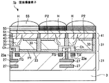
図2は、第1実施形態の固体撮像素子の構成を示す要部断面図であり、図1における画素領域5の3画素分の断面図である。この図1に示す固体撮像素子1aは、支持基板3上に、配線層21、半導体層31、光電変換膜41、保護膜51、カラーフィルタ層53、およびオンチップレンズ55をこの順に積層してなる。以下、下層側から順に構成を説明する。
≪2. Configuration of Solid-State Image Sensor of First Embodiment >>
FIG. 2 is a cross-sectional view of the main part showing the configuration of the solid-state imaging device of the first embodiment, and is a cross-sectional view of three pixels in the
[支持基板3]
支持基板3は、固体撮像素子の支持基板であり、ガラス基板、半導体基板、プラスチック基板など、適宜の材質のものが用いられる。
[Support substrate 3]
The
[配線層21]
配線層21は、例えば多層配線構造で構成されている。この配線層21は、半導体層31側の界面にゲート絶縁膜23を介して設けられた転送ゲートTGを有している。転送ゲートTGは、画素毎に設けられており、層間絶縁膜25で覆われている。配線層21は、この層間絶縁膜25によって絶縁性が確保された配線27を多層にわたって有している。また、層間絶縁膜25およびゲート絶縁膜23の一部には、半導体層31に達する接続孔25aが設けられ、この接続孔25aを介して配線27と半導体層31とが接続されている。
[Wiring layer 21]
The
[半導体層31]
半導体層31は、単結晶構造を有する薄膜状の層であり、例えば単結晶シリコンからなる半導体基板を薄膜化したものである。この半導体層31は、深さ方向に渡って設けられた素子分離33によって、複数の電荷蓄積部35に分離されている。各電荷蓄積部35は、例えばn+型不純物層またはp+型不純物層からなり、画素毎に対応して配置されている。一例として、電荷蓄積部35はn+型不純物層からなることとして以下の説明を行う。この場合、素子分離33は、p+型不純物層からなるか、または溝型素子分離(shallow trench isolation:STI)であっても良い。
[Semiconductor layer 31]
The
また半導体層31には、配線層21との界面側の一部に、p型不純物層からなるチャネル領域Chによって電荷蓄積部35に対して仕切られたn型不純物層からなるフローティングディフュージョンFDが設けられている。フローティングディフュージョンFDは、複数の電荷蓄積部35で1つのフローティングディフュージョンFDを共有する状態で設けられており、ここでは隣接する2画素の電荷蓄積部35で1つのフローティングディフュージョンFDを共有した状態を図示している。これにより、上述した素子分離33の一部は、チャネル領域Chに当接して設けられていることになる。
In addition, the
またフローティングディフュージョンFDに対して、配線層21に設けられた配線27の一部が接続された状態となっている。さらに、配線層21に設けられた転送ゲートTGは、フローティングディフュージョンFDと電荷蓄積部35との間のチャネル領域Ch上に対応して配置されている。
A part of the
またさらに半導体層31における配線層21との界面側には、電荷蓄積部35を覆う状態で第1ピニング層P1が設けられえている。この第1ピニング層P1は、電荷蓄積部35とは逆導電型(ここではp型)の不純物層からなり、薄い膜厚で構成される。
Furthermore, on the interface side of the
一方、半導体層31における光電変換膜41との界面側には、本第1実施形態に特徴的な第2ピニング層P2が設けられている。この第2ピニング層P2は、電荷蓄積部35とは逆導電型の不純物層からなり、ここでは例えばホウ素濃度1019個/cm3程度のp+不純物層からなる、このような第2ピニング層P2は、極薄い膜厚で構成されていることとする。
On the other hand, on the interface side of the
特に第2ピニング層P2は、一部を開口して電荷蓄積部35を覆う形状で設けられているところが特徴的であり、この開口Hにおいて半導体層31で構成された電荷蓄積部35が光電変換膜31と直接接している。第2ピニング層P2の開口Hは、例えば素子を支持基板3側から平面視的に見た場合に、フローティングディフュージョンFDと重ならない位置に配置されることとする。
In particular, the second pinning layer P2 is characterized in that a part of the second pinning layer P2 is opened and covers the
以上により、半導体層31における配線層21との界面および光電変換膜41との界面は、光電変換膜41側の開口H、フローティングディフュージョンFD、及びチャネル領域Chを除いて、p+不純物層からなる第1ピニング層P1、第2ピニング層P2、または素子分離33で覆われた状態となっている。
As described above, the interface of the
尚ここでの図示は省略したが、以上の半導体層31と配線層21との界面には、不純物層、ゲート絶縁膜、および転送ゲートと同一層からなる電極を用いたトランジスタTrや容量素子が設けられている。また、配線層21にはこれらの素子を接続する配線が設けられていて、上述した画素回路や周辺回路を構成している。特に本実施形態の固体撮像素子1aには、グローバルシャッタ回路が好適に用いられる。ここで用いられるグローバルシャッタ回路の構成が限定されることはなく、様々な構成のグローバルシャッタ回路を適用することが可能である。
Although illustration is omitted here, at the interface between the
[光電変換膜41]
光電変換膜41は、半導体層31上に成膜された層である。この光電変換膜41は、深さ方向に渡って設けられた素子分離43によって、複数の光電変換部45に分離されている。各光電変換部45は、画素毎に対応して配置されており、1つの光電変換部45が、1つの電荷蓄積部35における第2ピニング層P2の開口Hと1:1で接合していることが重要である。尚、素子分離43は、光電変換部45と逆導電型の不純物層からなるか、または溝型素子分離(shallow trench isolation:STI)であっても良い。
[Photoelectric conversion film 41]
The
また光電変換膜41は、半導体層31よりも可視光線の光吸収係数が高い材料で構成されていることが重要であり、吸収係数が高いほど好ましい。また光電変換膜41は、半導体層31に対して格子整合させた状態で設けられていることが好ましい。これにより、光電変換効率に優れた結晶性の高い光電変換膜41とすることができ、また光電変換膜41と半導体層31における電荷蓄積部35との間の界面準位が低く抑えられる。このように、半導体層31に対して格子整合させた光電変換膜41としては、半導体層31上にエピタキシャル成長させた層が好ましく用いられる。
Moreover, it is important that the
以上のような光電変換膜41は、例えば(1)化合物半導体材料、(2)シリサイド系材料、および(3)有機材料の中から適宜選択して用いられる。一例として、半導体層31が単結晶シリコンからなる場合、光電変換膜41を構成する(1)〜(3)の材料として、次の各材料が例示される。
The
(1)化合物半導体材料としては、特にカルコパイライト構造の化合物半導体材料が用いられる。カルコパイライト構造の化合物半導体材料は、高い光吸収係数と、広い波長域に渡る高い感度が得られる材料であり、光電変換膜41として好ましく用いられる。このようなカルコパイライト構造の半導体材料は、Cu、Al、Ga、In、Zn、S、Seなど、IV族元素の周囲の元素を用いて構成され、CuInSe系混晶、CuGaInS系混晶、CuAlGaInS系混晶、CuAlGaInSSe系混晶、およびCuAlGaInZnSSe系混晶等が例示される。これらの化合物半導体材料からなる光電変換膜41は、単結晶のほか、多結晶、非晶質の何れの結晶構造であっても良い。
(1) As the compound semiconductor material, a compound semiconductor material having a chalcopyrite structure is used. A compound semiconductor material having a chalcopyrite structure is a material that has a high light absorption coefficient and a high sensitivity over a wide wavelength range, and is preferably used as the
以上の化合物半導体材料のうち、光吸収係数の観点からは、CuInSe2が好適に用いられる。CuInSe2は、光吸収係数が他の材料よりも高く、特に、単結晶シリコンと比較して約2桁高い光吸収係数を有する。このため、CuInSe2からなる光電変換膜41であれば、可視光線を遮光する機能を有する光電変換膜41として好適に機能する。
Of the above compound semiconductor materials, CuInSe 2 is preferably used from the viewpoint of the light absorption coefficient. CuInSe 2 has a higher light absorption coefficient than other materials, and in particular has a light absorption coefficient that is about two orders of magnitude higher than that of single crystal silicon. For this reason, the
また以上の化合物半導体材料のうち、半導体層31に対する格子整合の観点からは、半導体層31が単結晶シリコンからなる場合に以下の組成が好ましく用いられる。
Cu(Ga0.52In0.48)S2
Cu(Al0.24Ga0.23In0.53)S2
Cu(Al0.36Ga0.64)(S1.28Se0.72)
Among the above compound semiconductor materials, from the viewpoint of lattice matching with respect to the
Cu (Ga 0.52 In 0.48 ) S 2
Cu (Al 0.24 Ga 0.23 In 0.53 ) S 2
Cu (Al 0.36 Ga 0.64 ) (S 1.28 Se 0.72 )
(2)シリサイド系材料としては、CoSi,CrSi,HfSi,IrSi,MoSi,NiSi,PdSi,ReSi,TaSi,TiSi,WSi,ZrSi,β−鉄シリサイド材料(β−FeSi2)、バリウムシリサイド系材料(BaSi2,BaSrSi)が例示される。 (2) As silicide materials, CoSi, CrSi, HfSi, IrSi, MoSi, NiSi, PdSi, ReSi, TaSi, TiSi, WSi, ZrSi, β-iron silicide material (β-FeSi 2 ), barium silicide material ( BaSi 2 , BaSrSi) is exemplified.
以上のシリサイド系材料のうち、光吸収係数の観点からは、β−鉄シリサイド材料(β−FeSi2)、バリウムシリサイド系材料(BaSi2,BaSrSi)が好適に用いられる。これらの材料は、単結晶シリコンと比較して約2桁高い光吸収係数を有するため、可視光線を遮光する機能を有する光電変換膜41を構成する材料として好適である。
Of the above silicide materials, β-iron silicide materials (β-FeSi 2 ) and barium silicide materials (BaSi 2 , BaSrSi) are preferably used from the viewpoint of the light absorption coefficient. Since these materials have a light absorption coefficient that is approximately two orders of magnitude higher than that of single crystal silicon, they are suitable as materials for forming the
(3)有機材料としては、キナクドリン系、クマリン系の有機材料が好適に用いられる。これらの有機材料は、単結晶シリコンと比較して約2桁高い光吸収係数を有するため、可視光線を遮光する機能を有する光電変換膜41を構成する材料として好適である。
(3) As the organic material, quinacridin-based and coumarin-based organic materials are preferably used. Since these organic materials have a light absorption coefficient that is about two orders of magnitude higher than that of single crystal silicon, they are suitable as materials for forming the
また光電変換膜41は、各光電変換部45で発生した電荷が、第2ピニング層P2の開口Hを介して半導体層31で構成された電荷蓄積部35に容易に移動するように、半導体層31側に向かって深さ方向にバンドが傾斜するように形成することが好ましい。例えば電荷蓄積部35がn型不純物層からなる場合であれば、光電変換部45で発生させた電子が電荷蓄積部35に移動し易いように、電荷蓄積部35における深さ方向の不純物濃度や組成が調整されている。このような光電変換膜41は、上記の条件を備えていれば、p型,i型、n型の何れであっても良い。
In addition, the
具体的な一例として、光電変換膜41がカルコパイライト構造のCu(Ga0.52In0.48)S2を用いて構成されている場合を例示する。この場合、半導体層31で構成されるn型の電荷蓄積部35に対して、Cu(Ga0.52In0.48)S2を用いた光電変換膜41で構成される光電変換部45はp型になる。そこで、光電変換膜41(光電変換部45)は、Cu(Ga0.52In0.48)S2に対して、半導体層31に近い部分ほどn型不純物であるZnの濃度が高くなるように、深さ方向に濃度勾配を有してZnを含有する。光電変換膜41の膜厚が300nm程度であれば、n型不純物であるZnの濃度は、1014〜1016個/cm3程度である。これにより、p型の光電変換部45からn型の電荷蓄積部35に向かって電子が移動し易いようにバンドが傾斜した構成となる。
As a specific example, a case where the
以上のように、カルコパイライト構造の材料を用いて光電変換膜41を構成する場合であれば、光電変換膜41におけるIV族元素の周囲の元素を、深さ方向に濃度勾配をつけて含有させることにより、深さ方向にバンドを傾斜させることができる。
As described above, in the case where the
[保護膜51]
保護膜51は、パッシベーション性を有する材料膜の他、光電変換膜41が結晶構造である場合に、その欠陥準位を補償するための固定電荷を有する材料膜が用いられる。
[Protective film 51]
As the
パッシベーション性を有する材料膜としては、通常の酸化シリコン膜、窒化シリコン膜、または酸窒化シリコン膜などが用いられる。 As the material film having passivation properties, a normal silicon oxide film, silicon nitride film, silicon oxynitride film, or the like is used.
一方、固定電荷を有する材料膜としては、例えば光電変換膜41がn型であれば、負の固定電荷を有する材料膜が成膜され、光電変換膜41がp型であれば、正の固定電荷を有する材料膜が用いられる。
On the other hand, as the material film having a fixed charge, for example, if the
一例として、負の固定電荷を有する材料膜としては、金属酸化膜やシリコン系材膜が用いられる。金属酸化膜であれば、その材料自体が負の固定電荷を有する材料であることが好ましく、例えば遷移金属酸化膜が用いられる。具体的には、酸化ハフニウム(HfO2)、酸化ジルコニウム(ZrO2)、酸化アルミニウム(Al2O3)、酸化チタン(TiO2)、または酸化タンタル(Ta2O5)が好ましく用いられる。シリコン系材料膜であれば、その材料自体が負の固定電荷を有する材料であることが好ましく、ホウ素や燐などの不純物を含有する酸化シリコン膜が好ましく用いられる。具体的には、ホウ素を含有する酸化シリコン(BSG)、燐を含有する酸化シリコン(PSG)、ホウ素とリンを含有する酸化シリコンBPSGである。 As an example, a metal oxide film or a silicon-based material film is used as the material film having a negative fixed charge. In the case of a metal oxide film, the material itself is preferably a material having a negative fixed charge. For example, a transition metal oxide film is used. Specifically, hafnium oxide (HfO 2 ), zirconium oxide (ZrO 2 ), aluminum oxide (Al 2 O 3 ), titanium oxide (TiO 2 ), or tantalum oxide (Ta 2 O 5 ) is preferably used. In the case of a silicon-based material film, the material itself is preferably a material having a negative fixed charge, and a silicon oxide film containing impurities such as boron and phosphorus is preferably used. Specifically, silicon oxide (BSG) containing boron, silicon oxide (PSG) containing phosphorus, and silicon oxide BPSG containing boron and phosphorus.
以上のような負の固定電荷を有する材料膜は、有機金属や有機シランガスを用いた成膜を行うことにより、炭素を含有する膜として形成することが好ましく、これによってさらに膜中における負の固定電荷を増加させることができる(特開2010−67736参照)。 The material film having a negative fixed charge as described above is preferably formed as a film containing carbon by performing film formation using an organic metal or an organic silane gas, thereby further negatively fixing in the film. The charge can be increased (see JP 2010-67736 A).
以上の他、負の固定電荷を有する材料膜としては、例えば透明電極材料膜が用いられる。光電変換膜41がn型であれば、透明電極材料膜からなる保護膜51に負の電圧を印加することより、当該保護膜51を負の固定電荷を有する膜として用いることが可能になる。
In addition to the above, as the material film having a negative fixed charge, for example, a transparent electrode material film is used. If the
また正の固定電荷を有する材料膜としては、例えば透明電極材料膜が用いられる。光電変換膜41がp型であれば、透明電極材料膜からなる保護膜51に正の電圧を印加することより、当該保護膜51を正の固定電荷を有する膜として用いることが可能になる。
As the material film having a positive fixed charge, for example, a transparent electrode material film is used. If the
尚、上述した保護膜51は、単層構造であっても積層構造であっても良い。積層構造である場合には、固定電荷を有する材料膜の上部にパッシベーション性を有する材料膜を積層させた積層構造として形成しても良い。
The
[カラーフィルタ層53]
カラーフィルタ層53は、各光電変換部45に対応して1:1で設けられた各色のカラーフィルタで構成されている。各色のカラーフィルタの配列が限定されることはない。
[Color filter layer 53]
The
[オンチップレンズ55]
オンチップレンズ55は、各光電変換部45およびカラーフィルタ層53を構成する各色のカラーフィルタに対応して1:1で設けられ、各光電変換部45に入射光が集光されるように構成されている。
[On-chip lens 55]
The on-
以上のように構成された固体撮像素子1aでは、電荷蓄積部35を構成する半導体層31上に光電変換膜41を設けている。このため、光電変換膜41として光吸収性の良好な膜を用いることにより、光電変換膜41側から入射した光の半導体層31側への透過が抑制される。これにより、半導体層31からなる電荷蓄積部35への光照射によるノイズの発生を防止できる。
In the solid-
しかも、電荷蓄積部35における光電変換膜41との界面に、電荷蓄積部35とは逆導電型の第2ピニング層P2を設けたことで、界面を固定電位、例えば0Vや負電位にすることができ、いわゆるバーチャルゲートとしてのピニング効果が得られる。これにより、半導体層31からなる電荷蓄積部35において、光電変換膜41側の界面の欠陥準位が補償される。また図2中に矢印で示したように、光電変換膜41で生成された信号電荷は、第2ピニング層P2に設けた開口Hを介して接合された電荷蓄積部35に移動して蓄積される。したがって、光電変換膜41における光電変換部45から電荷蓄積部35への電荷の移動を妨げることなく、界面の欠陥準位に起因する暗電流の発生や、これによる白傷の発生を防止できる。
In addition, by providing the second pinning layer P2 having a conductivity type opposite to that of the
以上の結果、光電変換部45と配線層21とを積層させたことで受光感度の向上および画素の高密度化が達成される構成の固体撮像素子1aにおいて、ノイズの発生を防止して画像品質の向上を図ることが可能になる。
As a result, in the solid-
特に、グローバルシャッタ回路を備えてグローバルシャッタ方式での撮像を行う固体撮像素子1aにおいては、各光電変換部45が設けられた全画素において同時に露光が実施されて、各電荷蓄積部35に一旦信号電荷が蓄積される。このため、電荷蓄積部35に光が入射した場合のノイズの発生が顕著になるが、本第1実施形態の適用によってこのようなノイズの発生を確実に防止可能である。したがって、本第1実施形態の構成は、グローバルシャッタ方式での撮像を行う固体撮像素子1aにおいて顕著な画像品質向上の効果を得ることが可能である。
In particular, in the solid-
≪3.第1実施形態に対応させた固体撮像素子の製造方法の第1例≫
図3および図4は、第1実施形態に対応させた固体撮像素子の製造方法の第1例を説明するための断面工程図である。以下、これらの図に基づいて第1実施形態の固体撮像素子の製造方法の第1例を説明する。
≪3. First Example of Manufacturing Method of Solid-State Imaging Device Corresponding to First Embodiment >>
3 and 4 are cross-sectional process diagrams for describing a first example of a method for manufacturing a solid-state imaging device corresponding to the first embodiment. Hereinafter, a first example of the manufacturing method of the solid-state imaging device of the first embodiment will be described based on these drawings.
[図3(A)]
先ず、図3(A)に示すように、半導体基板31aとして、例えばn型の単結晶シリコン基板を用意する。
[FIG. 3 (A)]
First, as shown in FIG. 3A, for example, an n-type single crystal silicon substrate is prepared as the
この半導体基板31aの表面層に、先に説明したp+型不純物層からなる素子分離33、第1ピニング層P1、および第2ピニング層P2を形成し、さらにp型不純物層からなるチャネル領域Chを形成する。またn+型不純物層からなるフローティングディフュージョンFDおよび電荷蓄積部35を形成する。
On the surface layer of the
これらの各p+型不純物層、p型不純物層、およびn+型不純物層の形成は、半導体基板31aの表面側からの不純物導入によって行われ、例えばマスク上からのイオン注入と、その後の活性化熱処理とによって行う。p+型不純物層およびp型不純物層であれば、ホウ素(B)のようなp型不純物のイオン注入を行う。一方、n+型不純物層であれば、ヒ素(As)のようなn型の不純物のイオン注入を行う。イオン注入は、それぞれの不純物層の深さに合わせて注入エネルギーを適宜に設定して行う。
Each of these p + type impurity layer, p type impurity layer, and n + type impurity layer is formed by introducing impurities from the surface side of the
例えば、一部に開口Hを有する第2ピニング層P2の形成においては、開口Hに対応する部分を覆うマスクを半導体基板31aの表面上に形成し、このマスク上からのイオン注入を行う。また第1ピニング層P1よりも深い位置に形成される第2ピニング層P2は、第1ピニング層P1の形成よりも注入エネルギーを高く設定したイオン注入を適用する。これにより、例えばホウ素濃度1019個/cm3程度のp+不純物層からなる第2ピニング層P2を形成する。
For example, in the formation of the second pinning layer P2 having a part of the opening H, a mask covering a part corresponding to the opening H is formed on the surface of the
次に、半導体基板31aにおいて電荷蓄積部35が形成された表面上に、酸化シリコン膜や窒化シリコン膜を用いたゲート絶縁膜23を成膜し、さらにこの上部にポリシリコンからなる転送ゲートTGを形成する。
Next, a
以上までの工程は、特に工程手順が限定されることはなく、適宜の手順で行うことができる。例えば、ゲート絶縁膜23上に転送ゲートTGを形成した後、転送ゲートTGをマスクに用いてフローティングディフュージョンFDや第1ピニング層P1を形成するためのイオン注入を行っても良い。また、素子分離33は、不純物層からなるものに限定されず、溝型素子分離として形成しても良い。
The process steps up to the above are not particularly limited, and can be performed according to an appropriate procedure. For example, after forming the transfer gate TG on the
[図3(B)]
次に図3(B)に示すように、半導体基板31a上に、転送ゲートTGを覆う状態で層間絶縁膜25を形成し、さらにフローティングディフュージョンFDに達する接続孔25aを層間絶縁膜25およびゲート絶縁膜23に形成する。
[Fig. 3 (B)]
Next, as shown in FIG. 3B, the
次に接続孔25aを介してフローティングディフュージョンFDに接続された配線27の形成、層間絶縁膜25の形成、配線27の形成、および層間絶縁膜25の形成を繰り返し行う。配線27は、アルミニウム、タングステン、またはモリブデン等、導電性の良好な金属材料を用いて形成されることとする。また最上層の層間絶縁膜25は、埋め込み特性の良好な膜で構成し、表面平坦に形成されることとする。
Next, the formation of the
これにより、ゲート絶縁膜23、転送ゲートTG、および層間絶縁膜25で絶縁された多層構造の配線27を有する配線層21を形成する。
As a result, the
また以上の工程により、半導体基板31aおよび配線層21には、画素回路や周辺回路を構成するトランジスタTr、容量素子、および配線を形成する。
Through the above steps, the transistor Tr, the capacitor element, and the wiring that form the pixel circuit and the peripheral circuit are formed in the
尚、配線層21の形成工程は、通常の半導体プロセスにしたがって行えば良く、工程手順が限定されることはない。例えば、配線27の形成にはいわゆるダマシン工程を適用しても良く、この場合、銅(Cu)等のエッチング加工に不向きな金属材料を用いて配線27を形成することができる。
In addition, the formation process of the
[図3(C)]
その後、図3(C)に示すように、配線層21における層間絶縁膜25の上部に支持基板3を張り合わせる。支持基板3の張り合わせは、ここでの図示を省略した接着剤を介して行うか、また接着剤を使用しない直接接合で行なってもよい。
[Fig. 3 (C)]
Thereafter, as shown in FIG. 3C, the
[図4(A)]
次に、図4(A)に示すように、半導体基板31aを裏面側から薄膜化して半導体層31とする。ここでは、第2ピニング層P2と共に電荷蓄積部35が露出するまで、支持基板3と反対側の面から半導体基板31aを薄膜化して半導体層31とする。この際、第2ピニング層P2をエッチングストッパとした研磨やエッチングを行うことにより、半導体基板31aを薄膜化する。
[FIG. 4 (A)]
Next, as illustrated in FIG. 4A, the
[図4(B)]
その後、図4(B)に示すように、半導体層31の露出面上に、光電変換膜41を成膜する。光電変換膜41の成膜は、光電変換部41を構成する上述した各材料によって適宜の成膜方法を適用して行われる。
[Fig. 4 (B)]
Thereafter, as illustrated in FIG. 4B, a
例えば、カルコパイライト構造の化合物半導体からなる光電変換膜41を、半導体層31に対して格子整合させて形成する場合ではれば、半導体層31に対して光電変換膜41をエピタキシャル成長させる。これにより、単結晶シリコンからなる半導体層31に対して格子整合した状態で、予め結晶構造を有する光電変換膜41が成膜される。このような光電変換膜41のエピタキシャル成長による成膜は、光電変換膜41を構成する各元素を含有する成膜ガスを用いた化学的気相成長(Chemical Vapor deposition:CVD)法や、分子線エピタキシャル成長(Molecular Beam Epitaxy:MBE)法によって行われる。
For example, when the
例えば、カルコパイライト構造のCu(Ga0.52In0.48)S2を用いた光電変化膜41を成膜する場合であれば、p型のCu(Ga0.52In0.48)S2に対してn型不純物であるZnを添加した成膜を行う。この際、Znの濃度が結晶成長と共に低下するように、Znを含有する成膜ガスの供給量を調整した成膜を行う。これにより、p型の光電変換膜41からn型の電荷蓄積部35に向かって電子が移動し易いようにバンドが傾斜した構成とする。
For example, when the
[図4C]
次に、図4Cに示すように、光電変換膜41に素子分離43を形成し、光電変換膜41を各画素毎に分離してなる光電変換部45を形成する。ここでは、例えばリソグラフィー法によって光電変換膜41上にマスクパターンを形成し、このマスクパターン上からのイオン注入とその後の活性化熱処理とによって、第2体薄層41の深さ方向にわたる不純物層を形成してこれを素子分離43とする。この際、光電変換膜41がp型であればn型の不純物をイオン注入によって導入し、光電変換膜41がn型であればp型の不純物をイオン注入によって導入する。
[FIG. 4C]
Next, as illustrated in FIG. 4C, the
尚、素子分離43の形成は、溝内を絶縁膜で埋め込んでも良い。この場合、光電変換膜41の導電型によらずに溝型素子分離(shallow trench isolation:STI)が形成される。素子分離43を溝型素子分離として形成することにより、素子分離43の形成に不純物の活性化熱処理を行う必要がないため好ましい。
The
[図2]
以上の後、先の図2に示したように、光電変換部45を構成する光電変換膜41上に、保護膜51を成膜する。この保護膜51は、上述したように、パッシベーション性を有する材料膜の他、光電変換膜41表面の欠陥準位を補償するための固定電荷を有する材料膜が用いられる。
[Figure 2]
After the above, as shown in FIG. 2 above, the
次で、保護膜51上に、各光電変換部45に対応させて、各色フィルタをパターン形成してなるカラーフィルタ層53を形成し、さらにオンチップレンズ55を形成する。以上により、固体撮像素子1aが得られる。
Next, a
以上説明した第1例の製造方法により、図2を用いて説明したように、半導体層31からなる電荷蓄積部35において、光電変換膜41からなる光電変換部45との界面側の部分に、第2ピニング層P2を設けた第1実施形態の固体撮像素子を得ることができる。特に本第1例の手順によれば、図3(A)を用いて説明したように、半導体層31を構成する半導体基板31aに電荷蓄積部35等の不純物層を形成した後に、図3(B)を用いて説明したように半導体基板31a上に配線27を形成する工程を行う。このため、不純物層を形成するための高温での活性化熱処理の影響が配線27に及ぶことがなく、配線27の品質を維持することが可能である。また、光電変換膜41に形成する素子分離43を溝型素子分離として形成することにより、素子分離43の形成に不純物の活性化熱処理を行う必要がないため、配線27への熱処理の影響を抑えることができ、配線27の品質を維持することが可能である。
With the manufacturing method of the first example described above, as described with reference to FIG. 2, in the
≪4.第1実施形態に対応させた固体撮像素子の製造方法の第2例≫
図5および図6は、第1実施形態に対応させた固体撮像素子の製造方法の第2例を説明するための断面工程図である。本第2例が、先に説明した第1例と異なるところは、全体の工程中において第2ピニング層P2を形成するタイミングであって、他の手順は同様である。以下、図5,6に基づいて第1実施形態の固体撮像素子の製造方法の第2例を説明する。尚、第1例と重複する工程の詳細な説明は省略する。
<< 4. Second Example of Manufacturing Method of Solid-State Imaging Device Corresponding to First Embodiment >>
5 and 6 are cross-sectional process diagrams for explaining a second example of the method of manufacturing the solid-state imaging device corresponding to the first embodiment. The difference between the second example and the first example described above is the timing at which the second pinning layer P2 is formed during the entire process, and the other procedures are the same. Hereinafter, a second example of the method for manufacturing the solid-state imaging device according to the first embodiment will be described with reference to FIGS. Detailed description of the same steps as those in the first example will be omitted.
[図5(A)]
先ず、図5(A)に示すように、半導体基板31aとして、例えばn型の単結晶シリコン基板を用意する。
[FIG. 5 (A)]
First, as shown in FIG. 5A, for example, an n-type single crystal silicon substrate is prepared as the
この半導体基板31aの表面層に、第2ピニング層P2以外の不純物層を形成する。すなわち、p+型不純物層からなる素子分離33および第1ピニング層P1を形成し、さらにp型不純物層からなるチャネル領域Chを形成する。またn+型不純物層からなるフローティングディフュージョンFDおよび電荷蓄積部35を形成する。尚ここでは、チャネル領域Chで囲まれた半導体基板31aの表面層が電荷蓄積部35となる。
Impurity layers other than the second pinning layer P2 are formed on the surface layer of the
これらの各p+型不純物層、p型不純物層、およびn+型不純物層の形成は、マスク上からのイオン注入と、その後の活性化熱処理とによって行い、特にイオン注入は、それぞれの不純物層の深さに合わせて注入エネルギーを適宜に設定して行う。 Each of these p + type impurity layer, p type impurity layer, and n + type impurity layer is formed by ion implantation from above the mask and subsequent activation heat treatment. In particular, ion implantation is performed at the depth of each impurity layer. In accordance with this, the implantation energy is set appropriately.
次に、半導体基板31aにおいて電荷蓄積部35が形成された表面上に、酸化シリコン膜や窒化シリコン膜を用いたゲート絶縁膜23を成膜し、さらにこの上部にポリシリコンからなる転送ゲートTGを形成する。
Next, a
[図5(B)]
次に図5(B)に示すように、半導体基板31a上に、層間絶縁膜25、フローティングディフュージョンFDに達する接続孔25a、および接続孔25aを介してフローティングディフュージョンFDに接続された配線27を有する配線層21を形成する。これにより、半導体基板31aおよび配線層21には、画素回路や周辺回路を構成するトランジスタTr、容量素子、および配線を形成する。
[Fig. 5 (B)]
Next, as shown in FIG. 5B, an
[図5(C)]
その後、図5(C)に示すように、配線層21における層間絶縁膜25の上部に支持基板3を張り合わせる。支持基板3の張り合わせは、ここでの図示を省略した接着剤を介して行う。
[FIG. 5C]
Thereafter, as shown in FIG. 5C, the
[図6(A)]
次に、図6(A)に示すように、電荷蓄積部35を残し記半導体基板31aを裏面側から薄膜化して半導体層31とする。ここでは、電荷蓄積部35として必要な膜厚となるように半導体基板31aを薄膜化する。
[FIG. 6 (A)]
Next, as shown in FIG. 6A, the
[図6(B)]
その後、図6(B)に示すように、単結晶シリコンからなる半導体層31の露出表面層、すなわちn+型不純物層からなる電荷蓄積部35の露出表面層に、p+型不純物層からなる第2ピニング層P2を形成する。第2ピニング層P2の形成は、半導体層31の露出表面側からの不純物導入によって行われ、例えば開口Hに対応する部分を覆うマスク上からのイオン注入と、その後の活性化熱処理とによって行う。このイオン注入は、注入エネルギーを低く保つことにより、半導体層31の極表面層のみに第2ピニング層P2が形成されるように行う。
[Fig. 6 (B)]
Thereafter, as shown in FIG. 6B, the second surface made of the p + type impurity layer is formed on the exposed surface layer of the
尚、第2ピニング層P2を形成するための不純物の活性加熱処理は、レーザーアニールによって行うことができる。 The active heat treatment of impurities for forming the second pinning layer P2 can be performed by laser annealing.
[図6(C)]
以上の後、図6(C)に示すように、半導体層31の露出面上に光電変換膜41を成膜する。例えば、カルコパイライト構造の化合物半導体からなる光電変換膜41を、半導体層31に対して格子整合させて形成する場合であれば、半導体層31に対して光電変換膜41をエピタキシャル成長させる。
[Fig. 6 (C)]
After the above, a
ここでは上述した第1例と同様に、例えば、カルコパイライト構造のCu(Ga0.52In0.48)S2を用いた光電変化膜41を成膜する場合であれば、p型のCu(Ga0.52In0.48)S2に対してn型不純物であるZnを添加した成膜を行う。この際、Znの濃度が結晶成長と共に低下するように、Znを含有する成膜ガスの供給量を調整した成膜を行う。これにより、p型の光電変換膜41からn型の電荷蓄積部35に向かって電子が移動し易いようにバンドが傾斜した構成とする。
Here, similarly to the first example described above, for example, in the case of forming the
その後、光電変換膜41に素子分離43を形成し、光電変換膜41を各画素毎に分離してなる光電変換部45を形成する。尚、素子分離43の形成は、溝内を絶縁膜で埋め込んでも良い。この場合、光電変換膜41の導電型によらずに溝型素子分離(shallow trench isolation:STI)が形成される。素子分離43を溝型素子分離として形成することにより、素子分離43の形成に不純物の活性化熱処理を行う必要がないため好ましい。
Thereafter, an
[図2]
以上の後、先の図2に示したように、光電変換部45を構成する光電変換膜41上に、保護膜51を成膜する。この保護膜51は、上述したように、パッシベーション性を有する材料膜の他、光電変換膜41表面の欠陥準位を補償するための固定電荷を有する材料膜が用いられる。
[Figure 2]
After the above, as shown in FIG. 2 above, the
次で、保護膜51上に、各光電変換部45に対応させて、各色フィルタをパターン形成してなるカラーフィルタ層53を形成し、さらにオンチップレンズ55を形成する。以上により、固体撮像素子1aが得られる。
Next, a
以上説明した第2例の製造方法により、図2を用いて説明したように、半導体層31からなる電荷蓄積部35において、光電変換膜41からなる光電変換部45との界面側の部分に、第2ピニング層P2を設けた第1実施形態の固体撮像素子を得ることができる。特に本第2例の手順によれば、図6(B)を用いて説明したように、半導体基板31aを薄膜化した半導体層31の露出表面層への不純物導入によって第2ピニング層P2を形成する。このため、第2ピニング層P2を形成するための不純物の深さプロファイルの広がりを抑えることができ、半導体層31の露出表面層に極薄い第2ピニング層P2を形成することができる。したがって、青感度の向上と飽和電荷量の向上が見込まれる。
With the manufacturing method of the second example described above, as described with reference to FIG. 2, in the
また、第2ピニング層P2を形成するための不純物の活性加熱処理をレーザーアニールによって行うことができるため、配線層21よりも後に行われる第2ピニング層P2の高温での活性化を最表面だけで行うことができる。これにより、不純物層を形成するための高温での活性化熱処理の影響が配線27に及ぶことが抑えられ、配線27の品質を維持することが可能である。また、光電変換膜41に形成する素子分離43を溝型素子分離として形成することにより、素子分離43の形成に不純物の活性化熱処理を行う必要がないため、配線27への熱処理の影響を抑えることができ、配線27の品質を維持することが可能である。
Further, since the active heat treatment of impurities for forming the second pinning layer P2 can be performed by laser annealing, the second pinning layer P2 that is performed after the
≪5.第2実施形態の固体撮像素子の構成≫(ピニング開口と転送ゲートとが重なる例)
図7は、第2実施形態の固体撮像素子の構成を示す要部断面図であり、図1における画素領域5の3画素分の断面図である。図7に示す第2実施形態の固体撮像素子1bが、図2を用いて説明した第1実施形態の固体撮像素子と異なるところは、第2ピニング層P2に設けた開口Hの平面視的な位置にあり、他の構成は第1実施形態と同様であることとする。
≪5. Configuration of Solid-State Image Sensor of Second Embodiment >> (Example in which pinning aperture and transfer gate overlap)
FIG. 7 is a cross-sectional view of the main part showing the configuration of the solid-state imaging device of the second embodiment, and is a cross-sectional view of three pixels in the
すなわち、第2ピニング層P2の開口Hは、配線層27に設けられた転送ゲートTGと平面視的に重なる位置に配置されている。図8(A)、図8(B)には、第2ピニング層P2側からの平面図を示す。これらの図に示すように、第2ピニング層P2の開口Hと転送ゲートTGとの重なり方が限定されることはなく、一部が重なっていれば良い。
That is, the opening H of the second pinning layer P2 is disposed at a position overlapping the transfer gate TG provided in the
以上のような第2実施形態の固体撮像素子1bでは、第2ピニング層P2の開口Hと転送ゲートTGとが重ねて配置されたことにより、開口Hから転送ゲートTGまでの距離が最短化される。これにより、図7中に矢印で示したように、光電変換膜41で生成された信号電荷は、転送ゲートTGの駆動によって直ちに第2ピニング層P2に設けた開口HからフローティングディフュージョンFDに読み出される。したがって、第1実施形態で説明したように、受光感度の向上および画素の高密度化が達成される構成においてノイズの発生を防止して画像品質の向上を図る効果に加え、光電変換部45からの電荷の読み出しが容易で応答特性の向上を図る効果を得ることができる。
In the solid-
≪6.第3実施形態の固体撮像素子の構成≫(ピニング開口を画素中央に設けた例)
図9は、第3実施形態の固体撮像素子の構成を示す要部断面図であり、図1における画素領域5の3画素分の断面図である。図9に示す第3実施形態の固体撮像素子1cが、先に説明した第1実施形態および第2実施形態の固体撮像素子と異なるところは、第2ピニング層P2に設けた開口Hの平面視的な位置にあり、他の構成は第1実施形態および第2実施形態と同様であることとする。
≪6. Configuration of Solid-State Image Sensor of Third Embodiment >> (Example in which a pinning aperture is provided at the center of a pixel)
FIG. 9 is a cross-sectional view of the main part showing the configuration of the solid-state imaging device of the third embodiment, and is a cross-sectional view of three pixels in the
すなわち、第2ピニング層P2の開口Hは、平面視的に光電変換部45の中央に配置されている。ここでは、光電変換部45は、電荷蓄積部35とほぼ一致した状態で積層されていることとする。この場合、第2ピニング層P2の開口Hは、光電変換部45および電荷蓄積部35の中央であって、画素の中央に配置された状態となる。図10(A)、図10(B)には、第2ピニング層P2側からの平面図を示す。これらの図に示すように、第2ピニング層P2の開口Hの形状は、四角形であっても円形であっても他の形状であっても良く、加工が容易な形状であれば好ましい。また第2実施形態で説明したように、第2ピニング層P2の開口Hは、転送ゲートTGと重なっていても良い。
That is, the opening H of the second pinning layer P2 is disposed in the center of the
以上のような第3実施形態の固体撮像素子1cでは、平面視的に見て光電変換部45の中央に第2ピニング層P2の開口Hを配置した構成である。これにより、転送ゲートTGの駆動による電界の影響が、第2ピニング層P2を介して光電変換部45の全域に対して均一に及ぶようになり、ポテンシャル設計が容易になる。このため、光電変換部45の全域から電荷蓄積部35に対して効率的に信号電荷を読み出すことが可能になる。したがって、第1実施形態で説明したように、受光感度の向上および画素の高密度化が達成される構成においてノイズの発生を防止して画像品質の向上を図る効果に加え、光電変換部45からの電荷の読み出しを効率的に行う効果を得ることができる。
The solid-
≪7.電子機器の実施形態≫
上述の各実施形態で説明した本発明に係る固体撮像素子は、例えばデジタルカメラやビデオカメラ等のカメラシステムや、撮像機能を有する携帯電話、あるいは撮像機能を備えた他の機器、などの電子機器に適用することができる。
≪7. Embodiment of Electronic Device >>
The solid-state imaging device according to the present invention described in each of the above embodiments is an electronic device such as a camera system such as a digital camera or a video camera, a mobile phone having an imaging function, or another device having an imaging function. Can be applied to.
図11は、本発明に係る電子機器の一例として、固体撮像素子を用いたカメラの構成図を示す。本実施形態例に係るカメラは、静止画像又は動画撮影可能なビデオカメラを例としたものである。本実施形態例のカメラ91は、固体撮像素子1と、固体撮像素子1の受光センサ部に入射光を導く光学系93と、シャッタ装置94と、固体撮像素子1を駆動する駆動回路95と、固体撮像素子1の出力信号を処理する信号処理回路96とを有する。
FIG. 11 is a configuration diagram of a camera using a solid-state imaging device as an example of the electronic apparatus according to the invention. The camera according to the present embodiment is an example of a video camera capable of capturing still images or moving images. The
固体撮像素子1は、上述した各実施形態および各変形例で説明した構成の固体撮像素子(1a,1b,1c)が適用される。光学系(光学レンズ)93は、被写体からの像光(入射光)を固体撮像素子1の撮像面上に結像させる。これにより、固体撮像素子1内に、一定期間信号電荷が蓄積される。光学系93は、複数の光学レンズから構成された光学レンズ系としても良い。シャッタ装置94は、固体撮像素子1への光照射期間及び遮光期間を制御する。駆動回路95は、固体撮像素子1の転送動作及びシャッタ装置94のシャッタ動作を制御する駆動信号を供給する。駆動回路95から供給される駆動信号(タイミング信号)により、固体撮像素子1の信号転送を行う。信号処理回路96は、各種の信号処理を行う。信号処理が行われた映像信号は、メモリなどの記憶媒体に記憶され、或いは、モニタに出力される。
As the solid-
以上説明した本実施形態に係る電子機器によれば、高密度でありながらも受光感度および画像品質の向上を図ることが可能な各実施形態の固体撮像素子1を用いたことにより、小型化および撮像画像の高品質化を達成することが可能になる。
According to the electronic apparatus according to the present embodiment described above, the use of the solid-
1,1a,1b,1c…固体撮像素子、21…配線層、23…ゲート絶縁膜、31…半導体層、31a…半導体基板、35…電荷蓄積部、41…光電変換膜、45…光電変換部、91…電子機器、93…光学系、96…信号処理回路、FD…フローティングディフュージョン、H…開口、P1…第1ピニング層、P2…第2ピニング層、TG…転送ゲート
DESCRIPTION OF
Claims (13)
前記配線層上に設けられた半導体層からなる電荷蓄積部と、
前記半導体層上に設けられた光電変換膜とを備え、
前記電荷蓄積部における前記光電変換膜との界面には、当該電荷蓄積部とは逆導電型のピニング層が一部を開口して設けられた
固体撮像素子。 A wiring layer;
A charge storage portion made of a semiconductor layer provided on the wiring layer;
A photoelectric conversion film provided on the semiconductor layer,
A solid-state imaging device in which a pinning layer having a conductivity type opposite to that of the charge storage unit is provided at an interface of the charge storage unit with the photoelectric conversion film.
前記配線層における前記半導体層との界面側には、ゲート絶縁膜を介して前記電荷蓄積部と前記フローティングディフュージョンとの間に位置する転送ゲートが設けられている
請求項1記載の固体撮像素子。 On the interface side of the semiconductor layer with the wiring layer, a floating diffusion is provided,
The solid-state imaging device according to claim 1, wherein a transfer gate located between the charge storage portion and the floating diffusion is provided on an interface side of the wiring layer with the semiconductor layer via a gate insulating film.
請求項2記載の固体撮像素子。 The solid-state imaging device according to claim 2, wherein the opening and the transfer gate are arranged so as to overlap in plan view.
請求項2記載の固体撮像素子。 The solid-state imaging device according to claim 2, wherein the opening and the transfer gate are arranged without overlapping in plan view.
前記ピニング層に設けられた開口は、平面視的に前記各光電変換部の中央に配置されている
請求項1〜4の何れかに記載の固体撮像素子。 The photoelectric conversion film is element-isolated into each photoelectric conversion unit corresponding to the charge storage unit,
The solid-state imaging device according to claim 1, wherein the opening provided in the pinning layer is disposed in the center of each photoelectric conversion unit in plan view.
請求項1〜5の何れかに記載の固体撮像素子。 The solid-state imaging device according to claim 1, wherein the photoelectric conversion film is made of a material having a higher absorption coefficient of visible light than the semiconductor layer.
前記光電変換膜は、前記半導体層に対して格子整合させて設けられている
請求項1〜6の何れかに記載の固体撮像素子。 The semiconductor layer is made of single crystal silicon,
The solid-state imaging device according to claim 1, wherein the photoelectric conversion film is provided in lattice matching with the semiconductor layer.
請求項1〜7の何れかに記載の固体撮像素子。 The solid-state imaging device according to claim 1, wherein a pinning layer having a conductivity type opposite to that of the charge storage unit is provided on an interface side of the charge storage unit with the wiring layer.
前記半導体基板において前記電荷蓄積部が形成された表面上に配線層を形成する工程と、
前記電荷蓄積部が露出するまで前記半導体基板を裏面側から薄膜化して半導体層とする工程と、
前記半導体層の露出面上に光電変換膜を成膜する工程とを行うと共に、
前記光電変換膜を成膜する工程の前に、前記電荷蓄積部における前記光電変換膜との界面となる部分に、一部を開口した形状で当該電荷蓄積部とは逆導電型のピニング層を形成する工程を行う
固体撮像素子の製造方法。 Forming a charge storage portion on the surface side of the semiconductor substrate;
Forming a wiring layer on the surface of the semiconductor substrate on which the charge storage portion is formed;
Forming a semiconductor layer by thinning the semiconductor substrate from the back side until the charge storage portion is exposed;
And performing a step of forming a photoelectric conversion film on the exposed surface of the semiconductor layer,
Prior to the step of forming the photoelectric conversion film, a pinning layer having a conductivity type opposite to the charge storage unit is formed in a part of the charge storage unit that is an interface with the photoelectric conversion film. The manufacturing method of the solid-state image sensor which performs the process to form.
前記半導体基板を裏面側から薄膜化して半導体層とする工程では、前記ピニング層と共に当該ピニング層の開口から前記電荷蓄積部が露出するまで当該半導体基板を薄膜化する
請求項9記載の固体撮像素子の製造方法。 The step of forming the pinning layer is performed by introducing impurities from the surface side of the semiconductor substrate before the step of forming the wiring layer,
10. The solid-state imaging device according to claim 9, wherein in the step of thinning the semiconductor substrate from the back side to form a semiconductor layer, the semiconductor substrate is thinned together with the pinning layer until the charge storage portion is exposed from the opening of the pinning layer. Manufacturing method.
請求項9記載の固体撮像素子の製造方法。 The solid-state imaging device according to claim 9, wherein the step of forming the pinning layer is performed by introducing an impurity into an exposed surface layer of the semiconductor layer after performing the step of thinning the semiconductor substrate to form a semiconductor layer. Manufacturing method.
前記光電変換膜を成膜する工程では、前記半導体層上に当該光電変換膜をエピタキシャル成長させる
請求項9〜11の何れかに記載の固体撮像素子の製造方法。 The semiconductor layer is made of single crystal silicon,
The method for manufacturing a solid-state imaging element according to claim 9, wherein in the step of forming the photoelectric conversion film, the photoelectric conversion film is epitaxially grown on the semiconductor layer.
前記固体撮像素子の画素領域に入射光を導く光学系と、
前記固体撮像素子の出力信号を処理する信号処理回路とを備え、
前記固体撮像素子は、
配線層と、
前記配線層上に設けられた半導体層からなる電荷蓄積部と、
前記半導体層上に設けられた光電変換膜とを備え、
前記電荷蓄積部における前記光電変換膜との界面には、当該電荷蓄積部とは逆導電型のピニング層が一部を開口して設けられた
電子機器。 A solid-state image sensor;
An optical system that guides incident light to a pixel region of the solid-state imaging device;
A signal processing circuit for processing an output signal of the solid-state imaging device,
The solid-state imaging device is
A wiring layer;
A charge storage portion made of a semiconductor layer provided on the wiring layer;
A photoelectric conversion film provided on the semiconductor layer,
An electronic device in which a pinning layer having a conductivity type opposite to that of the charge storage unit is provided at a part of the interface of the charge storage unit with the photoelectric conversion film.
Priority Applications (5)
| Application Number | Priority Date | Filing Date | Title |
|---|---|---|---|
| JP2011014110A JP2012156310A (en) | 2011-01-26 | 2011-01-26 | Solid-state imaging device, method of manufacturing solid state imaging device, and electronic apparatus |
| TW100147810A TW201234571A (en) | 2011-01-26 | 2011-12-21 | Solid-state imaging element, method for producing solid-state imaging element, and electronic device |
| US13/344,059 US8917342B2 (en) | 2011-01-26 | 2012-01-05 | Solid-state imaging element, method for producing solid-state imaging element, and electronic device |
| KR1020120002267A KR20120099336A (en) | 2011-01-26 | 2012-01-09 | Solid-state imaging element, method for producing solid-state imaging element, and electronic device |
| CN201210015219XA CN102623463A (en) | 2011-01-26 | 2012-01-17 | Solid-state imaging element, method for producing solid-state imaging element, and electronic device |
Applications Claiming Priority (1)
| Application Number | Priority Date | Filing Date | Title |
|---|---|---|---|
| JP2011014110A JP2012156310A (en) | 2011-01-26 | 2011-01-26 | Solid-state imaging device, method of manufacturing solid state imaging device, and electronic apparatus |
Publications (1)
| Publication Number | Publication Date |
|---|---|
| JP2012156310A true JP2012156310A (en) | 2012-08-16 |
Family
ID=46543913
Family Applications (1)
| Application Number | Title | Priority Date | Filing Date |
|---|---|---|---|
| JP2011014110A Pending JP2012156310A (en) | 2011-01-26 | 2011-01-26 | Solid-state imaging device, method of manufacturing solid state imaging device, and electronic apparatus |
Country Status (5)
| Country | Link |
|---|---|
| US (1) | US8917342B2 (en) |
| JP (1) | JP2012156310A (en) |
| KR (1) | KR20120099336A (en) |
| CN (1) | CN102623463A (en) |
| TW (1) | TW201234571A (en) |
Cited By (11)
| Publication number | Priority date | Publication date | Assignee | Title |
|---|---|---|---|---|
| JP2014116472A (en) * | 2012-12-10 | 2014-06-26 | Canon Inc | Solid-state image pickup device and method for manufacturing the same |
| JP2015037154A (en) * | 2013-08-15 | 2015-02-23 | ソニー株式会社 | Imaging device and imaging apparatus |
| WO2015079944A1 (en) * | 2013-11-29 | 2015-06-04 | ソニー株式会社 | Solid-state image capturing element, manufacturing method therefor, and electronic device |
| JP2016103541A (en) * | 2014-11-27 | 2016-06-02 | キヤノン株式会社 | Solid-state imaging device |
| WO2017122537A1 (en) * | 2016-01-13 | 2017-07-20 | ソニー株式会社 | Light receiving element, method for manufacturing light receiving element, image capturing element and electronic device |
| JP2017126738A (en) * | 2016-01-13 | 2017-07-20 | ソニー株式会社 | Light receiving device, method of manufacturing the same, imaging device, and electronic device |
| JP2018037672A (en) * | 2017-10-18 | 2018-03-08 | キヤノン株式会社 | Solid-state image pickup device and camera |
| JPWO2017057278A1 (en) * | 2015-09-30 | 2018-07-26 | 株式会社ニコン | Imaging device and imaging apparatus |
| JPWO2017057277A1 (en) * | 2015-09-30 | 2018-07-26 | 株式会社ニコン | Imaging device and imaging apparatus |
| JP2020096374A (en) * | 2014-04-11 | 2020-06-18 | 株式会社半導体エネルギー研究所 | Image sensor |
| WO2021240998A1 (en) * | 2020-05-26 | 2021-12-02 | ソニーセミコンダクタソリューションズ株式会社 | Solid-state imaging element |
Families Citing this family (15)
| Publication number | Priority date | Publication date | Assignee | Title |
|---|---|---|---|---|
| WO2013111637A1 (en) * | 2012-01-23 | 2013-08-01 | ソニー株式会社 | Solid-state image pickup apparatus, method for manufacturing solid-state image pickup apparatus, and electronic apparatus |
| KR101931658B1 (en) * | 2012-02-27 | 2018-12-21 | 삼성전자주식회사 | Unit pixel of image sensor and image sensor including the same |
| JP2014112580A (en) * | 2012-12-05 | 2014-06-19 | Sony Corp | Solid-state image sensor and driving method |
| KR101409240B1 (en) * | 2012-09-18 | 2014-06-18 | 셀로코주식회사 | SoC Processor Architecture for Sensor Network |
| JP2015053296A (en) * | 2013-01-28 | 2015-03-19 | ソニー株式会社 | Semiconductor element and semiconductor device provided with the same |
| US9967501B2 (en) | 2014-10-08 | 2018-05-08 | Panasonic Intellectual Property Management Co., Ltd. | Imaging device |
| KR102384890B1 (en) * | 2015-01-13 | 2022-04-11 | 삼성전자주식회사 | Image sensor and method of forming the same |
| WO2017057444A1 (en) * | 2015-09-30 | 2017-04-06 | 株式会社ニコン | Image-capturing element and image-capturing device |
| CN106601758B (en) * | 2015-10-16 | 2020-06-09 | 中芯国际集成电路制造(上海)有限公司 | Semiconductor device, manufacturing method thereof and electronic device |
| JP6782431B2 (en) | 2016-01-22 | 2020-11-11 | パナソニックIpマネジメント株式会社 | Imaging device |
| CN107026961B (en) | 2016-01-29 | 2021-02-12 | 松下知识产权经营株式会社 | Image pickup apparatus |
| US11437418B2 (en) * | 2016-02-29 | 2022-09-06 | Sony Corporation | Solid-state image pickup device |
| KR102563588B1 (en) | 2016-08-16 | 2023-08-03 | 삼성전자주식회사 | Image sensor and method of fabricating the same |
| EP3739630A4 (en) * | 2018-01-11 | 2021-03-03 | Sony Semiconductor Solutions Corporation | Solid-state imaging device and electronic device |
| US10770489B2 (en) | 2018-03-30 | 2020-09-08 | Vishay Intertechnology, Inc. | Optoelectronic device arranged as a multi-spectral light sensor having a photodiode array with aligned light blocking layers and N-well regions |
Citations (11)
| Publication number | Priority date | Publication date | Assignee | Title |
|---|---|---|---|---|
| JPH0661467A (en) * | 1992-08-10 | 1994-03-04 | Nippon Hoso Kyokai <Nhk> | Stacked solid-state image sensing element |
| JP2001102557A (en) * | 1999-09-27 | 2001-04-13 | Toshiba Corp | Solid-state image pickup device and manufacturing method therefor |
| JP2004512686A (en) * | 2000-10-19 | 2004-04-22 | クォンタム セミコンダクター リミテッド ライアビリティ カンパニー | Method of manufacturing heterojunction photodiode integrated with CMOS |
| JP2005268738A (en) * | 2004-02-17 | 2005-09-29 | Sony Corp | Solid-state imaging device and its manufacturing method, and semiconductor integrated circuit device and its manufacturing method |
| JP2006135252A (en) * | 2004-11-09 | 2006-05-25 | Renesas Technology Corp | Solid imaging element |
| WO2006103733A1 (en) * | 2005-03-28 | 2006-10-05 | Fujitsu Limited | Image pickup device |
| JP2008508702A (en) * | 2004-07-28 | 2008-03-21 | クォンタム セミコンダクター リミテッド ライアビリティ カンパニー | Optical device monolithically integrated with CMOS |
| JP2008147333A (en) * | 2006-12-08 | 2008-06-26 | Sony Corp | Solid-state imaging device, manufacturing method thereof and imaging apparatus |
| JP2008305994A (en) * | 2007-06-07 | 2008-12-18 | Panasonic Corp | Solid-state photographing apparatus and method of manufacturing the same |
| JP2011146635A (en) * | 2009-01-21 | 2011-07-28 | Sony Corp | Solid-state imaging device, method for producing the same, and image pickup apparatus |
| WO2011116268A1 (en) * | 2010-03-19 | 2011-09-22 | Invisage Technologies, Inc. | Image sensors employing sensitized semiconductor diodes |
Family Cites Families (8)
| Publication number | Priority date | Publication date | Assignee | Title |
|---|---|---|---|---|
| KR20020096336A (en) * | 2001-06-19 | 2002-12-31 | 삼성전자 주식회사 | Cmos type image sensor |
| JP2006066456A (en) * | 2004-08-24 | 2006-03-09 | Fuji Photo Film Co Ltd | Solid state image sensor |
| JP4992446B2 (en) | 2006-02-24 | 2012-08-08 | ソニー株式会社 | Solid-state imaging device, manufacturing method thereof, and camera |
| JP2008182142A (en) | 2007-01-26 | 2008-08-07 | Sony Corp | Solid-state image sensor, method of manufacturing the same, and imaging device |
| JP2008258474A (en) * | 2007-04-06 | 2008-10-23 | Sony Corp | Solid-state image pickup device and imaging apparatus |
| KR100870821B1 (en) * | 2007-06-29 | 2008-11-27 | 매그나칩 반도체 유한회사 | Backside illuminated image sensor |
| US7989859B2 (en) * | 2008-02-08 | 2011-08-02 | Omnivision Technologies, Inc. | Backside illuminated imaging sensor with silicide light reflecting layer |
| US8618458B2 (en) * | 2008-11-07 | 2013-12-31 | Omnivision Technologies, Inc. | Back-illuminated CMOS image sensors |
-
2011
- 2011-01-26 JP JP2011014110A patent/JP2012156310A/en active Pending
- 2011-12-21 TW TW100147810A patent/TW201234571A/en unknown
-
2012
- 2012-01-05 US US13/344,059 patent/US8917342B2/en not_active Expired - Fee Related
- 2012-01-09 KR KR1020120002267A patent/KR20120099336A/en not_active Application Discontinuation
- 2012-01-17 CN CN201210015219XA patent/CN102623463A/en active Pending
Patent Citations (11)
| Publication number | Priority date | Publication date | Assignee | Title |
|---|---|---|---|---|
| JPH0661467A (en) * | 1992-08-10 | 1994-03-04 | Nippon Hoso Kyokai <Nhk> | Stacked solid-state image sensing element |
| JP2001102557A (en) * | 1999-09-27 | 2001-04-13 | Toshiba Corp | Solid-state image pickup device and manufacturing method therefor |
| JP2004512686A (en) * | 2000-10-19 | 2004-04-22 | クォンタム セミコンダクター リミテッド ライアビリティ カンパニー | Method of manufacturing heterojunction photodiode integrated with CMOS |
| JP2005268738A (en) * | 2004-02-17 | 2005-09-29 | Sony Corp | Solid-state imaging device and its manufacturing method, and semiconductor integrated circuit device and its manufacturing method |
| JP2008508702A (en) * | 2004-07-28 | 2008-03-21 | クォンタム セミコンダクター リミテッド ライアビリティ カンパニー | Optical device monolithically integrated with CMOS |
| JP2006135252A (en) * | 2004-11-09 | 2006-05-25 | Renesas Technology Corp | Solid imaging element |
| WO2006103733A1 (en) * | 2005-03-28 | 2006-10-05 | Fujitsu Limited | Image pickup device |
| JP2008147333A (en) * | 2006-12-08 | 2008-06-26 | Sony Corp | Solid-state imaging device, manufacturing method thereof and imaging apparatus |
| JP2008305994A (en) * | 2007-06-07 | 2008-12-18 | Panasonic Corp | Solid-state photographing apparatus and method of manufacturing the same |
| JP2011146635A (en) * | 2009-01-21 | 2011-07-28 | Sony Corp | Solid-state imaging device, method for producing the same, and image pickup apparatus |
| WO2011116268A1 (en) * | 2010-03-19 | 2011-09-22 | Invisage Technologies, Inc. | Image sensors employing sensitized semiconductor diodes |
Cited By (16)
| Publication number | Priority date | Publication date | Assignee | Title |
|---|---|---|---|---|
| JP2014116472A (en) * | 2012-12-10 | 2014-06-26 | Canon Inc | Solid-state image pickup device and method for manufacturing the same |
| JP2015037154A (en) * | 2013-08-15 | 2015-02-23 | ソニー株式会社 | Imaging device and imaging apparatus |
| US10009564B2 (en) | 2013-11-29 | 2018-06-26 | Sony Semiconductor Solutions Corporation | Solid-state image capturing element, manufacturing method therefor, and electronic device |
| WO2015079944A1 (en) * | 2013-11-29 | 2015-06-04 | ソニー株式会社 | Solid-state image capturing element, manufacturing method therefor, and electronic device |
| US10536659B2 (en) | 2013-11-29 | 2020-01-14 | Sony Semiconductor Solutions Corporation | Solid-state image capturing element, manufacturing method therefor, and electronic device |
| JP2020096374A (en) * | 2014-04-11 | 2020-06-18 | 株式会社半導体エネルギー研究所 | Image sensor |
| JP2016103541A (en) * | 2014-11-27 | 2016-06-02 | キヤノン株式会社 | Solid-state imaging device |
| JPWO2017057278A1 (en) * | 2015-09-30 | 2018-07-26 | 株式会社ニコン | Imaging device and imaging apparatus |
| JPWO2017057277A1 (en) * | 2015-09-30 | 2018-07-26 | 株式会社ニコン | Imaging device and imaging apparatus |
| JP2021044572A (en) * | 2015-09-30 | 2021-03-18 | 株式会社ニコン | Imaging element and imaging apparatus |
| JP2021044571A (en) * | 2015-09-30 | 2021-03-18 | 株式会社ニコン | Imaging element |
| JP2017126738A (en) * | 2016-01-13 | 2017-07-20 | ソニー株式会社 | Light receiving device, method of manufacturing the same, imaging device, and electronic device |
| US10580821B2 (en) | 2016-01-13 | 2020-03-03 | Sony Corporation | Light-receiving element, manufacturing method of the same, imaging device, and electronic apparatus |
| WO2017122537A1 (en) * | 2016-01-13 | 2017-07-20 | ソニー株式会社 | Light receiving element, method for manufacturing light receiving element, image capturing element and electronic device |
| JP2018037672A (en) * | 2017-10-18 | 2018-03-08 | キヤノン株式会社 | Solid-state image pickup device and camera |
| WO2021240998A1 (en) * | 2020-05-26 | 2021-12-02 | ソニーセミコンダクタソリューションズ株式会社 | Solid-state imaging element |
Also Published As
| Publication number | Publication date |
|---|---|
| KR20120099336A (en) | 2012-09-10 |
| CN102623463A (en) | 2012-08-01 |
| US20120188397A1 (en) | 2012-07-26 |
| TW201234571A (en) | 2012-08-16 |
| US8917342B2 (en) | 2014-12-23 |
Similar Documents
| Publication | Publication Date | Title |
|---|---|---|
| JP2012156310A (en) | Solid-state imaging device, method of manufacturing solid state imaging device, and electronic apparatus | |
| US9269735B2 (en) | Method of manufacturing solid-state imaging device, solid-state imaging device, and electronic apparatus | |
| US10903257B2 (en) | Solid-state imaging device, driving method for solid-state imaging device, and electronic appliance | |
| US9419045B2 (en) | Solid-state imaging device and electronic instrument | |
| KR102145642B1 (en) | Solid state imaging apparatus and electronic device | |
| US8614112B2 (en) | Method of damage-free impurity doping for CMOS image sensors | |
| KR20190129831A (en) | Imaging element, electronic device | |
| JP2008300446A (en) | Solid image-capturing element, manufacturing method therefore, and image-capturing device | |
| JP2009088286A (en) | Solid-state imaging device, method of manufacturing the same, and camera | |
| WO2015198878A1 (en) | Solid-state imaging element, manufacturing method therefor, and electronic device | |
| CN103367375B (en) | Solid camera head and its manufacture method and electronic equipment | |
| KR20140099811A (en) | Camera module, solid-state imaging device, and method of manufacturing the same | |
| US9343496B2 (en) | Solid-state imaging device, production method thereof and camera | |
| JP2007115787A (en) | Solid-state imaging element | |
| US20220005851A1 (en) | Solid-state imaging apparatus, method of manufacturing the same, and electronic device | |
| US20140175521A1 (en) | Solid-state image pickup device, method of manufacturing solid-state image pickup device, and electronic apparatus |
Legal Events
| Date | Code | Title | Description |
|---|---|---|---|
| A621 | Written request for application examination |
Free format text: JAPANESE INTERMEDIATE CODE: A621 Effective date: 20131219 |
|
| A977 | Report on retrieval |
Free format text: JAPANESE INTERMEDIATE CODE: A971007 Effective date: 20140925 |
|
| A131 | Notification of reasons for refusal |
Free format text: JAPANESE INTERMEDIATE CODE: A131 Effective date: 20140930 |
|
| A521 | Request for written amendment filed |
Free format text: JAPANESE INTERMEDIATE CODE: A523 Effective date: 20141120 |
|
| A131 | Notification of reasons for refusal |
Free format text: JAPANESE INTERMEDIATE CODE: A131 Effective date: 20150512 |
|
| A02 | Decision of refusal |
Free format text: JAPANESE INTERMEDIATE CODE: A02 Effective date: 20150929 |