EP4220693A1 - Method of manufacturing a semiconductor device and the corresponding semiconductor device - Google Patents
Method of manufacturing a semiconductor device and the corresponding semiconductor device Download PDFInfo
- Publication number
- EP4220693A1 EP4220693A1 EP23153889.3A EP23153889A EP4220693A1 EP 4220693 A1 EP4220693 A1 EP 4220693A1 EP 23153889 A EP23153889 A EP 23153889A EP 4220693 A1 EP4220693 A1 EP 4220693A1
- Authority
- EP
- European Patent Office
- Prior art keywords
- electrically conductive
- clip
- conductive clip
- semiconductor chip
- dedicated
- Prior art date
- Legal status (The legal status is an assumption and is not a legal conclusion. Google has not performed a legal analysis and makes no representation as to the accuracy of the status listed.)
- Granted
Links
Images



Classifications
-
- H—ELECTRICITY
- H10—SEMICONDUCTOR DEVICES; ELECTRIC SOLID-STATE DEVICES NOT OTHERWISE PROVIDED FOR
- H10W—GENERIC PACKAGES, INTERCONNECTIONS, CONNECTORS OR OTHER CONSTRUCTIONAL DETAILS OF DEVICES COVERED BY CLASS H10
- H10W72/00—Interconnections or connectors in packages
- H10W72/071—Connecting or disconnecting
-
- H—ELECTRICITY
- H10—SEMICONDUCTOR DEVICES; ELECTRIC SOLID-STATE DEVICES NOT OTHERWISE PROVIDED FOR
- H10W—GENERIC PACKAGES, INTERCONNECTIONS, CONNECTORS OR OTHER CONSTRUCTIONAL DETAILS OF DEVICES COVERED BY CLASS H10
- H10W72/00—Interconnections or connectors in packages
- H10W72/071—Connecting or disconnecting
- H10W72/076—Connecting or disconnecting of strap connectors
-
- B—PERFORMING OPERATIONS; TRANSPORTING
- B23—MACHINE TOOLS; METAL-WORKING NOT OTHERWISE PROVIDED FOR
- B23K—SOLDERING OR UNSOLDERING; WELDING; CLADDING OR PLATING BY SOLDERING OR WELDING; CUTTING BY APPLYING HEAT LOCALLY, e.g. FLAME CUTTING; WORKING BY LASER BEAM
- B23K26/00—Working by laser beam, e.g. welding, cutting or boring
- B23K26/02—Positioning or observing the workpiece, e.g. with respect to the point of impact; Aligning, aiming or focusing the laser beam
- B23K26/06—Shaping the laser beam, e.g. by masks or multi-focusing
- B23K26/062—Shaping the laser beam, e.g. by masks or multi-focusing by direct control of the laser beam
- B23K26/0622—Shaping the laser beam, e.g. by masks or multi-focusing by direct control of the laser beam by shaping pulses
-
- B—PERFORMING OPERATIONS; TRANSPORTING
- B23—MACHINE TOOLS; METAL-WORKING NOT OTHERWISE PROVIDED FOR
- B23K—SOLDERING OR UNSOLDERING; WELDING; CLADDING OR PLATING BY SOLDERING OR WELDING; CUTTING BY APPLYING HEAT LOCALLY, e.g. FLAME CUTTING; WORKING BY LASER BEAM
- B23K26/00—Working by laser beam, e.g. welding, cutting or boring
- B23K26/20—Bonding
- B23K26/21—Bonding by welding
-
- H—ELECTRICITY
- H10—SEMICONDUCTOR DEVICES; ELECTRIC SOLID-STATE DEVICES NOT OTHERWISE PROVIDED FOR
- H10P—GENERIC PROCESSES OR APPARATUS FOR THE MANUFACTURE OR TREATMENT OF DEVICES COVERED BY CLASS H10
- H10P72/00—Handling or holding of wafers, substrates or devices during manufacture or treatment thereof
- H10P72/50—Handling or holding of wafers, substrates or devices during manufacture or treatment thereof for positioning, orientation or alignment
-
- H—ELECTRICITY
- H10—SEMICONDUCTOR DEVICES; ELECTRIC SOLID-STATE DEVICES NOT OTHERWISE PROVIDED FOR
- H10W—GENERIC PACKAGES, INTERCONNECTIONS, CONNECTORS OR OTHER CONSTRUCTIONAL DETAILS OF DEVICES COVERED BY CLASS H10
- H10W70/00—Package substrates; Interposers; Redistribution layers [RDL]
- H10W70/40—Leadframes
- H10W70/421—Shapes or dispositions
-
- H—ELECTRICITY
- H10—SEMICONDUCTOR DEVICES; ELECTRIC SOLID-STATE DEVICES NOT OTHERWISE PROVIDED FOR
- H10W—GENERIC PACKAGES, INTERCONNECTIONS, CONNECTORS OR OTHER CONSTRUCTIONAL DETAILS OF DEVICES COVERED BY CLASS H10
- H10W70/00—Package substrates; Interposers; Redistribution layers [RDL]
- H10W70/40—Leadframes
- H10W70/421—Shapes or dispositions
- H10W70/424—Cross-sectional shapes
-
- H—ELECTRICITY
- H10—SEMICONDUCTOR DEVICES; ELECTRIC SOLID-STATE DEVICES NOT OTHERWISE PROVIDED FOR
- H10W—GENERIC PACKAGES, INTERCONNECTIONS, CONNECTORS OR OTHER CONSTRUCTIONAL DETAILS OF DEVICES COVERED BY CLASS H10
- H10W70/00—Package substrates; Interposers; Redistribution layers [RDL]
- H10W70/40—Leadframes
- H10W70/464—Additional interconnections in combination with leadframes
- H10W70/465—Bumps or wires
-
- H—ELECTRICITY
- H10—SEMICONDUCTOR DEVICES; ELECTRIC SOLID-STATE DEVICES NOT OTHERWISE PROVIDED FOR
- H10W—GENERIC PACKAGES, INTERCONNECTIONS, CONNECTORS OR OTHER CONSTRUCTIONAL DETAILS OF DEVICES COVERED BY CLASS H10
- H10W74/00—Encapsulations, e.g. protective coatings
- H10W74/01—Manufacture or treatment
-
- H—ELECTRICITY
- H10—SEMICONDUCTOR DEVICES; ELECTRIC SOLID-STATE DEVICES NOT OTHERWISE PROVIDED FOR
- H10W—GENERIC PACKAGES, INTERCONNECTIONS, CONNECTORS OR OTHER CONSTRUCTIONAL DETAILS OF DEVICES COVERED BY CLASS H10
- H10W90/00—Package configurations
- H10W90/811—Multiple chips on leadframes
-
- H—ELECTRICITY
- H10—SEMICONDUCTOR DEVICES; ELECTRIC SOLID-STATE DEVICES NOT OTHERWISE PROVIDED FOR
- H10W—GENERIC PACKAGES, INTERCONNECTIONS, CONNECTORS OR OTHER CONSTRUCTIONAL DETAILS OF DEVICES COVERED BY CLASS H10
- H10W95/00—Packaging processes not covered by the other groups of this subclass
-
- H—ELECTRICITY
- H10—SEMICONDUCTOR DEVICES; ELECTRIC SOLID-STATE DEVICES NOT OTHERWISE PROVIDED FOR
- H10W—GENERIC PACKAGES, INTERCONNECTIONS, CONNECTORS OR OTHER CONSTRUCTIONAL DETAILS OF DEVICES COVERED BY CLASS H10
- H10W72/00—Interconnections or connectors in packages
- H10W72/071—Connecting or disconnecting
- H10W72/072—Connecting or disconnecting of bump connectors
-
- H—ELECTRICITY
- H10—SEMICONDUCTOR DEVICES; ELECTRIC SOLID-STATE DEVICES NOT OTHERWISE PROVIDED FOR
- H10W—GENERIC PACKAGES, INTERCONNECTIONS, CONNECTORS OR OTHER CONSTRUCTIONAL DETAILS OF DEVICES COVERED BY CLASS H10
- H10W72/00—Interconnections or connectors in packages
- H10W72/071—Connecting or disconnecting
- H10W72/076—Connecting or disconnecting of strap connectors
- H10W72/07631—Techniques
-
- H—ELECTRICITY
- H10—SEMICONDUCTOR DEVICES; ELECTRIC SOLID-STATE DEVICES NOT OTHERWISE PROVIDED FOR
- H10W—GENERIC PACKAGES, INTERCONNECTIONS, CONNECTORS OR OTHER CONSTRUCTIONAL DETAILS OF DEVICES COVERED BY CLASS H10
- H10W72/00—Interconnections or connectors in packages
- H10W72/071—Connecting or disconnecting
- H10W72/076—Connecting or disconnecting of strap connectors
- H10W72/07631—Techniques
- H10W72/07635—Applying EM radiation, e.g. induction heating or using a laser
-
- H—ELECTRICITY
- H10—SEMICONDUCTOR DEVICES; ELECTRIC SOLID-STATE DEVICES NOT OTHERWISE PROVIDED FOR
- H10W—GENERIC PACKAGES, INTERCONNECTIONS, CONNECTORS OR OTHER CONSTRUCTIONAL DETAILS OF DEVICES COVERED BY CLASS H10
- H10W72/00—Interconnections or connectors in packages
- H10W72/071—Connecting or disconnecting
- H10W72/076—Connecting or disconnecting of strap connectors
- H10W72/07631—Techniques
- H10W72/07636—Soldering or alloying
-
- H—ELECTRICITY
- H10—SEMICONDUCTOR DEVICES; ELECTRIC SOLID-STATE DEVICES NOT OTHERWISE PROVIDED FOR
- H10W—GENERIC PACKAGES, INTERCONNECTIONS, CONNECTORS OR OTHER CONSTRUCTIONAL DETAILS OF DEVICES COVERED BY CLASS H10
- H10W72/00—Interconnections or connectors in packages
- H10W72/071—Connecting or disconnecting
- H10W72/076—Connecting or disconnecting of strap connectors
- H10W72/07631—Techniques
- H10W72/07637—Techniques using a polymer adhesive, e.g. an adhesive based on silicone or epoxy
-
- H—ELECTRICITY
- H10—SEMICONDUCTOR DEVICES; ELECTRIC SOLID-STATE DEVICES NOT OTHERWISE PROVIDED FOR
- H10W—GENERIC PACKAGES, INTERCONNECTIONS, CONNECTORS OR OTHER CONSTRUCTIONAL DETAILS OF DEVICES COVERED BY CLASS H10
- H10W72/00—Interconnections or connectors in packages
- H10W72/50—Bond wires
- H10W72/541—Dispositions of bond wires
- H10W72/5445—Dispositions of bond wires being orthogonal to a side surface of the chip, e.g. parallel arrangements
-
- H—ELECTRICITY
- H10—SEMICONDUCTOR DEVICES; ELECTRIC SOLID-STATE DEVICES NOT OTHERWISE PROVIDED FOR
- H10W—GENERIC PACKAGES, INTERCONNECTIONS, CONNECTORS OR OTHER CONSTRUCTIONAL DETAILS OF DEVICES COVERED BY CLASS H10
- H10W72/00—Interconnections or connectors in packages
- H10W72/50—Bond wires
- H10W72/541—Dispositions of bond wires
- H10W72/5449—Dispositions of bond wires not being orthogonal to a side surface of the chip, e.g. fan-out arrangements
-
- H—ELECTRICITY
- H10—SEMICONDUCTOR DEVICES; ELECTRIC SOLID-STATE DEVICES NOT OTHERWISE PROVIDED FOR
- H10W—GENERIC PACKAGES, INTERCONNECTIONS, CONNECTORS OR OTHER CONSTRUCTIONAL DETAILS OF DEVICES COVERED BY CLASS H10
- H10W72/00—Interconnections or connectors in packages
- H10W72/60—Strap connectors, e.g. thick copper clips for grounding of power devices
- H10W72/631—Shapes of strap connectors
- H10W72/634—Cross-sectional shape
-
- H—ELECTRICITY
- H10—SEMICONDUCTOR DEVICES; ELECTRIC SOLID-STATE DEVICES NOT OTHERWISE PROVIDED FOR
- H10W—GENERIC PACKAGES, INTERCONNECTIONS, CONNECTORS OR OTHER CONSTRUCTIONAL DETAILS OF DEVICES COVERED BY CLASS H10
- H10W72/00—Interconnections or connectors in packages
- H10W72/851—Dispositions of multiple connectors or interconnections
- H10W72/874—On different surfaces
- H10W72/884—Die-attach connectors and bond wires
-
- H—ELECTRICITY
- H10—SEMICONDUCTOR DEVICES; ELECTRIC SOLID-STATE DEVICES NOT OTHERWISE PROVIDED FOR
- H10W—GENERIC PACKAGES, INTERCONNECTIONS, CONNECTORS OR OTHER CONSTRUCTIONAL DETAILS OF DEVICES COVERED BY CLASS H10
- H10W74/00—Encapsulations, e.g. protective coatings
-
- H—ELECTRICITY
- H10—SEMICONDUCTOR DEVICES; ELECTRIC SOLID-STATE DEVICES NOT OTHERWISE PROVIDED FOR
- H10W—GENERIC PACKAGES, INTERCONNECTIONS, CONNECTORS OR OTHER CONSTRUCTIONAL DETAILS OF DEVICES COVERED BY CLASS H10
- H10W90/00—Package configurations
- H10W90/701—Package configurations characterised by the relative positions of pads or connectors relative to package parts
- H10W90/731—Package configurations characterised by the relative positions of pads or connectors relative to package parts of die-attach connectors
- H10W90/736—Package configurations characterised by the relative positions of pads or connectors relative to package parts of die-attach connectors between a chip and a stacked lead frame, conducting package substrate or heat sink
-
- H—ELECTRICITY
- H10—SEMICONDUCTOR DEVICES; ELECTRIC SOLID-STATE DEVICES NOT OTHERWISE PROVIDED FOR
- H10W—GENERIC PACKAGES, INTERCONNECTIONS, CONNECTORS OR OTHER CONSTRUCTIONAL DETAILS OF DEVICES COVERED BY CLASS H10
- H10W90/00—Package configurations
- H10W90/701—Package configurations characterised by the relative positions of pads or connectors relative to package parts
- H10W90/751—Package configurations characterised by the relative positions of pads or connectors relative to package parts of bond wires
- H10W90/753—Package configurations characterised by the relative positions of pads or connectors relative to package parts of bond wires between laterally-adjacent chips
-
- H—ELECTRICITY
- H10—SEMICONDUCTOR DEVICES; ELECTRIC SOLID-STATE DEVICES NOT OTHERWISE PROVIDED FOR
- H10W—GENERIC PACKAGES, INTERCONNECTIONS, CONNECTORS OR OTHER CONSTRUCTIONAL DETAILS OF DEVICES COVERED BY CLASS H10
- H10W90/00—Package configurations
- H10W90/701—Package configurations characterised by the relative positions of pads or connectors relative to package parts
- H10W90/751—Package configurations characterised by the relative positions of pads or connectors relative to package parts of bond wires
- H10W90/756—Package configurations characterised by the relative positions of pads or connectors relative to package parts of bond wires between a chip and a stacked lead frame, conducting package substrate or heat sink
-
- H—ELECTRICITY
- H10—SEMICONDUCTOR DEVICES; ELECTRIC SOLID-STATE DEVICES NOT OTHERWISE PROVIDED FOR
- H10W—GENERIC PACKAGES, INTERCONNECTIONS, CONNECTORS OR OTHER CONSTRUCTIONAL DETAILS OF DEVICES COVERED BY CLASS H10
- H10W90/00—Package configurations
- H10W90/701—Package configurations characterised by the relative positions of pads or connectors relative to package parts
- H10W90/761—Package configurations characterised by the relative positions of pads or connectors relative to package parts of strap connectors
- H10W90/766—Package configurations characterised by the relative positions of pads or connectors relative to package parts of strap connectors between a chip and a stacked lead frame, conducting package substrate or heat sink
Definitions
- the description relates to semiconductor devices.
- One or more embodiments can be applied advantageously to power semiconductor devices.
- Various types of semiconductor devices with a plastic package comprise:
- the current transferred from the high-power section to the output pads of the device can be significant and ribbons or clips are used for that purpose in the place of wires. Wires can still be used to provide electrical coupling to a low-power section (e.g., a controller) in the device.
- a low-power section e.g., a controller
- Ribbons are placed using essentially a wire bonder process.
- Clips are placed with a clip attach equipment, and a solder paste is used to connect the clip to pad and die. Solder curing in an oven is applied to provide a solid connection of clips to pad and die.
- solder thickness and the tendency of the clip to "float" on solder in a fluid state may also lie at the basis of undesired excessive clip tilt.
- Documents JP 3 314768 B2 , DE 11 2020 001100 T5 or JP 5 857361 B2 are exemplary of background art in that area.
- An object of one or more embodiments is to contribute in adequately addressing the issues discussed in the foregoing.
- such an object can be achieved via a method having the features set forth in the claims that follow.
- One or more embodiments may relate to a corresponding semiconductor device.
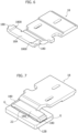
- Figure 1 is exemplary of a power semiconductor device 10 with a plastic package.
- the device 10 comprises a substrate (leadframe) 12 having arranged thereon one or more semiconductor chips or dice.
- a substrate laminated structure
- the terms chip/s and die/dice are regarded as synonymous.
- the figures illustrate by way of example a semiconductor power device 10 comprising a low-power section (e.g., a controller die 141) attached on a first die pad 121A in the leadframe 12 and a high-power section (e.g., one or more power dice 142) attached on one or more die pads 122A in the lead frame 12, with an array of leads 12B around the die pads 121A, 122A having the dice 141 and 142 mounted thereon.
- a low-power section e.g., a controller die 141
- a high-power section e.g., one or more power dice 142
- leadframe (or “lead frame”) is currently used (see, for instance the USPC Consolidated Glossary of the United States Patent and Trademark Office) to indicate a metal frame that provides support for an integrated circuit chip or die as well as electrical leads to interconnect the integrated circuit in the die or chip to other electrical components or contacts.
- a leadframe comprises an array of electrically-conductive formations (or leads, e.g., 12B) that from an outline location extend inwardly in the direction of a semiconductor chip or die (e.g., 141, 142) thus forming an array of electrically-conductive formations from a die pad (e.g., 121A, 122A) configured to have at least one semiconductor chip or die attached thereon.
- a die attach adhesive 1420 a die attach film or DAF, for instance.
- a device 10 as illustrated in Figure 1 is intended to be mounted on a substrate such as a printed circuit board (PCB - not visible in the figures), using solder material, for instance.
- a substrate such as a printed circuit board (PCB - not visible in the figures), using solder material, for instance.
- Electrically conductive formations are provided to electrically couple the semiconductor chip(s) 141, 142 to selected ones of the leads (outer pads) 12B in the leadframe 12.
- these electrically conductive formations comprise wire bonding patterns 16 coupling the low-power section (chip 141) to selected ones of the leads 12B and to the high-power section (chip or chips 142. These wire bonding patterns 16 are coupled to die pads 1410 provided at the front or top surfaces of the chips 141 and 142.
- clips 18 are used to couple the high-power section (chip or chips 142) to selected ones of the leads 12B acting as (power) output pads of the device 10.
- wires such as the wires 16 are still used to provide electrical coupling to a low-power section (e.g., a controller) in the device.
- An insulating encapsulation 20 (e.g., an epoxy resin) is molded on the assembly thus formed to complete the plastic body of the device 10.
- While the device 10 as shown comprises two clips 18, certain devices may comprise just one clip or more than two clips.
- producing the device 10 as discussed herein involves:
- the electrically conductive clip 18 has coupling surfaces facing towards the semiconductor chip 142 and the electrically conductive pad 12B.
- the electrically conductive clip 18 positioned in said bridge-like position is soldered to the semiconductor chip 142 and to the electrically conductive pad 12B to provide electrical coupling therebetween.
- soldering is via soldering material 22 dispensed (in a manner known per se to those of skill in the art) at said coupling surfaces.
- the soldering material 22 is consolidated (in a manner likewise known per se to those of skill in the art), e.g., via heat treatment in an oven.
- clips such as the clip 18 are placed using a clip attach equipment and a solder paste 22 is used to connect the clip to pad and die. Solder curing in an oven is applied to provide a solid connection of the clips 18 to pad (e.g., 12B) and die (e.g., 142).
- the thickness of the solder 22 and the tendency of the clip to "float" on the solder 22 in a fluid state may also lie at the basis of undesired excessive clip tilt.
- Selecting solder paste materials different from those conventionally used may have negative effects in terms of thermal and electrical performance.
- the clip or clips 18 are immobilized in the desired bridge-like position via welding (e.g., laser welding) or gluing at one or more dedicated immobilization areas, e.g., as generally indicated by 180 in Figure 1 .
- the immobilization areas 180 can be suitably formed and shaped, e.g., by coining, in order to be configured to facilitate welding or gluing of the clip(s) 18.
- Examples as considered herein are thus based on the concept of "tacking” or “basting” the coupling of the clip(s) 18 to chip(s) 142 and the pad(s) or lead(s) 12B in the desired bridge-like position so that the clip(s) are immobilized and retained in such a position during soldering, thus countering undesired displacement (e.g., translation/rotation/tilt) .
- this involves stepped lateral portions of a clip 18 resting on the leadframe 12 (e.g., at a lead or pad 12B) and providing flat areas of contact for the laser welding or the gluing of the clip 18.
- Figures 3 to 6 are exemplary of the possibility of modifying a clip 18 as illustrated in Figures 1 and 2 in such a way to facilitate "tacking” or “basting” the coupling of the clip(s) 18 by laser welding as exemplified by references LB in Figure 3 .
- Figures 7 to 9 are exemplary of the possibility of modifying a clip 18 as illustrated in Figures 1 and 2 at the areas or regions 180 in such a way to facilitate "tacking” or “basting” the coupling of the clip(s) 18 by gluing as exemplified by the reference G in Figure 7 .
- solder material 22 is provided to facilitate electrical coupling of the clip 18 to the lead 12B.
- the clip 18 can be pre-fixed through laser welding after clip attach to the clip bar.
- Such micro-welding facilitates robust clip positioning until the solder paste 22, after melting, carries out the brazing.
- the clip(s) 18 maintain the die 141 well placed during reflow avoiding translation and rotation.
- Flat welding areas 180 at the clip edges also facilitate clip planarity, which results in improved results in board-level testing (BLT) as compared with conventional processes.
- Glue drops as indicated by reference G in Figure 7 can be dispensed on a leadframe clip bar in addition to solder paste, with glue curing taking place during preheating in a reflow tunnel oven. Such gluing facilitates robust clip positioning until the solder paste 22, after melting, carries out the brazing.
- glue bonded clip(s) 18 maintain the die 141 well placed during reflow.
- clips such as the clips 18 exhibit (in manner known per se) a bent shape with a distal portion 18A configured to be coupled to the lead(s) 12B and thus at least slightly downset to allow for the thickness of the chip 142.
- the dedicated "tacking" or “basting” (laser welding, gluing) areas 180 are provided at such distal portion 18A.
- a pair of such areas 180 are provided at opposed ends of the distal portion 18A.
- the area(s) 180 at least slightly protrude from the general plane of the (distal portion 18A of) clip 18. This results in containment walls (indicated by reference 1800 in Figures 4, 5 , 6 , 8, and 9 ) being formed that facilitate containment of solder paste 22 as visible in Figures 3 and 7 .
- solder paste 22 in a molten state can penetrate into such a gap to provide a solder layer of controlled thickness.
- the shape of the areas 180 was not found to represent per se a critical parameter.
- dedicated welding/gluing areas 180 are shown formed at the clip end 18A intended to cooperate with a pad/lead 12B in the leadframe 12.
- such areas 180 could be formed also or only at the opposed end of the clip 18, that is at the end intended to cooperate with the chip 141
Landscapes
- Physics & Mathematics (AREA)
- Optics & Photonics (AREA)
- Engineering & Computer Science (AREA)
- Plasma & Fusion (AREA)
- Mechanical Engineering (AREA)
- Die Bonding (AREA)
Abstract

Description
- The description relates to semiconductor devices.
- One or more embodiments can be applied advantageously to power semiconductor devices.
- Various types of semiconductor devices with a plastic package comprise:
- a substrate (leadframe) having one or more semiconductor chips or dice arranged thereon,
- electrically conductive formations (wires, ribbons, clips) coupling the semiconductor chip(s) to leads (outer pads) in the substrate, and
- an insulating encapsulation (e.g., a resin) molded on the assembly thus formed to complete the plastic body of the device.
- In a power semiconductor device, the current transferred from the high-power section to the output pads of the device can be significant and ribbons or clips are used for that purpose in the place of wires. Wires can still be used to provide electrical coupling to a low-power section (e.g., a controller) in the device.
- Ribbons are placed using essentially a wire bonder process.
- Clips are placed with a clip attach equipment, and a solder paste is used to connect the clip to pad and die. Solder curing in an oven is applied to provide a solid connection of clips to pad and die.
- Conventional clip attachment equipment facilitates achieving an adequate accuracy in chip placement as the clip is applied on die and pad, after which the assembly is transferred to an oven for solder curing.
- During this handling and curing process, clips may become displaced from a desired correct position. This may result in a defective final product. Solder thickness and the tendency of the clip to "float" on solder in a fluid state may also lie at the basis of undesired excessive clip tilt.
- Documents
JP 3 314768 B2 DE 11 2020 001100 T5 orJP 5 857361 B2 - An object of one or more embodiments is to contribute in adequately addressing the issues discussed in the foregoing.
- According to one or more embodiments, such an object can be achieved via a method having the features set forth in the claims that follow.
- One or more embodiments may relate to a corresponding semiconductor device.
- The claims are an integral part of the technical teaching on the embodiments as provided herein.
- One or more embodiments may provide one or more of the following advantages:
- accurate clip positioning is facilitated throughout the assembly process with undesired movement (e.g., rotation) effectively countered, and
- solder thickness can be adequately controlled.
- One or more embodiments will now be described, by way of example only, with reference to the annexed figures, wherein:
-
Figure 1 is a perspective view of a power semiconductor device, -
Figure 2 is a sectional view along line II-II ofFigure 1 , -
Figure 3 illustrates a possible way of implementing embodiments of the present description in elements (clips) of a device as illustrated inFigures 1 and 2 , -
Figure 4 is a perspective view of the modified element ofFigure 3 , shown in isolation, -
Figure 5 is a view of the portion ofFigure 4 indicated by arrow V, reproduced on an enlarged scale, -
Figure 6 is a perspective view of the element illustrated inFigure 4 observed from a different viewpoint, -
Figure 7 illustrates another possible way of implementing embodiments of the present description in elements (clips) of a device as illustrated inFigures 1 and 2 , -
Figure 8 is a perspective view of the modified element ofFigure 3 , shown in isolation, and -
Figure 9 is a perspective view of the element illustrated inFigure 7 observed from a different viewpoint. - Corresponding numerals and symbols in the different figures generally refer to corresponding parts unless otherwise indicated.
- The figures are drawn to clearly illustrate the relevant aspects of the embodiments and are not necessarily drawn to scale.
- The edges of features drawn in the figures do not necessarily indicate the termination of the extent of the feature.
- In the ensuing description one or more specific details are illustrated, aimed at providing an in-depth understanding of examples of embodiments of this description. The embodiments may be obtained without one or more of the specific details, or with other methods, components, materials, etc. In other cases, known structures, materials, or operations are not illustrated or described in detail so that certain aspects of embodiments will not be obscured.
- Reference to "an embodiment" or "one embodiment" in the framework of the present description is intended to indicate that a particular configuration, structure, or characteristic described in relation to the embodiment is comprised in at least one embodiment. Hence, phrases such as "in an embodiment" or "in one embodiment" that may be present in one or more points of the present description do not necessarily refer to one and the same embodiment.
- Moreover, particular conformations, structures, or characteristics may be combined in any adequate way in one or more embodiments.
- The headings/references used herein are provided merely for convenience and hence do not define the extent of protection or the scope of the embodiments.
- For simplicity and ease of explanation, throughout this description, like parts or elements are indicated in the various figures with like reference signs, and a corresponding description will not be repeated for each and every figure.
- In current manufacturing processes of semiconductor devices, plural devices are manufactured concurrently to be separated into single individual device in a final singulation. For simplicity and ease of explanation, the following description will refer to manufacturing a single device.
-
Figure 1 is exemplary of apower semiconductor device 10 with a plastic package. - As conventional in the art, the
device 10 comprises a substrate (leadframe) 12 having arranged thereon one or more semiconductor chips or dice. As used herein, the terms chip/s and die/dice are regarded as synonymous. - The figures illustrate by way of example a
semiconductor power device 10 comprising a low-power section (e.g., a controller die 141) attached on afirst die pad 121A in theleadframe 12 and a high-power section (e.g., one or more power dice 142) attached on one ormore die pads 122A in thelead frame 12, with an array ofleads 12B around thedie pads dice - The designation "leadframe" (or "lead frame") is currently used (see, for instance the USPC Consolidated Glossary of the United States Patent and Trademark Office) to indicate a metal frame that provides support for an integrated circuit chip or die as well as electrical leads to interconnect the integrated circuit in the die or chip to other electrical components or contacts.
- Essentially, a leadframe comprises an array of electrically-conductive formations (or leads, e.g., 12B) that from an outline location extend inwardly in the direction of a semiconductor chip or die (e.g., 141, 142) thus forming an array of electrically-conductive formations from a die pad (e.g., 121A, 122A) configured to have at least one semiconductor chip or die attached thereon. This may be via conventional means such as a die attach adhesive 1420 (a die attach film or DAF, for instance).
- A
device 10 as illustrated inFigure 1 is intended to be mounted on a substrate such as a printed circuit board (PCB - not visible in the figures), using solder material, for instance. - Electrically conductive formations are provided to electrically couple the semiconductor chip(s) 141, 142 to selected ones of the leads (outer pads) 12B in the
leadframe 12. - As illustrated, these electrically conductive formations comprise
wire bonding patterns 16 coupling the low-power section (chip 141) to selected ones of theleads 12B and to the high-power section (chip orchips 142. Thesewire bonding patterns 16 are coupled to diepads 1410 provided at the front or top surfaces of thechips - Conversely, so-called
clips 18 are used to couple the high-power section (chip or chips 142) to selected ones of theleads 12B acting as (power) output pads of thedevice 10. - Using
clips 18 in the place of wires as included in the wire bonding patterns 16 (used to provide electrical coupling to a low-power section e.g., a controller 141) takes into account the fact that the current transferred from the high-power section 142 to the output pads in a power semiconductor device may be significant. As noted, wires such as thewires 16 are still used to provide electrical coupling to a low-power section (e.g., a controller) in the device. - An insulating encapsulation 20 (e.g., an epoxy resin) is molded on the assembly thus formed to complete the plastic body of the
device 10. - While the
device 10 as shown comprises twoclips 18, certain devices may comprise just one clip or more than two clips. - A device structure as discussed so far is conventional in the art, which makes it unnecessary to provide a more detailed description herein.
- To summarize, for the purposes herein, producing the
device 10 as discussed herein involves: - arranging at least one
semiconductor chip 142 on a die pad 12A in asubstrate 12 that comprises at least one electricallyconductive pad 12B by (that is, adjacent or sidewise) the die pad 12A, and - positioning at least one electrically
conductive clip 18 in a bridge-like position between the at least onesemiconductor chip 142 and the at least one electricallyconductive pad 12B. - In such a bridge-like position, the electrically
conductive clip 18 has coupling surfaces facing towards thesemiconductor chip 142 and the electricallyconductive pad 12B. - The electrically
conductive clip 18 positioned in said bridge-like position is soldered to thesemiconductor chip 142 and to the electricallyconductive pad 12B to provide electrical coupling therebetween. - As illustrated, soldering is via soldering
material 22 dispensed (in a manner known per se to those of skill in the art) at said coupling surfaces. Thesoldering material 22 is consolidated (in a manner likewise known per se to those of skill in the art), e.g., via heat treatment in an oven. - As discussed, clips such as the
clip 18 are placed using a clip attach equipment and asolder paste 22 is used to connect the clip to pad and die. Solder curing in an oven is applied to provide a solid connection of theclips 18 to pad (e.g., 12B) and die (e.g., 142). - Conventional clip attachment equipment facilitates achieving an adequate accuracy in chip placement as a
clip 18 is applied bridge-like between a die such as thedie 142 and a respective pad/lead such as the pad/lead 12A: this case is considered for simplicity; in certain devices anindividual clip 18 may be coupled, e.g., to plural pads/leads. - After clip placement the assembly is transferred to an oven for solder curing. During this handling and curing process clips may become displaced from a desired correct position, which may result in a defective final product.
- The thickness of the
solder 22 and the tendency of the clip to "float" on thesolder 22 in a fluid state may also lie at the basis of undesired excessive clip tilt. - Undesired clip movement (displacement) can be attempted to be countered by adding fixing features in the clip and leadframe design.
- Smooth handling may also help along with very accurate clip centering in clip placement.
- Selecting solder paste materials countering undesired clip floating properties can also be considered.
- None of these solutions appears fully satisfactory, for various reasons.
- For instance, certain features added to the clip/leadframe design can be space-consuming, which may suggest reducing pad dimensions and/or using larger package dimensions to gain space, neither of which is attractive/desirable.
- Handling of the parts involved is already fairly gentle and further improvements in that directions are hardly conceivable.
- Selecting solder paste materials different from those conventionally used may have negative effects in terms of thermal and electrical performance.
- In examples as considered herein - prior to soldering- the clip or clips 18 are immobilized in the desired bridge-like position via welding (e.g., laser welding) or gluing at one or more dedicated immobilization areas, e.g., as generally indicated by 180 in
Figure 1 . - As discussed in the following, the
immobilization areas 180 can be suitably formed and shaped, e.g., by coining, in order to be configured to facilitate welding or gluing of the clip(s) 18. - Examples as considered herein are thus based on the concept of "tacking" or "basting" the coupling of the clip(s) 18 to chip(s) 142 and the pad(s) or lead(s) 12B in the desired bridge-like position so that the clip(s) are immobilized and retained in such a position during soldering, thus countering undesired displacement (e.g., translation/rotation/tilt) .
- In various examples this involves stepped lateral portions of a
clip 18 resting on the leadframe 12 (e.g., at a lead orpad 12B) and providing flat areas of contact for the laser welding or the gluing of theclip 18. -
Figures 3 to 6 are exemplary of the possibility of modifying aclip 18 as illustrated inFigures 1 and 2 in such a way to facilitate "tacking" or "basting" the coupling of the clip(s) 18 by laser welding as exemplified by references LB inFigure 3 . -
Figures 7 to 9 are exemplary of the possibility of modifying aclip 18 as illustrated inFigures 1 and 2 at the areas orregions 180 in such a way to facilitate "tacking" or "basting" the coupling of the clip(s) 18 by gluing as exemplified by the reference G inFigure 7 . - In either case (laser welding, gluing) the fact is taken into account that solder
material 22 is provided to facilitate electrical coupling of theclip 18 to the lead 12B. - In order to avoid undesired detachment/displacement of the
clip 18 with respect to the desired bridge-like coupling position one or morededicated clip areas 180 to be used to apply (micro dot) laser welding LB -Figures 3 to 6 - or gluing G (via, e.g., the glue available under the trade designation Loctite® 3609 with Henkel AG& Co KGaA -Figures 7 to 9 . - In that way the
clip 18 can be pre-fixed through laser welding after clip attach to the clip bar. Such micro-welding facilitates robust clip positioning until thesolder paste 22, after melting, carries out the brazing. - Additionally, the clip(s) 18 maintain the die 141 well placed during reflow avoiding translation and rotation.
-
Flat welding areas 180 at the clip edges also facilitate clip planarity, which results in improved results in board-level testing (BLT) as compared with conventional processes. - Specific welding areas such as those indicated by the
reference 180 inFigures 3 to 6 can be realized (by coining, for instance) when manufacturing a clip bar. - The points above also apply identically to dedicated
clip areas 180 intended for gluing as represented inFigures 7 to 9 . - Glue drops as indicated by reference G in
Figure 7 can be dispensed on a leadframe clip bar in addition to solder paste, with glue curing taking place during preheating in a reflow tunnel oven. Such gluing facilitates robust clip positioning until thesolder paste 22, after melting, carries out the brazing. - Additionally, glue bonded clip(s) 18 maintain the die 141 well placed during reflow.
- Improved clip planarity is again facilitated as compared with conventional processes.
- In both instances (laser welding, gluing) clip and die are maintained in a desired position during assembly processes.
- As illustrated, throughout the figures, clips such as the
clips 18 exhibit (in manner known per se) a bent shape with adistal portion 18A configured to be coupled to the lead(s) 12B and thus at least slightly downset to allow for the thickness of thechip 142. - Advantageously, the dedicated "tacking" or "basting" (laser welding, gluing)
areas 180 are provided at suchdistal portion 18A. - Advantageously, a pair of
such areas 180 are provided at opposed ends of thedistal portion 18A. - As visible in figures such as
Figure 4 orFigure 8 , the area(s) 180 at least slightly protrude from the general plane of the (distal portion 18A of)clip 18. This results in containment walls (indicated byreference 1800 inFigures 4, 5 ,6 ,8, and 9 ) being formed that facilitate containment ofsolder paste 22 as visible inFigures 3 and7 . - In that way, once the area(s) 180 are fixed (welded or glued) to the lead 12B, a gap is formed between the remainder of the
distal portion 18A and the lead 12B. - As visible in figures such as
Figure 3 orFigure 7 ,solder paste 22 in a molten state can penetrate into such a gap to provide a solder layer of controlled thickness. - The shape of the
areas 180 was not found to represent per se a critical parameter. - As illustrated in
Figures 3 to 6 , a round shape was however found to be advantageous forareas 180 intended for laser welding LB. - As illustrated in
Figures 7 to 9 , a rectangular (or square) shape was found to be advantageous forareas 180 intended for gluing G. - Examples as presented herein facilitate maintaining a precise clip "centering" during assembly processes.
- Undesired clip movement and rotation are avoided, and solder thickness can be adequately controlled.
- In examples as presented herein, dedicated welding/gluing
areas 180 are shown formed at theclip end 18A intended to cooperate with a pad/lead 12B in theleadframe 12. - In principle (at least insofar as gluing is concerned)
such areas 180 could be formed also or only at the opposed end of theclip 18, that is at the end intended to cooperate with thechip 141 - It is noted that the presence of the dedicated welding/gluing
areas 180 will be noticeable also in the final device, where the clip(s) 18 will be fixed in the desired bridge-like position by the joint action of: - the
solder material 22, and - laser welds (recognizable as such) or masses of glue as used to immobilize the clip during soldering.
- Without prejudice to the underlying principles, the details and embodiments may vary, even significantly, with respect to what has been described by way of example only without departing from the extent of protection.
- The extent of protection is determined by the annexed claims.
Claims (14)
- A method, comprising:arranging at least one semiconductor chip (142) on a die pad (12A) in a substrate (12), the substrate (12) comprising at least one electrically conductive pad (12B) by the die pad (12A),positioning at least one electrically conductive clip (18) in a bridge-like position between the at least one semiconductor chip (142) and the at least one electrically conductive pad (12B), wherein, in said bridge-like position, the at least one electrically conductive clip (18) has coupling surfaces facing towards the at least one semiconductor chip (142) and the at least one electrically conductive pad (12B), andsoldering (22) the at least one electrically conductive clip (18) in said bridge-like position to the at least one semiconductor chip (142) and to the at least one electrically conductive pad (12B) to provide electrical coupling therebetween, wherein soldering is via soldering material (22) at said coupling surfaces,wherein the method comprises, prior to said soldering, immobilizing (LB, G) the at least one electrically conductive clip (18) in said bridge-like position via welding (LB) or gluing (G) to at least one of the electrically conductive pads (12B) and the at least one semiconductor chip (142).
- The method of claim 1, wherein said welding is laser welding (LB).
- The method of claim 1, wherein immobilizing is by gluing (G) via glue (G) dispensed concurrently with said soldering material (22).
- The method of any of the previous claims, comprising providing in the at least one electrically conductive clip (18), preferably by coining, at least one dedicated immobilization area (180) configured for said welding (LB) or gluing (G).
- The method of claim 4, wherein the at least one dedicated immobilization area (180) protrudes from the at least one electrically conductive clip (18) forming a lateral containment wall (1800) for said soldering material (22).
- The method of claim 4 or claim 5, wherein the at least one dedicated immobilization area (180) is planar, preferably of a round or quadrangular shape.
- The method of any of claims 4 to 6, comprising providing the least one dedicated immobilization area (180) in a, preferably downset, distal portion (18A) of the at least one electrically conductive clip (18).
- The method of claim 7, comprising providing a pair of dedicated immobilization areas (180) at opposed ends of said distal portion (18A) of the at least one electrically conductive clip (18).
- A device (10), comprising:at least one semiconductor chip (142) on a die pad (12A) in a substrate (12), the substrate (12) comprising at least one electrically conductive pad (12B) by the die pad (12A),at least one electrically conductive clip (18) positioned in a bridge-like position between the at least one semiconductor chip (142) and the at least one electrically conductive pad (12B), the at least one electrically conductive clip (18) having coupling surfaces facing towards the at least one semiconductor (142) and the at least one electrically conductive pad (12B), andsolder material (22) applied at said coupling surfaces of the at least one electrically conductive clip (18) in said bridge-like position, the solder material (22) electrically coupling the at least one electrically conductive clip (18) to the at least one semiconductor chip (142) and to the at least one electrically conductive pad (12B),wherein the at least one electrically conductive clip (18) is fixed in said bridge-like position to at least one of the electrically conductive pads (12B) and the at least one semiconductor chip (142) via welding, preferably laser welding (LB), or gluing (G) in addition to said solder material (22).
- The device (10) of claim 9, wherein the at least one electrically conductive clip (18) comprises at least one dedicated immobilization area (180) having welding (LB) or gluing (G) applied thereto.
- The device (10) of claim 10, wherein the at least one dedicated immobilization area (180):protrudes from the at least one electrically conductive clip (18) forming a lateral containment wall (1800) for said soldering material (22), and/oris planar, preferably of a round or quadrangular shape.
- The device (10) of claim 10 or claim 11, wherein the least one dedicated immobilization area (180) is provided in a, preferably downset, distal portion (18A) of the at least one electrically conductive clip (18).
- The device (10) of claim 12, comprising a pair of dedicated immobilization areas (180) at opposed ends of said distal portion (18A) of the at least one electrically conductive clip (18).
- The device (10) of any of claims 9 to 13, wherein the device is a power semiconductor device with the at least one electrically conductive clip (18) sized and dimensioned to carry high currents produced by the at least one semiconductor chip (142).
Applications Claiming Priority (1)
| Application Number | Priority Date | Filing Date | Title |
|---|---|---|---|
| IT102022000001649A IT202200001649A1 (en) | 2022-02-01 | 2022-02-01 | Process for manufacturing semiconductor devices and corresponding semiconductor device |
Publications (2)
| Publication Number | Publication Date |
|---|---|
| EP4220693A1 true EP4220693A1 (en) | 2023-08-02 |
| EP4220693B1 EP4220693B1 (en) | 2024-11-06 |
Family
ID=80999859
Family Applications (1)
| Application Number | Title | Priority Date | Filing Date |
|---|---|---|---|
| EP23153889.3A Active EP4220693B1 (en) | 2022-02-01 | 2023-01-30 | Method of manufacturing a semiconductor device and corresponding semiconductor device |
Country Status (4)
| Country | Link |
|---|---|
| US (1) | US20230245955A1 (en) |
| EP (1) | EP4220693B1 (en) |
| CN (2) | CN219591387U (en) |
| IT (1) | IT202200001649A1 (en) |
Cited By (1)
| Publication number | Priority date | Publication date | Assignee | Title |
|---|---|---|---|---|
| US12538809B2 (en) | 2022-02-01 | 2026-01-27 | Stmicroelectronics S.R.L | Method of manufacturing semiconductor devices and corresponding semiconductor device |
Families Citing this family (2)
| Publication number | Priority date | Publication date | Assignee | Title |
|---|---|---|---|---|
| IT202200001649A1 (en) * | 2022-02-01 | 2023-08-01 | St Microelectronics Srl | Process for manufacturing semiconductor devices and corresponding semiconductor device |
| IT202200024687A1 (en) | 2022-11-30 | 2024-05-30 | St Microelectronics Int Nv | Process for producing semiconductor devices and corresponding semiconductor device |
Citations (3)
| Publication number | Priority date | Publication date | Assignee | Title |
|---|---|---|---|---|
| JP3314768B2 (en) | 1999-10-26 | 2002-08-12 | サンケン電気株式会社 | Semiconductor device and manufacturing method thereof |
| JP5857361B2 (en) | 2011-02-15 | 2016-02-10 | 新電元工業株式会社 | Semiconductor device |
| DE112020001100T5 (en) | 2019-03-05 | 2022-01-05 | Rohm Co., Ltd. | SEMICONDUCTOR COMPONENT AND BOND PROCESS |
Family Cites Families (10)
| Publication number | Priority date | Publication date | Assignee | Title |
|---|---|---|---|---|
| TW200733272A (en) * | 2005-11-01 | 2007-09-01 | Koninkl Philips Electronics Nv | Methods of packaging a semiconductor die and die package formed by the methods |
| US8035221B2 (en) * | 2007-11-08 | 2011-10-11 | Intersil Americas, Inc. | Clip mount for integrated circuit leadframes |
| US8581376B2 (en) * | 2010-03-18 | 2013-11-12 | Alpha & Omega Semiconductor Incorporated | Stacked dual chip package and method of fabrication |
| EP2930747A1 (en) * | 2014-04-07 | 2015-10-14 | Nxp B.V. | Lead for connection to a semiconductor device |
| JP6578900B2 (en) * | 2014-12-10 | 2019-09-25 | 株式会社デンソー | Semiconductor device and manufacturing method thereof |
| US11742266B2 (en) * | 2019-12-12 | 2023-08-29 | Texas Instruments Incorporated | Electronic device topside cooling |
| US20230170322A1 (en) * | 2021-11-29 | 2023-06-01 | Texas Instruments Incorporated | Gang clip with mount compound arrester |
| IT202200001646A1 (en) * | 2022-02-01 | 2023-08-01 | St Microelectronics Srl | Process for manufacturing semiconductor devices and corresponding semiconductor device |
| IT202200001649A1 (en) * | 2022-02-01 | 2023-08-01 | St Microelectronics Srl | Process for manufacturing semiconductor devices and corresponding semiconductor device |
| IT202200024687A1 (en) * | 2022-11-30 | 2024-05-30 | St Microelectronics Int Nv | Process for producing semiconductor devices and corresponding semiconductor device |
-
2022
- 2022-02-01 IT IT102022000001649A patent/IT202200001649A1/en unknown
-
2023
- 2023-01-26 US US18/101,983 patent/US20230245955A1/en active Pending
- 2023-01-30 EP EP23153889.3A patent/EP4220693B1/en active Active
- 2023-01-31 CN CN202320090404.9U patent/CN219591387U/en active Active
- 2023-01-31 CN CN202310047032.6A patent/CN116544124A/en active Pending
Patent Citations (3)
| Publication number | Priority date | Publication date | Assignee | Title |
|---|---|---|---|---|
| JP3314768B2 (en) | 1999-10-26 | 2002-08-12 | サンケン電気株式会社 | Semiconductor device and manufacturing method thereof |
| JP5857361B2 (en) | 2011-02-15 | 2016-02-10 | 新電元工業株式会社 | Semiconductor device |
| DE112020001100T5 (en) | 2019-03-05 | 2022-01-05 | Rohm Co., Ltd. | SEMICONDUCTOR COMPONENT AND BOND PROCESS |
Cited By (1)
| Publication number | Priority date | Publication date | Assignee | Title |
|---|---|---|---|---|
| US12538809B2 (en) | 2022-02-01 | 2026-01-27 | Stmicroelectronics S.R.L | Method of manufacturing semiconductor devices and corresponding semiconductor device |
Also Published As
| Publication number | Publication date |
|---|---|
| EP4220693B1 (en) | 2024-11-06 |
| IT202200001649A1 (en) | 2023-08-01 |
| US20230245955A1 (en) | 2023-08-03 |
| CN219591387U (en) | 2023-08-25 |
| CN116544124A (en) | 2023-08-04 |
Similar Documents
| Publication | Publication Date | Title |
|---|---|---|
| EP4220693B1 (en) | Method of manufacturing a semiconductor device and corresponding semiconductor device | |
| US5724726A (en) | Method of making leadframe for lead-on-chip (LOC) semiconductor device | |
| EP4220692A1 (en) | Method of manufacturing a semiconductor device and corresponding semiconductor device | |
| JPH09153586A (en) | Semiconductor device, manufacturing method thereof, and lead frame | |
| EP2922091B1 (en) | Leadless chip carrier | |
| KR20190084900A (en) | Semiconductor package and mehod for manufacturing the same | |
| US20020022304A1 (en) | Semiconductor device, method for fabricating the same, circuit board and electronic device | |
| EP4379788A1 (en) | A method of manufacturing semiconductor devices and corresponding semiconductor device | |
| KR100343150B1 (en) | Power semiconductor module with metal terminal, metal terminal manufacturing method of power semiconductor module, and power semiconductor module manufacturing method | |
| US20050287703A1 (en) | Multi-chip semiconductor connector assembly method | |
| JP2005311137A (en) | Semiconductor device and manufacturing method thereof, mounting structure of semiconductor device, and lead frame | |
| CN101553908A (en) | Folded frame carrier for MOSFET BGA | |
| JPH08148623A (en) | Semiconductor device | |
| EP4611023A1 (en) | Method of manufacturing semiconductor devices and corresponding device | |
| EP4517819A1 (en) | Method of manufacturing semiconductor devices, corresponding component and semiconductor device | |
| JPH11297729A (en) | Semiconductor package and method of forming the same | |
| CN120565420A (en) | Method for manufacturing a semiconductor device and corresponding device | |
| JP4750076B2 (en) | Manufacturing method of semiconductor device | |
| JP3419898B2 (en) | Semiconductor device and manufacturing method thereof | |
| JP2803334B2 (en) | Semiconductor device | |
| JPH01119045A (en) | Lead frame | |
| JPH05291739A (en) | Connecting terminal and connecting method for device using same | |
| JPS6199359A (en) | Hybrid integrated circuit device | |
| JPH04267385A (en) | Semiconductor module | |
| JPH08204062A (en) | Ball grid array type semiconductor device and method of manufacturing the same |
Legal Events
| Date | Code | Title | Description |
|---|---|---|---|
| PUAI | Public reference made under article 153(3) epc to a published international application that has entered the european phase |
Free format text: ORIGINAL CODE: 0009012 |
|
| STAA | Information on the status of an ep patent application or granted ep patent |
Free format text: STATUS: THE APPLICATION HAS BEEN PUBLISHED |
|
| AK | Designated contracting states |
Kind code of ref document: A1 Designated state(s): AL AT BE BG CH CY CZ DE DK EE ES FI FR GB GR HR HU IE IS IT LI LT LU LV MC ME MK MT NL NO PL PT RO RS SE SI SK SM TR |
|
| STAA | Information on the status of an ep patent application or granted ep patent |
Free format text: STATUS: REQUEST FOR EXAMINATION WAS MADE |
|
| 17P | Request for examination filed |
Effective date: 20240118 |
|
| RBV | Designated contracting states (corrected) |
Designated state(s): AL AT BE BG CH CY CZ DE DK EE ES FI FR GB GR HR HU IE IS IT LI LT LU LV MC ME MK MT NL NO PL PT RO RS SE SI SK SM TR |
|
| GRAP | Despatch of communication of intention to grant a patent |
Free format text: ORIGINAL CODE: EPIDOSNIGR1 |
|
| STAA | Information on the status of an ep patent application or granted ep patent |
Free format text: STATUS: GRANT OF PATENT IS INTENDED |
|
| INTG | Intention to grant announced |
Effective date: 20240621 |
|
| RIN1 | Information on inventor provided before grant (corrected) |
Inventor name: MARCHISI, FABIO Inventor name: MAZZOLA, MAURO |
|
| GRAS | Grant fee paid |
Free format text: ORIGINAL CODE: EPIDOSNIGR3 |
|
| GRAA | (expected) grant |
Free format text: ORIGINAL CODE: 0009210 |
|
| STAA | Information on the status of an ep patent application or granted ep patent |
Free format text: STATUS: THE PATENT HAS BEEN GRANTED |
|
| AK | Designated contracting states |
Kind code of ref document: B1 Designated state(s): AL AT BE BG CH CY CZ DE DK EE ES FI FR GB GR HR HU IE IS IT LI LT LU LV MC ME MK MT NL NO PL PT RO RS SE SI SK SM TR |
|
| REG | Reference to a national code |
Ref country code: GB Ref legal event code: FG4D |
|
| REG | Reference to a national code |
Ref country code: CH Ref legal event code: EP |
|
| REG | Reference to a national code |
Ref country code: DE Ref legal event code: R096 Ref document number: 602023000895 Country of ref document: DE |
|
| REG | Reference to a national code |
Ref country code: IE Ref legal event code: FG4D |
|
| REG | Reference to a national code |
Ref country code: LT Ref legal event code: MG9D |
|
| REG | Reference to a national code |
Ref country code: NL Ref legal event code: MP Effective date: 20241106 |
|
| PG25 | Lapsed in a contracting state [announced via postgrant information from national office to epo] |
Ref country code: HR Free format text: LAPSE BECAUSE OF FAILURE TO SUBMIT A TRANSLATION OF THE DESCRIPTION OR TO PAY THE FEE WITHIN THE PRESCRIBED TIME-LIMIT Effective date: 20241106 Ref country code: PT Free format text: LAPSE BECAUSE OF FAILURE TO SUBMIT A TRANSLATION OF THE DESCRIPTION OR TO PAY THE FEE WITHIN THE PRESCRIBED TIME-LIMIT Effective date: 20250306 Ref country code: IS Free format text: LAPSE BECAUSE OF FAILURE TO SUBMIT A TRANSLATION OF THE DESCRIPTION OR TO PAY THE FEE WITHIN THE PRESCRIBED TIME-LIMIT Effective date: 20250306 |
|
| PGFP | Annual fee paid to national office [announced via postgrant information from national office to epo] |
Ref country code: DE Payment date: 20241218 Year of fee payment: 3 |
|
| PG25 | Lapsed in a contracting state [announced via postgrant information from national office to epo] |
Ref country code: FI Free format text: LAPSE BECAUSE OF FAILURE TO SUBMIT A TRANSLATION OF THE DESCRIPTION OR TO PAY THE FEE WITHIN THE PRESCRIBED TIME-LIMIT Effective date: 20241106 Ref country code: NL Free format text: LAPSE BECAUSE OF FAILURE TO SUBMIT A TRANSLATION OF THE DESCRIPTION OR TO PAY THE FEE WITHIN THE PRESCRIBED TIME-LIMIT Effective date: 20241106 |
|
| REG | Reference to a national code |
Ref country code: AT Ref legal event code: MK05 Ref document number: 1740369 Country of ref document: AT Kind code of ref document: T Effective date: 20241106 |
|
| PG25 | Lapsed in a contracting state [announced via postgrant information from national office to epo] |
Ref country code: BG Free format text: LAPSE BECAUSE OF FAILURE TO SUBMIT A TRANSLATION OF THE DESCRIPTION OR TO PAY THE FEE WITHIN THE PRESCRIBED TIME-LIMIT Effective date: 20241106 |
|
| PG25 | Lapsed in a contracting state [announced via postgrant information from national office to epo] |
Ref country code: ES Free format text: LAPSE BECAUSE OF FAILURE TO SUBMIT A TRANSLATION OF THE DESCRIPTION OR TO PAY THE FEE WITHIN THE PRESCRIBED TIME-LIMIT Effective date: 20241106 |
|
| PG25 | Lapsed in a contracting state [announced via postgrant information from national office to epo] |
Ref country code: NO Free format text: LAPSE BECAUSE OF FAILURE TO SUBMIT A TRANSLATION OF THE DESCRIPTION OR TO PAY THE FEE WITHIN THE PRESCRIBED TIME-LIMIT Effective date: 20250206 |
|
| PG25 | Lapsed in a contracting state [announced via postgrant information from national office to epo] |
Ref country code: AT Free format text: LAPSE BECAUSE OF FAILURE TO SUBMIT A TRANSLATION OF THE DESCRIPTION OR TO PAY THE FEE WITHIN THE PRESCRIBED TIME-LIMIT Effective date: 20241106 Ref country code: LV Free format text: LAPSE BECAUSE OF FAILURE TO SUBMIT A TRANSLATION OF THE DESCRIPTION OR TO PAY THE FEE WITHIN THE PRESCRIBED TIME-LIMIT Effective date: 20241106 Ref country code: GR Free format text: LAPSE BECAUSE OF FAILURE TO SUBMIT A TRANSLATION OF THE DESCRIPTION OR TO PAY THE FEE WITHIN THE PRESCRIBED TIME-LIMIT Effective date: 20250207 |
|
| PG25 | Lapsed in a contracting state [announced via postgrant information from national office to epo] |
Ref country code: PL Free format text: LAPSE BECAUSE OF FAILURE TO SUBMIT A TRANSLATION OF THE DESCRIPTION OR TO PAY THE FEE WITHIN THE PRESCRIBED TIME-LIMIT Effective date: 20241106 |
|
| PG25 | Lapsed in a contracting state [announced via postgrant information from national office to epo] |
Ref country code: RS Free format text: LAPSE BECAUSE OF FAILURE TO SUBMIT A TRANSLATION OF THE DESCRIPTION OR TO PAY THE FEE WITHIN THE PRESCRIBED TIME-LIMIT Effective date: 20250206 |
|
| PG25 | Lapsed in a contracting state [announced via postgrant information from national office to epo] |
Ref country code: SM Free format text: LAPSE BECAUSE OF FAILURE TO SUBMIT A TRANSLATION OF THE DESCRIPTION OR TO PAY THE FEE WITHIN THE PRESCRIBED TIME-LIMIT Effective date: 20241106 |
|
| PG25 | Lapsed in a contracting state [announced via postgrant information from national office to epo] |
Ref country code: DK Free format text: LAPSE BECAUSE OF FAILURE TO SUBMIT A TRANSLATION OF THE DESCRIPTION OR TO PAY THE FEE WITHIN THE PRESCRIBED TIME-LIMIT Effective date: 20241106 |
|
| PG25 | Lapsed in a contracting state [announced via postgrant information from national office to epo] |
Ref country code: EE Free format text: LAPSE BECAUSE OF FAILURE TO SUBMIT A TRANSLATION OF THE DESCRIPTION OR TO PAY THE FEE WITHIN THE PRESCRIBED TIME-LIMIT Effective date: 20241106 |
|
| PG25 | Lapsed in a contracting state [announced via postgrant information from national office to epo] |
Ref country code: RO Free format text: LAPSE BECAUSE OF FAILURE TO SUBMIT A TRANSLATION OF THE DESCRIPTION OR TO PAY THE FEE WITHIN THE PRESCRIBED TIME-LIMIT Effective date: 20241106 |
|
| PG25 | Lapsed in a contracting state [announced via postgrant information from national office to epo] |
Ref country code: SK Free format text: LAPSE BECAUSE OF FAILURE TO SUBMIT A TRANSLATION OF THE DESCRIPTION OR TO PAY THE FEE WITHIN THE PRESCRIBED TIME-LIMIT Effective date: 20241106 |
|
| PG25 | Lapsed in a contracting state [announced via postgrant information from national office to epo] |
Ref country code: CZ Free format text: LAPSE BECAUSE OF FAILURE TO SUBMIT A TRANSLATION OF THE DESCRIPTION OR TO PAY THE FEE WITHIN THE PRESCRIBED TIME-LIMIT Effective date: 20241106 |
|
| PG25 | Lapsed in a contracting state [announced via postgrant information from national office to epo] |
Ref country code: IT Free format text: LAPSE BECAUSE OF FAILURE TO SUBMIT A TRANSLATION OF THE DESCRIPTION OR TO PAY THE FEE WITHIN THE PRESCRIBED TIME-LIMIT Effective date: 20241106 |
|
| REG | Reference to a national code |
Ref country code: DE Ref legal event code: R097 Ref document number: 602023000895 Country of ref document: DE |
|
| PG25 | Lapsed in a contracting state [announced via postgrant information from national office to epo] |
Ref country code: SE Free format text: LAPSE BECAUSE OF FAILURE TO SUBMIT A TRANSLATION OF THE DESCRIPTION OR TO PAY THE FEE WITHIN THE PRESCRIBED TIME-LIMIT Effective date: 20241106 |
|
| PLBE | No opposition filed within time limit |
Free format text: ORIGINAL CODE: 0009261 |
|
| STAA | Information on the status of an ep patent application or granted ep patent |
Free format text: STATUS: NO OPPOSITION FILED WITHIN TIME LIMIT |
|
| PG25 | Lapsed in a contracting state [announced via postgrant information from national office to epo] |
Ref country code: LU Free format text: LAPSE BECAUSE OF NON-PAYMENT OF DUE FEES Effective date: 20250130 Ref country code: MC Free format text: LAPSE BECAUSE OF FAILURE TO SUBMIT A TRANSLATION OF THE DESCRIPTION OR TO PAY THE FEE WITHIN THE PRESCRIBED TIME-LIMIT Effective date: 20241106 |
|
| 26N | No opposition filed |
Effective date: 20250807 |
|
| PG25 | Lapsed in a contracting state [announced via postgrant information from national office to epo] |
Ref country code: BE Free format text: LAPSE BECAUSE OF NON-PAYMENT OF DUE FEES Effective date: 20250131 |
|
| PG25 | Lapsed in a contracting state [announced via postgrant information from national office to epo] |
Ref country code: FR Free format text: LAPSE BECAUSE OF NON-PAYMENT OF DUE FEES Effective date: 20250131 |
|
| REG | Reference to a national code |
Ref country code: BE Ref legal event code: MM Effective date: 20250131 |
|
| REG | Reference to a national code |
Ref country code: DE Ref legal event code: R079 Ref document number: 602023000895 Country of ref document: DE Free format text: PREVIOUS MAIN CLASS: H01L0021600000 Ipc: H10W0070010000 |
|
| PG25 | Lapsed in a contracting state [announced via postgrant information from national office to epo] |
Ref country code: IE Free format text: LAPSE BECAUSE OF NON-PAYMENT OF DUE FEES Effective date: 20250130 |