EP4219401A1 - Oxide superconducting wire - Google Patents
Oxide superconducting wire Download PDFInfo
- Publication number
- EP4219401A1 EP4219401A1 EP21872044.9A EP21872044A EP4219401A1 EP 4219401 A1 EP4219401 A1 EP 4219401A1 EP 21872044 A EP21872044 A EP 21872044A EP 4219401 A1 EP4219401 A1 EP 4219401A1
- Authority
- EP
- European Patent Office
- Prior art keywords
- axis oriented
- layer
- superconducting
- superconducting layer
- substrate
- Prior art date
- Legal status (The legal status is an assumption and is not a legal conclusion. Google has not performed a legal analysis and makes no representation as to the accuracy of the status listed.)
- Granted
Links
Images

Classifications
-
- H—ELECTRICITY
- H01—ELECTRIC ELEMENTS
- H01B—CABLES; CONDUCTORS; INSULATORS; SELECTION OF MATERIALS FOR THEIR CONDUCTIVE, INSULATING OR DIELECTRIC PROPERTIES
- H01B12/00—Superconductive or hyperconductive conductors, cables, or transmission lines
- H01B12/02—Superconductive or hyperconductive conductors, cables, or transmission lines characterised by their form
- H01B12/06—Films or wires on bases or cores
-
- H—ELECTRICITY
- H10—SEMICONDUCTOR DEVICES; ELECTRIC SOLID-STATE DEVICES NOT OTHERWISE PROVIDED FOR
- H10N—ELECTRIC SOLID-STATE DEVICES NOT OTHERWISE PROVIDED FOR
- H10N60/00—Superconducting devices
- H10N60/20—Permanent superconducting devices
- H10N60/203—Permanent superconducting devices comprising high-Tc ceramic materials
-
- H—ELECTRICITY
- H10—SEMICONDUCTOR DEVICES; ELECTRIC SOLID-STATE DEVICES NOT OTHERWISE PROVIDED FOR
- H10N—ELECTRIC SOLID-STATE DEVICES NOT OTHERWISE PROVIDED FOR
- H10N60/00—Superconducting devices
- H10N60/80—Constructional details
- H10N60/85—Superconducting active materials
- H10N60/855—Ceramic superconductors
-
- H—ELECTRICITY
- H10—SEMICONDUCTOR DEVICES; ELECTRIC SOLID-STATE DEVICES NOT OTHERWISE PROVIDED FOR
- H10N—ELECTRIC SOLID-STATE DEVICES NOT OTHERWISE PROVIDED FOR
- H10N60/00—Superconducting devices
- H10N60/80—Constructional details
-
- Y—GENERAL TAGGING OF NEW TECHNOLOGICAL DEVELOPMENTS; GENERAL TAGGING OF CROSS-SECTIONAL TECHNOLOGIES SPANNING OVER SEVERAL SECTIONS OF THE IPC; TECHNICAL SUBJECTS COVERED BY FORMER USPC CROSS-REFERENCE ART COLLECTIONS [XRACs] AND DIGESTS
- Y02—TECHNOLOGIES OR APPLICATIONS FOR MITIGATION OR ADAPTATION AGAINST CLIMATE CHANGE
- Y02E—REDUCTION OF GREENHOUSE GAS [GHG] EMISSIONS, RELATED TO ENERGY GENERATION, TRANSMISSION OR DISTRIBUTION
- Y02E40/00—Technologies for an efficient electrical power generation, transmission or distribution
- Y02E40/60—Superconducting electric elements or equipment; Power systems integrating superconducting elements or equipment
Definitions
- the present invention relates to an oxide superconducting wire.
- Patent Document 1 discloses an oxide superconducting wire having a laminated structure that includes an intermediate layer, a superconducting layer, and a protective layer successively laminated on a substrate.
- Patent Literature 1 Japanese Unexamined Patent Application, First Publication, No. 2014-110125
- connection resistance at the connection part increases, and there is a problem in that joule heat is generated at the connection part.
- the connection resistance due to solder connecting is predominant in an interlayer resistance between a superconducting layer and a protective layer, and it is important to reduce the interlayer resistance in order to reduce the joule heat.
- connection resistance increases there is a problem in that a bypass current is less likely to flow from the superconducting layer to the protective layer when bypassing the current during quenching.
- the invention is made in light of the above-described circumstances, and the objective thereof is to provide an oxide superconducting wire with a reduced interlayer resistance between a superconducting layer and a protective layer.
- an oxide superconducting wire includes a substrate having a main surface, a superconducting layer provided above the substrate and formed of a rare-earth high-temperature superconductor, and a protective layer provided on the superconducting layer and in contact with the superconducting layer.
- the superconducting layer includes a-axis oriented grains having an a-axis oriented in a direction perpendicular to the main surface of the substrate.
- An a-axis oriented grain ratio expressing a proportion of the a-axis oriented grains to the entirety of crystal grains forming the superconducting layer is in a range of 4.1 to 11.9%.
- a superconducting layer provided above the substrate does not only means that a superconducting layer is provided on the substrate but also means that a superconducting layer base body is provided above the substrate in a configuration in which an intermediate layer film or the like is disposed between the superconducting layer and the substrate.
- the inventors have discovered that it is possible to achieve a reduction in the interlayer resistance between the superconducting layer and the protective layer by forming the superconducting layer such that a proportion of a-axis oriented grains to the entirety of the crystal grains of the superconducting layer is 4.1 to 11.9%, and hence arriving at the invention.
- an oxide superconducting wire having a reduced interlayer resistance between the superconducting layer and the protective layer By preparing a plurality of the oxide superconducting wires and solder-connecting the oxide superconducting wires adjacent to each other, it is possible to produce a long superconducting wire having a reduced connection resistance.
- the a-axis oriented grain ratio may be less than or equal to 8.2%.
- an oxide superconducting wire includes a substrate having a main surface, a first superconducting layer provided above the substrate and formed of a rare-earth high-temperature superconductor, a second superconducting layer provided above the first superconducting layer and formed of a rare-earth high-temperature superconductor, and a protective layer provided on the second superconducting layer and in contact with the second superconducting layer.
- the second superconducting layer includes a-axis oriented grains having an a-axis oriented in a direction perpendicular to the main surface of the substrate.
- An a-axis oriented grain ratio expressing a proportion of the a-axis oriented grains to the entirety of crystal grains forming the second superconducting layer is in a range of 4.1 to 11.9%.
- an oxide superconducting wire having a reduced interlayer resistance between the second superconducting layer and the protective layer By preparing a plurality of the oxide superconducting wires and solder-connecting the oxide superconducting wires adjacent to each other, it is possible to produce a long superconducting wire having a reduced connection resistance.
- the first superconducting layer includes first a-axis oriented grains serving as a-axis oriented grains having an a-axis oriented in a direction perpendicular to the main surface of the substrate.
- the second superconducting layer includes second a-axis oriented grains serving as a-axis oriented grains having an a-axis oriented in a direction perpendicular to the main surface of the substrate.
- An a-axis oriented grain ratio expressing a proportion of the first a-axis oriented grains to the entirety of crystal grains forming the first superconducting layer is defined as a first ratio
- an a-axis oriented grain ratio expressing a proportion of the second a-axis oriented grains to the entirety of crystal grains forming the second superconducting layer is defined as a second ratio.
- the first ratio is lower than the second ratio.
- the oxide superconducting wire 1A includes a substrate 10, an intermediate layer 11 provided on the substrate 10, a superconducting layer 12 provided on the intermediate layer 11, a protective layer 13 provided on the superconducting layer 12, and a stabilizing layer 14 provided on the protective layer 13.
- the oxide superconducting wire 1A may include an insulating coating layer that covers the substrate 10, the intermediate layer 11, the superconducting layer 12, the protective layer 13, and the stabilizing layer 14.
- a height of the oxide superconducting wire 1A in other words, a length from a bottom surface of the substrate 10 to the upper surface of the protective layer 13 (the length in the up-down direction in FIG. 1 ) is, for example, 80 ⁇ m.
- a width of the oxide superconducting wire 1A in other words, a length from a left end to a right end of the oxide superconducting wire 1A (the length in the left-right direction in FIG. 1 ) is, for example, 12mm.
- the substrate 10 is a tape-shaped metal substrate.
- metals forming the metal substrate a nickel alloy typified by hastelloy (registered trademark), stainless steel, an oriented Ni-W alloy having a texture introduced into the nickel alloy, or the like.
- the intermediate layer 11 may have a multi- layered structure, and for example, may have a diffusion-preventing layer, a bed layer, an orientation layer, a cap layer, or the like in order from the substrate 10 to the superconducting layer 12.
- the number of each layer is not limited to one.
- a layer of the above-described layers forming the intermediate layer 11 may be omitted.
- a configuration including two or more layers having the same type repeatedly stacked may be adopted.
- the intermediate layer 11 may be metal oxide.
- the superconducting layer 12 has a function of allowing a current to flow thereto when being in a superconducting state.
- the superconducting layer 12 is formed of a rare-earth high-temperature superconductor and is provided so as to be in contact with the protective layer 13.
- an oxide superconductor having generally-known compositions can be widely used, and a Y-based superconductor, a copper oxide superconductor such as a Bi-based superconductor, or the like is adopted.
- REBa 2 Cu 3 O 7-x As a composition of the Y-based superconductor, for example, such as REBa 2 Cu 3 O 7-x (“RE” refers to rare earth elements such as Y, La, Nd, Sm, Er, Gd, or the like, and "x" refers to oxygen defect is adopted.
- RE refers to rare earth elements such as Y, La, Nd, Sm, Er, Gd, or the like
- x refers to oxygen defect
- Y123 (YBa 2 Cu 3 O 7-x ) and Gd123 (GdBa 2 Cu 3 O 7-x ) are adopted.
- Bi 2 Sr 2 Ca n-1 Cu n O 4+2n+ ⁇ (n” refers to the number of layers of CuO 2 , and " ⁇ " refers to the excess oxygen) is adopted.
- the oxide superconductor has an insulator serving as a mother material, the oxide superconductor has oriented crystal structures and possesses properties showing superconducting characteristics by causing oxygen to be incorporated into the oxide superconductor by oxygen annealing treatment.
- the superconducting layer 12 includes a-axis oriented grains serving as crystalline grains having an a-axis oriented in a direction perpendicular to the main surface of the substrate 10.
- a Cu-O surface on which a current is likely to flow thereon in a superconducting state is present so as to be perpendicular to the main surface of the substrate.
- the superconducting layer 12 including the a-axis oriented grains has an excellent quantum binding property at a crystal grain boundary between the a-axis oriented grains, and the superconducting characteristics are not almost degraded at the crystal grain boundary. Consequently, in the superconducting layer 12, electricity is likely to flow in the a-axis direction.
- a proportion (a-axis oriented grain ratio Xa) of the a-axis oriented grains included in superconducting layer 12 to the entirety (100%) of the crystalline grains forming the superconducting layer 12 is in a range of 4.1 to 11.9%. Furthermore, it is preferable that the a-axis oriented grain ratio Xa be less than or equal to 8.2% in the range.
- a-axis oriented grain ratio Xa By adjusting conditions such as a film deposition temperature, a film formation rate (film-formation speed), or the like when forming the superconducting layer 12, it is possible to control the a-axis oriented grain ratio Xa to be a desired value in the aforementioned range.
- the protective layer 13 is a current path that functions as a bypass route through which an overcurrent flows due to some accidents when a current is being applied to the oxide superconducting wire 1A. It is preferable that the protective layer 13 be formed of Ag or a material containing at least Ag. Furthermore, a material used to form the protective layer 13 may be a composite or an alloy containing noble metal such as Au, Pt, or the like, and or a plurality of the materials mentioned above may be used therefor.
- the stabilizing layer 14 As a material used for the stabilizing layer 14, copper, a Cu-Zn alloy (brass), a copper alloy such as a Cu-Ni alloy, aluminum, an aluminum alloy, stainless steel, or the like is selected.
- the stabilizing layer 14 may be configured of a plurality of layers. Moreover, the stabilizing layer 14 may be formed by metallic plating. The stabilizing layer 14 may have a configuration in which the entirety of a multi-layered body including the substrate 10, the protective layer 13, and a layer located between the substrate 10 and the protective layer 13 is coated with a plating layer.
- the superconducting layer 12 in contact with the protective layer 13 includes the a-axis oriented grains having the a-axis oriented in the direction perpendicular to the main surface of the substrate, and includes the a-axis oriented grains. Accordingly, the Cu-O surface serving as a superconducting current path is present so as to be perpendicular to the main surface of the substrate 10. Since the a-axis is oriented in the direction perpendicular to the main surface of the substrate 10, a low-value resistance is obtained in the direction perpendicular to the main surface of the substrate, and a current is likely to flow therein.
- the a-axis oriented grain ratio Xa is set in a range of 4.1 to 11.9% as described hereinbelow, the effect of reducing an interlayer resistance between the superconducting layer 12 and the protective layer 13 is obtained. Furthermore, by setting the a-axis oriented grain ratio Xa to be less than or equal to 8.2%, it is possible to not only reduce an interlayer resistance but also to suppress a reduction in a critical current density in a longitudinal direction of the oxide superconducting wire 1A. Note that, in the explanation described below, the critical current density of the longitudinal direction of the oxide superconducting wire is simply referred to as the critical current density.
- a superconducting layer is formed such that a Cu-O surface is present in a direction parallel to a main surface of a substrate.
- a current is less likely to flow in a direction perpendicular to the main surface of the substrate.
- the proportion (a-axis oriented grain ratio Xa) of the a-axis oriented grains having the a-axis oriented in the direction perpendicular to the main surface of the substrate 10 is optimized, therefore, an amount of a current path the mutually flows between the superconducting layer 12 and the protective layer 13 increases, and it is possible to reduce the interlayer resistance.
- the oxide superconducting wire 1B according to the embodiment is different from the oxide superconducting wire 1A according to the above-mentioned first embodiment in that a superconducting layer is configured of two layers (a first superconducting layer and a second superconducting layer).
- FIG. 2 identical reference numerals are used for the elements which are identical to those of the first embodiment, and the explanations thereof are omitted or simplified here.
- the oxide superconducting wire 1B includes the substrate 10, the intermediate layer 11 provided on the substrate 10, a first superconducting layer 12A provided on the intermediate layer 11, a second superconducting layer 12B provided on the first superconducting layer 12A, the protective layer 13 provided on the second superconducting layer 12B, and the stabilizing layer 14 provided on the protective layer 13.
- the oxide superconducting wire 1B include an insulating coating layer that covers the substrate 10, the intermediate layer 11, the first superconducting layer 12A, the second superconducting layer 12B, the protective layer 13, and the stabilizing layer 14.
- Each of the first superconducting layer 12A and the second superconducting layer 12B is formed of a rare-earth high-temperature superconductor.
- the first superconducting layer 12A is formed on the intermediate layer 11 but is not in contact with the protective layer 13.
- the second superconducting layer 12B is formed on the first superconducting layer 12A and is in contact with the protective layer 13.
- a proportion (a-axis oriented grain ratio Xa2 of the second superconducting layer 12B, second ratio) of the a-axis oriented grains (second a-axis oriented grains) of the second superconducting layer 12B to the entirety of crystal grains forming the second superconducting layer 12B is in a range of 4.1 to 11.9% similar to the superconducting layer 12 according to the aforementioned first embodiment.
- a proportion (a-axis oriented grain ratio Xa1 of the first superconducting layer 12A, first ratio) of the a-axis oriented grains (first a-axis oriented grains) of the first superconducting layer 12A to the entirety of crystal grains forming the first superconducting layer 12A is less than the a-axis oriented grain ratio Xa2 of the second superconducting layer 12B.
- the a-axis oriented grain ratio Xa2 of the second superconducting layer 12B is 4.1%
- the a-axis oriented grain ratio Xa2 of the second superconducting layer 12B is 11.9%
- the a-axis oriented grain ratio Xa1 of the first superconducting layer 12A is only necessary to be less than 11.9%.
- the second superconducting layer 12B in contact with the protective layer 13 includes the a-axis oriented grains having the a-axis oriented in the direction perpendicular to the main surface of the substrate and includes the a-axis oriented grains, the Cu-O surface serving as a superconducting current path is present so as to be perpendicular to the main surface of the substrate. Since the a-axis is oriented in the direction perpendicular to the main surface of the substrate 10, a low-value resistance is obtained in the direction perpendicular to the main surface of the substrate, and a current is likely to flow therein.
- the a-axis oriented grain ratio Xa2 of the second superconducting layer 12B is set in a range of 4.1 to 11.9% as described hereinbelow, the effect of reducing an interlayer resistance between the second superconducting layer 12B and the protective layer 13 is obtained. Moreover, since the value of the a-axis oriented grain ratio Xa1 of the first superconducting layer 12A is lower than the value of the a-axis oriented grain ratio Xa2 of the second superconducting layer 12B, a proportion of grains having the a-axis or the b-axis oriented in a longitudinal direction of the oxide superconducting wire 1B is ensured.
- the oxide superconducting wire 1B includes two superconducting layers having the respective a-axis oriented grain ratios Xa1 and Xa2 different from each other, it is possible to obtain both effects of reducing an interlayer resistance and ensuring a critical current density.
- the number of layers forming the superconducting layer is two.
- a superconducting layer may be configured of three or more layers.
- the connected structure formed by using the oxide superconducting wire according to the above-mentioned embodiment of the invention includes a structure in which a plurality of the oxide superconducting wires 1A according to the first embodiment are solder-connected together.
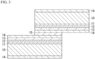
- FIG. 3 shows a connection portion at which two oxide superconducting wires are solder-connected together.
- a surface of the stabilizing layer 14 coating the protective layer 13 of one oxide superconducting wire faces a surface of the stabilizing layer 14 coating the protective layer 13 of the other oxide superconducting wire (the oxide superconducting wire located at a lower side in FIG. 3 ).
- the "one the oxide superconducting wire” may be referred to as a first oxide superconducting wire.
- the “the other oxide superconducting wire” may be referred to as a second oxide superconducting wire.
- the "one the oxide superconducting wire” and the “the other oxide superconducting wire” may be referred to as an "oxide superconducting wires overlapped to each other". Additionally, "oxide superconducting wires overlapped to each other” means that the oxide superconducting wires overlap each other in a thickness direction of the oxide superconducting wire.
- the stabilizing layer 14 located at an end portion of one oxide superconducting wire is electrically connected to the stabilizing layer 14 located at an end portion of the other of oxide superconducting wire via solder 15.
- each of the two oxide superconducting wires is connected to a different oxide superconducting wire via solder.
- an electrical connected structure using the solder 15 shown in FIG. 3 is adopted. That is, a long oxide superconducting wire having a plurality of oxide superconducting wires that are solder-connected together in the extending direction of the oxide superconducting wire is obtained.
- a plurality of the oxide superconducting wires 1B according to the second embodiment may be prepared instead of the plurality of the oxide superconducting wires 1A according to the first embodiment, and the oxide superconducting wires 1B overlapping each other may be solder-connected together as shown in FIG. 3 . Also in this case, it is possible to produce a long superconducting wire having a reduced connection resistance and ensuring the critical current density.
- a superconducting layer is only necessary to be provided above a substrate, the superconducting layer may be provided on the substrate, or the superconducting layer may be directly in contact with the substrate.
- Table 1 shows the evaluation results of a critical current density ratio, an interlayer resistance ratio (R ratio), and an interlayer resistance R ratio regarding Experimental Examples 1 to 9 having a-axis oriented grain ratios Xa (%, a proportion of the a-axis oriented grains to the entirety of crystal grains forming a superconducting layer) different from each other.
- a measurement method and a calculation method of the a-axis oriented grain ratio Xa, the critical current density ratio, and the interlayer resistance ratio (R ratio), and the evaluation standards the interlayer resistance R ratio are as follows.
- Measurement of the a-axis oriented grain ratio Xa was carried out with respect to a sample (as depo) before being subjected to oxygen annealing.
- the a-axis oriented grain ratio Xa was measured by a ⁇ -2 ⁇ method of XRD.
- a count value at the (006) peak is defined as x
- a count value at the (200) peak is defined as y
- critical current density ratio (Jc ratio) represents a ratio with respect to the critical current density Jc of Experimental Example 1, that is, a proportion in the case in which the critical current density Jc of Experimental Example 1 is 1.
- An interlayer resistance R was measured in a state of a bridging connection in which the top surface and the back surface the wire are not replaced with each other.
- a connection length was 2 cm.
- measurement was carried out by applying Sn-Pb eutectic solder between bonding faces of two wires, overlapping the bonding faces each other, and pressing a heater against the portion at which the bonding faces overlaps each other.
- Interlayer Resistance Ratio represents a ratio with respect to the interlayer resistance of Experimental Example 1, that is, a proportion in the case in which the interlayer resistance of Experimental Example 1 is 1.
- the result “GOOD” means that the interlayer resistance R ratio was less than or equal to 0.7 and the evaluation result was good.
- the result “EXCELLENCE” means that the interlayer resistance R ratio was less than or equal to 0.5 and the evaluation result was excellent.
- the result “FAIL” means that the interlayer resistance R ratio exceeds 0.7 and the evaluation result was bad.
- the a-axis oriented grain ratio Xa2 of the second superconducting layer is set to be in a range of 4.1 to 11.9% and the a-axis oriented grain ratio Xa1 of the first superconducting layer is set to be less than or equal to 11.9%, it was apparent that the a-axis oriented grain ratio Xa1 of the first superconducting layer is preferably less than or equal to 8.2% in order to obtain a high degree of the critical current density.
- 1A, 1B ...oxide superconducting wire, 10...substrate, 11...intermediate layer, 12...superconducting layer, 12A...first superconducting layer (superconducting layer), 12B...second superconducting layer (superconducting layer), 13...protective layer, 14...stabilizing layer, 15...solder
Landscapes
- Chemical & Material Sciences (AREA)
- Engineering & Computer Science (AREA)
- Ceramic Engineering (AREA)
- Superconductors And Manufacturing Methods Therefor (AREA)
- Inorganic Compounds Of Heavy Metals (AREA)
Abstract
Description
- The present invention relates to an oxide superconducting wire.
- This application claims priority from
Japanese Patent Application No. 2020-160613, filed September 25, 2020 - Patent Document 1 discloses an oxide superconducting wire having a laminated structure that includes an intermediate layer, a superconducting layer, and a protective layer successively laminated on a substrate.
- Conventionally, to produce a superconducting wire having a length of several kilometers, a plurality of short superconducting wires are connected together by soldering.
- [Patent Literature 1]
Japanese Unexamined Patent Application, First Publication, No. 2014-110125 - However, when oxide superconducting wires are solder-connected, connection resistance at the connection part increases, and there is a problem in that joule heat is generated at the connection part. Specifically, the connection resistance due to solder connecting is predominant in an interlayer resistance between a superconducting layer and a protective layer, and it is important to reduce the interlayer resistance in order to reduce the joule heat. Furthermore, when connection resistance increases, there is a problem in that a bypass current is less likely to flow from the superconducting layer to the protective layer when bypassing the current during quenching.
- The invention is made in light of the above-described circumstances, and the objective thereof is to provide an oxide superconducting wire with a reduced interlayer resistance between a superconducting layer and a protective layer.
- To resolve the problem presented above, an oxide superconducting wire according to an aspect of the invention includes a substrate having a main surface, a superconducting layer provided above the substrate and formed of a rare-earth high-temperature superconductor, and a protective layer provided on the superconducting layer and in contact with the superconducting layer. The superconducting layer includes a-axis oriented grains having an a-axis oriented in a direction perpendicular to the main surface of the substrate. An a-axis oriented grain ratio expressing a proportion of the a-axis oriented grains to the entirety of crystal grains forming the superconducting layer is in a range of 4.1 to 11.9%.
- Here, the term "a superconducting layer provided above the substrate" does not only means that a superconducting layer is provided on the substrate but also means that a superconducting layer base body is provided above the substrate in a configuration in which an intermediate layer film or the like is disposed between the superconducting layer and the substrate.
- Conventionally, in a crystal configuration of an oriented superconducting layer having crystals oriented in an a-axis, a b-axis, and a c-axis, it is known that the c-axis of crystal grains is often oriented in a direction perpendicular to the main surface of the substrate. In contrast, the inventors have discovered that, of the crystal grains forming a superconducting layer, a-axis oriented grains having the a-axis oriented in a direction perpendicular to the main surface of the substrate have an effect on an interlayer resistance between the superconducting layer and the protective layer. Furthermore, as a result of intensive research, the inventors have discovered that it is possible to achieve a reduction in the interlayer resistance between the superconducting layer and the protective layer by forming the superconducting layer such that a proportion of a-axis oriented grains to the entirety of the crystal grains of the superconducting layer is 4.1 to 11.9%, and hence arriving at the invention.
- According to an aspect of the invention, it is possible to produce an oxide superconducting wire having a reduced interlayer resistance between the superconducting layer and the protective layer. By preparing a plurality of the oxide superconducting wires and solder-connecting the oxide superconducting wires adjacent to each other, it is possible to produce a long superconducting wire having a reduced connection resistance.
- In the oxide superconducting wire according to the aspect of the invention, the a-axis oriented grain ratio may be less than or equal to 8.2%.
- With this configuration, it is possible to not only reduce an interlayer resistance but also to ensure a critical current density in a longitudinal direction of the oxide superconducting wire.
- To resolve the problem presented above, an oxide superconducting wire according to an aspect of the invention includes a substrate having a main surface, a first superconducting layer provided above the substrate and formed of a rare-earth high-temperature superconductor, a second superconducting layer provided above the first superconducting layer and formed of a rare-earth high-temperature superconductor, and a protective layer provided on the second superconducting layer and in contact with the second superconducting layer. The second superconducting layer includes a-axis oriented grains having an a-axis oriented in a direction perpendicular to the main surface of the substrate. An a-axis oriented grain ratio expressing a proportion of the a-axis oriented grains to the entirety of crystal grains forming the second superconducting layer is in a range of 4.1 to 11.9%.
- According to an aspect of the invention, it is possible to produce an oxide superconducting wire having a reduced interlayer resistance between the second superconducting layer and the protective layer. By preparing a plurality of the oxide superconducting wires and solder-connecting the oxide superconducting wires adjacent to each other, it is possible to produce a long superconducting wire having a reduced connection resistance.
- In the oxide superconducting wire according to the aspect of the invention, the first superconducting layer includes first a-axis oriented grains serving as a-axis oriented grains having an a-axis oriented in a direction perpendicular to the main surface of the substrate. The second superconducting layer includes second a-axis oriented grains serving as a-axis oriented grains having an a-axis oriented in a direction perpendicular to the main surface of the substrate. An a-axis oriented grain ratio expressing a proportion of the first a-axis oriented grains to the entirety of crystal grains forming the first superconducting layer is defined as a first ratio, and an a-axis oriented grain ratio expressing a proportion of the second a-axis oriented grains to the entirety of crystal grains forming the second superconducting layer is defined as a second ratio. In this case, the first ratio is lower than the second ratio.
- With this configuration, it is possible to reduce an interlayer resistance between the superconducting layer and the protective layer by the second superconducting layer, and it is possible to not only reduce an interlayer resistance but also to ensure a critical current density in a longitudinal direction of the oxide superconducting wire by the first superconducting layer. In other words, by providing the oxide superconducting wire including two superconducting layers having a-axis oriented grain ratios different from each other, it is possible to obtain both effects of reducing an interlayer resistance and ensuring a critical current density in the longitudinal direction of the oxide superconducting wire.
- According to the aforementioned aspects of the invention, it is possible to reduce an interlayer resistance between a superconducting layer and a protective layer.
-
-
FIG. 1 is an enlarged cross-sectional view showing an oxide superconducting wire according to a first embodiment of the invention. -
FIG. 2 is an enlarged cross-sectional view showing an oxide superconducting wire according to a second embodiment of the invention. -
FIG. 3 is a view showing a connected structure formed using an oxide superconducting wire according to an embodiment of the invention and is an enlarged cross-sectional view showing a connected structure having solder-connected two wires of a plurality of oxide superconducting wires. - Hereinafter, an oxide superconducting wire according to an embodiment of the invention will be described in detail with reference to the drawings. In the drawings used in the description, the relevant portions of the invention may be enlarged, for convenience, in order to make the features thereof easier to understand, and the dimension ratios and the like for each of the components are not necessarily the same as those in reality.
- First, an oxide superconducting wire according to a first embodiment will be described with reference to
FIG. 1 . - The oxide
superconducting wire 1A according to the embodiment includes asubstrate 10, anintermediate layer 11 provided on thesubstrate 10, asuperconducting layer 12 provided on theintermediate layer 11, aprotective layer 13 provided on thesuperconducting layer 12, and a stabilizinglayer 14 provided on theprotective layer 13. The oxidesuperconducting wire 1A may include an insulating coating layer that covers thesubstrate 10, theintermediate layer 11, thesuperconducting layer 12, theprotective layer 13, and the stabilizinglayer 14. - A height of the oxide
superconducting wire 1A, in other words, a length from a bottom surface of thesubstrate 10 to the upper surface of the protective layer 13 (the length in the up-down direction inFIG. 1 ) is, for example, 80 µm. - A width of the oxide
superconducting wire 1A, in other words, a length from a left end to a right end of the oxidesuperconducting wire 1A (the length in the left-right direction inFIG. 1 ) is, for example, 12mm. - The
substrate 10 is a tape-shaped metal substrate. As specific examples of metals forming the metal substrate, a nickel alloy typified by hastelloy (registered trademark), stainless steel, an oriented Ni-W alloy having a texture introduced into the nickel alloy, or the like. - The
intermediate layer 11 may have a multi- layered structure, and for example, may have a diffusion-preventing layer, a bed layer, an orientation layer, a cap layer, or the like in order from thesubstrate 10 to thesuperconducting layer 12. In a configuration having the above-described layers provided in theintermediate layer 11, the number of each layer is not limited to one. A layer of the above-described layers forming theintermediate layer 11 may be omitted. Furthermore, a configuration including two or more layers having the same type repeatedly stacked may be adopted. Theintermediate layer 11 may be metal oxide. By forming thesuperconducting layer 12 on theintermediate layer 11 having excellent orientation, it is possible to easily obtain thesuperconducting layer 12 having excellent orientation. - The
superconducting layer 12 has a function of allowing a current to flow thereto when being in a superconducting state. - The
superconducting layer 12 is formed of a rare-earth high-temperature superconductor and is provided so as to be in contact with theprotective layer 13. - Specifically, as a material used for the
superconducting layer 12, an oxide superconductor having generally-known compositions can be widely used, and a Y-based superconductor, a copper oxide superconductor such as a Bi-based superconductor, or the like is adopted. - As a composition of the Y-based superconductor, for example, such as REBa2Cu3O7-x ("RE" refers to rare earth elements such as Y, La, Nd, Sm, Er, Gd, or the like, and "x" refers to oxygen defect is adopted.
- As a specific composition of the Y-based superconductor, Y123 (YBa2Cu3O7-x) and Gd123 (GdBa2Cu3O7-x) are adopted.
- As a composition of the Bi-based superconductor, for example, Bi2Sr2Can-1CunO4+2n+δ ("n" refers to the number of layers of CuO2, and "δ" refers to the excess oxygen) is adopted. Although the oxide superconductor has an insulator serving as a mother material, the oxide superconductor has oriented crystal structures and possesses properties showing superconducting characteristics by causing oxygen to be incorporated into the oxide superconductor by oxygen annealing treatment.
- Moreover, the
superconducting layer 12 includes a-axis oriented grains serving as crystalline grains having an a-axis oriented in a direction perpendicular to the main surface of thesubstrate 10. In the a-axis oriented grains, a Cu-O surface on which a current is likely to flow thereon in a superconducting state is present so as to be perpendicular to the main surface of the substrate. Thesuperconducting layer 12 including the a-axis oriented grains has an excellent quantum binding property at a crystal grain boundary between the a-axis oriented grains, and the superconducting characteristics are not almost degraded at the crystal grain boundary. Consequently, in thesuperconducting layer 12, electricity is likely to flow in the a-axis direction. A proportion (a-axis oriented grain ratio Xa) of the a-axis oriented grains included insuperconducting layer 12 to the entirety (100%) of the crystalline grains forming thesuperconducting layer 12 is in a range of 4.1 to 11.9%. Furthermore, it is preferable that the a-axis oriented grain ratio Xa be less than or equal to 8.2% in the range. - By adjusting conditions such as a film deposition temperature, a film formation rate (film-formation speed), or the like when forming the
superconducting layer 12, it is possible to control the a-axis oriented grain ratio Xa to be a desired value in the aforementioned range. - The
protective layer 13 is a current path that functions as a bypass route through which an overcurrent flows due to some accidents when a current is being applied to theoxide superconducting wire 1A. It is preferable that theprotective layer 13 be formed of Ag or a material containing at least Ag. Furthermore, a material used to form theprotective layer 13 may be a composite or an alloy containing noble metal such as Au, Pt, or the like, and or a plurality of the materials mentioned above may be used therefor. - As a material used for the stabilizing
layer 14, copper, a Cu-Zn alloy (brass), a copper alloy such as a Cu-Ni alloy, aluminum, an aluminum alloy, stainless steel, or the like is selected. - The stabilizing
layer 14 may be configured of a plurality of layers. Moreover, the stabilizinglayer 14 may be formed by metallic plating. The stabilizinglayer 14 may have a configuration in which the entirety of a multi-layered body including thesubstrate 10, theprotective layer 13, and a layer located between thesubstrate 10 and theprotective layer 13 is coated with a plating layer. - Next, actions and effects of the
oxide superconducting wire 1A having the above-described configuration will be described. - The
superconducting layer 12 in contact with theprotective layer 13 includes the a-axis oriented grains having the a-axis oriented in the direction perpendicular to the main surface of the substrate, and includes the a-axis oriented grains. Accordingly, the Cu-O surface serving as a superconducting current path is present so as to be perpendicular to the main surface of thesubstrate 10. Since the a-axis is oriented in the direction perpendicular to the main surface of thesubstrate 10, a low-value resistance is obtained in the direction perpendicular to the main surface of the substrate, and a current is likely to flow therein. Particularly, since the a-axis oriented grain ratio Xa is set in a range of 4.1 to 11.9% as described hereinbelow, the effect of reducing an interlayer resistance between thesuperconducting layer 12 and theprotective layer 13 is obtained. Furthermore, by setting the a-axis oriented grain ratio Xa to be less than or equal to 8.2%, it is possible to not only reduce an interlayer resistance but also to suppress a reduction in a critical current density in a longitudinal direction of theoxide superconducting wire 1A. Note that, in the explanation described below, the critical current density of the longitudinal direction of the oxide superconducting wire is simply referred to as the critical current density. - On the other hand, in conventional oxide superconducting wires, in general, a superconducting layer is formed such that a Cu-O surface is present in a direction parallel to a main surface of a substrate. In this situation, since a c-axis of a crystalline grain is oriented in a direction perpendicular to the main surface of the substrate, a current is less likely to flow in a direction perpendicular to the main surface of the substrate.
- In contrast, according to the embodiment, the proportion (a-axis oriented grain ratio Xa) of the a-axis oriented grains having the a-axis oriented in the direction perpendicular to the main surface of the
substrate 10 is optimized, therefore, an amount of a current path the mutually flows between thesuperconducting layer 12 and theprotective layer 13 increases, and it is possible to reduce the interlayer resistance. - Next, an oxide superconducting wire according to a second embodiment will be described with reference to
FIG. 2 . - The
oxide superconducting wire 1B according to the embodiment is different from theoxide superconducting wire 1A according to the above-mentioned first embodiment in that a superconducting layer is configured of two layers (a first superconducting layer and a second superconducting layer). - In
FIG. 2 , identical reference numerals are used for the elements which are identical to those of the first embodiment, and the explanations thereof are omitted or simplified here. - The
oxide superconducting wire 1B according to the embodiment includes thesubstrate 10, theintermediate layer 11 provided on thesubstrate 10, afirst superconducting layer 12A provided on theintermediate layer 11, asecond superconducting layer 12B provided on thefirst superconducting layer 12A, theprotective layer 13 provided on thesecond superconducting layer 12B, and the stabilizinglayer 14 provided on theprotective layer 13. Theoxide superconducting wire 1B include an insulating coating layer that covers thesubstrate 10, theintermediate layer 11, thefirst superconducting layer 12A, thesecond superconducting layer 12B, theprotective layer 13, and the stabilizinglayer 14. - Each of the
first superconducting layer 12A and thesecond superconducting layer 12B is formed of a rare-earth high-temperature superconductor. Thefirst superconducting layer 12A is formed on theintermediate layer 11 but is not in contact with theprotective layer 13. Thesecond superconducting layer 12B is formed on thefirst superconducting layer 12A and is in contact with theprotective layer 13. - A proportion (a-axis oriented grain ratio Xa2 of the
second superconducting layer 12B, second ratio) of the a-axis oriented grains (second a-axis oriented grains) of thesecond superconducting layer 12B to the entirety of crystal grains forming thesecond superconducting layer 12B is in a range of 4.1 to 11.9% similar to thesuperconducting layer 12 according to the aforementioned first embodiment. - On the other hand, A proportion (a-axis oriented grain ratio Xa1 of the
first superconducting layer 12A, first ratio) of the a-axis oriented grains (first a-axis oriented grains) of thefirst superconducting layer 12A to the entirety of crystal grains forming thefirst superconducting layer 12A is less than the a-axis oriented grain ratio Xa2 of thesecond superconducting layer 12B. - For example, when the a-axis oriented grain ratio Xa2 of the
second superconducting layer 12B is 4.1%, it is preferable that the a-axis oriented grain ratio Xa1 of thefirst superconducting layer 12A be less than 4.1%. - Additionally, when the a-axis oriented grain ratio Xa2 of the
second superconducting layer 12B is 11.9%, the a-axis oriented grain ratio Xa1 of thefirst superconducting layer 12A is only necessary to be less than 11.9%. However, since it is possible to obtain a high critical current density by setting the a-axis oriented grain ratio Xa to be less than or equal to 8.2%, it is preferable that the a-axis oriented grain ratio Xa1 of thefirst superconducting layer 12A be less than or equal to 8.2% in this case. - Next, actions and effects of the
oxide superconducting wire 1B having the above-described configuration will be described. - Since the
second superconducting layer 12B in contact with theprotective layer 13 includes the a-axis oriented grains having the a-axis oriented in the direction perpendicular to the main surface of the substrate and includes the a-axis oriented grains, the Cu-O surface serving as a superconducting current path is present so as to be perpendicular to the main surface of the substrate. Since the a-axis is oriented in the direction perpendicular to the main surface of thesubstrate 10, a low-value resistance is obtained in the direction perpendicular to the main surface of the substrate, and a current is likely to flow therein. Since the a-axis oriented grain ratio Xa2 of thesecond superconducting layer 12B is set in a range of 4.1 to 11.9% as described hereinbelow, the effect of reducing an interlayer resistance between thesecond superconducting layer 12B and theprotective layer 13 is obtained. Moreover, since the value of the a-axis oriented grain ratio Xa1 of thefirst superconducting layer 12A is lower than the value of the a-axis oriented grain ratio Xa2 of thesecond superconducting layer 12B, a proportion of grains having the a-axis or the b-axis oriented in a longitudinal direction of theoxide superconducting wire 1B is ensured. Consequently, it is possible to obtain a high critical current density in theoxide superconducting wire 1B. Specifically, it is possible to obtain a high critical current density by setting a value of the a-axis oriented grain ratio Xa1 of thefirst superconducting layer 12A to be less than or equal to 8.2%. - Accordingly, it is possible to reduce an interlayer resistance depending on increase in amount of a current path the mutually flows between the
second superconducting layer 12B and theprotective layer 13, and it is possible to ensure the critical current density of thefirst superconducting layer 12A. That is, since theoxide superconducting wire 1B includes two superconducting layers having the respective a-axis oriented grain ratios Xa1 and Xa2 different from each other, it is possible to obtain both effects of reducing an interlayer resistance and ensuring a critical current density. - In the aforementioned second embodiment, the number of layers forming the superconducting layer is two. As long as the a-axis oriented grain ratio Xa of the superconducting layer in contact with the protective layer is in a range of 4.1 to 11.9%, a superconducting layer may be configured of three or more layers.
- Next, a connected structure formed by using the oxide superconducting wire according to the above-mentioned embodiment of the invention will be described with reference to
FIG. 3 . - The connected structure formed by using the oxide superconducting wire according to the above-mentioned embodiment of the invention includes a structure in which a plurality of the
oxide superconducting wires 1A according to the first embodiment are solder-connected together. Particularly,FIG. 3 shows a connection portion at which two oxide superconducting wires are solder-connected together. - As shown in
FIG. 3 , a surface of the stabilizinglayer 14 coating theprotective layer 13 of one oxide superconducting wire (the oxide superconducting wire located at an upper side inFIG. 3 ) faces a surface of the stabilizinglayer 14 coating theprotective layer 13 of the other oxide superconducting wire (the oxide superconducting wire located at a lower side inFIG. 3 ). The "one the oxide superconducting wire" may be referred to as a first oxide superconducting wire. The "the other oxide superconducting wire" may be referred to as a second oxide superconducting wire. The "one the oxide superconducting wire" and the "the other oxide superconducting wire" may be referred to as an "oxide superconducting wires overlapped to each other". Additionally, "oxide superconducting wires overlapped to each other" means that the oxide superconducting wires overlap each other in a thickness direction of the oxide superconducting wire. - In this state, the stabilizing
layer 14 located at an end portion of one oxide superconducting wire is electrically connected to the stabilizinglayer 14 located at an end portion of the other of oxide superconducting wire viasolder 15. - Note that, although not shown in
FIG. 3 , the end portion of each of the two oxide superconducting wires is connected to a different oxide superconducting wire via solder. Also in the connected structure, an electrical connected structure using thesolder 15 shown inFIG. 3 is adopted. That is, a long oxide superconducting wire having a plurality of oxide superconducting wires that are solder-connected together in the extending direction of the oxide superconducting wire is obtained. - With this configuration, it is possible to produce the long oxide superconducting wire having a reduced connection resistance.
- Note that, a plurality of the
oxide superconducting wires 1B according to the second embodiment may be prepared instead of the plurality of theoxide superconducting wires 1A according to the first embodiment, and theoxide superconducting wires 1B overlapping each other may be solder-connected together as shown inFIG. 3 . Also in this case, it is possible to produce a long superconducting wire having a reduced connection resistance and ensuring the critical current density. - While preferred embodiments of the invention have been described and shown above, it should be understood that these are exemplary of the invention and are not to be considered as limiting. Additions, omissions, substitutions, and other modifications can be made without departing from the scope of the present invention. Accordingly, the invention is not to be considered as being limited by the foregoing description, and is only limited by the scope of the appended claims.
- In the above-described embodiments, the structure including the
intermediate layer 11 disposed between thesubstrate 10 and the superconducting layer 12 (first embodiment) and the structure including theintermediate layer 11 disposed between thesubstrate 10 and thefirst superconducting layer 12A (second embodiment) were described. - In the invention, a superconducting layer is only necessary to be provided above a substrate, the superconducting layer may be provided on the substrate, or the superconducting layer may be directly in contact with the substrate.
- Next, the invention will be specifically described with reference to Working Examples.
- Table 1 shows the evaluation results of a critical current density ratio, an interlayer resistance ratio (R ratio), and an interlayer resistance R ratio regarding Experimental Examples 1 to 9 having a-axis oriented grain ratios Xa (%, a proportion of the a-axis oriented grains to the entirety of crystal grains forming a superconducting layer) different from each other.
(Table 1) EXPERIMENTAL EXAMPLE A-AXIS ORIENTED GRAIN RATIO CRITICAL CURRENT DENSITY RATIO [Jc RATIO] INTERLAYER RESISTANCE RATIO [R RATIO] EVALUATION RESULT OF INTERLAYER RESISTANCE R RATIO 1 2.9 1 1 FAIL 2 3.3 0.97 0.78 FAIL 3 4.1 0.95 0.70 GOOD 4 5.4 0.92 0.68 GOOD 5 6.8 0.91 0.48 EXCELLENCE 6 8.2 0.85 0.43 EXCELLENCE 7 11.9 0.78 0.53 GOOD 8 27.1 0.11 0.74 FAIL 9 41.7 0 ∞ FAIL - A measurement method and a calculation method of the a-axis oriented grain ratio Xa, the critical current density ratio, and the interlayer resistance ratio (R ratio), and the evaluation standards the interlayer resistance R ratio are as follows.
- Measurement of the a-axis oriented grain ratio Xa was carried out with respect to a sample (as depo) before being subjected to oxygen annealing.
- The a-axis oriented grain ratio Xa was measured by a θ-2θ method of XRD. When a count value at the (006) peak is defined as x and a count value at the (200) peak is defined as y, the a-axis oriented grain ratio Xa was calculated by relational expression "(a-axis oriented grain ratio Xa (%)) = (100×y) / (x+y)".
- Regarding measurement and calculation of the critical current density Jc (77K, in self magnetic field), first, a sample after being subjected to oxygen annealing was prepared, and measurement values were obtained by a four-terminal method. The measurement values were divided by a thickness of a superconducting layer, and therefore the critical current densities Jc were obtained.
- In Table 1, "critical current density ratio (Jc ratio)" represents a ratio with respect to the critical current density Jc of Experimental Example 1, that is, a proportion in the case in which the critical current density Jc of Experimental Example 1 is 1.
- An interlayer resistance R was measured in a state of a bridging connection in which the top surface and the back surface the wire are not replaced with each other. A connection length was 2 cm. In the bridging connection, measurement was carried out by applying Sn-Pb eutectic solder between bonding faces of two wires, overlapping the bonding faces each other, and pressing a heater against the portion at which the bonding faces overlaps each other.
- In Table 1, "Interlayer Resistance Ratio (R Ratio)" represents a ratio with respect to the interlayer resistance of Experimental Example 1, that is, a proportion in the case in which the interlayer resistance of Experimental Example 1 is 1.
- In Table 1, the result "GOOD" means that the interlayer resistance R ratio was less than or equal to 0.7 and the evaluation result was good. The result "EXCELLENCE" means that the interlayer resistance R ratio was less than or equal to 0.5 and the evaluation result was excellent. In contrast, the result "FAIL" means that the interlayer resistance R ratio exceeds 0.7 and the evaluation result was bad.
- From the experimental result shown in Table 1, the following points were apparent.
- [1] In the case in which the a-axis oriented grain ratio Xa is in a range of 4.1 to 11.9%, the evaluation result of the interlayer resistance R ratio was good or excellent. Consequently, it was apparent that the interlayer resistance was reduced by setting the a-axis oriented grain ratio Xa of the superconducting layer to be in this range.
- [2] In contrast, in the case in which the a-axis oriented grain ratio Xa was less than 4.1% (3.3%, 2.9%) and in the case in which the a-axis oriented grain ratio Xa exceeds 11.9% (27.1%, 41.7%), the interlayer resistance ratio increases, and therefore the evaluation result of the interlayer resistance R ratio was bad. In this condition, it was apparent that a reduction in the interlayer resistance is not achieved.
Note that, although a current path in a vertical direction (a direction perpendicular to the main surface of the substrate) is obtained due to an increase in the a-axis oriented grain ratio Xa, the interlayer resistance ratio increases in the case in which the a-axis oriented grain ratio Xa exceeds 11.9%; it is conceivable that the reason for this is because the crystalline orientation of the superconducting layer becomes uneven due to overabundance of the a-axis oriented grains, other grains blocking a current are generated, the Cu-O surfaces thereof do not align, and a resistance increases. - [3] In the case in which the a-axis oriented grain ratio Xa is in a range of 4.1 to 11.9%, when the a-axis oriented grain ratio Xa was less than or equal to 8.2%, the critical current density ratio was greater than or equal to 0.85. For this reason, it was apparent the both effects of reducing an interlayer resistance and ensuring a critical current density are obtained.
- [4] In the case in which the a-axis oriented grain ratio Xa was less than or equal to 4.1%, the critical current density ratio was greater than or equal to 0.95. For this reason, in the configuration including the first superconducting layer not in contact with the protective layer and the second superconducting layer in contact with the protective layer, it was apparent the both effects of reducing an interlayer resistance and ensuring a critical current density are obtained by setting the a-axis oriented grain ratio Xa2 of the second superconducting layer to be in a range of 4.1 to 11.9% and setting the a-axis oriented grain ratio Xa1 of the first superconducting layer to be less than or equal to 4.1%.
- Note that, in the configuration including the first superconducting layer and the second superconducting layer, although it is conceivable that the a-axis oriented grain ratio Xa2 of the second superconducting layer is set to be in a range of 4.1 to 11.9% and the a-axis oriented grain ratio Xa1 of the first superconducting layer is set to be less than or equal to 11.9%, it was apparent that the a-axis oriented grain ratio Xa1 of the first superconducting layer is preferably less than or equal to 8.2% in order to obtain a high degree of the critical current density.
- 1A, 1B...oxide superconducting wire, 10...substrate, 11...intermediate layer, 12...superconducting layer, 12A...first superconducting layer (superconducting layer), 12B...second superconducting layer (superconducting layer), 13...protective layer, 14...stabilizing layer, 15...solder
Claims (4)
- An oxide superconducting wire comprising:a substrate having a main surface;a superconducting layer provided above the substrate and formed of a rare-earth high-temperature superconductor; anda protective layer provided on the superconducting layer and in contact with the superconducting layer; whereinthe superconducting layer includes a-axis oriented grains having an a-axis oriented in a direction perpendicular to the main surface of the substrate; andan a-axis oriented grain ratio expressing a proportion of the a-axis oriented grains to an entirety of crystal grains forming the superconducting layer is in a range of 4.1 to 11.9%.
- The oxide superconducting wire according to claim 1, wherein
the a-axis oriented grain ratio is less than or equal to 8.2%. - An oxide superconducting wire comprising:a substrate having a main surface;a first superconducting layer provided above the substrate and formed of a rare-earth high-temperature superconductor;a second superconducting layer provided above the first superconducting layer and formed of a rare-earth high-temperature superconductor; anda protective layer provided on the second superconducting layer and in contact with the second superconducting layer; whereinthe second superconducting layer includes a-axis oriented grains having an a-axis oriented in a direction perpendicular to the main surface of the substrate; andan a-axis oriented grain ratio expressing a proportion of the a-axis oriented grains to an entirety of crystal grains forming the second superconducting layer is in a range of 4.1 to 11.9%.
- The oxide superconducting wire according to claim 3, whereinthe first superconducting layer includes first a-axis oriented grains serving as a-axis oriented grains having an a-axis oriented in a direction perpendicular to the main surface of the substrate,the second superconducting layer includes second a-axis oriented grains serving as a-axis oriented grains having an a-axis oriented in a direction perpendicular to the main surface of the substrate, and whereinwhen an a-axis oriented grain ratio expressing a proportion of the first a-axis oriented grains to an entirety of crystal grains forming the first superconducting layer is defined as a first ratio and an a-axis oriented grain ratio expressing a proportion of the second a-axis oriented grains to an entirety of crystal grains forming the second superconducting layer is defined as a second ratio,the first ratio is lower than the second ratio.
Applications Claiming Priority (2)
| Application Number | Priority Date | Filing Date | Title |
|---|---|---|---|
| JP2020160613A JP6919042B1 (en) | 2020-09-25 | 2020-09-25 | Oxide superconducting wire |
| PCT/JP2021/030470 WO2022064912A1 (en) | 2020-09-25 | 2021-08-19 | Oxide superconducting wire |
Publications (3)
| Publication Number | Publication Date |
|---|---|
| EP4219401A1 true EP4219401A1 (en) | 2023-08-02 |
| EP4219401A4 EP4219401A4 (en) | 2024-10-16 |
| EP4219401B1 EP4219401B1 (en) | 2026-04-01 |
Family
ID=77172751
Family Applications (1)
| Application Number | Title | Priority Date | Filing Date |
|---|---|---|---|
| EP21872044.9A Active EP4219401B1 (en) | 2020-09-25 | 2021-08-19 | Oxide superconducting wire |
Country Status (5)
| Country | Link |
|---|---|
| US (1) | US12573527B2 (en) |
| EP (1) | EP4219401B1 (en) |
| JP (1) | JP6919042B1 (en) |
| CN (1) | CN116194408B (en) |
| WO (1) | WO2022064912A1 (en) |
Family Cites Families (16)
| Publication number | Priority date | Publication date | Assignee | Title |
|---|---|---|---|---|
| US6673387B1 (en) * | 2000-07-14 | 2004-01-06 | American Superconductor Corporation | Control of oxide layer reaction rates |
| JP4050730B2 (en) * | 2004-07-30 | 2008-02-20 | 株式会社東芝 | Oxide superconductor and manufacturing method thereof |
| CN102676993B (en) * | 2007-03-29 | 2015-03-04 | 株式会社藤仓 | Polycrystalline thin film and method for producing same and oxide superconductor |
| JP5427553B2 (en) * | 2009-10-30 | 2014-02-26 | 公益財団法人国際超電導産業技術研究センター | Base material for oxide superconducting conductor and method for producing the same, oxide superconducting conductor and method for producing the same |
| JP5757718B2 (en) * | 2010-10-27 | 2015-07-29 | 公益財団法人国際超電導産業技術研究センター | Manufacturing method of oxide superconducting wire |
| WO2012070631A1 (en) * | 2010-11-26 | 2012-05-31 | 古河電気工業株式会社 | Superconducting wire material and method for manufacturing superconducting wire material |
| JP2012204189A (en) * | 2011-03-25 | 2012-10-22 | Furukawa Electric Co Ltd:The | Method of manufacturing superconducting wire rod |
| JP2012204190A (en) * | 2011-03-25 | 2012-10-22 | Furukawa Electric Co Ltd:The | Oxide superconducting thin film |
| JP5894907B2 (en) | 2012-11-30 | 2016-03-30 | 株式会社フジクラ | Oxide superconducting wire and method for producing the same |
| JP6136073B2 (en) * | 2013-12-02 | 2017-05-31 | 住友電気工業株式会社 | Oxide superconducting thin film and manufacturing method thereof, and oxide superconducting thin film wire |
| JP6861633B2 (en) * | 2015-10-15 | 2021-04-21 | 住友電気工業株式会社 | Oxide superconducting wire |
| US10332656B2 (en) * | 2015-11-06 | 2019-06-25 | Fujikura Ltd. | Oxide superconducting wire |
| JP6359740B2 (en) * | 2017-09-11 | 2018-07-18 | 株式会社東芝 | Superconductor |
| RU2753187C1 (en) * | 2018-12-28 | 2021-08-12 | Фудзикура Лтд. | Superconducting oxide wire and method for its manufacturing |
| JP2020160613A (en) | 2019-03-25 | 2020-10-01 | オムロンヘルスケア株式会社 | Medication state management device, method, and program |
| US11100946B1 (en) * | 2020-07-01 | 2021-08-24 | Western Digital Technologies, Inc. | SOT differential reader and method of making same |
-
2020
- 2020-09-25 JP JP2020160613A patent/JP6919042B1/en active Active
-
2021
- 2021-08-19 CN CN202180065300.6A patent/CN116194408B/en active Active
- 2021-08-19 WO PCT/JP2021/030470 patent/WO2022064912A1/en not_active Ceased
- 2021-08-19 EP EP21872044.9A patent/EP4219401B1/en active Active
- 2021-08-19 US US18/246,333 patent/US12573527B2/en active Active
Also Published As
| Publication number | Publication date |
|---|---|
| US12573527B2 (en) | 2026-03-10 |
| EP4219401A4 (en) | 2024-10-16 |
| EP4219401B1 (en) | 2026-04-01 |
| JP2022053796A (en) | 2022-04-06 |
| CN116194408B (en) | 2026-04-21 |
| JP6919042B1 (en) | 2021-08-11 |
| US20230395285A1 (en) | 2023-12-07 |
| WO2022064912A1 (en) | 2022-03-31 |
| CN116194408A (en) | 2023-05-30 |
Similar Documents
| Publication | Publication Date | Title |
|---|---|---|
| EP2770513B1 (en) | Oxide superconductor wire and method of manufacturing oxide superconductor wire | |
| US10128025B2 (en) | Oxide superconducting wire, superconducting device, and method for producing oxide superconducting wire | |
| US8498680B2 (en) | Electrode unit joining structure for superconducting wire, superconducting wire, and superconducting coil | |
| EP2958115B1 (en) | Oxide superconducting wire | |
| JP6178779B2 (en) | Superconducting wire connection structure and manufacturing method of superconducting wire connection structure | |
| EP4219401B1 (en) | Oxide superconducting wire | |
| EP2940699B1 (en) | Oxide superconductor wire | |
| JP2005044636A (en) | Superconducting wire | |
| JP2013084382A (en) | Oxide superconductive wire, and method of manufacturing the same | |
| JP6002602B2 (en) | Oxide superconducting wire connection structure and manufacturing method thereof | |
| JP5417164B2 (en) | Superconducting wire repairing method and superconducting wire having repairing structure | |
| JP2010044969A (en) | Tape-shaped oxide superconductor, and board used for the same | |
| JP2022168627A (en) | Oxide superconducting wire | |
| JP7795368B2 (en) | Oxide superconducting laminate, oxide superconducting wire and connection structure | |
| JP3155558B2 (en) | Oxide superconducting wire | |
| JP6461776B2 (en) | Superconducting wire and method of manufacturing superconducting wire | |
| EP3951805B1 (en) | Oxide superconducting wire | |
| JP6707164B1 (en) | Superconducting wire connection structure and superconducting wire | |
| JP6404556B2 (en) | Oxide superconducting conductor and manufacturing method thereof | |
| JP2013131397A (en) | Oxide superconducting wire and manufacturing method therefor | |
| JP2023172285A (en) | connection structure | |
| JP2012150915A (en) | Oxide superconducting wire material and manufacturing method thereof | |
| JP2017010833A (en) | Oxide superconducting wire and method for producing oxide superconducting wire |
Legal Events
| Date | Code | Title | Description |
|---|---|---|---|
| STAA | Information on the status of an ep patent application or granted ep patent |
Free format text: STATUS: THE INTERNATIONAL PUBLICATION HAS BEEN MADE |
|
| PUAI | Public reference made under article 153(3) epc to a published international application that has entered the european phase |
Free format text: ORIGINAL CODE: 0009012 |
|
| STAA | Information on the status of an ep patent application or granted ep patent |
Free format text: STATUS: REQUEST FOR EXAMINATION WAS MADE |
|
| 17P | Request for examination filed |
Effective date: 20230323 |
|
| AK | Designated contracting states |
Kind code of ref document: A1 Designated state(s): AL AT BE BG CH CY CZ DE DK EE ES FI FR GB GR HR HU IE IS IT LI LT LU LV MC MK MT NL NO PL PT RO RS SE SI SK SM TR |
|
| DAV | Request for validation of the european patent (deleted) | ||
| DAX | Request for extension of the european patent (deleted) | ||
| A4 | Supplementary search report drawn up and despatched |
Effective date: 20240916 |
|
| RIC1 | Information provided on ipc code assigned before grant |
Ipc: H10N 60/80 20230101ALN20240910BHEP Ipc: H10N 60/20 20230101ALI20240910BHEP Ipc: H01B 12/06 20060101ALI20240910BHEP Ipc: C01G 3/00 20060101ALI20240910BHEP Ipc: C01G 1/00 20060101AFI20240910BHEP |
|
| REG | Reference to a national code |
Ref country code: DE Ref legal event code: R079 Free format text: PREVIOUS MAIN CLASS: C01G0001000000 Ipc: H10N0060200000 Ref country code: DE Ref legal event code: R079 Ref document number: 602021051349 Country of ref document: DE Free format text: PREVIOUS MAIN CLASS: C01G0001000000 Ipc: H10N0060200000 |
|
| RIC1 | Information provided on ipc code assigned before grant |
Ipc: C01G 1/00 20060101AFI20251006BHEP Ipc: C01G 3/00 20060101ALI20251006BHEP Ipc: H01B 12/06 20060101ALI20251006BHEP Ipc: H10N 60/20 20230101ALI20251006BHEP Ipc: H10N 60/80 20230101ALN20251006BHEP |
|
| GRAP | Despatch of communication of intention to grant a patent |
Free format text: ORIGINAL CODE: EPIDOSNIGR1 |
|
| STAA | Information on the status of an ep patent application or granted ep patent |
Free format text: STATUS: GRANT OF PATENT IS INTENDED |
|
| RIC1 | Information provided on ipc code assigned before grant |
Ipc: H10N 60/20 20230101AFI20251104BHEP Ipc: H01B 12/06 20060101ALI20251104BHEP Ipc: H10N 60/80 20230101ALN20251104BHEP |
|
| INTG | Intention to grant announced |
Effective date: 20251209 |
|
| GRAS | Grant fee paid |
Free format text: ORIGINAL CODE: EPIDOSNIGR3 |
|
| GRAA | (expected) grant |
Free format text: ORIGINAL CODE: 0009210 |
|
| STAA | Information on the status of an ep patent application or granted ep patent |
Free format text: STATUS: THE PATENT HAS BEEN GRANTED |
|
| AK | Designated contracting states |
Kind code of ref document: B1 Designated state(s): AL AT BE BG CH CY CZ DE DK EE ES FI FR GB GR HR HU IE IS IT LI LT LU LV MC MK MT NL NO PL PT RO RS SE SI SK SM TR |
|
| REG | Reference to a national code |
Ref country code: CH Ref legal event code: F10 Free format text: ST27 STATUS EVENT CODE: U-0-0-F10-F00 (AS PROVIDED BY THE NATIONAL OFFICE) Effective date: 20260401 Ref country code: GB Ref legal event code: FG4D |
|
| REG | Reference to a national code |
Ref country code: DE Ref legal event code: R096 Ref document number: 602021051349 Country of ref document: DE |
|
| REG | Reference to a national code |
Ref country code: IE Ref legal event code: FG4D |