EP4216698A1 - A phase-change memory cell with asymmetric structure, a memory device including the phase-change memory cell, and a method for manufacturing the phase-change memory cell - Google Patents
A phase-change memory cell with asymmetric structure, a memory device including the phase-change memory cell, and a method for manufacturing the phase-change memory cell Download PDFInfo
- Publication number
- EP4216698A1 EP4216698A1 EP23150733.6A EP23150733A EP4216698A1 EP 4216698 A1 EP4216698 A1 EP 4216698A1 EP 23150733 A EP23150733 A EP 23150733A EP 4216698 A1 EP4216698 A1 EP 4216698A1
- Authority
- EP
- European Patent Office
- Prior art keywords
- phase
- heater
- axis
- memory cell
- electrically conductive
- Prior art date
- Legal status (The legal status is an assumption and is not a legal conclusion. Google has not performed a legal analysis and makes no representation as to the accuracy of the status listed.)
- Granted
Links
Images







Classifications
-
- H—ELECTRICITY
- H10—SEMICONDUCTOR DEVICES; ELECTRIC SOLID-STATE DEVICES NOT OTHERWISE PROVIDED FOR
- H10N—ELECTRIC SOLID-STATE DEVICES NOT OTHERWISE PROVIDED FOR
- H10N70/00—Solid-state devices having no potential barriers, and specially adapted for rectifying, amplifying, oscillating or switching
- H10N70/801—Constructional details of multistable switching devices
-
- G—PHYSICS
- G11—INFORMATION STORAGE
- G11C—STATIC STORES
- G11C13/00—Digital stores characterised by the use of storage elements not covered by groups G11C11/00, G11C23/00, or G11C25/00
- G11C13/0002—Digital stores characterised by the use of storage elements not covered by groups G11C11/00, G11C23/00, or G11C25/00 using resistive RAM [RRAM] elements
- G11C13/0004—Digital stores characterised by the use of storage elements not covered by groups G11C11/00, G11C23/00, or G11C25/00 using resistive RAM [RRAM] elements comprising amorphous/crystalline phase transition cells
-
- H—ELECTRICITY
- H10—SEMICONDUCTOR DEVICES; ELECTRIC SOLID-STATE DEVICES NOT OTHERWISE PROVIDED FOR
- H10N—ELECTRIC SOLID-STATE DEVICES NOT OTHERWISE PROVIDED FOR
- H10N70/00—Solid-state devices having no potential barriers, and specially adapted for rectifying, amplifying, oscillating or switching
- H10N70/011—Manufacture or treatment of multistable switching devices
-
- H—ELECTRICITY
- H10—SEMICONDUCTOR DEVICES; ELECTRIC SOLID-STATE DEVICES NOT OTHERWISE PROVIDED FOR
- H10N—ELECTRIC SOLID-STATE DEVICES NOT OTHERWISE PROVIDED FOR
- H10N70/00—Solid-state devices having no potential barriers, and specially adapted for rectifying, amplifying, oscillating or switching
- H10N70/20—Multistable switching devices, e.g. memristors
- H10N70/231—Multistable switching devices, e.g. memristors based on solid-state phase change, e.g. between amorphous and crystalline phases, Ovshinsky effect
-
- H—ELECTRICITY
- H10—SEMICONDUCTOR DEVICES; ELECTRIC SOLID-STATE DEVICES NOT OTHERWISE PROVIDED FOR
- H10N—ELECTRIC SOLID-STATE DEVICES NOT OTHERWISE PROVIDED FOR
- H10N70/00—Solid-state devices having no potential barriers, and specially adapted for rectifying, amplifying, oscillating or switching
- H10N70/801—Constructional details of multistable switching devices
- H10N70/821—Device geometry
- H10N70/826—Device geometry adapted for essentially vertical current flow, e.g. sandwich or pillar type devices
-
- H—ELECTRICITY
- H10—SEMICONDUCTOR DEVICES; ELECTRIC SOLID-STATE DEVICES NOT OTHERWISE PROVIDED FOR
- H10N—ELECTRIC SOLID-STATE DEVICES NOT OTHERWISE PROVIDED FOR
- H10N70/00—Solid-state devices having no potential barriers, and specially adapted for rectifying, amplifying, oscillating or switching
- H10N70/801—Constructional details of multistable switching devices
- H10N70/841—Electrodes
- H10N70/8413—Electrodes adapted for resistive heating
-
- H—ELECTRICITY
- H10—SEMICONDUCTOR DEVICES; ELECTRIC SOLID-STATE DEVICES NOT OTHERWISE PROVIDED FOR
- H10N—ELECTRIC SOLID-STATE DEVICES NOT OTHERWISE PROVIDED FOR
- H10N70/00—Solid-state devices having no potential barriers, and specially adapted for rectifying, amplifying, oscillating or switching
- H10N70/801—Constructional details of multistable switching devices
- H10N70/881—Switching materials
- H10N70/882—Compounds of sulfur, selenium or tellurium, e.g. chalcogenides
- H10N70/8828—Tellurides, e.g. GeSbTe
-
- G—PHYSICS
- G11—INFORMATION STORAGE
- G11C—STATIC STORES
- G11C13/00—Digital stores characterised by the use of storage elements not covered by groups G11C11/00, G11C23/00, or G11C25/00
- G11C13/0002—Digital stores characterised by the use of storage elements not covered by groups G11C11/00, G11C23/00, or G11C25/00 using resistive RAM [RRAM] elements
- G11C13/0021—Auxiliary circuits
- G11C13/0069—Writing or programming circuits or methods
- G11C2013/008—Write by generating heat in the surroundings of the memory material, e.g. thermowrite
-
- G—PHYSICS
- G11—INFORMATION STORAGE
- G11C—STATIC STORES
- G11C2213/00—Indexing scheme relating to G11C13/00 for features not covered by this group
- G11C2213/50—Resistive cell structure aspects
-
- G—PHYSICS
- G11—INFORMATION STORAGE
- G11C—STATIC STORES
- G11C2213/00—Indexing scheme relating to G11C13/00 for features not covered by this group
- G11C2213/70—Resistive array aspects
- G11C2213/79—Array wherein the access device being a transistor
-
- H—ELECTRICITY
- H10—SEMICONDUCTOR DEVICES; ELECTRIC SOLID-STATE DEVICES NOT OTHERWISE PROVIDED FOR
- H10B—ELECTRONIC MEMORY DEVICES
- H10B63/00—Resistance change memory devices, e.g. resistive RAM [ReRAM] devices
- H10B63/10—Phase change RAM [PCRAM, PRAM] devices
-
- H—ELECTRICITY
- H10—SEMICONDUCTOR DEVICES; ELECTRIC SOLID-STATE DEVICES NOT OTHERWISE PROVIDED FOR
- H10B—ELECTRONIC MEMORY DEVICES
- H10B63/00—Resistance change memory devices, e.g. resistive RAM [ReRAM] devices
- H10B63/30—Resistance change memory devices, e.g. resistive RAM [ReRAM] devices comprising selection components having three or more electrodes, e.g. transistors
-
- H—ELECTRICITY
- H10—SEMICONDUCTOR DEVICES; ELECTRIC SOLID-STATE DEVICES NOT OTHERWISE PROVIDED FOR
- H10B—ELECTRONIC MEMORY DEVICES
- H10B63/00—Resistance change memory devices, e.g. resistive RAM [ReRAM] devices
- H10B63/30—Resistance change memory devices, e.g. resistive RAM [ReRAM] devices comprising selection components having three or more electrodes, e.g. transistors
- H10B63/32—Resistance change memory devices, e.g. resistive RAM [ReRAM] devices comprising selection components having three or more electrodes, e.g. transistors of the bipolar type
-
- H—ELECTRICITY
- H10—SEMICONDUCTOR DEVICES; ELECTRIC SOLID-STATE DEVICES NOT OTHERWISE PROVIDED FOR
- H10B—ELECTRONIC MEMORY DEVICES
- H10B63/00—Resistance change memory devices, e.g. resistive RAM [ReRAM] devices
- H10B63/80—Arrangements comprising multiple bistable or multi-stable switching components of the same type on a plane parallel to the substrate, e.g. cross-point arrays
Definitions
- the present disclosure relates generally to a phase-change memory cell, a memory device including the phase-change memory cell, and a method for manufacturing the phase-change memory cell.
- the phase-change memory cell is, in particular, for multibit storage.
- Phase-change materials are materials which can switch, under the effect of heat, between a crystalline phase and an amorphous phase, or between different detectable states of local order across the entire spectrum between completely amorphous and completely crystalline states. Since the electric resistance of an amorphous material is significantly greater than the electric resistance of a crystalline phase of the same material, such a phenomenon is used to define two memory states, for example, 0 and 1, differentiated by the resistance measured through the phase-change material.
- phase change memory devices use phase change materials for electronic memory application.
- the state of the phase change materials is also non-volatile in that, when set in either a crystalline, semi-crystalline, amorphous, or semi-amorphous state representing a resistance value, that value is retained until changed by another programming event, as that value represents a phase or physical state of the material (e.g., crystalline or amorphous).
- the state is unaffected by removing electrical power.
- alloys of group VI of the periodic table such as Te or Se, referred to as chalcogenides or chalcogenide materials
- chalcogenides or chalcogenide materials can advantageously be used in phase change cells as phase change materials.
- the most promising chalcogenide is formed by a Ge, Sb and Te alloy (Ge2 Sb2 Te5 ), also called GST, which is currently widely used for storing information in overwritable disks.
- the resistivity varies by two or more magnitude orders when the material passes from the amorphous phase (more resistive) to the crystalline phase (more conductive) and vice versa.
- Phase change may be obtained by locally increasing the temperature. Below 150°C all phases are stable. Above 200°C (temperature of start of nucleation), fast nucleation of the crystallites takes place, and, if the material is kept at the crystallization temperature for a sufficient length of time, it changes its phase and becomes crystalline (so-called set state) . To bring the chalcogenide back into the amorphous state (reset state), it is necessary to raise the temperature above the melting temperature (approximately 600°C) and then to cool the chalcogenide off rapidly. Intermediate phases may be obtained applying suitable temperatures for different times, which cause the formation of amorphous "spots" or "bubbles" of different dimensions in contact with the heater.
- the chalcogenide material it is possible to cause the chalcogenide material to change state by causing a current to flow through a resistive element, called a heater, which heats the chalcogenide material by the Joule effect.
- FIG. 1 The basic structure of a PCM element 1 which operates according to the principles described above is shown in Figure 1 and comprises a heater element 2 and a memory element 3 of chalcogenide material.
- a portion of the memory element 3 (generally crystalline or polycrystalline) is in thermal contact with the heater 2 and is subject to phase change between amorphous and crystalline (i.e., the memory element 3 can assume a crystalline state, or an amorphous state, or even one or more intermediate states between the crystalline and the amorphous states).
- Figure 1 shows a PCM element in an intermediate state, wherein the portion that has not changed phase and enables a good flow of current is referred to as crystalline portion 4 and the portion that has changed state is referred to as amorphous portion 5.
- the dimensions of the amorphous portion 5 define the overall resistivity of the memory region 3 and thus of the PCM element 1. Thus, different resistance levels may be associated with different bits and may be obtained by generating appropriate program currents that cause the amorphous portion 5 to assume different dimensions.
- a conductive layer 7 (having a predefined electrical resistance, and therefore also named in the following "resistive layer”) is interposed between the memory element 3 and the heater 2, as well as between the memory element 3 and an insulating, or dielectric, layer 6, which laterally surrounds the heater 2.
- the resistive layer 7 is formed and rests both on the upper surface of the dielectric layer 6 and on the upper surface of the heater 2, the resistive layer 7 being in electrical contact with the heater 2.
- the memory element 3 is formed and rests on the upper surface of the resistive layer 7.
- the resistive layer 7 is for example made of any refractory metal and/or refractory metal nitride, such as TiN (titanium nitride), Ta (tantalum), TaN (tantalum nitride), or W (tungsten).
- refractory metal and/or refractory metal nitride such as TiN (titanium nitride), Ta (tantalum), TaN (tantalum nitride), or W (tungsten).
- Figures 2A-2D showing the PCM element 1 of Figure 1 in different programming conditions, obtained using progressively higher programming currents.
- the same reference numbers have been used as in Figure 1
- number 6 represents the layer of insulating or dielectric material that surrounds the heater 2.
- the amorphous portions 5 have different dimensions (radiuses).
- the phase change portion 5 extends just a little beyond the edge of the heater 2
- Figures 2B, 2C, 2D obtained with progressively higher programming currents ip - up to 300-350 ⁇ A
- the protruding portion of the phase change portion 5 is gradually bigger.
- the current path from the heater 2 to the crystalline portion 4 is influenced by the high resistive amorphous portion 5; therefore the current path resistance is very high in all four conditions. Thus, the difference in resistance among the four conditions is small, compared with its absolute value.
- the programmed resistance is entirely associated to the high resistivity of the amorphized portion.
- Patent EP2034536B1 discusses a multilevel architecture for PCM. Resistance of intermediate states between two programming states (also known as SET and RESET) is (geometrically) controlled by the volume of the amorphous portion 5.
- the electrical current flows through two parallel paths (not shown) so as to circumvent the amorphous portion 5. That is to say that a read current flows in the resistive layer 7 instead of the amorphous portion 5.
- Each one of these two paths includes one respective of the two branches of the resistive layer 7 that extend in an opposite direction from the upper surface of the heater 2, and are covered by the amorphous portion 5 (each branch having a resistance R L ).
- the amorphous volume of portion 5 only determines the length of the resistive layer 7 through which the reading current flows (and so the electrical resistance seen by the current) for a certain programmed state SET / RESET.
- Benefits of this approach include that temperature dependence, drift and 1/f noise are drastically mitigated.
- a gap between the resistance values of the two states SET / RESET is reduced by the fact that, for every amorphous volume configuration, there exist two identical current paths in parallel (due to the symmetry of the layout of the resistive layer 7).
- EP3745402 and EP3863074 relate generally to phase-change memory cells and are aimed at improving the existing phase-change memory cells in order to reliably achieve a number of memory states higher than two.
- the aim of the invention is thus to provide a phase-change memory cell, a memory device including the phase-change memory cell, and a method for manufacturing the phase-change memory cell, having an improved behavior and overcoming the above-mentioned drawbacks.
- phase-change memory cell a phase-change memory cell
- memory device including the phase-change memory cell
- method for manufacturing the phase-change memory cell as defined respectively in the annexed claims.
- the memory cells comprise elements which are not detailed, such as selection elements (transistors, for example) or electric connections.
- Figure 3 is a simplified perspective view of a memory cell 100, which is part of a phase-change memory (PCM) device 10 (only a portion of which is represented), the phase-change memory device 10 comprising a plurality of memory cells 100.
- Figure 3 show the memory cell 100 in a triaxial system of mutually orthogonal axes X, Y, Z (Cartesian system).
- Phase-change memory cells such as memory cells 100 depicted in Figure 3
- NVM non-volatile memory
- EEPROM electrically erasable programmable read-only memories
- the memory cells 100 of the memory device 10 are arranged in a grid-like or matrix pattern.
- the memory device 10 is composed of an array of memory cells 100.
- Each memory cell 100 is located at the intersection of a row and a column of the array.
- bit lines bit lines
- word lines word lines
- Each phase-change memory cell 100 of the memory device 10 comprises a heater 102 or resistive element.
- the heater 102 has an L-shaped cross-section (therefore having a vertical portion extending along the Z axis and a horizontal portion extending along the X axis).
- L-shaped cross-section therefore having a vertical portion extending along the Z axis and a horizontal portion extending along the X axis.
- other shapes are possible, such as a "I" shaped cross-section (where only the vertical portion is present).
- the heater 102 is generally surrounded by one or more insulating or dielectric layers (only one layer 104 is represented in Figure 3 ), typically composed of nitrate (e.g. SiN) and/or oxide (e.g. SiO 2 ).
- nitrate e.g. SiN
- oxide e.g. SiO 2
- the upper surface 102c of the vertical portion of the heater 102 is coplanar with the upper surface 104a of the insulating layer 104.
- the thickness t 1 along Z axis of this insulating layer 104 is such that, at one side 102a of the heater 102, is less than the thickness t 2 of the insulating layer 104 at the opposite side 102b (along X axis) of the heater 102.
- the thickness t 1 is reduced with respect to thickness t 2 due to the presence of an electrically conductive layer 210 having a resistive characteristic (in the following, also referred to as "resistive lamina 210").
- the resistive lamina 210 has a main extensions along the X, and extends (or protrudes) from side 102a of the heater 102 away from the heater 102.
- the upper surface 104a' of the insulating layer 104 extending at the side 102a of the heater 102 is coplanar with the lower surface of the resistive lamina 210.
- Each memory cell 100 further comprises an own memory region 106, which is separated from other memory regions 106 by an interposed dielectric or insulating layer.
- This memory region 106 is made of a phase-change material.
- the memory region 106 is for example made of a chalcogenide material such as an alloy that belongs at the Tellurium-based chalcogenide alloys family, in particular an alloy including germanium (Ge), antimony (Sb) and tellurium (Te). Such alloy is known as "GST”.
- GST germanium
- Sb antimony
- Te tellurium
- GST germanium-based chalcogenide alloys families
- the present invention is not limited to a specific material of the memory region 106.
- the memory region 106 is configured to switch between a crystalline phase (or state) and an amorphous phase (or state), and can be permanently set in one of such phases (or states). Therefore, during use the memory region 106 can be set in a crystalline state, or an amorphous state, or even one or more intermediate states between the crystalline state and the amorphous state.
- a crystalline phase of the memory region 106 is native (that is to say after manufacturing/fabricating the memory cell 100 and before the beginning of writing/programming operations, memory region 106 is in a wholly crystalline state/phase). Accordingly, in the following description, the memory region 106 can also be referred to as "crystalline layer 106".
- the crystalline layer 106 is formed and rests both on the upper surface 104a of the insulating layer 104 and on the upper surface 102c of the vertical portion of the heater 102.
- the heater 102 is in electrical and thermal contact with the crystalline layer 106 through the vertical portion of the heater 102.
- the heater 102 is, in the embodiment shown in Figure 3 , centered with respect to an axis of symmetry (parallel to the Z axis and orthogonal to the X axis) of the memory cell 100.
- the resistive lamina 210 is interposed between a portion of the insulating layer 104 and a respective portion of the crystalline layer 106, laterally to the heater 102.
- the heater 102 is in electrical contact with the resistive lamina 210, in particular in direct electrical contact with the resistive lamina 210.
- the resistive lamina 210 is laterally connected to the heater 102 (i.e., it is connected to the heater 102 at the side 102a of the heater 102).
- the resistive lamina 210 has an own upper surface that is coplanar with the upper surface 102c of the heater 102 (on plane XY in the drawings). In other words, the upper surface of the resistive lamina 210 extends as a continuation of the upper surface 102c of the heater 102 and lies on the same plane XY as the upper surface 102c.
- a conductive metallic layer 108 extends on top of the crystalline layer 106. This conductive layer 108 typically forms an electrode of the memory cell 100. Conductive vias (not shown) may be provided for connecting each electrode 108, e.g. to a metallization level located above the memory cells 100 of the memory device 10.
- the conductive layer 108 forms an electrode (to be connected to the bit line) of the memory cell 100, while the heater 102 forms another electrode (to be connected to the word line) of the memory cell 100.
- the two electrodes are also referred to here as a "top” electrode 108 and a “bottom” electrode 102, though no limitation is implied as to memory cell 100 orientation in operation.
- the heater 102 of the memory cell 100 is typically connected, by its foot 102d (that is to say a bottom surface of its horizontal portion), to a bottom contact, or pillar, 112, which is of conductive material such as doped polysilicon or metal.
- This bottom contact 112 extends vertically through an insulating layer 111 and is connected to a substrate 114 that extends below the insulating layer 111.
- the substrate 114 can have a multilayer structure, for example composed of three layers: a first layer 114a made of a thin silicon film, to which the bottom contacts 112 are connected; a second layer 114b made of a thin buried oxide; and a third layer 114c composed of a material suitable for providing mechanical support, also called "handle substrate".
- each memory cell 100 is connected to one terminal of a selection element 113.
- the selection element 113 often termed selector or access device, provides the ability to address/select individually each memory cell 100 of the memory device 10.
- the selector 113 is a BJT device, with an emitter terminal electrically coupled to the bottom contact 112, a collector terminal electrically coupled to a common reference potential, typically a ground potential, and a base terminal that, in use, receives a bias voltage.
- the crystalline phase of the memory region 106 corresponds, for example, to the logic value "1".
- Data storage inside the phase-change memory 10 is then carried out by writing/programming some of its memory cells 100, while other of its memory cells 100 are left in their native state (that is to say in a crystalline state).
- this memory cell 100 is first selected by applying an appropriate voltage bias to the base terminal of the BJT.
- An electrical current then flows through the crystalline layer 106.
- the electrical potential or the intensity of this electric current is tuned so as to sufficiently increase the temperature of the heater 102 to heat, by Joule heating, an area of the crystalline layer 106 in contact with the upper end 102c of the heater 102. This causes at least part of the phase-change material to melt.
- the potential pulse is abrupt, the electric current flow rapidly ends and, consequently, the local temperature of the phase-change material rapidly decreases, quenching the glassy structure of the melted part of the phase-change material.
- the electrical pulse has transformed a part of the phase-change material from a low resistive crystalline phase to a highly resistive amorphous state. It is assumed, for example, that this amorphous state corresponds to the logic value "0".
- this memory cell 100 For reading a given phase-change memory cell 100, this memory cell 100 is first selected by applying an appropriate voltage bias to the base terminal of the BJT. A current, whose value is low enough to avoid any inadvertent phase change, is then flown through the cell 100 by applying an appropriate electrical potential by activating the selector element. An electrical resistance, between the electrode 108 and the heater 102, can then be measured. This electrical resistance reflects the value "0" or "1" that was previously stored in the memory cell 100.
- the material of resistive lamina 210 may be selected as a trade-off between programming current and an ability to discern intermediate programming states represented by different resistance levels.
- the electrical resistance of the resistive lamina 210 is chosen according to the needs, for example about the value of the electrical resistance of the heater 210, and / or less than the electrical resistance of the amorphous region of the layer 106. More particularly, the resistivity value of lamina 210 is between the respective resistivity values of the crystalline and amorphous states of the phase change material of the crystalline layer 106.
- the resistivity of the lamina 210 can be significantly lower than the resistivity of the amorphous state of the phase change material.
- resistivity of lamina 210 can be between about 1/1000 times and 1/10 times the resistivity of the amorphous state of the phase change material of layer 106. At the same time, the resistivity of the lamina 210 is higher than the resistivity of the crystalline state of the phase change material.
- lamina 210 may be selected to have a resistivity in the range of about 1m ⁇ cm - 0.1 ⁇ cm.
- Example materials that may be utilized for lamina 210 may include, but are not limited to, carbon (C) and metallic compounds such as TiSiN, TiAlN, and SiC. Other materials traditionally used for resistors in the integrated circuit industry can also be employed.
- the resistive lamina 210 can also be made of any refractory metal and/or refractory metal nitride, such as TiN (titanium nitride), Ta (tantalum), TaN (tantalum nitride), or W (tungsten).
- refractory metal and/or refractory metal nitride such as TiN (titanium nitride), Ta (tantalum), TaN (tantalum nitride), or W (tungsten).
- the resistive lamina 210 has a thickness, along the Z axis, lower than 10 nm, preferably comprised between 1 and 10 nm, most preferably of 4-5 nm.
- the resistive lamina 210 has an extension t 3 , along the X axis in the cross section view of Figure 3 , which is greater at one side of the heater 102 with respect to the opposite side of the heater 102.
- the resistive lamina 210 extends only at the side 102a of the heater 102 (the right-hand side in the Figure 3 ), in electrical contact with the heater 102 at the side 102a (in particular, in direct electrical contact). At the opposite side 102b of the heater 102 (the left-hand side in the Figure 3 ), the resistive lamina 210 is absent.
- the resistive lamina 210 also extends at the second side 102b of the heater 102, and is in electrical contact with the heater 102 at both sides 102a and 102b (in particular, in direct electrical contact).
- a length t 4 (along X axis) of the portion of the resistive lamina 210 at the second side 102b of the heater 102 is less than the length t 3 (along X axis) of the portion of the resistive lamina 210 at the first side 102a of the heater 102.
- the length t 3 corresponds, along the X axis and at the side 102a of the heater 102, to the whole length of the crystalline layer 106 extending at the side 102a (i.e. the length of the layer 106 measured along X axis starting from side 102a until the end of the layer 106 of the memory cell 100 considered).
- the length t 4 corresponds, along the X axis and at the side 102b of the heater 102, to a fraction of the length of the crystalline layer 106 extending at the side 102b (i.e. the length of the layer 106 measured along X axis starting from side 102b until the end of the layer 106 of the memory cell 100 considered).
- the resistive lamina 210 is integral with the heater 102 and extends with continuity from the heater 102, in particular from side 102a of the heater 102. Therefore, in this embodiment, the resistive lamina 210 is of the same material of the heater 102 and is formed during the same step of forming the heater 102.
- the resistive lamina 210 has an extension t 3 , along the X axis in the cross section view of Figure 4 , which is greater on one side (here, side 102a) of the heater 102 with respect to the opposite side (here, side 102b) of the heater 102.
- the resistive lamina 210 is present only at the side 102a and is absent at the side 102b.
- the resistive lamina 210 is integral with the heater 102 and also extends at the side 102b of the heater 102.
- the length t 4 of the portion of the resistive lamina 210 at the side 102b is less than the length t 3 (along X axis) of the portion of the resistive lamina 210 at the first side 102a.
- the heater 102 (in particular the vertical portion of the heater 102) is not centered with respect to the axis of symmetry of the memory cell 100 (represented in Figure 7 and identified as S Z ), but staggered, or offset, with respect to such axis of symmetry; in other words, the heater 102 and the pillar 112 are shifted either to the left-hand side or to the right-hand side with respect to the axis of symmetry S Z .
- Figure 7 shows the case where the resistive lamina 210 is not integral with the heater 102 (embodiments of Figures 3 and 4 ), the teaching of Figure 7 applies to the embodiment in which the resistive lamina 210 is integral with the heater 102 (as in Figures 5 and 6 ).
- the resistive lamina 210 has an extension, along the X axis in cross section view, which is greater on side 102a of the heater 102 with respect to the opposite side 102b of the heater 102.
- the resistive lamina 210 may be present only at the side 102a and be absent at the second side 102b; or the resistive lamina 210 also extends at the second side 102b of the heater 102, wherein the length of the portion of the resistive lamina 210 at the second side 102b is less than the length (along X axis) of the portion of the resistive lamina 210 at the first side 102a.
- the selector 113 is a MOSFET device, having one conduction terminal (source or drain) electrically coupled to the bottom contact 112, the opposite conduction terminal (drain or source) electrically coupled to a common reference potential, typically a ground potential, and the gate that, in use, receives a bias voltage. According to its value, this bias voltage allows to enable or disable a current flow through the selector.
- the select transistors of memory cells 100 belonging to a given word line or row share the same gate.
- the gates extend longitudinally along the WL direction (to the front and to the back, in Figure 8 ). All the select transistors of memory cells of a given word line are consequently connected to a same gate. Both the conductive layers 108 and the gates hence form a matrix or grid-like pattern, in which each intersection is roughly vertically aligned with a memory cell 100.
- dummy heaters may be implemented to account for dimensions and electrical connections of the gates.
- Figure 8 is based on Figure 3 ; however, a MOSFET as selector device 113 can be implemented to the embodiments of Figures 4-7 as well.
- Figures 3-8 show respective embodiments where the resistive lamina 210 has a greater length (along the X axis) at the right-hand side 102a of the heater 102 with respect to the left-hand side 102b (where the lamina 210 can even be absent).
- the teaching of the present description applies analogously to embodiments (not shown) where the resistive lamina 210 extends only from the left-hand side 102b of the heater 102, or has a greater length (along the X axis) from the left-hand side 102b of the heater 102 with respect to the right-hand side 102a.
- a memory device 10 may comprise a plurality of memory cells 100, wherein one or more (but not all) of such memory cells 100 include one respective resistive lamina 210 extending only from the right-hand side 102a of the respective heater 102, or have a greater length (along the X axis) from the right-hand side 102a of the heater 102 with respect to the left-hand side 102b; the remaining one or more memory cells 100 of such memory device 10 extend only from the left-hand side 102b of the heater 102, or have a greater length (along the X axis) from the left-hand side 102b of the heater 102 with respect to the right-hand side 102a.
- FIG. 10I where a portion of a device 10 is shown, including some heaters 102 with a respective resistive lamina 210 extending from the right-hand side 102a and other heaters 102 with a respective resistive lamina 210 extending from the left-hand side 102b of the heater 102.
- phase-change memory 10 of Figure 3 is shown (in particular, a detail of the phase-change cell 100).
- a voltage is applied between the top electrode 108 (conductive layer) and the bottom electrode, or heater 102. This voltage gives rise to an electric current flowing through the layer 106, which is initially wholly made of the crystalline phase.
- the memory cell 100 is thus heated, by the heater 102, up to a temperature sufficient to amorphize at least part 105a of the crystalline layer 106.
- Joule heating due to the electric current flowing through the memory cell 100 makes a bigger part 105b of the layer 106 change phase, thereby forming a greater amorphous region above the upper surface 102c of the heater 102.
- the amorphous region forms a dome which is vertically aligned with the upper surface 102c of the vertical portion of the heater 102.
- the GST of which the layer 106 is made of has changed/switched phase, due to heating, from a crystalline phase to an amorphous state.
- the layout of the resistive lamina 210 which in this example extends only at one side of the heater 102, has no impact on the formation of the amorphous regions 105a-105c.
- the shape and location of the amorphous region is, in fact, a function of the arrangement of the heater 102.
- a memory cell like the memory cell 100 as depicted in Figures 9A-9C , is selected for reading and if the appropriate voltage bias is applied between the top electrode 108 and the bottom electrode (or heater 102), the electrical reading current flows through the layer 106, to reach the resistive lamina 210 present at one side of the heater 102.
- the memory cell 100 enables multilevel programming, as shown in Figures 9A-9C .
- the voltage, applied between the top electrode 108 and the bottom electrode during the writing (programming) operation is raised in order to increase the intensity of the electric current flowing through the layer 106.
- More and more of the crystalline GST, contained inside the crystalline region is therefore progressively converted into amorphous GST which results in a progressively extended amorphous region as the programming current progressively increases.
- the extent of the part of the resistive lamina 210 covered by the amorphous region also enlarges (as shown progressively in Figures 9A-9C ) and its resistance increases, roughly proportionally to a length of the surface of the lamina 210 that is covered by the amorphous region. Therefore, the reading resistance of the cell 100 also increases.
- the resistive lamina 210 is asymmetric at least along one axis (here, the X axis).
- introducing an asymmetry with the resistive lamina 210 forces the reading current to flow only in a specific direction, namely where the resistive lamina 210 is present.
- the window W, or gap, between the resistance values of two states SET / RESET is increased with respect to the known solutions.
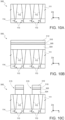
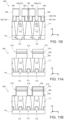
- FIGS 10A-10I show, in cross section view, steps for manufacturing the phase-change memory device 10, according to one embodiment of the present invention.
- the wafer 300 includes the substrate 114 with selector devices 113 (here, BJTs), over which the insulating layer 111 has been formed.
- the insulating layer 111 is for example is Silicon Oxide, or other insulating or dielectric material.
- a plurality of the bottom contacts, or pillars, 112 extends.
- the pillars 112 are for example formed by etching trenches in the insulating layer 111 and then filling such trenches with conductive material.
- the bottom contacts 112 extends through the insulating layer 111 for the entire thickness of the insulating layer 111.
- a step of depositing a further insulating or dielectric layer 304 on the insulating layer 111 is carried out; the insulating layer 304 is, in this embodiment, of Silicon Nitride (SiN). Then a step is carried out to form (e.g. by deposition), on the insulating layer 304, a resistive layer 305.
- the resistive layer 305 is a continuous strip or sheet of conductive material, extending on the entire surface of the insulating layer 304.
- the resistive layer 305 will form the already described resistive lamina 210.
- a further insulating layer 310 is formed by depositing, for example, the same material of the insulating layer 304. Therefore, the resistive layer 305 is actually buried between two dielectric layers.
- a masking layer 312 is formed, for example by depositing TEOS.
- the masking layer 312 is patterned to form an etching mask that is used to remove selective portions of the underlying layers, i.e. of the two dielectric layers 304, 310 and of the buried resistive layer 305.
- This etching step removes unmasked portions of such layers until respective surface regions of the insulating layer 111 are exposed.
- the mask 312 and the etching step are designed so that the remaining portions of the two dielectric layers 304, 310 and of the buried resistive layer 305 (masked stack 315) extend in a strip-like fashion along the Y axis in top-plan view (on the XY plane) and are separated from one another along the X axis by the spaces left by the removed portions.
- Each one of the masked stacks 315 extends, along the X axis, from one pillar 112 to another immediately subsequent pillar 112, only partially covering the surface of such two pillars. Two immediately subsequent pillars 112 along the X axis are partially covered by only one respective masked stacks 315.
- a step of depositing a continuous layer of resistive material 320 is carried out.
- the layer of resistive material 320 covers the masked stacks 315, the exposed surface of the pillars 112 and the exposed surface of the insulating layer 111 between the pillars 112.
- This layer of resistive material 320 will form, in subsequent steps, the plurality of heaters 102. Therefore, the material of layer 320 as well as its thickness are chosen according to the needs and/or design requirements for the heaters 102. For example, the material is TiSiN and the thickness is in the range 3.5 - 6 nm.
- an insulating layer 322 (e.g. of Silicon Nitride) is deposited to cover the masked stacks 315 and the spaces between the masked stacks 315.
- a masked etching step is then carried out to remove selective portions of the insulating layer 322 above the masked stacks 315 and between the masked stacks 315.
- the portion of the insulating layer 322 that is removed between each couple of masked stacks 315 has an extension d 1 , along the X axis, which is less than the distance d 2 , along the X axis, between such masked stacks 315.
- the etching of the insulating layer 322 is carried out for the entire thickness of the insulating layer 322, exposing respective surfaces of the underlying resistive layer 320.
- the resistive layer 320 has, during the etching of the insulating layer 322, the function of an etch-stop layer.
- a further etching step is carried out to remove the portions of the exposed resistive layer 320 through its entire thickness. This etching step can be unmasked due to the etching selectivity of the materials of the resistive layer 320 and the insulating layer 322.
- a step is then carried out to remove the mask 312 from each masked stack 315 and to remove the insulating layer 310, until the resistive layer 305 is exposed.
- This step can be carried out by means of etching chemicals that selectively remove the layers 312 and 310, or through a CMP step configured to land on the resistive layer 305 without damaging or excessively removing the resistive layer 305.
- the crystalline layer 106 is deposited; the crystalline layer 106 is of a phase-change material, in particular of a chalcogenide material, such as GST alloy.
- a sealing layer 326 e.g. of Silicon Nitride, is deposited on the crystalline layer 106 and is used as a mask for the subsequent step of Figure 10H .
- Figure 10H shows the wafer 300 in a cross section taken along the Y axis, to better appreciate the etching step that is used to define grid-like or matrix pattern of the memory cells 100.
- the crystalline layer 106 and the underlying resistive and insulating layers 305, 304 are patterned along the Y axis, to form a plurality of memory regions (identified with the same reference numeral 106) physically separated from one another and coupled each one to a respective resistive lamina 210 (layer 305) and a respective heater 102 (which is not represented in the cross section of Figure H).
- FIG. 10I shows the wafer 300 in cross section view along the XZ plane, to appreciate that each memory region 106 is coupled to one respective heater 102 and to one respective resistive lamina 210, which departs from one side only of the heater 102, leaving the other, opposite, side free from remains of the resistive layer 305.
- the manufacturing of the memory device 10 can then be completed by forming the conductive metallic layer 108 on top of the crystalline layer 106, and filling the apertures with dielectric or insulating layer(s) (not shown). Proper electrical connection can then be formed. These steps are not, per se, part of the present invention and are therefore not further discussed.
- Insulating layers 322 and 304 form the insulating layer 104 previously described.
- Figures 11A-11C show steps for manufacturing a memory device 10 wherein the selector 113 is a MOSFET device (as discussed with reference to Figure 8 ).
- a wafer 400 is provided, already processed as described with reference to Figures 10A-10B .
- the masking layer 312 is patterned to form an etching mask that is used to remove selective portions of the underlying layers, i.e. of the two dielectric layers 304, 310 and of the buried resistive layer 305. This etching step removes unmasked portions of such layers until respective surface regions of the insulating layer 111 are exposed.
- the mask 312 and the etching step are designed so that the remaining portions of the two dielectric layers 304, 310 and of the buried resistive layer 305 (masked stack 315) extend in a strip-like fashion along the Y axis in top-plan view (on the XY plane) and are separated from one another along the X axis by the spaces left by the removed portions, as in the Figure 10C .
- each one of the masked stacks 315 extends, along the X axis, from one pillar 112 (only partially covering the surface of such pillar 112) to another immediately subsequent pillar 112, fully covering the surface of such subsequent pillar 112.
- a step of depositing a continuous layer of resistive material 320 is carried out, analogously to Figure 10D .
- This layer forms, in further steps, the heater 102.
- the manufacturing of the memory device 10 can then be completed by forming the conductive metallic layer 108 on top of the crystalline layer 106, and filling the apertures with dielectric or insulating layer(s) (i.e., completing the formation of insulating layer 104). Proper electrical connection can then be formed. These steps are not, per se, part of the present invention and are therefore not further discussed.
- Figures 12A-12H show steps for manufacturing the memory device of Figure 6 , where the resistive lamina 210 extends from the heater 102 as an integral part of the heater 102.
- a wafer 500 is provided, which has already been subject to manufacturing steps known in the art and therefore not further detailed.
- the wafer 500 has been processed to form, in the substrate 114, the selectors 113 (here, BJT selector devices 113); over the substrate 114, the insulating layer 111 has been formed.
- the insulating layer 111 is for example is Silicon Oxide, or other insulating or dielectric material.
- 112 of conductive material such as metal or doped polysilicon
- the bottom contacts 112 extends through the insulating layer 111 for the entire thickness of the insulating layer 111.
- a step of depositing a further insulating or dielectric layer 504 on the insulating layer 111 is carried out; the insulating layer 504 is, in this embodiment, of Silicon Nitride (SiN).
- the insulating layer 111 is patterned (e.g. by photolitographic and etching processes).
- the etching step removes unmasked portions of the insulating layer 504 until respective surface regions of the insulating layer 111 are exposed.
- the patterning is designed so that the remaining portions of the dielectric layer 504 extend in a strip-like fashion along the Y axis in top-plan view (on the XY plane) and are separated from one another along the X axis by the spaces left by the removed portions.
- Each one of the remaining portions of the dielectric layer 504 extends, along the X axis, from one pillar 112 to another immediately subsequent pillar 112, only partially covering the surface of such two pillars.
- Two immediately subsequent pillars 112 along the X axis are partially covered by only one respective remaining portion of the dielectric layer 504.
- a step of depositing a continuous layer of resistive material 520 is carried out.
- the layer of resistive material 520 covers the portions of the dielectric layer 504, the exposed surface of the pillars 112 and the exposed surface of the insulating layer 111 between the pillars 112.
- This layer of resistive material 520 will form, in subsequent steps, the plurality of heaters 102 as well as the resistive laminas 210. Therefore, the material of layer 520 as well as its thickness are chosen according to the needs and/or design requirements for the heaters 102 and of the resistive laminas 210.
- the material is TiSiN and the thickness is in the range 3.5 - 6 nm.
- a protection layer 522 e.g. of Silicon Nitride
- a filling layer 525 is carried out, filling the gaps between the portions of the dielectric layer 504 and covering the portions of the dielectric layer 504.
- a step is then carried out, Figure 12E , to remove selective portions of the filling layer 525 above the portions of the dielectric layer 504, exposing the resistive layer 520 resting on top of such portions of the dielectric layer 504.
- the filling layer 525 remains between such portions of the dielectric layer 504.
- This step can be carried out by means of a masked etching process (e.g., a lithographic process), or through a CMP step configured to land on the resistive layer 520 without damaging or excessively removing the resistive layer 520 on top of the portions of the dielectric layer 504.
- the crystalline layer 106 is deposited; the crystalline layer 106 is of a phase-change material, in particular of a chalcogenide material, such as GST alloy.
- a sealing layer 526 e.g. of Silicon Nitride, is deposited on the crystalline layer 106 and is used as a mask for the subsequent step of Figure 12G .
- Figure 12G shows the wafer 500 in a cross section taken along the Y axis, to better appreciate the etching step that is used to define grid-like or matrix pattern of the memory cells 100.
- the crystalline layer 106 and the underlying resistive and insulating layers 320, 504 are patterned along the Y axis, to form a plurality of memory regions (identified with the same reference numeral 106) physically separated from one another and coupled each one to a respective heater 102.
- FIG 12H shows the wafer 500 along the X axis, to appreciate that each memory region 106 is coupled to one respective heater 102 and to one respective resistive lamina 210, which departs from one side only of the heater 102 and is integral with the heater 102, leaving the other, opposite, side free from remains of the resistive layer 520 running along the X axis.
- Layers 504, 522 and 525 will form, as a whole, the insulating layer 104 already mentioned.
- the manufacturing of the memory device 10 can then be completed by forming the conductive metallic layer 108 on top of the crystalline layer 106, and filling the apertures with dielectric or insulating layer(s), thus completing the formation of the insulating layer 104. Proper electrical connection can then be formed. These steps are not, per se, part of the present invention and are therefore not further discussed.
- Figures 13A-13C show steps for manufacturing a memory device 10 where the resistive lamina 210 extends from the heater 102 as an integral part of the heater 102, but the selector devices 113 are MOSFET.
- a wafer 550 is provided, which has already been subject to manufacturing steps known in the art and therefore not further detailed.
- the wafer 550 includes the substrate 114, over which the insulating layer 111 extends.
- the insulating layer 111 is for example is Silicon Oxide, or other insulating or dielectric material.
- Through the insulating layer 111 a plurality of the bottom contacts, or pillars, 112 (of conductive material such as metal or doped polysilicon) extends.
- the bottom contacts 112 extends through the insulating layer 111 for the entire thickness of the insulating layer 111.
- a step of depositing a further insulating or dielectric layer 554 on the insulating layer 111 is carried out; the insulating layer 554 is, in this embodiment, of Silicon Nitride (SiN).
- the insulating layer 554 is patterned (e.g. by photolitographic and etching processes).
- the etching step removes selective portions of the insulating layer 554 until respective surface regions of the insulating layer 111 are exposed.
- the patterning is designed so that the remaining portions of the dielectric layer 554 extend in a strip-like fashion along the Y axis in top-plan view (on the XY plane) and are separated from one another along the X axis by the spaces left by the removed portions.
- Each one of the remaining portions of the dielectric layer 554 extends, along the X axis, from one pillar 112 (only partially covering the surface of such pillar 112) to another immediately subsequent pillar 112, fully covering the surface of such subsequent pillar 112.
- a step of depositing a continuous layer of resistive material 560 is carried out.
- the layer of resistive material 560 covers the portions of the dielectric layer 554, the exposed surface of the pillars 112 and the exposed surface of the insulating layer 111 between the pillars 112.
- This layer of resistive material 560 will form, in subsequent steps, the plurality of heaters 102 as well as the resistive laminas 210. Therefore, the material of layer 560 as well as its thickness are chosen according to the needs and/or design requirements for the heaters 102 and of the resistive laminas 210.
- the material is TiSiN and the thickness is in the range 350-400 nm.
- the manufacturing of the memory device 10 can then be completed by forming the conductive metallic layer 108 on top of the crystalline layer 106, and filling the apertures with dielectric or insulating layer(s). Proper electrical connection can then be formed. These steps are not, per se, part of the present invention and are therefore not further discussed.
- FIG 14 schematically shows an embodiment of a memory 600.
- the memory 600 comprises: one or a plurality of memory devices, such as devices comprising memory cells 100 previously described in relation to each of the embodiments disclosed, and shown in Figure 14 by a block 602 (NVM) ; a data processing unit, represented by a block 604 (PU), for example, a microprocessor; one or a plurality of memory devices, represented by a block 606 (MEM), and which may be memory devices different from those of block 602; a block 608 (FCT) comprising other electronic functions, for example, sensors, load control circuits, etc.; and a data bus 610 enabling to transfer data between the different components.
- the block 602 preferably includes a circuit for addressing the array of memory cells 100.
- the memory devices of the block 506 not to be phase-change memory devices but to be RAMs, reprogrammable volatile memories (EEPROM, flash, etc.).
- the block 606 may be omitted.
- the memory devices of the memory 600 are then only memory devices such as memory devices comprising memory cells 100.
- the memory is then entirely a non-volatile memory.
Landscapes
- Engineering & Computer Science (AREA)
- Manufacturing & Machinery (AREA)
- Chemical & Material Sciences (AREA)
- Crystallography & Structural Chemistry (AREA)
- Semiconductor Memories (AREA)
- Chemical Vapour Deposition (AREA)
Abstract
Description
- The present disclosure relates generally to a phase-change memory cell, a memory device including the phase-change memory cell, and a method for manufacturing the phase-change memory cell. The phase-change memory cell is, in particular, for multibit storage.
- Phase-change materials are materials which can switch, under the effect of heat, between a crystalline phase and an amorphous phase, or between different detectable states of local order across the entire spectrum between completely amorphous and completely crystalline states. Since the electric resistance of an amorphous material is significantly greater than the electric resistance of a crystalline phase of the same material, such a phenomenon is used to define two memory states, for example, 0 and 1, differentiated by the resistance measured through the phase-change material.
- As is known, phase change memory devices use phase change materials for electronic memory application. The state of the phase change materials is also non-volatile in that, when set in either a crystalline, semi-crystalline, amorphous, or semi-amorphous state representing a resistance value, that value is retained until changed by another programming event, as that value represents a phase or physical state of the material (e.g., crystalline or amorphous). The state is unaffected by removing electrical power.
- At present, alloys of group VI of the periodic table, such as Te or Se, referred to as chalcogenides or chalcogenide materials, can advantageously be used in phase change cells as phase change materials. The most promising chalcogenide is formed by a Ge, Sb and Te alloy (Ge2 Sb2 Te5 ), also called GST, which is currently widely used for storing information in overwritable disks.
- In chalcogenides, the resistivity varies by two or more magnitude orders when the material passes from the amorphous phase (more resistive) to the crystalline phase (more conductive) and vice versa.
- Phase change may be obtained by locally increasing the temperature. Below 150°C all phases are stable. Above 200°C (temperature of start of nucleation), fast nucleation of the crystallites takes place, and, if the material is kept at the crystallization temperature for a sufficient length of time, it changes its phase and becomes crystalline (so-called set state) . To bring the chalcogenide back into the amorphous state (reset state), it is necessary to raise the temperature above the melting temperature (approximately 600°C) and then to cool the chalcogenide off rapidly. Intermediate phases may be obtained applying suitable temperatures for different times, which cause the formation of amorphous "spots" or "bubbles" of different dimensions in contact with the heater.
- From the electrical standpoint, it is possible to cause the chalcogenide material to change state by causing a current to flow through a resistive element, called a heater, which heats the chalcogenide material by the Joule effect.
- The basic structure of a
PCM element 1 which operates according to the principles described above is shown inFigure 1 and comprises aheater element 2 and amemory element 3 of chalcogenide material. A portion of the memory element 3 (generally crystalline or polycrystalline) is in thermal contact with theheater 2 and is subject to phase change between amorphous and crystalline (i.e., thememory element 3 can assume a crystalline state, or an amorphous state, or even one or more intermediate states between the crystalline and the amorphous states).Figure 1 shows a PCM element in an intermediate state, wherein the portion that has not changed phase and enables a good flow of current is referred to ascrystalline portion 4 and the portion that has changed state is referred to asamorphous portion 5. The dimensions of theamorphous portion 5 define the overall resistivity of thememory region 3 and thus of thePCM element 1. Thus, different resistance levels may be associated with different bits and may be obtained by generating appropriate program currents that cause theamorphous portion 5 to assume different dimensions. - A conductive layer 7 (having a predefined electrical resistance, and therefore also named in the following "resistive layer") is interposed between the
memory element 3 and theheater 2, as well as between thememory element 3 and an insulating, or dielectric,layer 6, which laterally surrounds theheater 2. In other words theresistive layer 7 is formed and rests both on the upper surface of thedielectric layer 6 and on the upper surface of theheater 2, theresistive layer 7 being in electrical contact with theheater 2. Thememory element 3 is formed and rests on the upper surface of theresistive layer 7. Theresistive layer 7 is for example made of any refractory metal and/or refractory metal nitride, such as TiN (titanium nitride), Ta (tantalum), TaN (tantalum nitride), or W (tungsten). - Reference is also made to
Figures 2A-2D , showing thePCM element 1 ofFigure 1 in different programming conditions, obtained using progressively higher programming currents. InFigures 2A-2D , the same reference numbers have been used as inFigure 1 , whilenumber 6 represents the layer of insulating or dielectric material that surrounds theheater 2. - As visible in
Figures 2A-2D , theamorphous portions 5 have different dimensions (radiuses). In detail, inFigure 2A , where a lower programming current ip was used (e.g., ip = 160-200 µA), thephase change portion 5 extends just a little beyond the edge of theheater 2, while inFigures 2B, 2C, 2D (obtained with progressively higher programming currents ip - up to 300-350 µA) the protruding portion of thephase change portion 5 is gradually bigger. - The current path from the
heater 2 to thecrystalline portion 4 is influenced by the high resistiveamorphous portion 5; therefore the current path resistance is very high in all four conditions. Thus, the difference in resistance among the four conditions is small, compared with its absolute value. - Moreover, the programmed resistance is entirely associated to the high resistivity of the amorphized portion.
- Patent
EP2034536B1 discusses a multilevel architecture for PCM. Resistance of intermediate states between two programming states (also known as SET and RESET) is (geometrically) controlled by the volume of theamorphous portion 5. - During reading, the electrical current flows through two parallel paths (not shown) so as to circumvent the
amorphous portion 5. That is to say that a read current flows in theresistive layer 7 instead of theamorphous portion 5. Each one of these two paths includes one respective of the two branches of theresistive layer 7 that extend in an opposite direction from the upper surface of theheater 2, and are covered by the amorphous portion 5 (each branch having a resistance RL). The amorphous volume ofportion 5 only determines the length of theresistive layer 7 through which the reading current flows (and so the electrical resistance seen by the current) for a certain programmed state SET / RESET. - Benefits of this approach include that temperature dependence, drift and 1/f noise are drastically mitigated. However, a gap between the resistance values of the two states SET / RESET is reduced by the fact that, for every amorphous volume configuration, there exist two identical current paths in parallel (due to the symmetry of the layout of the resistive layer 7). For example, by defining: the resistance in the SET state as RSET=RH; the resistance in the RESET state as RRESET=RH+RL/2 (where RL/2 is the equivalent resistance of the portion of the
resistive layer 7 through which the current flows during reading of thememory element 3 when programmed in the RESET state). - The ratio between RRESET and RSET represents the window W, or the gap, between the resistance values of the two states SET / RESET:

- The higher the window W, the easier the detection of the respective state SET/RESET during reading.
-
- Document
US2021/135104 generally relates to phase change memory devices, and more particularly to phase change memory devices having a phase change region with a mushroom shape. - However, the above-mentioned issues are not solved.
- The aim of the invention is thus to provide a phase-change memory cell, a memory device including the phase-change memory cell, and a method for manufacturing the phase-change memory cell, having an improved behavior and overcoming the above-mentioned drawbacks.
- According to the present invention, there are provided a phase-change memory cell, a memory device including the phase-change memory cell, and a method for manufacturing the phase-change memory cell, as defined respectively in the annexed claims.
- The foregoing features and advantages, as well as others, will be described in detail in the following description of specific embodiments given by way of illustration and not limitation with reference to the accompanying drawings, in which:
For a better understanding of the present invention, preferred embodiments thereof are now described, purely by way of non-limiting example and with reference to the attached drawings, wherein: -
Figure 1 shows an exemplary structure of a known phase change memory element; -
Figures 2A-2D show the phase change memory element ofFigure 1 in different programming conditions; -
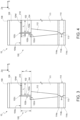
Figure 3 is a simplified cross-section view of an example of a phase-change memory device including a phase-change memory cell according to an embodiment of the present invention; -
Figure 4 is a simplified cross-section view of an example of a phase-change memory device including a phase-change memory cell according to a further embodiment of the present invention; -
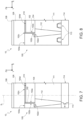
Figure 5 is a simplified cross-section view of an example of a phase-change memory device including a phase-change memory cell according to a further embodiment of the present invention; -
Figure 6 is a simplified cross-section view of an example of a phase-change memory device including a phase-change memory cell according to a further embodiment of the present invention; -
Figure 7 is a simplified cross-section view of an example of a phase-change memory device including a phase-change memory cell according to a further embodiment of the present invention; -
Figure 8 is a simplified cross-section view of an example of a phase-change memory device including a phase-change memory cell according to a further embodiment of the present invention; -
Figures 9A-9C show three simplified cross-sections views of various steps of a method of writing into the phase-change memory cell ofFigure 3 , or ofFigures 4-8 ; -
Figures 10A-10I show process steps carried out on a wafer for manufacturing the phase-change memory device ofFigure 3 ; -
Figures 11A-11C show process steps carried out on a wafer for manufacturing the phase-change memory device ofFigure 8 ; -
Figures 12A-12H show process steps carried out on a wafer for manufacturing the phase-change memory device ofFigure 5 ; -
Figures 13A-13C show process steps carried out on a wafer for manufacturing a further phase-change memory device not shown in the previous figures; and -
Figure 14 schematically shows an embodiment of a memory. - Like features are designated by like references in the various figures. In particular, the structural and/or functional features that are common among the various embodiments may have the same references and may dispose identical structural, dimensional and material properties.
- For the sake of clarity, only the operations and elements that are useful for an understanding of the embodiments described herein have been illustrated and described in detail. In particular, the memory cells comprise elements which are not detailed, such as selection elements (transistors, for example) or electric connections.
-
Figure 3 is a simplified perspective view of amemory cell 100, which is part of a phase-change memory (PCM) device 10 (only a portion of which is represented), the phase-change memory device 10 comprising a plurality ofmemory cells 100.Figure 3 show thememory cell 100 in a triaxial system of mutually orthogonal axes X, Y, Z (Cartesian system). - Phase-change memory cells, such as
memory cells 100 depicted inFigure 3 , are typically embedded in non-volatile memory (NVM) devices such as electrically erasable programmable read-only memories (EEPROM). The programming of each memory cell in such memory devices is usually performed upon manufacturing of the memory devices and can afterwards be modified several times, particularly during their use. - The
memory cells 100 of thememory device 10 are arranged in a grid-like or matrix pattern. In other words, thememory device 10 is composed of an array ofmemory cells 100. Eachmemory cell 100 is located at the intersection of a row and a column of the array. - The columns, which are parallel to each other, are also referred to as "bit lines" (BL). The rows, which are parallel to each other and perpendicular to the bit lines, are also referred to as "word lines" (WL).
- Each phase-
change memory cell 100 of thememory device 10 comprises aheater 102 or resistive element. In the example ofFigure 3 , theheater 102 has an L-shaped cross-section (therefore having a vertical portion extending along the Z axis and a horizontal portion extending along the X axis). However, other shapes are possible, such as a "I" shaped cross-section (where only the vertical portion is present). - The
heater 102 is generally surrounded by one or more insulating or dielectric layers (only onelayer 104 is represented inFigure 3 ), typically composed of nitrate (e.g. SiN) and/or oxide (e.g. SiO2). - The
upper surface 102c of the vertical portion of theheater 102 is coplanar with theupper surface 104a of the insulatinglayer 104. As better explained later, the thickness t1 along Z axis of this insulatinglayer 104 is such that, at oneside 102a of theheater 102, is less than the thickness t2 of the insulatinglayer 104 at theopposite side 102b (along X axis) of theheater 102. The thickness t1 is reduced with respect to thickness t2 due to the presence of an electricallyconductive layer 210 having a resistive characteristic (in the following, also referred to as "resistive lamina 210"). Theresistive lamina 210 has a main extensions along the X, and extends (or protrudes) fromside 102a of theheater 102 away from theheater 102. Theupper surface 104a' of the insulatinglayer 104 extending at theside 102a of theheater 102 is coplanar with the lower surface of theresistive lamina 210. - Each
memory cell 100 further comprises anown memory region 106, which is separated fromother memory regions 106 by an interposed dielectric or insulating layer. Thismemory region 106 is made of a phase-change material. Thememory region 106 is for example made of a chalcogenide material such as an alloy that belongs at the Tellurium-based chalcogenide alloys family, in particular an alloy including germanium (Ge), antimony (Sb) and tellurium (Te). Such alloy is known as "GST". There are others chalcogenide alloys families (selenium-based and sulfur-based) that can be used for manufacturing thememory region 106. In any case, the present invention is not limited to a specific material of thememory region 106. - The
memory region 106 is configured to switch between a crystalline phase (or state) and an amorphous phase (or state), and can be permanently set in one of such phases (or states). Therefore, during use thememory region 106 can be set in a crystalline state, or an amorphous state, or even one or more intermediate states between the crystalline state and the amorphous state. - Typically, a crystalline phase of the
memory region 106 is native (that is to say after manufacturing/fabricating thememory cell 100 and before the beginning of writing/programming operations,memory region 106 is in a wholly crystalline state/phase). Accordingly, in the following description, thememory region 106 can also be referred to as "crystalline layer 106". - The
crystalline layer 106 is formed and rests both on theupper surface 104a of the insulatinglayer 104 and on theupper surface 102c of the vertical portion of theheater 102. Theheater 102 is in electrical and thermal contact with thecrystalline layer 106 through the vertical portion of theheater 102. - The
heater 102 is, in the embodiment shown inFigure 3 , centered with respect to an axis of symmetry (parallel to the Z axis and orthogonal to the X axis) of thememory cell 100. - According to an aspect of the present invention, the
resistive lamina 210, already mentioned, is interposed between a portion of the insulatinglayer 104 and a respective portion of thecrystalline layer 106, laterally to theheater 102. Theheater 102 is in electrical contact with theresistive lamina 210, in particular in direct electrical contact with theresistive lamina 210. In particular, theresistive lamina 210 is laterally connected to the heater 102 (i.e., it is connected to theheater 102 at theside 102a of the heater 102). - The
resistive lamina 210 has an own upper surface that is coplanar with theupper surface 102c of the heater 102 (on plane XY in the drawings). In other words, the upper surface of theresistive lamina 210 extends as a continuation of theupper surface 102c of theheater 102 and lies on the same plane XY as theupper surface 102c. - A conductive
metallic layer 108 extends on top of thecrystalline layer 106. Thisconductive layer 108 typically forms an electrode of thememory cell 100. Conductive vias (not shown) may be provided for connecting eachelectrode 108, e.g. to a metallization level located above thememory cells 100 of thememory device 10. - The
conductive layer 108 forms an electrode (to be connected to the bit line) of thememory cell 100, while theheater 102 forms another electrode (to be connected to the word line) of thememory cell 100. The two electrodes are also referred to here as a "top"electrode 108 and a "bottom"electrode 102, though no limitation is implied as tomemory cell 100 orientation in operation. - The
heater 102 of thememory cell 100 is typically connected, by itsfoot 102d (that is to say a bottom surface of its horizontal portion), to a bottom contact, or pillar, 112, which is of conductive material such as doped polysilicon or metal. Thisbottom contact 112 extends vertically through an insulatinglayer 111 and is connected to asubstrate 114 that extends below the insulatinglayer 111. - The
substrate 114 can have a multilayer structure, for example composed of three layers: afirst layer 114a made of a thin silicon film, to which thebottom contacts 112 are connected; asecond layer 114b made of a thin buried oxide; and athird layer 114c composed of a material suitable for providing mechanical support, also called "handle substrate". - The
bottom contact 112 of eachmemory cell 100 is connected to one terminal of aselection element 113. Theselection element 113, often termed selector or access device, provides the ability to address/select individually eachmemory cell 100 of thememory device 10. - In the example of
Figure 3 , theselector 113 is a BJT device, with an emitter terminal electrically coupled to thebottom contact 112, a collector terminal electrically coupled to a common reference potential, typically a ground potential, and a base terminal that, in use, receives a bias voltage. - The crystalline phase of the
memory region 106 corresponds, for example, to the logic value "1". Data storage inside the phase-change memory 10 is then carried out by writing/programming some of itsmemory cells 100, while other of itsmemory cells 100 are left in their native state (that is to say in a crystalline state). - For writing, or programming, into a given phase-
change memory cell 100 ofmemory 10, thismemory cell 100 is first selected by applying an appropriate voltage bias to the base terminal of the BJT. An electrical current then flows through thecrystalline layer 106. The electrical potential or the intensity of this electric current is tuned so as to sufficiently increase the temperature of theheater 102 to heat, by Joule heating, an area of thecrystalline layer 106 in contact with theupper end 102c of theheater 102. This causes at least part of the phase-change material to melt. When the potential pulse is abrupt, the electric current flow rapidly ends and, consequently, the local temperature of the phase-change material rapidly decreases, quenching the glassy structure of the melted part of the phase-change material. As a result, the electrical pulse has transformed a part of the phase-change material from a low resistive crystalline phase to a highly resistive amorphous state. It is assumed, for example, that this amorphous state corresponds to the logic value "0". - For reading a given phase-
change memory cell 100, thismemory cell 100 is first selected by applying an appropriate voltage bias to the base terminal of the BJT. A current, whose value is low enough to avoid any inadvertent phase change, is then flown through thecell 100 by applying an appropriate electrical potential by activating the selector element. An electrical resistance, between theelectrode 108 and theheater 102, can then be measured. This electrical resistance reflects the value "0" or "1" that was previously stored in thememory cell 100. - The material of
resistive lamina 210 may be selected as a trade-off between programming current and an ability to discern intermediate programming states represented by different resistance levels. The electrical resistance of theresistive lamina 210 is chosen according to the needs, for example about the value of the electrical resistance of theheater 210, and / or less than the electrical resistance of the amorphous region of thelayer 106. More particularly, the resistivity value oflamina 210 is between the respective resistivity values of the crystalline and amorphous states of the phase change material of thecrystalline layer 106. The resistivity of thelamina 210 can be significantly lower than the resistivity of the amorphous state of the phase change material. For example, resistivity oflamina 210 can be between about 1/1000 times and 1/10 times the resistivity of the amorphous state of the phase change material oflayer 106. At the same time, the resistivity of thelamina 210 is higher than the resistivity of the crystalline state of the phase change material. In an embodiment,lamina 210 may be selected to have a resistivity in the range of about 1mΩ·cm - 0.1Ω·cm. Example materials that may be utilized forlamina 210 may include, but are not limited to, carbon (C) and metallic compounds such as TiSiN, TiAlN, and SiC. Other materials traditionally used for resistors in the integrated circuit industry can also be employed. For example, theresistive lamina 210 can also be made of any refractory metal and/or refractory metal nitride, such as TiN (titanium nitride), Ta (tantalum), TaN (tantalum nitride), or W (tungsten). - The
resistive lamina 210 has a thickness, along the Z axis, lower than 10 nm, preferably comprised between 1 and 10 nm, most preferably of 4-5 nm. - According to the present invention, the
resistive lamina 210 has an extension t3, along the X axis in the cross section view ofFigure 3 , which is greater at one side of theheater 102 with respect to the opposite side of theheater 102. - In particular, in the embodiment of
Figure 3 , theresistive lamina 210 extends only at theside 102a of the heater 102 (the right-hand side in theFigure 3 ), in electrical contact with theheater 102 at theside 102a (in particular, in direct electrical contact). At theopposite side 102b of the heater 102 (the left-hand side in theFigure 3 ), theresistive lamina 210 is absent. - According to a further embodiment, illustrated in
Figure 4 , theresistive lamina 210 also extends at thesecond side 102b of theheater 102, and is in electrical contact with theheater 102 at bothsides resistive lamina 210 at thesecond side 102b of theheater 102 is less than the length t3 (along X axis) of the portion of theresistive lamina 210 at thefirst side 102a of theheater 102. In particular, the length t3 corresponds, along the X axis and at theside 102a of theheater 102, to the whole length of thecrystalline layer 106 extending at theside 102a (i.e. the length of thelayer 106 measured along X axis starting fromside 102a until the end of thelayer 106 of thememory cell 100 considered). The length t4 corresponds, along the X axis and at theside 102b of theheater 102, to a fraction of the length of thecrystalline layer 106 extending at theside 102b (i.e. the length of thelayer 106 measured along X axis starting fromside 102b until the end of thelayer 106 of thememory cell 100 considered). - In a further embodiment, shown in
Figure 5 , theresistive lamina 210 is integral with theheater 102 and extends with continuity from theheater 102, in particular fromside 102a of theheater 102. Therefore, in this embodiment, theresistive lamina 210 is of the same material of theheater 102 and is formed during the same step of forming theheater 102. - As discussed with reference to
Figure 3 and Figure 4 , also in the embodiment ofFigure 5 theresistive lamina 210 has an extension t3, along the X axis in the cross section view ofFigure 4 , which is greater on one side (here,side 102a) of theheater 102 with respect to the opposite side (here,side 102b) of theheater 102. In particular, in the embodiment ofFigure 5 , theresistive lamina 210 is present only at theside 102a and is absent at theside 102b. - In the embodiment of
Figure 6 , which is based on the embodiment ofFigure 5 , theresistive lamina 210 is integral with theheater 102 and also extends at theside 102b of theheater 102. The length t4 of the portion of theresistive lamina 210 at theside 102b is less than the length t3 (along X axis) of the portion of theresistive lamina 210 at thefirst side 102a. - As shown in
Figure 7 , according to a further embodiment of the present invention, the heater 102 (in particular the vertical portion of the heater 102) is not centered with respect to the axis of symmetry of the memory cell 100 (represented inFigure 7 and identified as SZ), but staggered, or offset, with respect to such axis of symmetry; in other words, theheater 102 and thepillar 112 are shifted either to the left-hand side or to the right-hand side with respect to the axis of symmetry SZ. Even thoughFigure 7 shows the case where theresistive lamina 210 is not integral with the heater 102 (embodiments ofFigures 3 and 4 ), the teaching ofFigure 7 applies to the embodiment in which theresistive lamina 210 is integral with the heater 102 (as inFigures 5 and 6 ). - Furthermore, also in the embodiment of
Figure 7 theresistive lamina 210 has an extension, along the X axis in cross section view, which is greater onside 102a of theheater 102 with respect to theopposite side 102b of theheater 102. In particular, theresistive lamina 210 may be present only at theside 102a and be absent at thesecond side 102b; or theresistive lamina 210 also extends at thesecond side 102b of theheater 102, wherein the length of the portion of theresistive lamina 210 at thesecond side 102b is less than the length (along X axis) of the portion of theresistive lamina 210 at thefirst side 102a. - As shown in
Figure 8 , according to a further embodiment of the present invention, theselector 113 is a MOSFET device, having one conduction terminal (source or drain) electrically coupled to thebottom contact 112, the opposite conduction terminal (drain or source) electrically coupled to a common reference potential, typically a ground potential, and the gate that, in use, receives a bias voltage. According to its value, this bias voltage allows to enable or disable a current flow through the selector. In the example ofFigure 8 , the select transistors ofmemory cells 100 belonging to a given word line or row share the same gate. In the memory device, the gates extend longitudinally along the WL direction (to the front and to the back, inFigure 8 ). All the select transistors of memory cells of a given word line are consequently connected to a same gate. Both theconductive layers 108 and the gates hence form a matrix or grid-like pattern, in which each intersection is roughly vertically aligned with amemory cell 100. - When MOSFET devices are used as selector devices, dummy heaters (not shown) may be implemented to account for dimensions and electrical connections of the gates.
-
Figure 8 is based onFigure 3 ; however, a MOSFET asselector device 113 can be implemented to the embodiments ofFigures 4-7 as well. -
Figures 3-8 show respective embodiments where theresistive lamina 210 has a greater length (along the X axis) at the right-hand side 102a of theheater 102 with respect to the left-hand side 102b (where thelamina 210 can even be absent). However, the teaching of the present description applies analogously to embodiments (not shown) where theresistive lamina 210 extends only from the left-hand side 102b of theheater 102, or has a greater length (along the X axis) from the left-hand side 102b of theheater 102 with respect to the right-hand side 102a. Analogously, amemory device 10 may comprise a plurality ofmemory cells 100, wherein one or more (but not all) ofsuch memory cells 100 include one respectiveresistive lamina 210 extending only from the right-hand side 102a of therespective heater 102, or have a greater length (along the X axis) from the right-hand side 102a of theheater 102 with respect to the left-hand side 102b; the remaining one ormore memory cells 100 ofsuch memory device 10 extend only from the left-hand side 102b of theheater 102, or have a greater length (along the X axis) from the left-hand side 102b of theheater 102 with respect to the right-hand side 102a. See for exampleFigure 10I , where a portion of adevice 10 is shown, including someheaters 102 with a respectiveresistive lamina 210 extending from the right-hand side 102a andother heaters 102 with a respectiveresistive lamina 210 extending from the left-hand side 102b of theheater 102. - Writing operations are discussed with reference to
Figure 9A-9C , where only a portion of the phase-change memory 10 ofFigure 3 is shown (in particular, a detail of the phase-change cell 100). For writing in thememory cell 100, a voltage is applied between the top electrode 108 (conductive layer) and the bottom electrode, orheater 102. This voltage gives rise to an electric current flowing through thelayer 106, which is initially wholly made of the crystalline phase. Thememory cell 100 is thus heated, by theheater 102, up to a temperature sufficient to amorphize at leastpart 105a of thecrystalline layer 106. - In the view of
Figure 9B , Joule heating due to the electric current flowing through thememory cell 100 makes abigger part 105b of thelayer 106 change phase, thereby forming a greater amorphous region above theupper surface 102c of theheater 102. The amorphous region forms a dome which is vertically aligned with theupper surface 102c of the vertical portion of theheater 102. - In the view of
Figure 9C , increased heating, obtained with proper increased electric current flowing through thememory cell 100, makes a still bigger part 105c of thelayer 106 change phase, thereby forming a still greater amorphous region above theupper surface 102c of theheater 102. The process during which crystalline GST is turned into amorphous GST can lead to a situation where the upper surface of theresistive lamina 210 is fully covered by amorphous GST. - In the amorphous region located directly above the
heater 102, the GST of which thelayer 106 is made of has changed/switched phase, due to heating, from a crystalline phase to an amorphous state. The layout of theresistive lamina 210, which in this example extends only at one side of theheater 102, has no impact on the formation of theamorphous regions 105a-105c. The shape and location of the amorphous region is, in fact, a function of the arrangement of theheater 102. If a memory cell, like thememory cell 100 as depicted inFigures 9A-9C , is selected for reading and if the appropriate voltage bias is applied between thetop electrode 108 and the bottom electrode (or heater 102), the electrical reading current flows through thelayer 106, to reach theresistive lamina 210 present at one side of theheater 102. - The
memory cell 100 enables multilevel programming, as shown inFigures 9A-9C . In this case, it is assumed that the voltage, applied between thetop electrode 108 and the bottom electrode during the writing (programming) operation, is raised in order to increase the intensity of the electric current flowing through thelayer 106. This results in a temperature rise inside thelayer 106, thus causing the phase change to carry on within the crystalline phase around the already amorphized region. More and more of the crystalline GST, contained inside the crystalline region, is therefore progressively converted into amorphous GST which results in a progressively extended amorphous region as the programming current progressively increases. - Consistently, the extent of the part of the
resistive lamina 210 covered by the amorphous region also enlarges (as shown progressively inFigures 9A-9C ) and its resistance increases, roughly proportionally to a length of the surface of thelamina 210 that is covered by the amorphous region. Therefore, the reading resistance of thecell 100 also increases. - With the above-described embodiments of the present invention, the
resistive lamina 210 is asymmetric at least along one axis (here, the X axis). In particular, introducing an asymmetry with theresistive lamina 210 forces the reading current to flow only in a specific direction, namely where theresistive lamina 210 is present. With this solution, the window W, or gap, between the resistance values of two states SET / RESET (as well as intermediate programmed states as in a multi-states memory for multibit storage) is increased with respect to the known solutions. In particular, if the resistance in the SET state is RSET=RH, the resistance in the RESET state is RRESET=RH+RL (where RL is the resistance of the portion of theresistive lamina 210 through which the current flows during reading). - The ratio between RRESET and RSET that defines the window W is:

factor 2 with respect to the solution of the known art. -
Figures 10A-10I show, in cross section view, steps for manufacturing the phase-change memory device 10, according to one embodiment of the present invention. - With reference to
Figure 10A , awafer 300 is provided, which has already been subject to manufacturing steps known in the art and therefore not further detailed. In particular, thewafer 300 includes thesubstrate 114 with selector devices 113 (here, BJTs), over which the insulatinglayer 111 has been formed. The insulatinglayer 111 is for example is Silicon Oxide, or other insulating or dielectric material. Through the insulating layer 111 a plurality of the bottom contacts, or pillars, 112 (of conductive material such as metal or doped polysilicon) extends. Thepillars 112 are for example formed by etching trenches in the insulatinglayer 111 and then filling such trenches with conductive material. Thebottom contacts 112 extends through the insulatinglayer 111 for the entire thickness of the insulatinglayer 111. - With reference to
Figure 10B , a step of depositing a further insulating ordielectric layer 304 on the insulatinglayer 111 is carried out; the insulatinglayer 304 is, in this embodiment, of Silicon Nitride (SiN). Then a step is carried out to form (e.g. by deposition), on the insulatinglayer 304, aresistive layer 305. Here, at this step of process, theresistive layer 305 is a continuous strip or sheet of conductive material, extending on the entire surface of the insulatinglayer 304. In further steps of manufacturing, described later, theresistive layer 305 will form the already describedresistive lamina 210. On theresistive layer 305, a further insulatinglayer 310 is formed by depositing, for example, the same material of the insulatinglayer 304. Therefore, theresistive layer 305 is actually buried between two dielectric layers. On the insulatinglayer 310, amasking layer 312 is formed, for example by depositing TEOS. - Then,
Figure 10C , themasking layer 312 is patterned to form an etching mask that is used to remove selective portions of the underlying layers, i.e. of the twodielectric layers resistive layer 305. This etching step removes unmasked portions of such layers until respective surface regions of the insulatinglayer 111 are exposed. In detail, themask 312 and the etching step are designed so that the remaining portions of the twodielectric layers masked stacks 315 extends, along the X axis, from onepillar 112 to another immediatelysubsequent pillar 112, only partially covering the surface of such two pillars. Two immediatelysubsequent pillars 112 along the X axis are partially covered by only one respectivemasked stacks 315. - A shown in
Figure 10D , a step of depositing a continuous layer ofresistive material 320 is carried out. The layer ofresistive material 320 covers themasked stacks 315, the exposed surface of thepillars 112 and the exposed surface of the insulatinglayer 111 between thepillars 112. This layer ofresistive material 320 will form, in subsequent steps, the plurality ofheaters 102. Therefore, the material oflayer 320 as well as its thickness are chosen according to the needs and/or design requirements for theheaters 102. For example, the material is TiSiN and the thickness is in the range 3.5 - 6 nm. - Then,
Figure 10E , an insulating layer 322 (e.g. of Silicon Nitride) is deposited to cover themasked stacks 315 and the spaces between the masked stacks 315. A masked etching step is then carried out to remove selective portions of the insulatinglayer 322 above themasked stacks 315 and between the masked stacks 315. The portion of the insulatinglayer 322 that is removed between each couple ofmasked stacks 315 has an extension d1, along the X axis, which is less than the distance d2, along the X axis, between suchmasked stacks 315. The etching of the insulatinglayer 322 is carried out for the entire thickness of the insulatinglayer 322, exposing respective surfaces of the underlyingresistive layer 320. Theresistive layer 320 has, during the etching of the insulatinglayer 322, the function of an etch-stop layer. Then, a further etching step is carried out to remove the portions of the exposedresistive layer 320 through its entire thickness. This etching step can be unmasked due to the etching selectivity of the materials of theresistive layer 320 and the insulatinglayer 322. - Then,
Figure 10F , a further step of filling the gaps between themasked stacks 315 is carried out, to fill with insulatingmaterial 317 the openings left by the etching steps described with reference toFigure 10E . - A step is then carried out to remove the
mask 312 from eachmasked stack 315 and to remove the insulatinglayer 310, until theresistive layer 305 is exposed. This step can be carried out by means of etching chemicals that selectively remove thelayers resistive layer 305 without damaging or excessively removing theresistive layer 305. - Then,
Figure 10G , steps of forming the memory regions are carried out. To this end, thecrystalline layer 106 is deposited; thecrystalline layer 106 is of a phase-change material, in particular of a chalcogenide material, such as GST alloy. Asealing layer 326, e.g. of Silicon Nitride, is deposited on thecrystalline layer 106 and is used as a mask for the subsequent step ofFigure 10H . -
Figure 10H shows thewafer 300 in a cross section taken along the Y axis, to better appreciate the etching step that is used to define grid-like or matrix pattern of thememory cells 100. With this step, thecrystalline layer 106 and the underlying resistive and insulatinglayers -
Figure 10I shows thewafer 300 in cross section view along the XZ plane, to appreciate that eachmemory region 106 is coupled to onerespective heater 102 and to one respectiveresistive lamina 210, which departs from one side only of theheater 102, leaving the other, opposite, side free from remains of theresistive layer 305. - The manufacturing of the
memory device 10 can then be completed by forming the conductivemetallic layer 108 on top of thecrystalline layer 106, and filling the apertures with dielectric or insulating layer(s) (not shown). Proper electrical connection can then be formed. These steps are not, per se, part of the present invention and are therefore not further discussed. - Insulating
layers layer 104 previously described. -
Figures 11A-11C show steps for manufacturing amemory device 10 wherein theselector 113 is a MOSFET device (as discussed with reference toFigure 8 ). - Only some manufacturing steps are shown and described, since the manufacturing process is in part analogous to that of
Figures 10A-10I , already discussed. Like elements are identified with the same reference numerals. - With reference to
Figure 11A , awafer 400 is provided, already processed as described with reference toFigures 10A-10B . Themasking layer 312 is patterned to form an etching mask that is used to remove selective portions of the underlying layers, i.e. of the twodielectric layers resistive layer 305. This etching step removes unmasked portions of such layers until respective surface regions of the insulatinglayer 111 are exposed. In detail, themask 312 and the etching step are designed so that the remaining portions of the twodielectric layers Figure 10C . However, here, each one of themasked stacks 315 extends, along the X axis, from one pillar 112 (only partially covering the surface of such pillar 112) to another immediatelysubsequent pillar 112, fully covering the surface of suchsubsequent pillar 112. - A shown in
Figure 11B , a step of depositing a continuous layer ofresistive material 320 is carried out, analogously toFigure 10D . This layer forms, in further steps, theheater 102. - The steps described with reference to
Figures 10D-10H are carried out analogously for manufacturing the memory device ofFigure 8 and therefore are not further described nor shown in detail. - After steps analogous to those described with reference to
Figure 10H , the embodiment ofFigure 11C is obtained, wheredummy heaters 410 are present alternated, along X axis, to proper heaters 102 (thedummy heaters 410 are not working, since they are not electrically connected to pillars 112). - The manufacturing of the
memory device 10 can then be completed by forming the conductivemetallic layer 108 on top of thecrystalline layer 106, and filling the apertures with dielectric or insulating layer(s) (i.e., completing the formation of insulating layer 104). Proper electrical connection can then be formed. These steps are not, per se, part of the present invention and are therefore not further discussed. -
Figures 12A-12H show steps for manufacturing the memory device ofFigure 6 , where theresistive lamina 210 extends from theheater 102 as an integral part of theheater 102. - With reference to
Figure 12A , awafer 500 is provided, which has already been subject to manufacturing steps known in the art and therefore not further detailed. In particular, thewafer 500 has been processed to form, in thesubstrate 114, the selectors 113 (here, BJT selector devices 113); over thesubstrate 114, the insulatinglayer 111 has been formed. The insulatinglayer 111 is for example is Silicon Oxide, or other insulating or dielectric material. Through the insulating layer 111 a plurality of the bottom contacts, or pillars extending in respective trenches, 112 (of conductive material such as metal or doped polysilicon) are formed. Thebottom contacts 112 extends through the insulatinglayer 111 for the entire thickness of the insulatinglayer 111. - A step of depositing a further insulating or
dielectric layer 504 on the insulatinglayer 111 is carried out; the insulatinglayer 504 is, in this embodiment, of Silicon Nitride (SiN). - Then,
Figure 12B , the insulatinglayer 111 is patterned (e.g. by photolitographic and etching processes). The etching step removes unmasked portions of the insulatinglayer 504 until respective surface regions of the insulatinglayer 111 are exposed. In detail, the patterning is designed so that the remaining portions of thedielectric layer 504 extend in a strip-like fashion along the Y axis in top-plan view (on the XY plane) and are separated from one another along the X axis by the spaces left by the removed portions. Each one of the remaining portions of thedielectric layer 504 extends, along the X axis, from onepillar 112 to another immediatelysubsequent pillar 112, only partially covering the surface of such two pillars. Two immediatelysubsequent pillars 112 along the X axis are partially covered by only one respective remaining portion of thedielectric layer 504. - As shown in
Figure 12C , a step of depositing a continuous layer ofresistive material 520 is carried out. The layer ofresistive material 520 covers the portions of thedielectric layer 504, the exposed surface of thepillars 112 and the exposed surface of the insulatinglayer 111 between thepillars 112. This layer ofresistive material 520 will form, in subsequent steps, the plurality ofheaters 102 as well as theresistive laminas 210. Therefore, the material oflayer 520 as well as its thickness are chosen according to the needs and/or design requirements for theheaters 102 and of theresistive laminas 210. For example, the material is TiSiN and the thickness is in the range 3.5 - 6 nm. - Then,
Figure 12D , a protection layer 522 (e.g. of Silicon Nitride) is deposited to cover the layer ofresistive material 520. Then, a further step of depositing afilling layer 525 is carried out, filling the gaps between the portions of thedielectric layer 504 and covering the portions of thedielectric layer 504. - A step is then carried out,
Figure 12E , to remove selective portions of thefilling layer 525 above the portions of thedielectric layer 504, exposing theresistive layer 520 resting on top of such portions of thedielectric layer 504. Thefilling layer 525 remains between such portions of thedielectric layer 504. This step can be carried out by means of a masked etching process (e.g., a lithographic process), or through a CMP step configured to land on theresistive layer 520 without damaging or excessively removing theresistive layer 520 on top of the portions of thedielectric layer 504. - Then,
Figure 12F , steps of forming the memory regions are carried out. To this end, thecrystalline layer 106 is deposited; thecrystalline layer 106 is of a phase-change material, in particular of a chalcogenide material, such as GST alloy. Asealing layer 526, e.g. of Silicon Nitride, is deposited on thecrystalline layer 106 and is used as a mask for the subsequent step ofFigure 12G . -
Figure 12G shows thewafer 500 in a cross section taken along the Y axis, to better appreciate the etching step that is used to define grid-like or matrix pattern of thememory cells 100. With this step, thecrystalline layer 106 and the underlying resistive and insulatinglayers respective heater 102. -
Figure 12H shows thewafer 500 along the X axis, to appreciate that eachmemory region 106 is coupled to onerespective heater 102 and to one respectiveresistive lamina 210, which departs from one side only of theheater 102 and is integral with theheater 102, leaving the other, opposite, side free from remains of theresistive layer 520 running along the X axis. -
Layers layer 104 already mentioned. - The manufacturing of the
memory device 10 can then be completed by forming the conductivemetallic layer 108 on top of thecrystalline layer 106, and filling the apertures with dielectric or insulating layer(s), thus completing the formation of the insulatinglayer 104. Proper electrical connection can then be formed. These steps are not, per se, part of the present invention and are therefore not further discussed. -
Figures 13A-13C show steps for manufacturing amemory device 10 where theresistive lamina 210 extends from theheater 102 as an integral part of theheater 102, but theselector devices 113 are MOSFET. - Only some manufacturing steps are shown and described, since the manufacturing process are analogous to that of
Figures 12A-12H , already discussed. Like elements are identified with the same reference numerals. - With reference to
Figure 13A , awafer 550 is provided, which has already been subject to manufacturing steps known in the art and therefore not further detailed. In particular, thewafer 550 includes thesubstrate 114, over which the insulatinglayer 111 extends. The insulatinglayer 111 is for example is Silicon Oxide, or other insulating or dielectric material. Through the insulating layer 111 a plurality of the bottom contacts, or pillars, 112 (of conductive material such as metal or doped polysilicon) extends. Thebottom contacts 112 extends through the insulatinglayer 111 for the entire thickness of the insulatinglayer 111. - A step of depositing a further insulating or
dielectric layer 554 on the insulatinglayer 111 is carried out; the insulatinglayer 554 is, in this embodiment, of Silicon Nitride (SiN). - Then, the insulating
layer 554 is patterned (e.g. by photolitographic and etching processes). The etching step removes selective portions of the insulatinglayer 554 until respective surface regions of the insulatinglayer 111 are exposed. In detail, the patterning is designed so that the remaining portions of thedielectric layer 554 extend in a strip-like fashion along the Y axis in top-plan view (on the XY plane) and are separated from one another along the X axis by the spaces left by the removed portions. Each one of the remaining portions of thedielectric layer 554 extends, along the X axis, from one pillar 112 (only partially covering the surface of such pillar 112) to another immediatelysubsequent pillar 112, fully covering the surface of suchsubsequent pillar 112. - A shown in
Figure 13B , a step of depositing a continuous layer ofresistive material 560 is carried out. The layer ofresistive material 560 covers the portions of thedielectric layer 554, the exposed surface of thepillars 112 and the exposed surface of the insulatinglayer 111 between the pillars 112.This layer ofresistive material 560 will form, in subsequent steps, the plurality ofheaters 102 as well as theresistive laminas 210. Therefore, the material oflayer 560 as well as its thickness are chosen according to the needs and/or design requirements for theheaters 102 and of theresistive laminas 210. For example, the material is TiSiN and the thickness is in the range 350-400 nm. - Then, the manufacturing process continues analogously to what already described with reference to
Figures 12D-12H . - After steps analogous to those described with reference to
Figure 12G , the embodiment ofFigure 13C is obtained, wheredummy heaters 570 are present alternated, along X axis, to proper heaters 102 (the dummy heaters 510 are not working, since they are not electrically connected to pillars 112). - The manufacturing of the
memory device 10 can then be completed by forming the conductivemetallic layer 108 on top of thecrystalline layer 106, and filling the apertures with dielectric or insulating layer(s). Proper electrical connection can then be formed. These steps are not, per se, part of the present invention and are therefore not further discussed. -
Figure 14 schematically shows an embodiment of amemory 600. Thememory 600 comprises: one or a plurality of memory devices, such as devices comprisingmemory cells 100 previously described in relation to each of the embodiments disclosed, and shown inFigure 14 by a block 602 (NVM) ; a data processing unit, represented by a block 604 (PU), for example, a microprocessor; one or a plurality of memory devices, represented by a block 606 (MEM), and which may be memory devices different from those ofblock 602; a block 608 (FCT) comprising other electronic functions, for example, sensors, load control circuits, etc.; and adata bus 610 enabling to transfer data between the different components. - The
block 602 preferably includes a circuit for addressing the array ofmemory cells 100. - It is possible, for the memory devices of the block 506, not to be phase-change memory devices but to be RAMs, reprogrammable volatile memories (EEPROM, flash, etc.).
- As an alternative, the
block 606 may be omitted. The memory devices of thememory 600 are then only memory devices such as memory devices comprisingmemory cells 100. The memory is then entirely a non-volatile memory. - Various embodiments and variants have been described. Those skilled in the art will understand that certain features of these embodiments can be combined and other variants will readily occur to those skilled in the art.
- Finally, the practical implementation of the embodiments and variants described herein is within the capabilities of those skilled in the art based on the functional description provided hereinabove.
Claims (25)
- A phase-change memory cell (100), comprising:a heater (102) having a first lateral side (102a) and a second lateral side (102b) opposite to one another along a first axis (X), and a top side (102c) and a bottom side (102d) opposite to one another along a second axis (Z) orthogonal to the first axis (X); anda memory region (106), of a phase-change material, electrically and thermally coupled to the top side (102c) of the heater (102),characterized by further comprising an electrically conductive element (210) having a resistive characteristic, extending parallel to the first axis (X) at the first lateral side (102a), adjacent to and in physical contact with the first lateral side (102a) of said heater (102) and to said memory region (106).
- The phase-change memory cell according to claim 1, wherein the electrically conductive element (210) has a own top side and a own bottom side opposite to one another along the second axis (Z), the top side (102c) of the heater (102) being coplanar with the top side of the electrically conductive element (210).
- The phase-change memory cell according to claim 2, wherein the top side (102c) of the electrically conductive element (210) extends as a continuation of the top side (102c) of the heater (102) along the first axis (X).
- The phase-change memory cell according to anyone of the preceding claims, wherein the electrically conductive element (210) has, at said first lateral side (102a) and along the first axis (X), a first extension (t3) that is equal to a corresponding first length of the memory region (106) along the first axis (X) at said first lateral side (102a).
- The phase-change memory cell according to anyone of the preceding claims, wherein the electrically conductive element (210) extends exclusively at said first lateral side (102a) and is absent at said second lateral side (102b).
- The phase-change memory cell according to anyone of claims 1-4, wherein the electrically conductive element (210) further has, at said second lateral side (102b) and along the first axis (X), a second extension (t4) that is less than a corresponding second length of the memory region (106) along the first axis (X) at said second lateral side (102b).
- The phase-change memory cell according to anyone of the preceding claims, wherein the phase-change material of the memory region (106) is configured to switch between a crystalline state and an amorphous state, and wherein said resistive characteristic is such that the electrical resistivity of the electrically conductive element (210) is between the resistivity of the crystalline state and the resistivity of the amorphous state of the phase change material.
- The phase-change memory cell according to anyone of the preceding claims, wherein the electrically conductive element (210) is either of a same material as the heater (102), or of a different material from the heater (102).
- The phase-change memory cell according to anyone of the claims 1-7, wherein the electrically conductive element (210) is integral with the heater (102) and protrudes from the heater (102) in electrical and physical continuity.
- The phase-change memory cell according to anyone of the preceding claims, wherein said electrically conductive element (210) extends within a first portion of an insulating region (104; 504), below said memory region (106) and, at said first portion, physically separates the insulating region (104; 504) from the memory region (106).
- The phase-change memory cell according claim 10, wherein the insulating region (104) further comprising a second portion at the second side (102b) of the heater (102), the second portion of the insulating region (104) being at least in part in direct contact with said memory region (106).
- The phase-change memory cell according to claim 11, wherein the top side (102c) of the heater (102) is coplanar with an upper surface (104a) of the insulating region (104),
said upper surface (104a) of the insulating region (104) being in direct contact with said memory region (106). - The phase-change memory cell according to anyone of the preceding claims, wherein the heater (102) is centered with respect to said memory region (106).
- The phase-change memory cell according to anyone of the preceding claims, wherein the heater (102) is staggered or offset with respect to an axis of symmetry (Sz) parallel to the second axis (Z), of said memory region (106).
- A memory device (10; 600) comprising at least one phase-change memory cell (100) of any of claims 1-14.
- A method for manufacturing a phase-change memory cell (100), comprising the steps of:forming a heater (102) having a first lateral side (102a) and a second lateral side (102b) opposite to one another along a first axis (X), and a top side (102c) and a bottom side (102d) opposite to one another along a second axis (Z) orthogonal to the first axis (X); andforming a memory region (106), of a phase-change material, electrically and thermally coupled to the top side (102c) of the heater (102),characterized by further comprising the step of forming an electrically conductive element (210), having a resistive characteristic, parallel to the first axis (X) at the first lateral side (102a), adjacent to and in physical contact with the first lateral side (102a) of said heater (102) and to said memory region (106).
- The method according to claim 16, wherein the electrically conductive element (210) has a own top side (102c) and a own bottom side opposite to one another along the second axis (Z), the top side (102c) of the heater (102) being coplanar with the top side (102c) of the electrically conductive element (210).
- The method according to claim 17, the top side (102c) of the electrically conductive element (210) extending as a continuation of the top side (102c) of the heater (102) along the first axis (X).
- The method according to anyone of claims 16-18, wherein forming the electrically conductive element (210) includes forming the electrically conductive element (210) having, at said first lateral side (102a) and along the first axis (X), a first extension (t3) that is equal to a corresponding first length of the memory region (106) along the first axis (X) at said first lateral side (102a).
- The method according to anyone of claims 16-19, wherein the electrically conductive element (210) is not formed at said second lateral side (102b).
- The method according to anyone of claims 16-19, wherein forming the electrically conductive element (210) includes forming the electrically conductive element (210) having, at said second lateral side (102b) and along the first axis (X), a second extension (t4) that is less than the corresponding second length of the memory region (106) along the first axis (X) at said second lateral side (102b).
- The method according to anyone of claims 16-21, wherein said electrically conductive element (210) is formed within a first portion of an insulating region (104; 504), below said memory region (106) and, at said first portion, physically separates the insulating region (104; 504) from the memory region (106).
- The method according claim 22, further comprising forming a second portion of the insulating region (104) at the second side (102b) of the heater (102), at least in part in direct contact with said memory region (106).
- The method according to claims 23, wherein the top side (102c) of the heater (102) is coplanar with an upper surface (104a) of the insulating region (104),
said upper surface (104a) of the insulating region (104) being in direct contact with said memory region (106). - The method according to anyone of claims 15-24, wherein the phase-change material of the memory region (106) is configured to switch between a crystalline state and an amorphous state, and wherein said resistive characteristic is such that the electrical resistivity of the electrically conductive element (210) is between the resistivity of the crystalline state and the resistivity of the amorphous state of the phase change material.
Applications Claiming Priority (1)
| Application Number | Priority Date | Filing Date | Title |
|---|---|---|---|
| IT102022000001130A IT202200001130A1 (en) | 2022-01-24 | 2022-01-24 | PHASE CHANGE MEMORY CELL WITH ASYMMETRIC STRUCTURE, MEMORY DEVICE INCLUDING THE PHASE CHANGE MEMORY CELL, AND METHOD FOR MANUFACTURING THE PHASE CHANGE MEMORY CELL |
Publications (3)
| Publication Number | Publication Date |
|---|---|
| EP4216698A1 true EP4216698A1 (en) | 2023-07-26 |
| EP4216698C0 EP4216698C0 (en) | 2025-08-13 |
| EP4216698B1 EP4216698B1 (en) | 2025-08-13 |
Family
ID=80928609
Family Applications (1)
| Application Number | Title | Priority Date | Filing Date |
|---|---|---|---|
| EP23150733.6A Active EP4216698B1 (en) | 2022-01-24 | 2023-01-09 | A phase-change memory cell with asymmetric structure, a memory device including the phase-change memory cell, and a method for manufacturing the phase-change memory cell |
Country Status (3)
| Country | Link |
|---|---|
| US (1) | US12520738B2 (en) |
| EP (1) | EP4216698B1 (en) |
| IT (1) | IT202200001130A1 (en) |
Citations (4)
| Publication number | Priority date | Publication date | Assignee | Title |
|---|---|---|---|---|
| EP2034536B1 (en) | 2007-09-07 | 2010-11-17 | STMicroelectronics Srl | Phase change memory device for multibit storage |
| EP3745402A1 (en) | 2019-05-28 | 2020-12-02 | STMicroelectronics S.r.l. | Memory cell |
| US20210135104A1 (en) | 2019-11-01 | 2021-05-06 | International Business Machines Corporation | Phase change memory device |
| EP3863074A1 (en) | 2020-02-06 | 2021-08-11 | Commissariat à l'Energie Atomique et aux Energies Alternatives | Phase-changing memory cell |
Family Cites Families (6)
| Publication number | Priority date | Publication date | Assignee | Title |
|---|---|---|---|---|
| US20070252127A1 (en) | 2006-03-30 | 2007-11-01 | Arnold John C | Phase change memory element with a peripheral connection to a thin film electrode and method of manufacture thereof |
| US7834341B2 (en) | 2007-02-05 | 2010-11-16 | Marvell World Trade Ltd. | Phase change material (PCM) memory devices with bipolar junction transistors and methods for making thereof |
| GB2515100A (en) | 2013-06-14 | 2014-12-17 | Ibm | Phase-change memory cells |
| US11476418B2 (en) * | 2020-12-08 | 2022-10-18 | International Business Machines Corporation | Phase change memory cell with a projection liner |
| US11545624B2 (en) * | 2021-03-29 | 2023-01-03 | International Business Machines Corporation | Phase change memory cell resistive liner |
| CN222941178U (en) | 2022-01-24 | 2025-06-03 | 意法半导体股份有限公司 | Phase change memory cell and memory device |
-
2022
- 2022-01-24 IT IT102022000001130A patent/IT202200001130A1/en unknown
-
2023
- 2023-01-09 EP EP23150733.6A patent/EP4216698B1/en active Active
- 2023-01-20 US US18/099,528 patent/US12520738B2/en active Active
Patent Citations (4)
| Publication number | Priority date | Publication date | Assignee | Title |
|---|---|---|---|---|
| EP2034536B1 (en) | 2007-09-07 | 2010-11-17 | STMicroelectronics Srl | Phase change memory device for multibit storage |
| EP3745402A1 (en) | 2019-05-28 | 2020-12-02 | STMicroelectronics S.r.l. | Memory cell |
| US20210135104A1 (en) | 2019-11-01 | 2021-05-06 | International Business Machines Corporation | Phase change memory device |
| EP3863074A1 (en) | 2020-02-06 | 2021-08-11 | Commissariat à l'Energie Atomique et aux Energies Alternatives | Phase-changing memory cell |
Also Published As
| Publication number | Publication date |
|---|---|
| IT202200001130A1 (en) | 2023-07-24 |
| US12520738B2 (en) | 2026-01-06 |
| US20230240160A1 (en) | 2023-07-27 |
| EP4216698C0 (en) | 2025-08-13 |
| EP4216698B1 (en) | 2025-08-13 |
Similar Documents
| Publication | Publication Date | Title |
|---|---|---|
| EP3745402B1 (en) | Memory cell | |
| CN101383337B (en) | Programmable phase change material structure and method of forming the same | |
| US6579760B1 (en) | Self-aligned, programmable phase change memory | |
| CN101241926B (en) | Programmable phase change material structure and method of forming the same | |
| US7295463B2 (en) | Phase-changeable memory device and method of manufacturing the same | |
| US8410527B2 (en) | Electrical fuse device based on a phase-change memory element and corresponding programming method | |
| EP1326254B1 (en) | Architecture of a phase-change nonvolatile memory array | |
| EP2034536B1 (en) | Phase change memory device for multibit storage | |
| US9570169B1 (en) | Resistive memory device | |
| US20100163833A1 (en) | Electrical fuse device based on a phase-change memory element and corresponding programming method | |
| US12114580B2 (en) | Phase-change memory cell | |
| CN102592664A (en) | Phase change memory device with fast write characteristics | |
| CN222941178U (en) | Phase change memory cell and memory device | |
| EP4216698B1 (en) | A phase-change memory cell with asymmetric structure, a memory device including the phase-change memory cell, and a method for manufacturing the phase-change memory cell | |
| KR102595902B1 (en) | Resistive memory device | |
| CN114664881B (en) | Phase change memory and its manufacturing, programming and reading methods | |
| CN116490058A (en) | Phase change memory cell, memory device, and corresponding method | |
| KR100650724B1 (en) | Manufacturing method of phase change memory device | |
| KR20060002133A (en) | Manufacturing method of phase change memory device |
Legal Events
| Date | Code | Title | Description |
|---|---|---|---|
| PUAI | Public reference made under article 153(3) epc to a published international application that has entered the european phase |
Free format text: ORIGINAL CODE: 0009012 |
|
| STAA | Information on the status of an ep patent application or granted ep patent |
Free format text: STATUS: THE APPLICATION HAS BEEN PUBLISHED |
|
| AK | Designated contracting states |
Kind code of ref document: A1 Designated state(s): AL AT BE BG CH CY CZ DE DK EE ES FI FR GB GR HR HU IE IS IT LI LT LU LV MC ME MK MT NL NO PL PT RO RS SE SI SK SM TR |
|
| STAA | Information on the status of an ep patent application or granted ep patent |
Free format text: STATUS: REQUEST FOR EXAMINATION WAS MADE |
|
| 17P | Request for examination filed |
Effective date: 20240122 |
|
| RBV | Designated contracting states (corrected) |
Designated state(s): AL AT BE BG CH CY CZ DE DK EE ES FI FR GB GR HR HU IE IS IT LI LT LU LV MC ME MK MT NL NO PL PT RO RS SE SI SK SM TR |
|
| STAA | Information on the status of an ep patent application or granted ep patent |
Free format text: STATUS: EXAMINATION IS IN PROGRESS |
|
| 17Q | First examination report despatched |
Effective date: 20240606 |
|
| REG | Reference to a national code |
Ref legal event code: R079 Free format text: PREVIOUS MAIN CLASS: H10N0070200000 Ipc: H10N0070000000 Ref country code: DE Ref legal event code: R079 Ref document number: 602023005543 Country of ref document: DE Free format text: PREVIOUS MAIN CLASS: H10N0070200000 Ipc: H10N0070000000 |
|
| RIC1 | Information provided on ipc code assigned before grant |
Ipc: G11C 13/00 20060101ALI20250128BHEP Ipc: G11C 11/56 20060101ALI20250128BHEP Ipc: H10B 63/10 20230101ALI20250128BHEP Ipc: H10N 70/20 20230101ALI20250128BHEP Ipc: H10N 70/00 20230101AFI20250128BHEP |
|
| GRAP | Despatch of communication of intention to grant a patent |
Free format text: ORIGINAL CODE: EPIDOSNIGR1 |
|
| STAA | Information on the status of an ep patent application or granted ep patent |
Free format text: STATUS: GRANT OF PATENT IS INTENDED |
|
| GRAJ | Information related to disapproval of communication of intention to grant by the applicant or resumption of examination proceedings by the epo deleted |
Free format text: ORIGINAL CODE: EPIDOSDIGR1 |
|
| STAA | Information on the status of an ep patent application or granted ep patent |
Free format text: STATUS: EXAMINATION IS IN PROGRESS |
|
| INTG | Intention to grant announced |
Effective date: 20250328 |
|
| GRAP | Despatch of communication of intention to grant a patent |
Free format text: ORIGINAL CODE: EPIDOSNIGR1 |
|
| STAA | Information on the status of an ep patent application or granted ep patent |
Free format text: STATUS: GRANT OF PATENT IS INTENDED |
|
| INTC | Intention to grant announced (deleted) | ||
| INTG | Intention to grant announced |
Effective date: 20250502 |
|
| GRAS | Grant fee paid |
Free format text: ORIGINAL CODE: EPIDOSNIGR3 |
|
| GRAA | (expected) grant |
Free format text: ORIGINAL CODE: 0009210 |
|
| STAA | Information on the status of an ep patent application or granted ep patent |
Free format text: STATUS: THE PATENT HAS BEEN GRANTED |
|
| AK | Designated contracting states |
Kind code of ref document: B1 Designated state(s): AL AT BE BG CH CY CZ DE DK EE ES FI FR GB GR HR HU IE IS IT LI LT LU LV MC ME MK MT NL NO PL PT RO RS SE SI SK SM TR |
|
| REG | Reference to a national code |
Ref country code: GB Ref legal event code: FG4D |
|
| REG | Reference to a national code |
Ref country code: CH Ref legal event code: EP |
|
| REG | Reference to a national code |
Ref country code: DE Ref legal event code: R096 Ref document number: 602023005543 Country of ref document: DE |
|
| REG | Reference to a national code |
Ref country code: IE Ref legal event code: FG4D |
|
| U01 | Request for unitary effect filed |
Effective date: 20250819 |
|
| U07 | Unitary effect registered |
Designated state(s): AT BE BG DE DK EE FI FR IT LT LU LV MT NL PT RO SE SI Effective date: 20250828 |
|
| PG25 | Lapsed in a contracting state [announced via postgrant information from national office to epo] |
Ref country code: IS Free format text: LAPSE BECAUSE OF FAILURE TO SUBMIT A TRANSLATION OF THE DESCRIPTION OR TO PAY THE FEE WITHIN THE PRESCRIBED TIME-LIMIT Effective date: 20251213 |
|
| PG25 | Lapsed in a contracting state [announced via postgrant information from national office to epo] |
Ref country code: NO Free format text: LAPSE BECAUSE OF FAILURE TO SUBMIT A TRANSLATION OF THE DESCRIPTION OR TO PAY THE FEE WITHIN THE PRESCRIBED TIME-LIMIT Effective date: 20251113 |
|
| PG25 | Lapsed in a contracting state [announced via postgrant information from national office to epo] |
Ref country code: HR Free format text: LAPSE BECAUSE OF FAILURE TO SUBMIT A TRANSLATION OF THE DESCRIPTION OR TO PAY THE FEE WITHIN THE PRESCRIBED TIME-LIMIT Effective date: 20250813 |
|
| PG25 | Lapsed in a contracting state [announced via postgrant information from national office to epo] |
Ref country code: GR Free format text: LAPSE BECAUSE OF FAILURE TO SUBMIT A TRANSLATION OF THE DESCRIPTION OR TO PAY THE FEE WITHIN THE PRESCRIBED TIME-LIMIT Effective date: 20251114 |
|
| U20 | Renewal fee for the european patent with unitary effect paid |
Year of fee payment: 4 Effective date: 20251217 |
|
| PG25 | Lapsed in a contracting state [announced via postgrant information from national office to epo] |
Ref country code: PL Free format text: LAPSE BECAUSE OF FAILURE TO SUBMIT A TRANSLATION OF THE DESCRIPTION OR TO PAY THE FEE WITHIN THE PRESCRIBED TIME-LIMIT Effective date: 20250813 |
|
| PG25 | Lapsed in a contracting state [announced via postgrant information from national office to epo] |
Ref country code: RS Free format text: LAPSE BECAUSE OF FAILURE TO SUBMIT A TRANSLATION OF THE DESCRIPTION OR TO PAY THE FEE WITHIN THE PRESCRIBED TIME-LIMIT Effective date: 20251113 |
|
| PG25 | Lapsed in a contracting state [announced via postgrant information from national office to epo] |
Ref country code: ES Free format text: LAPSE BECAUSE OF FAILURE TO SUBMIT A TRANSLATION OF THE DESCRIPTION OR TO PAY THE FEE WITHIN THE PRESCRIBED TIME-LIMIT Effective date: 20250813 |
|
| PG25 | Lapsed in a contracting state [announced via postgrant information from national office to epo] |
Ref country code: SM Free format text: LAPSE BECAUSE OF FAILURE TO SUBMIT A TRANSLATION OF THE DESCRIPTION OR TO PAY THE FEE WITHIN THE PRESCRIBED TIME-LIMIT Effective date: 20250813 |
|
| PG25 | Lapsed in a contracting state [announced via postgrant information from national office to epo] |
Ref country code: CZ Free format text: LAPSE BECAUSE OF FAILURE TO SUBMIT A TRANSLATION OF THE DESCRIPTION OR TO PAY THE FEE WITHIN THE PRESCRIBED TIME-LIMIT Effective date: 20250813 |
|
| PG25 | Lapsed in a contracting state [announced via postgrant information from national office to epo] |
Ref country code: SK Free format text: LAPSE BECAUSE OF FAILURE TO SUBMIT A TRANSLATION OF THE DESCRIPTION OR TO PAY THE FEE WITHIN THE PRESCRIBED TIME-LIMIT Effective date: 20250813 |