EP3863074A1 - Phase-changing memory cell - Google Patents
Phase-changing memory cell Download PDFInfo
- Publication number
- EP3863074A1 EP3863074A1 EP21154716.1A EP21154716A EP3863074A1 EP 3863074 A1 EP3863074 A1 EP 3863074A1 EP 21154716 A EP21154716 A EP 21154716A EP 3863074 A1 EP3863074 A1 EP 3863074A1
- Authority
- EP
- European Patent Office
- Prior art keywords
- layer
- region
- germanium
- memory
- stack
- Prior art date
- Legal status (The legal status is an assumption and is not a legal conclusion. Google has not performed a legal analysis and makes no representation as to the accuracy of the status listed.)
- Granted
Links
- 230000015654 memory Effects 0.000 title claims abstract description 153
- 229910045601 alloy Inorganic materials 0.000 claims abstract description 46
- 239000000956 alloy Substances 0.000 claims abstract description 46
- 229910052732 germanium Inorganic materials 0.000 claims abstract description 46
- GNPVGFCGXDBREM-UHFFFAOYSA-N germanium atom Chemical compound [Ge] GNPVGFCGXDBREM-UHFFFAOYSA-N 0.000 claims abstract description 46
- 230000008859 change Effects 0.000 claims abstract description 37
- 238000010438 heat treatment Methods 0.000 claims abstract description 35
- IJGRMHOSHXDMSA-UHFFFAOYSA-N Atomic nitrogen Chemical compound N#N IJGRMHOSHXDMSA-UHFFFAOYSA-N 0.000 claims abstract description 21
- WATWJIUSRGPENY-UHFFFAOYSA-N antimony atom Chemical compound [Sb] WATWJIUSRGPENY-UHFFFAOYSA-N 0.000 claims abstract description 12
- PORWMNRCUJJQNO-UHFFFAOYSA-N tellurium atom Chemical compound [Te] PORWMNRCUJJQNO-UHFFFAOYSA-N 0.000 claims abstract description 12
- 229910052787 antimony Inorganic materials 0.000 claims abstract description 10
- 229910052714 tellurium Inorganic materials 0.000 claims abstract description 10
- 229910052757 nitrogen Inorganic materials 0.000 claims abstract description 9
- 238000004519 manufacturing process Methods 0.000 claims description 13
- 238000000034 method Methods 0.000 claims description 8
- 239000012782 phase change material Substances 0.000 description 8
- 239000000463 material Substances 0.000 description 6
- 239000000543 intermediate Substances 0.000 description 5
- ORQBXQOJMQIAOY-UHFFFAOYSA-N nobelium Chemical compound [No] ORQBXQOJMQIAOY-UHFFFAOYSA-N 0.000 description 5
- XUIMIQQOPSSXEZ-UHFFFAOYSA-N Silicon Chemical compound [Si] XUIMIQQOPSSXEZ-UHFFFAOYSA-N 0.000 description 4
- 239000013078 crystal Substances 0.000 description 4
- 239000011159 matrix material Substances 0.000 description 4
- 239000000758 substrate Substances 0.000 description 4
- 230000008901 benefit Effects 0.000 description 3
- 238000009413 insulation Methods 0.000 description 3
- 238000005259 measurement Methods 0.000 description 3
- 229910000927 Ge alloy Inorganic materials 0.000 description 2
- 229910001245 Sb alloy Inorganic materials 0.000 description 2
- 229910001215 Te alloy Inorganic materials 0.000 description 2
- 229910000808 amorphous metal alloy Inorganic materials 0.000 description 2
- 230000006870 function Effects 0.000 description 2
- 150000004767 nitrides Chemical class 0.000 description 2
- 125000004433 nitrogen atom Chemical group N* 0.000 description 2
- 239000003870 refractory metal Substances 0.000 description 2
- 229910052710 silicon Inorganic materials 0.000 description 2
- 239000010703 silicon Substances 0.000 description 2
- 238000012549 training Methods 0.000 description 2
- 241001415961 Gaviidae Species 0.000 description 1
- 229910052581 Si3N4 Inorganic materials 0.000 description 1
- VYPSYNLAJGMNEJ-UHFFFAOYSA-N Silicium dioxide Chemical compound O=[Si]=O VYPSYNLAJGMNEJ-UHFFFAOYSA-N 0.000 description 1
- NRTOMJZYCJJWKI-UHFFFAOYSA-N Titanium nitride Chemical compound [Ti]#N NRTOMJZYCJJWKI-UHFFFAOYSA-N 0.000 description 1
- 230000004913 activation Effects 0.000 description 1
- 125000004429 atom Chemical group 0.000 description 1
- 230000004888 barrier function Effects 0.000 description 1
- 230000006399 behavior Effects 0.000 description 1
- 230000015572 biosynthetic process Effects 0.000 description 1
- 239000004020 conductor Substances 0.000 description 1
- 230000009849 deactivation Effects 0.000 description 1
- 230000007423 decrease Effects 0.000 description 1
- 230000007547 defect Effects 0.000 description 1
- 238000013461 design Methods 0.000 description 1
- 238000010586 diagram Methods 0.000 description 1
- 238000009792 diffusion process Methods 0.000 description 1
- 230000000694 effects Effects 0.000 description 1
- 239000010408 film Substances 0.000 description 1
- 230000014509 gene expression Effects 0.000 description 1
- 238000002955 isolation Methods 0.000 description 1
- 229910052751 metal Inorganic materials 0.000 description 1
- 239000002184 metal Substances 0.000 description 1
- 238000001465 metallisation Methods 0.000 description 1
- 230000008569 process Effects 0.000 description 1
- 238000012545 processing Methods 0.000 description 1
- HQVNEWCFYHHQES-UHFFFAOYSA-N silicon nitride Chemical compound N12[Si]34N5[Si]62N3[Si]51N64 HQVNEWCFYHHQES-UHFFFAOYSA-N 0.000 description 1
- 229910052814 silicon oxide Inorganic materials 0.000 description 1
- 229910052715 tantalum Inorganic materials 0.000 description 1
- GUVRBAGPIYLISA-UHFFFAOYSA-N tantalum atom Chemical compound [Ta] GUVRBAGPIYLISA-UHFFFAOYSA-N 0.000 description 1
- MZLGASXMSKOWSE-UHFFFAOYSA-N tantalum nitride Chemical compound [Ta]#N MZLGASXMSKOWSE-UHFFFAOYSA-N 0.000 description 1
- 239000010409 thin film Substances 0.000 description 1
- 238000012546 transfer Methods 0.000 description 1
- WFKWXMTUELFFGS-UHFFFAOYSA-N tungsten Chemical compound [W] WFKWXMTUELFFGS-UHFFFAOYSA-N 0.000 description 1
- 229910052721 tungsten Inorganic materials 0.000 description 1
- 239000010937 tungsten Substances 0.000 description 1
Images


Classifications
-
- H—ELECTRICITY
- H10—SEMICONDUCTOR DEVICES; ELECTRIC SOLID-STATE DEVICES NOT OTHERWISE PROVIDED FOR
- H10B—ELECTRONIC MEMORY DEVICES
- H10B63/00—Resistance change memory devices, e.g. resistive RAM [ReRAM] devices
- H10B63/30—Resistance change memory devices, e.g. resistive RAM [ReRAM] devices comprising selection components having three or more electrodes, e.g. transistors
-
- H—ELECTRICITY
- H10—SEMICONDUCTOR DEVICES; ELECTRIC SOLID-STATE DEVICES NOT OTHERWISE PROVIDED FOR
- H10N—ELECTRIC SOLID-STATE DEVICES NOT OTHERWISE PROVIDED FOR
- H10N70/00—Solid-state devices without a potential-jump barrier or surface barrier, and specially adapted for rectifying, amplifying, oscillating or switching
- H10N70/20—Multistable switching devices, e.g. memristors
- H10N70/231—Multistable switching devices, e.g. memristors based on solid-state phase change, e.g. between amorphous and crystalline phases, Ovshinsky effect
-
- G—PHYSICS
- G11—INFORMATION STORAGE
- G11C—STATIC STORES
- G11C13/00—Digital stores characterised by the use of storage elements not covered by groups G11C11/00, G11C23/00, or G11C25/00
- G11C13/0002—Digital stores characterised by the use of storage elements not covered by groups G11C11/00, G11C23/00, or G11C25/00 using resistive RAM [RRAM] elements
- G11C13/0004—Digital stores characterised by the use of storage elements not covered by groups G11C11/00, G11C23/00, or G11C25/00 using resistive RAM [RRAM] elements comprising amorphous/crystalline phase transition cells
-
- G—PHYSICS
- G11—INFORMATION STORAGE
- G11C—STATIC STORES
- G11C13/00—Digital stores characterised by the use of storage elements not covered by groups G11C11/00, G11C23/00, or G11C25/00
- G11C13/0002—Digital stores characterised by the use of storage elements not covered by groups G11C11/00, G11C23/00, or G11C25/00 using resistive RAM [RRAM] elements
- G11C13/0021—Auxiliary circuits
- G11C13/0069—Writing or programming circuits or methods
-
- H—ELECTRICITY
- H10—SEMICONDUCTOR DEVICES; ELECTRIC SOLID-STATE DEVICES NOT OTHERWISE PROVIDED FOR
- H10N—ELECTRIC SOLID-STATE DEVICES NOT OTHERWISE PROVIDED FOR
- H10N70/00—Solid-state devices without a potential-jump barrier or surface barrier, and specially adapted for rectifying, amplifying, oscillating or switching
- H10N70/011—Manufacture or treatment of multistable switching devices
-
- H—ELECTRICITY
- H10—SEMICONDUCTOR DEVICES; ELECTRIC SOLID-STATE DEVICES NOT OTHERWISE PROVIDED FOR
- H10N—ELECTRIC SOLID-STATE DEVICES NOT OTHERWISE PROVIDED FOR
- H10N70/00—Solid-state devices without a potential-jump barrier or surface barrier, and specially adapted for rectifying, amplifying, oscillating or switching
- H10N70/801—Constructional details of multistable switching devices
- H10N70/821—Device geometry
- H10N70/826—Device geometry adapted for essentially vertical current flow, e.g. sandwich or pillar type devices
-
- H—ELECTRICITY
- H10—SEMICONDUCTOR DEVICES; ELECTRIC SOLID-STATE DEVICES NOT OTHERWISE PROVIDED FOR
- H10N—ELECTRIC SOLID-STATE DEVICES NOT OTHERWISE PROVIDED FOR
- H10N70/00—Solid-state devices without a potential-jump barrier or surface barrier, and specially adapted for rectifying, amplifying, oscillating or switching
- H10N70/801—Constructional details of multistable switching devices
- H10N70/841—Electrodes
- H10N70/8413—Electrodes adapted for resistive heating
-
- H—ELECTRICITY
- H10—SEMICONDUCTOR DEVICES; ELECTRIC SOLID-STATE DEVICES NOT OTHERWISE PROVIDED FOR
- H10N—ELECTRIC SOLID-STATE DEVICES NOT OTHERWISE PROVIDED FOR
- H10N70/00—Solid-state devices without a potential-jump barrier or surface barrier, and specially adapted for rectifying, amplifying, oscillating or switching
- H10N70/801—Constructional details of multistable switching devices
- H10N70/881—Switching materials
- H10N70/882—Compounds of sulfur, selenium or tellurium, e.g. chalcogenides
- H10N70/8828—Tellurides, e.g. GeSbTe
-
- G—PHYSICS
- G11—INFORMATION STORAGE
- G11C—STATIC STORES
- G11C13/00—Digital stores characterised by the use of storage elements not covered by groups G11C11/00, G11C23/00, or G11C25/00
- G11C13/0002—Digital stores characterised by the use of storage elements not covered by groups G11C11/00, G11C23/00, or G11C25/00 using resistive RAM [RRAM] elements
- G11C13/0021—Auxiliary circuits
- G11C13/0069—Writing or programming circuits or methods
- G11C2013/008—Write by generating heat in the surroundings of the memory material, e.g. thermowrite
Definitions
- the present description relates generally to memory devices, and more particularly to phase change memory cells.
- Phase change materials are materials which can switch under the effect of heat between a crystalline phase and an amorphous phase. Since the electrical resistance of an amorphous material is significantly greater than the electrical resistance of a crystalline phase of the same material, such a phenomenon is used to define two memory states, for example 0 and 1, differentiated by the resistance measured across the phase change material.
- the most common phase change materials used to make memories are alloys made of germanium, antimony and tellurium.
- One embodiment overcomes all or part of the drawbacks of known phase change memory cells.
- phase change memory cell comprising: a heater element; a stack of at least one germanium layer or a layer germanium doped with nitrogen and at least one layer of a first alloy consisting of germanium, antimony and tellurium; and a resistive layer, located between the heating element and the stack.
- side walls of the stack and of the resistive layer are surrounded by an insulating region.
- the resistive layer extends below the entire lower layer of the stack.
- the resistive layer is in contact with the heating element and the lower layer of the stack.
- the stack comprises a second region made of a second alloy consisting of germanium, antimony and tellurium, the second region extending from the resistive layer and through the germanium or germanium layer. doped with nitrogen, the second alloy having a higher germanium concentration than the first alloy.
- a conductive layer rests on the upper layer of the stack.
- a first memory state is defined by the fact that the region is entirely in a crystalline state
- a second memory state is defined by the fact that it comprises an amorphous region completely covering an upper surface of the resistive layer
- at least one intermediate memory state is defined by the fact that the Amorphous region partially covers the top surface of the resistive layer.
- Another embodiment provides a method of manufacturing the cell of any one of claims 1 to 8, comprising a step in which a portion of the stack is heated to a temperature sufficient for the portions of the layers to be germanium or germanium doped with nitrogen and the first alloy located in this part form a second alloy consisting of germanium, antimony and tellurium, the second alloy having a germanium concentration greater than that of the first alloy.
- the method comprises a step of heating the region in order to reach one of at least three memory states.
- the region is heated by means of the heating element and the resistive layer.
- the electrical resistance of the cell increases monotonically by increasing a part of the amorphous region which covers the upper surface of the resistive layer.
- Another embodiment provides for a memory device comprising at least one memory cell as described.
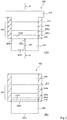
- the figure 1 is a simplified perspective view of an exemplary phase change memory device 10 comprising a plurality of memory cells 100.
- Phase change memory cells such as memory cells 100 shown in figure 1
- NVM non-volatile memory
- EEPROMs electrically erasable programmable read-only memories
- the memory cells 100 of the memory device 10 are arranged in a pattern in the form of a grid or a matrix.
- the memory device 10 is composed of an array of memory cells 100.
- Each memory cell 100 is disposed at the intersection of a row and a column of the array.
- figure 1 only three columns BL and two rows WL are shown.
- bit lines bit lines
- word lines word lines
- Each phase change memory cell 100 of memory device 10 includes a heater 102 or resistive element.
- the heating element 102 has an L-shaped cross section and therefore comprises a horizontal part and a vertical part.
- the heating element 102 is generally surrounded by an insulating or dielectric layer 104, which is for example composed of nitride and / or oxide, for example silicon oxide or silicon nitride.
- the thickness of this insulating layer 104 is such that the upper surface 1022 of the vertical part of the heating element 102 is coplanar with the upper surface 1040 of the insulating layer 104.
- Each memory cell 100 further comprises a layer 106.
- This layer 106 is made of a phase change material. Layer 106 is formed and sits on both top surface 1040 of insulating layer 104 and top surface 1022 of the vertical portion of heater 102.
- a conductive metal layer 108 rests on top of the layer 106. This conductive layer 108 typically forms an electrode of the memory cell 100.
- memory cells 100 belonging to a given bit line share the same insulating layer 104, the same layer 106 and the same conductive layer 108.
- the layers 104, 106 and 108 thus extend laterally in the direction BL (to the left and to the right, in figure 1 ). All of the memory cells 100 of a given bit line therefore share a common electrode 108.
- Conductive vias 110 are provided to connect each electrode 108 to a metallization level located above the memory cells 100 of the memory device 10.
- each memory cell 100 is typically connected, by its foot 1020 (that is to say a lower surface of its horizontal part), to a lower contact 112 or pillar.
- This lower contact 112 extends vertically and is connected to a substrate 114.
- the substrate 114 also has shallow trench insulations (STI) 116 between the portions of the substrate in contact with the lower contacts 112 belonging to adjacent bit lines. These shallow trench insulations 116 prevent the leakage of electric current between different bit lines of the memory device 10. In the memory device 10, the shallow trench insulations 116 thus extend laterally in the direction BL (to the left. and to the right, in figure 1 ).
- STI shallow trench insulations
- each memory cell 100 is connected to a terminal of a selection element.
- the element selection often called a selector or access device, provides the ability to individually address / select each memory cell 100 of the memory device 10.
- the selector of a memory cell 100 is a transistor whose gate 118 receives a bias voltage. Depending on its value, this bias voltage allows the activation or deactivation of a current between the electrode 108 and a conductive region 120 connected to the other terminal of the selection element and to a common reference potential. , typically a ground potential.
- the selection transistors of the memory cells 100 belonging to a given word line or row share the same gate 118.
- the gates 118 and the region 120 thus extend longitudinally in the direction WL (towards the forward and backward, figure 1 ). All the selection transistors of the memory cells 100 of a given word line are consequently connected to the same gate 118.
- Conductive layers 108 and gates 118 therefore both form a matrix or grid-like pattern, in which each intersection is roughly aligned vertically with a memory cell 100.
- Layer 106 is found to be natively, i.e. after fabrication of memory cell 100 and before write / program operations start, either in a fully crystalline state / phase or in a state / phase. partially crystalline state / phase. It is usual to carry out a first electrical operation to put the layer 106 of all the memory cells in an entirely crystalline state / phase. We will suppose, for example, that this crystalline phase corresponds to the logical value 1. In the memory phase change 10 consisting of a plurality of memory cells 100, an initial state thus corresponds to a state where all the memory cells 100 have the same value 1. The storage of data in the phase change memory 10 is then carried out by writing / programming some of its memory cells 100, while other cells of its memory cells 100 are left in their state (i.e. in a crystalline state).
- this memory cell 100 is first selected by applying an appropriate voltage bias to the associated gate 118. An electric current is then passed through. through layer 106 by applying an appropriate electrical potential pulse between the associated electrode 108 and the common ground region 120. The electrical potential or intensity of this electrical current is carefully adjusted to sufficiently increase the temperature of the element. heater 102 to Joule heat a region of layer 106 in contact with upper end 1022 of heater 102. This causes at least part of the phase change material, including the layer, to melt. 106 is incorporated.
- the falling edge of the potential pulse is steep, at the end of the pulse, the flow of electric current is quickly terminated and, as a result, the local temperature decreases rapidly, which achieves a hardening of the glassy structure of the molten part of the phase change material.
- the electric pulse transformed part of the phase change material from a low resistive crystalline phase to a high resistive amorphous state. For example, it will be assumed that this amorphous state corresponds to the logical value 0.
- this memory cell 100 is first selected by applying an appropriate voltage bias to the associated gate 118.
- a current the value of which is sufficiently low to avoid any unintentional phase change, is then passed through the cell 100 by applying an appropriate electrical potential between the associated electrode 108 and the common ground region 120.
- An electrical resistance, between electrode 108 and heating element 102, can then be measured. This electrical resistance reflects the value, 0 or 1, which was previously stored in memory cell 100.
- a drawback of the memory device 10 described in figure 1 comes from the fact that the layer 106 does not belong only to a single memory cell 100, but is also shared by all the memory cells 100 of the same bit line. This can lead to problems during programming of a given memory cell 100, due to lateral thermal diffusion which can disturb the amorphous state of adjacent cells of the same bit line. It can also lead to problems during reading of a given memory cell 100, since alternate current flow paths are easily provided by adjacent memory cells 100 of the same bit line. These problems are often referred to as "crosstalk" phenomena between adjacent memory cells.
- Another drawback of the memory cell 100 shown in figure 1 is that only two memory states (typically corresponding to a fully crystalline state and a fully amorphous state) can be easily obtained with such a cell. In other words, a single bit of information can be easily stored in a memory cell 100. This is due to the fact that states Possible intermediates are not stable since they are subjected to a resistance drift phenomenon, which typically leads to an increase in resistance over time.
- the design of the memory cell 100 is modified in order to at least partially overcome the aforementioned drawbacks of known phase change memory cells.
- the figure 2 shows two simplified sectional views (A) and (B) of an embodiment of a phase change memory cell 200 resulting from a manufacturing step.
- View (B) is a sectional view, along a section plane B-B, of the memory cell 200 shown in view (A).
- the phase change memory cell 200 includes a heating element or resistive element 202.
- the heating element 202 has, as shown in view (A), an L-shaped cross section. This heating element 202 is connected, by its foot 2020 (that is to say a lower surface of its horizontal part), to a selection element (not shown in figure 2 ), for example a transistor.
- the selection element provides the ability to individually address / select each memory cell 200 in a memory device comprising an array of memory cells 200.
- the heating element 202 is surrounded by an insulating layer 204.
- the thickness of this insulating layer 204 is such that the upper surface 2022 of the vertical part of the heating element 202 is coplanar with the upper surface 2040 of the insulating layer. 204.
- the selection element (not shown in figure 2 ) is located below the insulating layer 204 and is electrically connected to the foot 2020 of the heating element 202.
- the first alloy is a stable alloy, that is to say an alloy in which the proportions of the various components are close to a stoichiometric proportion.
- the first alloy is for example Ge 2 Sb 2 Te 5 , Ge 4 Sb 4 Te 7 or an alloy consisting of germanium, antimony and tellurium with atomic percentages close to, and for example substantially equal to the atomic percentages of Ge 2 Sb 2 Te 5 or Ge 4 Sb 4 Te 7 .
- the first alloy of layers 206b is preferably in a crystalline phase.
- the layers 206a are, for example, of undoped germanium or of germanium doped with nitrogen atoms. In the case where the layers 206a are made of germanium doped with nitrogen atoms, the nitrogen content is preferably less than 35% of the atom count.
- the material of the layer 206a is for example in an amorphous phase.
- the layers of the stack 206 have for example a thickness greater than approximately 4 nm, for example between 4 and 30 nm.
- the layers 206a and 206b can be of different thicknesses.
- the stack 206 comprises at least one germanium layer 206a and at least one layer 206b made of the first alloy.
- Layer 206b preferably covers layer 206a.
- the stack 206 comprises a layer 206a located between two layers 206b made of the first alloy.
- Stack 206 can include any number of layers, greater than two. The number of layers can be odd or even.
- the lower layer of stack 206 may be a germanium layer 206a or a layer 206b made from the first alloy.
- a conductive layer 208 rests on and is in contact with the stack 206, more particularly with the upper layer of the stack (one of the layers 206b, in the example of figure 2 ).
- This conductive layer 208 typically forms an electrode (to be connected to the bit line) of the memory cell 200, while the heating element 202 forms another electrode (to be connected to the word line) of the memory cell 200.
- two electrodes are also referred to herein as "upper" electrode 208 and "lower” electrode 202, although no limitation is implied as to the orientation of memory cell 200 in operation.
- the upper part of the upper electrode 208 extends horizontally in a direction orthogonal to the section plane BB.
- the heating element 202 is preferably centered relative to the memory cell 200.
- the resistive layer 210 extends below the entire lower layer of the stack 206.
- the side walls of memory cell 200 are surrounded by an insulating region 212. All four side faces of stack 206 and of resistive layer 210 are, as shown in views (A) and (B), completely enclosed / enveloped by this insulating region 212, although only part of the conductive layer 208 is flanked by the insulating region 212.
- a memory device (not shown in figure 2 ) consisting of a matrix of memory cells 200, this allows the upper electrode 208 to be connected to the stack 206 of other memory cells 200 of the same bit line.
- the memory cell described in relation to the figure 2 corresponds to an intermediate state in the manufacturing process of the memory cell.
- a following step, corresponding to a "training" step is described in relation to the figure 3 .
- the figure 3 shows two simplified sectional views (A) and (B) of an embodiment of a phase change memory cell resulting from a subsequent manufacturing step.
- View (B) is a sectional view, along a section plane B-B, of the memory cell 200 shown in view (A).
- the step resulting in the memory cell 200 of the figure 3 comprises an electrical operation called "training" performed after the step resulting in the memory cell of the figure 2 .
- a strong current pulse typically larger than the pulses normally applied to program memory cells, flows between the upper electrode 208 and the lower electrode 202 and passes through the resistive layer 210 and the stack 206 .
- Part 214 rests on the upper surface of layer 210. Part 214 is thus in electrical contact with resistive element 202, through resistive layer 210.
- Part 214 has the shape of a dome, in in other words it has a cross section substantially in the form of a semicircle, or of a circular part, centered on the region of contact between the resistive element 202 and the resistive layer 210.
- the part 214 is centered on the region. of contact between the resistive element 202 and the resistive layer 210 regardless of the position of the contact region. Therefore, misalignment issues relating to the formation of resistive element 202 are negligible, as long as the resistive element is in contact with resistive layer 210.
- the region 214 does not reach the layer 208.
- the upper part of the region 214 is separated from the layer 208 by a part of the layer 206b. More generally, the upper part of the region 214 can be separated from the layer 208 by a part made of the first alloy.
- the upper part of region 214 in other words the part of region 214 closest to layer 208, is not separated from layer 208 by a germanium layer.
- region 214 can reach layer 208.
- Part 214 is made of a second alloy consisting of germanium, antimony and tellurium, the germanium concentration of the second alloy being greater than that of the first alloy.
- the second alloy is, like the first alloy, a phase change material, as described above.
- the proportions of the components of the second alloy for example, are not stoichiometric.
- the proportion of germanium in the second alloy is for example between 1.5 times and 3.5 times the proportion of germanium in the first alloy.
- the quantity of germanium in the second alloy depends on the quantity of germanium in the heated parts, that is to say on the number and the thickness of the germanium layers 206a, relative to the quantity of the first alloy.
- the data written, or programmed, in the memory cell is determined by the amorphous or crystalline phase of at least a portion of part 214.
- An example of the programming method will be described in relation to the figure 4 .
- the memory cell 200 is referred to as a "completely confined cell".
- the insulating region 212 in fact behaves as a galvanic isolation but also as a thermal barrier separating adjacent cells, thus avoiding interference between cells.
- the phenomenon of crosstalk between adjacent memory cells which has already been described with reference to the figure 1 , theoretically cannot occur in a completely confined memory cell like the memory cell 200 shown in the figures 2 and 3 .
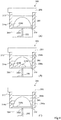
- the figure 4 shows three simplified sectional views (A), (B) and (C), of various steps of a method of writing in a phase change memory cell such as the memory cell described in relation to the figure 3 .
- View (A) shows a PCM cell similar to the aforementioned memory cell 200, the region 214 of which has a fully crystalline phase / structure.
- region 214 is, in view (A), entirely made up of a phase / crystal region 214a. This is the case, for example before the start of the write operations in the memory cell 200.
- a voltage is applied between the upper electrode 208 (conductive layer) and the lower electrode 202 (heating element). This voltage gives rise to an electric current flowing through region 214, which initially consists entirely of crystal phase 214a, and, if region 214 does not reach upper electrode 208, through part of the crystal phase. layer 206b located between region 214 and electrode 208.
- the memory cell 200 is thus heated, by the heating element 202, to a temperature sufficient to make at least part of the crystalline region 214 amorphous.
- the Joule heating due to the electric current flowing through the memory cell 200 causes a phase change of part of the region 214, thereby forming an amorphous region 214b above the memory cell.
- Amorphous region 214b forms a dome, which is vertically aligned with top surface 2022 of the vertical portion of heater 202, which is centered relative to memory cell 200.
- the second alloy from the amorphous region 214b located directly above the heater element 202 has phase shifted / switched, due to heating, from a crystalline phase to an amorphous state.
- the amorphous region 214b only partially covers, in view (B), the upper surface 2100 of the resistive layer 210 (i.e. the surface of the resistive layer 210 which contacts the region 214).
- region 214 therefore consists of both amorphous region 214b, where the phase change has taken place upon heating, and crystalline phase 214a, where the phase change n ' has not yet occurred.
- a memory cell such as the memory cell 200 shown in Fig. (B) is selected for reading is if the appropriate bias voltage is applied between the upper electrode 208 and the lower electrode 202, electric current flows through it.
- the electric current flows in two parallel paths (not shown in figure 2 ) so as to bypass the amorphous region 214b.
- Each of these two paths comprises one of the two branches of the portion of the resistive layer 210, these branches extending in an opposite direction from the upper surface 2022 of the heating element 202, and are covered by the region amorphous 214b.
- regions 214a and 214b are centered on heater element 202, these two paths have equivalent electrical resistance.
- the resistivity and the thickness of the resistive layer 210 are such that the resistance of the memory cell 200 in the state shown in view (B) is greater than the resistance of the memory cell 200 in the state shown in view (A ). Further, since the resistance of the resistive layer 210 is stable over time, the cell in the state shown in view (B) is almost free from the problem of resistance drift.
- the extent of the portion of the resistive layer 210 covered by the amorphous region 214b also expands and its resistance increases, roughly in proportion to the length of the portion of the 2100 surface which is covered by the amorphous region. 214b. Therefore, the resistance of the cell also increases. This allows multi-level cell programming, with analog precision, and resistance values that are stable over time (no drift).
- the stack comprises at least one layer 206a.
- Layer 206a has high resistance, and therefore low conductivity. Since layer 206a extends opposite the whole of the resistive layer 210 to the outside of the region 214, there is no conductive path in the stack 206. There is substantially no conductive path remaining between the upper electrode 208 and the lower electrode 202.
- the two electrodes 202, 208 are therefore completely isolated from each other thanks to the insulating region 212 and to the amorphous regions 214b and 206a.
- the memory cell 200 a number of memory states greater than two, namely three memory states such as represented in figure 4 . This allows for a high density of information storage in memory devices (not shown) comprising a plurality of PCM cells 200.
- the resistance of the memory cell 200 increases monotonically by increasing the part of the amorphous region 214b which covers the upper surface. 2100 of resistive layer 210.
- the resistance of the state shown in view (B) can therefore be analog modulated by increasing the program current, multiple logic levels, for digital memory, and / or storage analog, can be considered for this memory state, between the two extreme memory states represented respectively in views (A) and (C).
- the figure 5 represents the resistance corresponding to several states of the phase change memory cell. More precisely, the figure 5 represents the resistance (R) between the upper electrode 208 and the lower electrode 202, as a function of the programming current (I prog ) flowing through the region 214, between the upper electrode 208 and the lower electrode 202 for a period of programming step.
- the curve of resistance R comprises three plates 400, 402 and 404. Each plate corresponds to at least one value stored by the phase change memory cell.
- the plate 400 corresponds to a programming current between 0 and a current value I1.
- the resistance R corresponding to this current range is substantially constant and substantially equal to a resistance value R1.
- the plateau 400 corresponds to a region 214 entirely in the crystalline phase, as shown in view (A) of the figure 4 .
- the temperature generated by the resistive element 202 and the resistive layer 210 is not high enough to change the phase of the region 214.
- the region 214 does not include of amorphous region 214b. Therefore, the measurement, between the upper electrode 208 and the lower electrode 202 of a resistance substantially equal to R1 means that the memory cell is in the first memory state.
- the plate 402 corresponds to a programming current between a value I2 and a value I3.
- the resistance R corresponding to this current range increases monotonically from a value R2 to a value R3.
- the plateau 402 corresponds to a region 214 partially in a crystalline phase and partially in an amorphous phase, as shown in view (B) of the figure 4 .
- the temperature generated by resistive element 202 and resistive layer 210 is high enough to change the phase of part of region 214.
- region 214 includes the amorphous region 214b. Consequently, the measurement between the upper electrode 208 and lower electrode 202 of a resistance between R2 and R3 means that the memory cell is in the second memory state.
- the second memory state corresponds either to a single stored value, different from the stored value of the first memory state, or to multiple logic levels obtained by analogously modulating the resistance between the values R2 and R3.
- the plate 404 corresponds to a programming current greater than a current value I4.
- the resistance R corresponding to this current range is substantially constant and substantially equal to a resistance value R4.
- Plateau 404 corresponds to a region 214 entirely in the amorphous phase, as shown in view (C) of figure 4 .
- the temperature generated by the resistive element 202 and the resistive layer 210 is high enough to change the phase of the whole of region 214.
- region 214 does not include crystalline region 214a. Consequently, the measurement between the upper electrode 208 and the lower electrode 202 of a resistance substantially equal to R4 means that the memory cell is in the third memory state.
- the resistance values between R1 and R2 and between R3 and R4, corresponding respectively to a programming current between I1 and I2 and between I3 and I4, do not correspond to a memory state. In other words, if the resistance R between the upper electrode 208 and the lower electrode 202 is between R1 and R2 or between R3 and R4, there is no value stored in the memory cell. These current values are not used to program the memory cell.
- the slope of the plate 402 is for example less than 5.
- the slopes of the plates 400 and 404 are for example less than 2.
- the slope of the region corresponding to resistance values between R1 and R2 is for example included between 2 and 5 and the slope of the region corresponding to resistance values between R3 and R4 is for example greater than 5. This difference in slope makes it possible to distinguish the various regions of the curve, and consequently the various memory states.
- the current value I4 is greater than the current value I3.
- the current value I3 is greater than the current value I2.
- the current value I2 is greater than the current value I1.
- the value of resistor R4 is greater than the value of resistor R3.
- the value of resistance R3 is greater than the value of resistance R2.
- the value of resistance R2 is greater than the value of resistance R1.
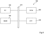
- the figure 6 schematically illustrates an embodiment of a memory 500.
- Block 502 preferably includes a circuit for addressing array of memory cells 200.
- the memory devices in block 506 are not phase change memory devices, but RAMs, reprogrammable volatile memories (EEPROM, flash, etc.).
- block 506 can be omitted.
- the memory devices of the memory 500 are then only memory devices such as memory devices comprising memory cells 200.
- the memory is then entirely non-volatile memory.
- An advantage of the embodiments described here is that the value stored by the memory cell is one of at least three different values.
- the memory cell includes a state where the memory cell can take multiple logic levels obtained by analog modulating the resistance between the upper and lower electrodes.
Abstract
La présente description concerne une cellule mémoire à changement de phase (200), comprenant : un élément chauffant (202) ; un empilement (206) d'au moins une couche de germanium ou d'une couche de germanium dopé à l'azote (206a) et d'au moins une couche (206b) d'un premier alliage constitué de germanium, d'antimoine et de tellure ; et une couche résistive (210), située entre l'élément chauffant (202) et l'empilement (206).The present description relates to a phase change memory cell (200), comprising: a heater element (202); a stack (206) of at least one layer of germanium or of a layer of germanium doped with nitrogen (206a) and at least one layer (206b) of a first alloy consisting of germanium, antimony and tellurium; and a resistive layer (210), located between the heating element (202) and the stack (206).
Description
La présente description concerne de façon générale des dispositifs mémoire, et plus particulièrement des cellules mémoire à changement de phase.The present description relates generally to memory devices, and more particularly to phase change memory cells.
Les matériaux à changement de phase sont des matériaux qui peuvent commuter sous l'effet de la chaleur, entre une phase cristalline et une phase amorphe. Puisque la résistance électrique d'un matériau amorphe est notablement supérieure à la résistance électrique d'une phase cristalline du même matériau, un tel phénomène est utilisé pour définir deux états mémoire, par exemple 0 et 1, différenciés par la résistance mesurée à travers le matériau à changement de phase. Les matériaux à changement de phase les plus courants utilisés pour fabriquer des mémoires sont des alliages constitués de germanium, d'antimoine et de tellure.Phase change materials are materials which can switch under the effect of heat between a crystalline phase and an amorphous phase. Since the electrical resistance of an amorphous material is significantly greater than the electrical resistance of a crystalline phase of the same material, such a phenomenon is used to define two memory states, for example 0 and 1, differentiated by the resistance measured across the phase change material. The most common phase change materials used to make memories are alloys made of germanium, antimony and tellurium.
Il existe un besoin d'améliorer les cellules mémoire à changement de phase existantes afin d'obtenir de manière fiable un nombre d'états mémoire supérieur à deux.There is a need to improve existing phase change memory cells in order to reliably obtain a number of memory states greater than two.
Il existe un besoin d'améliorer les cellules mémoire à changement de phase existantes afin qu'elles soient moins affectées par des problèmes de défauts d'alignement.There is a need to improve existing phase change memory cells so that they are less affected by misalignment problems.
Un mode de réalisation pallie tout ou partie des inconvénients des cellules mémoire à changement de phase connues.One embodiment overcomes all or part of the drawbacks of known phase change memory cells.
Un mode de réalisation prévoit une cellule mémoire à changement de phase, comprenant : un élément chauffant ; un empilement d'au moins une couche de germanium ou d'une couche de germanium dopé à l'azote et d'au moins une couche d'un premier alliage constitué de germanium, d'antimoine et de tellure ; et une couche résistive, située entre l'élément chauffant et l'empilement.One embodiment provides a phase change memory cell, comprising: a heater element; a stack of at least one germanium layer or a layer germanium doped with nitrogen and at least one layer of a first alloy consisting of germanium, antimony and tellurium; and a resistive layer, located between the heating element and the stack.
Selon un mode de réalisation, des parois latérales de l'empilement et de la couche résistive sont entourées d'une région isolante.According to one embodiment, side walls of the stack and of the resistive layer are surrounded by an insulating region.
Selon un mode de réalisation, la couche résistive s'étend en dessous de la totalité de la couche inférieure de l'empilement.According to one embodiment, the resistive layer extends below the entire lower layer of the stack.
Selon un mode de réalisation, la couche résistive est en contact avec l'élément chauffant et la couche inférieure de l'empilement.According to one embodiment, the resistive layer is in contact with the heating element and the lower layer of the stack.
Selon un mode de réalisation, l'empilement comprend une deuxième région en un deuxième alliage constitué de germanium, d'antimoine et de tellure, la deuxième région s'étendant à partir de la couche résistive et à travers la couche de germanium ou de germanium dopé à l'azote, le deuxième alliage ayant une concentration en germanium supérieure à celle du premier alliage.According to one embodiment, the stack comprises a second region made of a second alloy consisting of germanium, antimony and tellurium, the second region extending from the resistive layer and through the germanium or germanium layer. doped with nitrogen, the second alloy having a higher germanium concentration than the first alloy.
Selon un mode de réalisation, une couche conductrice repose sur la couche supérieure de l'empilement.According to one embodiment, a conductive layer rests on the upper layer of the stack.
Selon un mode de réalisation, il n'y a aucune partie de la couche de germanium entre la partie supérieure de la région et la couche conductrice.According to one embodiment, there is no part of the germanium layer between the upper part of the region and the conductive layer.
Selon un mode de réalisation : un premier état mémoire est défini par le fait que la région est entièrement dans un état cristallin ; un deuxième état mémoire est défini par le fait qu'il comporte une région amorphe recouvrant totalement une surface supérieure de la couche résistive ; et au moins un état mémoire intermédiaire est défini par le fait que la région amorphe recouvre partiellement la surface supérieure de la couche résistive.According to one embodiment: a first memory state is defined by the fact that the region is entirely in a crystalline state; a second memory state is defined by the fact that it comprises an amorphous region completely covering an upper surface of the resistive layer; and at least one intermediate memory state is defined by the fact that the Amorphous region partially covers the top surface of the resistive layer.
Un autre mode de réalisation prévoit un procédé de fabrication de la cellule de l'une quelconque des revendications 1 à 8, comprenant une étape dans laquelle une partie de l'empilement est chauffée jusqu'à une température suffisante pour que les parties des couches de germanium ou de germanium dopé à l'azote et du premier alliage situées dans cette partie forment un deuxième alliage constitué de germanium, d'antimoine et de tellure, le deuxième alliage ayant une concentration en germanium supérieure à celle du premier alliage.Another embodiment provides a method of manufacturing the cell of any one of claims 1 to 8, comprising a step in which a portion of the stack is heated to a temperature sufficient for the portions of the layers to be germanium or germanium doped with nitrogen and the first alloy located in this part form a second alloy consisting of germanium, antimony and tellurium, the second alloy having a germanium concentration greater than that of the first alloy.
Selon un mode de réalisation, le procédé comprend une étape de chauffage de la région afin d'atteindre l'un d'au moins trois états mémoire.According to one embodiment, the method comprises a step of heating the region in order to reach one of at least three memory states.
Selon un mode de réalisation, la région est chauffée par l'intermédiaire de l'élément chauffant et de la couche résistive.According to one embodiment, the region is heated by means of the heating element and the resistive layer.
Selon un mode de réalisation, la résistance électrique de la cellule augmente de façon monotone en augmentant une partie de la région amorphe qui recouvre la surface supérieure de la couche résistive.According to one embodiment, the electrical resistance of the cell increases monotonically by increasing a part of the amorphous region which covers the upper surface of the resistive layer.
Un autre mode de réalisation prévoit un dispositif mémoire comprenant au moins une cellule mémoire telle que décrite.Another embodiment provides for a memory device comprising at least one memory cell as described.
Ces caractéristiques et avantages, ainsi que d'autres, seront exposés en détail dans la description suivante de modes de réalisation particuliers faite à titre non limitatif en relation avec les figures jointes parmi lesquelles :
- la
figure 1 est une vue en perspective simplifiée d'un exemple de dispositif mémoire à changement de phase ; - la
figure 2 représente deux vues en coupe simplifiées (A) et (B) d'un mode de réalisation d'une cellule mémoire à changement de phase résultant d'une étape de fabrication ; - la
figure 3 représente deux vues en coupe simplifiées (A) et (B) d'un mode de réalisation d'une cellule mémoire à changement de phase résultant d'une étape de fabrication à la suite de l'étape de lafigure 2 ; - la
figure 4 représente trois vues en coupe simplifiées (A), (B) et (C) de diverses étapes d'un procédé d'écriture dans une cellule mémoire à changement de phase ; - la
figure 5 est un diagramme illustrant un exemple de variations de la résistance correspondant à plusieurs états de la cellule mémoire à changement de phase ; et - la
figure 6 représente schématiquement un mode de réalisation d'une mémoire.
- the
figure 1 is a simplified perspective view of an exemplary phase change memory device; - the
figure 2 shows two simplified sectional views (A) and (B) of an embodiment of a phase change memory cell resulting from a manufacturing step; - the
figure 3 shows two simplified sectional views (A) and (B) of an embodiment of a phase change memory cell resulting from a manufacturing step following the manufacturing step.figure 2 ; - the
figure 4 shows three simplified sectional views (A), (B) and (C) of various steps of a method of writing in a phase change memory cell; - the
figure 5 is a diagram illustrating an example of variations of the resistance corresponding to several states of the phase change memory cell; and - the
figure 6 schematically represents an embodiment of a memory.
De mêmes éléments ont été désignés par de mêmes références dans les différentes figures. En particulier, les éléments structurels et/ou fonctionnels communs aux différents modes de réalisation peuvent présenter les mêmes références et peuvent disposer de propriétés structurelles, dimensionnelles et matérielles identiques.The same elements have been designated by the same references in the various figures. In particular, the structural and / or functional elements common to the different embodiments may have the same references and may have identical structural, dimensional and material properties.
Par souci de clarté, seuls les étapes et éléments utiles à la compréhension des modes de réalisation décrits ont été représentés et sont détaillés.For the sake of clarity, only the steps and elements useful for understanding the embodiments described have been shown and are detailed.
Sauf précision contraire, lorsque l'on fait référence à deux éléments connectés entre eux, cela signifie directement connectés sans éléments intermédiaires autres que des conducteurs, et lorsque l'on fait référence à deux éléments couplés entre eux, cela signifie que ces deux éléments peuvent être connectés ou être reliés par l'intermédiaire d'un ou plusieurs autres éléments.Unless otherwise specified, when referring to two elements connected together, it means directly connected without intermediate elements other than conductors, and when referring to two elements coupled together, it means that these two elements can be connected or be linked through one or more other elements.
Dans la description qui suit, lorsque l'on fait référence à des qualificatifs de position absolue, tels que les termes "avant", "arrière", "haut", "bas", "gauche", "droite", etc., ou relative, tels que les termes "dessus", "dessous", "supérieur", "inférieur", etc., ou à des qualificatifs d'orientation, tels que les termes "horizontal", "vertical", etc., il est fait référence sauf précision contraire à l'orientation des figures.In the following description, when reference is made to absolute position qualifiers, such as the terms "front", "rear", "top", "bottom", "left", "right", etc., or relative, such as the terms "above", "below", "upper", "lower", etc., or to orientation qualifiers, such as the terms "horizontal", "vertical", etc., it reference is made unless otherwise specified in the orientation of the figures.
Sauf précision contraire, les expressions "environ", "approximativement", "sensiblement" et "de l'ordre de" signifient à 10 % près, de préférence à 5 % près.Unless otherwise specified, the expressions "approximately", "approximately", "substantially" and "of the order of" mean within 10%, preferably within 5%.
La
Les cellules mémoire à changement de phase (PCM), telles que les cellules mémoire 100 représentées en
Comme cela est représenté en
Les colonnes BL, qui sont parallèles entre elles et parallèles au plan de la
Chaque cellule mémoire à changement de phase 100 du dispositif mémoire 10 comprend un élément chauffant 102 ou élément résistif. Dans l'exemple de la
L'élément chauffant 102 est en général entouré d'une couche isolante ou diélectrique 104, qui est par exemple composée de nitrure et/ou d'oxyde, par exemple d'oxyde de silicium ou de nitrure de silicium. L'épaisseur de cette couche isolante 104 est telle que la surface supérieure 1022 de la partie verticale de l'élément chauffant 102 est coplanaire avec la surface supérieure 1040 de la couche isolante 104.The
Chaque cellule mémoire 100 comprend en outre une couche 106. Cette couche 106 est en un matériau à changement de phase. La couche 106 est formée et repose à la fois sur la surface supérieure 1040 de la couche isolante 104 et sur la surface supérieure 1022 de la partie verticale de l'élément chauffant 102.Each
Une couche métallique conductrice 108 repose sur le dessus de la couche 106. Cette couche conductrice 108 forme typiquement une électrode de la cellule mémoire 100.A
Dans l'exemple de la
L'élément chauffant 102 de chaque cellule mémoire 100 est typiquement connecté, par son pied 1020 (c'est-à-dire une surface inférieure de sa partie horizontale), à un contact inférieur 112 ou pilier. Ce contact inférieur 112 s'étend verticalement et est connecté à un substrat 114.The
Dans l'exemple de la
- une première couche 1140 constituée d'un film mince de silicium, auquel les contacts inférieurs 112 sont connectés ;
- une deuxième couche 1142 constituée d'oxyde mince enterré ; et
- une troisième couche 1144 constituée d'une tranche de silicium épais.
- a
first layer 1140 made of a thin film of silicon, to which thelower contacts 112 are connected; - a
second layer 1142 made of buried thin oxide; and - a
third layer 1144 consisting of a thick silicon wafer.
Le substrat 114 présente aussi des isolations par tranchées peu profondes (STI) 116 entre les parties du substrat en contact avec les contacts inférieurs 112 appartenant à des lignes de bit adjacentes. Ces isolations par tranchées peu profondes 116 empêchent la fuite de courant électrique entre des lignes de bit différentes du dispositif mémoire 10. Dans le dispositif mémoire 10, les isolations par tranchées peu profondes 116 s'étendent ainsi latéralement suivant la direction BL (vers la gauche et vers la droite, en
Le contact inférieur 112 de chaque cellule mémoire 100 est connecté à une borne d'un élément de sélection. L'élément de sélection, souvent appelé sélecteur ou dispositif d'accès, assure la capacité à adresser/sélectionner individuellement chaque cellule mémoire 100 du dispositif mémoire 10. Dans l'exemple de la
Dans l'exemple de la
Les couches conductrices 108 et les grilles 118 forment par conséquent toutes deux un motif en forme de matrice ou de grille, dans lequel chaque intersection est à peu près alignée verticalement avec une cellule mémoire 100.
Il se trouve que la couche 106 est de manière native, c'est-à-dire après la fabrication de la cellule mémoire 100 et avant le début des opérations d'écriture/programmation, soit dans un état/phase entièrement cristallin soit dans un état/phase partiellement cristallin. Il est usuel de réaliser une première opération électrique pour mettre la couche 106 de toutes les cellules mémoire dans un état/phase entièrement cristallin. On supposera, par exemple, que cette phase cristalline correspond à la valeur logique 1. Dans la mémoire à changement de phase 10 constituée d'une pluralité de cellules mémoire 100, un état initial correspond ainsi à un état où toutes les cellules mémoire 100 ont la même valeur 1. La mémorisation de données dans la mémoire à changement de phase 10 est alors réalisée en écrivant/programmant certaines de ses cellules mémoire 100, tandis que d'autres cellules de ses cellules mémoire 100 sont laissées dans leur état (c'est-à-dire dans un état cristallin).
Pour écrire dans, ou programmer, une cellule mémoire à changement de phase 100 donnée de la mémoire 10, cette cellule mémoire 100 est d'abord sélectionnée en appliquant une polarisation en tension appropriée à la grille associée 118. On fait passer ensuite un courant électrique à travers la couche 106 en appliquant une impulsion de potentiel électrique appropriée entre l'électrode 108 associée et la région de masse commune 120. Le potentiel électrique ou l'intensité de ce courant électrique est soigneusement ajusté pour augmenter suffisamment la température de l'élément chauffant 102 pour chauffer, par effet Joule, une région de la couche 106 en contact avec l'extrémité supérieure 1022 de l'élément chauffant 102. Cela provoque la fusion d'au moins une partie du matériau à changement de phase, dont la couche 106 est constituée. Si le front descendant de l'impulsion de potentiel est abrupte, à la fin de l'impulsion, le flux de courant électrique se termine rapidement et, en conséquence, la température locale diminue rapidement, ce qui réalise une trempe de la structure vitreuse de la partie fondue du matériau à changement de phase. En résultat, l'impulsion électrique a transformé une partie du matériau à changement de phase d'une phase cristalline faiblement résistive en un état amorphe fortement résistif. On supposera par exemple que cet état amorphe correspond à la valeur logique 0.To write into, or program, a given phase
Pour lire une cellule mémoire à changement de phase 100 donnée, cette cellule mémoire 100 est d'abord sélectionnée en appliquant une polarisation en tension appropriée à la grille 118 associée. On fait ensuite passer un courant, dont la valeur est suffisamment faible pour éviter tout changement de phase involontaire, à travers la cellule 100 en appliquant un potentiel électrique approprié entre l'électrode 108 associée et la région de masse commune 120. Une résistance électrique, entre l'électrode 108 et l'élément chauffant 102, peut alors être mesurée. Cette résistance électrique reflète la valeur, 0 ou 1, qui était précédemment mémorisée dans la cellule mémoire 100.To read a given phase
Un inconvénient du dispositif mémoire 10 décrit en
Un autre inconvénient de la cellule mémoire 100 représentée en
Selon les modes de réalisation décrits ci-après, la conception de la cellule mémoire 100 est modifiée afin de pallier au moins en partie les inconvénients susmentionnés des cellules mémoire à changement de phase connues.According to the embodiments described below, the design of the
La
La vue (B) est une vue en coupe, selon un plan de coupe B-B, de la cellule mémoire 200 représentée en vue (A).View (B) is a sectional view, along a section plane B-B, of the
La cellule mémoire à changement de phase 200 comprend un élément chauffant ou élément résistif 202. L'élément chauffant 202 a, comme cela est représenté en vue (A), une section transversale en forme de L. Cet élément chauffant 202 est connecté, par son pied 2020 (c'est-à-dire une surface inférieure de sa partie horizontale), à un élément de sélection (non représenté en
L'élément chauffant 202 est entouré d'une couche isolante 204. L'épaisseur de cette couche isolante 204 est telle que la surface supérieure 2022 de la partie verticale de l'élément chauffant 202 est coplanaire avec la surface supérieure 2040 de la couche isolante 204. L'élément de sélection (non représenté en
La cellule mémoire 200 comprend un empilement 206 de couches 206a en germanium ou en germanium dopé à l'azote et de couches 206b en un premier alliage de germanium, d'antimoine et de tellure. Les couches de l'empilement 206 sont alternativement des couches 206a et des couches 206b.The
Dans le mode de réalisation de la
Le premier alliage est un alliage stable, c'est-à-dire un alliage dans lequel les proportions des divers composants sont proches d'une proportion stœchiométrique. Le premier alliage est par exemple Ge2Sb2Te5, Ge4Sb4Te7 ou un alliage constitué de germanium, d'antimoine et de tellure avec des pourcentages atomiques proches de, et par exemple sensiblement égaux aux pourcentages atomiques de Ge2Sb2Te5 ou Ge4Sb4Te7. Le premier alliage des couches 206b est de préférence dans une phase cristalline. Les couches 206a sont par exemple en germanium non dopé ou en germanium dopé avec des atomes d'azote. Dans le cas où les couches 206a sont en germanium dopé avec des atomes d'azote, le contenu en azote est de préférence inférieur à 35 % du compte d'atomes. Le matériau de la couche 206a est par exemple dans une phase amorphe.The first alloy is a stable alloy, that is to say an alloy in which the proportions of the various components are close to a stoichiometric proportion. The first alloy is for example Ge 2 Sb 2 Te 5 , Ge 4 Sb 4 Te 7 or an alloy consisting of germanium, antimony and tellurium with atomic percentages close to, and for example substantially equal to the atomic percentages of Ge 2 Sb 2 Te 5 or Ge 4 Sb 4 Te 7 . The first alloy of
Les couches de l'empilement 206 ont par exemple une épaisseur supérieure à environ 4 nm, par exemple comprise entre 4 et 30 nm. Les couches 206a et 206b peuvent être d'épaisseurs différentes.The layers of the
Dans certains modes de réalisation, les diverses couches 206b sont en des alliages différents de germanium, d'antimoine et de tellure choisis parmi les exemples donnés précédemment pour le premier alliage. Par exemple, l'empilement 206 peut comprendre une couche 206a en germanium située entre une couche 206b en Ge2Sb2Te5 et une couche 206b en Ge4Sb4Te7. Ces différents alliages seront néanmoins appelés premier alliage dans la description qui suit.In certain embodiments, the
Plus généralement, l'empilement 206 comprend au moins une couche de germanium 206a et au moins une couche 206b faite du premier alliage. La couche 206b recouvre de préférence la couche 206a. De préférence, l'empilement 206 comprend une couche 206a située entre deux couches 206b faites du premier alliage. L'empilement 206 peut comprendre un nombre quelconque de couches, supérieur à deux. Le nombre de couches peut être pair ou impair. En outre, la couche inférieure de l'empilement 206 peut être une couche de germanium 206a ou une couche 206b faite du premier alliage.More generally, the
Une couche conductrice 208 repose sur et est en contact avec l'empilement 206, plus particulièrement avec la couche supérieure de l'empilement (l'une des couches 206b, dans l'exemple de la
Dans l'exemple de la vue (A), la partie supérieure de l'électrode supérieure 208 s'étend horizontalement suivant une direction orthogonale au plan de coupe BB. L'élément chauffant 202 est de préférence centré par rapport à la cellule mémoire 200.In the example of view (A), the upper part of the
Selon un mode de réalisation préféré, une couche résistive 210 est intercalée entre la couche isolante 204 et l'empilement 206. En d'autres termes :
- la couche résistive 210 est formée et repose à la fois sur la
surface supérieure 2040 de la couche isolante 204 et sur lasurface supérieure 2022 de la partie verticale de l'élément chauffant 202, la couche 210 étant en contact électrique avec l'élément chauffant 202 ; et l'empilement 206 est formé et repose sur lasurface supérieure 2100 de la couche résistive 210.
- the
resistive layer 210 is formed and rests on both theupper surface 2040 of the insulatinglayer 204 and theupper surface 2022 of the vertical portion of theheating element 202, thelayer 210 being in electrical contact with theheating element 202; and - the
stack 206 is formed and rests on theupper surface 2100 of theresistive layer 210.
De préférence, la couche résistive 210 s'étend en dessous de la totalité de la couche inférieure de l'empilement 206.Preferably, the
La couche résistive 210 est par exemple en un métal réfractaire et/ou un nitrure de métal réfractaire, comme le nitrure de titane (TiN), le tantale (Ta), le nitrure de tantale (TaN) ou le tungstène (W).The
Les parois latérales de la cellule mémoire 200 sont entourées d'une région isolante 212. Toutes les quatre faces latérales de l'empilement 206 et de la couche résistive 210 sont, comme cela est représenté dans les vues (A) et (B), totalement enfermées/enveloppées par cette région isolante 212, bien que seulement une partie de la couche conductrice 208 soit flanquée de la région isolante 212. Dans un dispositif mémoire (non représenté en
La cellule mémoire décrite en relation avec la
La
La vue (B) est une vue en coupe, selon un plan de coupe B-B, de la cellule mémoire 200 représentée en vue (A).View (B) is a sectional view, along a section plane B-B, of the
L'étape ayant pour résultat la cellule mémoire 200 de la
L'élément résistif 202 chauffe jusqu'à atteindre une température qui est par exemple supérieure à 600 °C, de préférence supérieure à 900 °C, afin de faire fondre une partie des matériaux des couches 206a et 206b. Cette opération forme une partie 214 en un alliage riche en Ge homogène, à partir des parties fondues des couches 206a et 206b. La partie 214 est la zone active de la mémoire à changement de phase. De préférence, l'opération de "formation" est réalisée de telle manière que la partie 214 est dans la phase cristalline à la fin de l'opération.The
La partie 214 repose sur la surface supérieure de la couche 210. La partie 214 est ainsi en contact électrique avec l'élément résistif 202, par l'intermédiaire de la couche résistive 210. La partie 214 a la forme d'un dôme, en d'autres termes elle a une section transversale sensiblement en forme de demi-cercle, ou d'une partie circulaire, centrée sur la région de contact entre l'élément résistif 202 et la couche résistive 210. La partie 214 est centrée sur la région de contact entre l'élément résistif 202 et la couche résistive 210 quelle que soit la position de la région de contact. Par conséquent, les problèmes de défauts d'alignement concernant la formation de l'élément résistif 202 sont négligeables, tant que l'élément résistif est en contact avec la couche résistive 210.
Dans l'exemple de la
La partie 214 est en un deuxième alliage constitué de germanium, d'antimoine et de tellure, la concentration en germanium du deuxième alliage étant supérieure à celle du premier alliage. Le deuxième alliage est, comme le premier alliage, un matériau à changement de phase, comme ce qui a été décrit précédemment. Les proportions des composants du deuxième alliage par exemple ne sont pas stœchiométriques. La proportion de germanium dans le deuxième alliage est par exemple comprise entre 1,5 fois et 3,5 fois la proportion de germanium dans le premier alliage.
La quantité de germanium dans le deuxième alliage dépend de la quantité de germanium dans les parties chauffées, c'est-à-dire du nombre et de l'épaisseur des couches de germanium 206a, par rapport à la quantité du premier alliage.The quantity of germanium in the second alloy depends on the quantity of germanium in the heated parts, that is to say on the number and the thickness of the
Les données écrites, ou programmés, dans la cellule mémoire sont déterminées par la phase amorphe ou cristalline d'au moins une portion de la partie 214. Un exemple du procédé de programmation va être décrit en relation avec la
En raison de la présence de la région isolante 212, la cellule mémoire 200 est appelée "cellule complètement confinée". Dans une matrice mémoire à changement de phase (non représentée), la région isolante 212 se comporte en effet comme une isolation galvanique mais aussi comme une barrière thermique séparant des cellules adjacentes, évitant ainsi des interférences entre cellules. Le phénomène de diaphonie entre cellules mémoire adjacentes, qui a déjà été décrit en référence avec la
La
La vue (A) représente une cellule PCM similaire à la cellule mémoire 200 susmentionnée, dont la région 214 présente une phase/structure entièrement cristalline. En d'autres termes, la région 214 est, dans la vue (A), entièrement constituée d'une phase/région cristalline 214a. C'est le cas, par exemple avant le début des opérations d'écriture dans la cellule mémoire 200.View (A) shows a PCM cell similar to the
Pour écrire dans la cellule mémoire 200, une tension est appliquée entre l'électrode supérieure 208 (couche conductrice) et l'électrode inférieure 202 (élément chauffant). Cette tension donne naissance à un courant électrique s'écoulant à travers la région 214, qui est initialement entièrement constituée de la phase cristalline 214a, et, si la région 214 n'atteint pas l'électrode supérieure 208, à travers une partie de la couche 206b située entre la région 214 et l'électrode 208. La cellule mémoire 200 est ainsi chauffée, par l'élément chauffant 202, jusqu'à une température suffisante pour rendre amorphe au moins une partie de la région cristalline 214.To write to the
Dans la vue (B), le chauffage par effet Joule dû au courant électrique s'écoulant à travers la cellule mémoire 200 provoque un changement de phase d'une partie de la région 214, formant ainsi une région amorphe 214b au-dessus de la surface supérieure 2100 de la couche résistive 210. La région amorphe 214b forme un dôme, qui est aligné verticalement avec la surface supérieure 2022 de la partie verticale de l'élément chauffant 202, qui est centrée par rapport à la cellule mémoire 200.In view (B), the Joule heating due to the electric current flowing through the
Le deuxième alliage de la région amorphe 214b située directement au-dessus de l'élément chauffant 202 a changé/commuté de phase, en raison du chauffage, d'une phase cristalline à un état amorphe. La région amorphe 214b recouvre seulement partiellement, dans la vue (B), la surface supérieure 2100 de la couche résistive 210 (c'est-à-dire la surface de la couche résistive 210 qui est en contact avec la région 214). Dans la vue (B), la région 214 est par conséquent constituée à la fois de la région amorphe 214b, où le changement de phase a eu lieu lors du chauffage, et de la phase cristalline 214a, dans laquelle le changement de phase n'est pas encore survenu.The second alloy from the
Le dôme de la région 214a et le dôme de la région 214b sont tous les deux centrés sur le contact entre la surface supérieure 2022 de la partie verticale de l'élément chauffant 202 et la couche résistive 210. Les deux dômes sont par conséquent automatiquement alignés. Si l'élément chauffant 202 est mal aligné en raison de défauts dans le processus de fabrication, en d'autres termes si l'élément chauffant 202 n'est pas centré, les deux dômes sont encore alignés, puisque leur position dépend de la position de l'élément résistif. Le comportement de la cellule mémoire n'est par conséquent pas impacté de manière significative.The dome of
Si une cellule mémoire comme la cellule mémoire 200 représentée en figure (B) est sélectionnée pour une lecture est si la tension de polarisation appropriée est appliquée entre l'électrode supérieure 208 et l'électrode inférieure 202, le courant électrique s'écoule à travers la phase cristalline 214a, la partie de la couche résistive 210 recouverte de la phase amorphe et, potentiellement, la partie de la couche 206b située entre la partie supérieure de la région 214 et l'électrode 208. Le courant électrique s'écoule dans deux chemins parallèles (non représentés en
En raison du fait que les régions 214a et 214b sont centrées sur l'élément chauffant 202, ces deux chemins ont une résistance électrique équivalente. La résistivité et l'épaisseur de la couche résistive 210 sont telles que la résistance de la cellule mémoire 200 dans l'état représenté en vue (B) est supérieure à la résistance de la cellule mémoire 200 dans l'état représenté en vue (A). En outre, puisque la résistance de la couche résistive 210 est stable dans le temps, la cellule dans l'état représenté en vue (B) est presque exempte du problème de dérive de résistance.Due to the fact that
On supposera que la tension, appliquée entre l'électrode supérieure 208 et l'électrode inférieure 202, est ensuite augmentée afin d'augmenter l'intensité du courant électrique s'écoulant à travers l'empilement 206. Cela provoque une montée de température à l'intérieur de l'empilement 206, amenant ainsi le changement de phase à se poursuivre dans la phase cristalline 214a. Une partie du deuxième alliage cristallin, contenu dans la phase cristalline 214a, est par conséquent progressivement convertie en deuxième alliage amorphe, ce qui provoque une région amorphe 214b étendue.It will be assumed that the voltage, applied between the
En conséquence, l'étendue de la partie de la couche résistive 210 recouverte par la région amorphe 214b s'agrandit aussi et sa résistance augmente, grosso modo proportionnellement à la longueur de la partie de la surface de 2100 qui est recouverte par la région amorphe 214b. Par conséquent, la résistance de la cellule augmente aussi. Cela permet une programmation de cellule multiniveau, avec une précision analogique, et des valeurs de résistance stables dans le temps (pas de dérive).As a result, the extent of the portion of the
Comme cela est représenté en figure (C), le fait de devenir amorphe (c'est-à-dire le processus pendant lequel le deuxième alliage cristallin est transformé en un deuxième alliage amorphe) peut conduire à une situation dans laquelle la région 214 présente une structure entièrement amorphe. En effet, le chauffage a entraîné un remplacement total de la région 214a par la région amorphe 214b.As shown in Figure (C), becoming amorphous (i.e. the process during which the second crystalline alloy is transformed into a second amorphous alloy) can lead to a situation in which
Grâce à la région isolante 212 entourant la cellule mémoire 200, tous les chemins électriquement conducteurs qui sont théoriquement possibles passent à travers l'empilement 206. En considérant le fait que la région amorphe 214b peut être moins conductrice (ou plus résistive) que la région cristalline 214a de jusqu'à plusieurs ordres de grandeur, la région amorphe 214b ne permet pas la création d'un chemin conducteur à travers la région 214. En outre, à l'extérieur de la région 214, l'empilement comprend au moins une couche 206a. La couche 206a a une résistance élevée, et par conséquent une faible conductivité. Puisque la couche 206a s'étend en regard de la totalité de la couche résistive 210 à l'extérieur de la région 214, il n'y a pas de chemin conducteur dans l'empilement 206. Il ne reste sensiblement pas de chemin conducteur entre l'électrode supérieure 208 et l'électrode inférieure 202.Thanks to the
Les deux électrodes 202, 208 sont par conséquent complètement isolées entre elles grâce à la région isolante 212 et aux régions amorphes 214b et 206a.The two
Sur la base du fait que, comme montré précédemment, la résistance électrique augmente lorsque la région amorphe 214b croit, trois états mémoire de la cellule mémoire 200 sont arbitrairement définis :
- un premier état mémoire est défini par le fait qu'il ne comporte aucune région amorphe 214b recouvrant la
surface supérieure 2100 de la couche résistive 210, comme représenté en figure (A) ; - un deuxième état mémoire est défini par le fait qu'il comporte une région amorphe 214b recouvrant totalement la
surface supérieure 2100 de la couche résistive 210, comme représenté en figure (C) ; et - un état mémoire intermédiaire est défini par le fait qu'il comporte une région amorphe 214b recouvrant seulement partiellement la
surface supérieure 2100 de la couche résistive 210, comme cela est représenté en figure (B).
- a first memory state is defined by the fact that it does not include any
amorphous region 214b covering theupper surface 2100 of theresistive layer 210, as shown in FIG. (A); - a second memory state is defined by the fact that it comprises an
amorphous region 214b completely covering theupper surface 2100 of theresistive layer 210, as shown in FIG. (C); and - an intermediate memory state is defined by the fact that it comprises an
amorphous region 214b only partially covering theupper surface 2100 of theresistive layer 210, as shown in FIG. (B).
Ainsi on peut avantageusement obtenir avec la cellule mémoire 200 un nombre d'états mémoire supérieur à deux, à savoir trois états mémoire tels que représentés en
Il faut noter que la résistance de la cellule mémoire 200 augmente de manière monotone en augmentant la partie de la région amorphe 214b qui recouvre la surface supérieure 2100 de la couche résistive 210. Comme la résistance de l'état représenté en vue (B) peut par conséquent être modulée de manière analogique en augmentant le courant de programmation, de multiples niveaux logiques, pour une mémoire numérique, et/ou un stockage analogique, peuvent être considérés pour cet état mémoire, entre les deux états mémoire extrêmes représentés respectivement dans les vues (A) et (C).It should be noted that the resistance of the
La
La courbe de la résistance R comprend trois plateaux 400, 402 et 404. Chaque plateau correspond à au moins une valeur mémorisée par la cellule mémoire à changement de phase.The curve of resistance R comprises three
Le plateau 400 correspond à un courant de programmation compris entre 0 et une valeur de courant I1. La résistance R correspondant à cette plage de courant est sensiblement constante et sensiblement égale à une valeur de résistance R1.The
Le plateau 400 correspond à une région 214 entièrement dans la phase cristalline, comme cela est représenté en vue (A) de la
Le plateau 402 correspond à un courant de programmation compris entre une valeur I2 et une valeur I3. La résistance R correspondant à cette plage de courant augmente de manière monotone d'une valeur R2 jusqu'à une valeur R3.The
Le plateau 402 correspond à une région 214 partiellement dans une phase cristalline et partiellement dans une phase amorphe, comme cela est représenté en vue (B) de la
Comme cela a été expliqué précédemment, le deuxième état mémoire correspond soit à une seule valeur mémorisée, différente de la valeur mémorisée du premier état mémoire, soit à de multiples niveaux logiques obtenus en modulant de manière analogique la résistance entre les valeurs R2 et R3.As has been explained previously, the second memory state corresponds either to a single stored value, different from the stored value of the first memory state, or to multiple logic levels obtained by analogously modulating the resistance between the values R2 and R3.
Le plateau 404 correspond à un courant de programmation supérieur à une valeur de courant I4. La résistance R correspondant à cette plage de courant est sensiblement constante et sensiblement égale à une valeur de résistance R4.The
Le plateau 404 correspond à une région 214 entièrement dans la phase amorphe, comme cela est représenté en vue (C) de la
Les valeurs de résistance entre R1 et R2 et entre R3 et R4, correspondant respectivement à un courant de programmation entre I1 et I2 et entre I3 et I4, ne correspondent pas à un état mémoire. En d'autres termes, si la résistance R entre l'électrode supérieure 208 et l'électrode inférieure 202 est comprise entre R1 et R2 ou entre R3 et R4, il n'y a pas de valeur mémorisée dans la cellule mémoire. Ces valeurs de courant ne sont pas utilisées pour programmer la cellule mémoire.The resistance values between R1 and R2 and between R3 and R4, corresponding respectively to a programming current between I1 and I2 and between I3 and I4, do not correspond to a memory state. In other words, if the resistance R between the
La pente du plateau 402 est par exemple inférieure à 5. De manière similaire, les pentes des plateaux 400 et 404 sont par exemple inférieures à 2. La pente de la région correspondant à des valeurs de résistance comprises entre R1 et R2 est par exemple comprise entre 2 et 5 et la pente de la région correspondant à des valeurs de résistance comprises entre R3 et R4 est par exemple supérieure à 5. Cette différence de pente permet de distinguer les diverses régions de la courbe, et par conséquent les divers états mémoire.The slope of the
La valeur de courant I4 est supérieure à la valeur de courant I3. La valeur de courant I3 est supérieure à la valeur de courant I2. La valeur de courant I2 est supérieure à la valeur de courant I1. En outre, la valeur de résistance R4 est supérieure à la valeur de résistance R3. La valeur de résistance R3 est supérieure à la valeur de résistance R2. La valeur de résistance R2 est supérieure à la valeur de résistance R1.The current value I4 is greater than the current value I3. The current value I3 is greater than the current value I2. The current value I2 is greater than the current value I1. Further, the value of resistor R4 is greater than the value of resistor R3. The value of resistance R3 is greater than the value of resistance R2. The value of resistance R2 is greater than the value of resistance R1.
La
La mémoire 500 comprend :
- un ou plusieurs dispositifs mémoire, comme des dispositifs comprenant des cellules mémoire 200 et/ou 300 décrites précédemment, comme cela est représenté en
figure 6 par un bloc 502 (NVM) ; - une unité de traitement de données, représentée par un bloc 504 (PU), par exemple, un microprocesseur ;
- un ou plusieurs dispositifs mémoire, représentés par un bloc 506 (MEM), et qui peuvent être des dispositifs mémoire différents de ceux du
bloc 502 ; - un bloc 508 (FCT) comprenant d'autres fonctions électroniques, par exemple des capteurs, des circuits de contrôle de charge, etc. ; et
- un bus de données 510 permettant de transférer des données entre les différents composants.
- one or more memory devices, such as devices comprising
memory cells 200 and / or 300 described above, as shown infigure 6 by a block 502 (NVM); - a data processing unit, represented by a block 504 (PU), for example, a microprocessor;
- one or more memory devices, represented by a block 506 (MEM), and which may be different memory devices from those of
block 502; - a block 508 (FCT) comprising other electronic functions, for example sensors, load control circuits, etc. ; and
- a
data bus 510 making it possible to transfer data between the different components.
Le bloc 502 comprend de préférence un circuit pour adresser la matrice de cellules mémoire 200.
Il est possible que les dispositifs mémoire du bloc 506 ne soient pas des dispositifs mémoire à changement de phase, mais des RAM, des mémoires volatiles reprogrammables (EEPROM, flash, etc.).It is possible that the memory devices in
En variante, le bloc 506 peut être omis. Les dispositifs mémoire de la mémoire 500 sont alors uniquement des dispositifs mémoire comme des dispositifs mémoire comprenant des cellules mémoire 200. La mémoire est alors entièrement une mémoire non volatile.Alternatively, block 506 can be omitted. The memory devices of the
Un avantage des modes de réalisation décrits ici est que la valeur mémorisée par la cellule mémoire est l'une d'au moins trois valeurs différentes.An advantage of the embodiments described here is that the value stored by the memory cell is one of at least three different values.
Un autre avantage des modes de réalisation décrits ici est que la cellule mémoire comprend un état dans lequel la cellule mémoire peut prendre de multiples niveaux logiques obtenus en modulant de manière analogique la résistance entre les électrodes supérieure et inférieure.Another advantage of the embodiments described here is that the memory cell includes a state where the memory cell can take multiple logic levels obtained by analog modulating the resistance between the upper and lower electrodes.
Divers modes de réalisation et variantes ont été décrits. La personne du métier comprendra que certaines caractéristiques de ces divers modes de réalisation pourraient être combinées, et d'autres variantes apparaitront à la personne du métier.Various embodiments and variants have been described. Those skilled in the art will understand that certain features of these various embodiments could be combined, and other variations will be apparent to those skilled in the art.
Enfin, la mise en œuvre pratique des modes de réalisation et variantes décrits est à la portée de la personne du métier à partir des indications fonctionnelles données ci-dessus.Finally, the practical implementation of the embodiments and variants described is within the abilities of those skilled in the art based on the functional indications given above.
Claims (13)
Applications Claiming Priority (1)
| Application Number | Priority Date | Filing Date | Title |
|---|---|---|---|
| FR2001192A FR3107138B1 (en) | 2020-02-06 | 2020-02-06 | Phase change memory cell |
Publications (2)
| Publication Number | Publication Date |
|---|---|
| EP3863074A1 true EP3863074A1 (en) | 2021-08-11 |
| EP3863074B1 EP3863074B1 (en) | 2022-08-17 |
Family
ID=71452346
Family Applications (1)
| Application Number | Title | Priority Date | Filing Date |
|---|---|---|---|
| EP21154716.1A Active EP3863074B1 (en) | 2020-02-06 | 2021-02-02 | Phase-changing memory cell |
Country Status (4)
| Country | Link |
|---|---|
| US (2) | US11653579B2 (en) |
| EP (1) | EP3863074B1 (en) |
| CN (2) | CN113299825A (en) |
| FR (1) | FR3107138B1 (en) |
Cited By (1)
| Publication number | Priority date | Publication date | Assignee | Title |
|---|---|---|---|---|
| IT202200001130A1 (en) * | 2022-01-24 | 2023-07-24 | St Microelectronics Srl | PHASE CHANGE MEMORY CELL WITH ASYMMETRIC STRUCTURE, MEMORY DEVICE INCLUDING THE PHASE CHANGE MEMORY CELL, AND METHOD FOR MANUFACTURING THE PHASE CHANGE MEMORY CELL |
Families Citing this family (2)
| Publication number | Priority date | Publication date | Assignee | Title |
|---|---|---|---|---|
| FR3107138B1 (en) * | 2020-02-06 | 2022-02-11 | Commissariat Energie Atomique | Phase change memory cell |
| US11355703B2 (en) * | 2020-06-16 | 2022-06-07 | International Business Machines Corporation | Phase change device with interfacing first and second semiconductor layers |
Citations (3)
| Publication number | Priority date | Publication date | Assignee | Title |
|---|---|---|---|---|
| US20060113520A1 (en) * | 2004-12-01 | 2006-06-01 | Renesas Technology Corp. | Semiconductor integrated circuit device and method of manufacturing the same |
| US20070200108A1 (en) * | 2006-02-27 | 2007-08-30 | Samsung Electronics Co., Ltd. | Storage node, phase change random access memory and methods of fabricating the same |
| US20080050892A1 (en) * | 2006-06-21 | 2008-02-28 | Samsung Electronics Co., Ltd. | Method of manufacturing a thin film structure, method of manufacturing a storage node using the same, method of manufacturing a phase change random access memory using the same and a thin film structure, a storage node and a phase change random access memory formed using the same |
Family Cites Families (35)
| Publication number | Priority date | Publication date | Assignee | Title |
|---|---|---|---|---|
| US6809401B2 (en) | 2000-10-27 | 2004-10-26 | Matsushita Electric Industrial Co., Ltd. | Memory, writing apparatus, reading apparatus, writing method, and reading method |
| DE102004029436B4 (en) | 2004-06-18 | 2009-03-05 | Qimonda Ag | A method of manufacturing a solid electrolyte material region |
| EP1677371A1 (en) | 2004-12-30 | 2006-07-05 | STMicroelectronics S.r.l. | Dual resistance heater for phase change devices and manufacturing method thereof |
| US7332735B2 (en) * | 2005-08-02 | 2008-02-19 | Micron Technology, Inc. | Phase change memory cell and method of formation |
| KR100810615B1 (en) | 2006-09-20 | 2008-03-06 | 삼성전자주식회사 | Phase change memory device having high temp phase change pattern and method of fabricating the same |
| WO2008068807A1 (en) | 2006-11-30 | 2008-06-12 | Renesas Technology Corp. | Semiconductor device fabricating method and semiconductor device |
| US7791057B2 (en) | 2008-04-22 | 2010-09-07 | Macronix International Co., Ltd. | Memory cell having a buried phase change region and method for fabricating the same |
| KR100985184B1 (en) | 2008-07-23 | 2010-10-05 | 삼성전자주식회사 | Electric device and the method of forming the same |
| KR101213225B1 (en) | 2008-12-03 | 2012-12-17 | 한국전자통신연구원 | The non-volatile programable switch device using phase-change memory device and the manufacturing method thereof |
| JP2010287744A (en) * | 2009-06-11 | 2010-12-24 | Elpida Memory Inc | Solid-state memory, data processing system, and data processing apparatus |
| KR101069701B1 (en) * | 2009-09-30 | 2011-10-04 | 주식회사 하이닉스반도체 | Phase Change Memory Device Capable of Reducing Reset Current, Method of Manufacturing The Same, And Circuit of The Same |
| US20120307552A1 (en) * | 2011-06-03 | 2012-12-06 | Commissariat A L'energie Atomique Et Aux Ene. Alt. | Process of producing a resistivity-change memory cell intended to function in a high-temperature environment |
| US20160072059A1 (en) | 2011-10-20 | 2016-03-10 | SK Hynix Inc. | Phase-change memory device having phase-change region divided into multi layers and operating method thereof |
| US9318699B2 (en) | 2012-01-18 | 2016-04-19 | Micron Technology, Inc. | Resistive memory cell structures and methods |
| JP2013175570A (en) | 2012-02-24 | 2013-09-05 | National Institute Of Advanced Industrial & Technology | Semiconductor memory device and process of manufacturing the same |
| KR20130101351A (en) * | 2012-03-05 | 2013-09-13 | 에스케이하이닉스 주식회사 | Resistive memory device and fabrication method thereof |
| FR2995442B1 (en) | 2012-09-10 | 2016-01-01 | St Microelectronics Crolles 2 | MEMORY CELL WITH PHASE CHANGE |
| JP6084521B2 (en) | 2013-06-20 | 2017-02-22 | 株式会社日立製作所 | Phase change device |
| US9203025B2 (en) * | 2014-04-10 | 2015-12-01 | Micron Technology, Inc. | Methods of forming repeating structures |
| CN105870323A (en) | 2016-05-26 | 2016-08-17 | 江苏理工学院 | Composite phase change film material and preparation method thereof |
| EP3333618B1 (en) * | 2016-12-12 | 2019-11-20 | Bodle Technologies Limited | Transflective, pcm-based display device |
| US10541271B2 (en) | 2017-10-18 | 2020-01-21 | Macronix International Co., Ltd. | Superlattice-like switching devices |
| KR102593112B1 (en) * | 2017-10-23 | 2023-10-25 | 삼성전자주식회사 | Variable resistance memory device and method of forming the same |
| US11152569B2 (en) * | 2017-11-30 | 2021-10-19 | Taiwan Semiconductor Manufacturing Co., Ltd. | PCRAM structure with selector device |
| US10693060B2 (en) | 2018-04-27 | 2020-06-23 | Taiwan Semiconductor Manufacturing Company Ltd. | Phase change memory structure and the same |
| US20200013951A1 (en) * | 2018-07-06 | 2020-01-09 | Taiwan Semiconductor Manufacturing Co., Ltd. | Pcram structure |
| FR3084963B1 (en) | 2018-08-08 | 2022-12-16 | Commissariat Energie Atomique | MEMORY DEVICE |
| FR3084962B1 (en) | 2018-08-08 | 2021-12-10 | Commissariat Energie Atomique | MEMORIZATION ELEMENT |
| FR3084961B1 (en) | 2018-08-08 | 2021-12-10 | Commissariat Energie Atomique | MEMORY DEVICE |
| US10529922B1 (en) * | 2018-08-14 | 2020-01-07 | Newport Fab, Llc | Substrates and heat spreaders for heat management and RF isolation in integrated semiconductor devices having phase-change material (PCM) radio frequency (RF) switches |
| US11139430B2 (en) * | 2018-10-31 | 2021-10-05 | Taiwan Semiconductor Manufacturing Co., Ltd. | Phase change random access memory and method of manufacturing |
| FR3096826B1 (en) | 2019-05-28 | 2022-06-03 | St Microelectronics Srl | memory cell |
| US11245071B2 (en) * | 2019-06-25 | 2022-02-08 | Taiwan Semiconductor Manufacturing Company, Ltd. | Memory cell, method of forming the same, and semiconductor device having the same |
| FR3107138B1 (en) * | 2020-02-06 | 2022-02-11 | Commissariat Energie Atomique | Phase change memory cell |
| US11380843B2 (en) * | 2020-02-13 | 2022-07-05 | International Business Machines Corporation | Phase change memory using multiple stacks of PCM materials |
-
2020
- 2020-02-06 FR FR2001192A patent/FR3107138B1/en active Active
-
2021
- 2021-02-02 EP EP21154716.1A patent/EP3863074B1/en active Active
- 2021-02-03 US US17/166,474 patent/US11653579B2/en active Active
- 2021-02-05 CN CN202110162040.6A patent/CN113299825A/en active Pending
- 2021-02-05 CN CN202120334186.XU patent/CN215911440U/en active Active
-
2023
- 2023-04-21 US US18/305,268 patent/US20230389450A1/en active Pending
Patent Citations (3)
| Publication number | Priority date | Publication date | Assignee | Title |
|---|---|---|---|---|
| US20060113520A1 (en) * | 2004-12-01 | 2006-06-01 | Renesas Technology Corp. | Semiconductor integrated circuit device and method of manufacturing the same |
| US20070200108A1 (en) * | 2006-02-27 | 2007-08-30 | Samsung Electronics Co., Ltd. | Storage node, phase change random access memory and methods of fabricating the same |
| US20080050892A1 (en) * | 2006-06-21 | 2008-02-28 | Samsung Electronics Co., Ltd. | Method of manufacturing a thin film structure, method of manufacturing a storage node using the same, method of manufacturing a phase change random access memory using the same and a thin film structure, a storage node and a phase change random access memory formed using the same |
Cited By (2)
| Publication number | Priority date | Publication date | Assignee | Title |
|---|---|---|---|---|
| IT202200001130A1 (en) * | 2022-01-24 | 2023-07-24 | St Microelectronics Srl | PHASE CHANGE MEMORY CELL WITH ASYMMETRIC STRUCTURE, MEMORY DEVICE INCLUDING THE PHASE CHANGE MEMORY CELL, AND METHOD FOR MANUFACTURING THE PHASE CHANGE MEMORY CELL |
| EP4216698A1 (en) | 2022-01-24 | 2023-07-26 | STMicroelectronics S.r.l. | A phase-change memory cell with asymmetric structure, a memory device including the phase-change memory cell, and a method for manufacturing the phase-change memory cell |
Also Published As
| Publication number | Publication date |
|---|---|
| FR3107138B1 (en) | 2022-02-11 |
| FR3107138A1 (en) | 2021-08-13 |
| CN113299825A (en) | 2021-08-24 |
| US11653579B2 (en) | 2023-05-16 |
| US20210249594A1 (en) | 2021-08-12 |
| EP3863074B1 (en) | 2022-08-17 |
| US20230389450A1 (en) | 2023-11-30 |
| CN215911440U (en) | 2022-02-25 |
Similar Documents
| Publication | Publication Date | Title |
|---|---|---|
| EP3863074B1 (en) | Phase-changing memory cell | |
| TWI416774B (en) | Semiconductor memory devices | |
| KR100972247B1 (en) | Semiconductor device | |
| US7642125B2 (en) | Phase change memory cell in via array with self-aligned, self-converged bottom electrode and method for manufacturing | |
| TWI400771B (en) | Nonvolatile memory device and manufacturing method thereof | |
| US20070153571A1 (en) | Phase-change memory device and its methods of formation | |
| TW200939469A (en) | Nonvolatile semiconductor memory device | |
| EP2706583B1 (en) | Phase-change memory cell | |
| KR20070111896A (en) | Phase change memory cell employing a gebite layer as a phase change material layer, phase change memory device including the same, electronic system including the same and method of fabricating the same | |
| EP3750199B1 (en) | Resistive 3d memory | |
| EP3608980B1 (en) | Memory device | |
| FR2880177A1 (en) | Programmable metallization cell-type non-volatile rewritable memory, has heating unit placed directly under inert cathode without contact between anode and cathode, where voltage is applied between contacts to permit heating of active zone | |
| FR3038133A1 (en) | PHASE CHANGE MEMORY CELL HAVING A COMPACT STRUCTURE | |
| EP3608979B1 (en) | Memory device | |
| EP1683157A1 (en) | Phase change memory element with improved cyclability | |
| EP2706582B1 (en) | Phase-change memory cell | |
| JP5103470B2 (en) | Semiconductor device and manufacturing method thereof | |
| FR3104812A1 (en) | ELEMENTARY CELL CONTAINING A RESISTIVE MEMORY AND ASSOCIATED INITIALIZATION PROCESS | |
| FR3112018A1 (en) | Phase change memory cell isolation | |
| EP3890024A1 (en) | Electronic chip with two memories with phase change | |
| EP4002369A1 (en) | Phase-changing memory device | |
| EP4078678A1 (en) | Elementary cell comprising a resistive memory and a device intended to form a selector, cell matrix, associated manufacturing and initialization methods | |
| WO2020229752A1 (en) | Memory selector | |
| FR2989210A1 (en) | Electrically programmable device, has programmable interconnection point comprising phase change material and heating element, where phase change material is in direct contact with heating element |
Legal Events
| Date | Code | Title | Description |
|---|---|---|---|
| PUAI | Public reference made under article 153(3) epc to a published international application that has entered the european phase |
Free format text: ORIGINAL CODE: 0009012 |
|
| STAA | Information on the status of an ep patent application or granted ep patent |
Free format text: STATUS: REQUEST FOR EXAMINATION WAS MADE |
|
| 17P | Request for examination filed |
Effective date: 20210202 |
|
| AK | Designated contracting states |
Kind code of ref document: A1 Designated state(s): AL AT BE BG CH CY CZ DE DK EE ES FI FR GB GR HR HU IE IS IT LI LT LU LV MC MK MT NL NO PL PT RO RS SE SI SK SM TR |
|
| REG | Reference to a national code |
Ref country code: DE Ref legal event code: R079 Ref document number: 602021000315 Country of ref document: DE Free format text: PREVIOUS MAIN CLASS: H01L0045000000 Ipc: H01L0027240000 |
|
| RIC1 | Information provided on ipc code assigned before grant |
Ipc: H01L 45/00 20060101ALI20220201BHEP Ipc: H01L 27/24 20060101AFI20220201BHEP |
|
| GRAP | Despatch of communication of intention to grant a patent |
Free format text: ORIGINAL CODE: EPIDOSNIGR1 |
|
| STAA | Information on the status of an ep patent application or granted ep patent |
Free format text: STATUS: GRANT OF PATENT IS INTENDED |
|
| INTG | Intention to grant announced |
Effective date: 20220322 |
|
| GRAS | Grant fee paid |
Free format text: ORIGINAL CODE: EPIDOSNIGR3 |
|
| GRAA | (expected) grant |
Free format text: ORIGINAL CODE: 0009210 |
|
| STAA | Information on the status of an ep patent application or granted ep patent |
Free format text: STATUS: THE PATENT HAS BEEN GRANTED |
|
| AK | Designated contracting states |
Kind code of ref document: B1 Designated state(s): AL AT BE BG CH CY CZ DE DK EE ES FI FR GB GR HR HU IE IS IT LI LT LU LV MC MK MT NL NO PL PT RO RS SE SI SK SM TR |
|
| REG | Reference to a national code |
Ref country code: CH Ref legal event code: EP |
|
| REG | Reference to a national code |
Ref country code: DE Ref legal event code: R096 Ref document number: 602021000315 Country of ref document: DE |
|
| REG | Reference to a national code |
Ref country code: IE Ref legal event code: FG4D Free format text: LANGUAGE OF EP DOCUMENT: FRENCH |
|
| REG | Reference to a national code |
Ref country code: AT Ref legal event code: REF Ref document number: 1512733 Country of ref document: AT Kind code of ref document: T Effective date: 20220915 |
|
| REG | Reference to a national code |
Ref country code: DE Ref legal event code: R079 Ref document number: 602021000315 Country of ref document: DE Free format text: PREVIOUS MAIN CLASS: H01L0027240000 Ipc: H10B0063000000 |
|
| REG | Reference to a national code |
Ref country code: NL Ref legal event code: MP Effective date: 20220817 |
|
| REG | Reference to a national code |
Ref country code: LT Ref legal event code: MG9D |
|
| PG25 | Lapsed in a contracting state [announced via postgrant information from national office to epo] |
Ref country code: SE Free format text: LAPSE BECAUSE OF FAILURE TO SUBMIT A TRANSLATION OF THE DESCRIPTION OR TO PAY THE FEE WITHIN THE PRESCRIBED TIME-LIMIT Effective date: 20220817 Ref country code: RS Free format text: LAPSE BECAUSE OF FAILURE TO SUBMIT A TRANSLATION OF THE DESCRIPTION OR TO PAY THE FEE WITHIN THE PRESCRIBED TIME-LIMIT Effective date: 20220817 Ref country code: PT Free format text: LAPSE BECAUSE OF FAILURE TO SUBMIT A TRANSLATION OF THE DESCRIPTION OR TO PAY THE FEE WITHIN THE PRESCRIBED TIME-LIMIT Effective date: 20221219 Ref country code: NO Free format text: LAPSE BECAUSE OF FAILURE TO SUBMIT A TRANSLATION OF THE DESCRIPTION OR TO PAY THE FEE WITHIN THE PRESCRIBED TIME-LIMIT Effective date: 20221117 Ref country code: NL Free format text: LAPSE BECAUSE OF FAILURE TO SUBMIT A TRANSLATION OF THE DESCRIPTION OR TO PAY THE FEE WITHIN THE PRESCRIBED TIME-LIMIT Effective date: 20220817 Ref country code: LV Free format text: LAPSE BECAUSE OF FAILURE TO SUBMIT A TRANSLATION OF THE DESCRIPTION OR TO PAY THE FEE WITHIN THE PRESCRIBED TIME-LIMIT Effective date: 20220817 Ref country code: LT Free format text: LAPSE BECAUSE OF FAILURE TO SUBMIT A TRANSLATION OF THE DESCRIPTION OR TO PAY THE FEE WITHIN THE PRESCRIBED TIME-LIMIT Effective date: 20220817 Ref country code: FI Free format text: LAPSE BECAUSE OF FAILURE TO SUBMIT A TRANSLATION OF THE DESCRIPTION OR TO PAY THE FEE WITHIN THE PRESCRIBED TIME-LIMIT Effective date: 20220817 |
|
| REG | Reference to a national code |
Ref country code: AT Ref legal event code: MK05 Ref document number: 1512733 Country of ref document: AT Kind code of ref document: T Effective date: 20220817 |
|
| PG25 | Lapsed in a contracting state [announced via postgrant information from national office to epo] |
Ref country code: PL Free format text: LAPSE BECAUSE OF FAILURE TO SUBMIT A TRANSLATION OF THE DESCRIPTION OR TO PAY THE FEE WITHIN THE PRESCRIBED TIME-LIMIT Effective date: 20220817 Ref country code: IS Free format text: LAPSE BECAUSE OF FAILURE TO SUBMIT A TRANSLATION OF THE DESCRIPTION OR TO PAY THE FEE WITHIN THE PRESCRIBED TIME-LIMIT Effective date: 20221217 Ref country code: HR Free format text: LAPSE BECAUSE OF FAILURE TO SUBMIT A TRANSLATION OF THE DESCRIPTION OR TO PAY THE FEE WITHIN THE PRESCRIBED TIME-LIMIT Effective date: 20220817 Ref country code: GR Free format text: LAPSE BECAUSE OF FAILURE TO SUBMIT A TRANSLATION OF THE DESCRIPTION OR TO PAY THE FEE WITHIN THE PRESCRIBED TIME-LIMIT Effective date: 20221118 |
|
| PG25 | Lapsed in a contracting state [announced via postgrant information from national office to epo] |
Ref country code: SM Free format text: LAPSE BECAUSE OF FAILURE TO SUBMIT A TRANSLATION OF THE DESCRIPTION OR TO PAY THE FEE WITHIN THE PRESCRIBED TIME-LIMIT Effective date: 20220817 Ref country code: RO Free format text: LAPSE BECAUSE OF FAILURE TO SUBMIT A TRANSLATION OF THE DESCRIPTION OR TO PAY THE FEE WITHIN THE PRESCRIBED TIME-LIMIT Effective date: 20220817 Ref country code: ES Free format text: LAPSE BECAUSE OF FAILURE TO SUBMIT A TRANSLATION OF THE DESCRIPTION OR TO PAY THE FEE WITHIN THE PRESCRIBED TIME-LIMIT Effective date: 20220817 Ref country code: DK Free format text: LAPSE BECAUSE OF FAILURE TO SUBMIT A TRANSLATION OF THE DESCRIPTION OR TO PAY THE FEE WITHIN THE PRESCRIBED TIME-LIMIT Effective date: 20220817 Ref country code: CZ Free format text: LAPSE BECAUSE OF FAILURE TO SUBMIT A TRANSLATION OF THE DESCRIPTION OR TO PAY THE FEE WITHIN THE PRESCRIBED TIME-LIMIT Effective date: 20220817 Ref country code: AT Free format text: LAPSE BECAUSE OF FAILURE TO SUBMIT A TRANSLATION OF THE DESCRIPTION OR TO PAY THE FEE WITHIN THE PRESCRIBED TIME-LIMIT Effective date: 20220817 |
|
| PGFP | Annual fee paid to national office [announced via postgrant information from national office to epo] |
Ref country code: FR Payment date: 20230217 Year of fee payment: 3 |
|
| REG | Reference to a national code |
Ref country code: DE Ref legal event code: R097 Ref document number: 602021000315 Country of ref document: DE |
|
| PG25 | Lapsed in a contracting state [announced via postgrant information from national office to epo] |
Ref country code: SK Free format text: LAPSE BECAUSE OF FAILURE TO SUBMIT A TRANSLATION OF THE DESCRIPTION OR TO PAY THE FEE WITHIN THE PRESCRIBED TIME-LIMIT Effective date: 20220817 Ref country code: EE Free format text: LAPSE BECAUSE OF FAILURE TO SUBMIT A TRANSLATION OF THE DESCRIPTION OR TO PAY THE FEE WITHIN THE PRESCRIBED TIME-LIMIT Effective date: 20220817 |
|
| PGFP | Annual fee paid to national office [announced via postgrant information from national office to epo] |
Ref country code: DE Payment date: 20230216 Year of fee payment: 3 |
|
| PLBE | No opposition filed within time limit |
Free format text: ORIGINAL CODE: 0009261 |
|
| STAA | Information on the status of an ep patent application or granted ep patent |
Free format text: STATUS: NO OPPOSITION FILED WITHIN TIME LIMIT |
|
| PG25 | Lapsed in a contracting state [announced via postgrant information from national office to epo] |
Ref country code: AL Free format text: LAPSE BECAUSE OF FAILURE TO SUBMIT A TRANSLATION OF THE DESCRIPTION OR TO PAY THE FEE WITHIN THE PRESCRIBED TIME-LIMIT Effective date: 20220817 |
|
| 26N | No opposition filed |
Effective date: 20230519 |
|
| PG25 | Lapsed in a contracting state [announced via postgrant information from national office to epo] |
Ref country code: SI Free format text: LAPSE BECAUSE OF FAILURE TO SUBMIT A TRANSLATION OF THE DESCRIPTION OR TO PAY THE FEE WITHIN THE PRESCRIBED TIME-LIMIT Effective date: 20220817 |
|
| PG25 | Lapsed in a contracting state [announced via postgrant information from national office to epo] |
Ref country code: MC Free format text: LAPSE BECAUSE OF FAILURE TO SUBMIT A TRANSLATION OF THE DESCRIPTION OR TO PAY THE FEE WITHIN THE PRESCRIBED TIME-LIMIT Effective date: 20220817 |
|
| REG | Reference to a national code |
Ref country code: BE Ref legal event code: MM Effective date: 20230228 |
|
| PG25 | Lapsed in a contracting state [announced via postgrant information from national office to epo] |
Ref country code: LU Free format text: LAPSE BECAUSE OF NON-PAYMENT OF DUE FEES Effective date: 20230202 |
|
| REG | Reference to a national code |
Ref country code: IE Ref legal event code: MM4A |
|
| PG25 | Lapsed in a contracting state [announced via postgrant information from national office to epo] |
Ref country code: IE Free format text: LAPSE BECAUSE OF NON-PAYMENT OF DUE FEES Effective date: 20230202 |
|
| PG25 | Lapsed in a contracting state [announced via postgrant information from national office to epo] |
Ref country code: BE Free format text: LAPSE BECAUSE OF NON-PAYMENT OF DUE FEES Effective date: 20230228 |