EP3745402A1 - Memory cell - Google Patents
Memory cell Download PDFInfo
- Publication number
- EP3745402A1 EP3745402A1 EP20177258.9A EP20177258A EP3745402A1 EP 3745402 A1 EP3745402 A1 EP 3745402A1 EP 20177258 A EP20177258 A EP 20177258A EP 3745402 A1 EP3745402 A1 EP 3745402A1
- Authority
- EP
- European Patent Office
- Prior art keywords
- cell
- memory
- layer
- heater
- memory cell
- Prior art date
- Legal status (The legal status is an assumption and is not a legal conclusion. Google has not performed a legal analysis and makes no representation as to the accuracy of the status listed.)
- Granted
Links
Images


Classifications
-
- H—ELECTRICITY
- H10—SEMICONDUCTOR DEVICES; ELECTRIC SOLID-STATE DEVICES NOT OTHERWISE PROVIDED FOR
- H10N—ELECTRIC SOLID-STATE DEVICES NOT OTHERWISE PROVIDED FOR
- H10N70/00—Solid-state devices having no potential barriers, and specially adapted for rectifying, amplifying, oscillating or switching
- H10N70/20—Multistable switching devices, e.g. memristors
- H10N70/231—Multistable switching devices, e.g. memristors based on solid-state phase change, e.g. between amorphous and crystalline phases, Ovshinsky effect
- H10N70/235—Multistable switching devices, e.g. memristors based on solid-state phase change, e.g. between amorphous and crystalline phases, Ovshinsky effect between different crystalline phases, e.g. cubic and hexagonal
-
- G—PHYSICS
- G11—INFORMATION STORAGE
- G11C—STATIC STORES
- G11C11/00—Digital stores characterised by the use of particular electric or magnetic storage elements; Storage elements therefor
- G11C11/56—Digital stores characterised by the use of particular electric or magnetic storage elements; Storage elements therefor using storage elements with more than two stable states represented by steps, e.g. of voltage, current, phase, frequency
- G11C11/5678—Digital stores characterised by the use of particular electric or magnetic storage elements; Storage elements therefor using storage elements with more than two stable states represented by steps, e.g. of voltage, current, phase, frequency using amorphous/crystalline phase transition storage elements
-
- G—PHYSICS
- G11—INFORMATION STORAGE
- G11C—STATIC STORES
- G11C11/00—Digital stores characterised by the use of particular electric or magnetic storage elements; Storage elements therefor
- G11C11/54—Digital stores characterised by the use of particular electric or magnetic storage elements; Storage elements therefor using elements simulating biological cells, e.g. neuron
-
- G—PHYSICS
- G11—INFORMATION STORAGE
- G11C—STATIC STORES
- G11C13/00—Digital stores characterised by the use of storage elements not covered by groups G11C11/00, G11C23/00, or G11C25/00
- G11C13/0002—Digital stores characterised by the use of storage elements not covered by groups G11C11/00, G11C23/00, or G11C25/00 using resistive RAM [RRAM] elements
- G11C13/0004—Digital stores characterised by the use of storage elements not covered by groups G11C11/00, G11C23/00, or G11C25/00 using resistive RAM [RRAM] elements comprising amorphous/crystalline phase transition cells
-
- G—PHYSICS
- G11—INFORMATION STORAGE
- G11C—STATIC STORES
- G11C13/00—Digital stores characterised by the use of storage elements not covered by groups G11C11/00, G11C23/00, or G11C25/00
- G11C13/0002—Digital stores characterised by the use of storage elements not covered by groups G11C11/00, G11C23/00, or G11C25/00 using resistive RAM [RRAM] elements
- G11C13/0021—Auxiliary circuits
- G11C13/004—Reading or sensing circuits or methods
-
- G—PHYSICS
- G11—INFORMATION STORAGE
- G11C—STATIC STORES
- G11C13/00—Digital stores characterised by the use of storage elements not covered by groups G11C11/00, G11C23/00, or G11C25/00
- G11C13/0002—Digital stores characterised by the use of storage elements not covered by groups G11C11/00, G11C23/00, or G11C25/00 using resistive RAM [RRAM] elements
- G11C13/0021—Auxiliary circuits
- G11C13/0069—Writing or programming circuits or methods
-
- H—ELECTRICITY
- H10—SEMICONDUCTOR DEVICES; ELECTRIC SOLID-STATE DEVICES NOT OTHERWISE PROVIDED FOR
- H10N—ELECTRIC SOLID-STATE DEVICES NOT OTHERWISE PROVIDED FOR
- H10N70/00—Solid-state devices having no potential barriers, and specially adapted for rectifying, amplifying, oscillating or switching
- H10N70/20—Multistable switching devices, e.g. memristors
- H10N70/231—Multistable switching devices, e.g. memristors based on solid-state phase change, e.g. between amorphous and crystalline phases, Ovshinsky effect
-
- H—ELECTRICITY
- H10—SEMICONDUCTOR DEVICES; ELECTRIC SOLID-STATE DEVICES NOT OTHERWISE PROVIDED FOR
- H10N—ELECTRIC SOLID-STATE DEVICES NOT OTHERWISE PROVIDED FOR
- H10N70/00—Solid-state devices having no potential barriers, and specially adapted for rectifying, amplifying, oscillating or switching
- H10N70/801—Constructional details of multistable switching devices
- H10N70/821—Device geometry
- H10N70/826—Device geometry adapted for essentially vertical current flow, e.g. sandwich or pillar type devices
-
- H—ELECTRICITY
- H10—SEMICONDUCTOR DEVICES; ELECTRIC SOLID-STATE DEVICES NOT OTHERWISE PROVIDED FOR
- H10N—ELECTRIC SOLID-STATE DEVICES NOT OTHERWISE PROVIDED FOR
- H10N70/00—Solid-state devices having no potential barriers, and specially adapted for rectifying, amplifying, oscillating or switching
- H10N70/801—Constructional details of multistable switching devices
- H10N70/841—Electrodes
- H10N70/8413—Electrodes adapted for resistive heating
-
- H—ELECTRICITY
- H10—SEMICONDUCTOR DEVICES; ELECTRIC SOLID-STATE DEVICES NOT OTHERWISE PROVIDED FOR
- H10N—ELECTRIC SOLID-STATE DEVICES NOT OTHERWISE PROVIDED FOR
- H10N70/00—Solid-state devices having no potential barriers, and specially adapted for rectifying, amplifying, oscillating or switching
- H10N70/801—Constructional details of multistable switching devices
- H10N70/881—Switching materials
- H10N70/882—Compounds of sulfur, selenium or tellurium, e.g. chalcogenides
- H10N70/8828—Tellurides, e.g. GeSbTe
-
- G—PHYSICS
- G11—INFORMATION STORAGE
- G11C—STATIC STORES
- G11C13/00—Digital stores characterised by the use of storage elements not covered by groups G11C11/00, G11C23/00, or G11C25/00
- G11C13/0002—Digital stores characterised by the use of storage elements not covered by groups G11C11/00, G11C23/00, or G11C25/00 using resistive RAM [RRAM] elements
- G11C13/0021—Auxiliary circuits
- G11C13/004—Reading or sensing circuits or methods
- G11C2013/005—Read using potential difference applied between cell electrodes
-
- G—PHYSICS
- G11—INFORMATION STORAGE
- G11C—STATIC STORES
- G11C13/00—Digital stores characterised by the use of storage elements not covered by groups G11C11/00, G11C23/00, or G11C25/00
- G11C13/0002—Digital stores characterised by the use of storage elements not covered by groups G11C11/00, G11C23/00, or G11C25/00 using resistive RAM [RRAM] elements
- G11C13/0021—Auxiliary circuits
- G11C13/0069—Writing or programming circuits or methods
- G11C2013/008—Write by generating heat in the surroundings of the memory material, e.g. thermowrite
-
- G—PHYSICS
- G11—INFORMATION STORAGE
- G11C—STATIC STORES
- G11C13/00—Digital stores characterised by the use of storage elements not covered by groups G11C11/00, G11C23/00, or G11C25/00
- G11C13/0002—Digital stores characterised by the use of storage elements not covered by groups G11C11/00, G11C23/00, or G11C25/00 using resistive RAM [RRAM] elements
- G11C13/0021—Auxiliary circuits
- G11C13/0069—Writing or programming circuits or methods
- G11C2013/009—Write using potential difference applied between cell electrodes
-
- G—PHYSICS
- G11—INFORMATION STORAGE
- G11C—STATIC STORES
- G11C2213/00—Indexing scheme relating to G11C13/00 for features not covered by this group
- G11C2213/70—Resistive array aspects
- G11C2213/79—Array wherein the access device being a transistor
Definitions
- the present disclosure relates generally to memory devices, and more specifically to phase-change memory cells.
- Phase-change materials are materials which can switch, under the effect of heat, between a crystalline phase and an amorphous phase. Since the electric resistance of an amorphous material is significantly greater than the electric resistance of a crystalline phase of the same material, such a phenomenon is used to define two memory states, for example, 0 and 1, differentiated by the resistance measured through the phase-change material.
- the most common phase-change materials used for manufacturing memories are alloys made up of germanium, of antimony, and of tellurium.
- One embodiment addresses all or some of the drawbacks of known phase-change memory cells.
- phase-change memory cell comprising:
- One embodiment provides a method of writing into said cell, wherein said cell is heated, by said heater, up to a temperature sufficient to partially or totally amorphize said crystalline layer.
- an electrical resistance of said cell is changed by amorphizing said crystalline layer.
- the electrical resistance of said cell increases monotonically by increasing a part of the amorphous region that covers the top surface of said resistive layer.
- a second memory state is defined by having no amorphous region covering said top surface of said resistive layer, said at least one further memory state corresponding to an intermediate memory state between said first memory state and said second memory state.
- exactly one intermediate memory state is defined by having said amorphous region partially covering said top surface of said resistive layer.
- said heater is centred with respect to said cell.
- exactly two intermediate memory states are defined by having said amorphous region partially covering said top surface of said resistive layer.
- said heater is offset from a center of said cell.
- said crystalline layer is made of a chalcogenide alloy of germanium, of antimony, and of tellurium, GST.
- One embodiment provides a memory device comprising at least one memory cell as described.
- One embodiment provides a neuromorphic chip comprising at least one memory device as described.
- the memory cells comprise elements which are not detailed, such as selection elements (transistors, for example) or electric connections.
- Figure 1 is a simplified perspective view of an example of a phase-change memory device 10 comprising a plurality of memory cells 100.
- Phase-change memory (PCM) cells such as memory cells 100 depicted in Figure 1
- NVM non-volatile memory
- EEPROM electrically erasable programmable read-only memories
- the memory cells 100 of the memory device 10 are arranged in a grid-like or matrix pattern.
- the memory device 10 is composed of an array of memory cells 100.
- Each memory cell 100 is located at the intersection of a row and a column of the array.
- Figure 1 only three columns BL and two rows WL are shown.
- bit lines bit lines
- word lines word lines
- Each phase-change memory cell 100 of the memory device 10 comprises a heater 102 or resistive element.
- the heater 102 has an L-shaped cross-section.
- the heater 102 is generally surrounded with an insulating or dielectric layer 104, which is typically composed of nitrate and/or oxide.
- the thickness of this insulating layer 104 is such that the upper surface 1022 of the vertical portion of the heater 102 is coplanar with the upper surface 1040 of the insulating layer 104.
- Each memory cell 100 further comprises a crystalline layer 106.
- This crystalline layer 106 is made of a phase-change material.
- the crystalline layer 106 is formed and resting both on the upper surface 1040 of the insulating layer 104 and on the upper surface 1022 of the vertical portion of the heater 102.
- a conductive metallic layer 108 rests on top of the crystalline layer 106. This conductive layer 108 typically forms an electrode of the memory cell 100.
- the memory cells 100 belonging to a given bit line share the same insulating layer 104, the same crystalline layer 106, and the same conductive layer 108.
- the layers 104, 106, and 108 thus extend laterally along the BL direction (to the left and to the right, in Figure 1 ). All the memory cells 100 of a given bit line are consequently sharing a common electrode 108.
- Conductive vias 110 are provided for connecting each electrode 108, e.g. to a metallization level located above the memory cells 100 of the memory device 10.
- each memory cell 100 is typically connected, by its foot 1020 (that is to say a bottom surface of its horizontal portion), to a bottom contact 112 or pillar.
- This bottom contact 112 extends vertically and is connected to a substrate 114.
- the substrate 114 has a multilayer structure which is composed of three layers:
- the substrate 114 also features shallow trench isolation (STI) 116 between bottom contacts 112 belonging to adjacent bit lines. These shallow trench isolations 116 prevent electric current leakage between different bit lines of the memory device 10. In the memory device 10, the shallow trench isolations 116 thus extend laterally along the BL direction (to the left and to the right, in Figure 1 ).
- STI shallow trench isolation
- each memory cell 100 is connected to one terminal of a selection element.
- the selection element often termed selector or access device, provides the ability to address/select individually each memory cell 100 of the memory device 10.
- the selector of a memory cell 100 is a transistor whose gate 118 receives a bias voltage. According to its value, this bias voltage allows to enable or disable a current flow between the electrode 108 and a conductive region 120 connected to the other terminal of the selection element and to a common reference potential, typically a ground potential.
- the select transistors of memory cells 100 belonging to a given word line or row share the same gate 118.
- the gates 118 and the region 120 thus extend longitudinally along the WL direction (to the front and to the back, in Figure 1 ). All the select transistors of memory cells 100 of a given word line are consequently connected to a same gate 118.
- Both the conductive layers 108 and the gates 118 hence form a matrix or grid-like pattern, in which each intersection is roughly vertically aligned with a memory cell 100.
- the crystalline layer 106 happens to be natively, that is to say after manufacturing/fabricating the memory cell 100 and before the beginning of writing/programming operations, in a wholly crystalline state/phase. It is assumed, for example, that this crystalline phase corresponds to the logic value 1.
- a native/initial state thus corresponds to all memory cells 100 having the same value 1.
- Data storage inside the phase-change memory 10 is then carried out by writing/programming some of its memory cells 100, while other of its memory cells 100 are left in their native state (that is to say in a crystalline state).
- this memory cell 100 is first selected by applying an appropriate voltage bias to the associated gate 118.
- An electrical current is then flown through the crystalline layer 106 by applying an appropriate electrical potential pulse between the associated electrode 108 and the common ground region 120.
- the electrical potential or the intensity of this electric current is carefully tuned so as to sufficiently increase the temperature of the heater 102 to heat, by Joule heating, an area of the crystalline layer 106 in contact with the upper end 1022 of the heater 102. This causes at least part of the phase-change material, which the crystalline layer 106 is made of, to melt.
- the electrical pulse has transformed a part of the phase-change material from a low resistive crystalline phase to a highly resistive amorphous state. It is assumed, for example, that this amorphous state corresponds to the logic value 0.
- this memory cell 100 For reading a given phase-change memory cell 100, this memory cell 100 is first selected by applying an appropriate voltage bias to the associated gate 118. A current, whose value is low enough to avoid any inadvertent phase change, is then flown through the cell 100 by applying an appropriate electrical potential between the associated electrode 108 and the common ground region 120. An electrical resistance, between the electrode 108 and the heater 102, can then be measured. This electrical resistance reflects the value, 0 or 1, that was previously stored in the memory cell 100.
- a drawback of the memory device 10 as depicted in Figure 1 comes from the fact that the crystalline layer 106 belongs not only to a single memory cell 100, but is instead shared by all memory cells 100 of a same bit line. This can lead to problems while programming a given memory cell 100, because of lateral heat diffusion that may disturb the amorphous state of adjacent cells of the same bit line. It can also lead to problems while reading a given memory cell 100, because alternate current pathways are easily provided by adjacent memory cells 100 of the same bit line. These problems are often referred to as "cross-talk" phenomena between adjacent memory cells.
- FIG. 1 Another drawback of the memory cell 100 depicted in Figure 1 is that only two memory states (typically corresponding to a fully crystalline state and a fully amorphous state) can easily be achieved thanks to such cell. In other words, only one bit of information can easily be stored in a memory cell 100. This is due to the fact that possible intermediate states are not stable because they undergo a resistance drift phenomenon, which typically leads to a resistance increase over time.
- the design of memory cell 100 is modified in order to address at least part of the above-mentioned drawbacks of known phase-change memory cells.
- Figure 2 shows two simplified cross-section views (A) and (B) of an embodiment of a phase-change memory cell 200.
- View (B) is a cross-sectional view, according to a cutting plane BB, of the memory cell 200 depicted in view (A).
- the phase-change memory cell 200 comprises a heater 202 or resistive element.
- the heater 202 has, as shown in view (A), an L-shaped cross-section. This heater 202 is connected, by its foot 2020 (that is to say a bottom surface of its horizontal portion), to a selection element (not shown in Figure 2 ), for example, a transistor.
- the selection element provides the ability to address/select individually each memory cell 200 in a memory device comprising a matrix of memory cells 200.
- the heater 202 is surrounded with an insulating layer 204.
- the thickness of this insulating layer 204 is such that the upper surface 2022 of the vertical portion of the heater 202 is coplanar with the upper surface 2040 of the insulating layer 204.
- the selection element (not shown in Figure 2 ) is located beneath the insulating layer 204 and contacts the foot 2020 of the heater 202.
- the memory cell 200 further comprises a crystalline layer 206.
- This crystalline layer 206 is made of a phase-change material.
- the crystalline layer 206 is preferably made of a chalcogenide material, more preferably of a germanium (Ge), antimony (Sb), and tellurium (Te) alloy. Such alloy will further be referred to as "GST".
- a conductive layer 208 rests on and contacts with the crystalline layer 206.
- This conductive layer 208 typically forms an electrode (to be connected to the bit line) of the memory cell 200, while the heater 202 forms another electrode (to be connected to the word line) of the memory cell 200.
- the two electrodes are also referred to here as a "top” electrode 208 and a “bottom” electrode 202, though no limitation is implied as to memory cell 200 orientation in operation.
- the top portion of the top electrode 208 extends horizontally along a direction orthogonal to the cutting plane BB.
- the heater 202 is preferably centred with respect to the memory cell 200.
- a resistive layer 210 is interposed between the insulating layer 204 and the crystalline layer 206.
- the resistive layer 210 is for example made of any refractory metal and/or refractory metal nitride, such as TiN (titanium nitride), Ta (tantalum), TaN (tantalum nitride), or W (tungsten).
- refractory metal and/or refractory metal nitride such as TiN (titanium nitride), Ta (tantalum), TaN (tantalum nitride), or W (tungsten).
- the memory cell 200 is referred to as a "fully confined cell".
- the insulating region 212 indeed acts like a galvanic insulation as well as a thermal barrier separating adjacent cells, thus avoiding interferences between cells.
- the cross-talk phenomena between adjacent memory cells which have been described with reference to Figure 1 , can theoretically not occur in a fully-confined memory cell such as the memory cell 200 depicted in Figure 2 .
- Figure 3 shows three simplified cross-sections views (A), (B), and (C) of various steps of a method of writing into a phase-change memory cell.
- View (A) depicts a PCM cell like the above-mentioned memory cell 200, whose layer 206 made of GST initially exhibits a fully crystalline phase/structure.
- the layer 206 is, in view (A), wholly made of a crystalline phase/region 206C. This is the case, for example, before the beginning of writing operations into the memory cell 200.
- a voltage is applied between the top electrode 208 (conductive layer) and the bottom electrode 202 (heater). This voltage gives rise to an electric current flowing through the layer 206, which is initially wholly made of the crystalline phase 206C.
- the memory cell 200 is thus heated, by the heater 202, up to a temperature sufficient to amorphize at least part of the crystalline layer 206.
- Joule heating due to the electric current flowing through the memory cell 200 makes part of the layer 206 change phase, thereby forming an amorphous region 206A above the upper surface 2100 of the resistive layer 210.
- the amorphous region 206A forms a dome which is vertically aligned with the upper surface 2022 of the vertical portion of the heater 202, which is centred with respect to the memory cell 200.
- the GST of which the layer 206 is made of has changed/switched phase, due to heating, from a crystalline phase to an amorphous state.
- the amorphous region 206A only partially covers, in view (B), the upper/top surface 2100 of the resistive layer 210 (that is to say the surface of the resistive layer 210 which is in contact with the layer 206).
- the layer 206 is therefore made of both the amorphous region 206A, where the phase change took place upon heating, and the crystalline phase 206C, in which the phase change did not already happen.
- the electrical current flows through the crystalline region 206C and the part of resistive layer 210 covered by the amorphous region 206A.
- the electrical current flows through two parallel paths (not shown in Figure 2 ) so as to circumvent the amorphous region 206A.
- Each one of these two paths includes one of the two branches of the part of the resistive layer 210, which extend in an opposite direction from the upper surface 2022 of the heater 202, and are covered by the amorphous region 206A.
- the resistivity and the thickness of the resistive layer 210 are such that the resistance of the memory cell 200 in the state depicted in view (B) is higher than the resistance of the memory cell 200 in the state depicted in view (A). Moreover, as the resistance of the resistive layer 210 is stable over operation time, i.e. stable over time under a high temperature needed to operate the cell, the cell in the state depicted in view (B) is almost free from the resistance drift problem.
- the extent of the part of the resistive layer 210 covered by the amorphous region 206A also enlarges and its resistance increases, roughly proportionally to a length of the part of surface 2100 that is covered by the amorphous region 206A. Therefore, the resistance of the cell also increases. This enables multilevel cell programming, with analog precision, and stable-over-time resistance values (no drift).
- the amorphization (that is to say the process during which crystalline GST is turned into amorphous GST) can lead to a situation where the upper surface 2100 of the resistive layer 210 is fully covered by amorphous GST.
- the crystalline region 206C is thus completely separated from the resistive layer 210 by the amorphous region 206A. Further heating can even cause the crystalline region 206C to be completely replaced by the amorphous region 206A (that is to say a layer 206 where all the GST has been amorphized).
- the insulating region 212 surrounding the memory cell 200 Thanks to the insulating region 212 surrounding the memory cell 200, all the electrical conductive paths that are theoretically possible pass through the layer 206. Considering the fact that the amorphous region 206A can be less conductive (or more resistive) than the crystalline region 206C by up to several orders of magnitude, there is basically no conductive path left between the upper electrode 208 and the bottom electrode 202.
- the two electrodes 202, 208 are hence fully isolated from each other thanks to the insulating region 212 and the amorphous region 206A of the GST layer 206.
- the resistance of the memory cell 200 increases monotonically by increasing the part of the amorphous region 206A covering the top surface 2100 of the resistive layer 210.
- the resistance of the state depicted in view (B) can hence be modulated in an analog way by increasing the programming current, multiple logic levels, for digital memory, and/or analog storage of synaptic weights, for neuromorphic chips, may be considered for this memory state, in between the two extreme memory states depicted respectively in views (A) and (C).
- Figure 4 shows four simplified cross-section views (A), (B), (C), and (D) of various steps of a method of writing into another phase-change memory cell 300.
- the memory cell 300 is similar to the memory cell 200 depicted before in relation with Figures 2 and 3 , except that the heater 202 of the memory cell 300 is no longer centred but preferably offset from a center of the memory cell 300.
- each memory cell 300 of a memory is laterally surrounded by an insulating region 212.
- the heater 202 is thus offset towards one side of the memory cell 300.
- the heater 202 of the memory cell 300 is shifted to the left-hand side.
- View (A) of Figure 4 is similar to view (A) of Figure 3 . It depicts the PCM cell 300, whose layer 206 made of GST initially exhibits a fully crystalline phase/structure. The layer 206 is thus, in view (A), wholly made of the crystalline phase/region 206C.
- Joule heating due to the electric current flowing through the memory cell 300 makes part of the layer 206 change phase, thereby forming an amorphous region 206A above the upper surface 2100 of the resistive layer 210.
- the amorphous region 206A forms a dome which is vertically aligned with the upper surface 2022 of the vertical portion of the heater 202. This dome is not centred with respect to the memory cell, as opposed to view (B) of Figure 3 .
- the amorphous region 206A extends over the upper surface 2100 of the resistive layer 210 and also on at least one side wall of the GST layer 206 (on the left-hand side, in view (C)).
- the amorphous region 206A forms a dome which partially covers the insulating region 212, thus drastically reducing the possible conductive paths compared to view (B).
- two parallel branches of the part of the resistive layer 210 which extend in an opposite direction from the upper surface 2022 of the heater 202, are provided for conduction, whereas in view (C) only one branch is provided for conduction.
- View (D) of Figure 4 is similar to view (C) of Figure 3 .
- the upper surface 2100 of the resistive layer 210 is fully covered by amorphous GST.
- the crystalline region 206C is thus completely separated from the resistive layer 210 by the amorphous region 206A.
- the amorphous dome formed by the amorphous region 206A is in contact with all four side walls of the GST layer 206.
- the top electrode 208 and the bottom electrode 202 are hence almost totally isolated from each other.
- memory cell 300 This allows for a high-density storage of information in memory devices (not shown) comprising a plurality of PCM cells 300, where two bits of data can be stored in each PCM cell 300.
- Figure 5 schematically shows an embodiment of a memory 500.
- the memory 500 comprises:
- the block 502 preferably includes a circuit for addressing the array of memory cells 200 and/or 300.
- the memory devices of the block 506 not to be phase-change memory devices but to be RAMs, reprogrammable volatile memories (EEPROM, flash, etc.).
- the block 506 may be omitted.
- the memory devices of the memory 500 are then only memory devices such as memory devices comprising memory cells 200 and/or 300.
- the memory is then entirely a non-volatile memory.
- Figure 6 schematically shows an embodiment of a neuromorphic chip 600.
- the neuromorphic chip 600 comprises an array of neuron cores 60 forming a distributed, parallel architecture. These neuron cores are linked, preferably coupled together, by one or several buses 62.
- the bus or buses 62 are a functional equivalent of synapses inside a brain or neural network.
- Each neuron core 60 comprises:
- a memory device 68 comprising memory cells such as memory cells 200 and 300 allows one to improve the storage density, thus decreasing the size of each neuron core 60. This results in a smaller neuromorphic chip 600 which can therefore be more easily implemented in a circuit.
Landscapes
- Chemical & Material Sciences (AREA)
- Crystallography & Structural Chemistry (AREA)
- Engineering & Computer Science (AREA)
- Computer Hardware Design (AREA)
- Health & Medical Sciences (AREA)
- Life Sciences & Earth Sciences (AREA)
- Biomedical Technology (AREA)
- General Health & Medical Sciences (AREA)
- Molecular Biology (AREA)
- Neurology (AREA)
- Semiconductor Memories (AREA)
Abstract
Description
- The present disclosure relates generally to memory devices, and more specifically to phase-change memory cells.
- Phase-change materials are materials which can switch, under the effect of heat, between a crystalline phase and an amorphous phase. Since the electric resistance of an amorphous material is significantly greater than the electric resistance of a crystalline phase of the same material, such a phenomenon is used to define two memory states, for example, 0 and 1, differentiated by the resistance measured through the phase-change material. The most common phase-change materials used for manufacturing memories are alloys made up of germanium, of antimony, and of tellurium.
- There is a need to improve the existing phase-change memory cells in order to reliably achieve a number of memory states higher than two.
- One embodiment addresses all or some of the drawbacks of known phase-change memory cells.
- One embodiment provides a phase-change memory cell, comprising:
- a heater;
- a crystalline layer, located above said heater and covered by a conductive layer; and
- a resistive layer, interposed between said heater and said crystalline layer,
- a first memory state is defined by having an amorphous region totally covering a top surface of said resistive layer; and
- at least one further memory state is defined by having said amorphous region partially covering said top surface of said resistive layer.
- One embodiment provides a method of writing into said cell, wherein said cell is heated, by said heater, up to a temperature sufficient to partially or totally amorphize said crystalline layer.
- According to one embodiment, an electrical resistance of said cell is changed by amorphizing said crystalline layer.
- According to one embodiment, the electrical resistance of said cell increases monotonically by increasing a part of the amorphous region that covers the top surface of said resistive layer.
- According to one embodiment, a second memory state is defined by having no amorphous region covering said top surface of said resistive layer, said at least one further memory state corresponding to an intermediate memory state between said first memory state and said second memory state.
- According to one embodiment, exactly one intermediate memory state is defined by having said amorphous region partially covering said top surface of said resistive layer.
- According to one embodiment, said heater is centred with respect to said cell.
- According to one embodiment, exactly two intermediate memory states are defined by having said amorphous region partially covering said top surface of said resistive layer.
- According to one embodiment, said heater is offset from a center of said cell.
- According to one embodiment, said crystalline layer is made of a chalcogenide alloy of germanium, of antimony, and of tellurium, GST.
- One embodiment provides a memory device comprising at least one memory cell as described.
- One embodiment provides a neuromorphic chip comprising at least one memory device as described.
- The foregoing features and advantages, as well as others, will be described in detail in the following description of specific embodiments given by way of illustration and not limitation with reference to the accompanying drawings, in which:
-
Figure 1 is a simplified perspective view of an example of a phase-change memory device; -
Figure 2 shows two simplified cross-section views (A) and (B) of an embodiment of a phase-change memory cell; -
Figure 3 shows three simplified cross-sections views (A), (B), and (C) of various steps of a method of writing into a phase-change memory cell; -
Figure 4 shows four simplified cross-section views (A), (B), (C), and (D) of various steps of a method of writing into another phase-change memory cell; -
Figure 5 schematically shows an embodiment of a memory; and -
Figure 6 schematically shows an embodiment of a neuromorphic chip. - Like features have been designated by like references in the various figures. In particular, the structural and/or functional features that are common among the various embodiments may have the same references and may dispose identical structural, dimensional and material properties.
- For the sake of clarity, only the operations and elements that are useful for an understanding of the embodiments described herein have been illustrated and described in detail. In particular, the memory cells comprise elements which are not detailed, such as selection elements (transistors, for example) or electric connections.
- Unless indicated otherwise, when reference is made to two elements connected together, this signifies a direct connection without any intermediate elements other than conductors, and when reference is made to two elements linked or coupled together, this signifies that these two elements can be connected or they can be linked or coupled via one or more other elements.
- In the following disclosure, unless indicated otherwise, when reference is made to absolute positional qualifiers, such as the terms "front", "back", "top", "bottom", "left", "right", etc., or to relative positional qualifiers, such as the terms "above", "below", "higher", "lower", etc., or to qualifiers of orientation, such as "horizontal", "vertical", etc., reference is made to the orientation shown in the drawings.
- Unless specified otherwise, the expressions "around", "approximately", "substantially" and "in the order of" signify within 10%, and preferably within 5%.
-
Figure 1 is a simplified perspective view of an example of a phase-change memory device 10 comprising a plurality ofmemory cells 100. - Phase-change memory (PCM) cells, such as
memory cells 100 depicted inFigure 1 , are typically embedded in non-volatile memory (NVM) devices such as electrically erasable programmable read-only memories (EEPROM). The programming of each memory cell in such memory devices is usually performed upon manufacturing of the memory devices and can afterwards be modified several times, particularly during their use. - As depicted in
Figure 1 , thememory cells 100 of thememory device 10 are arranged in a grid-like or matrix pattern. In other words, thememory device 10 is composed of an array ofmemory cells 100. Eachmemory cell 100 is located at the intersection of a row and a column of the array. InFigure 1 , only three columns BL and two rows WL are shown. - The columns BL, which are parallel to each other and parallel to the plane of
Figure 1 , will further be referred to as "bit lines" (BL). The rows, which are parallel to each other and perpendicular to the bit lines, will further be referred to as "word lines" (WL). - Each phase-
change memory cell 100 of thememory device 10 comprises aheater 102 or resistive element. In the example ofFigure 1 , theheater 102 has an L-shaped cross-section. - The
heater 102 is generally surrounded with an insulating ordielectric layer 104, which is typically composed of nitrate and/or oxide. The thickness of thisinsulating layer 104 is such that theupper surface 1022 of the vertical portion of theheater 102 is coplanar with theupper surface 1040 of theinsulating layer 104. - Each
memory cell 100 further comprises acrystalline layer 106. Thiscrystalline layer 106 is made of a phase-change material. Thecrystalline layer 106 is formed and resting both on theupper surface 1040 of theinsulating layer 104 and on theupper surface 1022 of the vertical portion of theheater 102. - A conductive
metallic layer 108 rests on top of thecrystalline layer 106. Thisconductive layer 108 typically forms an electrode of thememory cell 100. - In the example of
Figure 1 , thememory cells 100 belonging to a given bit line share the sameinsulating layer 104, the samecrystalline layer 106, and the sameconductive layer 108. In thememory device 10, thelayers Figure 1 ). All thememory cells 100 of a given bit line are consequently sharing acommon electrode 108.Conductive vias 110 are provided for connecting eachelectrode 108, e.g. to a metallization level located above thememory cells 100 of thememory device 10. - The
heater 102 of eachmemory cell 100 is typically connected, by its foot 1020 (that is to say a bottom surface of its horizontal portion), to abottom contact 112 or pillar. Thisbottom contact 112 extends vertically and is connected to asubstrate 114. - In the example of
Figure 1 , thesubstrate 114 has a multilayer structure which is composed of three layers: - a
first layer 1140 made of a thin silicon film, to which thebottom contacts 112 are connected; - a
second layer 1142 made of a thin buried oxide; and - a
third layer 1144 composed of a material suitable for providing mechanical support, also called "handle substrate". - The
substrate 114 also features shallow trench isolation (STI) 116 betweenbottom contacts 112 belonging to adjacent bit lines. Theseshallow trench isolations 116 prevent electric current leakage between different bit lines of thememory device 10. In thememory device 10, theshallow trench isolations 116 thus extend laterally along the BL direction (to the left and to the right, inFigure 1 ). - The
bottom contact 112 of eachmemory cell 100 is connected to one terminal of a selection element. The selection element, often termed selector or access device, provides the ability to address/select individually eachmemory cell 100 of thememory device 10. In the example ofFigure 1 , the selector of amemory cell 100 is a transistor whosegate 118 receives a bias voltage. According to its value, this bias voltage allows to enable or disable a current flow between theelectrode 108 and aconductive region 120 connected to the other terminal of the selection element and to a common reference potential, typically a ground potential. - In the example of
Figure 1 , the select transistors ofmemory cells 100 belonging to a given word line or row share thesame gate 118. In thememory device 10, thegates 118 and theregion 120 thus extend longitudinally along the WL direction (to the front and to the back, inFigure 1 ). All the select transistors ofmemory cells 100 of a given word line are consequently connected to asame gate 118. - Both the
conductive layers 108 and thegates 118 hence form a matrix or grid-like pattern, in which each intersection is roughly vertically aligned with amemory cell 100. - The
crystalline layer 106 happens to be natively, that is to say after manufacturing/fabricating thememory cell 100 and before the beginning of writing/programming operations, in a wholly crystalline state/phase. It is assumed, for example, that this crystalline phase corresponds to the logic value 1. In the phase-change memory 10 made of a plurality ofmemory cells 100, a native/initial state thus corresponds to allmemory cells 100 having the same value 1. Data storage inside the phase-change memory 10 is then carried out by writing/programming some of itsmemory cells 100, while other of itsmemory cells 100 are left in their native state (that is to say in a crystalline state). - For writing, or programming, into a given phase-
change memory cell 100 ofmemory 10, thismemory cell 100 is first selected by applying an appropriate voltage bias to the associatedgate 118. An electrical current is then flown through thecrystalline layer 106 by applying an appropriate electrical potential pulse between the associatedelectrode 108 and thecommon ground region 120. The electrical potential or the intensity of this electric current is carefully tuned so as to sufficiently increase the temperature of theheater 102 to heat, by Joule heating, an area of thecrystalline layer 106 in contact with theupper end 1022 of theheater 102. This causes at least part of the phase-change material, which thecrystalline layer 106 is made of, to melt. If the falling edge of the potential pulse is abrupt, at the end of the pulse, the electric current flow rapidly ends and, consequently, the local temperature rapidly decreases, quenching the glassy structure of the melted part of the phase-change material. As a result, the electrical pulse has transformed a part of the phase-change material from a low resistive crystalline phase to a highly resistive amorphous state. It is assumed, for example, that this amorphous state corresponds to the logic value 0. - For reading a given phase-
change memory cell 100, thismemory cell 100 is first selected by applying an appropriate voltage bias to the associatedgate 118. A current, whose value is low enough to avoid any inadvertent phase change, is then flown through thecell 100 by applying an appropriate electrical potential between the associatedelectrode 108 and thecommon ground region 120. An electrical resistance, between theelectrode 108 and theheater 102, can then be measured. This electrical resistance reflects the value, 0 or 1, that was previously stored in thememory cell 100. - A drawback of the
memory device 10 as depicted inFigure 1 comes from the fact that thecrystalline layer 106 belongs not only to asingle memory cell 100, but is instead shared by allmemory cells 100 of a same bit line. This can lead to problems while programming a givenmemory cell 100, because of lateral heat diffusion that may disturb the amorphous state of adjacent cells of the same bit line. It can also lead to problems while reading a givenmemory cell 100, because alternate current pathways are easily provided byadjacent memory cells 100 of the same bit line. These problems are often referred to as "cross-talk" phenomena between adjacent memory cells. - Another drawback of the
memory cell 100 depicted inFigure 1 is that only two memory states (typically corresponding to a fully crystalline state and a fully amorphous state) can easily be achieved thanks to such cell. In other words, only one bit of information can easily be stored in amemory cell 100. This is due to the fact that possible intermediate states are not stable because they undergo a resistance drift phenomenon, which typically leads to a resistance increase over time. - According to the embodiments disclosed below, the design of
memory cell 100 is modified in order to address at least part of the above-mentioned drawbacks of known phase-change memory cells. -
Figure 2 shows two simplified cross-section views (A) and (B) of an embodiment of a phase-change memory cell 200. - View (B) is a cross-sectional view, according to a cutting plane BB, of the
memory cell 200 depicted in view (A). - The phase-
change memory cell 200 comprises aheater 202 or resistive element. Theheater 202 has, as shown in view (A), an L-shaped cross-section. Thisheater 202 is connected, by its foot 2020 (that is to say a bottom surface of its horizontal portion), to a selection element (not shown inFigure 2 ), for example, a transistor. The selection element provides the ability to address/select individually eachmemory cell 200 in a memory device comprising a matrix ofmemory cells 200. - The
heater 202 is surrounded with an insulatinglayer 204. The thickness of this insulatinglayer 204 is such that theupper surface 2022 of the vertical portion of theheater 202 is coplanar with theupper surface 2040 of the insulatinglayer 204. The selection element (not shown inFigure 2 ) is located beneath the insulatinglayer 204 and contacts thefoot 2020 of theheater 202. - The
memory cell 200 further comprises acrystalline layer 206. Thiscrystalline layer 206 is made of a phase-change material. Thecrystalline layer 206 is preferably made of a chalcogenide material, more preferably of a germanium (Ge), antimony (Sb), and tellurium (Te) alloy. Such alloy will further be referred to as "GST". - A
conductive layer 208 rests on and contacts with thecrystalline layer 206. Thisconductive layer 208 typically forms an electrode (to be connected to the bit line) of thememory cell 200, while theheater 202 forms another electrode (to be connected to the word line) of thememory cell 200. The two electrodes are also referred to here as a "top"electrode 208 and a "bottom"electrode 202, though no limitation is implied as tomemory cell 200 orientation in operation. - In the example of view (A), the top portion of the
top electrode 208 extends horizontally along a direction orthogonal to the cutting plane BB. Theheater 202 is preferably centred with respect to thememory cell 200. - According to a preferred embodiment, a
resistive layer 210 is interposed between the insulatinglayer 204 and thecrystalline layer 206. In other words: - the
resistive layer 210 is formed and resting both on theupper surface 2040 of the insulatinglayer 204 and on theupper surface 2022 of the vertical portion of theheater 202, thelayer 210 being in electrical contact with theheater 202; and - the
crystalline layer 206 is formed and resting on theupper surface 2100 of theresistive layer 210. - The
resistive layer 210 is for example made of any refractory metal and/or refractory metal nitride, such as TiN (titanium nitride), Ta (tantalum), TaN (tantalum nitride), or W (tungsten). - Side walls of the
memory cell 200 are surrounded by aninsulating region 212. All four lateral faces of both thecrystalline layer 206 and theresistive layer 210 are, as shown in views (A) and (B), totally enclosed/wrapped by thisinsulating region 212, while only part of theconductive layer 208 is flanked by theinsulating region 212. In a memory device (not shown inFigure 2 ) made of an array ofmemory cells 200, this allows for thetop electrode 208 to connect thecrystalline layers 206 ofother memory cells 200 of a same bit line. - Due to the presence of the
insulating region 212, thememory cell 200 is referred to as a "fully confined cell". In a phase-change memory array (not shown), theinsulating region 212 indeed acts like a galvanic insulation as well as a thermal barrier separating adjacent cells, thus avoiding interferences between cells. The cross-talk phenomena between adjacent memory cells, which have been described with reference toFigure 1 , can theoretically not occur in a fully-confined memory cell such as thememory cell 200 depicted inFigure 2 . -
Figure 3 shows three simplified cross-sections views (A), (B), and (C) of various steps of a method of writing into a phase-change memory cell. - View (A) depicts a PCM cell like the above-mentioned
memory cell 200, whoselayer 206 made of GST initially exhibits a fully crystalline phase/structure. In other words, thelayer 206 is, in view (A), wholly made of a crystalline phase/region 206C. This is the case, for example, before the beginning of writing operations into thememory cell 200. - For writing in the
memory cell 200, a voltage is applied between the top electrode 208 (conductive layer) and the bottom electrode 202 (heater). This voltage gives rise to an electric current flowing through thelayer 206, which is initially wholly made of thecrystalline phase 206C. Thememory cell 200 is thus heated, by theheater 202, up to a temperature sufficient to amorphize at least part of thecrystalline layer 206. - In view (B), Joule heating due to the electric current flowing through the
memory cell 200 makes part of thelayer 206 change phase, thereby forming anamorphous region 206A above theupper surface 2100 of theresistive layer 210. Theamorphous region 206A forms a dome which is vertically aligned with theupper surface 2022 of the vertical portion of theheater 202, which is centred with respect to thememory cell 200. - In the
amorphous region 206A located directly above theheater 202, the GST of which thelayer 206 is made of has changed/switched phase, due to heating, from a crystalline phase to an amorphous state. Theamorphous region 206A only partially covers, in view (B), the upper/top surface 2100 of the resistive layer 210 (that is to say the surface of theresistive layer 210 which is in contact with the layer 206). In view (B), thelayer 206 is therefore made of both theamorphous region 206A, where the phase change took place upon heating, and thecrystalline phase 206C, in which the phase change did not already happen. - If a memory cell like the
memory cell 200 as depicted in view (B) is selected for reading and if the appropriate voltage bias is applied between thetop electrode 208 and thebottom electrode 202, the electrical current flows through thecrystalline region 206C and the part ofresistive layer 210 covered by theamorphous region 206A. Actually, the electrical current flows through two parallel paths (not shown inFigure 2 ) so as to circumvent theamorphous region 206A. Each one of these two paths includes one of the two branches of the part of theresistive layer 210, which extend in an opposite direction from theupper surface 2022 of theheater 202, and are covered by theamorphous region 206A. - Due to the fact that the
heater 202 is centered, these two paths have an equivalent electrical resistance. The resistivity and the thickness of theresistive layer 210 are such that the resistance of thememory cell 200 in the state depicted in view (B) is higher than the resistance of thememory cell 200 in the state depicted in view (A). Moreover, as the resistance of theresistive layer 210 is stable over operation time, i.e. stable over time under a high temperature needed to operate the cell, the cell in the state depicted in view (B) is almost free from the resistance drift problem. - It is assumed that the voltage, applied between the
top electrode 208 and thebottom electrode 202, is subsequently raised in order to increase the intensity of the electric current flowing through thelayer 206. This results in a temperature rise inside thelayer 206, thus causing the phase change to carry on within thecrystalline phase 206C. Part of the crystalline GST, contained inside thecrystalline region 206C, is therefore progressively converted into amorphous GST which results in an extendedamorphous region 206A. - Consistently, the extent of the part of the
resistive layer 210 covered by theamorphous region 206A also enlarges and its resistance increases, roughly proportionally to a length of the part ofsurface 2100 that is covered by theamorphous region 206A. Therefore, the resistance of the cell also increases. This enables multilevel cell programming, with analog precision, and stable-over-time resistance values (no drift). - As shown in view (C), the amorphization (that is to say the process during which crystalline GST is turned into amorphous GST) can lead to a situation where the
upper surface 2100 of theresistive layer 210 is fully covered by amorphous GST. In this case, thecrystalline region 206C is thus completely separated from theresistive layer 210 by theamorphous region 206A. Further heating can even cause thecrystalline region 206C to be completely replaced by theamorphous region 206A (that is to say alayer 206 where all the GST has been amorphized). - Thanks to the
insulating region 212 surrounding thememory cell 200, all the electrical conductive paths that are theoretically possible pass through thelayer 206. Considering the fact that theamorphous region 206A can be less conductive (or more resistive) than thecrystalline region 206C by up to several orders of magnitude, there is basically no conductive path left between theupper electrode 208 and thebottom electrode 202. - The two
electrodes insulating region 212 and theamorphous region 206A of theGST layer 206. - Based on the fact that, as previously shown, the electrical resistance increases when the
amorphous region 206A grows, three memory states of thememory cell 200 are arbitrarily defined: - a first memory state is defined by having no
amorphous region 206A covering theupper surface 2100 of theresistive layer 210, as depicted in view (A); - a second memory state is defined by having the
amorphous region 206A totally covering theupper surface 2100 of theresistive layer 210, as depicted in view (C); and - an intermediate memory state is defined by having the
amorphous region 206A only partially covering theupper surface 2100 of theresistive layer 210, as depicted in view (B). - A number of memory states higher than two, namely three memory states as depicted in
Figure 3 , are thus advantageously achieved with thememory cell 200. This allows for a high-density storage of information in memory devices (not shown) comprising a plurality ofPCM cells 200. - It is worth noting that the resistance of the
memory cell 200 increases monotonically by increasing the part of theamorphous region 206A covering thetop surface 2100 of theresistive layer 210. As the resistance of the state depicted in view (B) can hence be modulated in an analog way by increasing the programming current, multiple logic levels, for digital memory, and/or analog storage of synaptic weights, for neuromorphic chips, may be considered for this memory state, in between the two extreme memory states depicted respectively in views (A) and (C). -
Figure 4 shows four simplified cross-section views (A), (B), (C), and (D) of various steps of a method of writing into another phase-change memory cell 300. - The
memory cell 300 is similar to thememory cell 200 depicted before in relation withFigures 2 and3 , except that theheater 202 of thememory cell 300 is no longer centred but preferably offset from a center of thememory cell 300. In particular, eachmemory cell 300 of a memory is laterally surrounded by aninsulating region 212. Theheater 202 is thus offset towards one side of thememory cell 300. InFigure 4 , theheater 202 of thememory cell 300 is shifted to the left-hand side. - View (A) of
Figure 4 is similar to view (A) ofFigure 3 . It depicts thePCM cell 300, whoselayer 206 made of GST initially exhibits a fully crystalline phase/structure. Thelayer 206 is thus, in view (A), wholly made of the crystalline phase/region 206C. - In view (B), Joule heating due to the electric current flowing through the
memory cell 300 makes part of thelayer 206 change phase, thereby forming anamorphous region 206A above theupper surface 2100 of theresistive layer 210. Theamorphous region 206A forms a dome which is vertically aligned with theupper surface 2022 of the vertical portion of theheater 202. This dome is not centred with respect to the memory cell, as opposed to view (B) ofFigure 3 . - In view (C), the
amorphous region 206A extends over theupper surface 2100 of theresistive layer 210 and also on at least one side wall of the GST layer 206 (on the left-hand side, in view (C)). Theamorphous region 206A forms a dome which partially covers theinsulating region 212, thus drastically reducing the possible conductive paths compared to view (B). In view (B), two parallel branches of the part of theresistive layer 210, which extend in an opposite direction from theupper surface 2022 of theheater 202, are provided for conduction, whereas in view (C) only one branch is provided for conduction. - View (D) of
Figure 4 is similar to view (C) ofFigure 3 . Theupper surface 2100 of theresistive layer 210 is fully covered by amorphous GST. In this case, thecrystalline region 206C is thus completely separated from theresistive layer 210 by theamorphous region 206A. The amorphous dome formed by theamorphous region 206A is in contact with all four side walls of theGST layer 206. Thetop electrode 208 and thebottom electrode 202 are hence almost totally isolated from each other. - Four memory states of the
memory cell 300 are arbitrarily defined: - a first memory state is defined by having no
amorphous region 206A covering theupper surface 2100 of theresistive layer 210, as depicted in view (A); - a second memory state is defined by having the
amorphous region 206A totally covering theupper surface 2100 of theresistive layer 210, as depicted in view (D); and - two intermediate memory states are defined by having the
amorphous region 206A partially covering theupper surface 2100 of theresistive layer 210, as depicted in views (B) and (C) . - Four memory states are thus achieved with the
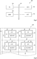
memory cell 300. This allows for a high-density storage of information in memory devices (not shown) comprising a plurality ofPCM cells 300, where two bits of data can be stored in eachPCM cell 300. -
Figure 5 schematically shows an embodiment of amemory 500. - The
memory 500 comprises: - one or a plurality of memory devices, such as devices comprising
memory cells 200 and/or 300 previously described in relation withFigures 3 and4 , and shown inFigure 5 by a block 502 (NVM); - a data processing unit, represented by a block 504 (PU), for example, a microprocessor;
- one or a plurality of memory devices, represented by a block 506 (MEM), and which may be memory devices different from those of
block 502; - a block 508 (FCT) comprising other electronic functions, for example, sensors, load control circuits, etc.; and
- a
data bus 510 enabling to transfer data between the different components. - The
block 502 preferably includes a circuit for addressing the array ofmemory cells 200 and/or 300. - It is possible, for the memory devices of the
block 506, not to be phase-change memory devices but to be RAMs, reprogrammable volatile memories (EEPROM, flash, etc.). - As an alternative, the
block 506 may be omitted. The memory devices of thememory 500 are then only memory devices such as memory devices comprisingmemory cells 200 and/or 300. The memory is then entirely a non-volatile memory. -
Figure 6 schematically shows an embodiment of aneuromorphic chip 600. - The
neuromorphic chip 600 comprises an array ofneuron cores 60 forming a distributed, parallel architecture. These neuron cores are linked, preferably coupled together, by one orseveral buses 62. The bus orbuses 62 are a functional equivalent of synapses inside a brain or neural network. - Each
neuron core 60 comprises: - an input/output unit, represented by a block 64 (I/O), which is connected to the bus or
buses 62; - a central processing unit, represented by a block 66 (CPU), for example, a microprocessor; and
- a memory device, such as
memory 500 previously described in relation withFigure 5 , and shown inFigure 6 by a block 68 (MEMORY), or containing only part of the components ofmemory 500, at least amemory device 502 of phase-change memory cells as described in relation withFigures 3 and4 . - The use of a
memory device 68 comprising memory cells such asmemory cells neuron core 60. This results in a smallerneuromorphic chip 600 which can therefore be more easily implemented in a circuit. - Various embodiments and variants have been described. Those skilled in the art will understand that certain features of these embodiments can be combined and other variants will readily occur to those skilled in the art. In particular, although the methods of writing described in relation with
Figures 3 and4 yield a number of respectively three and four memory states, it should be understood that a higher number of memory states could further be achieved in both cases, provided that the change in electrical resistance between these memory states is significant enough to be reliably measured. - Finally, the practical implementation of the embodiments and variants described herein is within the capabilities of those skilled in the art based on the functional description provided hereinabove.
Claims (12)
- A phase-change memory cell (200; 300), comprising:a heater (202);a crystalline layer (206), located above said heater (202) and covered by a conductive layer (208); anda resistive layer (210), interposed between said heater (202) and said crystalline layer (206),all side walls of said crystalline layer being totally surrounded by an insulating region (212), wherein:a first memory state is defined by having an amorphous region (206A) totally covering a top surface (2100) of said resistive layer (210); andat least one further memory state is defined by having said amorphous region (206A) partially covering said top surface (2100) of said resistive layer (210).
- A method of writing into the cell of claim 1, wherein said cell (200; 300) is heated, by said heater (202), up to a temperature sufficient to partially or totally amorphize said crystalline layer (206).
- The cell of claim 1, or the method of claim 2, wherein an electrical resistance of said cell (200; 300) is changed by amorphizing said crystalline layer (206).
- The cell of claim 1 or 3, or the method of claim 2 or 3, wherein the electrical resistance of said cell (200; 300) increases monotonically by increasing a part of the amorphous region (206A) that covers the top surface (2100) of said resistive layer (210).
- The cell of claim 1, 3 or 4, or the method of any of claims 2 to 4, wherein a second memory state is defined by having no amorphous region (206A) covering said top surface (2100) of said resistive layer (210), said at least one further memory state corresponding to an intermediate memory state between said first memory state and said second memory state.
- The cell or the method of claim 5, wherein exactly one intermediate memory state is defined by having said amorphous region (206A) partially covering said top surface (2100) of said resistive layer (210).
- The cell or the method of claim 6, wherein said heater (202) is centred with respect to said cell (200).
- The cell or the method of claim 5, wherein exactly two intermediate memory states are defined by having said amorphous region (206A) partially covering said top surface (2100) of said resistive layer (210).
- The cell or the method of claim 8, wherein said heater (202) is offset from a center of said cell (300).
- The cell of any of claims 1, 3 to 9, or the method of any of claims 2 to 9, wherein said crystalline layer (206) is made of a chalcogenide alloy of germanium, of antimony, and of tellurium, GST.
- A memory device (500) comprising at least one memory cell (200; 300) of any of claims 1, 3 to 10.
- A neuromorphic chip (600) comprising at least one memory device (500) of claim 11.
Applications Claiming Priority (1)
| Application Number | Priority Date | Filing Date | Title |
|---|---|---|---|
| FR1905663A FR3096826B1 (en) | 2019-05-28 | 2019-05-28 | memory cell |
Publications (2)
| Publication Number | Publication Date |
|---|---|
| EP3745402A1 true EP3745402A1 (en) | 2020-12-02 |
| EP3745402B1 EP3745402B1 (en) | 2024-08-07 |
Family
ID=68987742
Family Applications (1)
| Application Number | Title | Priority Date | Filing Date |
|---|---|---|---|
| EP20177258.9A Active EP3745402B1 (en) | 2019-05-28 | 2020-05-28 | Memory cell |
Country Status (3)
| Country | Link |
|---|---|
| US (1) | US11227992B2 (en) |
| EP (1) | EP3745402B1 (en) |
| FR (1) | FR3096826B1 (en) |
Cited By (2)
| Publication number | Priority date | Publication date | Assignee | Title |
|---|---|---|---|---|
| IT202200001130A1 (en) * | 2022-01-24 | 2023-07-24 | St Microelectronics Srl | PHASE CHANGE MEMORY CELL WITH ASYMMETRIC STRUCTURE, MEMORY DEVICE INCLUDING THE PHASE CHANGE MEMORY CELL, AND METHOD FOR MANUFACTURING THE PHASE CHANGE MEMORY CELL |
| FR3155407A1 (en) * | 2023-11-09 | 2025-05-16 | Stmicroelectronics International N.V. | Electronic device |
Families Citing this family (8)
| Publication number | Priority date | Publication date | Assignee | Title |
|---|---|---|---|---|
| FR3107138B1 (en) | 2020-02-06 | 2022-02-11 | Commissariat Energie Atomique | Phase change memory cell |
| US11456415B2 (en) | 2020-12-08 | 2022-09-27 | International Business Machines Corporation | Phase change memory cell with a wrap around and ring type of electrode contact and a projection liner |
| US11476418B2 (en) | 2020-12-08 | 2022-10-18 | International Business Machines Corporation | Phase change memory cell with a projection liner |
| US12402546B2 (en) | 2021-12-28 | 2025-08-26 | International Business Machines Corporation | Composite material phase change memory cell |
| CN116490058A (en) * | 2022-01-24 | 2023-07-25 | 意法半导体股份有限公司 | Phase change memory cell, memory device, and corresponding method |
| US20240074336A1 (en) * | 2022-08-24 | 2024-02-29 | International Business Machines Corporation | Self-aligned patterned projection liner for sidewall electrode pcm |
| US20240130252A1 (en) * | 2022-10-17 | 2024-04-18 | Taiwan Semiconductor Manufacturing Company, Ltd. | Thermal barrier structure in phase change material device |
| US20250048940A1 (en) | 2023-08-01 | 2025-02-06 | Stmicroelectronics International N.V. | Process for cointegration of two phase change memory (pcm) arrays having different phase change materials, and in-memory computation system utilizing the two pcm arrays |
Citations (3)
| Publication number | Priority date | Publication date | Assignee | Title |
|---|---|---|---|---|
| WO2008068807A1 (en) * | 2006-11-30 | 2008-06-12 | Renesas Technology Corp. | Semiconductor device fabricating method and semiconductor device |
| US20090261313A1 (en) * | 2008-04-22 | 2009-10-22 | Macronix International Co., Ltd. | Memory cell having a buried phase change region and method for fabricating the same |
| EP2706582A1 (en) * | 2012-09-10 | 2014-03-12 | STMicroelectronics (Crolles 2) SAS | Phase-change memory cell |
Family Cites Families (1)
| Publication number | Priority date | Publication date | Assignee | Title |
|---|---|---|---|---|
| EP1677371A1 (en) * | 2004-12-30 | 2006-07-05 | STMicroelectronics S.r.l. | Dual resistance heater for phase change devices and manufacturing method thereof |
-
2019
- 2019-05-28 FR FR1905663A patent/FR3096826B1/en active Active
-
2020
- 2020-05-26 US US16/883,190 patent/US11227992B2/en active Active
- 2020-05-28 EP EP20177258.9A patent/EP3745402B1/en active Active
Patent Citations (3)
| Publication number | Priority date | Publication date | Assignee | Title |
|---|---|---|---|---|
| WO2008068807A1 (en) * | 2006-11-30 | 2008-06-12 | Renesas Technology Corp. | Semiconductor device fabricating method and semiconductor device |
| US20090261313A1 (en) * | 2008-04-22 | 2009-10-22 | Macronix International Co., Ltd. | Memory cell having a buried phase change region and method for fabricating the same |
| EP2706582A1 (en) * | 2012-09-10 | 2014-03-12 | STMicroelectronics (Crolles 2) SAS | Phase-change memory cell |
Cited By (4)
| Publication number | Priority date | Publication date | Assignee | Title |
|---|---|---|---|---|
| IT202200001130A1 (en) * | 2022-01-24 | 2023-07-24 | St Microelectronics Srl | PHASE CHANGE MEMORY CELL WITH ASYMMETRIC STRUCTURE, MEMORY DEVICE INCLUDING THE PHASE CHANGE MEMORY CELL, AND METHOD FOR MANUFACTURING THE PHASE CHANGE MEMORY CELL |
| EP4216698A1 (en) | 2022-01-24 | 2023-07-26 | STMicroelectronics S.r.l. | A phase-change memory cell with asymmetric structure, a memory device including the phase-change memory cell, and a method for manufacturing the phase-change memory cell |
| US12520738B2 (en) | 2022-01-24 | 2026-01-06 | Stmicroelectronics S.R.L. | Phase-change memory cell with asymmetric structure, a memory device including the phase-change memory cell, and a method for manufacturing the phase-change memory cell |
| FR3155407A1 (en) * | 2023-11-09 | 2025-05-16 | Stmicroelectronics International N.V. | Electronic device |
Also Published As
| Publication number | Publication date |
|---|---|
| US11227992B2 (en) | 2022-01-18 |
| FR3096826A1 (en) | 2020-12-04 |
| US20200381618A1 (en) | 2020-12-03 |
| FR3096826B1 (en) | 2022-06-03 |
| EP3745402B1 (en) | 2024-08-07 |
Similar Documents
| Publication | Publication Date | Title |
|---|---|---|
| EP3745402B1 (en) | Memory cell | |
| US10879459B2 (en) | Phase change memory cell with constriction structure | |
| US12114580B2 (en) | Phase-change memory cell | |
| US8373151B2 (en) | Write-once memory array including phase-change elements and threshold switch isolation | |
| US6579760B1 (en) | Self-aligned, programmable phase change memory | |
| US6894305B2 (en) | Phase-change memory devices with a self-heater structure | |
| EP1326254B1 (en) | Architecture of a phase-change nonvolatile memory array | |
| CN101872778B (en) | Integrated circuit 3D phase change memory array and manufacturing method | |
| EP2162887B1 (en) | Electric device comprising phase change material and heating element | |
| EP1811564B1 (en) | Electrical fuse device based on a phase-change memory element and corresponding programming method | |
| US20100163833A1 (en) | Electrical fuse device based on a phase-change memory element and corresponding programming method | |
| US20090065761A1 (en) | Programmable fuse/non-volatile memory structures in beol regions using externally heated phase change material | |
| CN111971808B (en) | Resistive 3D Memory | |
| US20080304311A1 (en) | Integrated circuit including logic portion and memory portion | |
| US12349370B2 (en) | Elementary cell comprising a resistive memory and a device intended to form a selector, cell matrix, associated manufacturing and initialization methods | |
| CN222941178U (en) | Phase change memory cell and memory device | |
| US20080273369A1 (en) | Integrated Circuit, Memory Module, Method of Operating an Integrated Circuit, and Computing System | |
| US7829877B2 (en) | Memory structure with a programmable resistive element and its manufacturing process | |
| KR20220133015A (en) | Resistive memory device | |
| US20240099168A1 (en) | Phase change memory cell | |
| CN217562572U (en) | Phase change memory | |
| US12520738B2 (en) | Phase-change memory cell with asymmetric structure, a memory device including the phase-change memory cell, and a method for manufacturing the phase-change memory cell | |
| CN106133841A (en) | Single programmable memory body, electronic system, operation single programmable memory body method and programming single programmable memory body method | |
| US20240099164A1 (en) | Phase change memory cell | |
| CN116490058A (en) | Phase change memory cell, memory device, and corresponding method |
Legal Events
| Date | Code | Title | Description |
|---|---|---|---|
| PUAI | Public reference made under article 153(3) epc to a published international application that has entered the european phase |
Free format text: ORIGINAL CODE: 0009012 |
|
| STAA | Information on the status of an ep patent application or granted ep patent |
Free format text: STATUS: REQUEST FOR EXAMINATION WAS MADE |
|
| 17P | Request for examination filed |
Effective date: 20200528 |
|
| AK | Designated contracting states |
Kind code of ref document: A1 Designated state(s): AL AT BE BG CH CY CZ DE DK EE ES FI FR GB GR HR HU IE IS IT LI LT LU LV MC MK MT NL NO PL PT RO RS SE SI SK SM TR |
|
| AX | Request for extension of the european patent |
Extension state: BA ME |
|
| STAA | Information on the status of an ep patent application or granted ep patent |
Free format text: STATUS: EXAMINATION IS IN PROGRESS |
|
| 17Q | First examination report despatched |
Effective date: 20220128 |
|
| GRAP | Despatch of communication of intention to grant a patent |
Free format text: ORIGINAL CODE: EPIDOSNIGR1 |
|
| STAA | Information on the status of an ep patent application or granted ep patent |
Free format text: STATUS: GRANT OF PATENT IS INTENDED |
|
| RIC1 | Information provided on ipc code assigned before grant |
Ipc: H10N 70/00 20230101ALI20240312BHEP Ipc: H10N 70/20 20230101ALI20240312BHEP Ipc: G11C 11/54 20060101ALI20240312BHEP Ipc: G11C 13/00 20060101ALI20240312BHEP Ipc: G11C 11/56 20060101AFI20240312BHEP |
|
| INTG | Intention to grant announced |
Effective date: 20240416 |
|
| RIN1 | Information on inventor provided before grant (corrected) |
Inventor name: CAPPELLETTI, PAOLO GIUSEPPE |
|
| GRAS | Grant fee paid |
Free format text: ORIGINAL CODE: EPIDOSNIGR3 |
|
| GRAA | (expected) grant |
Free format text: ORIGINAL CODE: 0009210 |
|
| STAA | Information on the status of an ep patent application or granted ep patent |
Free format text: STATUS: THE PATENT HAS BEEN GRANTED |
|
| AK | Designated contracting states |
Kind code of ref document: B1 Designated state(s): AL AT BE BG CH CY CZ DE DK EE ES FI FR GB GR HR HU IE IS IT LI LT LU LV MC MK MT NL NO PL PT RO RS SE SI SK SM TR |
|
| REG | Reference to a national code |
Ref country code: GB Ref legal event code: FG4D |
|
| REG | Reference to a national code |
Ref country code: CH Ref legal event code: EP |
|
| REG | Reference to a national code |
Ref country code: IE Ref legal event code: FG4D |
|
| REG | Reference to a national code |
Ref country code: DE Ref legal event code: R096 Ref document number: 602020035169 Country of ref document: DE |
|
| REG | Reference to a national code |
Ref country code: LT Ref legal event code: MG9D |
|
| REG | Reference to a national code |
Ref country code: NL Ref legal event code: MP Effective date: 20240807 |
|
| PG25 | Lapsed in a contracting state [announced via postgrant information from national office to epo] |
Ref country code: NO Free format text: LAPSE BECAUSE OF FAILURE TO SUBMIT A TRANSLATION OF THE DESCRIPTION OR TO PAY THE FEE WITHIN THE PRESCRIBED TIME-LIMIT Effective date: 20241107 |
|
| REG | Reference to a national code |
Ref country code: AT Ref legal event code: MK05 Ref document number: 1711882 Country of ref document: AT Kind code of ref document: T Effective date: 20240807 |
|
| PG25 | Lapsed in a contracting state [announced via postgrant information from national office to epo] |
Ref country code: NL Free format text: LAPSE BECAUSE OF FAILURE TO SUBMIT A TRANSLATION OF THE DESCRIPTION OR TO PAY THE FEE WITHIN THE PRESCRIBED TIME-LIMIT Effective date: 20240807 Ref country code: FI Free format text: LAPSE BECAUSE OF FAILURE TO SUBMIT A TRANSLATION OF THE DESCRIPTION OR TO PAY THE FEE WITHIN THE PRESCRIBED TIME-LIMIT Effective date: 20240807 Ref country code: PT Free format text: LAPSE BECAUSE OF FAILURE TO SUBMIT A TRANSLATION OF THE DESCRIPTION OR TO PAY THE FEE WITHIN THE PRESCRIBED TIME-LIMIT Effective date: 20241209 Ref country code: GR Free format text: LAPSE BECAUSE OF FAILURE TO SUBMIT A TRANSLATION OF THE DESCRIPTION OR TO PAY THE FEE WITHIN THE PRESCRIBED TIME-LIMIT Effective date: 20241108 Ref country code: PL Free format text: LAPSE BECAUSE OF FAILURE TO SUBMIT A TRANSLATION OF THE DESCRIPTION OR TO PAY THE FEE WITHIN THE PRESCRIBED TIME-LIMIT Effective date: 20240807 |
|
| PG25 | Lapsed in a contracting state [announced via postgrant information from national office to epo] |
Ref country code: BG Free format text: LAPSE BECAUSE OF FAILURE TO SUBMIT A TRANSLATION OF THE DESCRIPTION OR TO PAY THE FEE WITHIN THE PRESCRIBED TIME-LIMIT Effective date: 20240807 |
|
| PG25 | Lapsed in a contracting state [announced via postgrant information from national office to epo] |
Ref country code: LV Free format text: LAPSE BECAUSE OF FAILURE TO SUBMIT A TRANSLATION OF THE DESCRIPTION OR TO PAY THE FEE WITHIN THE PRESCRIBED TIME-LIMIT Effective date: 20240807 |
|
| PG25 | Lapsed in a contracting state [announced via postgrant information from national office to epo] |
Ref country code: AT Free format text: LAPSE BECAUSE OF FAILURE TO SUBMIT A TRANSLATION OF THE DESCRIPTION OR TO PAY THE FEE WITHIN THE PRESCRIBED TIME-LIMIT Effective date: 20240807 Ref country code: IS Free format text: LAPSE BECAUSE OF FAILURE TO SUBMIT A TRANSLATION OF THE DESCRIPTION OR TO PAY THE FEE WITHIN THE PRESCRIBED TIME-LIMIT Effective date: 20241207 |
|
| PG25 | Lapsed in a contracting state [announced via postgrant information from national office to epo] |
Ref country code: HR Free format text: LAPSE BECAUSE OF FAILURE TO SUBMIT A TRANSLATION OF THE DESCRIPTION OR TO PAY THE FEE WITHIN THE PRESCRIBED TIME-LIMIT Effective date: 20240807 |
|
| PG25 | Lapsed in a contracting state [announced via postgrant information from national office to epo] |
Ref country code: RS Free format text: LAPSE BECAUSE OF FAILURE TO SUBMIT A TRANSLATION OF THE DESCRIPTION OR TO PAY THE FEE WITHIN THE PRESCRIBED TIME-LIMIT Effective date: 20241107 Ref country code: ES Free format text: LAPSE BECAUSE OF FAILURE TO SUBMIT A TRANSLATION OF THE DESCRIPTION OR TO PAY THE FEE WITHIN THE PRESCRIBED TIME-LIMIT Effective date: 20240807 |
|
| PG25 | Lapsed in a contracting state [announced via postgrant information from national office to epo] |
Ref country code: RS Free format text: LAPSE BECAUSE OF FAILURE TO SUBMIT A TRANSLATION OF THE DESCRIPTION OR TO PAY THE FEE WITHIN THE PRESCRIBED TIME-LIMIT Effective date: 20241107 Ref country code: PT Free format text: LAPSE BECAUSE OF FAILURE TO SUBMIT A TRANSLATION OF THE DESCRIPTION OR TO PAY THE FEE WITHIN THE PRESCRIBED TIME-LIMIT Effective date: 20241209 Ref country code: PL Free format text: LAPSE BECAUSE OF FAILURE TO SUBMIT A TRANSLATION OF THE DESCRIPTION OR TO PAY THE FEE WITHIN THE PRESCRIBED TIME-LIMIT Effective date: 20240807 Ref country code: NO Free format text: LAPSE BECAUSE OF FAILURE TO SUBMIT A TRANSLATION OF THE DESCRIPTION OR TO PAY THE FEE WITHIN THE PRESCRIBED TIME-LIMIT Effective date: 20241107 Ref country code: NL Free format text: LAPSE BECAUSE OF FAILURE TO SUBMIT A TRANSLATION OF THE DESCRIPTION OR TO PAY THE FEE WITHIN THE PRESCRIBED TIME-LIMIT Effective date: 20240807 Ref country code: LV Free format text: LAPSE BECAUSE OF FAILURE TO SUBMIT A TRANSLATION OF THE DESCRIPTION OR TO PAY THE FEE WITHIN THE PRESCRIBED TIME-LIMIT Effective date: 20240807 Ref country code: IS Free format text: LAPSE BECAUSE OF FAILURE TO SUBMIT A TRANSLATION OF THE DESCRIPTION OR TO PAY THE FEE WITHIN THE PRESCRIBED TIME-LIMIT Effective date: 20241207 Ref country code: HR Free format text: LAPSE BECAUSE OF FAILURE TO SUBMIT A TRANSLATION OF THE DESCRIPTION OR TO PAY THE FEE WITHIN THE PRESCRIBED TIME-LIMIT Effective date: 20240807 Ref country code: GR Free format text: LAPSE BECAUSE OF FAILURE TO SUBMIT A TRANSLATION OF THE DESCRIPTION OR TO PAY THE FEE WITHIN THE PRESCRIBED TIME-LIMIT Effective date: 20241108 Ref country code: FI Free format text: LAPSE BECAUSE OF FAILURE TO SUBMIT A TRANSLATION OF THE DESCRIPTION OR TO PAY THE FEE WITHIN THE PRESCRIBED TIME-LIMIT Effective date: 20240807 Ref country code: ES Free format text: LAPSE BECAUSE OF FAILURE TO SUBMIT A TRANSLATION OF THE DESCRIPTION OR TO PAY THE FEE WITHIN THE PRESCRIBED TIME-LIMIT Effective date: 20240807 Ref country code: BG Free format text: LAPSE BECAUSE OF FAILURE TO SUBMIT A TRANSLATION OF THE DESCRIPTION OR TO PAY THE FEE WITHIN THE PRESCRIBED TIME-LIMIT Effective date: 20240807 Ref country code: AT Free format text: LAPSE BECAUSE OF FAILURE TO SUBMIT A TRANSLATION OF THE DESCRIPTION OR TO PAY THE FEE WITHIN THE PRESCRIBED TIME-LIMIT Effective date: 20240807 |
|
| PG25 | Lapsed in a contracting state [announced via postgrant information from national office to epo] |
Ref country code: DK Free format text: LAPSE BECAUSE OF FAILURE TO SUBMIT A TRANSLATION OF THE DESCRIPTION OR TO PAY THE FEE WITHIN THE PRESCRIBED TIME-LIMIT Effective date: 20240807 Ref country code: SM Free format text: LAPSE BECAUSE OF FAILURE TO SUBMIT A TRANSLATION OF THE DESCRIPTION OR TO PAY THE FEE WITHIN THE PRESCRIBED TIME-LIMIT Effective date: 20240807 |
|
| PG25 | Lapsed in a contracting state [announced via postgrant information from national office to epo] |
Ref country code: EE Free format text: LAPSE BECAUSE OF FAILURE TO SUBMIT A TRANSLATION OF THE DESCRIPTION OR TO PAY THE FEE WITHIN THE PRESCRIBED TIME-LIMIT Effective date: 20240807 |
|
| PG25 | Lapsed in a contracting state [announced via postgrant information from national office to epo] |
Ref country code: CZ Free format text: LAPSE BECAUSE OF FAILURE TO SUBMIT A TRANSLATION OF THE DESCRIPTION OR TO PAY THE FEE WITHIN THE PRESCRIBED TIME-LIMIT Effective date: 20240807 |
|
| PG25 | Lapsed in a contracting state [announced via postgrant information from national office to epo] |
Ref country code: SK Free format text: LAPSE BECAUSE OF FAILURE TO SUBMIT A TRANSLATION OF THE DESCRIPTION OR TO PAY THE FEE WITHIN THE PRESCRIBED TIME-LIMIT Effective date: 20240807 |
|
| REG | Reference to a national code |
Ref country code: DE Ref legal event code: R097 Ref document number: 602020035169 Country of ref document: DE |
|
| PLBE | No opposition filed within time limit |
Free format text: ORIGINAL CODE: 0009261 |
|
| STAA | Information on the status of an ep patent application or granted ep patent |
Free format text: STATUS: NO OPPOSITION FILED WITHIN TIME LIMIT |
|
| PGFP | Annual fee paid to national office [announced via postgrant information from national office to epo] |
Ref country code: DE Payment date: 20250423 Year of fee payment: 6 |
|
| 26N | No opposition filed |
Effective date: 20250508 |
|
| PG25 | Lapsed in a contracting state [announced via postgrant information from national office to epo] |
Ref country code: SE Free format text: LAPSE BECAUSE OF FAILURE TO SUBMIT A TRANSLATION OF THE DESCRIPTION OR TO PAY THE FEE WITHIN THE PRESCRIBED TIME-LIMIT Effective date: 20240807 |
|
| REG | Reference to a national code |
Ref country code: CH Ref legal event code: H13 Free format text: ST27 STATUS EVENT CODE: U-0-0-H10-H13 (AS PROVIDED BY THE NATIONAL OFFICE) Effective date: 20251223 |
|
| PG25 | Lapsed in a contracting state [announced via postgrant information from national office to epo] |
Ref country code: LU Free format text: LAPSE BECAUSE OF NON-PAYMENT OF DUE FEES Effective date: 20250528 |
|
| PG25 | Lapsed in a contracting state [announced via postgrant information from national office to epo] |
Ref country code: CH Free format text: LAPSE BECAUSE OF NON-PAYMENT OF DUE FEES Effective date: 20250531 |
|
| GBPC | Gb: european patent ceased through non-payment of renewal fee |
Effective date: 20250528 |
|
| PG25 | Lapsed in a contracting state [announced via postgrant information from national office to epo] |
Ref country code: IT Free format text: LAPSE BECAUSE OF FAILURE TO SUBMIT A TRANSLATION OF THE DESCRIPTION OR TO PAY THE FEE WITHIN THE PRESCRIBED TIME-LIMIT Effective date: 20240807 |
|
| REG | Reference to a national code |
Ref country code: BE Ref legal event code: MM Effective date: 20250531 |
|
| PG25 | Lapsed in a contracting state [announced via postgrant information from national office to epo] |
Ref country code: MC Free format text: LAPSE BECAUSE OF FAILURE TO SUBMIT A TRANSLATION OF THE DESCRIPTION OR TO PAY THE FEE WITHIN THE PRESCRIBED TIME-LIMIT Effective date: 20240807 |
|
| PG25 | Lapsed in a contracting state [announced via postgrant information from national office to epo] |
Ref country code: GB Free format text: LAPSE BECAUSE OF NON-PAYMENT OF DUE FEES Effective date: 20250528 |
|
| PG25 | Lapsed in a contracting state [announced via postgrant information from national office to epo] |
Ref country code: IE Free format text: LAPSE BECAUSE OF NON-PAYMENT OF DUE FEES Effective date: 20250528 |
|
| PG25 | Lapsed in a contracting state [announced via postgrant information from national office to epo] |
Ref country code: BE Free format text: LAPSE BECAUSE OF NON-PAYMENT OF DUE FEES Effective date: 20250531 |
|
| PG25 | Lapsed in a contracting state [announced via postgrant information from national office to epo] |
Ref country code: FR Free format text: LAPSE BECAUSE OF NON-PAYMENT OF DUE FEES Effective date: 20250531 |