EP4216263A1 - Memory device and method for forming same - Google Patents
Memory device and method for forming same Download PDFInfo
- Publication number
- EP4216263A1 EP4216263A1 EP22859776.1A EP22859776A EP4216263A1 EP 4216263 A1 EP4216263 A1 EP 4216263A1 EP 22859776 A EP22859776 A EP 22859776A EP 4216263 A1 EP4216263 A1 EP 4216263A1
- Authority
- EP
- European Patent Office
- Prior art keywords
- trench
- forming
- layer
- semiconductor substrate
- dielectric layer
- Prior art date
- Legal status (The legal status is an assumption and is not a legal conclusion. Google has not performed a legal analysis and makes no representation as to the accuracy of the status listed.)
- Pending
Links
- 238000000034 method Methods 0.000 title claims abstract description 85
- 239000000758 substrate Substances 0.000 claims abstract description 103
- 239000004065 semiconductor Substances 0.000 claims abstract description 102
- 229910052751 metal Inorganic materials 0.000 claims abstract description 59
- 239000002184 metal Substances 0.000 claims abstract description 59
- 239000003990 capacitor Substances 0.000 claims abstract description 42
- 239000000463 material Substances 0.000 claims description 74
- 230000008569 process Effects 0.000 claims description 59
- 239000012535 impurity Substances 0.000 claims description 57
- 150000002500 ions Chemical class 0.000 claims description 57
- 238000005530 etching Methods 0.000 claims description 42
- 230000015572 biosynthetic process Effects 0.000 claims description 23
- 238000005468 ion implantation Methods 0.000 claims description 19
- 230000000717 retained effect Effects 0.000 claims description 9
- 238000000059 patterning Methods 0.000 claims description 7
- 229910052782 aluminium Inorganic materials 0.000 claims description 5
- 229910052759 nickel Inorganic materials 0.000 claims description 5
- 229910052697 platinum Inorganic materials 0.000 claims description 5
- 229910052719 titanium Inorganic materials 0.000 claims description 5
- 229910052721 tungsten Inorganic materials 0.000 claims description 5
- 229910004166 TaN Inorganic materials 0.000 claims description 4
- 229910004200 TaSiN Inorganic materials 0.000 claims description 4
- ATJFFYVFTNAWJD-UHFFFAOYSA-N Tin Chemical compound [Sn] ATJFFYVFTNAWJD-UHFFFAOYSA-N 0.000 claims description 4
- 229910052802 copper Inorganic materials 0.000 claims description 4
- 229910052737 gold Inorganic materials 0.000 claims description 4
- 229910052709 silver Inorganic materials 0.000 claims description 4
- 229910052718 tin Inorganic materials 0.000 claims description 4
- 238000003860 storage Methods 0.000 abstract description 17
- 239000010410 layer Substances 0.000 description 246
- XUIMIQQOPSSXEZ-UHFFFAOYSA-N Silicon Chemical compound [Si] XUIMIQQOPSSXEZ-UHFFFAOYSA-N 0.000 description 31
- 229910052710 silicon Inorganic materials 0.000 description 31
- 239000010703 silicon Substances 0.000 description 31
- 229910052581 Si3N4 Inorganic materials 0.000 description 28
- HQVNEWCFYHHQES-UHFFFAOYSA-N silicon nitride Chemical compound N12[Si]34N5[Si]62N3[Si]51N64 HQVNEWCFYHHQES-UHFFFAOYSA-N 0.000 description 28
- HBMJWWWQQXIZIP-UHFFFAOYSA-N silicon carbide Chemical compound [Si+]#[C-] HBMJWWWQQXIZIP-UHFFFAOYSA-N 0.000 description 22
- 229910010271 silicon carbide Inorganic materials 0.000 description 21
- VYPSYNLAJGMNEJ-UHFFFAOYSA-N Silicium dioxide Chemical group O=[Si]=O VYPSYNLAJGMNEJ-UHFFFAOYSA-N 0.000 description 19
- 229910052814 silicon oxide Inorganic materials 0.000 description 18
- -1 boron ions Chemical class 0.000 description 16
- 229910021420 polycrystalline silicon Inorganic materials 0.000 description 11
- 238000010586 diagram Methods 0.000 description 10
- 229910000577 Silicon-germanium Inorganic materials 0.000 description 9
- LEVVHYCKPQWKOP-UHFFFAOYSA-N [Si].[Ge] Chemical compound [Si].[Ge] LEVVHYCKPQWKOP-UHFFFAOYSA-N 0.000 description 9
- 229910003481 amorphous carbon Inorganic materials 0.000 description 9
- 238000005520 cutting process Methods 0.000 description 9
- 230000015654 memory Effects 0.000 description 9
- 229910021417 amorphous silicon Inorganic materials 0.000 description 8
- 239000003989 dielectric material Substances 0.000 description 8
- 239000011241 protective layer Substances 0.000 description 8
- 238000000231 atomic layer deposition Methods 0.000 description 7
- 238000005137 deposition process Methods 0.000 description 7
- 238000001312 dry etching Methods 0.000 description 6
- 230000002349 favourable effect Effects 0.000 description 6
- PXHVJJICTQNCMI-UHFFFAOYSA-N nickel Substances [Ni] PXHVJJICTQNCMI-UHFFFAOYSA-N 0.000 description 5
- 238000005240 physical vapour deposition Methods 0.000 description 5
- 238000001020 plasma etching Methods 0.000 description 5
- 238000000623 plasma-assisted chemical vapour deposition Methods 0.000 description 5
- BASFCYQUMIYNBI-UHFFFAOYSA-N platinum Substances [Pt] BASFCYQUMIYNBI-UHFFFAOYSA-N 0.000 description 5
- 238000002230 thermal chemical vapour deposition Methods 0.000 description 5
- GWEVSGVZZGPLCZ-UHFFFAOYSA-N Titan oxide Chemical compound O=[Ti]=O GWEVSGVZZGPLCZ-UHFFFAOYSA-N 0.000 description 4
- MCMNRKCIXSYSNV-UHFFFAOYSA-N Zirconium dioxide Chemical compound O=[Zr]=O MCMNRKCIXSYSNV-UHFFFAOYSA-N 0.000 description 4
- 238000001505 atmospheric-pressure chemical vapour deposition Methods 0.000 description 4
- 230000000694 effects Effects 0.000 description 4
- 238000009713 electroplating Methods 0.000 description 4
- 238000004518 low pressure chemical vapour deposition Methods 0.000 description 4
- 238000001465 metallisation Methods 0.000 description 4
- 238000004528 spin coating Methods 0.000 description 4
- 238000004544 sputter deposition Methods 0.000 description 4
- 239000010936 titanium Substances 0.000 description 4
- 229910001439 antimony ion Inorganic materials 0.000 description 3
- 229910052785 arsenic Inorganic materials 0.000 description 3
- 229910052796 boron Inorganic materials 0.000 description 3
- 239000010949 copper Substances 0.000 description 3
- 229910052733 gallium Inorganic materials 0.000 description 3
- 239000010931 gold Substances 0.000 description 3
- 229910001449 indium ion Inorganic materials 0.000 description 3
- 230000003647 oxidation Effects 0.000 description 3
- 238000007254 oxidation reaction Methods 0.000 description 3
- 229910052698 phosphorus Inorganic materials 0.000 description 3
- 239000011574 phosphorus Substances 0.000 description 3
- 229920002120 photoresistant polymer Polymers 0.000 description 3
- 239000010944 silver (metal) Substances 0.000 description 3
- 239000011135 tin Substances 0.000 description 3
- 229910015801 BaSrTiO Inorganic materials 0.000 description 2
- NRTOMJZYCJJWKI-UHFFFAOYSA-N Titanium nitride Chemical compound [Ti]#N NRTOMJZYCJJWKI-UHFFFAOYSA-N 0.000 description 2
- 230000004075 alteration Effects 0.000 description 2
- PNEYBMLMFCGWSK-UHFFFAOYSA-N aluminium oxide Inorganic materials [O-2].[O-2].[O-2].[Al+3].[Al+3] PNEYBMLMFCGWSK-UHFFFAOYSA-N 0.000 description 2
- 150000001875 compounds Chemical class 0.000 description 2
- 229910052593 corundum Inorganic materials 0.000 description 2
- 229910052732 germanium Inorganic materials 0.000 description 2
- GNPVGFCGXDBREM-UHFFFAOYSA-N germanium atom Chemical compound [Ge] GNPVGFCGXDBREM-UHFFFAOYSA-N 0.000 description 2
- CJNBYAVZURUTKZ-UHFFFAOYSA-N hafnium(IV) oxide Inorganic materials O=[Hf]=O CJNBYAVZURUTKZ-UHFFFAOYSA-N 0.000 description 2
- 239000012212 insulator Substances 0.000 description 2
- 230000010354 integration Effects 0.000 description 2
- 238000004519 manufacturing process Methods 0.000 description 2
- 238000012986 modification Methods 0.000 description 2
- 230000004048 modification Effects 0.000 description 2
- 239000011368 organic material Substances 0.000 description 2
- 239000002356 single layer Substances 0.000 description 2
- PBCFLUZVCVVTBY-UHFFFAOYSA-N tantalum pentoxide Inorganic materials O=[Ta](=O)O[Ta](=O)=O PBCFLUZVCVVTBY-UHFFFAOYSA-N 0.000 description 2
- 229910001845 yogo sapphire Inorganic materials 0.000 description 2
- JBRZTFJDHDCESZ-UHFFFAOYSA-N AsGa Chemical compound [As]#[Ga] JBRZTFJDHDCESZ-UHFFFAOYSA-N 0.000 description 1
- 229910001218 Gallium arsenide Inorganic materials 0.000 description 1
- 229910002370 SrTiO3 Inorganic materials 0.000 description 1
- RTAQQCXQSZGOHL-UHFFFAOYSA-N Titanium Chemical compound [Ti] RTAQQCXQSZGOHL-UHFFFAOYSA-N 0.000 description 1
- UGACIEPFGXRWCH-UHFFFAOYSA-N [Si].[Ti] Chemical compound [Si].[Ti] UGACIEPFGXRWCH-UHFFFAOYSA-N 0.000 description 1
- 230000001154 acute effect Effects 0.000 description 1
- XAGFODPZIPBFFR-UHFFFAOYSA-N aluminium Chemical compound [Al] XAGFODPZIPBFFR-UHFFFAOYSA-N 0.000 description 1
- 238000005229 chemical vapour deposition Methods 0.000 description 1
- 238000002513 implantation Methods 0.000 description 1
- 230000006872 improvement Effects 0.000 description 1
- 238000002955 isolation Methods 0.000 description 1
- RUFLMLWJRZAWLJ-UHFFFAOYSA-N nickel silicide Chemical compound [Ni]=[Si]=[Ni] RUFLMLWJRZAWLJ-UHFFFAOYSA-N 0.000 description 1
- 229910021334 nickel silicide Inorganic materials 0.000 description 1
- 150000004767 nitrides Chemical class 0.000 description 1
- 238000011160 research Methods 0.000 description 1
- 229910021332 silicide Inorganic materials 0.000 description 1
- FVBUAEGBCNSCDD-UHFFFAOYSA-N silicide(4-) Chemical compound [Si-4] FVBUAEGBCNSCDD-UHFFFAOYSA-N 0.000 description 1
- 229910021341 titanium silicide Inorganic materials 0.000 description 1
- WFKWXMTUELFFGS-UHFFFAOYSA-N tungsten Chemical compound [W] WFKWXMTUELFFGS-UHFFFAOYSA-N 0.000 description 1
- 239000010937 tungsten Substances 0.000 description 1
Images


Classifications
-
- H—ELECTRICITY
- H10—SEMICONDUCTOR DEVICES; ELECTRIC SOLID-STATE DEVICES NOT OTHERWISE PROVIDED FOR
- H10B—ELECTRONIC MEMORY DEVICES
- H10B12/00—Dynamic random access memory [DRAM] devices
- H10B12/01—Manufacture or treatment
- H10B12/02—Manufacture or treatment for one transistor one-capacitor [1T-1C] memory cells
- H10B12/03—Making the capacitor or connections thereto
- H10B12/033—Making the capacitor or connections thereto the capacitor extending over the transistor
-
- H—ELECTRICITY
- H10—SEMICONDUCTOR DEVICES; ELECTRIC SOLID-STATE DEVICES NOT OTHERWISE PROVIDED FOR
- H10B—ELECTRONIC MEMORY DEVICES
- H10B12/00—Dynamic random access memory [DRAM] devices
- H10B12/30—DRAM devices comprising one-transistor - one-capacitor [1T-1C] memory cells
- H10B12/31—DRAM devices comprising one-transistor - one-capacitor [1T-1C] memory cells having a storage electrode stacked over the transistor
- H10B12/315—DRAM devices comprising one-transistor - one-capacitor [1T-1C] memory cells having a storage electrode stacked over the transistor with the capacitor higher than a bit line
-
- H—ELECTRICITY
- H01—ELECTRIC ELEMENTS
- H01L—SEMICONDUCTOR DEVICES NOT COVERED BY CLASS H10
- H01L21/00—Processes or apparatus adapted for the manufacture or treatment of semiconductor or solid state devices or of parts thereof
- H01L21/70—Manufacture or treatment of devices consisting of a plurality of solid state components formed in or on a common substrate or of parts thereof; Manufacture of integrated circuit devices or of parts thereof
- H01L21/77—Manufacture or treatment of devices consisting of a plurality of solid state components or integrated circuits formed in, or on, a common substrate
- H01L21/78—Manufacture or treatment of devices consisting of a plurality of solid state components or integrated circuits formed in, or on, a common substrate with subsequent division of the substrate into plural individual devices
- H01L21/82—Manufacture or treatment of devices consisting of a plurality of solid state components or integrated circuits formed in, or on, a common substrate with subsequent division of the substrate into plural individual devices to produce devices, e.g. integrated circuits, each consisting of a plurality of components
- H01L21/822—Manufacture or treatment of devices consisting of a plurality of solid state components or integrated circuits formed in, or on, a common substrate with subsequent division of the substrate into plural individual devices to produce devices, e.g. integrated circuits, each consisting of a plurality of components the substrate being a semiconductor, using silicon technology
- H01L21/8232—Field-effect technology
- H01L21/8234—MIS technology, i.e. integration processes of field effect transistors of the conductor-insulator-semiconductor type
- H01L21/823412—MIS technology, i.e. integration processes of field effect transistors of the conductor-insulator-semiconductor type with a particular manufacturing method of the channel structures, e.g. channel implants, halo or pocket implants, or channel materials
-
- H—ELECTRICITY
- H01—ELECTRIC ELEMENTS
- H01L—SEMICONDUCTOR DEVICES NOT COVERED BY CLASS H10
- H01L21/00—Processes or apparatus adapted for the manufacture or treatment of semiconductor or solid state devices or of parts thereof
- H01L21/70—Manufacture or treatment of devices consisting of a plurality of solid state components formed in or on a common substrate or of parts thereof; Manufacture of integrated circuit devices or of parts thereof
- H01L21/77—Manufacture or treatment of devices consisting of a plurality of solid state components or integrated circuits formed in, or on, a common substrate
- H01L21/78—Manufacture or treatment of devices consisting of a plurality of solid state components or integrated circuits formed in, or on, a common substrate with subsequent division of the substrate into plural individual devices
- H01L21/82—Manufacture or treatment of devices consisting of a plurality of solid state components or integrated circuits formed in, or on, a common substrate with subsequent division of the substrate into plural individual devices to produce devices, e.g. integrated circuits, each consisting of a plurality of components
- H01L21/822—Manufacture or treatment of devices consisting of a plurality of solid state components or integrated circuits formed in, or on, a common substrate with subsequent division of the substrate into plural individual devices to produce devices, e.g. integrated circuits, each consisting of a plurality of components the substrate being a semiconductor, using silicon technology
- H01L21/8232—Field-effect technology
- H01L21/8234—MIS technology, i.e. integration processes of field effect transistors of the conductor-insulator-semiconductor type
- H01L21/823418—MIS technology, i.e. integration processes of field effect transistors of the conductor-insulator-semiconductor type with a particular manufacturing method of the source or drain structures, e.g. specific source or drain implants or silicided source or drain structures or raised source or drain structures
-
- H—ELECTRICITY
- H01—ELECTRIC ELEMENTS
- H01L—SEMICONDUCTOR DEVICES NOT COVERED BY CLASS H10
- H01L29/00—Semiconductor devices adapted for rectifying, amplifying, oscillating or switching, or capacitors or resistors with at least one potential-jump barrier or surface barrier, e.g. PN junction depletion layer or carrier concentration layer; Details of semiconductor bodies or of electrodes thereof ; Multistep manufacturing processes therefor
- H01L29/40—Electrodes ; Multistep manufacturing processes therefor
- H01L29/41—Electrodes ; Multistep manufacturing processes therefor characterised by their shape, relative sizes or dispositions
- H01L29/423—Electrodes ; Multistep manufacturing processes therefor characterised by their shape, relative sizes or dispositions not carrying the current to be rectified, amplified or switched
- H01L29/42312—Gate electrodes for field effect devices
- H01L29/42316—Gate electrodes for field effect devices for field-effect transistors
- H01L29/4232—Gate electrodes for field effect devices for field-effect transistors with insulated gate
- H01L29/42356—Disposition, e.g. buried gate electrode
- H01L29/4236—Disposition, e.g. buried gate electrode within a trench, e.g. trench gate electrode, groove gate electrode
-
- H—ELECTRICITY
- H01—ELECTRIC ELEMENTS
- H01L—SEMICONDUCTOR DEVICES NOT COVERED BY CLASS H10
- H01L29/00—Semiconductor devices adapted for rectifying, amplifying, oscillating or switching, or capacitors or resistors with at least one potential-jump barrier or surface barrier, e.g. PN junction depletion layer or carrier concentration layer; Details of semiconductor bodies or of electrodes thereof ; Multistep manufacturing processes therefor
- H01L29/66—Types of semiconductor device ; Multistep manufacturing processes therefor
- H01L29/66007—Multistep manufacturing processes
- H01L29/66075—Multistep manufacturing processes of devices having semiconductor bodies comprising group 14 or group 13/15 materials
- H01L29/66227—Multistep manufacturing processes of devices having semiconductor bodies comprising group 14 or group 13/15 materials the devices being controllable only by the electric current supplied or the electric potential applied, to an electrode which does not carry the current to be rectified, amplified or switched, e.g. three-terminal devices
- H01L29/66409—Unipolar field-effect transistors
- H01L29/66477—Unipolar field-effect transistors with an insulated gate, i.e. MISFET
- H01L29/66742—Thin film unipolar transistors
-
- H—ELECTRICITY
- H01—ELECTRIC ELEMENTS
- H01L—SEMICONDUCTOR DEVICES NOT COVERED BY CLASS H10
- H01L29/00—Semiconductor devices adapted for rectifying, amplifying, oscillating or switching, or capacitors or resistors with at least one potential-jump barrier or surface barrier, e.g. PN junction depletion layer or carrier concentration layer; Details of semiconductor bodies or of electrodes thereof ; Multistep manufacturing processes therefor
- H01L29/66—Types of semiconductor device ; Multistep manufacturing processes therefor
- H01L29/68—Types of semiconductor device ; Multistep manufacturing processes therefor controllable by only the electric current supplied, or only the electric potential applied, to an electrode which does not carry the current to be rectified, amplified or switched
- H01L29/76—Unipolar devices, e.g. field effect transistors
- H01L29/772—Field effect transistors
- H01L29/78—Field effect transistors with field effect produced by an insulated gate
- H01L29/786—Thin film transistors, i.e. transistors with a channel being at least partly a thin film
- H01L29/78642—Vertical transistors
-
- H—ELECTRICITY
- H01—ELECTRIC ELEMENTS
- H01L—SEMICONDUCTOR DEVICES NOT COVERED BY CLASS H10
- H01L29/00—Semiconductor devices adapted for rectifying, amplifying, oscillating or switching, or capacitors or resistors with at least one potential-jump barrier or surface barrier, e.g. PN junction depletion layer or carrier concentration layer; Details of semiconductor bodies or of electrodes thereof ; Multistep manufacturing processes therefor
- H01L29/66—Types of semiconductor device ; Multistep manufacturing processes therefor
- H01L29/68—Types of semiconductor device ; Multistep manufacturing processes therefor controllable by only the electric current supplied, or only the electric potential applied, to an electrode which does not carry the current to be rectified, amplified or switched
- H01L29/76—Unipolar devices, e.g. field effect transistors
- H01L29/772—Field effect transistors
- H01L29/78—Field effect transistors with field effect produced by an insulated gate
- H01L29/786—Thin film transistors, i.e. transistors with a channel being at least partly a thin film
- H01L29/78696—Thin film transistors, i.e. transistors with a channel being at least partly a thin film characterised by the structure of the channel, e.g. multichannel, transverse or longitudinal shape, length or width, doping structure, or the overlap or alignment between the channel and the gate, the source or the drain, or the contacting structure of the channel
-
- H—ELECTRICITY
- H10—SEMICONDUCTOR DEVICES; ELECTRIC SOLID-STATE DEVICES NOT OTHERWISE PROVIDED FOR
- H10B—ELECTRONIC MEMORY DEVICES
- H10B12/00—Dynamic random access memory [DRAM] devices
- H10B12/01—Manufacture or treatment
- H10B12/02—Manufacture or treatment for one transistor one-capacitor [1T-1C] memory cells
- H10B12/03—Making the capacitor or connections thereto
- H10B12/033—Making the capacitor or connections thereto the capacitor extending over the transistor
- H10B12/0335—Making a connection between the transistor and the capacitor, e.g. plug
-
- H—ELECTRICITY
- H10—SEMICONDUCTOR DEVICES; ELECTRIC SOLID-STATE DEVICES NOT OTHERWISE PROVIDED FOR
- H10B—ELECTRONIC MEMORY DEVICES
- H10B12/00—Dynamic random access memory [DRAM] devices
- H10B12/01—Manufacture or treatment
- H10B12/02—Manufacture or treatment for one transistor one-capacitor [1T-1C] memory cells
- H10B12/05—Making the transistor
- H10B12/053—Making the transistor the transistor being at least partially in a trench in the substrate
-
- H—ELECTRICITY
- H10—SEMICONDUCTOR DEVICES; ELECTRIC SOLID-STATE DEVICES NOT OTHERWISE PROVIDED FOR
- H10B—ELECTRONIC MEMORY DEVICES
- H10B12/00—Dynamic random access memory [DRAM] devices
- H10B12/30—DRAM devices comprising one-transistor - one-capacitor [1T-1C] memory cells
- H10B12/34—DRAM devices comprising one-transistor - one-capacitor [1T-1C] memory cells the transistor being at least partially in a trench in the substrate
-
- H—ELECTRICITY
- H10—SEMICONDUCTOR DEVICES; ELECTRIC SOLID-STATE DEVICES NOT OTHERWISE PROVIDED FOR
- H10B—ELECTRONIC MEMORY DEVICES
- H10B12/00—Dynamic random access memory [DRAM] devices
- H10B12/30—DRAM devices comprising one-transistor - one-capacitor [1T-1C] memory cells
- H10B12/48—Data lines or contacts therefor
- H10B12/482—Bit lines
-
- H—ELECTRICITY
- H10—SEMICONDUCTOR DEVICES; ELECTRIC SOLID-STATE DEVICES NOT OTHERWISE PROVIDED FOR
- H10B—ELECTRONIC MEMORY DEVICES
- H10B12/00—Dynamic random access memory [DRAM] devices
- H10B12/30—DRAM devices comprising one-transistor - one-capacitor [1T-1C] memory cells
- H10B12/48—Data lines or contacts therefor
- H10B12/485—Bit line contacts
Definitions
- the present application relates to the field of memories, and in particular, to a memory device and a forming method thereof.
- a dynamic random access memory is composed of many repeated memory cells.
- Each memory cell usually includes a capacitor and a transistor.
- a gate is connected to a word line (WL)
- a drain is connected to a bit line (BL)
- a source is connected to the capacitor.
- a voltage signal on the WL can control the transistor to turn on or off, and then data information stored in the capacitor is read through the BL, or data information is written into the capacitor through the BL for storage.
- the transistor in the existing DRAM usually uses a trench-type transistor structure.
- a line width of a transistor structure of the existing trench-type has been minimized and a storage capacity of the DRAM cannot be further improved. Therefore, how to further improve the storage capacity and storage density of the DRAM is an urgent problem to be resolved by those skilled in the art.
- the present application provides a novel memory device and a forming method thereof, which can further improve a storage capacity and storage density of the memory device.
- some embodiments of the present application provide a method of forming a memory device, including: providing a semiconductor substrate, wherein multiple active regions are formed in the semiconductor substrate, the multiple active regions are separated by multiple first trenches extending along a first direction and multiple second trenches extending along a second direction, and the first trench communicates with the corresponding second trench; forming, in the semiconductor substrate at a bottom of the first trench, a third trench extending along the first direction, wherein a width of the third trench is less than a width of the bottom of the first trench; forming a bit line doped region in the semiconductor substrate on two sides of the third trench and at the bottom of the first trench through an ion implantation process; forming a gate dielectric layer on a sidewall surface and a bottom surface of the first trench and a sidewall surface and a bottom surface of the second trench; forming a first dielectric layer that fills the third trench; forming a metal gate in the second trench and the first trench on the first dielectric layer, wherein a top surface
- the multiple active regions are arranged in rows and columns.
- a formation process of the multiple active regions includes: forming, on the semiconductor substrate, multiple first mask patterns extending along the first direction and parallel to each other, with a first opening formed between adjacent first mask patterns; forming, on the first mask patterns, multiple second mask patterns extending along the second direction and parallel to each other, with a second opening formed between adjacent second mask patterns; etching the first mask pattern along the second opening by using the second mask pattern as a mask, and segmenting the first mask pattern along the second direction, and forming multiple discrete block mask patterns; and etching the semiconductor substrate by using each of the block mask patterns as a mask, and forming, in the semiconductor substrate, the first trench corresponding to the first opening and the second trench corresponding to the second opening, wherein the retained semiconductor substrate between the first trench and the second trench is the multiple active regions.
- the first mask pattern and the second mask pattern are formed by using a self-aligned double patterning process.
- a formation process of the first mask pattern includes: forming a first hard mask layer on the semiconductor substrate; forming, on the first hard mask layer, multiple first strip structures extending along the first direction and arranged parallel to each other; forming a first sacrificial sidewall layer on a sidewall and a top surface of the first strip structure and on the first hard mask layer between the first strip structures; filling each portion between the first strip structures with a first filling layer; removing the first sacrificial sidewall layer on the sidewall surface of the first strip structure, and forming a third opening between the first strip structure and the first filling layer; and etching the first hard mask layer along the third opening, and forming the first opening in the first hard mask layer, and using the retained portion of the first hard mask layer as the first mask pattern.
- a formation process of the second mask pattern includes: forming a second hard mask layer on the semiconductor substrate and the first mask pattern; forming, on the second hard mask layer, multiple second strip structures arranged in parallel along the second direction; forming a second sacrificial sidewall layer on a sidewall and a top surface of the second strip structure and on a surface of the second hard mask layer between the second strip structures; filling each portion between the second strip structures with a second filling layer; removing the second sacrificial sidewall layer on the sidewall surface of the second strip structure, and forming a fourth opening between the second strip structure and a second filling layer; and etching the second hard mask layer along the fourth opening, and forming the second opening in the second hard mask layer, and using the retained portion of the second hard mask layer as the second mask pattern.
- the width of the third trench is 1/4 to 3/4 of the width of the bottom of the first trench.
- a formation process of the third trench includes: forming a third mask layer in the first trench, with a sixth opening formed in the third mask layer, extending along the first direction, and exposing a surface of a portion of the semiconductor substrate at the bottom of the first trench; and etching the semiconductor substrate along the sixth opening, and forming the third trench.
- the process of forming a bit line doped region in the semiconductor substrate on two sides of the third trench and at the bottom of the first trench through an ion implantation process includes: forming a fourth mask layer in the third trench and on the top surface of the active region, with a seventh opening formed in the fourth mask layer, extending along the first direction, and exposing the semiconductor substrate on the two sides of the third trench; and performing first ion implantation on the semiconductor substrate at the bottom of the seventh opening along the seventh opening, and forming the bit line doped regions in the semiconductor substrate on the two sides of the third trench and at the bottom of the first trench.
- impurity ions implanted through the first ion implantation are N-type impurity ions or P-type impurity ions, and the first ion implantation has energy of 20 kev to 100 kev, a dose of 1E13 to 1E22 atom/cm 2 , and an angle of 0 to 20 degrees.
- the source region is formed through second ion implantation, and a type of impurity ions implanted in the source region is the same as a type of impurity ions implanted in the bit line doped region.
- the process of forming, on a surface of the semiconductor substrate, a capacitor connected to the source region includes: forming a third dielectric layer on the active region and the second dielectric layer; forming, in the third dielectric layer, a through hole exposing a surface of the source region; forming a contact plug in the through hole; forming a fourth dielectric layer on the third dielectric layer; forming, in the fourth dielectric layer, a capacitor hole exposing the contact plug; and forming the capacitor in the capacitor hole.
- doping is performed in a well region on the semiconductor substrate, and a type of impurity ions doped in the well region is opposite to a type of impurity ions doped in the source region and a type of impurity ions doped in the bit line doped region.
- Some other embodiments of the present invention further provide a memory device, including: a semiconductor substrate, wherein multiple active regions are formed in the semiconductor substrate, the multiple active regions are separated by multiple first trenches extending along a first direction and multiple second trenches extending along a second direction, and the first trench communicates with the corresponding second trench; a third trench, extending along the first direction and located in the semiconductor substrate at a bottom of the first trench, wherein a width of the third trench is less than a width of the bottom of the first trench; a bit line doped region, located in the semiconductor substrate on two sides of the third trench and at the bottom of the first trench; a gate dielectric layer, located on a sidewall surface of the first trench and the second trench; a first dielectric layer that fills the third trench; a metal gate, located in the second trench and the first trench on the first dielectric layer, wherein a top surface of the metal gate is lower than a top surface of the active region, and the metal gate in the second trench is segmented along the second direction;
- the multiple active regions are arranged in rows and columns.
- the width of the third trench is 1/4 to 3/4 of the width of the bottom of the first trench.
- impurity ions doped in the bit line doped region are N-type impurity ions or P-type impurity ions.
- a type of impurity ions doped in the source region is the same as a type of the impurity ions doped in the bit line doped region.
- the memory device further includes: a third dielectric layer, located on the active region and the second dielectric layer, wherein a contact plug connected to the source region is formed in the third dielectric layer; and a fourth dielectric layer located on the third dielectric layer, wherein a capacitor hole exposing the contact plug is formed in the fourth dielectric layer, and the capacitor is located in the capacitor hole.
- a material of the metal gate is one or more of W, Al, Cu, Ag, Au, Pt, Ni, Ti, TiN, TaN, Ta, TaC, TaSiN, WN, and Wsi.
- multiple active regions are formed in the semiconductor substrate, and after the multiple active regions are separated by multiple first trenches extending along a first direction and multiple second trenches extending along a second direction, a third trench extending along the first direction is formed in a portion of the semiconductor substrate at the bottom of each of the first trenches, where a width of the third trench is less than a width of the bottom of the first trench; bit line doped regions are formed in portions of the semiconductor substrate on two sides of the third trench and at the bottom of the first trench through an ion implantation process; a gate dielectric layer is formed on sidewall surfaces and a bottom surface of each of the first trench and the second trench; a first dielectric layer that fills the third trench is formed; a metal gate is formed in each of the first trench on the first dielectric layer and the second trench, where a top surface of the metal gate is lower than a top surface of the active region; a portion of each of the first trench
- each vertical transistor includes a corresponding active region, a gate dielectric layer located on a sidewall surface of the active region, bit line doped regions located in portions of a semiconductor substrate at the bottom of a first trench and on two sides of a third trench, a source region located on a top surface of the active region, and a metal gate located in each of the first trench and a second trench and surrounding the active region.
- a source region and a drain region are located on an upper side and a lower side of the active region, and a formed channel region is located on a sidewall of the active region, such that an area of the semiconductor substrate occupied by the vertical transistor is relatively small, a quantity of vertical transistors formed per unit area can be increased, and correspondingly, a quantity of capacitors connected to the source region of each transistor and subsequently formed per unit area can also be increased, thereby improving a storage capacity and storage density of a memory.
- use of the vertical transistor of such a specific structure can reduce a body effect, reduce a leakage current generated by a subsequently formed capacitor into the substrate, and improve electrical properties of the memory device.
- FIG. 1 to FIG. 39 are each a schematic structural diagram of a formation process of a memory device according to an embodiment of the present application.
- a trench-type transistor usually includes at least one buried word line located in a semiconductor substrate and one drain region and at least one source region located in portions of the semiconductor substrate on two sides of the buried word line.
- Such a trench-type transistor occupies a relatively large area of the semiconductor substrate, which is not conducive to improvement of integration of the DRAM, thus limiting the storage capacity and storage density of the DRAM.
- the present application provides a novel memory device and a forming method thereof, which can further improve a storage capacity and storage density of the memory device.
- FIG. 13 is a schematic structural diagram of a cross section of FIG. 15 along a direction of a cutting line AB
- FIG. 14 is a schematic structural diagram of a cross section of FIG. 15 along a direction of a cutting line CD
- a semiconductor substrate 201 is provided.
- Multiple active regions 213 are formed in the semiconductor substrate 201, and the multiple active regions 213 are separated by multiple first trenches 214 extending along a first direction and multiple second trenches 215 extending along a second direction.
- the first trench 214 communicates with the corresponding second trench 215.
- a material of the semiconductor substrate 201 may be silicon (Si), germanium (Ge), silicon-germanium (GeSi), or silicon carbide (SiC); or may be silicon on insulator (SOI) or germanium on insulator (GOI); or may be another material such as gallium arsenide or other III-V compounds.
- the material of the semiconductor substrate 201 is silicon.
- the semiconductor substrate 201 needs to be doped with some impurity ions according to a type of a subsequently formed vertical transistor. For example, doping may be performed in a well region on the semiconductor substrate.
- the impurity ions may be N-type impurity ions or P-type impurity ions.
- the P-type impurity ions are one or more of boron ions, gallium ions, or indium ions.
- the N-type impurity ions are one or more of phosphorus ions, arsenic ions, or antimony ions.
- the active region 213 is subsequently used to form a channel region of the vertical transistor.
- the multiple active regions 213 are discrete, and adjacent active regions 213 separated by cross-distributed first trenches 214 and second trenches 215.
- the formed active regions 213 are arranged in rows and columns (referring to FIG. 15 ). In other embodiments, the active regions may be arranged in another manner.
- first direction and the second direction are perpendicular to each other and have an angle of 90 degrees. In other embodiments, the first direction and the second direction may not be perpendicular to each other. For example, an angle between the first direction and the second direction may be an acute angle.
- the semiconductor substrate 201 may be first etched to form multiple first trenches 214, and then the semiconductor substrate 201 is etched to form multiple second trenches 215, thereby forming multiple discrete active regions 213.
- the first trench 214 and the second trench 215 may be formed simultaneously by etching the semiconductor substrate 201.
- the multiple active regions 213 are formed by using a self-aligned double patterning mask process.
- a formation process of the active region 213 is described in detail below with reference to FIG. 1 to FIG. 15 .
- a first hard mask layer 202 is formed on the semiconductor substrate 201; and a first material layer 203 is formed on the first hard mask layer 202.
- the first hard mask layer 202 is subsequently used to form a first mask pattern.
- the first hard mask layer 202 may be of a single-layer structure or a multi-layer stacked structure.
- a material of the first hard mask layer 202 may be one or more of polycrystalline silicon, amorphous silicon, amorphous carbon, silicon nitride, silicon oxynitride, silicon oxide, silicon nitride bonded silicon carbide, silicon oxycarbide, silicon carbide, and silicon-germanium.
- a process of forming the first hard mask layer 202 may be atmospheric or low pressure chemical vapor deposition (CVD), plasma enhanced chemical vapor deposition (PECVD), thermal chemical vapor deposition (Thermal CVD), physical vapor deposition (PVD), atomic layer deposition (ALD), sputtering, metallization, electroplating, spin coating, other suitable methods, and/or a combination thereof.
- CVD chemical vapor deposition
- PECVD plasma enhanced chemical vapor deposition
- Thermal CVD thermal chemical vapor deposition
- PVD physical vapor deposition
- ALD atomic layer deposition
- sputtering metallization
- electroplating electroplating
- spin coating other suitable methods, and/or a combination thereof.
- the material of the first hard mask layer 202 is polycrystalline silicon.
- a first etching stop layer may further be formed between the first hard mask layer 202 and the semiconductor substrate 201.
- the first etching stop layer is used to protect an underlying material layer from being over-etched during patterning of the first hard mask layer.
- a material of the first etching stop layer is different from that of the first hard mask layer.
- the material of the first etching stop layer is one or more of silicon nitride, silicon oxynitride, silicon oxide, silicon nitride bonded silicon carbide, and silicon oxycarbide. In this embodiment, the material of the first etching stop layer is silicon oxide.
- the first material layer 203 is subsequently used to form a first strip structure.
- the first material layer 203 may be of a single-layer structure or a multi-layer stacked structure.
- a material of the first material layer 203 may be one or more of polycrystalline silicon, amorphous silicon, amorphous carbon, silicon nitride, silicon oxynitride, silicon oxide, silicon nitride bonded silicon carbide, silicon oxycarbide, silicon carbide, and silicon-germanium.
- the material of the first material layer 203 is amorphous carbon.
- a second etching stop layer may further be formed between the first material layer 203 and the first hard mask layer 202.
- the second etching stop layer is used to protect an underlying material layer from being over-etched during patterning of the first material layer 203.
- a material of the second etching stop layer is different from that of the first material layer 203.
- the material of the second etching stop layer is one or more of silicon nitride, silicon oxynitride, silicon oxide, silicon nitride bonded silicon carbide, and silicon oxycarbide. In this embodiment, the material of the second etching stop layer is silicon oxynitride.
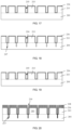
- FIG. 2 is a schematic structural diagram of a cross section of FIG. 3 along a direction of a cutting line AB.
- the first material layer 203 (referring to FIG. 1 ) is patterned.
- Multiple first strip structures 204 extending along the first direction and arranged parallel to each other are formed on the first hard mask layer.
- the first strip structure 204 is elongated.
- the multiple first strip structures 204 are discrete and parallel to each other.
- a fourth opening 205 is formed between adjacent first strip structures 204.
- the first material layer 203 is patterned by using an anisotropic dry etching process, and specifically, an anisotropic plasma etching process may be used.
- a patterned photoresist layer (not shown in the figure) may further be formed on the first material layer 203, and the first material layer 203 is etched by using the patterned photoresist layer as a mask to form a first strip structure 204; and the patterned photoresist layer is removed.
- FIG. 4 is performed on the basis of FIG. 2 , and a first sacrificial sidewall layer 206 is formed on sidewall and top surfaces of the first strip structure 204 and on a portion of the first hard mask layer 202 between first strip structures 204.
- a material of the first sacrificial sidewall layer 206 is different from that of the first strip structure.
- the material of the first sacrificial sidewall layer 206 may be one or more of polycrystalline silicon, amorphous silicon, amorphous carbon, silicon nitride, silicon oxynitride, silicon oxide, silicon nitride bonded silicon carbide, silicon oxycarbide, silicon carbide, and silicon-germanium.
- the first sacrificial sidewall layer 206 is formed by using a deposition process.
- the deposition process includes an atomic layer deposition process.
- each portion between the first strip structures 204 is filled with a first filling layer 207, and the first filling layer 207 fills the remaining portion of the fourth opening.
- a third opening is formed between the first strip structure 204 and the first filling layer 207 by removing portions of the first sacrificial sidewall layer on the sidewall surfaces of the first strip structure 204.
- a material of the first filling layer 207 is different from that of the first sacrificial sidewall layer 206.
- the material of the first filling layer 207 may be one or more of polycrystalline silicon, amorphous silicon, amorphous carbon, silicon nitride, silicon oxynitride, silicon oxide, silicon nitride bonded silicon carbide, silicon oxycarbide, silicon carbide, silicon-germanium, and an organic material.
- a process of forming the first filling layer 207 may be atmospheric or low pressure CVD, PECVD, thermal CVD, PVD, ALD, sputtering, metallization, electroplating, spin coating, other suitable methods, and/or a combination thereof.
- a surface of the formed first filling layer 207 may be flush with the first sacrificial sidewall layer 206 on the top surface of the first strip structure 204. Specifically, after a first filling material layer covering the first sacrificial sidewall layer 206 and filling the remaining portion of the fourth opening is formed, a portion of the first filling layer above the first sacrificial sidewall layer 206 on the top surface of the first strip structure 204 is removed by using a chemical-mechanical mask process. The remaining portion of the first filling material layer in the fourth opening is used as the first filling layer 207.
- a surface of the formed first filling layer may be flush with the top surface of the first strip structure 204.
- a portion of the first sacrificial sidewall layer 206 and the first filling material layer above the top surface of the first strip structure 204 are removed by using a chemical-mechanical mask process, to expose the top surface of the first strip structure 204, and the remaining portion of the first filling material layer in the fourth opening is used as the first filling layer. Therefore, a top surface of the formed first filling layer is flush with the top surface of the first strip structure.
- an etching load effect caused by a height difference between the filling layer and the first strip structure can be alleviated, accuracy of positions and sizes of the formed first mask patterns can be improved, and a favorable sidewall shape can be maintained, such that positions and sizes of block mask patterns formed after the first mask patterns are segmented have relatively high accuracy and a favorable sidewall shape is maintained, and finally, positions and sizes of active regions formed by etching the semiconductor substrate by using each of the block mask patterns as a mask have relatively high accuracy and a favorable sidewall shape is maintained.
- portions of the first sacrificial sidewall layer on the sidewall surfaces of the first strip structure 204 are removed, to form a third opening 208 between the first strip structure 204 and the first filling layer 207.
- the portions of the first sacrificial sidewall layer on the sidewall surfaces of the first strip structure 204 are removed by using an anisotropic dry etching process, including an anisotropic plasma etching process.
- the portion of the first sacrificial sidewall layer on the top surface of the first strip structure 204 is also removed.
- FIG. 7 is performed on the basis of FIG. 6
- FIG. 7 is a schematic structural diagram of a cross section of FIG. 9 along a direction of a cutting line AB
- FIG. 8 is a schematic structural diagram of a cross section of FIG. 9 along a direction of a cutting line CD.
- the first hard mask layer 202 (referring to FIG. 6 ) is etched along the third opening 208 (referring to FIG. 6 ), to form the first opening 210 in the first hard mask layer, and the retained portion of the first hard mask layer is used as the first mask pattern 209.
- the first hard mask layer 202 is etched by using an anisotropic dry etching process, including an anisotropic plasma etching process.
- the formed multiple first mask patterns 209 are discrete. Specifically, the formed first mask patterns 209 extend along the first direction and are parallel to each other, and a first opening 210 is formed between adjacent first mask patterns 209.
- the foregoing first mask pattern 209 is formed by using the foregoing self-aligned double patterning process, and subsequently, during the formation of the active region, a width of the first trench between active regions can be made relatively small, thereby allowing an area of the active region to be relatively large.
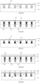
- FIG. 10 is a schematic structural diagram of a cross section of FIG. 12 along a direction of a cutting line AB
- FIG. 11 is a schematic structural diagram of a cross section of FIG. 12 along a direction of a cutting line CD.
- the first mask patterns 209 (referring to FIG. 7 to FIG. 9 ) are segmented along the second direction to form multiple discrete block mask patterns 211.
- the first mask patterns 209 are segmented along the second direction by using an anisotropic dry etching process.
- multiple second mask patterns extending along the second direction and parallel to each other are formed on the first mask pattern 209 and are each used as a mask for etching the first mask patterns 209, and a second opening is formed between adjacent second mask patterns; the first mask patterns 209 are etched along the second opening by using each of the second mask patterns as a mask, to segment the first mask patterns along the second direction to form multiple discrete block mask patterns 211; and the second mask patterns are removed.
- the second mask pattern may be formed by using a self-aligned double patterning process.
- a specific process includes: A formation process of the second mask pattern includes: forming a second hard mask layer on the semiconductor substrate and the first mask pattern; forming, on the second hard mask layer, multiple second strip structures arranged in parallel along the second direction; form a second sacrificial sidewall layer on a sidewall and top surfaces of the second strip structure and on a surface of a portion of the second hard mask layer between second strip structures; filling each portion between the second strip structures with a second filling layer; removing portions of the second sacrificial sidewall layer on the sidewall surfaces of the second strip structure, to form a fourth opening between the second strip structure and a second filling layer; and etching the second hard mask layer along the fourth opening, to form the second opening in the second hard mask layer, and using the retained portion of the second hard mask layer as the second mask pattern.
- a material of the second hard mask layer may be one or more of polycrystalline silicon, amorphous silicon, amorphous carbon, silicon nitride, silicon oxynitride, silicon oxide, silicon nitride bonded silicon carbide, silicon oxycarbide, silicon carbide, and silicon-germanium.
- a process of forming the second hard mask layer may be atmospheric or low pressure CVD, PECVD, thermal CVD, PVD, ALD, sputtering, metallization, electroplating, spin coating, other suitable methods, and/or a combination thereof.
- a fourth etching stop layer may further be formed between the second hard mask layer and the first mask pattern 209.
- a material of the fourth etching stop layer is different from that of the second hard mask layer.
- the material of the fourth etching stop layer is one or more of silicon nitride, silicon oxynitride, silicon oxide, silicon nitride bonded silicon carbide, and silicon oxycarbide.
- a material of the second strip structure may be one or more of polycrystalline silicon, amorphous silicon, amorphous carbon, silicon nitride, silicon oxynitride, silicon oxide, silicon nitride bonded silicon carbide, silicon oxycarbide, silicon carbide, and silicon-germanium.
- the second strip structure may be formed by etching a second material layer located on the second hard mask layer.
- a fifth etching stop layer may be further formed between the second material layer and the second hard mask layer.
- a material of the fifth etching stop layer is different from that of the second material layer.
- the material of the fifth etching stop layer is one or more of silicon nitride, silicon oxynitride, silicon oxide, silicon nitride bonded silicon carbide, and silicon oxycarbide.
- a material of the second sacrificial sidewall layer is different from that of the second strip structure.
- the material of the second sacrificial sidewall layer may be one or more of polycrystalline silicon, amorphous silicon, amorphous carbon, silicon nitride, silicon oxynitride, silicon oxide, silicon nitride bonded silicon carbide, silicon oxycarbide, silicon carbide, and silicon-germanium.
- the second sacrificial sidewall layer is formed by using a deposition process.
- the deposition process includes an atomic layer deposition process.
- a material of the second filling layer is different from that of the second sacrificial sidewall layer.
- the material of the second filling layer may be one or more of polycrystalline silicon, amorphous silicon, amorphous carbon, silicon nitride, silicon oxynitride, silicon oxide, silicon nitride bonded silicon carbide, silicon oxycarbide, silicon carbide, silicon-germanium, and an organic material.
- a process of forming the second filling layer may be atmospheric or low pressure CVD, PECVD, thermal CVD, PVD, ALD, sputtering, metallization, electroplating, spin coating, other suitable methods, and/or a combination thereof.
- a surface of the formed second filling layer may be flush with the second sacrificial sidewall layer on the top surface of the second strip structure.
- a portion of the second filling layer above the surface of the second sacrificial sidewall layer on the top surface of the second strip structure is removed by using a chemical-mechanical mask process. The remaining portion of the second filling material layer between the second strip structures is used as the second filling layer.
- a surface of the formed second filling layer may be flush with the top surface of the second strip structure.
- a portion of the second sacrificial sidewall layer and the second filling material layer above the top surface of the second strip structure are removed by using a chemical-mechanical mask process, to expose the top surface of the second strip structure, and the remaining portion of the second filling material layer in the space between the second strip structures is used as the second filling layer. Therefore, a top surface of the formed second filling layer is flush with the top surface of the second strip structure.
- an etching load effect caused by a height difference between the filling layer and the second strip structure can be alleviated, accuracy of positions and sizes of the formed second mask patterns can be improved, and a favorable sidewall shape can be maintained, such that positions and sizes of block mask patterns formed after the first mask patterns are segmented have relatively high accuracy and a favorable sidewall shape is maintained, and finally, positions and sizes of active regions formed by etching the semiconductor substrate by using each of the block mask patterns as a mask have relatively high accuracy and a favorable sidewall shape is maintained.
- the portions of the first sacrificial sidewall layer on the sidewall surfaces of the second strip structure are removed by using an anisotropic dry etching process, including an anisotropic plasma etching process.
- FIG. 13 is a schematic structural diagram of a cross section of FIG. 15 along a direction of a cutting line AB
- FIG. 14 is a schematic structural diagram of a cross section of FIG. 15 along a direction of a cutting line CD.
- the semiconductor substrate 201 is etched by using each of the block mask patterns (referring to FIG. 11 ) as a mask, to form, in the semiconductor substrate 201, first trenches 214 corresponding to the first openings and second trenches 215 corresponding to the second openings. Multiple first trenches 214 extend along the first direction and are parallel to each other. Multiple second trenches 215 extend along the second direction and are parallel to each other. Each first trench 214 communicates with a corresponding second trench 215.
- the retained portions of the semiconductor substrate between the first trenches 214 and the second trenches 215 are multiple active regions 213.
- FIG. 16 is performed on the basis of FIG. 13
- FIG. 17 is performed on the basis of FIG. 14
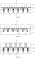
- a protective layer 236 is formed on each of a surface of the active region 213 and sidewall and bottom surfaces of the first trench and the second trench.
- the protective layer 236 protects the active region 213 during a subsequent process (etching, implantation, or other processes).
- a material of the protective layer 236 may be one or more of silicon oxide, silicon nitride, silicon oxynitride, and silicon nitride bonded silicon carbide.
- the material of the protective layer 236 may be silicon oxide, and the protective layer 236 may be formed by using a furnace tube oxidation process, a thermal oxidation process, or a deposition process.
- a third trench 217 extending along the first direction is formed in a portion of the semiconductor substrate 201 at the bottom of the first trench 214.
- a width of the third trench 217 is less than a width of the bottom of the first trench 214.
- the third trench 217 is formed for the purpose of separating adjacent active regions 213 that are arranged along the second direction, and defining positions of bit line doped regions (specifically, portions of the semiconductor substrate on two sides of the third trench are used as bit line doped regions of corresponding transistors).
- Each portion of the semiconductor substrate 201 at the bottom of the first trench 214 has a corresponding third trench 217.
- a width of the first trench 214 is less than the width of the bottom of the first trench 214. In some embodiments, the width of the first trench 214 is 1/4 to 3/4 of the width of the bottom of the first trench 214.
- the portion of the semiconductor substrate 201 at the bottom of the first trench 214 is etched to form the third trench 217 extending along the first direction.
- a third mask layer is formed in the first trench 214 and on the semiconductor substrate 201, and a sixth opening extending along the first direction and exposing a surface of a portion of the semiconductor substrate 201 at the bottom of the first trench 214 is formed in the third mask layer.
- the semiconductor substrate 201 is etched along the sixth opening to form the third trench 217.
- the etching is anisotropic dry etching, and may anisotropic plasma etching.
- the third mask layer is removed.
- bit line doped regions 217 are formed in portions of the semiconductor substrate 201 on two sides of the third trench 217 and at the bottom of the first trench 214 through an ion implantation process.
- the bit line doped region 217 is subsequently used as a bit line of a memory, a portion of the bit line doped region in contact with each active region 213 may be used as a drain region of a subsequently formed vertical transistor in each active region, and after the vertical transistor is subsequently formed, the bit line may be used to perform a read or write operation on a row of memories arranged along the first direction.
- the bit line doped region 217 is formed through ion implantation.
- a type of impurity ions implanted in the bit line doped region 217 is different from a type of impurity ions implanted in the active region 213.
- P-type impurity ions are implanted in the active region 213, N-type impurity ions are implanted in the bit line doped region 217, or when N-type impurity ions are implanted in the active region 213, P-type impurity ions are implanted in the bit line doped region 217.
- the impurity ions implanted in the bit line doped region 217 are N-type impurity ions or P-type impurity ions.
- the P-type impurity ions are one or more of boron ions, gallium ions, or indium ions.
- the N-type impurity ions are one or more of phosphorus ions, arsenic ions, or antimony ions.
- a fourth mask layer 238 is formed in the third trench 217 and on the top surface of the active region 213, and a seventh opening extending along the first direction and exposing the portions of the semiconductor substrate 201 on the two sides of the third trench 217 is formed in the fourth mask layer 238.
- first ion implantation is formed on a portion of the semiconductor substrate 201 at the bottom of the seventh opening along the seventh opening, and the bit line doped regions 218 are formed in the portions of the semiconductor substrate 201 on the two sides of the third trench 217 and at the bottom of the first trench 214.
- bit line doped regions 218, the fourth mask layer 238 is removed.
- the bit line doped regions 218 are distributed in the portions of the semiconductor substrate 201 on two sides of the active region 213, such that a control capability of the bit line can be improved and electrical properties of the memory can be improved.
- the first ion implantation has energy of 20 kev to 100 kev, a dose of 1E13 to 1E22 atom/cm 2 , and an angle of 0 degrees to 20 degrees.
- a gate dielectric layer 216 is formed on sidewall surfaces and a bottom surface of each of the first trench 214 and the second trench 215.
- a material of the gate dielectric layer 216 may be silicon oxide or a high-K (dielectric constant) dielectric material.
- the high-K dielectric material is one or more of HfO 2 , TiO 2 , HfZrO, HfSiNO, Ta 2 O 5 , ZrO 2 , ZrSiO 2 , Al 2 O 3 , SrTiO 3 , or BaSrTiO.
- the gate dielectric layer 216 may be formed by using an oxidation process or a deposition process.
- the gate dielectric layer 216 may be formed after the removal of the protective layer 236. In another embodiment, a gate dielectric layer may be formed directly on the protective layer 236 without removing the protective layer 236.
- the gate dielectric layer 216 may alternatively be formed on sidewall and bottom surfaces of the third trench or directly fill the third trench.
- a first dielectric layer 219 that fills the third trench is formed.
- the formed first dielectric layer 219 is used for electrical isolation between adjacent word line doped regions 218.
- a material of the first dielectric layer 219 is silicon oxide, silicon nitride, silicon oxynitride, fluorine-doped silica glass (FSG), a low dielectric constant (where K is less than 2.8) material, other suitable materials, and/or a combination thereof.
- a formation process of the first dielectric layer 219 includes: forming a first dielectric material layer on a surface of the active region 213 and in the first trench 214, the second trench 215, and the third trench by using a deposition process; and etching back to remove a portion of the first dielectric material layer, to form the first dielectric layer 219 that fills the third trench.
- the formed first dielectric layer 219 fills the third trench, and a surface of the first dielectric layer 219 may be higher than an opening of the third trench and partially located in the first trench 214.
- a metal gate 220 is formed in each of the first trench 214 on the first dielectric layer 219 and the second trench 215.
- a top surface of the metal gate 220 is lower than a top surface of the active region 213.
- the formed metal gate 220 is located in the second trench 215 and the first trench 214, that is, the formed metal gate 220 surrounds sidewalls of each active region, such that a capability of the metal gate 220 to control the formation of a trench in the sidewall of the active region can be improved, and performance of forming a vertical transistor can be improved.
- a material of the metal gate 220 may be one or more of W, Al, Cu, Ag, Au, Pt, Ni, Ti, TiN, TaN, Ta, TaC, TaSiN, WN, and Wsi.
- a formation process the metal gate 220 is: forming a metal layer in the first trench and the second trench and on a surface of the active region; and etching back to remove a portion of the metal layer, and using the remaining metal layer in the first trench and the second trench as the metal gate 220, where a surface of the metal gate 220 is lower than the top surface of the active region 213.
- each of the second trench and the first trench above the metal gate 220 is filled with a second dielectric layer 221; and a portion of the metal gate 220 in the second trench 215 is etched to segment the metal gate 220 in the second trench along the second direction.
- the metal gate 220 is segmented along the second direction, such that multiple sub-metal gates extending along the second direction and parallel to each other can be formed, and each sub-metal gate can correspondingly control multiple vertical transistors formed in multiple active regions in a row along the second direction.
- a portion of the metal gate 220 in the second trench is segmented along the second direction, to form a fifth mask layer 222 on a surface of the second dielectric layer 221 and a top surface of the active region 213, and an eighth opening extending along the second direction and exposing a surface of a portion of the second dielectric layer 221 in the second trench is formed in the fifth mask layer 222; and portions of the second dielectric layer 221 and the metal gate 220 in the second trench are etched along the eighth opening to segment the metal gate in the second trench.
- a material of the second dielectric layer 221 is silicon oxide, silicon nitride, silicon oxynitride, FSG, a low dielectric constant (where K is less than 2.8) material, other suitable materials, and/or a combination thereof.
- the second mask layer 222 (referring to FIG. 28 and FIG. 29 ) is removed; gaps of the segmented metal gate 220 and the second trench are filled with a dielectric material, and the filled dielectric material is used as a portion of the second dielectric layer 221; and a source region 223 is formed on the top surface of the active region 213.
- a type of impurity ions doped in the source region 223 is the same as a type of impurity ions doped in the bit line doped region 218, and is different from the type of the impurity ions doped in the foregoing well region.
- the source region 223 is formed by using a second ion implantation process.
- the impurity ions implanted (doped) in the bit line doped region 217 are N-type impurity ions or P-type impurity ions.
- the P-type impurity ions are one or more of boron ions, gallium ions, or indium ions.
- the N-type impurity ions are one or more of phosphorus ions, arsenic ions, or antimony ions.
- each vertical transistor includes a corresponding active region 213, a gate dielectric layer 216 located on a sidewall surface of the active region 213, bit line doped regions 218 located in portions of a semiconductor substrate at the bottom of a first trench and on two sides of a third trench, a source region 223 located on a top surface of the active region 213, and a metal gate 220 located in each of the first trench and a second trench and surrounding the active region 213.
- a source region and a drain region are located on an upper side and a lower side of the active region, and a formed channel region is located on a sidewall of the active region, such that an area of the semiconductor substrate occupied by the vertical transistor is relatively small, a quantity of vertical transistors formed per unit area can be increased, and correspondingly, a quantity of capacitors connected to the source region of each transistor and subsequently formed per unit area can also be increased, thereby improving a storage capacity and storage density of a memory.
- use of the vertical transistor of such a specific structure can reduce a body effect, reduce a leakage current generated by a subsequently formed capacitor into the substrate, and improve electrical properties of the memory device.
- the following is further included: forming, on a surface of the semiconductor substrate 201, a capacitor connected to the source region 223.
- the process of forming, on a surface of the semiconductor substrate 201, a capacitor connected to the source region 223 includes: referring to FIG. 32 and FIG. 33 , forming a third dielectric layer 224 on the active region 213 and the second dielectric layer 221; and forming, in the third dielectric layer 224, a through hole 225 exposing a surface of the source region 223.
- the following step may further be included: widening an opening of the through hole 225 to facilitate subsequent formation of a contact plug, and to increase a contact area between a top surface of the formed contact plug and the subsequently formed capacitor. Referring to FIG. 36 and FIG.
- a contact plug 226 is formed in the through hole, and a material of the contact plug 226 is metal.
- a fourth dielectric layer 227 is formed on the third dielectric layer 224; a capacitor hole 229 exposing the contact plug is formed in the fourth dielectric layer 227; and a capacitor 228 is formed in the capacitor hole 229.
- the capacitor 228 includes a bottom electrode layer, a dielectric layer located on the bottom electrode layer, and a top electrode layer located on the dielectric layer.
- a material of the dielectric layer may be a high-K dielectric material, so as to increase a capacitance value of the capacitor per unit area.
- the high-K dielectric material includes one of HfO 2 , TiO 2 , HfZrO, HfSiNO, Ta 2 O 5 , ZrO 2 , ZrSiO 2 , Al 2 O 3 , SrTiOa, or BaSrTiO, or a stacked layer formed by at least two of groups including the foregoing materials.
- a material of each of the top electrode layer and the bottom electrode layer may be one of tungsten, titanium, nickel, aluminum, platinum, titanium nitride, N-type polycrystalline silicon, and P-type polycrystalline silicon, or a stacked layer formed by at least two of groups including the foregoing materials, or may include a compound formed by one or two of metal nitride and metal silicide, such as titanium nitride, titanium silicide, nickel silicide, or silicon titanium nitride (TiSixNy).
- the capacitor may alternatively be formed by using an existing double-sided capacitor formation process.
- the memory device includes:
- the multiple active regions 213 are arranged in rows and columns.
- the width of the third trench 217 is 3/4 to 1/4 of the width of the bottom of the first trench 214.
- impurity ions doped in the bit line doped region 218 are N-type impurity ions or P-type impurity ions.
- a type of impurity ions doped in the source region 223 is the same as a type of the impurity ions doped in the bit line doped region 218 and different from a type of impurity ions in a well region formed in the active region.
- the memory device further includes: a third dielectric layer 224, located on the active region 213 and the second dielectric layer 221, where a contact plug 226 connected to the source region 223 is formed in the third dielectric layer 224; and a fourth dielectric layer 227 located on the third dielectric layer 224, where a capacitor hole exposing the contact plug 226 is formed in the fourth dielectric layer 227, and the capacitor 228 is located in the capacitor hole.
- a material of the metal gate is one or more of W, Al, Cu, Ag, Au, Pt, Ni, Ti, TiN, TaN, Ta, TaC, TaSiN, WN, and Wsi.
Abstract
A memory device and a forming method thereof. The memory device includes: a semiconductor substrate, wherein multiple active regions are formed in the semiconductor substrate, and the multiple active regions are separated by multiple first trenches extending along a first direction and multiple second trenches extending along a second direction; a third trench, extending along the first direction and located in the semiconductor substrate at the bottom of the first trench; a bit line doped region, located in the semiconductor substrate on two sides of the third trench; a gate dielectric layer, located on a sidewall surface of the first trench and a sidewall surface of the second trench; a first dielectric layer that fills the third trench; a metal gate, located in the second trench and the first trench on the first dielectric layer and the second trench, wherein the metal gate in the second trench is segmented along the second direction; a source region, located on a top surface of the active region; and a capacitor, located on a surface of the semiconductor substrate and connected to the source region. Storage density of the memory device in the present invention is improved.
Description
- The present application claims the priority to
Chinese Patent Application No. 202110966709.7, titled " MEMORY DEVICE AND FORMING METHOD THEREOF", filed with China National Intellectual Property Administration (CNIPA) on August 23, 2021 - The present application relates to the field of memories, and in particular, to a memory device and a forming method thereof.
- As a commonly used semiconductor memory in computers, a dynamic random access memory (DRAM) is composed of many repeated memory cells. Each memory cell usually includes a capacitor and a transistor. In the transistor, a gate is connected to a word line (WL), a drain is connected to a bit line (BL), and a source is connected to the capacitor. A voltage signal on the WL can control the transistor to turn on or off, and then data information stored in the capacitor is read through the BL, or data information is written into the capacitor through the BL for storage.
- In order to improve integration of a memory structure, the transistor in the existing DRAM usually uses a trench-type transistor structure. However, a line width of a transistor structure of the existing trench-type has been minimized and a storage capacity of the DRAM cannot be further improved. Therefore, how to further improve the storage capacity and storage density of the DRAM is an urgent problem to be resolved by those skilled in the art.
- In view of this, the present application provides a novel memory device and a forming method thereof, which can further improve a storage capacity and storage density of the memory device.
- Therefore, some embodiments of the present application provide a method of forming a memory device, including:
providing a semiconductor substrate, wherein multiple active regions are formed in the semiconductor substrate, the multiple active regions are separated by multiple first trenches extending along a first direction and multiple second trenches extending along a second direction, and the first trench communicates with the corresponding second trench; forming, in the semiconductor substrate at a bottom of the first trench, a third trench extending along the first direction, wherein a width of the third trench is less than a width of the bottom of the first trench; forming a bit line doped region in the semiconductor substrate on two sides of the third trench and at the bottom of the first trench through an ion implantation process; forming a gate dielectric layer on a sidewall surface and a bottom surface of the first trench and a sidewall surface and a bottom surface of the second trench; forming a first dielectric layer that fills the third trench; forming a metal gate in the second trench and the first trench on the first dielectric layer, wherein a top surface of the metal gate is lower than a top surface of the active region; filling the second trench and the first trench above the metal gate with a second dielectric layer; etching a portion of the metal gate in the second trench, and segmenting the metal gate in the second trench along the second direction; forming a source region on the top surface of the active region; and forming, on a surface of the semiconductor substrate, a capacitor connected to the source region. - In some embodiments, the multiple active regions are arranged in rows and columns.
- In some embodiments, a formation process of the multiple active regions includes: forming, on the semiconductor substrate, multiple first mask patterns extending along the first direction and parallel to each other, with a first opening formed between adjacent first mask patterns; forming, on the first mask patterns, multiple second mask patterns extending along the second direction and parallel to each other, with a second opening formed between adjacent second mask patterns; etching the first mask pattern along the second opening by using the second mask pattern as a mask, and segmenting the first mask pattern along the second direction, and forming multiple discrete block mask patterns; and etching the semiconductor substrate by using each of the block mask patterns as a mask, and forming, in the semiconductor substrate, the first trench corresponding to the first opening and the second trench corresponding to the second opening, wherein the retained semiconductor substrate between the first trench and the second trench is the multiple active regions.
- In some embodiments, the first mask pattern and the second mask pattern are formed by using a self-aligned double patterning process.
- In some embodiments, a formation process of the first mask pattern includes: forming a first hard mask layer on the semiconductor substrate; forming, on the first hard mask layer, multiple first strip structures extending along the first direction and arranged parallel to each other; forming a first sacrificial sidewall layer on a sidewall and a top surface of the first strip structure and on the first hard mask layer between the first strip structures; filling each portion between the first strip structures with a first filling layer; removing the first sacrificial sidewall layer on the sidewall surface of the first strip structure, and forming a third opening between the first strip structure and the first filling layer; and etching the first hard mask layer along the third opening, and forming the first opening in the first hard mask layer, and using the retained portion of the first hard mask layer as the first mask pattern.
- In some embodiments, a formation process of the second mask pattern includes: forming a second hard mask layer on the semiconductor substrate and the first mask pattern; forming, on the second hard mask layer, multiple second strip structures arranged in parallel along the second direction; forming a second sacrificial sidewall layer on a sidewall and a top surface of the second strip structure and on a surface of the second hard mask layer between the second strip structures; filling each portion between the second strip structures with a second filling layer; removing the second sacrificial sidewall layer on the sidewall surface of the second strip structure, and forming a fourth opening between the second strip structure and a second filling layer; and etching the second hard mask layer along the fourth opening, and forming the second opening in the second hard mask layer, and using the retained portion of the second hard mask layer as the second mask pattern.
- In some embodiments, the width of the third trench is 1/4 to 3/4 of the width of the bottom of the first trench.
- In some embodiments, a formation process of the third trench includes: forming a third mask layer in the first trench, with a sixth opening formed in the third mask layer, extending along the first direction, and exposing a surface of a portion of the semiconductor substrate at the bottom of the first trench; and etching the semiconductor substrate along the sixth opening, and forming the third trench.
- In some embodiments, the process of forming a bit line doped region in the semiconductor substrate on two sides of the third trench and at the bottom of the first trench through an ion implantation process includes: forming a fourth mask layer in the third trench and on the top surface of the active region, with a seventh opening formed in the fourth mask layer, extending along the first direction, and exposing the semiconductor substrate on the two sides of the third trench; and performing first ion implantation on the semiconductor substrate at the bottom of the seventh opening along the seventh opening, and forming the bit line doped regions in the semiconductor substrate on the two sides of the third trench and at the bottom of the first trench.
- In some embodiments, impurity ions implanted through the first ion implantation are N-type impurity ions or P-type impurity ions, and the first ion implantation has energy of 20 kev to 100 kev, a dose of 1E13 to 1E22 atom/cm2, and an angle of 0 to 20 degrees.
- In some embodiments, the source region is formed through second ion implantation, and a type of impurity ions implanted in the source region is the same as a type of impurity ions implanted in the bit line doped region.
- In some embodiments, the process of forming, on a surface of the semiconductor substrate, a capacitor connected to the source region includes: forming a third dielectric layer on the active region and the second dielectric layer; forming, in the third dielectric layer, a through hole exposing a surface of the source region; forming a contact plug in the through hole; forming a fourth dielectric layer on the third dielectric layer; forming, in the fourth dielectric layer, a capacitor hole exposing the contact plug; and forming the capacitor in the capacitor hole.
- In some embodiments, doping is performed in a well region on the semiconductor substrate, and a type of impurity ions doped in the well region is opposite to a type of impurity ions doped in the source region and a type of impurity ions doped in the bit line doped region.
- Some other embodiments of the present invention further provide a memory device, including:
a semiconductor substrate, wherein multiple active regions are formed in the semiconductor substrate, the multiple active regions are separated by multiple first trenches extending along a first direction and multiple second trenches extending along a second direction, and the first trench communicates with the corresponding second trench; a third trench, extending along the first direction and located in the semiconductor substrate at a bottom of the first trench, wherein a width of the third trench is less than a width of the bottom of the first trench; a bit line doped region, located in the semiconductor substrate on two sides of the third trench and at the bottom of the first trench; a gate dielectric layer, located on a sidewall surface of the first trench and the second trench; a first dielectric layer that fills the third trench; a metal gate, located in the second trench and the first trench on the first dielectric layer, wherein a top surface of the metal gate is lower than a top surface of the active region, and the metal gate in the second trench is segmented along the second direction; a second dielectric layer that fills the second trench and the first trench located above the metal gate; a source region, located on the top surface of the active region; and a capacitor, located on a surface of the semiconductor substrate and connected to the source region. - In some embodiments, the multiple active regions are arranged in rows and columns.
- In some embodiments, the width of the third trench is 1/4 to 3/4 of the width of the bottom of the first trench.
- In some embodiments, impurity ions doped in the bit line doped region are N-type impurity ions or P-type impurity ions.
- In some embodiments, a type of impurity ions doped in the source region is the same as a type of the impurity ions doped in the bit line doped region.
- In some embodiments, the memory device further includes: a third dielectric layer, located on the active region and the second dielectric layer, wherein a contact plug connected to the source region is formed in the third dielectric layer; and a fourth dielectric layer located on the third dielectric layer, wherein a capacitor hole exposing the contact plug is formed in the fourth dielectric layer, and the capacitor is located in the capacitor hole.
- In some embodiments, a material of the metal gate is one or more of W, Al, Cu, Ag, Au, Pt, Ni, Ti, TiN, TaN, Ta, TaC, TaSiN, WN, and Wsi.
- According to the method of forming a memory device provided in some embodiments described above in the present application, multiple active regions are formed in the semiconductor substrate, and after the multiple active regions are separated by multiple first trenches extending along a first direction and multiple second trenches extending along a second direction, a third trench extending along the first direction is formed in a portion of the semiconductor substrate at the bottom of each of the first trenches, where a width of the third trench is less than a width of the bottom of the first trench; bit line doped regions are formed in portions of the semiconductor substrate on two sides of the third trench and at the bottom of the first trench through an ion implantation process; a gate dielectric layer is formed on sidewall surfaces and a bottom surface of each of the first trench and the second trench; a first dielectric layer that fills the third trench is formed; a metal gate is formed in each of the first trench on the first dielectric layer and the second trench, where a top surface of the metal gate is lower than a top surface of the active region; a portion of each of the first trench and the second trench above the metal gate is filled with a second dielectric layer; a portion of the metal gate in the second trench is etched to segment the metal gate in the second trench along the second direction; a source region is formed on the top surface of the active region; and a capacitor connected to the source region is formed on a surface of the semiconductor substrate. In a manufacturing process of a memory device in the present application, multiple vertical transistors are formed through the foregoing process, and each vertical transistor includes a corresponding active region, a gate dielectric layer located on a sidewall surface of the active region, bit line doped regions located in portions of a semiconductor substrate at the bottom of a first trench and on two sides of a third trench, a source region located on a top surface of the active region, and a metal gate located in each of the first trench and a second trench and surrounding the active region. In the foregoing vertical transistor of a specific structure, a source region and a drain region are located on an upper side and a lower side of the active region, and a formed channel region is located on a sidewall of the active region, such that an area of the semiconductor substrate occupied by the vertical transistor is relatively small, a quantity of vertical transistors formed per unit area can be increased, and correspondingly, a quantity of capacitors connected to the source region of each transistor and subsequently formed per unit area can also be increased, thereby improving a storage capacity and storage density of a memory. In addition, use of the vertical transistor of such a specific structure can reduce a body effect, reduce a leakage current generated by a subsequently formed capacitor into the substrate, and improve electrical properties of the memory device.
-
FIG. 1 to FIG. 39 are each a schematic structural diagram of a formation process of a memory device according to an embodiment of the present application. - As described in the background, how to further improve the storage capacity and storage density of the DRAM is an urgent problem to be resolved by those skilled in the art.
- Researches have found that a trench-type transistor usually includes at least one buried word line located in a semiconductor substrate and one drain region and at least one source region located in portions of the semiconductor substrate on two sides of the buried word line. Such a trench-type transistor occupies a relatively large area of the semiconductor substrate, which is not conducive to improvement of integration of the DRAM, thus limiting the storage capacity and storage density of the DRAM.
- Therefore, the present application provides a novel memory device and a forming method thereof, which can further improve a storage capacity and storage density of the memory device.
- To make the above objectives, features and advantages of the present application clearer, specific implementations of the present application will be described below in detail with reference to accompanying drawings. In detailed descriptions on embodiments of the present application, schematic views are not partially enlarged according to a general proportion for ease of descriptions. The schematic views merely serve as examples, rather than limitations to the scope of protection of the present application. In addition, dimensions in a three-dimensional (3D) space including a length, width and depth should be provided in actual manufacture.
- Referring to
FIG. 13 to FIG. 15, FIG. 13 is a schematic structural diagram of a cross section ofFIG. 15 along a direction of a cutting line AB,FIG. 14 is a schematic structural diagram of a cross section ofFIG. 15 along a direction of a cutting line CD, and asemiconductor substrate 201 is provided. Multipleactive regions 213 are formed in thesemiconductor substrate 201, and the multipleactive regions 213 are separated by multiplefirst trenches 214 extending along a first direction and multiplesecond trenches 215 extending along a second direction. Thefirst trench 214 communicates with the correspondingsecond trench 215. - A material of the
semiconductor substrate 201 may be silicon (Si), germanium (Ge), silicon-germanium (GeSi), or silicon carbide (SiC); or may be silicon on insulator (SOI) or germanium on insulator (GOI); or may be another material such as gallium arsenide or other III-V compounds. In this embodiment, the material of thesemiconductor substrate 201 is silicon. Thesemiconductor substrate 201 needs to be doped with some impurity ions according to a type of a subsequently formed vertical transistor. For example, doping may be performed in a well region on the semiconductor substrate. The impurity ions may be N-type impurity ions or P-type impurity ions. The P-type impurity ions are one or more of boron ions, gallium ions, or indium ions. The N-type impurity ions are one or more of phosphorus ions, arsenic ions, or antimony ions. - The
active region 213 is subsequently used to form a channel region of the vertical transistor. The multipleactive regions 213 are discrete, and adjacentactive regions 213 separated by cross-distributedfirst trenches 214 andsecond trenches 215. - In some embodiments, the formed
active regions 213 are arranged in rows and columns (referring toFIG. 15 ). In other embodiments, the active regions may be arranged in another manner. - In some embodiments, the first direction and the second direction are perpendicular to each other and have an angle of 90 degrees. In other embodiments, the first direction and the second direction may not be perpendicular to each other. For example, an angle between the first direction and the second direction may be an acute angle.
- In some embodiments, the
semiconductor substrate 201 may be first etched to form multiplefirst trenches 214, and then thesemiconductor substrate 201 is etched to form multiplesecond trenches 215, thereby forming multiple discreteactive regions 213. In other embodiments, thefirst trench 214 and thesecond trench 215 may be formed simultaneously by etching thesemiconductor substrate 201. - In this embodiment, the multiple
active regions 213 are formed by using a self-aligned double patterning mask process. A formation process of theactive region 213 is described in detail below with reference toFIG. 1 to FIG. 15 . - Referring to
FIG. 1 , a firsthard mask layer 202 is formed on thesemiconductor substrate 201; and afirst material layer 203 is formed on the firsthard mask layer 202. - The first
hard mask layer 202 is subsequently used to form a first mask pattern. In some embodiments, the firsthard mask layer 202 may be of a single-layer structure or a multi-layer stacked structure. A material of the firsthard mask layer 202 may be one or more of polycrystalline silicon, amorphous silicon, amorphous carbon, silicon nitride, silicon oxynitride, silicon oxide, silicon nitride bonded silicon carbide, silicon oxycarbide, silicon carbide, and silicon-germanium. A process of forming the firsthard mask layer 202 may be atmospheric or low pressure chemical vapor deposition (CVD), plasma enhanced chemical vapor deposition (PECVD), thermal chemical vapor deposition (Thermal CVD), physical vapor deposition (PVD), atomic layer deposition (ALD), sputtering, metallization, electroplating, spin coating, other suitable methods, and/or a combination thereof. In this embodiment, the material of the firsthard mask layer 202 is polycrystalline silicon. - In some embodiments, a first etching stop layer (not shown in the figure) may further be formed between the first
hard mask layer 202 and thesemiconductor substrate 201. The first etching stop layer is used to protect an underlying material layer from being over-etched during patterning of the first hard mask layer. A material of the first etching stop layer is different from that of the first hard mask layer. The material of the first etching stop layer is one or more of silicon nitride, silicon oxynitride, silicon oxide, silicon nitride bonded silicon carbide, and silicon oxycarbide. In this embodiment, the material of the first etching stop layer is silicon oxide. - The
first material layer 203 is subsequently used to form a first strip structure. In some embodiments, thefirst material layer 203 may be of a single-layer structure or a multi-layer stacked structure. A material of thefirst material layer 203 may be one or more of polycrystalline silicon, amorphous silicon, amorphous carbon, silicon nitride, silicon oxynitride, silicon oxide, silicon nitride bonded silicon carbide, silicon oxycarbide, silicon carbide, and silicon-germanium. In this embodiment, the material of thefirst material layer 203 is amorphous carbon. - In some embodiments, a second etching stop layer (not shown in the figure) may further be formed between the
first material layer 203 and the firsthard mask layer 202. The second etching stop layer is used to protect an underlying material layer from being over-etched during patterning of thefirst material layer 203. A material of the second etching stop layer is different from that of thefirst material layer 203. The material of the second etching stop layer is one or more of silicon nitride, silicon oxynitride, silicon oxide, silicon nitride bonded silicon carbide, and silicon oxycarbide. In this embodiment, the material of the second etching stop layer is silicon oxynitride. - Referring to
FIG. 2 and FIG. 3, FIG. 2 is a schematic structural diagram of a cross section ofFIG. 3 along a direction of a cutting line AB. The first material layer 203 (referring toFIG. 1 ) is patterned. Multiplefirst strip structures 204 extending along the first direction and arranged parallel to each other are formed on the first hard mask layer. - The
first strip structure 204 is elongated. The multiplefirst strip structures 204 are discrete and parallel to each other. Afourth opening 205 is formed between adjacentfirst strip structures 204. - In some embodiments, the
first material layer 203 is patterned by using an anisotropic dry etching process, and specifically, an anisotropic plasma etching process may be used. - In some embodiments, before the
first material layer 203 is patterned, a patterned photoresist layer (not shown in the figure) may further be formed on thefirst material layer 203, and thefirst material layer 203 is etched by using the patterned photoresist layer as a mask to form afirst strip structure 204; and the patterned photoresist layer is removed. - Referring to
FIG. 4, FIG. 4 is performed on the basis ofFIG. 2 , and a firstsacrificial sidewall layer 206 is formed on sidewall and top surfaces of thefirst strip structure 204 and on a portion of the firsthard mask layer 202 betweenfirst strip structures 204. - A material of the first
sacrificial sidewall layer 206 is different from that of the first strip structure. The material of the firstsacrificial sidewall layer 206 may be one or more of polycrystalline silicon, amorphous silicon, amorphous carbon, silicon nitride, silicon oxynitride, silicon oxide, silicon nitride bonded silicon carbide, silicon oxycarbide, silicon carbide, and silicon-germanium. The firstsacrificial sidewall layer 206 is formed by using a deposition process. The deposition process includes an atomic layer deposition process. - Referring to
FIG. 5 , each portion between thefirst strip structures 204 is filled with afirst filling layer 207, and thefirst filling layer 207 fills the remaining portion of the fourth opening. - Subsequently, a third opening is formed between the
first strip structure 204 and thefirst filling layer 207 by removing portions of the first sacrificial sidewall layer on the sidewall surfaces of thefirst strip structure 204. - A material of the
first filling layer 207 is different from that of the firstsacrificial sidewall layer 206. In some embodiments, the material of thefirst filling layer 207 may be one or more of polycrystalline silicon, amorphous silicon, amorphous carbon, silicon nitride, silicon oxynitride, silicon oxide, silicon nitride bonded silicon carbide, silicon oxycarbide, silicon carbide, silicon-germanium, and an organic material. A process of forming thefirst filling layer 207 may be atmospheric or low pressure CVD, PECVD, thermal CVD, PVD, ALD, sputtering, metallization, electroplating, spin coating, other suitable methods, and/or a combination thereof. - In some embodiments, a surface of the formed first filling
layer 207 may be flush with the firstsacrificial sidewall layer 206 on the top surface of thefirst strip structure 204. Specifically, after a first filling material layer covering the firstsacrificial sidewall layer 206 and filling the remaining portion of the fourth opening is formed, a portion of the first filling layer above the firstsacrificial sidewall layer 206 on the top surface of thefirst strip structure 204 is removed by using a chemical-mechanical mask process. The remaining portion of the first filling material layer in the fourth opening is used as thefirst filling layer 207. - In some embodiments, a surface of the formed first filling layer may be flush with the top surface of the
first strip structure 204. Specifically, after a first filling material layer covering the firstsacrificial sidewall layer 206 and filling the remaining portion of the fourth opening is formed, a portion of the firstsacrificial sidewall layer 206 and the first filling material layer above the top surface of thefirst strip structure 204 are removed by using a chemical-mechanical mask process, to expose the top surface of thefirst strip structure 204, and the remaining portion of the first filling material layer in the fourth opening is used as the first filling layer. Therefore, a top surface of the formed first filling layer is flush with the top surface of the first strip structure. After the third opening is subsequently formed, during etching of the first hard mask layer, an etching load effect caused by a height difference between the filling layer and the first strip structure can be alleviated, accuracy of positions and sizes of the formed first mask patterns can be improved, and a favorable sidewall shape can be maintained, such that positions and sizes of block mask patterns formed after the first mask patterns are segmented have relatively high accuracy and a favorable sidewall shape is maintained, and finally, positions and sizes of active regions formed by etching the semiconductor substrate by using each of the block mask patterns as a mask have relatively high accuracy and a favorable sidewall shape is maintained. - Referring to
FIG. 6 , portions of the first sacrificial sidewall layer on the sidewall surfaces of thefirst strip structure 204 are removed, to form athird opening 208 between thefirst strip structure 204 and thefirst filling layer 207. - In some embodiments, the portions of the first sacrificial sidewall layer on the sidewall surfaces of the
first strip structure 204 are removed by using an anisotropic dry etching process, including an anisotropic plasma etching process. - It should be noted that, in some embodiments, during the removal of the portions of the first sacrificial sidewall layer on the sidewall surfaces of the
first strip structure 204, the portion of the first sacrificial sidewall layer on the top surface of thefirst strip structure 204 is also removed. - Referring to
FIG. 7 to FIG. 9, FIG. 7 is performed on the basis ofFIG. 6 ,FIG. 7 is a schematic structural diagram of a cross section ofFIG. 9 along a direction of a cutting line AB, andFIG. 8 is a schematic structural diagram of a cross section ofFIG. 9 along a direction of a cutting line CD. The first hard mask layer 202 (referring toFIG. 6 ) is etched along the third opening 208 (referring toFIG. 6 ), to form thefirst opening 210 in the first hard mask layer, and the retained portion of the first hard mask layer is used as thefirst mask pattern 209. - In some embodiments, the first
hard mask layer 202 is etched by using an anisotropic dry etching process, including an anisotropic plasma etching process. - The formed multiple
first mask patterns 209 are discrete. Specifically, the formedfirst mask patterns 209 extend along the first direction and are parallel to each other, and afirst opening 210 is formed between adjacentfirst mask patterns 209. - In the present application, the foregoing
first mask pattern 209 is formed by using the foregoing self-aligned double patterning process, and subsequently, during the formation of the active region, a width of the first trench between active regions can be made relatively small, thereby allowing an area of the active region to be relatively large. - Referring to
FIG. 10 to FIG. 12, FIG. 10 is a schematic structural diagram of a cross section ofFIG. 12 along a direction of a cutting line AB, andFIG. 11 is a schematic structural diagram of a cross section ofFIG. 12 along a direction of a cutting line CD. The first mask patterns 209 (referring toFIG. 7 to FIG. 9 ) are segmented along the second direction to form multiple discreteblock mask patterns 211. - The first mask patterns 209 (referring to
FIG. 7 to FIG. 9 ) are segmented along the second direction by using an anisotropic dry etching process. In some embodiments, before thefirst mask patterns 209 are segmented along the second direction, multiple second mask patterns extending along the second direction and parallel to each other are formed on thefirst mask pattern 209 and are each used as a mask for etching thefirst mask patterns 209, and a second opening is formed between adjacent second mask patterns; thefirst mask patterns 209 are etched along the second opening by using each of the second mask patterns as a mask, to segment the first mask patterns along the second direction to form multiple discreteblock mask patterns 211; and the second mask patterns are removed. - In some embodiments, the second mask pattern may be formed by using a self-aligned double patterning process. A specific process includes: A formation process of the second mask pattern includes: forming a second hard mask layer on the semiconductor substrate and the first mask pattern; forming, on the second hard mask layer, multiple second strip structures arranged in parallel along the second direction; form a second sacrificial sidewall layer on a sidewall and top surfaces of the second strip structure and on a surface of a portion of the second hard mask layer between second strip structures; filling each portion between the second strip structures with a second filling layer; removing portions of the second sacrificial sidewall layer on the sidewall surfaces of the second strip structure, to form a fourth opening between the second strip structure and a second filling layer; and etching the second hard mask layer along the fourth opening, to form the second opening in the second hard mask layer, and using the retained portion of the second hard mask layer as the second mask pattern.
- A material of the second hard mask layer may be one or more of polycrystalline silicon, amorphous silicon, amorphous carbon, silicon nitride, silicon oxynitride, silicon oxide, silicon nitride bonded silicon carbide, silicon oxycarbide, silicon carbide, and silicon-germanium. A process of forming the second hard mask layer may be atmospheric or low pressure CVD, PECVD, thermal CVD, PVD, ALD, sputtering, metallization, electroplating, spin coating, other suitable methods, and/or a combination thereof.
- In some embodiments, a fourth etching stop layer may further be formed between the second hard mask layer and the
first mask pattern 209. A material of the fourth etching stop layer is different from that of the second hard mask layer. The material of the fourth etching stop layer is one or more of silicon nitride, silicon oxynitride, silicon oxide, silicon nitride bonded silicon carbide, and silicon oxycarbide. - A material of the second strip structure may be one or more of polycrystalline silicon, amorphous silicon, amorphous carbon, silicon nitride, silicon oxynitride, silicon oxide, silicon nitride bonded silicon carbide, silicon oxycarbide, silicon carbide, and silicon-germanium. In some embodiments, the second strip structure may be formed by etching a second material layer located on the second hard mask layer. In some embodiments, a fifth etching stop layer may be further formed between the second material layer and the second hard mask layer. A material of the fifth etching stop layer is different from that of the second material layer. The material of the fifth etching stop layer is one or more of silicon nitride, silicon oxynitride, silicon oxide, silicon nitride bonded silicon carbide, and silicon oxycarbide.
- A material of the second sacrificial sidewall layer is different from that of the second strip structure. The material of the second sacrificial sidewall layer may be one or more of polycrystalline silicon, amorphous silicon, amorphous carbon, silicon nitride, silicon oxynitride, silicon oxide, silicon nitride bonded silicon carbide, silicon oxycarbide, silicon carbide, and silicon-germanium. The second sacrificial sidewall layer is formed by using a deposition process. The deposition process includes an atomic layer deposition process.
- A material of the second filling layer is different from that of the second sacrificial sidewall layer. In some embodiments, the material of the second filling layer may be one or more of polycrystalline silicon, amorphous silicon, amorphous carbon, silicon nitride, silicon oxynitride, silicon oxide, silicon nitride bonded silicon carbide, silicon oxycarbide, silicon carbide, silicon-germanium, and an organic material. A process of forming the second filling layer may be atmospheric or low pressure CVD, PECVD, thermal CVD, PVD, ALD, sputtering, metallization, electroplating, spin coating, other suitable methods, and/or a combination thereof.
- In some embodiments, a surface of the formed second filling layer may be flush with the second sacrificial sidewall layer on the top surface of the second strip structure. Specifically, after a second filling material layer covering the second sacrificial sidewall layer and filling a space between second strip structures is formed, a portion of the second filling layer above the surface of the second sacrificial sidewall layer on the top surface of the second strip structure is removed by using a chemical-mechanical mask process. The remaining portion of the second filling material layer between the second strip structures is used as the second filling layer.
- In some embodiments, a surface of the formed second filling layer may be flush with the top surface of the second strip structure. Specifically, after a second filling material layer covering the second sacrificial sidewall layer and filling a space between second strip structures is formed, a portion of the second sacrificial sidewall layer and the second filling material layer above the top surface of the second strip structure are removed by using a chemical-mechanical mask process, to expose the top surface of the second strip structure, and the remaining portion of the second filling material layer in the space between the second strip structures is used as the second filling layer. Therefore, a top surface of the formed second filling layer is flush with the top surface of the second strip structure. After the fourth opening is subsequently formed, during etching of the second hard mask layer, an etching load effect caused by a height difference between the filling layer and the second strip structure can be alleviated, accuracy of positions and sizes of the formed second mask patterns can be improved, and a favorable sidewall shape can be maintained, such that positions and sizes of block mask patterns formed after the first mask patterns are segmented have relatively high accuracy and a favorable sidewall shape is maintained, and finally, positions and sizes of active regions formed by etching the semiconductor substrate by using each of the block mask patterns as a mask have relatively high accuracy and a favorable sidewall shape is maintained.
- In some embodiments, the portions of the first sacrificial sidewall layer on the sidewall surfaces of the second strip structure are removed by using an anisotropic dry etching process, including an anisotropic plasma etching process.
- Referring to
FIG. 13 to FIG. 15, FIG. 13 is a schematic structural diagram of a cross section ofFIG. 15 along a direction of a cutting line AB, andFIG. 14 is a schematic structural diagram of a cross section ofFIG. 15 along a direction of a cutting line CD. Thesemiconductor substrate 201 is etched by using each of the block mask patterns (referring toFIG. 11 ) as a mask, to form, in thesemiconductor substrate 201,first trenches 214 corresponding to the first openings andsecond trenches 215 corresponding to the second openings. Multiplefirst trenches 214 extend along the first direction and are parallel to each other. Multiplesecond trenches 215 extend along the second direction and are parallel to each other. Eachfirst trench 214 communicates with a correspondingsecond trench 215. The retained portions of the semiconductor substrate between thefirst trenches 214 and thesecond trenches 215 are multipleactive regions 213. - In some embodiments, referring to
FIG. 16 andFIG. 17 ,FIG. 16 is performed on the basis ofFIG. 13 ,FIG. 17 is performed on the basis ofFIG. 14 , and aprotective layer 236 is formed on each of a surface of theactive region 213 and sidewall and bottom surfaces of the first trench and the second trench. - The
protective layer 236 protects theactive region 213 during a subsequent process (etching, implantation, or other processes). A material of theprotective layer 236 may be one or more of silicon oxide, silicon nitride, silicon oxynitride, and silicon nitride bonded silicon carbide. In this embodiment, the material of theprotective layer 236 may be silicon oxide, and theprotective layer 236 may be formed by using a furnace tube oxidation process, a thermal oxidation process, or a deposition process. - Referring to
FIG. 18 and FIG. 19 , athird trench 217 extending along the first direction is formed in a portion of thesemiconductor substrate 201 at the bottom of thefirst trench 214. A width of thethird trench 217 is less than a width of the bottom of thefirst trench 214. - The
third trench 217 is formed for the purpose of separating adjacentactive regions 213 that are arranged along the second direction, and defining positions of bit line doped regions (specifically, portions of the semiconductor substrate on two sides of the third trench are used as bit line doped regions of corresponding transistors). - Each portion of the
semiconductor substrate 201 at the bottom of thefirst trench 214 has a correspondingthird trench 217. A width of thefirst trench 214 is less than the width of the bottom of thefirst trench 214. In some embodiments, the width of thefirst trench 214 is 1/4 to 3/4 of the width of the bottom of thefirst trench 214. - In some embodiments, the portion of the
semiconductor substrate 201 at the bottom of thefirst trench 214 is etched to form thethird trench 217 extending along the first direction. Before thesemiconductor substrate 201 is etched, a third mask layer is formed in thefirst trench 214 and on thesemiconductor substrate 201, and a sixth opening extending along the first direction and exposing a surface of a portion of thesemiconductor substrate 201 at the bottom of thefirst trench 214 is formed in the third mask layer. Thesemiconductor substrate 201 is etched along the sixth opening to form thethird trench 217. The etching is anisotropic dry etching, and may anisotropic plasma etching. The third mask layer is removed. - Referring to
FIG. 20 to FIG. 23 , bit line dopedregions 217 are formed in portions of thesemiconductor substrate 201 on two sides of thethird trench 217 and at the bottom of thefirst trench 214 through an ion implantation process. - The bit line doped
region 217 is subsequently used as a bit line of a memory, a portion of the bit line doped region in contact with eachactive region 213 may be used as a drain region of a subsequently formed vertical transistor in each active region, and after the vertical transistor is subsequently formed, the bit line may be used to perform a read or write operation on a row of memories arranged along the first direction. - The bit line doped
region 217 is formed through ion implantation. A type of impurity ions implanted in the bit line dopedregion 217 is different from a type of impurity ions implanted in theactive region 213. For example, when P-type impurity ions are implanted in theactive region 213, N-type impurity ions are implanted in the bit line dopedregion 217, or when N-type impurity ions are implanted in theactive region 213, P-type impurity ions are implanted in the bit line dopedregion 217. The impurity ions implanted in the bit line dopedregion 217 are N-type impurity ions or P-type impurity ions. The P-type impurity ions are one or more of boron ions, gallium ions, or indium ions. The N-type impurity ions are one or more of phosphorus ions, arsenic ions, or antimony ions. - In some embodiments, before the ion implantation is performed, referring to
FIG. 20 andFIG. 21 , afourth mask layer 238 is formed in thethird trench 217 and on the top surface of theactive region 213, and a seventh opening extending along the first direction and exposing the portions of thesemiconductor substrate 201 on the two sides of thethird trench 217 is formed in thefourth mask layer 238. Referring toFIG. 22 and FIG. 23 , first ion implantation is formed on a portion of thesemiconductor substrate 201 at the bottom of the seventh opening along the seventh opening, and the bit line dopedregions 218 are formed in the portions of thesemiconductor substrate 201 on the two sides of thethird trench 217 and at the bottom of thefirst trench 214. After the formation of the bit line dopedregions 218, thefourth mask layer 238 is removed. The bit line dopedregions 218 are distributed in the portions of thesemiconductor substrate 201 on two sides of theactive region 213, such that a control capability of the bit line can be improved and electrical properties of the memory can be improved. - In some embodiments, the first ion implantation has energy of 20 kev to 100 kev, a dose of 1E13 to 1E22 atom/cm2, and an angle of 0 degrees to 20 degrees.
- Referring to
FIG. 24 andFIG. 25 , agate dielectric layer 216 is formed on sidewall surfaces and a bottom surface of each of thefirst trench 214 and thesecond trench 215. - A material of the
gate dielectric layer 216 may be silicon oxide or a high-K (dielectric constant) dielectric material. The high-K dielectric material is one or more of HfO2, TiO2, HfZrO, HfSiNO, Ta2O5, ZrO2, ZrSiO2, Al2O3, SrTiO3, or BaSrTiO. - The
gate dielectric layer 216 may be formed by using an oxidation process or a deposition process. - In some embodiments, the
gate dielectric layer 216 may be formed after the removal of theprotective layer 236. In another embodiment, a gate dielectric layer may be formed directly on theprotective layer 236 without removing theprotective layer 236. - In some embodiments, during formation of the
gate dielectric layer 216, thegate dielectric layer 216 may alternatively be formed on sidewall and bottom surfaces of the third trench or directly fill the third trench. - In some embodiments, when the third trench is not filled with a gate dielectric layer material, still referring to
FIG. 24 , after formation of thegate dielectric layer 216, a firstdielectric layer 219 that fills the third trench is formed. - The formed first
dielectric layer 219 is used for electrical isolation between adjacent word line dopedregions 218. In some embodiments, a material of thefirst dielectric layer 219 is silicon oxide, silicon nitride, silicon oxynitride, fluorine-doped silica glass (FSG), a low dielectric constant (where K is less than 2.8) material, other suitable materials, and/or a combination thereof. - In some embodiments, a formation process of the
first dielectric layer 219 includes: forming a first dielectric material layer on a surface of theactive region 213 and in thefirst trench 214, thesecond trench 215, and the third trench by using a deposition process; and etching back to remove a portion of the first dielectric material layer, to form thefirst dielectric layer 219 that fills the third trench. - In some embodiments, the formed first
dielectric layer 219 fills the third trench, and a surface of thefirst dielectric layer 219 may be higher than an opening of the third trench and partially located in thefirst trench 214. - Referring to
FIG. 26 and FIG. 27 , ametal gate 220 is formed in each of thefirst trench 214 on thefirst dielectric layer 219 and thesecond trench 215. A top surface of themetal gate 220 is lower than a top surface of theactive region 213. - The formed
metal gate 220 is located in thesecond trench 215 and thefirst trench 214, that is, the formedmetal gate 220 surrounds sidewalls of each active region, such that a capability of themetal gate 220 to control the formation of a trench in the sidewall of the active region can be improved, and performance of forming a vertical transistor can be improved. - In some embodiments, a material of the
metal gate 220 may be one or more of W, Al, Cu, Ag, Au, Pt, Ni, Ti, TiN, TaN, Ta, TaC, TaSiN, WN, and Wsi. - In some embodiments, a formation process the
metal gate 220 is: forming a metal layer in the first trench and the second trench and on a surface of the active region; and etching back to remove a portion of the metal layer, and using the remaining metal layer in the first trench and the second trench as themetal gate 220, where a surface of themetal gate 220 is lower than the top surface of theactive region 213. - Referring to
FIG. 28 and FIG. 29 , a portion of each of the second trench and the first trench above themetal gate 220 is filled with asecond dielectric layer 221; and a portion of themetal gate 220 in thesecond trench 215 is etched to segment themetal gate 220 in the second trench along the second direction. - The
metal gate 220 is segmented along the second direction, such that multiple sub-metal gates extending along the second direction and parallel to each other can be formed, and each sub-metal gate can correspondingly control multiple vertical transistors formed in multiple active regions in a row along the second direction. - In some embodiments, a portion of the
metal gate 220 in the second trench is segmented along the second direction, to form afifth mask layer 222 on a surface of thesecond dielectric layer 221 and a top surface of theactive region 213, and an eighth opening extending along the second direction and exposing a surface of a portion of thesecond dielectric layer 221 in the second trench is formed in thefifth mask layer 222; and portions of thesecond dielectric layer 221 and themetal gate 220 in the second trench are etched along the eighth opening to segment the metal gate in the second trench. - In some embodiments, a material of the
second dielectric layer 221 is silicon oxide, silicon nitride, silicon oxynitride, FSG, a low dielectric constant (where K is less than 2.8) material, other suitable materials, and/or a combination thereof. - Referring to
FIG. 30 and FIG. 31 , the second mask layer 222 (referring toFIG. 28 and FIG. 29 ) is removed; gaps of the segmentedmetal gate 220 and the second trench are filled with a dielectric material, and the filled dielectric material is used as a portion of thesecond dielectric layer 221; and asource region 223 is formed on the top surface of theactive region 213. - A type of impurity ions doped in the
source region 223 is the same as a type of impurity ions doped in the bit line dopedregion 218, and is different from the type of the impurity ions doped in the foregoing well region. Thesource region 223 is formed by using a second ion implantation process. The impurity ions implanted (doped) in the bit line dopedregion 217 are N-type impurity ions or P-type impurity ions. The P-type impurity ions are one or more of boron ions, gallium ions, or indium ions. The N-type impurity ions are one or more of phosphorus ions, arsenic ions, or antimony ions. - In the present application, multiple vertical transistors are formed through the foregoing process, and each vertical transistor includes a corresponding
active region 213, agate dielectric layer 216 located on a sidewall surface of theactive region 213, bit line dopedregions 218 located in portions of a semiconductor substrate at the bottom of a first trench and on two sides of a third trench, asource region 223 located on a top surface of theactive region 213, and ametal gate 220 located in each of the first trench and a second trench and surrounding theactive region 213. In the foregoing vertical transistor of a specific structure, a source region and a drain region are located on an upper side and a lower side of the active region, and a formed channel region is located on a sidewall of the active region, such that an area of the semiconductor substrate occupied by the vertical transistor is relatively small, a quantity of vertical transistors formed per unit area can be increased, and correspondingly, a quantity of capacitors connected to the source region of each transistor and subsequently formed per unit area can also be increased, thereby improving a storage capacity and storage density of a memory. In addition, use of the vertical transistor of such a specific structure can reduce a body effect, reduce a leakage current generated by a subsequently formed capacitor into the substrate, and improve electrical properties of the memory device. - In some embodiments, after formation of the
source region 223, the following is further included: forming, on a surface of thesemiconductor substrate 201, a capacitor connected to thesource region 223. - In some embodiments, the process of forming, on a surface of the
semiconductor substrate 201, a capacitor connected to thesource region 223 includes: referring toFIG. 32 and FIG. 33 , forming a thirddielectric layer 224 on theactive region 213 and thesecond dielectric layer 221; and forming, in the thirddielectric layer 224, a throughhole 225 exposing a surface of thesource region 223. In some embodiments, after formation of the throughhole 225, referring toFIG. 34 and FIG. 34 , the following step may further be included: widening an opening of the throughhole 225 to facilitate subsequent formation of a contact plug, and to increase a contact area between a top surface of the formed contact plug and the subsequently formed capacitor. Referring toFIG. 36 andFIG. 37 , acontact plug 226 is formed in the through hole, and a material of thecontact plug 226 is metal. Referring toFIG. 38 and FIG. 39 , a fourthdielectric layer 227 is formed on the thirddielectric layer 224; acapacitor hole 229 exposing the contact plug is formed in thefourth dielectric layer 227; and acapacitor 228 is formed in thecapacitor hole 229. - In some embodiments, the
capacitor 228 includes a bottom electrode layer, a dielectric layer located on the bottom electrode layer, and a top electrode layer located on the dielectric layer. - In some embodiments, a material of the dielectric layer may be a high-K dielectric material, so as to increase a capacitance value of the capacitor per unit area. The high-K dielectric material includes one of HfO2, TiO2, HfZrO, HfSiNO, Ta2O5, ZrO2, ZrSiO2, Al2O3, SrTiOa, or BaSrTiO, or a stacked layer formed by at least two of groups including the foregoing materials.
- A material of each of the top electrode layer and the bottom electrode layer may be one of tungsten, titanium, nickel, aluminum, platinum, titanium nitride, N-type polycrystalline silicon, and P-type polycrystalline silicon, or a stacked layer formed by at least two of groups including the foregoing materials, or may include a compound formed by one or two of metal nitride and metal silicide, such as titanium nitride, titanium silicide, nickel silicide, or silicon titanium nitride (TiSixNy).
- In some other embodiments, the capacitor may alternatively be formed by using an existing double-sided capacitor formation process.
- Some embodiments of the present invention further provide a memory device. With reference to
FIG. 13 to FIG. 15 andFIG. 38 to FIG. 39 , the memory device includes: - a
semiconductor substrate 201, where multipleactive regions 213 are formed in thesemiconductor substrate 201, the multipleactive regions 213 are separated by multiplefirst trenches 214 extending along a first direction and multiplesecond trenches 215 extending along a second direction, and thefirst trench 214 communicates with the correspondingsecond trench 215; - a
third trench 217, extending along the first direction and located in a portion of thesemiconductor substrate 201 at the bottom of each of thefirst trenches 214, where a width of thethird trench 217 is less than a width of the bottom of thefirst trench 214; - bit line doped
regions 218, located in portions of the semiconductor substrate on two sides of thethird trench 217 and at the bottom of thefirst trench 214; - a
gate dielectric layer 216, located on sidewall surfaces of each of thefirst trench 214 and thesecond trench 215; - a first
dielectric layer 219 that fills thethird trench 217; - a
metal gate 220, located in each of thefirst trench 214 on thefirst dielectric layer 219 and thesecond trench 215, where a top surface of themetal gate 220 is lower than a top surface of theactive region 213, and themetal gate 220 in thesecond trench 215 is segmented along the second direction; - a
second dielectric layer 221 that fills a portion of each of the second trench and the first trench located above themetal gate 220; - a
source region 223, located on the top surface of theactive region 213; and - a
capacitor 228, located on a surface of thesemiconductor substrate 201 and connected to thesource region 223. - In some embodiments, the multiple
active regions 213 are arranged in rows and columns. - In some embodiments, the width of the
third trench 217 is 3/4 to 1/4 of the width of the bottom of thefirst trench 214. - In some embodiments, impurity ions doped in the bit line doped
region 218 are N-type impurity ions or P-type impurity ions. A type of impurity ions doped in thesource region 223 is the same as a type of the impurity ions doped in the bit line dopedregion 218 and different from a type of impurity ions in a well region formed in the active region. - In some embodiments, the memory device further includes: a third
dielectric layer 224, located on theactive region 213 and thesecond dielectric layer 221, where acontact plug 226 connected to thesource region 223 is formed in the thirddielectric layer 224; and a fourthdielectric layer 227 located on the thirddielectric layer 224, where a capacitor hole exposing thecontact plug 226 is formed in thefourth dielectric layer 227, and thecapacitor 228 is located in the capacitor hole. - In some embodiments, further comprising: a material of the metal gate is one or more of W, Al, Cu, Ag, Au, Pt, Ni, Ti, TiN, TaN, Ta, TaC, TaSiN, WN, and Wsi.
- It should be noted that the limitations or descriptions of the same or similar structures in this embodiment (memory device) and the foregoing embodiment (the formation process of the memory device) are not repeated in this embodiment. For details, refer to the limitations or descriptions of the corresponding parts in the foregoing embodiment.
- Although the present application has been disclosed above with preferred embodiments, these preferred embodiments are not intended to limit the present application. Those skilled in the art can make possible alterations and modifications on the technical solutions of the present application with the methods and technical contents disclosed above without departing from the spirit and scope of the present application. Therefore, any simple changes, equivalent alterations, and modifications made on the foregoing embodiments according to the technical essence of the present application without departing from the contents of the technical solutions of the present application shall fall within the protection scope of the technical solutions of the present application.
Claims (20)
- A method of forming a memory device, comprising:providing a semiconductor substrate, wherein multiple active regions are formed in the semiconductor substrate, the multiple active regions are separated by multiple first trenches extending along a first direction and multiple second trenches extending along a second direction, and the first trench communicates with the corresponding second trench;forming, in the semiconductor substrate at a bottom of the first trench, a third trench extending along the first direction, wherein a width of the third trench is less than a width of the bottom of the first trench;forming a bit line doped region in the semiconductor substrate on two sides of the third trench and at the bottom of the first trench through an ion implantation process;forming a gate dielectric layer on a sidewall surface and a bottom surface of the first trench and a sidewall surface and a bottom surface of the second trench;forming a first dielectric layer that fills the third trench;forming a metal gate in the second trench and the first trench on the first dielectric layer, wherein a top surface of the metal gate is lower than a top surface of the active region;filling the second trench and the first trench above the metal gate with a second dielectric layer;etching a portion of the metal gate in the second trench, and segmenting the metal gate in the second trench along the second direction;forming a source region on the top surface of the active region; andforming, on a surface of the semiconductor substrate, a capacitor connected to the source region.
- The method of forming the memory device according to claim 1, wherein the multiple active regions are arranged in rows and columns.
- The method of forming the memory device according to claim 1 or 2, wherein a formation process of the multiple active regions comprises: forming, on the semiconductor substrate, multiple first mask patterns extending along the first direction and parallel to each other, with a first opening formed between adjacent first mask patterns; forming, on the first mask patterns, multiple second mask patterns extending along the second direction and parallel to each other, with a second opening formed between adjacent second mask patterns; etching the first mask pattern along the second opening by using the second mask pattern as a mask and segmenting the first mask pattern along the second direction, and forming multiple discrete block mask patterns; and etching the semiconductor substrate by using each of the block mask patterns as a mask, and forming, in the semiconductor substrate, the first trench corresponding to the first opening and the second trench corresponding to the second opening, wherein the retained semiconductor substrate between the first trench and the second trench is the multiple active regions.
- The method of forming the memory device according to claim 3, wherein the first mask pattern and the second mask pattern are formed by using a self-aligned double patterning process.
- The method of forming the memory device according to claim 4, wherein a formation process of the first mask pattern comprises: forming a first hard mask layer on the semiconductor substrate; forming, on the first hard mask layer, multiple first strip structures extending along the first direction and arranged parallel to each other; forming a first sacrificial sidewall layer on a sidewall and a top surface of the first strip structure and on the first hard mask layer between the first strip structures; filling each portion between the first strip structures with a first filling layer; removing the first sacrificial sidewall layer on the sidewall surface of the first strip structure, and forming a third opening between the first strip structure and the first filling layer; and etching the first hard mask layer along the third opening, and forming the first opening in the first hard mask layer, and using the retained portion of the first hard mask layer as the first mask pattern.
- The method of forming the memory device according to claim 4, wherein a formation process of the second mask pattern comprises: forming a second hard mask layer on the semiconductor substrate and the first mask pattern; forming, on the second hard mask layer, multiple second strip structures arranged in parallel along the second direction; forming a second sacrificial sidewall layer on a sidewall and a top surface of the second strip structure and on a surface of the second hard mask layer between the second strip structures; filling each portion between the second strip structures with a second filling layer; removing the second sacrificial sidewall layer on the sidewall surface of the second strip structure, and forming a fourth opening between the second strip structure and a second filling layer; and etching the second hard mask layer along the fourth opening, and forming the second opening in the second hard mask layer, and using the retained portion of the second hard mask layer as the second mask pattern.
- The method of forming the memory device according to claim 1, wherein the width of the third trench is 3/4 to 1/4 of the width of the bottom of the first trench.
- The method of forming the memory device according to claim 1, wherein a formation process of the third trench comprises: forming a third mask layer in the first trench, with a sixth opening formed in the third mask layer, extending along the first direction, and exposing a surface of a portion of the semiconductor substrate at the bottom of the first channel; and etching the semiconductor substrate along the sixth opening, and forming the third trench.
- The method of forming the memory device according to claim 1, wherein the process of forming a bit line doped region in the semiconductor substrate on two sides of the third trench and at the bottom of the first trench through an ion implantation process comprises: forming a fourth mask layer in the third trench and on the top surface of the active region, with a seventh opening formed in the fourth mask layer, extending along the first direction, and exposing the semiconductor substrate on the two sides of the third trench; and performing first ion implantation on the semiconductor substrate at the bottom of the seventh opening along the seventh opening, and forming the bit line doped region in the semiconductor substrate on the two sides of the third trench and at the bottom of the first trench.
- The method of forming the memory device according to claim 9, wherein impurity ions implanted through the first ion implantation are N-type impurity ions or P-type impurity ions, and the first ion implantation has energy of 20 kev to 100 kev, a dose of 1E13 to 1E22 atom/cm2, and an angle of 0 to 20 degrees.
- The method of forming the memory device according to claim 9, wherein the source region is formed through second ion implantation, and a type of impurity ions implanted in the source region is the same as a type of impurity ions implanted in the bit line doped region.
- The method of forming the memory device according to claim 1, wherein the process of forming, on a surface of the semiconductor substrate, a capacitor connected to the source region comprises: forming a third dielectric layer on the active region and the second dielectric layer; forming, in the third dielectric layer, a through hole exposing a surface of the source region; forming a contact plug in the through hole; forming a fourth dielectric layer on the third dielectric layer; forming, in the fourth dielectric layer, a capacitor hole exposing the contact plug; and forming the capacitor in the capacitor hole.
- The method of forming the memory device according to claim 1, wherein doping is performed in a well region on the semiconductor substrate, and a type of impurity ions doped in the well region is opposite to a type of impurity ions doped in the source region and a type of impurity ions doped in the bit line doped region.
- A memory device, comprising:a semiconductor substrate, wherein multiple active regions are formed in the semiconductor substrate, the multiple active regions are separated by multiple first trenches extending along a first direction and multiple second trenches extending along a second direction, and the first trench communicates with the corresponding second trench;a third trench, extending along the first direction and located in the semiconductor substrate at a bottom of the first trench, wherein a width of the third trench is less than a width of the bottom of the first trench;a bit line doped region, located in the semiconductor substrate on two sides of the third trench and at the bottom of the first trench;a gate dielectric layer, located on a sidewall surface of the first trench and a sidewall surface of the second trench;a first dielectric layer that fills the third trench;a metal gate, located in the second trench and the first trench on the first dielectric layer, wherein a top surface of the metal gate is lower than a top surface of the active region, and the metal gate in the second trench is segmented along the second direction;a second dielectric layer that fills the second trench and the first trench located above the metal gate;a source region, located on the top surface of the active region; anda capacitor, located on a surface of the semiconductor substrate and connected to the source region.
- The memory device according to claim 14, wherein the multiple active regions are arranged in rows and columns.
- The memory device according to claim 14, wherein the width of the third trench is 3/4 to 1/4 of the width of the bottom of the first trench.
- The memory device according to claim 14, wherein impurity ions doped in the bit line doped region are N-type impurity ions or P-type impurity ions.
- The memory device according to claim 17, wherein a type of impurity ions doped in the source region is the same as a type of the impurity ions doped in the bit line doped region.
- The memory device according to claim 14, further comprising: a third dielectric layer, located on the active region and the second dielectric layer, wherein a contact plug connected to the source region is formed in the third dielectric layer; and a fourth dielectric layer located on the third dielectric layer, wherein a capacitor hole exposing the contact plug is formed in the fourth dielectric layer, and the capacitor is located in the capacitor hole.
- The memory device according to claim 14, wherein a material of the metal gate is one or more of W, Al, Cu, Ag, Au, Pt, Ni, Ti, TiN, TaN, Ta, TaC, TaSiN, WN, and Wsi.
Applications Claiming Priority (2)
| Application Number | Priority Date | Filing Date | Title |
|---|---|---|---|
| CN202110966709.7A CN116133375A (en) | 2021-08-23 | 2021-08-23 | Memory device and method of forming the same |
| PCT/CN2022/071630 WO2023024415A1 (en) | 2021-08-23 | 2022-01-12 | Memory device and method for forming same |
Publications (1)
| Publication Number | Publication Date |
|---|---|
| EP4216263A1 true EP4216263A1 (en) | 2023-07-26 |
Family
ID=85227716
Family Applications (1)
| Application Number | Title | Priority Date | Filing Date |
|---|---|---|---|
| EP22859776.1A Pending EP4216263A1 (en) | 2021-08-23 | 2022-01-12 | Memory device and method for forming same |
Country Status (2)
| Country | Link |
|---|---|
| US (1) | US11626408B2 (en) |
| EP (1) | EP4216263A1 (en) |
Family Cites Families (9)
| Publication number | Priority date | Publication date | Assignee | Title |
|---|---|---|---|---|
| DE10143650A1 (en) | 2001-09-05 | 2003-03-13 | Infineon Technologies Ag | Semiconductor memory and production process has memory cells having vertical select transistors and conductive bridges to trenched word lines |
| US7326611B2 (en) | 2005-02-03 | 2008-02-05 | Micron Technology, Inc. | DRAM arrays, vertical transistor structures and methods of forming transistor structures and DRAM arrays |
| US8143121B2 (en) | 2009-10-01 | 2012-03-27 | Nanya Technology Corp. | DRAM cell with double-gate fin-FET, DRAM cell array and fabrication method thereof |
| KR101699442B1 (en) | 2010-10-13 | 2017-01-25 | 삼성전자 주식회사 | Semiconductor device having vertical channel transistor and method of manufacturing the same |
| US8361856B2 (en) | 2010-11-01 | 2013-01-29 | Micron Technology, Inc. | Memory cells, arrays of memory cells, and methods of forming memory cells |
| KR101154006B1 (en) | 2010-11-08 | 2012-06-07 | 에스케이하이닉스 주식회사 | Vertical transistor having buried junction and manufacturing method for the same |
| JP2013098295A (en) | 2011-10-31 | 2013-05-20 | Elpida Memory Inc | Semiconductor device, manufacturing method of the same and data processing system |
| KR20130103942A (en) | 2012-03-12 | 2013-09-25 | 에스케이하이닉스 주식회사 | Semiconductor device having junctionless vertical gate transistor and method for manufacturing the same |
| CN209045570U (en) | 2018-11-21 | 2019-06-28 | 长鑫存储技术有限公司 | Semiconductor devices |
-
2022
- 2022-01-12 EP EP22859776.1A patent/EP4216263A1/en active Pending
- 2022-06-14 US US17/806,793 patent/US11626408B2/en active Active
Also Published As
| Publication number | Publication date |
|---|---|
| US20230055933A1 (en) | 2023-02-23 |
| US11626408B2 (en) | 2023-04-11 |
Similar Documents
| Publication | Publication Date | Title |
|---|---|---|
| WO2023082497A1 (en) | Semiconductor device and forming method therefor | |
| JP2008072106A (en) | Memory cell array and method of forming the memory cell array | |
| WO2023024415A1 (en) | Memory device and method for forming same | |
| TWI802469B (en) | Storage device and method for forming storage device | |
| US20210125993A1 (en) | Semiconductor devices and methods for fabricating the same | |
| US20190198504A1 (en) | Semiconductor memory structure and method for preparing the same | |
| US11217593B2 (en) | Memory structure and its formation method | |
| CN113707612B (en) | Memory device and method of forming the same | |
| EP1717852A2 (en) | Manufacturing method for a trench capacitor for use in a semiconductor memory cell | |
| US20230335491A1 (en) | Semiconductor device and method for forming the same | |
| CN109509751B (en) | Semiconductor structure with character line and its making method | |
| US11189624B2 (en) | Memory structure and its formation method | |
| EP4216263A1 (en) | Memory device and method for forming same | |
| CN114725106A (en) | Semiconductor structure, preparation method of semiconductor structure and memory | |
| CN114927523A (en) | Semiconductor structure and preparation method thereof | |
| US20230084851A1 (en) | Storage device and method for forming storage device | |
| EP4307368A1 (en) | Semiconductor structure and manufacturing method therefor | |
| US20230389261A1 (en) | Semiconductor structure and method for forming semiconductor structure | |
| CN218998732U (en) | Memory device | |
| US20230301064A1 (en) | Semiconductor device and forming method thereof | |
| US20240023324A1 (en) | Three-dimensional semiconductor structure and method for forming same | |
| US20230411412A1 (en) | Semiconductor structure and forming method thereof | |
| US20230013070A1 (en) | Semiconductor device and formation method thereof | |
| WO2024016753A1 (en) | Three-dimensional semiconductor structure and forming method therefor | |
| US20240032273A1 (en) | Memory device and manufacturing method thereof |
Legal Events
| Date | Code | Title | Description |
|---|---|---|---|
| STAA | Information on the status of an ep patent application or granted ep patent |
Free format text: STATUS: THE INTERNATIONAL PUBLICATION HAS BEEN MADE |
|
| PUAI | Public reference made under article 153(3) epc to a published international application that has entered the european phase |
Free format text: ORIGINAL CODE: 0009012 |
|
| STAA | Information on the status of an ep patent application or granted ep patent |
Free format text: STATUS: REQUEST FOR EXAMINATION WAS MADE |
|
| 17P | Request for examination filed |
Effective date: 20230420 |
|
| AK | Designated contracting states |
Kind code of ref document: A1 Designated state(s): AL AT BE BG CH CY CZ DE DK EE ES FI FR GB GR HR HU IE IS IT LI LT LU LV MC MK MT NL NO PL PT RO RS SE SI SK SM TR |