EP4216261A1 - Atomic layer deposition bonding for heterogeneous integration of photonics and electronics - Google Patents
Atomic layer deposition bonding for heterogeneous integration of photonics and electronics Download PDFInfo
- Publication number
- EP4216261A1 EP4216261A1 EP23162640.9A EP23162640A EP4216261A1 EP 4216261 A1 EP4216261 A1 EP 4216261A1 EP 23162640 A EP23162640 A EP 23162640A EP 4216261 A1 EP4216261 A1 EP 4216261A1
- Authority
- EP
- European Patent Office
- Prior art keywords
- compound semiconductor
- oxide material
- recited
- soi wafer
- layer
- Prior art date
- Legal status (The legal status is an assumption and is not a legal conclusion. Google has not performed a legal analysis and makes no representation as to the accuracy of the status listed.)
- Pending
Links
Images


Classifications
-
- G—PHYSICS
- G02—OPTICS
- G02B—OPTICAL ELEMENTS, SYSTEMS OR APPARATUS
- G02B6/00—Light guides; Structural details of arrangements comprising light guides and other optical elements, e.g. couplings
- G02B6/10—Light guides; Structural details of arrangements comprising light guides and other optical elements, e.g. couplings of the optical waveguide type
- G02B6/12—Light guides; Structural details of arrangements comprising light guides and other optical elements, e.g. couplings of the optical waveguide type of the integrated circuit kind
- G02B6/122—Basic optical elements, e.g. light-guiding paths
-
- G—PHYSICS
- G02—OPTICS
- G02B—OPTICAL ELEMENTS, SYSTEMS OR APPARATUS
- G02B6/00—Light guides; Structural details of arrangements comprising light guides and other optical elements, e.g. couplings
- G02B6/10—Light guides; Structural details of arrangements comprising light guides and other optical elements, e.g. couplings of the optical waveguide type
- G02B6/12—Light guides; Structural details of arrangements comprising light guides and other optical elements, e.g. couplings of the optical waveguide type of the integrated circuit kind
- G02B6/13—Integrated optical circuits characterised by the manufacturing method
- G02B6/132—Integrated optical circuits characterised by the manufacturing method by deposition of thin films
-
- G—PHYSICS
- G02—OPTICS
- G02B—OPTICAL ELEMENTS, SYSTEMS OR APPARATUS
- G02B6/00—Light guides; Structural details of arrangements comprising light guides and other optical elements, e.g. couplings
- G02B6/10—Light guides; Structural details of arrangements comprising light guides and other optical elements, e.g. couplings of the optical waveguide type
- G02B6/12—Light guides; Structural details of arrangements comprising light guides and other optical elements, e.g. couplings of the optical waveguide type of the integrated circuit kind
- G02B6/13—Integrated optical circuits characterised by the manufacturing method
- G02B6/136—Integrated optical circuits characterised by the manufacturing method by etching
-
- H—ELECTRICITY
- H10—SEMICONDUCTOR DEVICES; ELECTRIC SOLID-STATE DEVICES NOT OTHERWISE PROVIDED FOR
- H10P—GENERIC PROCESSES OR APPARATUS FOR THE MANUFACTURE OR TREATMENT OF DEVICES COVERED BY CLASS H10
- H10P14/00—Formation of materials, e.g. in the shape of layers or pillars
- H10P14/60—Formation of materials, e.g. in the shape of layers or pillars of insulating materials
- H10P14/63—Formation of materials, e.g. in the shape of layers or pillars of insulating materials characterised by the formation processes
- H10P14/6326—Deposition processes
- H10P14/6328—Deposition from the gas or vapour phase
- H10P14/6334—Deposition from the gas or vapour phase using decomposition or reaction of gaseous or vapour phase compounds, i.e. chemical vapour deposition
- H10P14/6339—Deposition from the gas or vapour phase using decomposition or reaction of gaseous or vapour phase compounds, i.e. chemical vapour deposition deposition by cyclic CVD, e.g. ALD, ALE or pulsed CVD
-
- H—ELECTRICITY
- H10—SEMICONDUCTOR DEVICES; ELECTRIC SOLID-STATE DEVICES NOT OTHERWISE PROVIDED FOR
- H10P—GENERIC PROCESSES OR APPARATUS FOR THE MANUFACTURE OR TREATMENT OF DEVICES COVERED BY CLASS H10
- H10P14/00—Formation of materials, e.g. in the shape of layers or pillars
- H10P14/60—Formation of materials, e.g. in the shape of layers or pillars of insulating materials
- H10P14/69—Inorganic materials
- H10P14/692—Inorganic materials composed of oxides, glassy oxides or oxide-based glasses
- H10P14/6921—Inorganic materials composed of oxides, glassy oxides or oxide-based glasses containing silicon
- H10P14/69215—Inorganic materials composed of oxides, glassy oxides or oxide-based glasses containing silicon the material being a silicon oxide, e.g. SiO2
-
- H—ELECTRICITY
- H10—SEMICONDUCTOR DEVICES; ELECTRIC SOLID-STATE DEVICES NOT OTHERWISE PROVIDED FOR
- H10P—GENERIC PROCESSES OR APPARATUS FOR THE MANUFACTURE OR TREATMENT OF DEVICES COVERED BY CLASS H10
- H10P14/00—Formation of materials, e.g. in the shape of layers or pillars
- H10P14/60—Formation of materials, e.g. in the shape of layers or pillars of insulating materials
- H10P14/69—Inorganic materials
- H10P14/692—Inorganic materials composed of oxides, glassy oxides or oxide-based glasses
- H10P14/6938—Inorganic materials composed of oxides, glassy oxides or oxide-based glasses the material containing at least one metal element, e.g. metal oxides, metal oxynitrides or metal oxycarbides
- H10P14/6939—Inorganic materials composed of oxides, glassy oxides or oxide-based glasses the material containing at least one metal element, e.g. metal oxides, metal oxynitrides or metal oxycarbides characterised by the metal
- H10P14/69391—Inorganic materials composed of oxides, glassy oxides or oxide-based glasses the material containing at least one metal element, e.g. metal oxides, metal oxynitrides or metal oxycarbides characterised by the metal the material containing aluminium, e.g. Al2O3
-
- H—ELECTRICITY
- H10—SEMICONDUCTOR DEVICES; ELECTRIC SOLID-STATE DEVICES NOT OTHERWISE PROVIDED FOR
- H10P—GENERIC PROCESSES OR APPARATUS FOR THE MANUFACTURE OR TREATMENT OF DEVICES COVERED BY CLASS H10
- H10P14/00—Formation of materials, e.g. in the shape of layers or pillars
- H10P14/60—Formation of materials, e.g. in the shape of layers or pillars of insulating materials
- H10P14/69—Inorganic materials
- H10P14/692—Inorganic materials composed of oxides, glassy oxides or oxide-based glasses
- H10P14/6938—Inorganic materials composed of oxides, glassy oxides or oxide-based glasses the material containing at least one metal element, e.g. metal oxides, metal oxynitrides or metal oxycarbides
- H10P14/6939—Inorganic materials composed of oxides, glassy oxides or oxide-based glasses the material containing at least one metal element, e.g. metal oxides, metal oxynitrides or metal oxycarbides characterised by the metal
- H10P14/69392—Inorganic materials composed of oxides, glassy oxides or oxide-based glasses the material containing at least one metal element, e.g. metal oxides, metal oxynitrides or metal oxycarbides characterised by the metal the material containing hafnium, e.g. HfO2
-
- H—ELECTRICITY
- H10—SEMICONDUCTOR DEVICES; ELECTRIC SOLID-STATE DEVICES NOT OTHERWISE PROVIDED FOR
- H10P—GENERIC PROCESSES OR APPARATUS FOR THE MANUFACTURE OR TREATMENT OF DEVICES COVERED BY CLASS H10
- H10P14/00—Formation of materials, e.g. in the shape of layers or pillars
- H10P14/60—Formation of materials, e.g. in the shape of layers or pillars of insulating materials
- H10P14/69—Inorganic materials
- H10P14/692—Inorganic materials composed of oxides, glassy oxides or oxide-based glasses
- H10P14/6938—Inorganic materials composed of oxides, glassy oxides or oxide-based glasses the material containing at least one metal element, e.g. metal oxides, metal oxynitrides or metal oxycarbides
- H10P14/6939—Inorganic materials composed of oxides, glassy oxides or oxide-based glasses the material containing at least one metal element, e.g. metal oxides, metal oxynitrides or metal oxycarbides characterised by the metal
- H10P14/69394—Inorganic materials composed of oxides, glassy oxides or oxide-based glasses the material containing at least one metal element, e.g. metal oxides, metal oxynitrides or metal oxycarbides characterised by the metal the material containing titanium, e.g. TiO2
-
- H—ELECTRICITY
- H10—SEMICONDUCTOR DEVICES; ELECTRIC SOLID-STATE DEVICES NOT OTHERWISE PROVIDED FOR
- H10P—GENERIC PROCESSES OR APPARATUS FOR THE MANUFACTURE OR TREATMENT OF DEVICES COVERED BY CLASS H10
- H10P14/00—Formation of materials, e.g. in the shape of layers or pillars
- H10P14/60—Formation of materials, e.g. in the shape of layers or pillars of insulating materials
- H10P14/69—Inorganic materials
- H10P14/692—Inorganic materials composed of oxides, glassy oxides or oxide-based glasses
- H10P14/6938—Inorganic materials composed of oxides, glassy oxides or oxide-based glasses the material containing at least one metal element, e.g. metal oxides, metal oxynitrides or metal oxycarbides
- H10P14/6939—Inorganic materials composed of oxides, glassy oxides or oxide-based glasses the material containing at least one metal element, e.g. metal oxides, metal oxynitrides or metal oxycarbides characterised by the metal
- H10P14/69395—Inorganic materials composed of oxides, glassy oxides or oxide-based glasses the material containing at least one metal element, e.g. metal oxides, metal oxynitrides or metal oxycarbides characterised by the metal the material containing zirconium, e.g. ZrO2
-
- H—ELECTRICITY
- H10—SEMICONDUCTOR DEVICES; ELECTRIC SOLID-STATE DEVICES NOT OTHERWISE PROVIDED FOR
- H10P—GENERIC PROCESSES OR APPARATUS FOR THE MANUFACTURE OR TREATMENT OF DEVICES COVERED BY CLASS H10
- H10P14/00—Formation of materials, e.g. in the shape of layers or pillars
- H10P14/60—Formation of materials, e.g. in the shape of layers or pillars of insulating materials
- H10P14/69—Inorganic materials
- H10P14/694—Inorganic materials composed of nitrides
- H10P14/6943—Inorganic materials composed of nitrides containing silicon
- H10P14/69433—Inorganic materials composed of nitrides containing silicon the material being a silicon nitride not containing oxygen, e.g. SixNy or SixByNz
-
- H—ELECTRICITY
- H10—SEMICONDUCTOR DEVICES; ELECTRIC SOLID-STATE DEVICES NOT OTHERWISE PROVIDED FOR
- H10P—GENERIC PROCESSES OR APPARATUS FOR THE MANUFACTURE OR TREATMENT OF DEVICES COVERED BY CLASS H10
- H10P50/00—Etching of wafers, substrates or parts of devices
- H10P50/60—Wet etching
- H10P50/64—Wet etching of semiconductor materials
- H10P50/642—Chemical etching
- H10P50/646—Chemical etching of Group III-V materials
- H10P50/648—Anisotropic liquid etching
-
- H—ELECTRICITY
- H10—SEMICONDUCTOR DEVICES; ELECTRIC SOLID-STATE DEVICES NOT OTHERWISE PROVIDED FOR
- H10P—GENERIC PROCESSES OR APPARATUS FOR THE MANUFACTURE OR TREATMENT OF DEVICES COVERED BY CLASS H10
- H10P90/00—Preparation of wafers not covered by a single main group of this subclass, e.g. wafer reinforcement
- H10P90/12—Preparing bulk and homogeneous wafers
-
- H—ELECTRICITY
- H10—SEMICONDUCTOR DEVICES; ELECTRIC SOLID-STATE DEVICES NOT OTHERWISE PROVIDED FOR
- H10P—GENERIC PROCESSES OR APPARATUS FOR THE MANUFACTURE OR TREATMENT OF DEVICES COVERED BY CLASS H10
- H10P90/00—Preparation of wafers not covered by a single main group of this subclass, e.g. wafer reinforcement
- H10P90/19—Preparing inhomogeneous wafers
- H10P90/1904—Preparing vertically inhomogeneous wafers
- H10P90/1906—Preparing SOI wafers
- H10P90/1914—Preparing SOI wafers using bonding
-
- H—ELECTRICITY
- H10—SEMICONDUCTOR DEVICES; ELECTRIC SOLID-STATE DEVICES NOT OTHERWISE PROVIDED FOR
- H10W—GENERIC PACKAGES, INTERCONNECTIONS, CONNECTORS OR OTHER CONSTRUCTIONAL DETAILS OF DEVICES COVERED BY CLASS H10
- H10W10/00—Isolation regions in semiconductor bodies between components of integrated devices
- H10W10/10—Isolation regions comprising dielectric materials
- H10W10/181—Semiconductor-on-insulator [SOI] isolation regions, e.g. buried oxide regions of SOI wafers
Definitions
- the subject matter disclosed herein generally relates to methods and systems for semiconductor manufacturing and, more specifically, to semiconductor manufacturing that includes bonding of heterogeneous materials.
- a silicon on insulator (SOI) wafer provides low loss waveguide routing while a III-V compound semiconductor generates light efficiently for lasers, and absorbs light efficiently for modulators and detectors used in optical communication.
- SOI silicon on insulator
- III-V compound semiconductor generates light efficiently for lasers, and absorbs light efficiently for modulators and detectors used in optical communication.
- PICs photonic integrated circuits
- the shear strength of the bond between the compound semiconductor to the Si substrate has a great impact of device yield. Since the materials being bonded are different, separation and delamination between the materials is a common challenge to overcome. In addition, a multitude of acids are used in the fabrication of these devices to etch the compound semiconductor after bonding. However, the acids wick underneath the compound semiconductor following the Si channels and etch the bonding interface.
- Example methods and systems are directed to for heterogeneous integration of photonics and electronics with atomic layer deposition (ALD) bonding. Examples merely typify possible variations. Unless explicitly stated otherwise, components and functions are optional and may be combined or subdivided, and operations may vary in sequence or be combined or subdivided. In the following description, for purposes of explanation, numerous specific details are set forth to provide a thorough understanding of example embodiments. It will be evident to one skilled in the art, however, that the present subject matter may be practiced without these specific in details.
- the bonded structure has problems that must be addressed during manufacturing, such as the bonding shear strength and acid damage in post-bonding processing.
- Some solutions solve these problems by changing the bond layer of the III-V semiconductor to InGaAsP, which is more resistant to many acid etches. However, this change also reduces the shear strength and leads to delamination prior to the acid steps.
- Other solutions include changes to the acid etch steps, the device artwork, or the setback from the III-V edge to the III-V devices. However, these solutions do not increase the shear strength of the bonding, they add processing time and cost, and they do not fully solve the problem of acid wicking. Further, these solutions do not allow the setback from the III-V edge to the device to be reduced, thereby limiting the shrinking of the die size.
- Embodiments presented herein provide solutions for bonding an SOI wafer with a compound semiconductor (e.g., a semiconductor formed on III-V materials).
- a compound semiconductor e.g., a semiconductor formed on III-V materials.
- Embodiments provide for adding a thin layer of protection material (e.g., Al 2 O 3 ) to the bonding surface in the compound semiconductor (e.g., III-V based) after growth and prior to the bonding operation.
- the addition of the thin layer is performed via ALD, but other deposition methods may be utilized.
- the Al 2 O 3 protects the III-V material from acid etchants after bonding and also increases the shear strength of the bond (e.g., compared to SiO 2 ).
- the protection material results in fewer defects, higher yields, and provides the ability to make smaller optical circuits while using less material.
- One general aspect includes a method including operations for forming a compound semiconductor, depositing a continuous film of a protection material on a first surface of the compound semiconductor, and forming a SOI wafer, with the SOI wafer including one or more waveguides.
- the method also includes bonding the compound semiconductor at the first surface to the SOI wafer to form a bonded structure and processing the bonded structure.
- the protection material protects the compound semiconductor from acid etchants during the processing of the bonded structure.
- One general aspect includes a bonded structure including a compound semiconductor, including a continuous film of a protection material deposited on a first surface of the compound semiconductor, and a SOI wafer.
- the SOI wafer includes one or more waveguides, where the compound semiconductor is bonded at the first surface to the SOI wafer to form the semiconductor structure, the bonded structure being processable to pattern circuits on the compound semiconductor.
- the protection material protects the compound semiconductor from acid etchants during the processing of the bonded structure.
- One general aspect includes a method including operations for forming a III-V based semiconductor, depositing a continuous film of Al 2 O 3 on a first surface of the III-V based semiconductor, singulating the III-V based semiconductor to create epi dies, and plasma cleaning the epi dies.
- the method further includes operations for forming a SOI wafer, with the SOI wafer including one or more waveguides, placing the first surface of the epi dies on the SOI wafer, bonding the epi dies to the SOI wafer to form a bonded structure, removing a substrate of the epi die through grind and chemical operations, and processing the bonded structure, where the Al 2 O 3 protects the epi dies from acid etchants during the processing of the bonded structure.
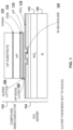
- Figure 1 illustrates the bonding of heterogeneous materials, according to some example embodiments.
- Figure 1 shows a cross-section of a compound semiconductor 102 and an SOI wafer 104 before being bonded together.
- the SOI wafer 104 or silicon-on-insulator wafer, is created with a silicon base 120, a layer of SiO 2 118 on top of the silicon base 120, and a silicon waveguide 122 that provides low-loss routing.
- a SiO 2 bonding layer 116 is added on top of the waveguide 122.
- the SOI wafer is made by forming and patterning the silicon waveguides, and then the SOI wafer is plasma cleaned.
- other layers and circuits in the SOI wafer are omitted, but a person skilled in the art would readily appreciate that the SOI wafer may include a plurality of circuits and layers.
- a compound semiconductor 102 is grown separately.
- the compound semiconductor 102 utilizes III-V type materials, a class of materials which produce efficient lasers, modulators, and detectors.
- the compound semiconductor 102 includes a base of InP substrate and additional layers are added.
- the layers include a InGaAs layer 110, another InP layer, a QWs layer 112, another InP layer 114, a super lattice 106, and an InP bond layer 108.
- a large III-V semiconductor may be formed and then singulated into a plurality of epi dies prior to bonding.
- the epi dies are referred to herein as the compound semiconductor 102, and the epi dies are bonded to the SOI wafer.
- the combination of the compound semiconductor 102 and the SOI wafer 104 is desired because the silicon provides the low-loss waveguide routing and the III-V materials provide efficient light properties. Because they are different types of materials, the compound semiconductor 102 and the SOI wafer 104 are bonded together. Different oxide types of bonding materials may be used to connect the two semiconductors together.
- the compound semiconductor 102 and the SOI wafer 104 are placed together and then pressure and heat are applied to bond them together. Afterwards, they may be plasma cleaned and further steps may be taken to form circuits on the compound semiconductor 102. That is, at this point, the silicon patterning is done, but the III-V patterning is still in progress.
- a polymer e.g., benzocyclobutene, commonly abbreviated as BCB
- BCB benzocyclobutene
- Figure 2 illustrates the damage to the compound semiconductor due to acid utilized during the processing of the bonded structure, according to some example embodiments. After the two semiconductors are bonded together, additional processing of the compound semiconductor 102 takes place. Some operations may include using acid to edge the compound semiconductor substrate 202 to reduce compound semiconductor thickness.
- the acid when using acid, the acid may edge at the bottom 204 of the compound semiconductor 102 or may create damage along the Si waveguide 122. Because there is damage 204 at the edge, the edges have to be removed, which limits how small the semiconductors may be.
- FIG. 3 illustrates the addition of a protection material via ALD 304, according to some embodiments.
- a thin film of protection material 306 is deposited using ALD 304 on the compound semiconductor 102, resulting in compound semiconductor 302 with protection material 306.
- Atomic layer deposition is a thin film deposition technique that is based on the sequential use of a gas phase chemical process. ALD is considered a type of chemical vapor deposition. A majority of ALD reactions use two chemicals, typically called precursors. These precursors react with the surface of a material one at a time in a sequential, self-limiting, manner. Through the repeated exposure to separate precursors, a thin film is slowly deposited.
- Embodiments are presented herein by using Al 2 O 3 as the protection material, but other dielectric materials may be used, such as SiO 2 , HfO 2 , ZrO 2 , SiN, TiO 2 , or other dielectric films.
- ALD is used for describing the present embodiments, but other deposition methods may be used instead, such as plasma enhanced chemical vapor deposition (PECVD), ion beam deposition (IBD), and radio frequency (RF) sputtering.
- PECVD plasma enhanced chemical vapor deposition
- IBD ion beam deposition
- RF radio frequency
- the height of the deposition layer is in the range of 1 to 50 nanometers, although other values are also possible. In some example embodiments, a 10 nm layer is utilized.
- ALD atomic layer deposition
- Figure 4 illustrates the creation of a bonded structure by bonding the compound semiconductor and the SOI wafer, according to some example embodiments.
- the compound semiconductor 302 and the SOI wafer 104 are bonded together to create a bonded structure 304.
- the two semiconductors may be bonded together by placing them together and then applying pressure and heat.
- the bond forms oxides on the III-V and oxides on the silicon, and the oxides keep the compound semiconductor 302 and the SOI wafer 104 connected.
- Figure 5 illustrates a compound structure without the super lattice, according to some example embodiments.
- a disadvantage of incorporating the Al 2 O 3 on the compound semiconductor is that the separation of the III-V from the Si waveguide is increased.
- the optical operations in the PIC need to transfer an optical mode (i.e. light) from one material to the other; therefore, reducing this separation is desirable.
- the light is routed around the chip in silicon waveguides, and then the active optical functions, such as lasers, detectors and modulators, take place in the III-V material. Therefore, in an active device, there is a coupling between the silicon and the III-V.
- the Al 2 O 3 adds thickness to the gap between the silicon and the III-V, so the performance of the coupling is decreased. The smaller the gap between the silicon and the active layer of the III-V, the better the coupling between the two materials.
- the solution is to decrease the distance of the optical coupling, such as by eliminating the super lattice in the compound semiconductor 502.
- a super lattice includes two materials which are grown one after the other in very thin layers.
- the super lattice layers may be around 10 nm while other layers may be in the tens or hundreds of nanometers.
- the purpose of the super lattice is to prevent defects from moving from the bottom surface up into the material.
- the super lattice layer acts as a defect block mechanism and improves the reliability of the device.
- the removal of the super lattice makes the compound semiconductor at risk from bond defects, yet it also improves coupling performance between the Si and compound semiconductor.
- the Al 2 O 3 layer provides similar protection by moving the bond interface away from the compound semiconductor surface, therefore some defect blocking is maintained even after removing the super lattice. Meanwhile, the distance (i.e. optical confinement) from the III-V to the silicon waveguide is reduced improving coupling performance, and the quality of the bonding is also improved. Removing the super lattice is a trade-off, but overall the performance is better with the Al 2 O 3 layer.
- the detector responsivity and modulator insertion loss were better with the 10nm Al 2 O 3 layer and without the super lattice compared to the compound semiconductor having the super lattice but no Al 2 O 3 layer.
- Figure 6 shows how the Al 2 O 3 enhanced bonded structure provides better protection during processing, according to some example embodiments.
- Figure 7 illustrates some results showing the improvement obtained by utilizing the protection layer, according to some example embodiments. A few tests were performed for semiconductors with and without Al 2 O 3 and the damage on the edges of the bond were measured.
- Capture 702 illustrates an image taken of a bonded structure without ALD Al 2 O 3
- capture 704 illustrates an image taken of a bonded structure with ALD Al 2 O 3 10 nm thick.
- Capture 702 shows that there is damage at the edge of the bonding because there is material missing, while the bonded structure with the ALD Al 2 O 3 shows no observable damage.
- the edges of the ALD Al 2 O 3 were continuous and undamaged, and there was no under-etch.
- the shear strength was also measured by checking the amount of force needed to separate the bonded structures. In some tests, the shear strength of the ALD Al 2 O 3 semiconductor was about two and a half times the shear strength of the semiconductor without the Al 2 O 3 .
- the performance of the detector regarding light responsivity was measured for different semiconductor structures. Since the super lattice had been eliminated from the compound structure, the light responsivity was improved because the Al 2 O 3 layer was thinner than the super lattice, resulting in a closer light coupling.
- Figure 8 illustrates the yield improvement gains obtained with Al 2 O 3 layer, according to some embodiments.
- the benefits of the ALD Al 2 O 3 semiconductor include: (a) reduced, or eliminated, plasma cleaning required on the III-V piece prior to bonding, which allows higher throughput; (b) smaller pieces of III-V may be bonded since the setback from III-V edge to device may be reduced; (c) reduced die size and more die per wafer, since the die size is limited currently by the III-V bond piece size; and (d) greatly reduced III-V surface defect growth after bonding.
- Device 802 is a semiconductor circuit bonded without the use of Al 2 O 3 .
- the device 802 includes four pieces of compound semiconductor 806 bonded on top of the SOI wafer. Because of the damage on the edges of the compound semiconductor 806, only a reduced portion 808 may be used for the final PIC.
- Device 804 includes four compound semiconductors 810 bonded on top of the SOI wafer. Because the compound semiconductor 810 is not damaged due to the protection provided by the Al 2 O 3 layer, the complete compound semiconductor may be utilized for the PIC.
- Figure 9 is a flowchart of a method 900 for heterogeneous integration of photonics and electronics with ALD bonding.
- the compound semiconductor material is grown, and at operation 904, the protection material is deposited on the compound semiconductor grown in operation 902.
- the deposition is performed utilizing ALD and the protection material is Al 2 O 3 , although other protection materials are also possible.
- the III-V wafer is then singulated into small pieces for bonding to the SOI wafer.
- the epi die are plasma cleaned at operation 908, ensuring that the surface is very clean before bonding.
- the SOI wafer is patterned and fabricated, including the silicon waveguides, and the SOI wafer is plasma cleaned at operation 912.
- the epi die are placed on the SOI wafer surface, and at operation 916, pressure and heat are applied to the epi die on top of the SOI wafer to improve the bond.
- the method flows to operation 918, where the epi die substrate is removed through grinding and chemical etch steps (with the improved performance provided by the protection material layer).
- additional steps are performed on the heterogeneously bonded structure for epi die and device patterning.
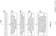
- Figure 10 is a flowchart of a method 1000 for making a bonded structure, according to some example embodiments. While the various operations in the flowcharts of Figures 9 and 10 are presented and described sequentially, one of ordinary skill will appreciate that some or all of the operations may be executed in a different order, be combined or omitted, or be executed in parallel.
- the compound semiconductor is formed (e.g., compound semiconductor 502 of Figure 5 ). From operation 1002, the method flows to operation 1004 where a continuous film of a protection material (e.g., Al 2 O 3 layer 306 of Figure 5 ) is deposited on a first surface of the compound semiconductor.
- a protection material e.g., Al 2 O 3 layer 306 of Figure 5
- a SOI wafer is formed (e.g., SOI wafer 104 of Figure 5 ), with the SOI wafer comprising one or more waveguides 122. From operation 1006, the method flows to operation 1008 for bonding the compound semiconductor at the first surface to the SOI wafer to form a bonded structure.
- the method flows to operation 1010 for processing the bonded structure.
- the protection material protects the compound semiconductor from acid etchants during the processing of the bonded structure.
- depositing the continuous film is performed by atomic layer deposition.
- the protection material is Al 2 O 3 . In other examples, the protection material is one of SiO 2 , HfO 2 , ZrO 2 , SiN, or TiO 2 .
- the continuous film has a height between 2 and 50 nanometers, but other heights of the protection layer are possible, such as in the range from 1 to 100 nanometers.
- the compound semiconductor is a III-V wafer.
- bonding the compound semiconductor to the SOI wafer further includes placing the compound semiconductor on the SOI wafer, applying pressure and heat to the compound semiconductor and the SOI wafer, and removing the pressure and heat.
- the SOI wafer includes a SiO 2 layer directly above one of the one or more waveguides, where the SiO 2 layer is placed in contact with the first surface of the compound semiconductor for the bonding.
- the compound semiconductor does not include a super lattice layer to compensate for the increased sized of the compound semiconductor with the continuous film of the protection material.
- processing the bonded structure further includes removing an epi substrate from the compound semiconductor through grind and chemical steps and device patterning on the compound semiconductor.
- the term "or" may be construed in either an inclusive or exclusive sense. Moreover, plural instances may be provided for resources, operations, or structures described herein as a single instance. Additionally, boundaries between various resources, operations, modules, engines, and data stores are somewhat arbitrary, and particular operations are illustrated in a context of specific illustrative configurations. Other allocations of functionality are envisioned and may fall within a scope of various embodiments of the present disclosure. In general, structures and functionality presented as separate resources in the example configurations may be implemented as a combined structure or resource. Similarly, structures and functionality presented as a single resource may be implemented as separate resources. These and other variations, modifications, additions, and improvements fall within a scope of embodiments of the present disclosure as represented by the appended claims. The specification and drawings are, accordingly, to be regarded in an illustrative rather than a restrictive sense.
- One method includes operations for forming a compound semiconductor and for depositing (e.g., via atomic layer deposition) a continuous film of a protection material (e.g., Al2O3) on a first surface of the compound semiconductor. Further, the method includes an operation for forming a silicon on insulator (SOI) wafer, with the SOI wafer comprising one or more waveguides. The method further includes bonding the compound semiconductor at the first surface to the SOI wafer to form a bonded structure and processing the bonded structure. The protection material protects the compound semiconductor from acid etchants during further processing of the bonded structure.
- a protection material e.g., Al2O3
Landscapes
- Physics & Mathematics (AREA)
- Engineering & Computer Science (AREA)
- Microelectronics & Electronic Packaging (AREA)
- General Physics & Mathematics (AREA)
- Optics & Photonics (AREA)
- Optical Integrated Circuits (AREA)
- Semiconductor Lasers (AREA)
Abstract
Description
- The subject matter disclosed herein generally relates to methods and systems for semiconductor manufacturing and, more specifically, to semiconductor manufacturing that includes bonding of heterogeneous materials.
- Heterogeneous bonding of two different types of materials is becoming more common in optics and electronics for manufacturing integrated circuits (IC). The combination takes advantage of using materials with specialized and different properties to be combined into a single semiconductor for processing.
- For example, a silicon on insulator (SOI) wafer provides low loss waveguide routing while a III-V compound semiconductor generates light efficiently for lasers, and absorbs light efficiently for modulators and detectors used in optical communication. The combination of these materials provides an ideal platform for creating photonic integrated circuits (PICs). Since the materials are dissimilar, the bond greatly influences the yield and process limitation in making these PICs. For example, in some applications, the goal is to make a highly integrated transmitter that is completely made through wafer-level scale processing.
- For hybrid Si photonics, the shear strength of the bond between the compound semiconductor to the Si substrate has a great impact of device yield. Since the materials being bonded are different, separation and delamination between the materials is a common challenge to overcome. In addition, a multitude of acids are used in the fabrication of these devices to etch the compound semiconductor after bonding. However, the acids wick underneath the compound semiconductor following the Si channels and etch the bonding interface.
- Various ones of the appended drawings merely illustrate example embodiments of the present disclosure and cannot be considered as limiting its scope.
-
Figure 1 illustrates the bonding of heterogeneous materials, according to some example embodiments. -
Figure 2 illustrates the damage to the compound semiconductor due to acid utilized during the processing of the bonded structure, according to some example embodiments. -
Figure 3 illustrates the addition of a protection material via atomic layer deposition (ALD), according to some embodiments. -
Figure 4 illustrates the creation of a bonded structure by bonding the compound semiconductor and the SOI wafer, according to some example embodiments. -
Figure 5 illustrates a compound structure without a super lattice, according to some example embodiments. -
Figure 6 shows how the Al2O3 enhanced bonded structure provides better protection during processing, according to some example embodiments. -
Figure 7 illustrates some results showing the improvement obtained by utilizing the protection layer, according to some example embodiments. -
Figure 8 illustrates the yield improvement gains obtained with the Al2O3 layer, according to some embodiments. -
Figure 9 is a flowchart of a method for heterogeneous integration of photonics and electronics with ALD bonding. -
Figure 10 is a flowchart of a method for making a bonded structure, according to some example embodiments. - Example methods and systems are directed to for heterogeneous integration of photonics and electronics with atomic layer deposition (ALD) bonding. Examples merely typify possible variations. Unless explicitly stated otherwise, components and functions are optional and may be combined or subdivided, and operations may vary in sequence or be combined or subdivided. In the following description, for purposes of explanation, numerous specific details are set forth to provide a thorough understanding of example embodiments. It will be evident to one skilled in the art, however, that the present subject matter may be practiced without these specific in details.
- The bonded structure has problems that must be addressed during manufacturing, such as the bonding shear strength and acid damage in post-bonding processing. Some solutions solve these problems by changing the bond layer of the III-V semiconductor to InGaAsP, which is more resistant to many acid etches. However, this change also reduces the shear strength and leads to delamination prior to the acid steps. Other solutions include changes to the acid etch steps, the device artwork, or the setback from the III-V edge to the III-V devices. However, these solutions do not increase the shear strength of the bonding, they add processing time and cost, and they do not fully solve the problem of acid wicking. Further, these solutions do not allow the setback from the III-V edge to the device to be reduced, thereby limiting the shrinking of the die size.
- Embodiments presented herein provide solutions for bonding an SOI wafer with a compound semiconductor (e.g., a semiconductor formed on III-V materials). Embodiments provide for adding a thin layer of protection material (e.g., Al2O3) to the bonding surface in the compound semiconductor (e.g., III-V based) after growth and prior to the bonding operation. In some examples, the addition of the thin layer is performed via ALD, but other deposition methods may be utilized. The Al2O3 protects the III-V material from acid etchants after bonding and also increases the shear strength of the bond (e.g., compared to SiO2). In addition, the protection material results in fewer defects, higher yields, and provides the ability to make smaller optical circuits while using less material.
- One general aspect includes a method including operations for forming a compound semiconductor, depositing a continuous film of a protection material on a first surface of the compound semiconductor, and forming a SOI wafer, with the SOI wafer including one or more waveguides. The method also includes bonding the compound semiconductor at the first surface to the SOI wafer to form a bonded structure and processing the bonded structure. The protection material protects the compound semiconductor from acid etchants during the processing of the bonded structure.
- One general aspect includes a bonded structure including a compound semiconductor, including a continuous film of a protection material deposited on a first surface of the compound semiconductor, and a SOI wafer. The SOI wafer includes one or more waveguides, where the compound semiconductor is bonded at the first surface to the SOI wafer to form the semiconductor structure, the bonded structure being processable to pattern circuits on the compound semiconductor. The protection material protects the compound semiconductor from acid etchants during the processing of the bonded structure.
- One general aspect includes a method including operations for forming a III-V based semiconductor, depositing a continuous film of Al2O3 on a first surface of the III-V based semiconductor, singulating the III-V based semiconductor to create epi dies, and plasma cleaning the epi dies. The method further includes operations for forming a SOI wafer, with the SOI wafer including one or more waveguides, placing the first surface of the epi dies on the SOI wafer, bonding the epi dies to the SOI wafer to form a bonded structure, removing a substrate of the epi die through grind and chemical operations, and processing the bonded structure, where the Al2O3 protects the epi dies from acid etchants during the processing of the bonded structure.
-
Figure 1 illustrates the bonding of heterogeneous materials, according to some example embodiments.Figure 1 shows a cross-section of acompound semiconductor 102 and anSOI wafer 104 before being bonded together. The SOI wafer 104, or silicon-on-insulator wafer, is created with asilicon base 120, a layer of SiO2 118 on top of thesilicon base 120, and asilicon waveguide 122 that provides low-loss routing. In addition, a SiO2 bonding layer 116 is added on top of thewaveguide 122. The SOI wafer is made by forming and patterning the silicon waveguides, and then the SOI wafer is plasma cleaned. For simplicity of description, other layers and circuits in the SOI wafer are omitted, but a person skilled in the art would readily appreciate that the SOI wafer may include a plurality of circuits and layers. - Further, a
compound semiconductor 102 is grown separately. In some example embodiments, thecompound semiconductor 102 utilizes III-V type materials, a class of materials which produce efficient lasers, modulators, and detectors. - In some example embodiments, the
compound semiconductor 102 includes a base of InP substrate and additional layers are added. In the example embodiment ofFigure 1 , the layers include aInGaAs layer 110, another InP layer, aQWs layer 112, anotherInP layer 114, asuper lattice 106, and anInP bond layer 108. - It is noted that a large III-V semiconductor may be formed and then singulated into a plurality of epi dies prior to bonding. The epi dies are referred to herein as the
compound semiconductor 102, and the epi dies are bonded to the SOI wafer. - The combination of the
compound semiconductor 102 and theSOI wafer 104 is desired because the silicon provides the low-loss waveguide routing and the III-V materials provide efficient light properties. Because they are different types of materials, thecompound semiconductor 102 and theSOI wafer 104 are bonded together. Different oxide types of bonding materials may be used to connect the two semiconductors together. - In some example embodiments, the
compound semiconductor 102 and theSOI wafer 104 are placed together and then pressure and heat are applied to bond them together. Afterwards, they may be plasma cleaned and further steps may be taken to form circuits on thecompound semiconductor 102. That is, at this point, the silicon patterning is done, but the III-V patterning is still in progress. In other bonding approaches, a polymer (e.g., benzocyclobutene, commonly abbreviated as BCB) bond is used, such that the III-V is connected to the silicon using the polymer. - It is noted that the embodiments illustrated in
Figure 1 are examples and do not describe every possible embodiment. Other embodiments may utilize different, additional, or fewer layers on thecompound semiconductor 102 and theSOI wafer 104. The embodiments illustrated inFigure 1 should therefore not be interpreted to be exclusive or limiting, but rather illustrative. -
Figure 2 illustrates the damage to the compound semiconductor due to acid utilized during the processing of the bonded structure, according to some example embodiments. After the two semiconductors are bonded together, additional processing of thecompound semiconductor 102 takes place. Some operations may include using acid to edge thecompound semiconductor substrate 202 to reduce compound semiconductor thickness. - However, when using acid, the acid may edge at the bottom 204 of the
compound semiconductor 102 or may create damage along theSi waveguide 122. Because there isdamage 204 at the edge, the edges have to be removed, which limits how small the semiconductors may be. -
Figure 3 illustrates the addition of a protection material viaALD 304, according to some embodiments. In some example embodiments, a thin film ofprotection material 306 is deposited usingALD 304 on thecompound semiconductor 102, resulting incompound semiconductor 302 withprotection material 306. Atomic layer deposition (ALD) is a thin film deposition technique that is based on the sequential use of a gas phase chemical process. ALD is considered a type of chemical vapor deposition. A majority of ALD reactions use two chemicals, typically called precursors. These precursors react with the surface of a material one at a time in a sequential, self-limiting, manner. Through the repeated exposure to separate precursors, a thin film is slowly deposited. - Embodiments are presented herein by using Al2O3 as the protection material, but other dielectric materials may be used, such as SiO2, HfO2, ZrO2, SiN, TiO2, or other dielectric films. In addition, ALD is used for describing the present embodiments, but other deposition methods may be used instead, such as plasma enhanced chemical vapor deposition (PECVD), ion beam deposition (IBD), and radio frequency (RF) sputtering.
- The height of the deposition layer is in the range of 1 to 50 nanometers, although other values are also possible. In some example embodiments, a 10 nm layer is utilized.
- One of the advantages of using ALD is that it improves the shear strength of the bond because, among other reasons, it provides a virtually defect free layer that is better suited for bonding. The ALD films are completely conformal in that there are no breaks in the films and no discontinuities. It is also easy to control the thickness of the film so that the layer may be as small as a single monolayer (approximately a nanometer) and all the way up to tens or hundreds of nanometers. The results from using Al2O3 deposited with ALD is that the bond quality is greatly improved.
-
Figure 4 illustrates the creation of a bonded structure by bonding the compound semiconductor and the SOI wafer, according to some example embodiments. After the Al2O3 is deposited, thecompound semiconductor 302 and theSOI wafer 104 are bonded together to create a bondedstructure 304. For example, the two semiconductors may be bonded together by placing them together and then applying pressure and heat. - The bond forms oxides on the III-V and oxides on the silicon, and the oxides keep the
compound semiconductor 302 and theSOI wafer 104 connected. -
Figure 5 illustrates a compound structure without the super lattice, according to some example embodiments. A disadvantage of incorporating the Al2O3 on the compound semiconductor is that the separation of the III-V from the Si waveguide is increased. The optical operations in the PIC need to transfer an optical mode (i.e. light) from one material to the other; therefore, reducing this separation is desirable. - In the photonic integrated circuits, the light is routed around the chip in silicon waveguides, and then the active optical functions, such as lasers, detectors and modulators, take place in the III-V material. Therefore, in an active device, there is a coupling between the silicon and the III-V. The Al2O3 adds thickness to the gap between the silicon and the III-V, so the performance of the coupling is decreased. The smaller the gap between the silicon and the active layer of the III-V, the better the coupling between the two materials.
- In some example embodiments, the solution is to decrease the distance of the optical coupling, such as by eliminating the super lattice in the
compound semiconductor 502. A super lattice includes two materials which are grown one after the other in very thin layers. For example, the super lattice layers may be around 10 nm while other layers may be in the tens or hundreds of nanometers. The purpose of the super lattice is to prevent defects from moving from the bottom surface up into the material. The super lattice layer acts as a defect block mechanism and improves the reliability of the device. The removal of the super lattice makes the compound semiconductor at risk from bond defects, yet it also improves coupling performance between the Si and compound semiconductor. - However, the Al2O3 layer provides similar protection by moving the bond interface away from the compound semiconductor surface, therefore some defect blocking is maintained even after removing the super lattice. Meanwhile, the distance (i.e. optical confinement) from the III-V to the silicon waveguide is reduced improving coupling performance, and the quality of the bonding is also improved. Removing the super lattice is a trade-off, but overall the performance is better with the Al2O3 layer.
- In simulations, the detector responsivity and modulator insertion loss were better with the 10nm Al2O3 layer and without the super lattice compared to the compound semiconductor having the super lattice but no Al2O3 layer.
-
Figure 6 shows how the Al2O3 enhanced bonded structure provides better protection during processing, according to some example embodiments. After adding the Al2O3 306 to thecompound structure 502, it was observed that the damage from acid utilized during etching 602 operations was greatly reduced. The damage was reduced on the edges of the compound semiconductor as well as along the silicon waveguide. - In some laboratory tests, and cited as an example without meaning to be limiting, the observed damage at the edges with a 10 nm layer of Al2O3 were practically eliminated. At 2 nm and at 5 nm some damage at the edge was observed, but the damage was less than without using the Al2O3 layer. Further, the shear strength of the bonding was also improved. More sample results are provided below with reference to
Figure 7 . -
Figure 7 illustrates some results showing the improvement obtained by utilizing the protection layer, according to some example embodiments. A few tests were performed for semiconductors with and without Al2O3 and the damage on the edges of the bond were measured. -
Capture 702 illustrates an image taken of a bonded structure without ALD Al2O3, and capture 704 illustrates an image taken of a bonded structure with ALD Al2O3 10 nm thick. Capture 702 shows that there is damage at the edge of the bonding because there is material missing, while the bonded structure with the ALD Al2O3 shows no observable damage. The edges of the ALD Al2O3 were continuous and undamaged, and there was no under-etch. - The shear strength was also measured by checking the amount of force needed to separate the bonded structures. In some tests, the shear strength of the ALD Al2O3 semiconductor was about two and a half times the shear strength of the semiconductor without the Al2O3.
- In other tests, the performance of the detector regarding light responsivity was measured for different semiconductor structures. Since the super lattice had been eliminated from the compound structure, the light responsivity was improved because the Al2O3 layer was thinner than the super lattice, resulting in a closer light coupling.
-
Figure 8 illustrates the yield improvement gains obtained with Al2O3 layer, according to some embodiments. The benefits of the ALD Al2O3 semiconductor include: (a) reduced, or eliminated, plasma cleaning required on the III-V piece prior to bonding, which allows higher throughput; (b) smaller pieces of III-V may be bonded since the setback from III-V edge to device may be reduced; (c) reduced die size and more die per wafer, since the die size is limited currently by the III-V bond piece size; and (d) greatly reduced III-V surface defect growth after bonding. -
Device 802 is a semiconductor circuit bonded without the use of Al2O3. Thedevice 802 includes four pieces ofcompound semiconductor 806 bonded on top of the SOI wafer. Because of the damage on the edges of thecompound semiconductor 806, only a reduced portion 808 may be used for the final PIC. -
Device 804 includes fourcompound semiconductors 810 bonded on top of the SOI wafer. Because thecompound semiconductor 810 is not damaged due to the protection provided by the Al2O3 layer, the complete compound semiconductor may be utilized for the PIC. - It is also noted that because the compound semiconductors are not damaged, it is possible to place the III-V pieces closer together, which results in smaller PICs and improved III-V usage, resulting in less waste and less cost for the III-V semiconductor. Further, since there is less waste on the III-V semiconductor, there is also less waste on the SOI wafer, resulting in reduced silicon expenses.
- In some examples, it is possible to use simpler manufacturing processes because the compound semiconductor is not as sensitive to acid chemicals.
-
Figure 9 is a flowchart of amethod 900 for heterogeneous integration of photonics and electronics with ALD bonding. Atoperation 902, the compound semiconductor material is grown, and atoperation 904, the protection material is deposited on the compound semiconductor grown inoperation 902. In some example embodiments, the deposition is performed utilizing ALD and the protection material is Al2O3, although other protection materials are also possible. - At
operation 906, the III-V wafer is then singulated into small pieces for bonding to the SOI wafer. The epi die are plasma cleaned atoperation 908, ensuring that the surface is very clean before bonding. - At
operation 910, the SOI wafer is patterned and fabricated, including the silicon waveguides, and the SOI wafer is plasma cleaned atoperation 912. - At
operation 914, the epi die are placed on the SOI wafer surface, and atoperation 916, pressure and heat are applied to the epi die on top of the SOI wafer to improve the bond. - From
operation 916, the method flows tooperation 918, where the epi die substrate is removed through grinding and chemical etch steps (with the improved performance provided by the protection material layer). Atoperation 920, additional steps are performed on the heterogeneously bonded structure for epi die and device patterning. -
Figure 10 is a flowchart of amethod 1000 for making a bonded structure, according to some example embodiments. While the various operations in the flowcharts ofFigures 9 and10 are presented and described sequentially, one of ordinary skill will appreciate that some or all of the operations may be executed in a different order, be combined or omitted, or be executed in parallel. - At
operation 1002, the compound semiconductor is formed (e.g.,compound semiconductor 502 ofFigure 5 ). Fromoperation 1002, the method flows to operation 1004 where a continuous film of a protection material (e.g., Al2O3 layer 306 ofFigure 5 ) is deposited on a first surface of the compound semiconductor. - Further, at
operation 1006, a SOI wafer is formed (e.g.,SOI wafer 104 ofFigure 5 ), with the SOI wafer comprising one ormore waveguides 122. Fromoperation 1006, the method flows tooperation 1008 for bonding the compound semiconductor at the first surface to the SOI wafer to form a bonded structure. - From
operation 1008, the method flows tooperation 1010 for processing the bonded structure. The protection material protects the compound semiconductor from acid etchants during the processing of the bonded structure. - In one example, depositing the continuous film is performed by atomic layer deposition.
- In some examples, the protection material is Al2O3. In other examples, the protection material is one of SiO2, HfO2, ZrO2, SiN, or TiO2.
- In some examples, the continuous film has a height between 2 and 50 nanometers, but other heights of the protection layer are possible, such as in the range from 1 to 100 nanometers.
- In some example embodiments, the compound semiconductor is a III-V wafer.
- In some example embodiments, bonding the compound semiconductor to the SOI wafer further includes placing the compound semiconductor on the SOI wafer, applying pressure and heat to the compound semiconductor and the SOI wafer, and removing the pressure and heat.
- In some examples, the SOI wafer includes a SiO2 layer directly above one of the one or more waveguides, where the SiO2 layer is placed in contact with the first surface of the compound semiconductor for the bonding.
- In some examples, the compound semiconductor does not include a super lattice layer to compensate for the increased sized of the compound semiconductor with the continuous film of the protection material.
- In some examples, processing the bonded structure further includes removing an epi substrate from the compound semiconductor through grind and chemical steps and device patterning on the compound semiconductor.
- Throughout this specification, plural instances may implement components, operations, or structures described as a single instance. Although individual operations of one or more methods are illustrated and described as separate operations, one or more of the individual operations may be performed concurrently, and nothing requires that the operations be performed in the order illustrated. Structures and functionality presented as separate components in example configurations may be implemented as a combined structure or component. Similarly, structures and functionality presented as a single component may be implemented as separate components. These and other variations, modifications, additions, and improvements fall within the scope of the subject matter herein.
- The embodiments illustrated herein are described in sufficient detail to enable those skilled in the art to practice the teachings disclosed. Other embodiments may be used and derived therefrom, such that structural and logical substitutions and changes may be made without departing from the scope of this disclosure. The Detailed Description, therefore, is not to be taken in a limiting sense, and the scope of various embodiments is defined only by the appended claims, along with the full range of equivalents to which such claims are entitled.
- As used herein, the term "or" may be construed in either an inclusive or exclusive sense. Moreover, plural instances may be provided for resources, operations, or structures described herein as a single instance. Additionally, boundaries between various resources, operations, modules, engines, and data stores are somewhat arbitrary, and particular operations are illustrated in a context of specific illustrative configurations. Other allocations of functionality are envisioned and may fall within a scope of various embodiments of the present disclosure. In general, structures and functionality presented as separate resources in the example configurations may be implemented as a combined structure or resource. Similarly, structures and functionality presented as a single resource may be implemented as separate resources. These and other variations, modifications, additions, and improvements fall within a scope of embodiments of the present disclosure as represented by the appended claims. The specification and drawings are, accordingly, to be regarded in an illustrative rather than a restrictive sense.
- Thus, from one perspective, there have now been described methods and systems for heterogeneous integration of photonics and electronics with atomic layer deposition (ALD) bonding. One method includes operations for forming a compound semiconductor and for depositing (e.g., via atomic layer deposition) a continuous film of a protection material (e.g., Al2O3) on a first surface of the compound semiconductor. Further, the method includes an operation for forming a silicon on insulator (SOI) wafer, with the SOI wafer comprising one or more waveguides. The method further includes bonding the compound semiconductor at the first surface to the SOI wafer to form a bonded structure and processing the bonded structure. The protection material protects the compound semiconductor from acid etchants during further processing of the bonded structure.
- Example aspects of the present disclosure are presented in the following numbered clauses:
- 1. A method comprising:
- forming a compound semiconductor;
- depositing a continuous film of a protection material on a first surface of the compound semiconductor;
- forming a silicon on insulator (SOI) wafer, the SOI wafer comprising one or more waveguides;
- bonding the compound semiconductor at the first surface to the SOI wafer to form a bonded structure; and
- processing the bonded structure, the protection material protecting the compound semiconductor from acid etchants during the processing of the bonded structure.
- 2. The method as recited in clause 1, wherein the depositing the continuous film is performed by atomic layer deposition.
- 3. The method as recited in clause 1 or clause 2, wherein the protection material is Al2O3.
- 4. The method as recited in any preceding clause, wherein the protection material is one of SiO2, HfO2, ZrO2, SiN, or TiO2.
- 5. The method as recited in any preceding clause, wherein the continuous film has a height between 2 and 50 nanometers.
- 6. The method as recited in any preceding clause, wherein the compound semiconductor is a III-V wafer.
- 7. The method as recited in any preceding clause, wherein bonding the compound semiconductor to the SOI wafer further comprises:
- placing the compound semiconductor on the SOI wafer;
- applying pressure and heat to the compound semiconductor and the SOI wafer; and
- removing the pressure and heat.
- 8. The method as recited in any preceding clause, wherein the SOI wafer includes a SiO2 layer directly above one of the one or more waveguides, wherein the SiO2 layer is placed in contact with the first surface of the compound semiconductor for the bonding.
- 9. The method as recited in any preceding clause, wherein the compound semiconductor does not include a super lattice layer to compensate for the increased sized of the compound semiconductor with the continuous film of the protection material.
- 10. The method as recited in any preceding clause, wherein processing the bonded structure further comprises:
- removing an epi substrate from the compound semiconductor through grind and chemical steps; and
- device patterning on the compound semiconductor.
- 11. A bonded structure comprising:
- a compound semiconductor comprising a continuous film of a protection material deposited on a first surface of the compound semiconductor; and
- a silicon on insulator (SOI) wafer, the SOI wafer comprising one or more waveguides, wherein the compound semiconductor is bonded at the first surface to the SOI wafer to form the semiconductor structure, wherein the bonded structure is processable to pattern circuits on the compound semiconductor, the protection material protecting the compound semiconductor from acid etchants during the processing of the bonded structure.
- 12. The bonded structure as recited in clause 11, wherein the protection material is Al2O3.
- 13. The bonded structure as recited in clause 11 or clause 12, wherein the protection material is one of SiO2, HfO2, ZrO2, SiN, or TiO2.
- 14. The bonded structure as recited in any of clauses 11 to 13, wherein the continuous film has a height between 2 and 50 nanometers.
- 15. The bonded structure as recited in any of clauses 11 to 14, wherein the compound semiconductor is a III-V wafer.
- 16. The bonded structure as recited in any of clauses 11 to 15, wherein the SOI wafer includes a SiO2 layer directly above one of the one or more waveguides, wherein the SiO2 layer is placed in contact with the first surface of the compound semiconductor for the bonding.
- 17. A method comprising:
- forming a III-V based semiconductor;
- depositing a continuous film of Al2O3 on a first surface of the III-V based semiconductor;
- singulating the III-V based semiconductor to create epi dies;
- plasma cleaning the epi dies;
- forming a silicon on insulator (SOI) wafer, the SOI wafer comprising one or more waveguides;
- placing the first surfaces of the epi dies on the SOI wafer;
- bonding the epi dies to the SOI wafer to form a bonded structure;
- removing a substrate of the epi die through grind and chemical operations; and
- processing the bonded structure, the Al2O3 protecting the epi dies from acid etchants during the processing of the bonded structure.
- 18. The method as recited in clause 17, wherein depositing the continuous film is performed by atomic layer deposition.
- 19. The method as recited in clause 17 or clause 18, wherein bonding the epi dies to the SOI wafer further comprises:
- applying pressure and heat to the epi dies and the SOI wafer; and
- removing the pressure and heat.
- 20. The method as recited in any of clauses 17 to 19, wherein the SOI wafer includes a SiO2 layer directly above one of the one or more waveguides, wherein the SiO2 layer is placed in contact with the first surface of the compound semiconductor for the bonding.
-
- 1. A method comprising:
- forming a compound semiconductor;
- depositing a continuous film of a protection material on a first surface of the compound semiconductor;
- forming a silicon on insulator (SOI) wafer, the SOI wafer comprising one or more waveguides;
- bonding the compound semiconductor at the first surface to the SOI wafer to form a bonded structure; and
- processing the bonded structure, the protection material protecting the compound semiconductor from acid etchants during the processing of the bonded structure.
- 2. The method as recited in clause 1, wherein the depositing the continuous film is performed by atomic layer deposition.
- 3. The method as recited in clause 1 or clause 2, wherein the protection material is Al2O3.
- 4. The method as recited in clause 1 or clause 2, wherein the protection material is one of SiO2 HfO2, ZrO2, SiN, or TiO2.
- 5. The method as recited in any preceding clause, wherein the continuous film has a height between 2 and 50 nanometers.
- 6. The method as recited in any preceding clause, wherein the compound semiconductor is a III-V wafer.
- 7. The method as recited in any preceding clause, wherein bonding the compound semiconductor to the SOI wafer further comprises:
- placing the compound semiconductor on the SOI wafer;
- applying pressure and heat to the compound semiconductor and the SOI wafer; and
- removing the pressure and heat.
- 8. The method as recited in any preceding clause, wherein the SOI wafer includes a SiOz layer directly above one of the one or more waveguides, wherein the SiO2 layer is placed in contact with the first surface of the compound semiconductor for the bonding.
- 9. The method as recited in any preceding clause, wherein the compound semiconductor does not include a super lattice layer to compensate for the increased sized of the compound semiconductor with the continuous film of the protection material.
- 10. The method as recited in any preceding clause, wherein processing the bonded structure further comprises:
- removing an epi substrate from the compound semiconductor through grind and chemical steps; and
- device patterning on the compound semiconductor.
- 11. A bonded structure comprising:
- a compound semiconductor comprising a continuous film of a protection material deposited on a first surface of the compound semiconductor; and
- a silicon on insulator (SOI) wafer, the SOI wafer comprising one or more waveguides, wherein the compound semiconductor is bonded at the first surface to the SOI wafer to form the semiconductor structure, wherein the bonded structure is processable to pattern circuits on the compound semiconductor, the protection material protecting the compound semiconductor from acid etchants during the processing of the bonded structure.
- 12. The bonded structure as recited in clause 11, wherein the protection material is one of Al2O3, SiO2, HfO2, ZrO2, SiN, or TiO2.
- 13. The bonded structure as recited in clause 11 or clause 12, wherein the continuous film has a height between 2 and 50 nanometers.
- 14. The bonded structure as recited in any of clauses 11-13, wherein the compound semiconductor is a III-V wafer.
- 15. The bonded structure as recited in any of clauses 11-14, wherein the SOI wafer includes a SiO2 layer directly above one of the one or more waveguides, wherein the SiO2 layer is placed in contact with the first surface of the compound semiconductor for the bonding.
Claims (15)
- A photonic integrated circuit comprising:a compound semiconductor comprising a film of a first oxide material deposited on a first side of the compound semiconductor, wherein the first oxide material is at least one as follows: Al2O3, SiO2, HfO2, ZrO2, SiN, TiO2, or other dielectric; anda silicon on insulator (SOI) wafer comprising one or more waveguides and a layer of a second oxide material on a second side of the SOI wafer, the first oxide material and the second oxide material being different types of oxide materials, wherein the first side of the compound semiconductor is bonded to the second side of the SOI wafer such that the film of the first oxide material is in contact with the layer of the second oxide material of the SOI wafer.
- The photonic integrated circuit as recited in claim 1, wherein the compound semiconductor comprises a circuit patterned on the compound semiconductor using etchants, the film of the first oxide material protecting the first side of the compound semiconductor from the etchants.
- The photonic integrated circuit as recited in claim 2, wherein the film of the first oxide material further protects the second side of the SOI wafer from the etchants.
- The photonic integrated circuit of as recited in claim 1, wherein the film of the first oxide material is a atomic layer deposited thin film or a PECVD thin film.
- The photonic integrated circuit as recited in claim 4, wherein the vapor deposited thin film is a continuous film with no discontinuities.
- The photonic integrated circuit as recited in claim 1, wherein the film has a height between 2 and 50 nanometers.
- The photonic integrated circuit as recited in claim 1, wherein the compound semiconductor is a III-V wafer.
- The photonic integrated circuit as recited in claim 1, wherein the layer of the second oxide material is a silicon oxide layer directly above one of the one or more waveguides, wherein the silicon oxide layer is placed in contact with the first side of the compound semiconductor.
- The photonic integrated circuit as recited in claim 1, wherein the compound semiconductor is bonded to the SOI wafer using heat and pressure.
- The photonic integrated circuit as recited in claim 1, wherein the compound semiconductor is a die from a plurality of dies singulated from a III-V wafer.
- The photonic integrated circuit as recited in claim 1, wherein the first oxide material is aluminum oxide.
- The photonic integrated circuit as recited in claim 1, wherein the second oxide material is silicon oxide.
- The photonic integrated circuit as recited in claim 1, wherein the compound semiconductor does not include a super lattice layer to compensate for increased sized of the compound semiconductor with the film of the first oxide material.
- A photonic circuit comprising:a compound semiconductor comprising a continuous film of a first oxide material deposited on a first side of the compound semiconductor, the compound semiconductor being a die from a plurality of dies singulated a III-V wafer, wherein the first oxide material is at least one as follows: Al2O3, SiO2, HfO2, ZrO2, SiN, TiO2, or other dielectric; anda silicon on insulator (SOI) wafer comprising one or more waveguides and a layer of a second oxide material on a second side of the SOI wafer, the first oxide material and the second oxide material being different types of oxide materials, wherein the first side of the compound semiconductor is bonded to the second side of the SOI wafer such that the continuous film of the first oxide material is in contact with the layer of the second oxide material of the SOI wafer.
- The photonic circuit as recited in claim 14, wherein the compound semiconductor comprises a circuit patterned in the compound semiconductor using etchants, the film of the first oxide material protecting the first side of the compound semiconductor from the etchants.
Applications Claiming Priority (2)
| Application Number | Priority Date | Filing Date | Title |
|---|---|---|---|
| US15/408,725 US10168475B2 (en) | 2017-01-18 | 2017-01-18 | Atomic layer deposition bonding for heterogeneous integration of photonics and electronics |
| EP18151086.8A EP3352208B1 (en) | 2017-01-18 | 2018-01-10 | Atomic layer deposition bonding for heterogeneous integration of photonics and electronics |
Related Parent Applications (2)
| Application Number | Title | Priority Date | Filing Date |
|---|---|---|---|
| EP18151086.8A Division-Into EP3352208B1 (en) | 2017-01-18 | 2018-01-10 | Atomic layer deposition bonding for heterogeneous integration of photonics and electronics |
| EP18151086.8A Division EP3352208B1 (en) | 2017-01-18 | 2018-01-10 | Atomic layer deposition bonding for heterogeneous integration of photonics and electronics |
Publications (1)
| Publication Number | Publication Date |
|---|---|
| EP4216261A1 true EP4216261A1 (en) | 2023-07-26 |
Family
ID=60972033
Family Applications (2)
| Application Number | Title | Priority Date | Filing Date |
|---|---|---|---|
| EP23162640.9A Pending EP4216261A1 (en) | 2017-01-18 | 2018-01-10 | Atomic layer deposition bonding for heterogeneous integration of photonics and electronics |
| EP18151086.8A Active EP3352208B1 (en) | 2017-01-18 | 2018-01-10 | Atomic layer deposition bonding for heterogeneous integration of photonics and electronics |
Family Applications After (1)
| Application Number | Title | Priority Date | Filing Date |
|---|---|---|---|
| EP18151086.8A Active EP3352208B1 (en) | 2017-01-18 | 2018-01-10 | Atomic layer deposition bonding for heterogeneous integration of photonics and electronics |
Country Status (3)
| Country | Link |
|---|---|
| US (4) | US10168475B2 (en) |
| EP (2) | EP4216261A1 (en) |
| CN (1) | CN108335971B (en) |
Families Citing this family (12)
| Publication number | Priority date | Publication date | Assignee | Title |
|---|---|---|---|---|
| US10168475B2 (en) | 2017-01-18 | 2019-01-01 | Juniper Networks, Inc. | Atomic layer deposition bonding for heterogeneous integration of photonics and electronics |
| US10768365B2 (en) * | 2018-03-21 | 2020-09-08 | Futurewei Technologies, Inc. | Enabling thermal efficiency on a silicon-on-insulator (SOI) platform |
| JP7159750B2 (en) * | 2018-09-26 | 2022-10-25 | 住友電気工業株式会社 | OPTO-SEMICONDUCTOR DEVICE AND MANUFACTURING METHOD THEREOF |
| JP2020155715A (en) * | 2019-03-22 | 2020-09-24 | 住友電気工業株式会社 | Optical semiconductor devices and their manufacturing methods |
| CN112285827B (en) * | 2020-09-30 | 2022-10-04 | 中国科学院微电子研究所 | Preparation method of multilayer silicon photonic device |
| WO2022073604A1 (en) * | 2020-10-07 | 2022-04-14 | Huawei Technologies Co., Ltd. | Forming semiconductor devices for non-hermetic environments |
| US11914264B2 (en) * | 2020-10-07 | 2024-02-27 | Openlight Photonics, Inc. | Hybrid photonic ring modulators |
| CN114032527A (en) * | 2021-09-16 | 2022-02-11 | 重庆康佳光电技术研究院有限公司 | Method for preparing passivation layer of epitaxial wafer, light-emitting chip and display device |
| WO2023249564A1 (en) * | 2022-06-23 | 2023-12-28 | National University Of Singapore | A waveguide-integrated avalanche photodiode |
| CN115863472A (en) * | 2022-11-17 | 2023-03-28 | 西安电子科技大学重庆集成电路创新研究院 | A gallium nitride-based avalanche photodetector that can be integrated on a chip and its preparation method |
| US20250079357A1 (en) * | 2023-09-01 | 2025-03-06 | Applied Materials, Inc. | Methods and structures for high strength asymmetric dielectric in hybrid bonding |
| US20250370202A1 (en) * | 2024-06-03 | 2025-12-04 | Celestial Ai Inc. | Packaging optical components in a circuit package |
Citations (1)
| Publication number | Priority date | Publication date | Assignee | Title |
|---|---|---|---|---|
| EP2720327A1 (en) * | 2012-10-10 | 2014-04-16 | Samsung Electronics Co., Ltd | Hybrid vertical cavity laser for photonic integrated circuit |
Family Cites Families (82)
| Publication number | Priority date | Publication date | Assignee | Title |
|---|---|---|---|---|
| US5263111A (en) * | 1991-04-15 | 1993-11-16 | Raychem Corporation | Optical waveguide structures and formation methods |
| US5394490A (en) * | 1992-08-11 | 1995-02-28 | Hitachi, Ltd. | Semiconductor device having an optical waveguide interposed in the space between electrode members |
| JP3751052B2 (en) * | 1994-12-28 | 2006-03-01 | シャープ株式会社 | Integrated light control element and method for manufacturing the same, and optical integrated circuit element and optical integrated circuit device including the same |
| US6282219B1 (en) * | 1998-08-12 | 2001-08-28 | Texas Instruments Incorporated | Substrate stack construction for enhanced coupling efficiency of optical couplers |
| US6684007B2 (en) * | 1998-10-09 | 2004-01-27 | Fujitsu Limited | Optical coupling structures and the fabrication processes |
| US6324313B1 (en) * | 1998-12-21 | 2001-11-27 | Lsi Logic Corporation | On-chip multiple layer vertically transitioning optical waveguide and damascene method of fabricating the same |
| US6984571B1 (en) | 1999-10-01 | 2006-01-10 | Ziptronix, Inc. | Three dimensional device integration method and integrated device |
| US6500694B1 (en) | 2000-03-22 | 2002-12-31 | Ziptronix, Inc. | Three dimensional device integration method and integrated device |
| AU1794101A (en) * | 1999-11-23 | 2001-06-04 | Nanovation Technologies, Inc. | Optical mach-zehnder switch with movable phase shifter |
| US6614947B1 (en) * | 1999-11-23 | 2003-09-02 | Lnl Technologies, Inc. | Digital optical switch using an integrated mach-zehnder interferometer having a movable phase shifter |
| JP3975634B2 (en) * | 2000-01-25 | 2007-09-12 | 信越半導体株式会社 | Manufacturing method of semiconductor wafer |
| US6902987B1 (en) | 2000-02-16 | 2005-06-07 | Ziptronix, Inc. | Method for low temperature bonding and bonded structure |
| US7123794B2 (en) * | 2000-03-16 | 2006-10-17 | Lightsmyth Technologies Inc | Distributed optical structures designed by computed interference between simulated optical signals |
| US7027475B1 (en) * | 2000-04-11 | 2006-04-11 | Nuvonyx, Inc. | Tailored index single mode optical amplifiers and devices and systems including same |
| KR100401655B1 (en) | 2001-01-18 | 2003-10-17 | 주식회사 컴텍스 | A smart process with alumina dielectric layer formation using ALE and a manufacturing method of unibond type SOI wafer |
| US6912330B2 (en) * | 2001-05-17 | 2005-06-28 | Sioptical Inc. | Integrated optical/electronic circuits and associated methods of simultaneous generation thereof |
| US7116851B2 (en) * | 2001-10-09 | 2006-10-03 | Infinera Corporation | Optical signal receiver, an associated photonic integrated circuit (RxPIC), and method improving performance |
| US6801679B2 (en) * | 2001-11-23 | 2004-10-05 | Seungug Koh | Multifunctional intelligent optical modules based on planar lightwave circuits |
| US6640021B2 (en) * | 2001-12-11 | 2003-10-28 | International Business Machines Corporation | Fabrication of a hybrid integrated circuit device including an optoelectronic chip |
| US6934455B2 (en) * | 2002-12-24 | 2005-08-23 | Intel Corporation | Waveguides with optical monitoring |
| US7099360B2 (en) * | 2003-02-03 | 2006-08-29 | Intel Corporation | Method and apparatus to generate and monitor optical signals and control power levels thereof in a planar lightwave circuit |
| US7260289B1 (en) * | 2003-02-11 | 2007-08-21 | Luxtera, Inc. | Optical waveguide grating coupler with varying scatter cross sections |
| WO2005001520A2 (en) * | 2003-05-29 | 2005-01-06 | Applied Materials, Inc. | Serial routing of optical signals |
| WO2004106986A2 (en) * | 2003-05-29 | 2004-12-09 | Applied Materials Inc. | Maskless fabrication of waveguide mirrors |
| US20050201715A1 (en) * | 2004-03-29 | 2005-09-15 | Panorama Flat Ltd. | System, method, and computer program product for magneto-optic device display |
| US7217584B2 (en) * | 2004-03-18 | 2007-05-15 | Honeywell International Inc. | Bonded thin-film structures for optical modulators and methods of manufacture |
| CN101147088B (en) * | 2005-02-16 | 2011-08-17 | 应用材料股份有限公司 | Optically coupled to the IC chip |
| US7851348B2 (en) * | 2005-06-14 | 2010-12-14 | Abhay Misra | Routingless chip architecture |
| KR100858983B1 (en) * | 2005-11-16 | 2008-09-17 | 가부시키가이샤 덴소 | Semiconductor device and dicing method for semiconductor substrate |
| KR101344477B1 (en) | 2007-01-18 | 2014-02-17 | 삼성전자주식회사 | Semiconductor optical device and method for manufacturing the same |
| US7880882B2 (en) * | 2007-06-07 | 2011-02-01 | Praevium Research, Inc. | Multi-wavelength light source for spectroscopy |
| US20090180731A1 (en) * | 2008-01-07 | 2009-07-16 | Southern Methodist University | Photonic coupler |
| WO2009126351A2 (en) * | 2008-01-18 | 2009-10-15 | The Regents Of The University Of California | Hybrid silicon laser-quantum well intermixing wafer bonded integration platform for advanced photonic circuits with electroabsorption modulators |
| EP2600180A1 (en) * | 2008-05-09 | 2013-06-05 | Hewlett-Packard Development Company, L.P. | Optical splitter device |
| US7672560B2 (en) * | 2008-05-13 | 2010-03-02 | International Business Machines Corporation | Coupling device for use in optical waveguides |
| US8035198B2 (en) * | 2008-08-08 | 2011-10-11 | International Business Machines Corporation | Through wafer via and method of making same |
| CN101741007B (en) * | 2008-11-04 | 2011-07-27 | 北京大学 | Method for preparing metallic bonding silicon substrate laser |
| US8213751B1 (en) * | 2008-11-26 | 2012-07-03 | Optonet Inc. | Electronic-integration compatible photonic integrated circuit and method for fabricating electronic-integration compatible photonic integrated circuit |
| US8150228B2 (en) * | 2008-12-30 | 2012-04-03 | Richard Jones | Acid block for hybrid silicon device processing compatible with low-loss waveguides |
| KR20100090177A (en) | 2009-02-05 | 2010-08-13 | (주)포인트엔지니어링 | Manufacturing of thin film solar cell by porous materials and solar cell |
| JP4856205B2 (en) * | 2009-03-26 | 2012-01-18 | 株式会社東芝 | OPTOELECTRIC WIRING BOARD AND METHOD FOR MANUFACTURING OPTOELECTRIC WIRING DEVICE |
| KR101706915B1 (en) * | 2009-05-12 | 2017-02-15 | 더 보드 오브 트러스티즈 오브 더 유니버시티 오브 일리노이 | Printed assemblies of ultrathin, microscale inorganic light emitting diodes for deformable and semitransparent displays |
| US8611388B2 (en) * | 2009-10-13 | 2013-12-17 | Skorpios Technologies, Inc. | Method and system for heterogeneous substrate bonding of waveguide receivers |
| US8630326B2 (en) * | 2009-10-13 | 2014-01-14 | Skorpios Technologies, Inc. | Method and system of heterogeneous substrate bonding for photonic integration |
| EP3460458B1 (en) * | 2010-02-19 | 2021-08-11 | Pacific Biosciences of California, Inc. | A method for nucleic acid sequencing |
| TWI436114B (en) * | 2010-05-24 | 2014-05-01 | 國立中央大學 | Transmitter module and receiver module with optical waveguide structure |
| JP2012014002A (en) | 2010-07-01 | 2012-01-19 | Qd Laser Inc | Semiconductor device, method for manufacturing the same, integrated substrate, optical module, and optical communication device |
| TW201211606A (en) * | 2010-09-03 | 2012-03-16 | Univ Nat Central | Optical transmission module with optical waveguide structure |
| US9197804B1 (en) * | 2011-10-14 | 2015-11-24 | Monolithic 3D Inc. | Semiconductor and optoelectronic devices |
| FR2967831B1 (en) * | 2010-11-18 | 2013-07-19 | Commissariat Energie Atomique | HETEROGENE HIGH EFFICIENCY LASER AND PROCESS FOR PRODUCING THE LASER |
| US8735191B2 (en) * | 2012-01-04 | 2014-05-27 | Skorpios Technologies, Inc. | Method and system for template assisted wafer bonding using pedestals |
| US9922967B2 (en) * | 2010-12-08 | 2018-03-20 | Skorpios Technologies, Inc. | Multilevel template assisted wafer bonding |
| US8222084B2 (en) * | 2010-12-08 | 2012-07-17 | Skorpios Technologies, Inc. | Method and system for template assisted wafer bonding |
| US20120195336A1 (en) * | 2011-02-01 | 2012-08-02 | Avago Technologies Fiber Ip (Singapore) Pte. Ltd. | Semiconductor laser device in which an edge-emitting laser is integrated with a reflector to form a surface-emitting semiconductor laser device |
| US8837878B2 (en) * | 2011-08-24 | 2014-09-16 | Alcatel Lucent | Multi-core optical fiber coupler |
| JP2014525683A (en) | 2011-08-30 | 2014-09-29 | コーニンクレッカ フィリップス エヌ ヴェ | Method for bonding substrate to semiconductor light emitting device |
| US9182544B2 (en) * | 2011-12-21 | 2015-11-10 | Intel Corporation | Fabrication of planar light-wave circuits (PLCS) for optical I/O |
| JP6197183B2 (en) * | 2012-01-18 | 2017-09-20 | スコーピオズ テクノロジーズ インコーポレイテッド | Vertical integration of CMOS electronics with photonic devices |
| US9036956B2 (en) * | 2012-02-17 | 2015-05-19 | Haynes and Boone, LLP | Method of fabricating a polymer waveguide |
| JP5811273B2 (en) * | 2012-03-30 | 2015-11-11 | 富士通株式会社 | Optical element, optical transmitter element, optical receiver element, hybrid laser, optical transmitter |
| US9671566B2 (en) * | 2012-06-11 | 2017-06-06 | Magic Leap, Inc. | Planar waveguide apparatus with diffraction element(s) and system employing same |
| US9285540B2 (en) * | 2012-09-21 | 2016-03-15 | The Regents Of The University Of California | Integrated dielectric waveguide and semiconductor layer and method therefor |
| US20140086527A1 (en) * | 2012-09-27 | 2014-03-27 | Ibrahim Ban | Vertical light coupler |
| GB2507512A (en) * | 2012-10-31 | 2014-05-07 | Ibm | Semiconductor device with epitaxially grown active layer adjacent a subsequently grown optically passive region |
| GB2513531A (en) * | 2012-11-30 | 2014-11-05 | Ibm | Semiconductor structure and method for manufacturing a semiconductor structure |
| CN105659129A (en) * | 2013-10-09 | 2016-06-08 | 慧与发展有限责任合伙企业 | Loss compensated optical switching |
| GB201319207D0 (en) * | 2013-10-31 | 2013-12-18 | Ibm | Photonic circuit device with on-chip optical gain measurement structures |
| US10840222B2 (en) * | 2015-03-09 | 2020-11-17 | Monolithic 3D Inc. | 3D semiconductor device and structure |
| US9239424B2 (en) * | 2014-01-28 | 2016-01-19 | International Business Machines Corporation | Semiconductor device and method for fabricating the same |
| WO2015134398A1 (en) * | 2014-03-02 | 2015-09-11 | Tokyo Electron Limited | METHOD OF ENHANCING HIGH-k FILM NUCLEATION RATE AND ELECTRICAL MOBILITY IN A SEMICONDUCTOR DEVICE BY MICROWAVE PLASMA TREATMENT |
| JP6224495B2 (en) * | 2014-03-19 | 2017-11-01 | 株式会社東芝 | Semiconductor laser device |
| JP6021118B2 (en) * | 2014-03-27 | 2016-11-02 | インターナショナル・ビジネス・マシーンズ・コーポレーションInternational Business Machines Corporation | Optical device and manufacturing method thereof |
| US9348099B2 (en) * | 2014-07-18 | 2016-05-24 | Intel Corporation | Optical coupler |
| US9837325B2 (en) * | 2015-06-16 | 2017-12-05 | Peregrine Semiconductor Corporation | Electrically testable microwave integrated circuit packaging |
| US9786641B2 (en) * | 2015-08-13 | 2017-10-10 | International Business Machines Corporation | Packaging optoelectronic components and CMOS circuitry using silicon-on-insulator substrates for photonics applications |
| FR3041812A1 (en) * | 2015-09-30 | 2017-03-31 | Commissariat Energie Atomique | PROCESS FOR FORMING A SEMICONDUCTOR PORTION BY EPITAXIAL GROWTH ON A CONSTRAINED PORTION |
| WO2017197132A1 (en) * | 2016-05-11 | 2017-11-16 | Skorpios Technologies, Inc. | Iii-v chip preparation and integration in silicon photonics |
| US10302864B2 (en) * | 2016-06-02 | 2019-05-28 | Ohio State Innovation Foundation | Method of forming a deterministic thin film from a crystal substrate by etching a bilayer bonding interface to create a channel |
| US10168475B2 (en) | 2017-01-18 | 2019-01-01 | Juniper Networks, Inc. | Atomic layer deposition bonding for heterogeneous integration of photonics and electronics |
| KR102510356B1 (en) | 2018-05-03 | 2023-03-17 | 오픈라이트 포토닉스, 인크. | Atomic layer deposition bonding for heterogeneous integration of photonics and electronics |
| TWI755529B (en) | 2018-05-03 | 2022-02-21 | 美商瞻博網路公司 | Atomic layer deposition bonding for heterogeneous integration of photonics and electronics |
| TWI797971B (en) | 2018-05-03 | 2023-04-01 | 美商無蓋燈光電公司 | Atomic layer deposition bonding for heterogeneous integration of photonics and electronics |
-
2017
- 2017-01-18 US US15/408,725 patent/US10168475B2/en active Active
- 2017-09-29 CN CN201710912337.3A patent/CN108335971B/en active Active
-
2018
- 2018-01-10 EP EP23162640.9A patent/EP4216261A1/en active Pending
- 2018-01-10 EP EP18151086.8A patent/EP3352208B1/en active Active
- 2018-11-06 US US16/181,868 patent/US10641955B2/en active Active
-
2020
- 2020-04-09 US US16/844,492 patent/US11237325B2/en active Active
-
2021
- 2021-12-17 US US17/554,342 patent/US11846803B2/en active Active
Patent Citations (1)
| Publication number | Priority date | Publication date | Assignee | Title |
|---|---|---|---|---|
| EP2720327A1 (en) * | 2012-10-10 | 2014-04-16 | Samsung Electronics Co., Ltd | Hybrid vertical cavity laser for photonic integrated circuit |
Non-Patent Citations (1)
| Title |
|---|
| ANANTHA P ET AL: "Homogeneous Chip to Wafer Bonding of InP-Al2O3-Si Using UV/O3 Activation", ECS JOURNAL OF SOLID STATE SCIENCE AND TECHNOLOGY ELECTROCHEMICAL SOCIETY INC. USA, vol. 3, no. 4, 22 January 2014 (2014-01-22), US, pages P43 - P47, XP002808946, ISSN: 2162-8769, DOI: 10.1149/2.003404jss * |
Also Published As
| Publication number | Publication date |
|---|---|
| EP3352208B1 (en) | 2023-04-26 |
| US20180203188A1 (en) | 2018-07-19 |
| US20190072715A1 (en) | 2019-03-07 |
| US10168475B2 (en) | 2019-01-01 |
| US20200233148A1 (en) | 2020-07-23 |
| US20220107458A1 (en) | 2022-04-07 |
| CN108335971B (en) | 2023-08-01 |
| EP3352208A1 (en) | 2018-07-25 |
| US10641955B2 (en) | 2020-05-05 |
| CN108335971A (en) | 2018-07-27 |
| US11237325B2 (en) | 2022-02-01 |
| US11846803B2 (en) | 2023-12-19 |
Similar Documents
| Publication | Publication Date | Title |
|---|---|---|
| US11846803B2 (en) | Atomic layer deposition bonding for heterogeneous integration of photonics and electronics | |
| US11698488B2 (en) | Method for fabricating a heterostructure comprising active or passive elementary structure made of III-V material on the surface of a silicon-based substrate | |
| EP3785294B1 (en) | Device including structure over airgap | |
| CN113671771B (en) | Silicon carbide and nitride structures are fabricated on a carrier substrate. | |
| KR102678638B1 (en) | Atomic layer deposition bonding for heterogeneous integration of photonics and electronics | |
| US20180138655A1 (en) | Wafer scale monolithic integration of lasers, modulators, and other optical components using ald optical coatings | |
| US11714231B2 (en) | Silicon carbide and nitride structures on a substrate | |
| TWI797971B (en) | Atomic layer deposition bonding for heterogeneous integration of photonics and electronics | |
| TWI755529B (en) | Atomic layer deposition bonding for heterogeneous integration of photonics and electronics | |
| EP3910663B1 (en) | Fabricating a silicon carbide and nitride structures on a carrier substrate | |
| CN105051580A (en) | Waveguide resonator component and method for the production thereof | |
| WO2017049277A1 (en) | Semiconductor layer variation for substrate removal after bonding | |
| US20240094440A1 (en) | Method for integration of optical device fabrication with substrate thickness engineering | |
| US20190081139A1 (en) | Devices having substrates with selective airgap regions | |
| US9927572B1 (en) | Hybrid photonic device structures | |
| CN118160103A (en) | Source wafer, method and optoelectronic device | |
| Guilhabert et al. | Nanoscale accurate heterogeneous integration of waveguide devices by transfer printing | |
| Heck et al. | CMOS-compatible fabrication, micromachining, and bonding strategies for silicon photonics | |
| Elshaari et al. | PIEZOELECTRIC STRAIN-TUNING of QUANTUM PHOTONIC COMPONENTS |
Legal Events
| Date | Code | Title | Description |
|---|---|---|---|
| PUAI | Public reference made under article 153(3) epc to a published international application that has entered the european phase |
Free format text: ORIGINAL CODE: 0009012 |
|
| STAA | Information on the status of an ep patent application or granted ep patent |
Free format text: STATUS: THE APPLICATION HAS BEEN PUBLISHED |
|
| AC | Divisional application: reference to earlier application |
Ref document number: 3352208 Country of ref document: EP Kind code of ref document: P |
|
| AK | Designated contracting states |
Kind code of ref document: A1 Designated state(s): AL AT BE BG CH CY CZ DE DK EE ES FI FR GB GR HR HU IE IS IT LI LT LU LV MC MK MT NL NO PL PT RO RS SE SI SK SM TR |
|
| RAP1 | Party data changed (applicant data changed or rights of an application transferred) |
Owner name: OPENLIGHT PHOTONICS, INC. |
|
| STAA | Information on the status of an ep patent application or granted ep patent |
Free format text: STATUS: REQUEST FOR EXAMINATION WAS MADE |
|
| 17P | Request for examination filed |
Effective date: 20240124 |
|
| RBV | Designated contracting states (corrected) |
Designated state(s): AL AT BE BG CH CY CZ DE DK EE ES FI FR GB GR HR HU IE IS IT LI LT LU LV MC MK MT NL NO PL PT RO RS SE SI SK SM TR |