EP4213402A2 - Electronic device for transmitting sounding reference signal in wireless communication system and operating method thereof - Google Patents
Electronic device for transmitting sounding reference signal in wireless communication system and operating method thereof Download PDFInfo
- Publication number
- EP4213402A2 EP4213402A2 EP23152285.5A EP23152285A EP4213402A2 EP 4213402 A2 EP4213402 A2 EP 4213402A2 EP 23152285 A EP23152285 A EP 23152285A EP 4213402 A2 EP4213402 A2 EP 4213402A2
- Authority
- EP
- European Patent Office
- Prior art keywords
- srs
- signal
- base station
- precoding matrix
- interference
- Prior art date
- Legal status (The legal status is an assumption and is not a legal conclusion. Google has not performed a legal analysis and makes no representation as to the accuracy of the status listed.)
- Pending
Links
Images


Classifications
-
- H—ELECTRICITY
- H04—ELECTRIC COMMUNICATION TECHNIQUE
- H04L—TRANSMISSION OF DIGITAL INFORMATION, e.g. TELEGRAPHIC COMMUNICATION
- H04L5/00—Arrangements affording multiple use of the transmission path
- H04L5/003—Arrangements for allocating sub-channels of the transmission path
- H04L5/0048—Allocation of pilot signals, i.e. of signals known to the receiver
- H04L5/0051—Allocation of pilot signals, i.e. of signals known to the receiver of dedicated pilots, i.e. pilots destined for a single user or terminal
-
- H—ELECTRICITY
- H04—ELECTRIC COMMUNICATION TECHNIQUE
- H04B—TRANSMISSION
- H04B7/00—Radio transmission systems, i.e. using radiation field
- H04B7/02—Diversity systems; Multi-antenna system, i.e. transmission or reception using multiple antennas
- H04B7/04—Diversity systems; Multi-antenna system, i.e. transmission or reception using multiple antennas using two or more spaced independent antennas
- H04B7/0413—MIMO systems
- H04B7/0456—Selection of precoding matrices or codebooks, e.g. using matrices antenna weighting
-
- H—ELECTRICITY
- H04—ELECTRIC COMMUNICATION TECHNIQUE
- H04L—TRANSMISSION OF DIGITAL INFORMATION, e.g. TELEGRAPHIC COMMUNICATION
- H04L25/00—Baseband systems
- H04L25/02—Details ; arrangements for supplying electrical power along data transmission lines
- H04L25/03—Shaping networks in transmitter or receiver, e.g. adaptive shaping networks
- H04L25/03006—Arrangements for removing intersymbol interference
- H04L25/03343—Arrangements at the transmitter end
Definitions
- the disclosure relates to a method of transmitting a signal and an electronic device, and more particularly, to an electronic device for transmitting a sounding reference signal (SRS) in a wireless communication system and an operating method thereof.
- SRS sounding reference signal
- 5G or pre-5G communication systems are also called new radio (NR) systems in the 3rd Generation Partnership Project (3GPP) standard.
- mmWave millimeter wave
- MIMO massive multiple-input multiple-output
- FD-MIMO full dimension MIMO
- array antenna analog beamforming, hybrid beamforming, and large scale antenna techniques are being examined.
- an electronic device for generating a precoding matrix by using an interference estimation result of a terminal and transmitting a sounding reference signal (SRS), based on the precoding matrix, and an operating method thereof.
- SRS sounding reference signal
- an electronic device includes a communication circuit configured to receive a reception signal including an interference signal, and to transmit a sounding reference signal (SRS) to a base station; and a control circuit comprising an interference estimation circuit configured to detect the interference signal in the reception signal, and a precoding matrix calculation circuit configured to generate an SRS precoding matrix corresponding to the SRS, based on a detection result obtained by the interference estimation circuit, wherein the control circuit is configured to control the communication circuit to transmit the SRS to the base station, and wherein the SRS is generated by multiplying a transmission signal by the SRS precoding matrix.
- SRS sounding reference signal
- an operating method of an electronic device includes performing interference estimation based on a reception signal including an interference signal; generating a sounding reference signal (SRS) precoding matrix, based on a result of the interference estimation; and transmitting an SRS to a base station, wherein the SRS is generated by multiplying a transmission signal by the SRS precoding matrix.
- SRS sounding reference signal
- a wireless communication system includes a base station configured to estimate a downlink channel based on a sounding reference signal (SRS); and an electronic device including: a communication circuit configured to perform at least one from among transmitting the SRS to the base station and receiving a reception signal including an interference signal, and a control circuit comprising an interference estimation circuit configured to detect the interference signal in the reception signal, and a precoding matrix calculation circuit configured to generate an SRS precoding matrix corresponding to the SRS, based on a detection result obtained by the interference estimation circuit, wherein the control circuit is configured to control the communication circuit to transmit the SRS to the base station, and wherein the SRS is generated by multiplying a transmission signal by the SRS precoding matrix.
- SRS sounding reference signal
- an electronic device includes a communication circuit configured to communicate with a base station; and a control circuit configured to: control the communication circuit to obtain a reception signal from the base station, detect an interference signal in the reception signal, generate a sounding reference signal (SRS) precoding matrix based on the interference signal, generate a SRS by multiplying a transmission signal by the SRS precoding matrix, and control the communication circuit to transmit the SRS to the base station.
- SRS sounding reference signal
- circuits may be physically implemented by analog or digital circuits such as logic gates, integrated circuits, microprocessors, microcontrollers, memory circuits, passive electronic components, active electronic components, optical components, hardwired circuits, or the like, and may be driven by firmware and software.
- the circuits may, for example, be embodied in one or more semiconductor chips, or on substrate supports such as printed circuit boards and the like.
- Circuits included in a block may be implemented by dedicated hardware, or by a processor (e.g., one or more programmed microprocessors and associated circuitry), or by a combination of dedicated hardware to perform some functions of the block and a processor to perform other functions of the block.
- a processor e.g., one or more programmed microprocessors and associated circuitry
- Each block of the embodiments may be physically separated into two or more interacting and discrete blocks.
- the blocks of the embodiments may be physically combined into more complex blocks.
- FIG. 1 illustrates a wireless communication system according to an embodiment.
- a wireless communication system may include a base station 110, an electronic device 120, and neighboring base stations 130 and 140.
- the base station 110 may be a network infrastructure that provides wireless access to the electronic device 120.
- the base station 110 may have coverage that is determined by a certain geometrical area based on a distance, by which a signal may be transmitted.
- the base station 110 may be referred to as an access point (AP), an evolved-node B (eNodeB or eNB), a 5th generation (5G) node, a wireless point, or another term having a technical meaning equivalent thereto.
- AP access point
- eNodeB or eNB evolved-node B
- 5G 5th generation
- the base station 110 may be connected to at least one transmission/reception point (TRP).
- TRP transmission/reception point
- the base station 110 may transmit a downlink signal to the electronic device 120 or receive an uplink signal from the electronic device 120 through at least one TRP.
- the electronic device 120 may communicate with the base station 110 through a wireless channel.
- the electronic device 120 may be referred to as a terminal, a user equipment (UE), a mobile station, a subscriber station, a customer premises equipment (CPE), a remote terminal, a wireless terminal, a user device, or another term having a technical meaning equivalent thereto.
- UE user equipment
- CPE customer premises equipment
- the electronic device 120 may receive interference signals from the neighboring base stations 130 and 140.
- the electronic device 120 may receive a downlink signal from the base station 110, and simultaneously signals generated by the neighboring base stations 130 and 140 may respectively correspond to interference signals.
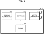
- FIG. 2 is a block diagram of the base station 110 according to embodiments.
- the base station 110 may include a wireless communicator 210, a backhaul communicator 220, a storage 230, and a controller 240.
- the wireless communicator 210 may perform functions for transmission and reception of signals through a wireless channel. According to an embodiment, the wireless communicator 210 may perform conversion between a baseband signal and a bitstream according to the physical layer standard of a system. For example, the wireless communicator 210 may generate complex symbols by encoding and modulating a transmitted bitstream during data transmission and reconstruct a received bitstream by demodulating and decoding a baseband signal during data reception. The wireless communicator 210 may up-convert a baseband signal into a radio frequency (RF) band signal and transmit the RF band signal through an antenna or may down-convert an RF band signal received through an antenna into a baseband signal.
- RF radio frequency
- the wireless communicator 210 may include a transmission filter, a reception filter, an amplifier, a mixer, an oscillator, a digital-to-analog converter (DAC), an analog-to-digital converter (ADC), and the like.
- DAC digital-to-analog converter
- ADC analog-to-digital converter
- the wireless communicator 210 may transmit and receive signals. For example, the wireless communicator 210 may transmit a synchronization signal, a reference signal, system information, a message, control information, data, or the like. The wireless communicator 210 may perform beamforming. To give an orientation to a signal to be transmitted or received, the wireless communicator 210 may apply a beamforming weight to the signal. The wireless communicator 210 may change a formed beam and repeatedly transmit a signal.
- the backhaul communicator 220 may provide an interface for communication with other nodes in a network.
- the backhaul communicator 220 may convert a bitstream, which is transmitted from the base station 110 to another node, e.g., another access node, another base station, an upper node, or a core network, into a physical signal and may convert a physical signal received from another node into a bitstream.
- another node e.g., another access node, another base station, an upper node, or a core network
- the storage 230 may store data, such as a basic program for the operation of the base station 110, an application program, configuration information, or the like.
- the storage 230 may include volatile memory, non-volatile memory, or a combination of volatile memory and non-volatile memory.
- the storage 230 may provide stored data at the request of the controller 240.
- the controller 240 may control operations of the base station 110.
- the controller 240 may transmit and receive signals through the wireless communicator 210 or the backhaul communicator 220.
- the controller 240 may write data to and read data from the storage 230.
- the controller 240 may include at least one processor.
- FIG. 3 is a block diagram of the electronic device 120 according to embodiments.
- the electronic device 120 may include a communicator 310, a storage 320, and a controller 330.
- the communicator 310 may perform functions for transmission and reception of signals through a wireless channel. For example, the communicator 310 may perform conversion between a baseband signal and a bitstream according to the physical layer standard of a system. For example, the communicator 310 may generate complex symbols by encoding and modulating a transmitted bitstream during data transmission and reconstruct a received bitstream by demodulating and decoding a baseband signal during data reception. The communicator 310 may up-convert a baseband signal into an RF band signal and transmit the RF band signal through an antenna or may down-convert an RF band signal received through an antenna into a baseband signal.
- the communicator 310 may include a transmission filter, a reception filter, an amplifier, a mixer, an oscillator, a DAC, an ADC, and the like.
- the communicator 310 may perform beamforming. To give an orientation to a signal to be transmitted or received, the communicator 310 may apply a beamforming weight to the signal.
- the communicator 310 may transmit and receive signals.
- the communicator 310 may receive a downlink signal.
- the downlink signal may include a synchronization signal, a reference signal, system information, a configuration message, control information, downlink data, or the like.
- the communicator 310 may transmit an uplink signal.
- the uplink signal may include a signal related to random access, a reference signal (e.g., a sounding reference signal (SRS) or demodulation reference signal (DM-RS)), or uplink data.
- a reference signal e.g., a sounding reference signal (SRS) or demodulation reference signal (DM-RS)
- the storage 320 may store data, such as a basic program for the operation of the electronic device 120, an application program, configuration information, or the like.
- the storage 320 may include volatile memory, non-volatile memory, or a combination of volatile memory and non-volatile memory.
- the storage 320 may provide stored data at the request of the controller 330.
- the controller 330 may generally control operations of the electronic device 120. For example, the controller 330 may transmit and receive signals through the communicator 310. The controller 330 may write data to and read data from the storage 320. For these operations, the controller 330 may include at least one processor or microprocessor or may be part of a processor. When the controller 330 is part of a processor, part of the communicator 310 and the controller 330 may be referred to as a communication processor.
- the controller 330 may further include an interference estimation circuit 331 and a precoding matrix calculation circuit 333.
- the interference estimation circuit 331 may detect an interference signal that is input to the electronic device 120.
- the interference signal may include both spatially correlated interference and frequency selective interference.
- the spatially correlated interference may refer to interference that occurs because of a signal mainly generated from the neighboring base station 130 or 140 or another neighboring wireless communication device (e.g., another terminal).
- the frequency selective interference may refer to interference that occurs because of distortion of an edge signal in a frequency band, which is caused by using an alternative filter (e.g., a function shaped analog baseband filter (SINC)) because of the design limit of an ideal frequency filter (e.g., a rectangular filter).
- SINC function shaped analog baseband filter
- the interference estimation circuit 331 may detect various interference signals including, for example, at least one of the spatially correlated interference and the frequency selective interference.
- the interference estimation circuit 331 may generate an interference covariance matrix corresponding to the detected interference signals and transmit the interference covariance matrix to the precoding matrix calculation circuit 333.
- the precoding matrix calculation circuit 333 may calculate a precoding matrix. According to an embodiment, the precoding matrix calculation circuit 333 may receive, from the interference estimation circuit 331, an interference covariance matrix corresponding to a result of detecting interference signals. The precoding matrix calculation circuit 333 may convert the interference covariance matrix into an SRS precoding matrix. The precoding matrix calculation circuit 333 may transmit the SRS precoding matrix to a precoder such that an SRS to be transmitted to the base station 110 may be multiplied by the SRS precoding matrix.
- FIG. 4A illustrates an example of a detailed configuration of the communicator 310 in FIG. 3 .
- FIG. 4A illustrates elements for performing hybrid beamforming when transmitting a radio signal.
- the communicator 310 may include an encoder and modulator 410, a digital beamformer 420, first to N-th transmission paths 430-1 to 430-N, and an analog beamformer 440.
- the encoder and modulator 410 may perform channel encoding. For channel encoding, at least one of a low density parity check (LDPC) code, a convolution code, and a polar code may be used.
- LDPC low density parity check
- the encoder and modulator 410 may generate modulated symbols by performing constellation mapping.
- the digital beamformer 420 may perform beamforming on digital signals (e.g., modulated symbols). For example, the digital beamformer 420 may multiply the modulated symbols by beamforming weights. In embodiments, the beamforming weights may be used to change the magnitude and phase of a signal and called a precoding matrix or a precoder. The digital beamformer 420 may output digitally beamformed modulated symbols respectively to the first to N-th transmission paths 430-1 to 430-N. In embodiments, according to a multiple-input multiple-output (MIMO) transmission scheme, the modulated symbols may be multiplexed, or the same modulated symbols may be provided to the first to N-th transmission paths 430-1 to 430-N.
- MIMO multiple-input multiple-output
- the first to N-th transmission paths 430-1 to 430-N may convert digitally beamformed digital signals into analog signals.
- each of the first to N-th transmission paths 430-1 to 430-N may include an inverse fast Fourier transform (IFFT) operator, a cyclic prefix (CP) inserter, a DAC, and an up-converter.
- the CP inserter may be used for an orthogonal frequency division multiplexing (OFDM) scheme, and may be omitted in embodiments in which a different physical layer scheme (e.g., a filter bank multi-carrier (FBMC) scheme) is used.
- OFDM orthogonal frequency division multiplexing
- FBMC filter bank multi-carrier
- the first to N-th transmission paths 430-1 to 430-N may provide independent signal processing for multiple streams generated through digital beamforming. However, in embodiments, some of the elements of the first to N-th transmission paths 430-1 to 430-N may be shared.
- the analog beamformer 440 may perform beamforming on analog signals. For example, the analog beamformer 440 may multiply the analog signals by beamforming weights. In embodiments, the beamforming weights may be used to change the magnitude and phase of a signal.
- FIG. 4B illustrates an example of a detailed configuration of the communicator 310 in FIG. 3 .
- FIG. 4B illustrates elements for performing hybrid beamforming when receiving a radio signal.
- the communicator 310 may include a decoder and demodulator 450, a digital beamformer 460, first to N-th reception paths 470-1 to 470-N, and an analog beamformer 480.
- the decoder and demodulator 450 may perform channel decoding.
- channel decoding at least one of an LDPC code, a convolution code, a polar code, and a turbo code may be used.
- the digital beamformer 460 and the analog beamformer 480 may respectively correspond to the digital beamformer 420 and the analog beamformer 440 in FIG. 4A .
- the first to N-th reception paths 470-1 to 470-N may convert beamformed analog signals into digital signals.
- each of the first to N-th reception paths 470-1 to 470-N may include a fast Fourier transform (FFT) operator, an ADC, a CP remover, a serial-to-parallel converter, and a down-converter.
- FFT fast Fourier transform
- each of the first to N-th reception paths 470-1 to 470-N may generate a serial time-domain baseband signal by down-converting a received signal into a baseband frequency and removing a CP from the received signal, convert the serial time-domain baseband signal into parallel time-domain signals, generate N parallel frequency-domain signals by performing an FFT algorithm on the parallel time-domain signals, and convert the N parallel frequency-domain signals into a sequence of modulated data symbols.
- the first to N-th reception paths 470-1 to 470-N may provide independent signal processing for multiple streams generated through analog beamforming. However, in embodiments, some of the elements of the first to N-th reception paths 470-1 to 470-N may be shared.
- FIG. 5 illustrates an antenna port according to embodiments.
- a base station 110 may communicate with an electronic device 120 by using MIMO.
- the base station 110 may include a plurality of antennas, e.g., first and second antennas Ant1_1 and Ant1_2, and the electronic device 120 may include a plurality of antennas, e.g., third and fourth antennas Ant2_1 and Ant2_2.
- each of the base station 110 and the electronic device 120 are illustrated in FIG. 5 as including two antennas (e.g., the first and second antennas Ant1_1 and Ant1_2 or the third and fourth antennas Ant2_1 and Ant2_2), embodiments are not limited thereto.
- each of the base station 110 and the electronic device 120 may include, for example, three or more antennas.
- the base station 110 may include a first transceiver 11, a second transceiver 12, the first antenna Ant1_1, and the second antenna Ant1_2. Each of the first transceiver 11 and the second transceiver 12 may be connected to a single antenna. For example, the first transceiver 11 may be connected to the first antenna Ant1_1, and the second transceiver 12 may be connected to the second antenna Ant1_2. When the base station 110 operates as a transmitting device, the first transceiver 11 and the second transceiver 12 may operate as transmitters. When the base station 110 operates as a receiving device, the first transceiver 11 and the second transceiver 12 may operate as receivers.
- the first transceiver 11 may generate a first signal Sig by merging a first component carrier C1 with a second component carrier C2, and output the first signal Sig to the electronic device 120.
- the first transceiver 11 may extract both the first component carrier C1 and the second component carrier C2 from the first signal Sig.
- each of the first transceiver 11 and the second transceiver 12 may not individually transmit a single component carrier, but may instead merge and transmit a plurality of component carriers.
- each of the first transceiver 11 and the second transceiver 12 may not extract only a single component carrier, but may instead extract a plurality of component carriers.
- the electronic device 120 may include a third transceiver 21, a fourth transceiver 22, the third antenna Ant2_1, and the fourth antenna Ant2_2.
- the electronic device 120 may be substantially the same as, or may be similar to, the base station 110, and thus, redundant descriptions thereof may be omitted.
- FIG. 6 is a flowchart of an operating method of the electronic device 120, according to embodiments.
- the electronic device 120 may obtain an interference covariance matrix by performing interference estimation in operation S110.
- the electronic device 120 may perform interference estimation using the interference estimation circuit 331 of the controller 330.
- An inter-cell signal may be a target of the interference estimation.
- the electronic device 120 may receive, as interference signals, signals transmitted from the neighboring base stations 130 and 140.
- the electronic device 120 may directly estimate an interference channel when the pattern of an interference signal is known. For example, when the electronic device 120 has established a radio resource control (RRC) connection with the neighboring base stations 130 and 140, the electronic device 120 may store information about the transmission pattern of reference signals of the neighboring base stations 130 and 140. In embodiments, the electronic device 120 may receive, from the base station 110, and store information about the transmission pattern of reference signals of the neighboring base stations 130 and 140. In this case, the electronic device 120 may directly estimate an interference channel, based on the transmission pattern of interference signals of the neighboring base stations 130 and 140.
- RRC radio resource control
- the electronic device 120 may perform interference estimation without knowing the pattern of interference signals. For example, when the electronic device 120 has not established an RRC connection with the neighboring base stations 130 and 140 or has not received, from the base station 110, information about the transmission pattern of reference signals of the neighboring base stations 130 and 140, the electronic device 120 may indirectly estimate an interference channel. For example, the electronic device 120 may obtain an interference covariance matrix by subtracting a term of a reference signal, which has been agreed to be exchanged with the base station 110, from received signals and averaging results of the subtraction.
- the electronic device 120 may calculate an SRS precoding matrix based on the interference covariance matrix in operation S120.
- the SRS precoding matrix may be multiplied by an SRS that the electronic device 120 transmits to the base station 110.
- K NI may represent the interference covariance matrix
- W SRS may represent the SRS precoding matrix
- y DL may represent a downlink reception signal
- H DL may represent a downlink channel matrix
- W DL may represent a downlink precoding matrix
- x DL may represent a downlink transmission signal
- H I may represent an interference channel matrix with respect to L interference signal streams
- X I may represent an interference signal
- n DL may represent a noise signal.
- a downlink channel capacity may be given by Equation 3.
- C DL log 2 det I N + K D K NI ⁇ 1 .
- C DL may represent the downlink channel capacity
- Equation 5 may be used to determine K D and K NI .
- I N may represent identity matrix.
- E may represent an operator for mean calculation
- superscript H may represent an operator for conjugate transpose (Hermitian transpose)
- K D may represent a covariance matrix with respect to the downlink transmission signal
- K NI may represent a covariance matrix with respect to interference and noise signals
- ⁇ 2 I N may represent AWGN(Additive White Gaussian Noise) power.
- Equation 6 K NI ⁇ 1 2
- H DL USV
- H W DL optimal P 1 2 V
- U, S, and V may be calculated by singular value decomposition of an effective channel matrix H DL , which may be whitened considering interference information.
- P may represent a diagonal matrix in which each diagonal element indicates electrical power assigned to a stream. Electrical power may be determined by a water-filing algorithm, by which a channel gain of a stream is calculated based on a diagonal element of S.
- an environment with no interference signal may be considered, and an SRS that the electronic device 120 transmits to the base station 110 may be determined according to Equation 8.
- y SRS H UL x SRS + n UL
- y SRS may represent an uplink signal received by the base station 110
- H UL may represent an uplink channel matrix transmitted by the electronic device 120
- x SRS may represent an uplink transmission signal transmitted by the electronic device 120
- n UL may represent a noise signal.
- the base station 110 may estimate a downlink channel toward the electronic device 120 using Equation 9.
- H DL H UL T
- the base station 110 may obtain a downlink precoding matrix by transposing an uplink channel matrix, based on the channel reciprocity.
- Equation 10 may be determined.
- y SRS H UL K NI ⁇ 1 / 2 x SRS + n UL
- a precoding matrix optimizing a downlink channel capacity may be determined according to Equation 11.
- a downlink precoding matrix calculated by the base station 110 may be identical to a precoding matrix optimizing a downlink channel capacity.
- the electronic device 120 may transmit an SRS to the base station 110, based on the SRS precoding matrix, in operation S130.
- the precoding matrix calculation circuit 333 may provide the SRS precoding matrix to a precoder.
- the precoder may generate a transmission signal by multiplying an SRS to be transmitted to the base station 110 by the SRS precoding matrix.
- FIG. 7 illustrates signal exchanges between a base station and an electronic device, according to embodiments.
- the electronic device 120 may perform interference estimation in operation S210.
- the electronic device 120 may perform the interference estimation using the interference estimation circuit 331.
- An inter-cell signal may be a target of the interference estimation.
- the electronic device 120 may obtain an interference covariance matrix by subtracting a term of a reference signal, which has been agreed to be exchanged with the base station 110, from received signals, and averaging results of the subtraction.
- the electronic device 120 may calculate a precoding matrix in operation S220.
- the precoding matrix may include the SRS precoding matrix in FIG. 6 .
- the electronic device 120 may calculate the SRS precoding matrix based on an interference covariance matrix.
- the interference covariance matrix may be obtained based on a result of the interference estimation in operation S210.
- the electronic device 120 may transmit an SRS to the base station 110 in operation S230.
- the electronic device 120 may generate the SRS by multiplying, using a precoder, the SRS precoding matrix by a signal to be transmitted to the base station 110.
- the SRS may include a reference signal that has been precoded reflecting interference information of the electronic device 120.
- the base station 110 may estimate a downlink channel in operation S240.
- the base station 110 may estimate the downlink channel based on the SRS received from the electronic device 120. For example, the base station 110 may not recognize whether the SRS is multiplied with an SRS precoding matrix reflecting the interference information of the electronic device 120.
- the downlink channel estimated by the base station 110 may be a channel on which interference signals experienced by the electronic device 120 is considered.
- the base station 110 may calculate a downlink precoding matrix for a downlink signal, based on the downlink channel, in operation S250.
- the downlink precoding matrix may be a matrix that maximizes a downlink channel capacity.
- the base station 110 may transmit a physical downlink shared channel (PDSCH) signal to the electronic device 120 in operation S260.
- PDSCH physical downlink shared channel
- the PDSCH signal may be generated by multiplying a transmission signal by the downlink precoding matrix calculated in operation S250.
- FIG. 8 is a graph showing an increase of downlink channel capacity when interference is considered, according to an embodiment.
- the electronic device 120 and the base station 110 may be based on 4 ⁇ 4 MIMO.
- the electronic device 120 may transmit and receive signals using four different antenna ports, and the base station 110 may also transmit and receive signals using four different antenna ports.
- the electronic device 120 may not receive an interference signal from the neighboring base stations 130 and 140.
- the number of interferers may be 1.
- the downlink channel capacity increases when the electronic device 120 generates an SRS precoding matrix by performing interference estimation and transmits an SRS based on the SRS precoding matrix. Even when there are no interference signals from the neighboring base stations 130 and 140, there may still be a self-interference signal of the electronic device 120 or an interference signal from another neighboring electronic device. Thus, the downlink channel capacity may be increased even though the number of interferers corresponds to 1.
- the downlink channel capacity may decrease. For example, when there are two interferers, the electronic device 120 may receive an interference signal from the neighboring base station 130. When there are four interferers, the electronic device 120 may receive interference signals from three neighboring base stations. As the number of neighboring base stations transmitting an interference signal increases, the strength of the interference signal increases. Accordingly, a channel state may degrade, and channel capacity may decrease. However, in the cases of two interferers and four interferers, the downlink channel capacity may increase when an SRS is transmitted based on an SRS precoding matrix, according to embodiments.
- FIG. 9 is a block diagram of a wireless communication device according to an embodiment.
- a wireless communication device 1000 may include a modem and a radio frequency integrated circuit (RFIC) 1060.
- the modem may include an application specific integrated circuit (ASIC) 1010, an application specific instruction set processor (ASIP) 1030, a memory 1050, a main processor 1070, and a main memory 1090.
- ASIC application specific integrated circuit
- ASIP application specific instruction set processor
- the wireless communication device 1000 of FIG. 9 may correspond to the electronic device 120, according to an embodiment.
- the RFIC 1060 may be connected to an antenna Ant and may receive a signal from or transmit a signal to the outside using a wireless communication network.
- the ASIP 1030 may be customized for a specific purpose and may support an instruction set dedicated to a specific application and execute an instruction included in the instruction set.
- the memory 1050 may communicate with the ASIP 1030 and may store a plurality of instructions, which are executed by the ASIP 1030, as a non-transitory storage device.
- the memory 1050 may include any type of memory, such as random access memory (RAM), read-only memory (ROM), tape, a magnetic disk, an optical disk, volatile memory, non-volatile memory, or a combination thereof, which is accessible by the ASIP 1030.
- the main processor 1070 may control the wireless communication device 1000 by executing instructions.
- the main processor 1070 may control the ASIC 1010 and the ASIP 1030 and process data received through a wireless communication network or a user input to the wireless communication device 1000.
- the main processor 1070 may perform interference estimation based on a signal received by the wireless communication device 1000, calculate an SRS precoding matrix based on a covariance matrix with respect to interference and noise signals, and generate and transmit an SRS based on the SRS precoding matrix such that interference experienced by the wireless communication device 1000 may be considered. Accordingly, a downlink channel capacity or a downlink data rate may be increased.
- the main memory 1090 may communicate with the main processor 1070 and may store a plurality of instructions, which are executed by the main processor 1070, as a non-transitory storage device.
- the main memory 1090 may include any type of memory, such as RAM, ROM, tape, a magnetic disk, an optical disk, volatile memory, non-volatile memory, or a combination thereof, which is accessible by the main processor 1070.
Landscapes
- Engineering & Computer Science (AREA)
- Signal Processing (AREA)
- Computer Networks & Wireless Communication (AREA)
- Power Engineering (AREA)
- Mobile Radio Communication Systems (AREA)
- Noise Elimination (AREA)
Abstract
Description
- The disclosure relates to a method of transmitting a signal and an electronic device, and more particularly, to an electronic device for transmitting a sounding reference signal (SRS) in a wireless communication system and an operating method thereof.
- To meet wireless data traffic demand that is growing since commercialization of 4th generation (4G) communication systems, many efforts have been put to develop improved 5th generation (5G) or pre-5G communication systems. For this reason, 5G or pre-5G communication systems are also called new radio (NR) systems in the 3rd Generation Partnership Project (3GPP) standard.
- To achieve a high data transmission rate, 5G communication systems are considered to be embodied in a millimeter wave (mmWave) band (e.g., a 28-GHz band or a 39-GHz band). To alleviate the path loss of radio waves and increase the propagation range of radio waves in the mmWave band, beamforming, massive multiple-input multiple-output (MIMO), full dimension MIMO (FD-MIMO), array antenna, analog beamforming, hybrid beamforming, and large scale antenna techniques are being examined.
- Provided are an electronic device for generating a precoding matrix by using an interference estimation result of a terminal and transmitting a sounding reference signal (SRS), based on the precoding matrix, and an operating method thereof.
- Additional aspects will be set forth in part in the description which follows and, in part, will be apparent from the description, or may be learned by practice of the presented embodiments.
- In accordance with an aspect of the disclosure, an electronic device includes a communication circuit configured to receive a reception signal including an interference signal, and to transmit a sounding reference signal (SRS) to a base station; and a control circuit comprising an interference estimation circuit configured to detect the interference signal in the reception signal, and a precoding matrix calculation circuit configured to generate an SRS precoding matrix corresponding to the SRS, based on a detection result obtained by the interference estimation circuit, wherein the control circuit is configured to control the communication circuit to transmit the SRS to the base station, and wherein the SRS is generated by multiplying a transmission signal by the SRS precoding matrix.
- In accordance with an aspect of the disclosure, an operating method of an electronic device includes performing interference estimation based on a reception signal including an interference signal; generating a sounding reference signal (SRS) precoding matrix, based on a result of the interference estimation; and transmitting an SRS to a base station, wherein the SRS is generated by multiplying a transmission signal by the SRS precoding matrix.
- In accordance with an aspect of the disclosure, a wireless communication system includes a base station configured to estimate a downlink channel based on a sounding reference signal (SRS); and an electronic device including: a communication circuit configured to perform at least one from among transmitting the SRS to the base station and receiving a reception signal including an interference signal, and a control circuit comprising an interference estimation circuit configured to detect the interference signal in the reception signal, and a precoding matrix calculation circuit configured to generate an SRS precoding matrix corresponding to the SRS, based on a detection result obtained by the interference estimation circuit, wherein the control circuit is configured to control the communication circuit to transmit the SRS to the base station, and wherein the SRS is generated by multiplying a transmission signal by the SRS precoding matrix.
- In accordance with an aspect of the disclosure, an electronic device includes a communication circuit configured to communicate with a base station; and a control circuit configured to: control the communication circuit to obtain a reception signal from the base station, detect an interference signal in the reception signal, generate a sounding reference signal (SRS) precoding matrix based on the interference signal, generate a SRS by multiplying a transmission signal by the SRS precoding matrix, and control the communication circuit to transmit the SRS to the base station.
- At least some of the above and other features of the invention are set out in the claims.
- The above and other aspects, features, and advantages of certain embodiments of the present disclosure will be more apparent from the following description taken in conjunction with the accompanying drawings in which:
-
FIG. 1 illustrates a wireless communication system according to an embodiment; -
FIG. 2 is a block diagram of a base station according to embodiments; -
FIG. 3 is a block diagram of an electronic device according to embodiments; -
FIG. 4A illustrates an example of the detailed configuration of a communicator inFIG. 3 , according to embodiments; -
FIG. 4B illustrates an example of the detailed configuration of a communicator inFIG. 3 , according to embodiments; -
FIG. 5 illustrates an antenna port according to embodiments; -
FIG. 6 is a flowchart of an operating method of an electronic device, according to embodiments; -
FIG. 7 illustrates signal exchanges between a base station and an electronic device, according to embodiments; -
FIG. 8 is a graph showing the increase of downlink channel capacity, according to embodiments; and -
FIG. 9 is a block diagram of a wireless communication device according to embodiments. - Hereinafter, embodiments are described in detail with reference to the accompanying drawings.
- As is traditional in the field, embodiments may be described and illustrated in terms of blocks which carry out a described function or functions. These blocks, as shown in the drawings, which may be referred to herein as "units" or "modules" or the like, may be physically implemented by analog or digital circuits such as logic gates, integrated circuits, microprocessors, microcontrollers, memory circuits, passive electronic components, active electronic components, optical components, hardwired circuits, or the like, and may be driven by firmware and software. The circuits may, for example, be embodied in one or more semiconductor chips, or on substrate supports such as printed circuit boards and the like. Circuits included in a block may be implemented by dedicated hardware, or by a processor (e.g., one or more programmed microprocessors and associated circuitry), or by a combination of dedicated hardware to perform some functions of the block and a processor to perform other functions of the block. Each block of the embodiments may be physically separated into two or more interacting and discrete blocks. Likewise, the blocks of the embodiments may be physically combined into more complex blocks.
-
FIG. 1 illustrates a wireless communication system according to an embodiment. - Referring to
FIG. 1 , a wireless communication system may include abase station 110, anelectronic device 120, and neighboringbase stations - According to various embodiments, the
base station 110 may be a network infrastructure that provides wireless access to theelectronic device 120. Thebase station 110 may have coverage that is determined by a certain geometrical area based on a distance, by which a signal may be transmitted. Thebase station 110 may be referred to as an access point (AP), an evolved-node B (eNodeB or eNB), a 5th generation (5G) node, a wireless point, or another term having a technical meaning equivalent thereto. - According to various embodiments, the
base station 110 may be connected to at least one transmission/reception point (TRP). Thebase station 110 may transmit a downlink signal to theelectronic device 120 or receive an uplink signal from theelectronic device 120 through at least one TRP. - According to various embodiments, as a device used by a user, the
electronic device 120 may communicate with thebase station 110 through a wireless channel. Theelectronic device 120 may be referred to as a terminal, a user equipment (UE), a mobile station, a subscriber station, a customer premises equipment (CPE), a remote terminal, a wireless terminal, a user device, or another term having a technical meaning equivalent thereto. - According to various embodiments, the
electronic device 120 may receive interference signals from the neighboringbase stations electronic device 120 may receive a downlink signal from thebase station 110, and simultaneously signals generated by the neighboringbase stations -
FIG. 2 is a block diagram of thebase station 110 according to embodiments. - Referring to
FIG. 2 , thebase station 110 may include awireless communicator 210, abackhaul communicator 220, astorage 230, and acontroller 240. - The
wireless communicator 210 may perform functions for transmission and reception of signals through a wireless channel. According to an embodiment, thewireless communicator 210 may perform conversion between a baseband signal and a bitstream according to the physical layer standard of a system. For example, thewireless communicator 210 may generate complex symbols by encoding and modulating a transmitted bitstream during data transmission and reconstruct a received bitstream by demodulating and decoding a baseband signal during data reception. Thewireless communicator 210 may up-convert a baseband signal into a radio frequency (RF) band signal and transmit the RF band signal through an antenna or may down-convert an RF band signal received through an antenna into a baseband signal. For these operations, thewireless communicator 210 may include a transmission filter, a reception filter, an amplifier, a mixer, an oscillator, a digital-to-analog converter (DAC), an analog-to-digital converter (ADC), and the like. - The
wireless communicator 210 may transmit and receive signals. For example, thewireless communicator 210 may transmit a synchronization signal, a reference signal, system information, a message, control information, data, or the like. Thewireless communicator 210 may perform beamforming. To give an orientation to a signal to be transmitted or received, thewireless communicator 210 may apply a beamforming weight to the signal. Thewireless communicator 210 may change a formed beam and repeatedly transmit a signal. - The
backhaul communicator 220 may provide an interface for communication with other nodes in a network. For example, thebackhaul communicator 220 may convert a bitstream, which is transmitted from thebase station 110 to another node, e.g., another access node, another base station, an upper node, or a core network, into a physical signal and may convert a physical signal received from another node into a bitstream. - The
storage 230 may store data, such as a basic program for the operation of thebase station 110, an application program, configuration information, or the like. Thestorage 230 may include volatile memory, non-volatile memory, or a combination of volatile memory and non-volatile memory. Thestorage 230 may provide stored data at the request of thecontroller 240. - The
controller 240 may control operations of thebase station 110. For example, thecontroller 240 may transmit and receive signals through thewireless communicator 210 or thebackhaul communicator 220. Thecontroller 240 may write data to and read data from thestorage 230. For these operations, thecontroller 240 may include at least one processor. -
FIG. 3 is a block diagram of theelectronic device 120 according to embodiments. - Referring to
FIG. 3 , theelectronic device 120 may include acommunicator 310, astorage 320, and acontroller 330. - The
communicator 310 may perform functions for transmission and reception of signals through a wireless channel. For example, thecommunicator 310 may perform conversion between a baseband signal and a bitstream according to the physical layer standard of a system. For example, thecommunicator 310 may generate complex symbols by encoding and modulating a transmitted bitstream during data transmission and reconstruct a received bitstream by demodulating and decoding a baseband signal during data reception. Thecommunicator 310 may up-convert a baseband signal into an RF band signal and transmit the RF band signal through an antenna or may down-convert an RF band signal received through an antenna into a baseband signal. For example, thecommunicator 310 may include a transmission filter, a reception filter, an amplifier, a mixer, an oscillator, a DAC, an ADC, and the like. Thecommunicator 310 may perform beamforming. To give an orientation to a signal to be transmitted or received, thecommunicator 310 may apply a beamforming weight to the signal. - The
communicator 310 may transmit and receive signals. Thecommunicator 310 may receive a downlink signal. The downlink signal may include a synchronization signal, a reference signal, system information, a configuration message, control information, downlink data, or the like. Thecommunicator 310 may transmit an uplink signal. The uplink signal may include a signal related to random access, a reference signal (e.g., a sounding reference signal (SRS) or demodulation reference signal (DM-RS)), or uplink data. - The
storage 320 may store data, such as a basic program for the operation of theelectronic device 120, an application program, configuration information, or the like. Thestorage 320 may include volatile memory, non-volatile memory, or a combination of volatile memory and non-volatile memory. Thestorage 320 may provide stored data at the request of thecontroller 330. - The
controller 330 may generally control operations of theelectronic device 120. For example, thecontroller 330 may transmit and receive signals through thecommunicator 310. Thecontroller 330 may write data to and read data from thestorage 320. For these operations, thecontroller 330 may include at least one processor or microprocessor or may be part of a processor. When thecontroller 330 is part of a processor, part of thecommunicator 310 and thecontroller 330 may be referred to as a communication processor. - According to an embodiment, the
controller 330 may further include aninterference estimation circuit 331 and a precodingmatrix calculation circuit 333. Theinterference estimation circuit 331 may detect an interference signal that is input to theelectronic device 120. For example, the interference signal may include both spatially correlated interference and frequency selective interference. The spatially correlated interference may refer to interference that occurs because of a signal mainly generated from the neighboringbase station interference estimation circuit 331 may detect various interference signals including, for example, at least one of the spatially correlated interference and the frequency selective interference. Theinterference estimation circuit 331 may generate an interference covariance matrix corresponding to the detected interference signals and transmit the interference covariance matrix to the precodingmatrix calculation circuit 333. - The precoding
matrix calculation circuit 333 may calculate a precoding matrix. According to an embodiment, the precodingmatrix calculation circuit 333 may receive, from theinterference estimation circuit 331, an interference covariance matrix corresponding to a result of detecting interference signals. The precodingmatrix calculation circuit 333 may convert the interference covariance matrix into an SRS precoding matrix. The precodingmatrix calculation circuit 333 may transmit the SRS precoding matrix to a precoder such that an SRS to be transmitted to thebase station 110 may be multiplied by the SRS precoding matrix. -
FIG. 4A illustrates an example of a detailed configuration of thecommunicator 310 inFIG. 3 . In detail,FIG. 4A illustrates elements for performing hybrid beamforming when transmitting a radio signal. - Referring to
FIG. 4A , thecommunicator 310 may include an encoder andmodulator 410, adigital beamformer 420, first to N-th transmission paths 430-1 to 430-N, and ananalog beamformer 440. - The encoder and
modulator 410 may perform channel encoding. For channel encoding, at least one of a low density parity check (LDPC) code, a convolution code, and a polar code may be used. The encoder andmodulator 410 may generate modulated symbols by performing constellation mapping. - The
digital beamformer 420 may perform beamforming on digital signals (e.g., modulated symbols). For example, thedigital beamformer 420 may multiply the modulated symbols by beamforming weights. In embodiments, the beamforming weights may be used to change the magnitude and phase of a signal and called a precoding matrix or a precoder. Thedigital beamformer 420 may output digitally beamformed modulated symbols respectively to the first to N-th transmission paths 430-1 to 430-N. In embodiments, according to a multiple-input multiple-output (MIMO) transmission scheme, the modulated symbols may be multiplexed, or the same modulated symbols may be provided to the first to N-th transmission paths 430-1 to 430-N. - The first to N-th transmission paths 430-1 to 430-N may convert digitally beamformed digital signals into analog signals. For example, each of the first to N-th transmission paths 430-1 to 430-N may include an inverse fast Fourier transform (IFFT) operator, a cyclic prefix (CP) inserter, a DAC, and an up-converter. The CP inserter may be used for an orthogonal frequency division multiplexing (OFDM) scheme, and may be omitted in embodiments in which a different physical layer scheme (e.g., a filter bank multi-carrier (FBMC) scheme) is used. For example, the first to N-th transmission paths 430-1 to 430-N may provide independent signal processing for multiple streams generated through digital beamforming. However, in embodiments, some of the elements of the first to N-th transmission paths 430-1 to 430-N may be shared.
- The
analog beamformer 440 may perform beamforming on analog signals. For example, theanalog beamformer 440 may multiply the analog signals by beamforming weights. In embodiments, the beamforming weights may be used to change the magnitude and phase of a signal. -
FIG. 4B illustrates an example of a detailed configuration of thecommunicator 310 inFIG. 3 . In detail,FIG. 4B illustrates elements for performing hybrid beamforming when receiving a radio signal. - According to various embodiments, the
communicator 310 may include a decoder anddemodulator 450, adigital beamformer 460, first to N-th reception paths 470-1 to 470-N, and ananalog beamformer 480. - The decoder and
demodulator 450 may perform channel decoding. For the channel decoding, at least one of an LDPC code, a convolution code, a polar code, and a turbo code may be used. - According to various embodiments, the
digital beamformer 460 and theanalog beamformer 480 may respectively correspond to thedigital beamformer 420 and theanalog beamformer 440 inFIG. 4A . - The first to N-th reception paths 470-1 to 470-N may convert beamformed analog signals into digital signals. For example, each of the first to N-th reception paths 470-1 to 470-N may include a fast Fourier transform (FFT) operator, an ADC, a CP remover, a serial-to-parallel converter, and a down-converter. In detail, each of the first to N-th reception paths 470-1 to 470-N may generate a serial time-domain baseband signal by down-converting a received signal into a baseband frequency and removing a CP from the received signal, convert the serial time-domain baseband signal into parallel time-domain signals, generate N parallel frequency-domain signals by performing an FFT algorithm on the parallel time-domain signals, and convert the N parallel frequency-domain signals into a sequence of modulated data symbols. For example, the first to N-th reception paths 470-1 to 470-N may provide independent signal processing for multiple streams generated through analog beamforming. However, in embodiments, some of the elements of the first to N-th reception paths 470-1 to 470-N may be shared.
-
FIG. 5 illustrates an antenna port according to embodiments. - Referring to
FIG. 5 , abase station 110 may communicate with anelectronic device 120 by using MIMO. For the communication, thebase station 110 may include a plurality of antennas, e.g., first and second antennas Ant1_1 and Ant1_2, and theelectronic device 120 may include a plurality of antennas, e.g., third and fourth antennas Ant2_1 and Ant2_2. Although each of thebase station 110 and theelectronic device 120 are illustrated inFIG. 5 as including two antennas (e.g., the first and second antennas Ant1_1 and Ant1_2 or the third and fourth antennas Ant2_1 and Ant2_2), embodiments are not limited thereto. In embodiments, each of thebase station 110 and theelectronic device 120 may include, for example, three or more antennas. - The
base station 110 may include afirst transceiver 11, asecond transceiver 12, the first antenna Ant1_1, and the second antenna Ant1_2. Each of thefirst transceiver 11 and thesecond transceiver 12 may be connected to a single antenna. For example, thefirst transceiver 11 may be connected to the first antenna Ant1_1, and thesecond transceiver 12 may be connected to the second antenna Ant1_2. When thebase station 110 operates as a transmitting device, thefirst transceiver 11 and thesecond transceiver 12 may operate as transmitters. When thebase station 110 operates as a receiving device, thefirst transceiver 11 and thesecond transceiver 12 may operate as receivers. - In a transmission mode, the
first transceiver 11 may generate a first signal Sig by merging a first component carrier C1 with a second component carrier C2, and output the first signal Sig to theelectronic device 120. Thefirst transceiver 11 may extract both the first component carrier C1 and the second component carrier C2 from the first signal Sig. In embodiments, each of thefirst transceiver 11 and thesecond transceiver 12 may not individually transmit a single component carrier, but may instead merge and transmit a plurality of component carriers. In embodiments, each of thefirst transceiver 11 and thesecond transceiver 12 may not extract only a single component carrier, but may instead extract a plurality of component carriers. - The
electronic device 120 may include athird transceiver 21, afourth transceiver 22, the third antenna Ant2_1, and the fourth antenna Ant2_2. Theelectronic device 120 may be substantially the same as, or may be similar to, thebase station 110, and thus, redundant descriptions thereof may be omitted. -
FIG. 6 is a flowchart of an operating method of theelectronic device 120, according to embodiments. - Referring to
FIG. 6 , theelectronic device 120 may obtain an interference covariance matrix by performing interference estimation in operation S110. Theelectronic device 120 may perform interference estimation using theinterference estimation circuit 331 of thecontroller 330. An inter-cell signal may be a target of the interference estimation. For example, theelectronic device 120 may receive, as interference signals, signals transmitted from the neighboringbase stations - According to an embodiment, the
electronic device 120 may directly estimate an interference channel when the pattern of an interference signal is known. For example, when theelectronic device 120 has established a radio resource control (RRC) connection with the neighboringbase stations electronic device 120 may store information about the transmission pattern of reference signals of the neighboringbase stations electronic device 120 may receive, from thebase station 110, and store information about the transmission pattern of reference signals of the neighboringbase stations electronic device 120 may directly estimate an interference channel, based on the transmission pattern of interference signals of the neighboringbase stations - According to an embodiment, the
electronic device 120 may perform interference estimation without knowing the pattern of interference signals. For example, when theelectronic device 120 has not established an RRC connection with the neighboringbase stations base station 110, information about the transmission pattern of reference signals of the neighboringbase stations electronic device 120 may indirectly estimate an interference channel. For example, theelectronic device 120 may obtain an interference covariance matrix by subtracting a term of a reference signal, which has been agreed to be exchanged with thebase station 110, from received signals and averaging results of the subtraction. - The
electronic device 120 may calculate an SRS precoding matrix based on the interference covariance matrix in operation S120. The SRS precoding matrix may be multiplied by an SRS that theelectronic device 120 transmits to thebase station 110. Theelectronic device 120 may calculate the SRS precodingmatrix using Equation 1 below:
- In embodiments, KNI may represent the interference covariance matrix, and WSRS may represent the SRS precoding matrix. An example process for deriving the SRS precoding matrix is described below.
- Downlink signals between the
base station 110 and theelectronic device 120 may be given byEquation 2 below:
- Here, yDL may represent a downlink reception signal, HDL may represent a downlink channel matrix, WDL may represent a downlink precoding matrix, xDL may represent a downlink transmission signal, HI may represent an interference channel matrix with respect to L interference signal streams, XI may represent an interference signal, and nDL may represent a noise signal.
- In embodiments, a downlink channel capacity may be given by
Equation 3.
- Here, CDL may represent the downlink channel capacity, and
Equation 4 and -
Equation 5 below may be used to determine KD and KNI. And, IN may represent identity matrix.

- In embodiments, E may represent an operator for mean calculation, superscript H may represent an operator for conjugate transpose (Hermitian transpose), KD may represent a covariance matrix with respect to the downlink transmission signal, KNI may represent a covariance matrix with respect to interference and noise signals, and σ 2 IN may represent AWGN(Additive White Gaussian Noise) power.
- Optimal downlink precoding for maximizing the downlink channel capacity of
Equation 3 may be calculated usingEquation 6 andEquation 7 below:

- In embodiments, U, S, and V may be calculated by singular value decomposition of an effective channel matrix
HDL , which may be whitened considering interference information. P may represent a diagonal matrix in which each diagonal element indicates electrical power assigned to a stream. Electrical power may be determined by a water-filing algorithm, by which a channel gain of a stream is calculated based on a diagonal element of S. - According to an embodiment, an environment with no interference signal may be considered, and an SRS that the
electronic device 120 transmits to thebase station 110 may be determined according toEquation 8.
- In embodiments, ySRS may represent an uplink signal received by the
base station 110, HUL may represent an uplink channel matrix transmitted by theelectronic device 120, xSRS may represent an uplink transmission signal transmitted by theelectronic device 120, and nUL may represent a noise signal. - Based on an assumption that channel reciprocity is valid, the
base station 110 may estimate a downlink channel toward theelectronic device 120 usingEquation 9.
- For example, in an environment with no interference, the
base station 110 may obtain a downlink precoding matrix by transposing an uplink channel matrix, based on the channel reciprocity. - According to various embodiments, based on an assumption that the
electronic device 120 transmits an SRS according to an SRS precoding matrix,Equation 10 may be determined.
- Referring to
Equations Equation 11.
- For example, it may be seen that when the
electronic device 120 transmits an SRS to thebase station 110 based on an SRS precoding matrix, a downlink precoding matrix calculated by thebase station 110 may be identical to a precoding matrix optimizing a downlink channel capacity. - The
electronic device 120 may transmit an SRS to thebase station 110, based on the SRS precoding matrix, in operation S130. For example, the precodingmatrix calculation circuit 333 may provide the SRS precoding matrix to a precoder. The precoder may generate a transmission signal by multiplying an SRS to be transmitted to thebase station 110 by the SRS precoding matrix. -
FIG. 7 illustrates signal exchanges between a base station and an electronic device, according to embodiments. - Referring to
FIG. 7 , theelectronic device 120 may perform interference estimation in operation S210. Theelectronic device 120 may perform the interference estimation using theinterference estimation circuit 331. An inter-cell signal may be a target of the interference estimation. For example, theelectronic device 120 may obtain an interference covariance matrix by subtracting a term of a reference signal, which has been agreed to be exchanged with thebase station 110, from received signals, and averaging results of the subtraction. - The
electronic device 120 may calculate a precoding matrix in operation S220. The precoding matrix may include the SRS precoding matrix inFIG. 6 . For example, theelectronic device 120 may calculate the SRS precoding matrix based on an interference covariance matrix. The interference covariance matrix may be obtained based on a result of the interference estimation in operation S210. - The
electronic device 120 may transmit an SRS to thebase station 110 in operation S230. For example, theelectronic device 120 may generate the SRS by multiplying, using a precoder, the SRS precoding matrix by a signal to be transmitted to thebase station 110. The SRS may include a reference signal that has been precoded reflecting interference information of theelectronic device 120. - The
base station 110 may estimate a downlink channel in operation S240. In embodiments, thebase station 110 may estimate the downlink channel based on the SRS received from theelectronic device 120. For example, thebase station 110 may not recognize whether the SRS is multiplied with an SRS precoding matrix reflecting the interference information of theelectronic device 120. The downlink channel estimated by thebase station 110 may be a channel on which interference signals experienced by theelectronic device 120 is considered. - The
base station 110 may calculate a downlink precoding matrix for a downlink signal, based on the downlink channel, in operation S250. In embodiments, the downlink precoding matrix may be a matrix that maximizes a downlink channel capacity. - The
base station 110 may transmit a physical downlink shared channel (PDSCH) signal to theelectronic device 120 in operation S260. In embodiments, the PDSCH signal may be generated by multiplying a transmission signal by the downlink precoding matrix calculated in operation S250. -
FIG. 8 is a graph showing an increase of downlink channel capacity when interference is considered, according to an embodiment. - Referring to
FIG. 8 , theelectronic device 120 and thebase station 110 may be based on 4×4 MIMO. For example, theelectronic device 120 may transmit and receive signals using four different antenna ports, and thebase station 110 may also transmit and receive signals using four different antenna ports. - According to an embodiment, the
electronic device 120 may not receive an interference signal from the neighboringbase stations electronic device 120 generates an SRS precoding matrix by performing interference estimation and transmits an SRS based on the SRS precoding matrix. Even when there are no interference signals from the neighboringbase stations electronic device 120 or an interference signal from another neighboring electronic device. Thus, the downlink channel capacity may be increased even though the number of interferers corresponds to 1. - According to an embodiment, as the number of interferers increases, the downlink channel capacity may decrease. For example, when there are two interferers, the
electronic device 120 may receive an interference signal from the neighboringbase station 130. When there are four interferers, theelectronic device 120 may receive interference signals from three neighboring base stations. As the number of neighboring base stations transmitting an interference signal increases, the strength of the interference signal increases. Accordingly, a channel state may degrade, and channel capacity may decrease. However, in the cases of two interferers and four interferers, the downlink channel capacity may increase when an SRS is transmitted based on an SRS precoding matrix, according to embodiments. -
FIG. 9 is a block diagram of a wireless communication device according to an embodiment. - Referring to
FIG. 9 , awireless communication device 1000 may include a modem and a radio frequency integrated circuit (RFIC) 1060. The modem may include an application specific integrated circuit (ASIC) 1010, an application specific instruction set processor (ASIP) 1030, amemory 1050, amain processor 1070, and amain memory 1090. Thewireless communication device 1000 ofFIG. 9 may correspond to theelectronic device 120, according to an embodiment. - The
RFIC 1060 may be connected to an antenna Ant and may receive a signal from or transmit a signal to the outside using a wireless communication network. TheASIP 1030 may be customized for a specific purpose and may support an instruction set dedicated to a specific application and execute an instruction included in the instruction set. Thememory 1050 may communicate with theASIP 1030 and may store a plurality of instructions, which are executed by theASIP 1030, as a non-transitory storage device. As a non-limiting example, thememory 1050 may include any type of memory, such as random access memory (RAM), read-only memory (ROM), tape, a magnetic disk, an optical disk, volatile memory, non-volatile memory, or a combination thereof, which is accessible by theASIP 1030. - The
main processor 1070 may control thewireless communication device 1000 by executing instructions. For example, themain processor 1070 may control theASIC 1010 and theASIP 1030 and process data received through a wireless communication network or a user input to thewireless communication device 1000. For example, themain processor 1070 may perform interference estimation based on a signal received by thewireless communication device 1000, calculate an SRS precoding matrix based on a covariance matrix with respect to interference and noise signals, and generate and transmit an SRS based on the SRS precoding matrix such that interference experienced by thewireless communication device 1000 may be considered. Accordingly, a downlink channel capacity or a downlink data rate may be increased. - The
main memory 1090 may communicate with themain processor 1070 and may store a plurality of instructions, which are executed by themain processor 1070, as a non-transitory storage device. As a non-limiting example, themain memory 1090 may include any type of memory, such as RAM, ROM, tape, a magnetic disk, an optical disk, volatile memory, non-volatile memory, or a combination thereof, which is accessible by themain processor 1070. - While embodiments have been particularly shown and described, it will be understood that various changes in form and details may be made therein without departing from the scope of the following claims.
Claims (15)
- An electronic device comprising:a communication circuit configured to receive a reception signal including an interference signal, and to transmit a sounding reference signal (SRS) to a base station; anda control circuit comprising an interference estimation circuit configured to detect the interference signal in the reception signal, and a precoding matrix calculation circuit configured to generate an SRS precoding matrix corresponding to the SRS, based on a detection result obtained by the interference estimation circuit,wherein the control circuit is configured to control the communication circuit to transmit the SRS to the base station, andwherein the SRS is generated by multiplying a transmission signal by the SRS precoding matrix.
- The electronic device of claim 1, wherein the interference estimation circuit is further configured to calculate a covariance matrix corresponding to a noise signal and the interference signal in the reception signal.
- The electronic device of claim 2, wherein the precoding matrix calculation circuit is further configured to receive the covariance matrix from the interference estimation circuit and calculate the SRS precoding matrix according to a following equation:

where KNI represents the covariance matrix, and WSRS represents the SRS precoding matrix. - The electronic device of any preceding claim, wherein the control circuit is further configured to:obtain, from the base station, information about a transmission pattern of a downlink signal transmitted by at least one neighboring base station; andestimate an interference channel based on the information about the transmission pattern.
- The electronic device of claim 3 or 4, wherein the communication circuit is further configured to:
receive a downlink signal based on a precoding matrix according to a downlink channel estimated by the base station using the SRS. - The electronic device of claim 5, wherein the SRS precoding matrix comprises a matrix which maximizes a capacity of the downlink channel estimated by the base station.
- The electronic device of claim 4, 5 or 6, wherein the information about the transmission pattern is obtained from the base station, based on one of a radio resource control (RRC) protocol, a media access control element (MAC CE), and downlink control information (DCI).
- An operating method of an electronic device, the operating method comprising:performing interference estimation based on a reception signal including an interference signal;generating a sounding reference signal (SRS) precoding matrix, based on a result of the interference estimation; andtransmitting an SRS to a base station,wherein the SRS is generated by multiplying a transmission signal by the SRS precoding matrix.
- The operating method of claim 8, wherein the result of the interference estimation corresponds to a covariance matrix based on noise and the interference signal in the reception signal.
- The operating method of claim 9, wherein the SRS precoding matrix is calculated using a following equation:

where WSRS represents the SRS precoding matrix, and KNI represents the covariance matrix. - The operating method of claim 8, 9 or 10, further comprising:obtaining, from the base station, information about a transmission pattern of a downlink signal transmitted by at least one neighboring base station; andestimating an interference channel based on the information about the transmission pattern.
- The operating method of claim 10 or 11, further comprising receiving a downlink signal based on a precoding matrix according to a downlink channel estimated by the base station using the SRS,
wherein the SRS precoding matrix includes a matrix which maximizes a capacity of the downlink channel estimated by the base station. - The operating method of claim 11 or 12, wherein the information about the transmission pattern is obtained from the base station, based on one of a radio resource control (RRC) protocol, a media access control element (MAC CE), and downlink control information (DCI).
- A wireless communication system comprising:a base station configured to estimate a downlink channel based on a sounding reference signal (SRS); andan electronic device comprising:a communication circuit configured to perform at least one from among transmitting the SRS to the base station and receiving a reception signal including an interference signal, anda control circuit comprising an interference estimation circuit configured to detect the interference signal in the reception signal, and a precoding matrix calculation circuit configured to generate an SRS precoding matrix corresponding to the SRS, based on a detection result obtained by the interference estimation circuit,wherein the control circuit is configured to control the communication circuit to transmit the SRS to the base station, andwherein the SRS is generated by multiplying a transmission signal by the SRS precoding matrix.
- The wireless communication system of claim 14, wherein the interference estimation circuit is further configured to calculate a covariance matrix corresponding to a noise signal and the interference signal in the reception signal.
Applications Claiming Priority (2)
| Application Number | Priority Date | Filing Date | Title |
|---|---|---|---|
| KR20220007451 | 2022-01-18 | ||
| KR1020220077816A KR20230111565A (en) | 2022-01-18 | 2022-06-24 | A method for transmitting sounding reference signal in wireless communication system and electronic device thereof |
Publications (2)
| Publication Number | Publication Date |
|---|---|
| EP4213402A2 true EP4213402A2 (en) | 2023-07-19 |
| EP4213402A3 EP4213402A3 (en) | 2023-08-16 |
Family
ID=84982510
Family Applications (1)
| Application Number | Title | Priority Date | Filing Date |
|---|---|---|---|
| EP23152285.5A Pending EP4213402A3 (en) | 2022-01-18 | 2023-01-18 | Electronic device for transmitting sounding reference signal in wireless communication system and operating method thereof |
Country Status (2)
| Country | Link |
|---|---|
| US (1) | US12500722B2 (en) |
| EP (1) | EP4213402A3 (en) |
Family Cites Families (13)
| Publication number | Priority date | Publication date | Assignee | Title |
|---|---|---|---|---|
| KR101639810B1 (en) | 2009-01-13 | 2016-07-25 | 엘지전자 주식회사 | Method of transmitting sounding reference signal in multiple antenna system |
| US9531514B2 (en) | 2009-12-03 | 2016-12-27 | Qualcomm Incorporated | Sounding reference signal enhancements for wireless communication |
| US9350475B2 (en) * | 2010-07-26 | 2016-05-24 | Qualcomm Incorporated | Physical layer signaling to user equipment in a wireless communication system |
| KR101719002B1 (en) | 2010-06-07 | 2017-03-23 | 엘지전자 주식회사 | Method and apparatus of transmitting aperiodic sounding reference signal in wireless communication system |
| CN104067667A (en) | 2012-01-23 | 2014-09-24 | 英特尔公司 | Network-assisted user association and offloading techniques for integrated multi-RAT heterogeneous networks |
| US9001780B2 (en) | 2012-01-27 | 2015-04-07 | Qualcomm Incorporated | Physical layer issues related to multi-TA group support |
| US9300451B2 (en) | 2013-03-13 | 2016-03-29 | Samsung Electronics Co., Ltd. | Transmission of sounding reference signals for adaptively configured TDD communication systems |
| US9813179B2 (en) | 2014-01-29 | 2017-11-07 | Mediatek Inc. | Method for cancelling a data transmission of a neighboring cell |
| KR102291457B1 (en) | 2014-09-03 | 2021-08-19 | 삼성전자주식회사 | Method and apparatus for estimating channel quality considering interference control and coordinated multi-point transmission and reception in cellular system |
| KR102306885B1 (en) | 2015-08-11 | 2021-09-30 | 삼성전자주식회사 | A method and apparatus for controlling a interference in a communication system using a plurality of anttenas |
| US10491279B2 (en) * | 2017-05-17 | 2019-11-26 | Qualcomm Incorporated | Precoded sounding reference signal transmission with asymmetric transmit and receive antennas |
| JP7351212B2 (en) | 2019-12-19 | 2023-09-27 | 日本電気株式会社 | Base stations and wireless communication systems |
| WO2023043578A1 (en) * | 2021-09-15 | 2023-03-23 | Qualcomm Incorporated | Techniques for control signal configuration for reference signal precoding |
-
2023
- 2023-01-17 US US18/097,944 patent/US12500722B2/en active Active
- 2023-01-18 EP EP23152285.5A patent/EP4213402A3/en active Pending
Also Published As
| Publication number | Publication date |
|---|---|
| EP4213402A3 (en) | 2023-08-16 |
| US20230231684A1 (en) | 2023-07-20 |
| US12500722B2 (en) | 2025-12-16 |
Similar Documents
| Publication | Publication Date | Title |
|---|---|---|
| JP6673824B2 (en) | Method and apparatus for transmitting a signal in a wireless communication system | |
| US7792226B2 (en) | Method and apparatus for carrier power and interference-noise estimation in space division multiple access and multiple-input/multiple-output wireless communication systems | |
| US8995543B2 (en) | Method and device for channel estimation with colliding interference cancellation | |
| KR102543091B1 (en) | Apparatus and method for integrated beamforming in wireless communication system | |
| US10135508B2 (en) | Method and apparatus for generating common signal in multiple input multiple output system | |
| US8867655B2 (en) | Apparatus and method for transmitting data using multiple antennas and beamforming | |
| EP4009551A1 (en) | Electronic device performing interference cancellation and operating method thereof | |
| US20130242896A1 (en) | Method and apparatus for receiving a signal in a wireless communication system that supports mu-mimo scheme | |
| US20140160968A1 (en) | Enhanced Use of Frequency Spectrum in a Wireless Communication Network | |
| US11356149B2 (en) | Apparatus and method for non-coherent joint detection in wireless communication systems | |
| EP4618439A1 (en) | Electronic device and method for processing received signal in wireless communication system | |
| US20250317329A1 (en) | Electronic device and method for receiving signal in wireless communication system | |
| EP3633873B1 (en) | Method for transmitting feedback information in wireless communication system and apparatus therefor | |
| EP4213402A2 (en) | Electronic device for transmitting sounding reference signal in wireless communication system and operating method thereof | |
| KR20240094949A (en) | Electronic device and method for processing received signal in wireless communication system | |
| US10917861B2 (en) | Radio device and radio cell with multiplexed data sequences with unequal power allocation | |
| CN116471000A (en) | Electronic device, operating method thereof, and wireless communication system | |
| US9277557B2 (en) | Radio base station and communication control method | |
| US20230300646A1 (en) | Method and device for preventing false pmi report in wireless communication system | |
| KR20230111565A (en) | A method for transmitting sounding reference signal in wireless communication system and electronic device thereof | |
| CN116405168B (en) | Cross-component carrier beam management method and device | |
| KR20230137217A (en) | Method and apparatus for preventing false pmi report in wireless communication system | |
| Hirakawa et al. | Development of Adaptive Array Antenna for Mobile WiMAX Uplink | |
| WO2024132377A1 (en) | Method and network node for transmission of wideband signals towards a wireless device through time domain beamforming | |
| Hirakawa et al. | Development of Interference Cancellation Method using Adaptive Array Antenna for Uplink OFDMA in Mobile WiMAX |
Legal Events
| Date | Code | Title | Description |
|---|---|---|---|
| PUAI | Public reference made under article 153(3) epc to a published international application that has entered the european phase |
Free format text: ORIGINAL CODE: 0009012 |
|
| STAA | Information on the status of an ep patent application or granted ep patent |
Free format text: STATUS: REQUEST FOR EXAMINATION WAS MADE |
|
| PUAL | Search report despatched |
Free format text: ORIGINAL CODE: 0009013 |
|
| 17P | Request for examination filed |
Effective date: 20230118 |
|
| AK | Designated contracting states |
Kind code of ref document: A2 Designated state(s): AL AT BE BG CH CY CZ DE DK EE ES FI FR GB GR HR HU IE IS IT LI LT LU LV MC ME MK MT NL NO PL PT RO RS SE SI SK SM TR |
|
| AK | Designated contracting states |
Kind code of ref document: A3 Designated state(s): AL AT BE BG CH CY CZ DE DK EE ES FI FR GB GR HR HU IE IS IT LI LT LU LV MC ME MK MT NL NO PL PT RO RS SE SI SK SM TR |
|
| RIC1 | Information provided on ipc code assigned before grant |
Ipc: H04B 7/0456 20170101AFI20230711BHEP |
|
| P01 | Opt-out of the competence of the unified patent court (upc) registered |
Effective date: 20231212 |
|
| STAA | Information on the status of an ep patent application or granted ep patent |
Free format text: STATUS: EXAMINATION IS IN PROGRESS |
|
| 17Q | First examination report despatched |
Effective date: 20250624 |