EP4212925A1 - Imaging element and imaging device - Google Patents
Imaging element and imaging device Download PDFInfo
- Publication number
- EP4212925A1 EP4212925A1 EP20957585.1A EP20957585A EP4212925A1 EP 4212925 A1 EP4212925 A1 EP 4212925A1 EP 20957585 A EP20957585 A EP 20957585A EP 4212925 A1 EP4212925 A1 EP 4212925A1
- Authority
- EP
- European Patent Office
- Prior art keywords
- photoelectric conversion
- imaging element
- groups
- structures
- group
- Prior art date
- Legal status (The legal status is an assumption and is not a legal conclusion. Google has not performed a legal analysis and makes no representation as to the accuracy of the status listed.)
- Pending
Links
- 238000003384 imaging method Methods 0.000 title claims abstract description 112
- 238000006243 chemical reaction Methods 0.000 claims abstract description 33
- 230000002093 peripheral effect Effects 0.000 claims description 29
- 238000012545 processing Methods 0.000 claims description 8
- 238000010586 diagram Methods 0.000 description 36
- 239000000463 material Substances 0.000 description 23
- 230000001629 suppression Effects 0.000 description 21
- 230000003287 optical effect Effects 0.000 description 17
- 238000000034 method Methods 0.000 description 14
- 238000013459 approach Methods 0.000 description 7
- GWEVSGVZZGPLCZ-UHFFFAOYSA-N Titan oxide Chemical compound O=[Ti]=O GWEVSGVZZGPLCZ-UHFFFAOYSA-N 0.000 description 6
- VYPSYNLAJGMNEJ-UHFFFAOYSA-N Silicium dioxide Chemical compound O=[Si]=O VYPSYNLAJGMNEJ-UHFFFAOYSA-N 0.000 description 4
- 239000003086 colorant Substances 0.000 description 4
- 239000011347 resin Substances 0.000 description 4
- 229920005989 resin Polymers 0.000 description 4
- 239000000758 substrate Substances 0.000 description 4
- 230000000694 effects Effects 0.000 description 3
- 239000011521 glass Substances 0.000 description 3
- 239000004065 semiconductor Substances 0.000 description 3
- 230000035945 sensitivity Effects 0.000 description 3
- 239000004642 Polyimide Substances 0.000 description 2
- UMIVXZPTRXBADB-UHFFFAOYSA-N benzocyclobutene Chemical compound C1=CC=C2CCC2=C1 UMIVXZPTRXBADB-UHFFFAOYSA-N 0.000 description 2
- 229910052681 coesite Inorganic materials 0.000 description 2
- 230000000052 comparative effect Effects 0.000 description 2
- 229910052906 cristobalite Inorganic materials 0.000 description 2
- 230000006866 deterioration Effects 0.000 description 2
- 239000004033 plastic Substances 0.000 description 2
- 229920003023 plastic Polymers 0.000 description 2
- 230000010287 polarization Effects 0.000 description 2
- 229920001721 polyimide Polymers 0.000 description 2
- 230000000644 propagated effect Effects 0.000 description 2
- 239000000377 silicon dioxide Substances 0.000 description 2
- 230000003595 spectral effect Effects 0.000 description 2
- 229910052682 stishovite Inorganic materials 0.000 description 2
- 229910052905 tridymite Inorganic materials 0.000 description 2
- 239000004925 Acrylic resin Substances 0.000 description 1
- 229920000178 Acrylic resin Polymers 0.000 description 1
- 229910002601 GaN Inorganic materials 0.000 description 1
- 229910001218 Gallium arsenide Inorganic materials 0.000 description 1
- 229910004541 SiN Inorganic materials 0.000 description 1
- 238000010521 absorption reaction Methods 0.000 description 1
- 239000011248 coating agent Substances 0.000 description 1
- 238000000576 coating method Methods 0.000 description 1
- 238000004891 communication Methods 0.000 description 1
- 230000010485 coping Effects 0.000 description 1
- 230000007423 decrease Effects 0.000 description 1
- 238000013461 design Methods 0.000 description 1
- 239000003822 epoxy resin Substances 0.000 description 1
- 238000003475 lamination Methods 0.000 description 1
- 238000012986 modification Methods 0.000 description 1
- 230000004048 modification Effects 0.000 description 1
- 229910003465 moissanite Inorganic materials 0.000 description 1
- 239000011368 organic material Substances 0.000 description 1
- 229920003229 poly(methyl methacrylate) Polymers 0.000 description 1
- 229920000647 polyepoxide Polymers 0.000 description 1
- 229920000642 polymer Polymers 0.000 description 1
- 239000004926 polymethyl methacrylate Substances 0.000 description 1
- 230000001902 propagating effect Effects 0.000 description 1
- 229910010271 silicon carbide Inorganic materials 0.000 description 1
- 238000004611 spectroscopical analysis Methods 0.000 description 1
- 239000011800 void material Substances 0.000 description 1
Images


Classifications
-
- H—ELECTRICITY
- H01—ELECTRIC ELEMENTS
- H01L—SEMICONDUCTOR DEVICES NOT COVERED BY CLASS H10
- H01L27/00—Devices consisting of a plurality of semiconductor or other solid-state components formed in or on a common substrate
- H01L27/14—Devices consisting of a plurality of semiconductor or other solid-state components formed in or on a common substrate including semiconductor components sensitive to infrared radiation, light, electromagnetic radiation of shorter wavelength or corpuscular radiation and specially adapted either for the conversion of the energy of such radiation into electrical energy or for the control of electrical energy by such radiation
- H01L27/144—Devices controlled by radiation
- H01L27/146—Imager structures
- H01L27/14601—Structural or functional details thereof
- H01L27/14625—Optical elements or arrangements associated with the device
- H01L27/14627—Microlenses
-
- H—ELECTRICITY
- H01—ELECTRIC ELEMENTS
- H01L—SEMICONDUCTOR DEVICES NOT COVERED BY CLASS H10
- H01L27/00—Devices consisting of a plurality of semiconductor or other solid-state components formed in or on a common substrate
- H01L27/14—Devices consisting of a plurality of semiconductor or other solid-state components formed in or on a common substrate including semiconductor components sensitive to infrared radiation, light, electromagnetic radiation of shorter wavelength or corpuscular radiation and specially adapted either for the conversion of the energy of such radiation into electrical energy or for the control of electrical energy by such radiation
- H01L27/144—Devices controlled by radiation
- H01L27/146—Imager structures
- H01L27/14601—Structural or functional details thereof
- H01L27/14625—Optical elements or arrangements associated with the device
-
- H—ELECTRICITY
- H01—ELECTRIC ELEMENTS
- H01L—SEMICONDUCTOR DEVICES NOT COVERED BY CLASS H10
- H01L27/00—Devices consisting of a plurality of semiconductor or other solid-state components formed in or on a common substrate
- H01L27/14—Devices consisting of a plurality of semiconductor or other solid-state components formed in or on a common substrate including semiconductor components sensitive to infrared radiation, light, electromagnetic radiation of shorter wavelength or corpuscular radiation and specially adapted either for the conversion of the energy of such radiation into electrical energy or for the control of electrical energy by such radiation
- H01L27/144—Devices controlled by radiation
- H01L27/146—Imager structures
- H01L27/14601—Structural or functional details thereof
- H01L27/14603—Special geometry or disposition of pixel-elements, address-lines or gate-electrodes
- H01L27/14605—Structural or functional details relating to the position of the pixel elements, e.g. smaller pixel elements in the center of the imager compared to pixel elements at the periphery
-
- H—ELECTRICITY
- H01—ELECTRIC ELEMENTS
- H01L—SEMICONDUCTOR DEVICES NOT COVERED BY CLASS H10
- H01L27/00—Devices consisting of a plurality of semiconductor or other solid-state components formed in or on a common substrate
- H01L27/14—Devices consisting of a plurality of semiconductor or other solid-state components formed in or on a common substrate including semiconductor components sensitive to infrared radiation, light, electromagnetic radiation of shorter wavelength or corpuscular radiation and specially adapted either for the conversion of the energy of such radiation into electrical energy or for the control of electrical energy by such radiation
- H01L27/144—Devices controlled by radiation
- H01L27/146—Imager structures
- H01L27/14601—Structural or functional details thereof
- H01L27/1462—Coatings
-
- H—ELECTRICITY
- H01—ELECTRIC ELEMENTS
- H01L—SEMICONDUCTOR DEVICES NOT COVERED BY CLASS H10
- H01L27/00—Devices consisting of a plurality of semiconductor or other solid-state components formed in or on a common substrate
- H01L27/14—Devices consisting of a plurality of semiconductor or other solid-state components formed in or on a common substrate including semiconductor components sensitive to infrared radiation, light, electromagnetic radiation of shorter wavelength or corpuscular radiation and specially adapted either for the conversion of the energy of such radiation into electrical energy or for the control of electrical energy by such radiation
- H01L27/144—Devices controlled by radiation
- H01L27/146—Imager structures
- H01L27/14601—Structural or functional details thereof
- H01L27/14625—Optical elements or arrangements associated with the device
- H01L27/14629—Reflectors
-
- H—ELECTRICITY
- H01—ELECTRIC ELEMENTS
- H01L—SEMICONDUCTOR DEVICES NOT COVERED BY CLASS H10
- H01L27/00—Devices consisting of a plurality of semiconductor or other solid-state components formed in or on a common substrate
- H01L27/14—Devices consisting of a plurality of semiconductor or other solid-state components formed in or on a common substrate including semiconductor components sensitive to infrared radiation, light, electromagnetic radiation of shorter wavelength or corpuscular radiation and specially adapted either for the conversion of the energy of such radiation into electrical energy or for the control of electrical energy by such radiation
- H01L27/144—Devices controlled by radiation
- H01L27/146—Imager structures
- H01L27/14643—Photodiode arrays; MOS imagers
- H01L27/14645—Colour imagers
-
- H—ELECTRICITY
- H04—ELECTRIC COMMUNICATION TECHNIQUE
- H04N—PICTORIAL COMMUNICATION, e.g. TELEVISION
- H04N25/00—Circuitry of solid-state image sensors [SSIS]; Control thereof
- H04N25/10—Circuitry of solid-state image sensors [SSIS]; Control thereof for transforming different wavelengths into image signals
- H04N25/11—Arrangement of colour filter arrays [CFA]; Filter mosaics
- H04N25/13—Arrangement of colour filter arrays [CFA]; Filter mosaics characterised by the spectral characteristics of the filter elements
-
- H—ELECTRICITY
- H01—ELECTRIC ELEMENTS
- H01L—SEMICONDUCTOR DEVICES NOT COVERED BY CLASS H10
- H01L27/00—Devices consisting of a plurality of semiconductor or other solid-state components formed in or on a common substrate
- H01L27/14—Devices consisting of a plurality of semiconductor or other solid-state components formed in or on a common substrate including semiconductor components sensitive to infrared radiation, light, electromagnetic radiation of shorter wavelength or corpuscular radiation and specially adapted either for the conversion of the energy of such radiation into electrical energy or for the control of electrical energy by such radiation
- H01L27/144—Devices controlled by radiation
- H01L27/146—Imager structures
- H01L27/14643—Photodiode arrays; MOS imagers
-
- H—ELECTRICITY
- H04—ELECTRIC COMMUNICATION TECHNIQUE
- H04N—PICTORIAL COMMUNICATION, e.g. TELEVISION
- H04N25/00—Circuitry of solid-state image sensors [SSIS]; Control thereof
- H04N25/70—SSIS architectures; Circuits associated therewith
- H04N25/76—Addressed sensors, e.g. MOS or CMOS sensors
Definitions
- the present disclosure relates to an imaging element and an imaging apparatus.
- incidence angles of light are known to differ between a central portion and an outer peripheral portion of an imaging element (for example, refer to PTL 1).
- An aspect of the present disclosure is to enable light-receiving efficiency to be improved.
- An imaging element includes: a plurality of photoelectric conversion element groups each including a plurality of photoelectric conversion elements and being arranged in a two-dimensional direction; a transparent layer which faces the plurality of photoelectric conversion element groups and which extends in the two-dimensional direction as a planar direction; and a plurality of structure groups arranged in a planar direction of the transparent layer so as to correspond to the plurality of photoelectric conversion element groups on the transparent layer or inside the transparent layer, wherein each of the plurality of structure groups includes a plurality of structures arranged in a same pattern and is arranged so as to disperse incident light toward each of the photoelectric conversion elements of a corresponding photoelectric conversion element group, and in a plan view, relative positions of the corresponding photoelectric conversion element group and a structure group differ according to two-dimensional positions.
- An imaging apparatus includes the imaging element described above and a signal processing unit configured to generate an image signal based on an electric signal obtained from the imaging element.
- light-receiving efficiency can be improved.
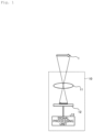
- Fig. 1 is a diagram showing an example of a schematic configuration of an imaging element and an imaging apparatus according to an embodiment.
- An imaging apparatus 10 images an object 1 (subject) by using light from the object 1 as incident light.
- the object 1 is shown as an outlined arrow.
- the incident light is made incident on an imaging element 12 via a lens optical system 11.
- a signal processing unit 13 processes an electric signal from the imaging element 12 to generate an image signal.
- a direction of light incident on the imaging element 12 (an incidence angle to the imaging element 12) differs depending on a position of the imaging element 12.
- Fig. 2 is a diagram showing an example of a schematic configuration of an imaging element.
- an XYZ coordinate system is shown, and an advancing direction of incident light is schematically shown by an arrow.
- a Z-axis direction corresponds to a stacking direction of a PD layer 4 and a transparent layer 5 to be described later.
- An XY planar direction corresponds to a planar direction of these layers.
- a "plan view” indicates viewing in the Z-axis direction (for example, in a Z-axis negative direction) and a “side view” indicates viewing in an X-axis direction or a Y-axis direction (for example, in a Y-axis positive direction).
- Fig. 2 is a cross-sectional view showing an example of a schematic configuration of the imaging element 12 in a side view.
- the imaging element 12 includes a wiring layer 3, a PD (photodiode) layer 4, and a transparent layer 5.
- the PD layer 4 includes a plurality of PD groups 40 which are provided side by side in a planar direction of the layer (which can also be described as being arranged in a two-dimensional direction (in a two-dimensional pattern)).
- Each PD group 40 includes a plurality of PDs provided side by side in the planar direction of the layer.
- the plurality of PDs are formed on a semiconductor substrate 100. Charges generated in each PD are converted into an electric signal which becomes a basis of a pixel signal by transistors (not illustrated) or the like and output to the outside of a pixel 2 through the wiring layer 3.
- Several wirings corresponding to each PD are illustrated as wirings 30.
- the transparent layer 5 is an optical element that disperses incident light toward each of the photoelectric conversion elements of the plurality of PD groups 40.
- An example of the optical element is a meta-surface, and a case where the transparent layer 5 is a meta-surface will be described below.
- the meta-surface is an element which is made up of a plurality of microstructures having a width equal to or less than a wavelength of light and which may have a two-dimensional structure or a three-dimensional structure.
- the transparent layer 5 is provided so as to face the PD layer 4, and in this example, the transparent layer 5 is provided on an upper surface (a surface on a Z-axis positive direction side) of the PD layer 4.
- the transparent layer 5 extends with a planar direction of the PD layer 4 as a planar direction of the layer.
- the transparent layer 5 includes a plurality of structure groups 50 arranged in a planar direction of the layer. In the example shown in Fig.
- the plurality of structure groups 50 are provided inside the transparent layer 5. However, the plurality of structure groups 50 may be provided on the transparent layer 5. The plurality of structure groups 50 may be provided on a lower surface of a transparent substrate and, in such a case, the transparent layer 5 is an air layer.
- the structure constituting the plurality of structure groups 50 is a microstructure having a dimension more or less equal to or smaller than the wavelength (nano-order) of incident light.
- a portion of the transparent layer 5 where the structure is not provided may have a refractive index lower than that of the structure.
- An example of a material of such a transparent layer 5 is SiO 2 .
- the transparent layer 5 may be a void and, in such a case, the refractive index of the transparent layer 5 is the refractive index of air.
- the angle of incident light to the imaging element 12 varies depending on the position on the imaging element 12.
- the incidence angle of light to the transparent layer 5 varies depending on two-dimensional positions (positions on the XY plane).
- the incidence angle in a two-dimensional central portion (hereinafter, also simply referred to as a "central portion") is 0° in this example and, therefore, the light enters the transparent layer 5 perpendicularly.
- an incidence angle in a two-dimensional outer peripheral portion (hereinafter, also simply referred to as an "outer peripheral portion”) deviates from the incidence angle in the central portion. The deviation of the incidence angle becomes larger from the central portion toward the outer peripheral portion.
- Figs. 3 and 4 are diagrams showing an example of a schematic configuration of an imaging element in the central portion.
- Fig. 3 is a cross-sectional view showing an example of a schematic configuration of the imaging element 12 in a side view.
- Fig. 4 is a diagram showing an example of a schematic configuration of the imaging element 12 in a plan view. Since the PD group 40 is located on a lower side (a Z-axis negative direction side) of the structure group 50, the PD group 40 is indicated by a broken line in Fig. 4 .
- a PD 41, a PD 42, and a PD 43 are exemplified.
- the PD 41, the PD 42 and the PD 43 are provided in order in a planar direction of the PD layer 4 (in this example, in the X-axis direction) . It is assumed that light of a wavelength band in accordance with a corresponding color is incident on the PD 41, the PD 42, and the PD 43.
- the PD 41, the PD 42, and the PD 43 correspond to red (R), green (G), and blue (B).
- a structure 51, a structure 52, and a structure 53 are exemplified as a plurality of structures included in the structure group 50.
- the structure 51, the structure 52, and the structure 53 are a plurality of structures each arranged in a same pattern.
- the same pattern means that, for example, a size (width) of each structure and intervals in the planar direction of the transparent layer 5 are the same.
- the size (height) of each structure in the lamination direction may be the same.
- the structure 51, the structure 52, and the structure 53 are arranged so as to disperse incident light respectively toward the PD 41, the PD 42, and the PD 43 of the corresponding PD group 40.
- the structure 51, the structure 52, and the structure 53 are arranged to disperse incident light toward centers of each of the PD 41, the PD 42, and the PD 43.
- the incident light is dispersed into, for example, light of a wavelength band corresponding to each color of RGB as described above, and reaches the PD 41, the PD 42, and the PD 43 corresponding to each color.
- the center of the structure group 50 is located above the center of the PD group 40 (in this example, on the center of the PD 42).
- a principle of spectroscopy by the structure 51, the structure 52, and the structure 53 will be described with reference to Figs. 5 and 6 .
- the structure 51 will be described as an example.
- the structure 52 and the structure 53 can also be described in the same manner.
- Figs. 5 and 6 are diagrams showing an example of a schematic configuration of a structure.
- Fig. 5 shows an example of a plan view (top view) of the structure 51.
- Fig. 6 shows an example of a side view of the structure 51.
- the structure 51 is a fine columnar structure.
- the structure 51 is made of a material such as SiN which has a refractive index n 1 that is higher than a refractive index no of other portions of the transparent layer 5, and a thickness h (a length in the Z-axis direction) of the structure is constant.
- a bottom surface and a top surface of the structure 51 are square.
- the structure 51 acts as an optical waveguide for trapping light inside the structure and propagating the light therein due to a difference in the refractive indexes described above. Accordingly, when light enters from an upper surface side, the light is propagated while being strongly confined inside the structure 51, and the light is subjected to an optical phase delay effect determined by an effective refractive index n eff of the optical waveguide and exits from the bottom surface side.
- n eff is a function of a structural dimension and takes a value that satisfies n 0 ⁇ n eff ⁇ n 1 . Therefore, by changing the width W of the structure 51, an arbitrary optical phase delay amount can be set. An arbitrary optical phase delay amount can also be set by changing the refractive index of the structure 51. Structures 51 having different refractive indices may be made of materials having different refractive indices. This applies likewise to the structure 52 and the structure 53.
- the structure 51, the structure 52, and the structure 53 have different widths so as to give light having been transmitted through the structure group 50 a different optical phase delay distribution for each wavelength region to change an optical wavefront. Since an outgoing direction (propagation direction) of the light is determined by the optical wavefront, the light transmitted through the structure group 50 is spatially separated according to the corresponding colors (wavelength bands) of the PD 41, the PD 42, and the PD 43. In this way, incident light is dispersed toward the PD 41, the PD 42, and the PD 43, respectively.
- the relationship between an incidence angle and an outgoing angle of light in each of the structure groups 50 is also the same.
- the outgoing angle is also different.
- the outgoing angle of the light emitted from the transparent layer 5 toward the PD layer 4 is also deviated.
- the outgoing angle is deviated, light can no longer be efficiently guided to the PD 41, the PD 42, and the PD 43 of the corresponding PD group 40. Therefore, in the imaging element 12, the relative positions of the PD group 40 and the structure group 50 are determined in correspondence to the deviation of the incidence angle (or an outgoing angle attributable thereto).
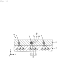
- Fig. 7 and Fig. 8 are diagrams showing an example of a schematic configuration of an imaging element in an outer peripheral portion.
- Fig. 7 is a cross-sectional view showing an example of a schematic configuration of the imaging element 12 in a side view.
- Fig. 8 is a diagram showing an example of a schematic configuration of the imaging element 12 in a plan view.
- an incidence angle of light incident on the structure group 50 is deviated from the incidence angle ( Fig. 3 ) in the central portion. Due to the deviation of the incidence angle, an outgoing angle of light emitted from the structure group 50 toward the PD group 40 is also deviated. However, the relative positions of the PD group 40 and the structure group 50 are also deviated from the relative positions ( Fig. 3 and Fig. 4 ) in the central portion.
- the position of the structure group 50 with respect to the PD group 40 is shifted to a side of the PD 41 of the PD group 40 and, specifically, a center position of the structure group 50 is positioned above a portion on a side of the PD 41 (in this example, above the PD 41) of the PD group 40.
- a direction (angle) in which the PD group 40 is viewed from the structure group 50 is also deviated by the amount of deviation of the relative positions of the PD group 40 and the structure group 50.
- the relative positions of the PD group 40 and the structure group 50 are determined so that the deviation of the direction (angle) in which the PD group 40 is viewed from the structure group 50 cancels out the deviation of the outgoing angle described above.
- the structure group 50 disperses incident light toward the center of each of the PD 41, the PD 42, and the PD 43.
- Fig. 9 is a diagram showing a comparative example.
- the relative positions of the PD group 40 and a structure group 50E are the same as the relative positions in the central portion.
- the light dispersed by a structure 51E, a structure 52E, and a structure 53E reaches a position separated from the center of each of the PD 41, the PD 42, and the PD 43 by an amount of deviation of an outgoing angle attributable to a deviation of an incidence angle.
- this problem is reduced or eliminated by the imaging element 12 according to the embodiment.
- Fig. 10 and Fig. 11 are diagrams showing an example of a schematic configuration of an imaging element in an intermediate portion.
- the intermediate portion is a portion between the central portion and the outer peripheral portion.
- Fig. 10 is a cross-sectional view showing an example of a schematic configuration of the imaging element 12 in a side view.
- Fig. 11 is a diagram showing an example of a schematic configuration of the imaging element 12 in a plan view.
- a deviation of an incidence angle is smaller than a deviation ( Fig. 7 ) of the incidence angle in the outer peripheral portion.
- a deviation of an outgoing angle that is attributable to the deviation of the incidence angle is also smaller than a deviation of the outgoing angle in the outer peripheral portion. Therefore, the deviation of the relative positions of the PD group 40 and the structure group 50 is also smaller than the deviation of the relative positions in the outer peripheral portion.
- the structure group 50 disperses incident light toward the center of each of the PD 41, the PD 42, and the PD 43.
- the relative positions of the corresponding PD group 40 and the structure group 50 differ according to two-dimensional positions (positions with an XY-planer shape). More specifically, when relative positions of the PD group 40 and the structure group 50 in the central portion are used as a benchmark, the relative positions deviate more toward the outer peripheral portion. Supposing that the relative positions are the same at any position, the light dispersed by the structure group 50 reaches a position away from the center of each of the PD 41, the PD 42, and the PD 43 as described earlier with reference to Fig. 9 .
- the signal processing unit 13 of the imaging apparatus 10 will be described.
- the signal processing unit 13 generates a pixel signal based on an electrical signal obtained from the imaging element 12.
- the signal processing unit 13 also controls the imaging element 12.
- the control of the imaging element 12 includes exposure of the pixel 2 of the imaging element 12, conversion of an electric charge accumulated in the PD layer 4 into an electric signal, reading of the electric signal, and the like.
- the incidence angle itself of the light incident on the transparent layer 5 in the outer peripheral portion and the intermediate portion may be made to approach the incidence angle in the central portion. This method will be described with reference to Figs. 12 to 16 .
- Fig. 12 is a diagram showing an example of a schematic configuration of the imaging element in the central portion.
- An exemplified imaging element 12A differs from the imaging element 12 ( Fig. 3 and the like) in that the imaging element 12A includes a transparent layer 5A in place of the transparent layer 5 and further includes a plurality of lenses 61.
- the transparent layer 5A includes a plurality of structure groups 50A.
- Each of the plurality of lenses 61 is a microlens provided for each of the plurality of structure groups 50A.
- the lens 61 has a shape in accordance with a two-dimensional position. In this example, the lens 61 does not change the direction of incident light.
- a structure 51A, a structure 52A, and a structure 53A of the structure group 50A are arranged so as to disperse light from the lens 61 toward the center of each of the PD 41, the PD 42, and the PD 43.
- An incidence angle of light incident on the structure group 50A in the outer peripheral portion and the intermediate portion is deviated from the incidence angle ( Fig. 12 ) in the central portion.
- two methods will be described.
- the principle of shifting the position of a structure group with respect to a PD group described heretofore is also applied to the plurality of lenses 61. The first method will now be described with reference to Figs. 13 and 14 .
- Fig. 13 is a diagram showing an example of a schematic configuration of the imaging element in the outer peripheral portion.
- the relative positions of the plurality of lenses 61 and the structure group 50 are deviated from the relative positions in the central portion.
- the positions of the plurality of lenses 61 with respect to the structure group 50A are shifted to a side of the PD 41 of the PD group 40.
- the lens 61 is arranged so that an incidence angle of light toward the structure group 50A approaches an incidence angle in the central portion.
- the structure 51A, the structure 52A, and the structure 53A of the structure group 50A are arranged so as to disperse light from the lens 62 toward the center of each of the PD 41, the PD 42, and the PD 43.
- Fig. 14 is a diagram showing an example of a schematic configuration of the imaging element in the intermediate portion.
- the relative positions of the plurality of lenses 61 and the structure group 50 are deviated from the relative positions in the central portion. This deviation is smaller than the deviation in the outer peripheral portion ( Fig. 13 ).
- the lens 61 is arranged so that an incidence angle of light toward the structure group 50A approaches an incidence angle in the central portion.
- the structure 51A, the structure 52A, and the structure 53A of the structure group 50A are arranged so as to disperse light from the lens 62 toward the center of each of the PD 41, the PD 42, and the PD 43.
- the second method is a method of providing a lens having a shape in accordance with a two-dimensional position. This method will be described with reference to Figs. 15 and 16 .
- Fig. 15 is a diagram showing an example of a schematic configuration of the imaging element in the outer peripheral portion.
- the imaging element 12A is provided with a plurality of lenses 62 in place of the plurality of lenses 61 in comparison with the central portion ( Fig. 12 ).
- Each of the plurality of lenses 62 is a microlens provided for each of the plurality of structure groups 50A.
- the lens 62 is configured so that an incidence angle of light toward the structure group 50 approaches an incidence angle in the central portion.
- the lens 62 has a shape in accordance with a two-dimensional position which is a shape having been deformed from the shape of the lens 61 ( Fig. 12 ).
- the structure 51A, the structure 52A, and the structure 53A of the structure group 50A are arranged so as to disperse light from the lens 62 toward the center of each of the PD 41, the PD 42, and the PD 43.
- Fig. 16 is a diagram showing an example of a schematic configuration of the imaging element in the intermediate portion.
- the imaging element 12A is provided with a plurality of lenses 63 in place of the plurality of lenses 61 in comparison with the central portion ( Fig. 12 ) .
- Each of the plurality of lenses 63 is a microlens provided for each of the plurality of structure groups 50A.
- the lens 63 is configured so that an incidence angle of light toward the structure group 50 approaches an incidence angle in the central portion.
- the lens 63 has a shape in accordance with a two-dimensional position which is a shape having been deformed from the shape of the lens 61 ( Fig. 12 ) .
- the degree of the deformation is smaller than the degree of deformation of the lens 62 ( Fig. 15 ).
- the structure 51A, the structure 52A, and the structure 53A of the structure group 50A are arranged so as to disperse light from the lens 63 toward the center of each of the PD 41, the PD
- an incidence angle of light incident on the transparent layer 5 in the outer peripheral portion and the intermediate portion can be made to approach an incidence angle in the central portion. Therefore, for example, light is more easily dispersed toward the center of each of the PD 41, the PD 42, and the PD 43 of the PD group 40 than when only the plurality of structure groups 50A are used.
- each structure group 50A disperses light toward the center of each of the PD 41, the PD 42 and the PD 43.
- a reflection suppression layer may be provided to suppress reflection of incident light to the PDs. This method will be described with reference to Figs. 17 and 18 .
- Fig. 17 is a diagram showing an example of a schematic configuration of an imaging element.
- An exemplified imaging element 12B differs from the imaging element 12 ( Fig. 2 ) in that the imaging element 12B further includes a reflection suppression layer 7.
- the reflection suppression layer 7 is provided so as to cover the PD layer 4 and suppresses reflection of light incident on the PD layer 4.
- the reflection suppressing layer 7 is provided between the PD layer 4 and the transparent layer 5.
- the reflection suppressing layer 7 includes a plurality of diffraction gratings 70.
- the plurality of diffraction gratings 70 are periodically arranged in a planar direction of the reflection suppression layer 7.
- the plurality of diffraction gratings 70 have an effective refractive index that differs from the refractive index of the PD layer 4.
- the effective refractive index is a value of the refractive index when it is assumed that the diffraction grating gives a virtual refractive index, in which case the reflection suppressing layer 7 functions as a portion (or a material, a member, or the like) having the effective refractive index.
- the effective refractive index is determined by a grating period (arrangement intervals of the diffraction gratings 70 in the XY-planar direction), a grating height (the length of the diffraction gratings 70 in the Z-axis direction), and the like.
- the grating period may be set equal to or less than the wavelength of the incident light.
- Examples of a material of the diffraction gratings 70 include resins such as plastic, glass, and the like.
- the diffraction grating 70 has an effective refractive index of a magnitude between the refractive index of the PD layer 4 and the refractive index of a portion opposite to the PD layer 4 across the diffraction grating 70. Since the PD layer 4 is formed on the semiconductor substrate 100, the refractive index of the PD layer 4 may be the same as that of the semiconductor substrate 100. In this example, the refractive index of the portion on the opposite side is the refractive index of the transparent layer 5.
- the reflection suppression layer 7 reduces discontinuity between the refractive index of the PD layer 4 and the refractive index of the transparent layer 5 and suppresses reflection of light incident on the PD layer 4.
- Providing the reflection suppressing layer 7 as shown in Fig. 17 enables reflection of light to be suppressed and enables light to be incident on the PD 41, the PD 42 and the PD 43 in an efficient manner.
- the reflection suppressing layer 7 is used together with the transparent layer 5 that includes the plurality of structure groups 50
- the plurality of structure groups 50 need not be provided.
- various known spectroscopic elements may be used instead of the structure groups 50.
- a specific PD may not be covered with the diffraction grating 70.
- An example of the specific PD is a PD which is located immediately below the structure group 50 and on which light from the structure group 50 is vertically incident.
- Such a specific PD may be covered with a reflection suppression film instead of the diffraction grating 70. This configuration will be described with reference to Fig. 18 .
- Fig. 18 is a diagram showing an example of a schematic configuration of an imaging element in a specific PD portion.
- An exemplified imaging element 12B-2 differs from the imaging element 12B ( Fig. 17 ) in that the imaging element 12B-2 includes a reflection suppression layer 7A instead of the reflection suppression layer 7.
- the reflection suppression layer 7A includes a reflection suppression film 71 in addition to a plurality of diffraction gratings 70A.
- the plurality of diffraction gratings 70A cover the PD 41 and the PD 43 while the PD 42 is not covered but exposed. Since the configuration of the diffraction grating 70A is the same as that of the diffraction grating 70, a description thereof will not be repeated.
- the reflection suppression film 71 is provided so as to cover the exposed PD 42 in a gapless manner.
- the reflection suppression film 71 has a refractive index that differ from that of the PD group 40.
- the PD 42 is a photoelectric conversion element corresponding to, for example, green (G). Examples of a material of the reflection suppressing film 71 include resins such as plastic, glass, or the like.
- a reflection suppression amount can be adjusted for each of the PD 41, the PD 42, and the PD 43.
- the plurality of structure groups 50 may be provided on the surface on the transparent layer 5 (for example, on a surface on the Z-axis positive direction side).
- SiN and TiO 2 have been cited as materials for the structure 51 and the like in the embodiment described above, materials are not limited thereto.
- SiN, SiC, TiO 2 , GaN, and the like may be used as materials for the structure 51 and the like with respect to light (visible light to near-infrared light) with a wavelength ranging from 380 nm to 1000 nm. These materials are suitable due to their high refractive index and a small absorption loss.
- Si, SiC, SiN, TiO 2 , GaAs, GaN, and the like may be used as materials for the structure 51 and the like with respect to light (near-infrared light) with a wavelength ranging from 800 nm to 1000 nm.
- InP or the like can be used as a material of the structure 51 or the like in addition to the materials described above.
- examples of materials include a polyimide such as fluorinated polyimide, BCB (benzocyclobutene), a photocurable resin, a UV epoxy resin, an acrylic resin such as PMMA, and a polymer such as a general resist.
- a polyimide such as fluorinated polyimide, BCB (benzocyclobutene)
- a photocurable resin such as fluorinated polyimide, BCB (benzocyclobutene)
- a UV epoxy resin such as an acrylic resin such as PMMA
- a polymer such as a general resist.
- materials of the transparent layer 5 are not limited thereto. Any material including a general glass material may be used as long as a refractive index of the material is smaller than that of the refractive index of the material of the structure 51 and the like and has low loss with respect to the wavelength of incident light.
- the transparent layer 5 may be a transparent layer having a laminated structure made up of a plurality of materials. Furthermore, since a transparent layer 60 need only have sufficiently low loss with respect to a wavelength which is to reach a corresponding PD, the transparent layer 60 may be made of a same material as that of a color filter or made of an organic material such as a resin.
- the PD 41, the PD 42, and the PD 43 may correspond to light (for example, infrared light or ultraviolet light) having wavelengths other than the three primary colors.
- one PD group 40 may include two or four or more PDs. These PDs may be arranged in a one-dimensional direction (for example, in the X-axis direction or the Y-axis direction) or in a two-dimensional direction (for example, in the X-axis direction and the Y-axis direction) .
- an imaging element 12 includes a plurality of PD groups 40, a transparent layer 5, and a plurality of structure groups 50.
- Each of the plurality of PD groups 40 includes a PD 41, a PD 42, and a PD 43 and is arranged in a two-dimensional direction (an XY planar direction).
- the transparent layer 5 faces the plurality of PD groups 40 and extends with a two-dimensional direction as a planar direction.
- the plurality of structure groups 50 are arranged on the transparent layer 5 or in the transparent layer 5 in a planar direction of the transparent layer 5 corresponding to the plurality of PD groups 40.
- Each of the plurality of structure groups 50 includes a structure 51, a structure 52, and a structure 53 arranged in the same pattern, and is arranged so as to disperse incident light toward each of the PD 41, the PD 42, and the PD 43 of the corresponding PD group 40.
- the relative positions of the corresponding PD group 40 and the structure group 50 differ according to two-dimensional positions (positions on an XY plane).
- the relative positions of the corresponding PD group 40 and the structure group 50 differ according to two-dimensional positions. Assuming that the relative positions are the same at any two-dimensional position, as described earlier with reference to Fig. 9 , light dispersed by the structure group 50 reaches a position away from the center of each of the PD 41, the PD 42, and the PD 43. As a result, light is not efficiently incident on the PD 41, the PD 42, and the PD 43 and, for example, problems such as deterioration of light-receiving sensitivity arise.
- the imaging element 12 by shifting relative positions of the corresponding PD group 40 and the structure group 50, a spectral direction by the structure group 50 can be brought close to the center of each of the PD 41, the PD 42, and the PD 43. Therefore, light-receiving sensitivity can be improved.
- a deviation of the relative position may become larger toward a two-dimensional outer peripheral portion.
- a relative position corresponding to the deviation of the incidence angle which becomes larger toward the outer peripheral portion can be determined.
- the structure 51, the structure 52 and the structure 53 are columnar structures having a refractive index that is higher than a refractive index of portions therebetween, at least some structures among the structure 51, the structure 52, and the structure 53 have widths that differ from each other in a plan view, and the structure 51, the structure 52, and the structure 53 may have a same height in a side view. At least some structures among the structure 51, the structure 52, and the structure 53 may have different refractive indices from each other.
- the structure group 50 (the transparent layer 5) can be equipped with a spectroscopic function and incident light can be dispersed toward the PD 41, the PD 42 and the PD 43, respectively.
- the structures can be manufactured more easily than, for example, a case where a plurality of structures having different heights are provided.
- the imaging element 12A includes a plurality of lenses 61 each provided so as to correspond to each of a plurality of structure groups 50A, and relative positions of the corresponding structure groups 50A and the lenses 61 may differ according to two-dimensional positions in a plan view.
- the imaging element 12A may include a lens 61, a lens 62, and a lens 63, each of which is provided with respect to each of the plurality of structure groups 50A and which has a shape in accordance with a two-dimensional position. Therefore, an incidence angle of light that is incident on the transparent layer 5A in the outer peripheral portion and the intermediate portion can be made to approach an incidence angle in the central portion. For example, light is more easily dispersed toward the center of each of the PD 41, the PD 42, and the PD 43 of the PD group 40 than when only the plurality of structure groups 50 are used.
- the imaging element 12B may include a plurality of diffraction gratings 70 which are periodically provided so as to cover at least a part of the plurality of PD groups 40 and which have an effective refractive index with a magnitude that differs from the refractive index of the plurality of PD groups 40. Accordingly, reflection of light is suppressed and light can be made incident on the PD 41, the PD 42 and the PD 43 in an efficient manner.
- the plurality of diffraction gratings 70 expose the PD 42 among the PD 41, the PD 42, and the PD 43 included in each of the plurality of PD groups 40 without covering the PD 42
- the imaging element 12 may include a reflection suppression film 71 which is provided so as to cover the exposed PD 42 in a gapless manner and which has a refractive index that differs from the refractive index of the plurality of PD groups 40.
- the reflection suppressing layer 7A including the two kinds of reflection suppression members namely, the plurality of diffraction gratings 70 and the reflection suppression film 71
- a reflection suppressing amount can be adjusted for each of the PD 41, the PD 42 and the PD 43.
- the imaging apparatus 10 described with reference to Fig. 1 and the like is also an aspect of the present disclosure.
- the imaging apparatus 10 includes an imaging element 12 and a signal processing unit 13 for generating an image signal on the basis of an electric signal obtained from the imaging element 12. Accordingly, the imaging apparatus 10 capable of improving light-receiving efficiency can be obtained.
Abstract
Description
- The present disclosure relates to an imaging element and an imaging apparatus.
- In an imaging apparatus, incidence angles of light are known to differ between a central portion and an outer peripheral portion of an imaging element (for example, refer to PTL 1).
- [PTL 1]
Japanese National Publication of International Patent Application No. 2006-528424 - There is a problem in that, when an incidence angle deviates, light cannot be efficiently guided to a conversion element and light-receiving efficiency decreases.
- An aspect of the present disclosure is to enable light-receiving efficiency to be improved.
- An imaging element according to an aspect of the present disclosure includes: a plurality of photoelectric conversion element groups each including a plurality of photoelectric conversion elements and being arranged in a two-dimensional direction; a transparent layer which faces the plurality of photoelectric conversion element groups and which extends in the two-dimensional direction as a planar direction; and a plurality of structure groups arranged in a planar direction of the transparent layer so as to correspond to the plurality of photoelectric conversion element groups on the transparent layer or inside the transparent layer, wherein each of the plurality of structure groups includes a plurality of structures arranged in a same pattern and is arranged so as to disperse incident light toward each of the photoelectric conversion elements of a corresponding photoelectric conversion element group, and in a plan view, relative positions of the corresponding photoelectric conversion element group and a structure group differ according to two-dimensional positions.
- An imaging apparatus according to an aspect of the present disclosure includes the imaging element described above and a signal processing unit configured to generate an image signal based on an electric signal obtained from the imaging element.
- According to the present disclosure, light-receiving efficiency can be improved.
-
- [
Fig. 1 ]
Fig. 1 is a diagram showing an example of a schematic configuration of an imaging element and an imaging apparatus according to an embodiment. - [
Fig. 2 ]
Fig. 2 is a diagram showing an example of a schematic configuration of an imaging element. - [
Fig. 3 ]
Fig. 3 is a diagram showing an example of a schematic configuration of an imaging element in a central portion. - [
Fig. 4 ]
Fig. 4 is a diagram showing an example of a schematic configuration of an imaging element in a central portion. - [
Fig. 5 ]
Fig. 5 is a diagram showing an example of a schematic configuration of a structure. - [
Fig. 6 ]
Fig. 6 is a diagram showing an example of a schematic configuration of a structure. - [
Fig. 7 ]
Fig. 7 is a diagram showing an example of a schematic configuration of an imaging element in an outer peripheral portion. - [
Fig. 8 ]
Fig. 8 is a diagram showing an example of a schematic configuration of an imaging element in an outer peripheral portion. - [
Fig. 9 ]
Fig. 9 is a diagram showing a comparative example. - [
Fig. 10 ]
Fig. 10 is a diagram showing an example of a schematic configuration of an imaging element in an intermediate portion. - [
Fig. 11 ]
Fig. 11 is a diagram showing an example of a schematic configuration of an imaging element in an intermediate portion. - [
Fig. 12 ]
Fig. 12 is a diagram showing an example of a schematic configuration of an imaging element in a central portion. - [
Fig. 13 ]
Fig. 13 is a diagram showing an example of a schematic configuration of an imaging element in an outer peripheral portion. - [
Fig. 14 ]
Fig. 14 is a diagram showing an example of a schematic configuration of an imaging element in an intermediate portion. - [
Fig. 15 ]
Fig. 15 is a diagram showing an example of a schematic configuration of an imaging element in an outer peripheral portion. - [
Fig. 16 ]
Fig. 16 is a diagram showing an example of a schematic configuration of an imaging element in an intermediate portion. - [
Fig. 17 ]
Fig. 17 is a diagram showing an example of a schematic configuration of an imaging element. - [
Fig. 18 ]
Fig. 18 is a diagram showing an example of a schematic configuration of an imaging element in a portion of a specific PD. - Hereinafter, an embodiment of the present invention will be described with reference to the accompanying drawings . It is to be understood that shapes, sizes, positional relationships, and the like shown in the drawings are merely schematic and the present invention is not limited thereto. Same portions will be denoted by same reference signs and redundant descriptions will be omitted.
-
Fig. 1 is a diagram showing an example of a schematic configuration of an imaging element and an imaging apparatus according to an embodiment. Animaging apparatus 10 images an object 1 (subject) by using light from theobject 1 as incident light. In this example, theobject 1 is shown as an outlined arrow. The incident light is made incident on animaging element 12 via a lensoptical system 11. Asignal processing unit 13 processes an electric signal from theimaging element 12 to generate an image signal. As shown inFig. 1 , a direction of light incident on the imaging element 12 (an incidence angle to the imaging element 12) differs depending on a position of theimaging element 12. -
Fig. 2 is a diagram showing an example of a schematic configuration of an imaging element. In the diagram, an XYZ coordinate system is shown, and an advancing direction of incident light is schematically shown by an arrow. A Z-axis direction corresponds to a stacking direction of aPD layer 4 and atransparent layer 5 to be described later. An XY planar direction corresponds to a planar direction of these layers. - Hereinafter, a "plan view" indicates viewing in the Z-axis direction (for example, in a Z-axis negative direction) and a "side view" indicates viewing in an X-axis direction or a Y-axis direction (for example, in a Y-axis positive direction).
Fig. 2 is a cross-sectional view showing an example of a schematic configuration of theimaging element 12 in a side view. - The
imaging element 12 includes a wiring layer 3, a PD (photodiode)layer 4, and atransparent layer 5. - To first describe the
PD layer 4 among the wiring layer 3 and thePD layer 4, thePD layer 4 includes a plurality ofPD groups 40 which are provided side by side in a planar direction of the layer (which can also be described as being arranged in a two-dimensional direction (in a two-dimensional pattern)). EachPD group 40 includes a plurality of PDs provided side by side in the planar direction of the layer. The plurality of PDs are formed on asemiconductor substrate 100. Charges generated in each PD are converted into an electric signal which becomes a basis of a pixel signal by transistors (not illustrated) or the like and output to the outside of apixel 2 through the wiring layer 3. Several wirings corresponding to each PD are illustrated aswirings 30. - The
transparent layer 5 is an optical element that disperses incident light toward each of the photoelectric conversion elements of the plurality of PD groups 40. An example of the optical element is a meta-surface, and a case where thetransparent layer 5 is a meta-surface will be described below. The meta-surface is an element which is made up of a plurality of microstructures having a width equal to or less than a wavelength of light and which may have a two-dimensional structure or a three-dimensional structure. By using a meta-surface for the optical element, a phase and light intensity can be controlled according to characteristics (wavelength, polarization, and incidence angle) of light by merely changing a parameter of the microstructures, and the degree of freedom in design described above is increased in the case of forming a three-dimensional structure. Thetransparent layer 5 is provided so as to face thePD layer 4, and in this example, thetransparent layer 5 is provided on an upper surface (a surface on a Z-axis positive direction side) of thePD layer 4. Thetransparent layer 5 extends with a planar direction of thePD layer 4 as a planar direction of the layer. Thetransparent layer 5 includes a plurality ofstructure groups 50 arranged in a planar direction of the layer. In the example shown inFig. 2 , the plurality ofstructure groups 50 are provided inside thetransparent layer 5. However, the plurality ofstructure groups 50 may be provided on thetransparent layer 5. The plurality ofstructure groups 50 may be provided on a lower surface of a transparent substrate and, in such a case, thetransparent layer 5 is an air layer. The structure constituting the plurality ofstructure groups 50 is a microstructure having a dimension more or less equal to or smaller than the wavelength (nano-order) of incident light. - A portion of the
transparent layer 5 where the structure is not provided may have a refractive index lower than that of the structure. An example of a material of such atransparent layer 5 is SiO2. Thetransparent layer 5 may be a void and, in such a case, the refractive index of thetransparent layer 5 is the refractive index of air. - As described earlier with reference to
Fig. 1 , the angle of incident light to theimaging element 12 varies depending on the position on theimaging element 12. In the example shown inFig. 2 , the incidence angle of light to thetransparent layer 5 varies depending on two-dimensional positions (positions on the XY plane). In theimaging element 12, the incidence angle in a two-dimensional central portion (hereinafter, also simply referred to as a "central portion") is 0° in this example and, therefore, the light enters thetransparent layer 5 perpendicularly. In theimaging element 12, an incidence angle in a two-dimensional outer peripheral portion (hereinafter, also simply referred to as an "outer peripheral portion") deviates from the incidence angle in the central portion. The deviation of the incidence angle becomes larger from the central portion toward the outer peripheral portion. -
Figs. 3 and4 are diagrams showing an example of a schematic configuration of an imaging element in the central portion.Fig. 3 is a cross-sectional view showing an example of a schematic configuration of theimaging element 12 in a side view.Fig. 4 is a diagram showing an example of a schematic configuration of theimaging element 12 in a plan view. Since thePD group 40 is located on a lower side (a Z-axis negative direction side) of thestructure group 50, thePD group 40 is indicated by a broken line inFig. 4 . - As a plurality of diodes included in the
PD group 40, aPD 41, aPD 42, and aPD 43 are exemplified. ThePD 41, thePD 42 and thePD 43 are provided in order in a planar direction of the PD layer 4 (in this example, in the X-axis direction) . It is assumed that light of a wavelength band in accordance with a corresponding color is incident on thePD 41, thePD 42, and thePD 43. For example, thePD 41, thePD 42, and thePD 43 correspond to red (R), green (G), and blue (B). - A
structure 51, astructure 52, and astructure 53 are exemplified as a plurality of structures included in thestructure group 50. Thestructure 51, thestructure 52, and thestructure 53 are a plurality of structures each arranged in a same pattern. The same pattern means that, for example, a size (width) of each structure and intervals in the planar direction of thetransparent layer 5 are the same. The size (height) of each structure in the lamination direction may be the same. Thestructure 51, thestructure 52, and thestructure 53 are arranged so as to disperse incident light respectively toward thePD 41, thePD 42, and thePD 43 of the correspondingPD group 40. More specifically, thestructure 51, thestructure 52, and thestructure 53 are arranged to disperse incident light toward centers of each of thePD 41, thePD 42, and thePD 43. The incident light is dispersed into, for example, light of a wavelength band corresponding to each color of RGB as described above, and reaches thePD 41, thePD 42, and thePD 43 corresponding to each color. In the examples shown inFigs. 3 and4 , the center of thestructure group 50 is located above the center of the PD group 40 (in this example, on the center of the PD 42). - A principle of spectroscopy by the
structure 51, thestructure 52, and thestructure 53 will be described with reference toFigs. 5 and6 . Hereinafter, thestructure 51 will be described as an example. Thestructure 52 and thestructure 53 can also be described in the same manner. -
Figs. 5 and6 are diagrams showing an example of a schematic configuration of a structure.Fig. 5 shows an example of a plan view (top view) of thestructure 51.Fig. 6 shows an example of a side view of thestructure 51. - In this example, the
structure 51 is a fine columnar structure. Thestructure 51 is made of a material such as SiN which has a refractive index n1 that is higher than a refractive index no of other portions of thetransparent layer 5, and a thickness h (a length in the Z-axis direction) of the structure is constant. - A bottom surface and a top surface of the
structure 51 are square. Thestructure 51 acts as an optical waveguide for trapping light inside the structure and propagating the light therein due to a difference in the refractive indexes described above. Accordingly, when light enters from an upper surface side, the light is propagated while being strongly confined inside thestructure 51, and the light is subjected to an optical phase delay effect determined by an effective refractive index neff of the optical waveguide and exits from the bottom surface side. - Specifically, when a phase of light having propagated over a length corresponding to the thickness of the
transparent layer 5 is used as a benchmark, an optical phase delay amount φ by thestructure 51 is expressed by φ = (neff - no) × 2 π h/ λ, where λ denotes a wavelength of the light in vacuum. Since the optical phase delay amount differs depending on the wavelength λ, a different optical phase delay amount in accordance with a wavelength band (color) is given to light incident on thesame structure 51. Since the bottom surface and the top surface of thestructure 51 are square, there is no change in optical characteristics including an optical phase delay effect even when a polarization direction is changed. It is known that neff is a function of a structural dimension and takes a value that satisfies n0 < neff < n1. Therefore, by changing the width W of thestructure 51, an arbitrary optical phase delay amount can be set. An arbitrary optical phase delay amount can also be set by changing the refractive index of thestructure 51.Structures 51 having different refractive indices may be made of materials having different refractive indices. This applies likewise to thestructure 52 and thestructure 53. - Referring also to
Figs. 3 and4 , thestructure 51, thestructure 52, and thestructure 53 have different widths so as to give light having been transmitted through the structure group 50 a different optical phase delay distribution for each wavelength region to change an optical wavefront. Since an outgoing direction (propagation direction) of the light is determined by the optical wavefront, the light transmitted through thestructure group 50 is spatially separated according to the corresponding colors (wavelength bands) of thePD 41, thePD 42, and thePD 43. In this way, incident light is dispersed toward thePD 41, thePD 42, and thePD 43, respectively. - Since the
structure 51, thestructure 52, and thestructure 53 are arranged in the same pattern in each of the plurality ofstructure groups 50, the relationship between an incidence angle and an outgoing angle of light in each of thestructure groups 50 is also the same. When the incidence angle is different, the outgoing angle is also different. As described earlier, since the incidence angle in the outer peripheral portion is deviated from the incidence angle in the central portion, the outgoing angle of the light emitted from thetransparent layer 5 toward thePD layer 4 is also deviated. When the outgoing angle is deviated, light can no longer be efficiently guided to thePD 41, thePD 42, and thePD 43 of the correspondingPD group 40. Therefore, in theimaging element 12, the relative positions of thePD group 40 and thestructure group 50 are determined in correspondence to the deviation of the incidence angle (or an outgoing angle attributable thereto). -
Fig. 7 andFig. 8 are diagrams showing an example of a schematic configuration of an imaging element in an outer peripheral portion.Fig. 7 is a cross-sectional view showing an example of a schematic configuration of theimaging element 12 in a side view.Fig. 8 is a diagram showing an example of a schematic configuration of theimaging element 12 in a plan view. - In the outer peripheral portion, an incidence angle of light incident on the
structure group 50 is deviated from the incidence angle (Fig. 3 ) in the central portion. Due to the deviation of the incidence angle, an outgoing angle of light emitted from thestructure group 50 toward thePD group 40 is also deviated. However, the relative positions of thePD group 40 and thestructure group 50 are also deviated from the relative positions (Fig. 3 andFig. 4 ) in the central portion. In this example, the position of thestructure group 50 with respect to thePD group 40 is shifted to a side of thePD 41 of thePD group 40 and, specifically, a center position of thestructure group 50 is positioned above a portion on a side of the PD 41 (in this example, above the PD 41) of thePD group 40. A direction (angle) in which thePD group 40 is viewed from thestructure group 50 is also deviated by the amount of deviation of the relative positions of thePD group 40 and thestructure group 50. The relative positions of thePD group 40 and thestructure group 50 are determined so that the deviation of the direction (angle) in which thePD group 40 is viewed from thestructure group 50 cancels out the deviation of the outgoing angle described above. As a result, even in the outer peripheral portion, thestructure group 50 disperses incident light toward the center of each of thePD 41, thePD 42, and thePD 43. - Supposing that the relative positions of the
PD group 40 and thestructure group 50 in the outer peripheral portion are the same as the relative positions in the central portion, the light dispersed by thestructure group 50 is no longer directed to the center of each of thePD 41, thePD 42, and thePD 43. This state will be described with reference toFig. 9 . -
Fig. 9 is a diagram showing a comparative example. In an exemplifiedimaging element 12E, the relative positions of thePD group 40 and astructure group 50E are the same as the relative positions in the central portion. The light dispersed by astructure 51E, astructure 52E, and astructure 53E reaches a position separated from the center of each of thePD 41, thePD 42, and thePD 43 by an amount of deviation of an outgoing angle attributable to a deviation of an incidence angle. As described earlier with reference toFig. 7 andFig. 8 , this problem is reduced or eliminated by theimaging element 12 according to the embodiment. -
Fig. 10 andFig. 11 are diagrams showing an example of a schematic configuration of an imaging element in an intermediate portion. The intermediate portion is a portion between the central portion and the outer peripheral portion.Fig. 10 is a cross-sectional view showing an example of a schematic configuration of theimaging element 12 in a side view.Fig. 11 is a diagram showing an example of a schematic configuration of theimaging element 12 in a plan view. - . In the intermediate portion, a deviation of an incidence angle is smaller than a deviation (
Fig. 7 ) of the incidence angle in the outer peripheral portion. A deviation of an outgoing angle that is attributable to the deviation of the incidence angle is also smaller than a deviation of the outgoing angle in the outer peripheral portion. Therefore, the deviation of the relative positions of thePD group 40 and thestructure group 50 is also smaller than the deviation of the relative positions in the outer peripheral portion. Also in the intermediate portion, thestructure group 50 disperses incident light toward the center of each of thePD 41, thePD 42, and thePD 43. - As described above, for example, in the
imaging element 12, the relative positions of the correspondingPD group 40 and thestructure group 50 differ according to two-dimensional positions (positions with an XY-planer shape). More specifically, when relative positions of thePD group 40 and thestructure group 50 in the central portion are used as a benchmark, the relative positions deviate more toward the outer peripheral portion. Supposing that the relative positions are the same at any position, the light dispersed by thestructure group 50 reaches a position away from the center of each of thePD 41, thePD 42, and thePD 43 as described earlier with reference toFig. 9 . As a result, light is not efficiently incident on thePD 41, thePD 42, and thePD 43 and, for example, problems such as deterioration of light-receiving sensitivity arise. On the other hand, in theimaging element 12, by shifting relative positions of the correspondingPD group 40 and thestructure group 50, a spectral direction by thestructure group 50 can be brought close to the center of each of thePD 41, thePD 42, and thePD 43. As a result, light-receiving efficiency can be improved. - Once again referring to
Fig. 1 , thesignal processing unit 13 of theimaging apparatus 10 will be described. Thesignal processing unit 13 generates a pixel signal based on an electrical signal obtained from theimaging element 12. In order to obtain an electric signal, thesignal processing unit 13 also controls theimaging element 12. The control of theimaging element 12 includes exposure of thepixel 2 of theimaging element 12, conversion of an electric charge accumulated in thePD layer 4 into an electric signal, reading of the electric signal, and the like. - Although an embodiment of the present disclosure has been described above, the imaging element and the imaging apparatus according to the embodiment can be variously modified without departing from the spirit of the embodiment. Several modifications will now be discussed.
- In the embodiment described above, a method of coping with a problem attributable to a deviation of incident light with relative positions of the
PD group 40 and thestructure group 50 has been described. Other various methods may be used in addition to or in place of this method. - For example, the incidence angle itself of the light incident on the
transparent layer 5 in the outer peripheral portion and the intermediate portion may be made to approach the incidence angle in the central portion. This method will be described with reference toFigs. 12 to 16 . -
Fig. 12 is a diagram showing an example of a schematic configuration of the imaging element in the central portion. An exemplifiedimaging element 12A differs from the imaging element 12 (Fig. 3 and the like) in that theimaging element 12A includes atransparent layer 5A in place of thetransparent layer 5 and further includes a plurality oflenses 61. Thetransparent layer 5A includes a plurality ofstructure groups 50A. - Each of the plurality of
lenses 61 is a microlens provided for each of the plurality ofstructure groups 50A. Thelens 61 has a shape in accordance with a two-dimensional position. In this example, thelens 61 does not change the direction of incident light. Astructure 51A, astructure 52A, and astructure 53A of thestructure group 50A are arranged so as to disperse light from thelens 61 toward the center of each of thePD 41, thePD 42, and thePD 43. - An incidence angle of light incident on the
structure group 50A in the outer peripheral portion and the intermediate portion is deviated from the incidence angle (Fig. 12 ) in the central portion. As an example of a method for reducing this deviation, two methods will be described. In the first method, the principle of shifting the position of a structure group with respect to a PD group described heretofore is also applied to the plurality oflenses 61. The first method will now be described with reference toFigs. 13 and14 . - .
Fig. 13 is a diagram showing an example of a schematic configuration of the imaging element in the outer peripheral portion. As compared with the central portion (Fig. 12 ), the relative positions of the plurality oflenses 61 and thestructure group 50 are deviated from the relative positions in the central portion. In this example, the positions of the plurality oflenses 61 with respect to thestructure group 50A are shifted to a side of thePD 41 of thePD group 40. Thelens 61 is arranged so that an incidence angle of light toward thestructure group 50A approaches an incidence angle in the central portion. Thestructure 51A, thestructure 52A, and thestructure 53A of thestructure group 50A are arranged so as to disperse light from thelens 62 toward the center of each of thePD 41, thePD 42, and thePD 43. -
Fig. 14 is a diagram showing an example of a schematic configuration of the imaging element in the intermediate portion. As compared with the central portion (Fig. 12 ), the relative positions of the plurality oflenses 61 and thestructure group 50 are deviated from the relative positions in the central portion. This deviation is smaller than the deviation in the outer peripheral portion (Fig. 13 ). Thelens 61 is arranged so that an incidence angle of light toward thestructure group 50A approaches an incidence angle in the central portion. Thestructure 51A, thestructure 52A, and thestructure 53A of thestructure group 50A are arranged so as to disperse light from thelens 62 toward the center of each of thePD 41, thePD 42, and thePD 43. - The second method is a method of providing a lens having a shape in accordance with a two-dimensional position. This method will be described with reference to
Figs. 15 and16 . -
Fig. 15 is a diagram showing an example of a schematic configuration of the imaging element in the outer peripheral portion. Theimaging element 12A is provided with a plurality oflenses 62 in place of the plurality oflenses 61 in comparison with the central portion (Fig. 12 ). Each of the plurality oflenses 62 is a microlens provided for each of the plurality ofstructure groups 50A. Thelens 62 is configured so that an incidence angle of light toward thestructure group 50 approaches an incidence angle in the central portion. Thelens 62 has a shape in accordance with a two-dimensional position which is a shape having been deformed from the shape of the lens 61 (Fig. 12 ). Thestructure 51A, thestructure 52A, and thestructure 53A of thestructure group 50A are arranged so as to disperse light from thelens 62 toward the center of each of thePD 41, thePD 42, and thePD 43. -
Fig. 16 is a diagram showing an example of a schematic configuration of the imaging element in the intermediate portion. Theimaging element 12A is provided with a plurality oflenses 63 in place of the plurality oflenses 61 in comparison with the central portion (Fig. 12 ) . Each of the plurality oflenses 63 is a microlens provided for each of the plurality ofstructure groups 50A. Thelens 63 is configured so that an incidence angle of light toward thestructure group 50 approaches an incidence angle in the central portion. Thelens 63 has a shape in accordance with a two-dimensional position which is a shape having been deformed from the shape of the lens 61 (Fig. 12 ) . The degree of the deformation is smaller than the degree of deformation of the lens 62 (Fig. 15 ). Thestructure 51A, thestructure 52A, and thestructure 53A of thestructure group 50A are arranged so as to disperse light from thelens 63 toward the center of each of thePD 41, thePD 42, and thePD 43. - As shown in
Figs. 12 to 16 , by differentiating relative positions of the corresponding plurality oflenses 61 and thestructure group 50 in accordance with the two-dimensional positions or providing thelens 61, thelens 62 and thelens 63 having a shape in accordance with the two-dimensional positions, an incidence angle of light incident on thetransparent layer 5 in the outer peripheral portion and the intermediate portion can be made to approach an incidence angle in the central portion. Therefore, for example, light is more easily dispersed toward the center of each of thePD 41, thePD 42, and thePD 43 of thePD group 40 than when only the plurality ofstructure groups 50A are used. For example, if the incidence angle in the outer peripheral portion and the intermediate portion can be brought sufficiently close to the incidence angle in the central portion using only thelens 61 or the like, the relative positions of thecorresponding structure group 50A and thePD group 40 need not be deviated. This is because eachstructure group 50A disperses light toward the center of each of thePD 41, thePD 42 and thePD 43. - For example, a reflection suppression layer may be provided to suppress reflection of incident light to the PDs. This method will be described with reference to
Figs. 17 and18 . -
Fig. 17 is a diagram showing an example of a schematic configuration of an imaging element. An exemplifiedimaging element 12B differs from the imaging element 12 (Fig. 2 ) in that theimaging element 12B further includes a reflection suppression layer 7. - The reflection suppression layer 7 is provided so as to cover the
PD layer 4 and suppresses reflection of light incident on thePD layer 4. In this example, the reflection suppressing layer 7 is provided between thePD layer 4 and thetransparent layer 5. - In the example shown in
Fig. 17 , the reflection suppressing layer 7 includes a plurality ofdiffraction gratings 70. The plurality ofdiffraction gratings 70 are periodically arranged in a planar direction of the reflection suppression layer 7. The plurality ofdiffraction gratings 70 have an effective refractive index that differs from the refractive index of thePD layer 4. The effective refractive index is a value of the refractive index when it is assumed that the diffraction grating gives a virtual refractive index, in which case the reflection suppressing layer 7 functions as a portion (or a material, a member, or the like) having the effective refractive index. Since a method of realizing a desired effective refractive index by a plurality of periodically-arranged diffraction gratings is known, a brief description will now be given. The effective refractive index is determined by a grating period (arrangement intervals of thediffraction gratings 70 in the XY-planar direction), a grating height (the length of thediffraction gratings 70 in the Z-axis direction), and the like. The grating period may be set equal to or less than the wavelength of the incident light. Examples of a material of thediffraction gratings 70 include resins such as plastic, glass, and the like. - The
diffraction grating 70 has an effective refractive index of a magnitude between the refractive index of thePD layer 4 and the refractive index of a portion opposite to thePD layer 4 across thediffraction grating 70. Since thePD layer 4 is formed on thesemiconductor substrate 100, the refractive index of thePD layer 4 may be the same as that of thesemiconductor substrate 100. In this example, the refractive index of the portion on the opposite side is the refractive index of thetransparent layer 5. Since thediffraction grating 70 has an effective refractive index of a magnitude between the refractive indices, the reflection suppression layer 7 reduces discontinuity between the refractive index of thePD layer 4 and the refractive index of thetransparent layer 5 and suppresses reflection of light incident on thePD layer 4. - Providing the reflection suppressing layer 7 as shown in
Fig. 17 enables reflection of light to be suppressed and enables light to be incident on thePD 41, thePD 42 and thePD 43 in an efficient manner. - Although an example in which the reflection suppressing layer 7 is used together with the
transparent layer 5 that includes the plurality ofstructure groups 50 has been described above, if light can be made incident in a somewhat efficient manner only by the reflection suppressing layer 7, the plurality ofstructure groups 50 need not be provided. In this case, various known spectroscopic elements may be used instead of the structure groups 50. - In the
imaging element 12B described above, a specific PD may not be covered with thediffraction grating 70. An example of the specific PD is a PD which is located immediately below thestructure group 50 and on which light from thestructure group 50 is vertically incident. Such a specific PD may be covered with a reflection suppression film instead of thediffraction grating 70. This configuration will be described with reference toFig. 18 . -
Fig. 18 is a diagram showing an example of a schematic configuration of an imaging element in a specific PD portion. An exemplifiedimaging element 12B-2 differs from theimaging element 12B (Fig. 17 ) in that theimaging element 12B-2 includes areflection suppression layer 7A instead of the reflection suppression layer 7. - The
reflection suppression layer 7A includes areflection suppression film 71 in addition to a plurality of diffraction gratings 70A. The plurality of diffraction gratings 70A cover thePD 41 and thePD 43 while thePD 42 is not covered but exposed. Since the configuration of the diffraction grating 70A is the same as that of thediffraction grating 70, a description thereof will not be repeated. Thereflection suppression film 71 is provided so as to cover the exposedPD 42 in a gapless manner. Thereflection suppression film 71 has a refractive index that differ from that of thePD group 40. ThePD 42 is a photoelectric conversion element corresponding to, for example, green (G). Examples of a material of thereflection suppressing film 71 include resins such as plastic, glass, or the like. - As shown in
Fig. 18 , by using thereflection suppression layer 7A that includes the two kinds of reflection suppression members, namely, the plurality ofdiffraction gratings 70 and thereflection suppression film 71, for example, a reflection suppression amount can be adjusted for each of thePD 41, thePD 42, and thePD 43. - Although an embodiment of the present disclosure has been described above, the imaging element and the imaging apparatus according to the embodiment can be variously modified without departing from the spirit of the embodiment.
- In the above embodiment, an example in which the plurality of
structure groups 50 are provided in thetransparent layer 5 has been described. However, the plurality ofstructure groups 50 may be provided on the surface on the transparent layer 5 (for example, on a surface on the Z-axis positive direction side). - While SiN and TiO2 have been cited as materials for the
structure 51 and the like in the embodiment described above, materials are not limited thereto. For example, SiN, SiC, TiO2, GaN, and the like may be used as materials for thestructure 51 and the like with respect to light (visible light to near-infrared light) with a wavelength ranging from 380 nm to 1000 nm. These materials are suitable due to their high refractive index and a small absorption loss. Si, SiC, SiN, TiO2, GaAs, GaN, and the like may be used as materials for thestructure 51 and the like with respect to light (near-infrared light) with a wavelength ranging from 800 nm to 1000 nm. These materials are suitable due to their low loss. With respect to light in a near-infrared region of a long wavelength band (such as 1.3 µm and 1.55 µm which are communication wavelengths), InP or the like can be used as a material of thestructure 51 or the like in addition to the materials described above. - When the
structure 51 and the like are formed through adhesion, coating, and the like, examples of materials include a polyimide such as fluorinated polyimide, BCB (benzocyclobutene), a photocurable resin, a UV epoxy resin, an acrylic resin such as PMMA, and a polymer such as a general resist. - While an example in which SiO2 and an air layer are assumed as materials of the
transparent layer 5 has been shown in the embodiment described above, materials of thetransparent layer 5 are not limited thereto. Any material including a general glass material may be used as long as a refractive index of the material is smaller than that of the refractive index of the material of thestructure 51 and the like and has low loss with respect to the wavelength of incident light. Thetransparent layer 5 may be a transparent layer having a laminated structure made up of a plurality of materials. Furthermore, since a transparent layer 60 need only have sufficiently low loss with respect to a wavelength which is to reach a corresponding PD, the transparent layer 60 may be made of a same material as that of a color filter or made of an organic material such as a resin. - While the three primary colors of RGB have been described as an example of colors that the
PD 41, thePD 42, and thePD 43 correspond to in the embodiment described above, thePD 41, thePD 42, and thePD 43 may correspond to light (for example, infrared light or ultraviolet light) having wavelengths other than the three primary colors. - While an example in which one
PD group 40 includes three PDs, namely, thePD 41, thePD 42, and thePD 43 has been described in the embodiment described above, one PD group may include two or four or more PDs. These PDs may be arranged in a one-dimensional direction (for example, in the X-axis direction or the Y-axis direction) or in a two-dimensional direction (for example, in the X-axis direction and the Y-axis direction) . - While the present invention has been described based on a specific embodiment, it is obvious that the present invention is not limited to the foregoing embodiment and can be modified in various ways without departing from the spirit of the invention.
- For example, the imaging element described above is specified as follows. As described with reference to
Figs. 1 to 11 and the like, animaging element 12 includes a plurality ofPD groups 40, atransparent layer 5, and a plurality of structure groups 50. Each of the plurality ofPD groups 40 includes aPD 41, aPD 42, and aPD 43 and is arranged in a two-dimensional direction (an XY planar direction). Thetransparent layer 5 faces the plurality ofPD groups 40 and extends with a two-dimensional direction as a planar direction. The plurality ofstructure groups 50 are arranged on thetransparent layer 5 or in thetransparent layer 5 in a planar direction of thetransparent layer 5 corresponding to the plurality of PD groups 40. Each of the plurality ofstructure groups 50 includes astructure 51, astructure 52, and astructure 53 arranged in the same pattern, and is arranged so as to disperse incident light toward each of thePD 41, thePD 42, and thePD 43 of the correspondingPD group 40. In a plan view, the relative positions of the correspondingPD group 40 and thestructure group 50 differ according to two-dimensional positions (positions on an XY plane). - In the
imaging element 12, the relative positions of the correspondingPD group 40 and thestructure group 50 differ according to two-dimensional positions. Assuming that the relative positions are the same at any two-dimensional position, as described earlier with reference toFig. 9 , light dispersed by thestructure group 50 reaches a position away from the center of each of thePD 41, thePD 42, and thePD 43. As a result, light is not efficiently incident on thePD 41, thePD 42, and thePD 43 and, for example, problems such as deterioration of light-receiving sensitivity arise. On the other hand, in theimaging element 12, by shifting relative positions of the correspondingPD group 40 and thestructure group 50, a spectral direction by thestructure group 50 can be brought close to the center of each of thePD 41, thePD 42, and thePD 43. Therefore, light-receiving sensitivity can be improved. - When a relative position in a two-dimensional central portion in the
imaging element 12 is used as a benchmark, a deviation of the relative position may become larger toward a two-dimensional outer peripheral portion. Thus, a relative position corresponding to the deviation of the incidence angle which becomes larger toward the outer peripheral portion can be determined. - As described with reference to
Figs. 5 and6 and the like, thestructure 51, thestructure 52 and thestructure 53 are columnar structures having a refractive index that is higher than a refractive index of portions therebetween, at least some structures among thestructure 51, thestructure 52, and thestructure 53 have widths that differ from each other in a plan view, and thestructure 51, thestructure 52, and thestructure 53 may have a same height in a side view. At least some structures among thestructure 51, thestructure 52, and thestructure 53 may have different refractive indices from each other. For example, by arranging thestructure 51, thestructure 52, and thestructure 53 configured as described above, the structure group 50 (the transparent layer 5) can be equipped with a spectroscopic function and incident light can be dispersed toward thePD 41, thePD 42 and thePD 43, respectively. Furthermore, the structures can be manufactured more easily than, for example, a case where a plurality of structures having different heights are provided. - As described with reference to
Figs. 12 to 14 and the like, theimaging element 12A includes a plurality oflenses 61 each provided so as to correspond to each of a plurality ofstructure groups 50A, and relative positions of thecorresponding structure groups 50A and thelenses 61 may differ according to two-dimensional positions in a plan view. - Alternatively, as described with reference to
Fig. 12 ,Fig. 15 ,Fig. 16 , and the like, theimaging element 12A may include alens 61, alens 62, and alens 63, each of which is provided with respect to each of the plurality ofstructure groups 50A and which has a shape in accordance with a two-dimensional position. Therefore, an incidence angle of light that is incident on thetransparent layer 5A in the outer peripheral portion and the intermediate portion can be made to approach an incidence angle in the central portion. For example, light is more easily dispersed toward the center of each of thePD 41, thePD 42, and thePD 43 of thePD group 40 than when only the plurality ofstructure groups 50 are used. - As described with reference to
Fig. 17 and the like, theimaging element 12B may include a plurality ofdiffraction gratings 70 which are periodically provided so as to cover at least a part of the plurality ofPD groups 40 and which have an effective refractive index with a magnitude that differs from the refractive index of the plurality of PD groups 40. Accordingly, reflection of light is suppressed and light can be made incident on thePD 41, thePD 42 and thePD 43 in an efficient manner. - As described with reference to
Fig. 18 and the like, the plurality ofdiffraction gratings 70 expose thePD 42 among thePD 41, thePD 42, and thePD 43 included in each of the plurality ofPD groups 40 without covering thePD 42, and theimaging element 12 may include areflection suppression film 71 which is provided so as to cover the exposedPD 42 in a gapless manner and which has a refractive index that differs from the refractive index of the plurality of PD groups 40. For example, by using thereflection suppressing layer 7A including the two kinds of reflection suppression members, namely, the plurality ofdiffraction gratings 70 and thereflection suppression film 71, a reflection suppressing amount can be adjusted for each of thePD 41, thePD 42 and thePD 43. - The
imaging apparatus 10 described with reference toFig. 1 and the like is also an aspect of the present disclosure. Specifically, theimaging apparatus 10 includes animaging element 12 and asignal processing unit 13 for generating an image signal on the basis of an electric signal obtained from theimaging element 12. Accordingly, theimaging apparatus 10 capable of improving light-receiving efficiency can be obtained. -
- 3
- Wiring layer
- 4
- PD layer
- 5
- Transparent layer
- 7
- Reflection suppression layer
- 10
- Imaging apparatus
- 12
- Imaging element
- 13
- Signal processing unit
- 40
- PD group
- 41
- PD
- 42
- PD
- 43
- PD
- 50
- Structure group
- 51
- Structure
- 52
- Structure
- 53
- Structure
- 61
- Lens
- 62
- Lens
- 63
- Lens
- 70
- Diffraction grating
- 71
- Reflection suppression film
Claims (9)
- An imaging element, comprising:a plurality of photoelectric conversion element groups each including a plurality of photoelectric conversion elements and being arranged in a two-dimensional direction;a transparent layer which faces the plurality of photoelectric conversion element groups and which extends in the two-dimensional direction as a planar direction; anda plurality of structure groups arranged in a planar direction of the transparent layer so as to correspond to the plurality of photoelectric conversion element groups on the transparent layer or inside the transparent layer, whereineach of the plurality of structure groups includes a plurality of structures arranged in a same pattern and is arranged so as to disperse incident light toward each of the photoelectric conversion elements of a corresponding photoelectric conversion element group, andin a plan view, relative positions of the corresponding photoelectric conversion element group and a structure group differ according to two-dimensional positions.
- The imaging element according to claim 1, wherein
when the relative positions in a two-dimensional central portion are used as a benchmark, the relative positions deviate more toward a two-dimensional outer peripheral portion. - The imaging element according to claim 1 or 2, whereinthe plurality of structures are columnar structures having a refractive index that is higher than a refractive index of portions between the plurality of structures,in a plan view, at least some structures among the plurality of structures have widths that differ from each other, andin a side view, the plurality of structures have a same height.
- The imaging element according to claim 1 or 2, whereinthe plurality of structures are columnar structures having a refractive index that is higher than a refractive index of portions between the plurality of structures, whereinat least some structures among the plurality of structures have different refractive indices from each other, andin a side view, the plurality of structures have a same height.
- The imaging element according to any one of claims 1 to 4, including:a plurality of lenses each provided corresponding to each of the plurality of structure groups, whereinin a plan view, relative positions of a corresponding structure group and the lens differ according to two-dimensional positions.
- The imaging element according to any one of claims 1 to 4, including:
a plurality of lenses each provided corresponding to each of the plurality of structure groups and having a shape according to the two-dimensional positions. - The imaging element according to any one of claims 1 to 6, including:
a plurality of diffraction gratings which are periodically provided so as to cover at least a part of the plurality of photoelectric conversion element groups and which have an effective refractive index with a magnitude which differs from that of a refractive index of the plurality of photoelectric conversion element groups. - The imaging element according to claim 7, whereinthe plurality of diffraction gratings do not cover a specific photoelectric conversion element among a plurality of photoelectric conversion elements included in each of the plurality of photoelectric conversion element groups and causes the specific photoelectric conversion element to be exposed, andthe imaging element includes a film which is provided so as to cover the exposed photoelectric conversion element in a gapless manner and which has a refractive index with a magnitude which differs from that of a refractive index of the plurality of photoelectric conversion element groups.
- An imaging apparatus, comprising:the imaging element according to any one of claims 1 to 8; anda signal processing unit configured to generate an image signal based on an electric signal obtained from the imaging element.
Applications Claiming Priority (1)
| Application Number | Priority Date | Filing Date | Title |
|---|---|---|---|
| PCT/JP2020/038458 WO2022079756A1 (en) | 2020-10-12 | 2020-10-12 | Imaging element and imaging device |
Publications (1)
| Publication Number | Publication Date |
|---|---|
| EP4212925A1 true EP4212925A1 (en) | 2023-07-19 |
Family
ID=81207894
Family Applications (1)
| Application Number | Title | Priority Date | Filing Date |
|---|---|---|---|
| EP20957585.1A Pending EP4212925A1 (en) | 2020-10-12 | 2020-10-12 | Imaging element and imaging device |
Country Status (5)
| Country | Link |
|---|---|
| US (1) | US20230411420A1 (en) |
| EP (1) | EP4212925A1 (en) |
| JP (1) | JPWO2022079756A1 (en) |
| CN (1) | CN116368407A (en) |
| WO (1) | WO2022079756A1 (en) |
Family Cites Families (11)
| Publication number | Priority date | Publication date | Assignee | Title |
|---|---|---|---|---|
| KR100541028B1 (en) | 2003-07-21 | 2006-01-11 | 주식회사 옵토메카 | Image sensor and method for fabricating the same |
| JP4479969B2 (en) * | 2004-09-01 | 2010-06-09 | パナソニック株式会社 | Condensing element |
| JP2007335723A (en) * | 2006-06-16 | 2007-12-27 | Fujifilm Corp | Microlens for solid-state imaging element and its manufacturing method |
| JP5428451B2 (en) * | 2009-03-30 | 2014-02-26 | ソニー株式会社 | Solid-state imaging device, manufacturing method thereof, and imaging device |
| JP2012015424A (en) * | 2010-07-02 | 2012-01-19 | Panasonic Corp | Solid-state imaging device |
| WO2013094178A1 (en) * | 2011-12-19 | 2013-06-27 | パナソニック株式会社 | Imaging device |
| JP2014033052A (en) * | 2012-08-02 | 2014-02-20 | Sharp Corp | Solid state imaging element and electronic information equipment |
| KR102561097B1 (en) * | 2015-12-22 | 2023-07-28 | 삼성전자주식회사 | Color separation element array, image sensor having the same, and electronic apparatus |
| US11387264B2 (en) * | 2016-11-21 | 2022-07-12 | Sony Semiconductor Solutions Corporation | Solid-state imaging device and manufacturing method |
| JP6707105B2 (en) * | 2018-04-17 | 2020-06-10 | 日本電信電話株式会社 | Color imaging device and imaging device |
| JP6857163B2 (en) * | 2018-09-26 | 2021-04-14 | 日本電信電話株式会社 | Polarization Imaging Imaging System |
-
2020
- 2020-10-12 CN CN202080106095.9A patent/CN116368407A/en active Pending
- 2020-10-12 WO PCT/JP2020/038458 patent/WO2022079756A1/en unknown
- 2020-10-12 US US18/031,160 patent/US20230411420A1/en active Pending
- 2020-10-12 EP EP20957585.1A patent/EP4212925A1/en active Pending
- 2020-10-12 JP JP2022557229A patent/JPWO2022079756A1/ja active Pending
Also Published As
| Publication number | Publication date |
|---|---|
| CN116368407A (en) | 2023-06-30 |
| JPWO2022079756A1 (en) | 2022-04-21 |
| WO2022079756A1 (en) | 2022-04-21 |
| US20230411420A1 (en) | 2023-12-21 |
Similar Documents
| Publication | Publication Date | Title |
|---|---|---|
| US11733100B2 (en) | Polarization imaging system | |
| KR102389008B1 (en) | Color imaging device and imaging device | |
| KR20200099832A (en) | Multilayered meta lens and optical apparatus including the same | |
| US7692129B2 (en) | Solid-state imaging device with light-collecting device having sub-wavelength periodic structure, solid-state imaging apparatus and manufacturing method thereof | |
| US8878122B2 (en) | Two dimensional solid-state image pickup device with a light condensing element including protrusions separated by recesses | |
| KR20210020469A (en) | Spectral camera | |
| JP2020123964A (en) | Color imaging device and imaging apparatus | |
| TWM598530U (en) | Optical sensor and optical sensing system having the same | |
| US20230194757A1 (en) | Optical devices including metastructures and methods for fabricating the optical devices | |
| KR20220061175A (en) | Spectral element array, imaging device and imaging device | |
| EP4212925A1 (en) | Imaging element and imaging device | |
| JP7231869B2 (en) | Imaging element and imaging device | |
| US11158661B2 (en) | Image sensor with micro-structured color filter | |
| US9257469B2 (en) | Color imaging device | |
| US20240006440A1 (en) | Optical element, image sensor and imaging device | |
| US20230239552A1 (en) | Image sensor and imaging device | |
| WO2023021632A1 (en) | Optical element, imaging element, and imaging device | |
| JP7265195B2 (en) | Color image sensor and imaging device | |
| WO2022113352A1 (en) | Optical element, imaging element, and imaging device | |
| US20240014237A1 (en) | Optical element, image sensor and imaging device | |
| US20240079421A1 (en) | Image sensor | |
| US20230387165A1 (en) | Optical element, image sensor and imaging device |
Legal Events
| Date | Code | Title | Description |
|---|---|---|---|
| STAA | Information on the status of an ep patent application or granted ep patent |
Free format text: STATUS: THE INTERNATIONAL PUBLICATION HAS BEEN MADE |
|
| PUAI | Public reference made under article 153(3) epc to a published international application that has entered the european phase |
Free format text: ORIGINAL CODE: 0009012 |
|
| STAA | Information on the status of an ep patent application or granted ep patent |
Free format text: STATUS: REQUEST FOR EXAMINATION WAS MADE |
|
| 17P | Request for examination filed |
Effective date: 20230411 |
|
| AK | Designated contracting states |
Kind code of ref document: A1 Designated state(s): AL AT BE BG CH CY CZ DE DK EE ES FI FR GB GR HR HU IE IS IT LI LT LU LV MC MK MT NL NO PL PT RO RS SE SI SK SM TR |
|
| DAV | Request for validation of the european patent (deleted) | ||
| DAX | Request for extension of the european patent (deleted) | ||
| REG | Reference to a national code |
Ref country code: DE Ref legal event code: R079 Free format text: PREVIOUS MAIN CLASS: G02B0003000000 Ipc: H01L0027146000 |