EP4210125A2 - Electrode manufacturing method, electrode current collector, and electrode - Google Patents
Electrode manufacturing method, electrode current collector, and electrode Download PDFInfo
- Publication number
- EP4210125A2 EP4210125A2 EP22205135.1A EP22205135A EP4210125A2 EP 4210125 A2 EP4210125 A2 EP 4210125A2 EP 22205135 A EP22205135 A EP 22205135A EP 4210125 A2 EP4210125 A2 EP 4210125A2
- Authority
- EP
- European Patent Office
- Prior art keywords
- active material
- region
- material layer
- electrode
- current collector
- Prior art date
- Legal status (The legal status is an assumption and is not a legal conclusion. Google has not performed a legal analysis and makes no representation as to the accuracy of the status listed.)
- Pending
Links
Images



Classifications
-
- H—ELECTRICITY
- H01—ELECTRIC ELEMENTS
- H01M—PROCESSES OR MEANS, e.g. BATTERIES, FOR THE DIRECT CONVERSION OF CHEMICAL ENERGY INTO ELECTRICAL ENERGY
- H01M4/00—Electrodes
- H01M4/02—Electrodes composed of, or comprising, active material
- H01M4/13—Electrodes for accumulators with non-aqueous electrolyte, e.g. for lithium-accumulators; Processes of manufacture thereof
- H01M4/139—Processes of manufacture
-
- H—ELECTRICITY
- H01—ELECTRIC ELEMENTS
- H01M—PROCESSES OR MEANS, e.g. BATTERIES, FOR THE DIRECT CONVERSION OF CHEMICAL ENERGY INTO ELECTRICAL ENERGY
- H01M4/00—Electrodes
- H01M4/02—Electrodes composed of, or comprising, active material
- H01M4/04—Processes of manufacture in general
- H01M4/0402—Methods of deposition of the material
- H01M4/0404—Methods of deposition of the material by coating on electrode collectors
-
- H—ELECTRICITY
- H01—ELECTRIC ELEMENTS
- H01M—PROCESSES OR MEANS, e.g. BATTERIES, FOR THE DIRECT CONVERSION OF CHEMICAL ENERGY INTO ELECTRICAL ENERGY
- H01M10/00—Secondary cells; Manufacture thereof
- H01M10/05—Accumulators with non-aqueous electrolyte
- H01M10/052—Li-accumulators
- H01M10/0525—Rocking-chair batteries, i.e. batteries with lithium insertion or intercalation in both electrodes; Lithium-ion batteries
-
- H—ELECTRICITY
- H01—ELECTRIC ELEMENTS
- H01M—PROCESSES OR MEANS, e.g. BATTERIES, FOR THE DIRECT CONVERSION OF CHEMICAL ENERGY INTO ELECTRICAL ENERGY
- H01M4/00—Electrodes
- H01M4/02—Electrodes composed of, or comprising, active material
- H01M4/04—Processes of manufacture in general
- H01M4/0402—Methods of deposition of the material
- H01M4/0409—Methods of deposition of the material by a doctor blade method, slip-casting or roller coating
-
- H—ELECTRICITY
- H01—ELECTRIC ELEMENTS
- H01M—PROCESSES OR MEANS, e.g. BATTERIES, FOR THE DIRECT CONVERSION OF CHEMICAL ENERGY INTO ELECTRICAL ENERGY
- H01M4/00—Electrodes
- H01M4/02—Electrodes composed of, or comprising, active material
- H01M4/04—Processes of manufacture in general
- H01M4/043—Processes of manufacture in general involving compressing or compaction
- H01M4/0435—Rolling or calendering
-
- H—ELECTRICITY
- H01—ELECTRIC ELEMENTS
- H01M—PROCESSES OR MEANS, e.g. BATTERIES, FOR THE DIRECT CONVERSION OF CHEMICAL ENERGY INTO ELECTRICAL ENERGY
- H01M4/00—Electrodes
- H01M4/02—Electrodes composed of, or comprising, active material
- H01M4/13—Electrodes for accumulators with non-aqueous electrolyte, e.g. for lithium-accumulators; Processes of manufacture thereof
- H01M4/131—Electrodes based on mixed oxides or hydroxides, or on mixtures of oxides or hydroxides, e.g. LiCoOx
-
- H—ELECTRICITY
- H01—ELECTRIC ELEMENTS
- H01M—PROCESSES OR MEANS, e.g. BATTERIES, FOR THE DIRECT CONVERSION OF CHEMICAL ENERGY INTO ELECTRICAL ENERGY
- H01M4/00—Electrodes
- H01M4/02—Electrodes composed of, or comprising, active material
- H01M4/64—Carriers or collectors
- H01M4/66—Selection of materials
- H01M4/661—Metal or alloys, e.g. alloy coatings
-
- H—ELECTRICITY
- H01—ELECTRIC ELEMENTS
- H01M—PROCESSES OR MEANS, e.g. BATTERIES, FOR THE DIRECT CONVERSION OF CHEMICAL ENERGY INTO ELECTRICAL ENERGY
- H01M4/00—Electrodes
- H01M4/02—Electrodes composed of, or comprising, active material
- H01M4/64—Carriers or collectors
- H01M4/66—Selection of materials
- H01M4/665—Composites
- H01M4/667—Composites in the form of layers, e.g. coatings
-
- H—ELECTRICITY
- H01—ELECTRIC ELEMENTS
- H01M—PROCESSES OR MEANS, e.g. BATTERIES, FOR THE DIRECT CONVERSION OF CHEMICAL ENERGY INTO ELECTRICAL ENERGY
- H01M4/00—Electrodes
- H01M4/02—Electrodes composed of, or comprising, active material
- H01M4/64—Carriers or collectors
- H01M4/66—Selection of materials
- H01M4/668—Composites of electroconductive material and synthetic resins
-
- Y—GENERAL TAGGING OF NEW TECHNOLOGICAL DEVELOPMENTS; GENERAL TAGGING OF CROSS-SECTIONAL TECHNOLOGIES SPANNING OVER SEVERAL SECTIONS OF THE IPC; TECHNICAL SUBJECTS COVERED BY FORMER USPC CROSS-REFERENCE ART COLLECTIONS [XRACs] AND DIGESTS
- Y02—TECHNOLOGIES OR APPLICATIONS FOR MITIGATION OR ADAPTATION AGAINST CLIMATE CHANGE
- Y02E—REDUCTION OF GREENHOUSE GAS [GHG] EMISSIONS, RELATED TO ENERGY GENERATION, TRANSMISSION OR DISTRIBUTION
- Y02E60/00—Enabling technologies; Technologies with a potential or indirect contribution to GHG emissions mitigation
- Y02E60/10—Energy storage using batteries
Definitions
- the present disclosure relates to an electrode manufacturing method, an electrode current collector, and an electrode.
- Japanese Unexamined Patent Application Publication No. 2013-017962 discloses a functional sheet coating device having excellent linearity at start and end portions of coating during intermittent coating.
- An electrode can be manufactured by forming an active material layer on a surface of an electrode current collector.
- the active material layer may be formed intermittently.
- the surface of the electrode current collector is exposed in a portion where the active material layer is not formed.
- a portion where the surface of the electrode current collector is exposed is also referred to as an "exposed region".
- the exposed region can function as a reserve space for cutting of the electrode, a welded portion of a current collecting member, and the like.
- the shape of the end portion (periphery) of the active material layer may be disordered.
- the disordered end portion shape can, for example, reduce battery performance.
- the present disclosure provides an electrode manufacturing method capable of intermittently forming an active material layer.
- the action mechanism of the present specification includes estimation.
- the action mechanism does not limit the technical scope of the present disclosure.
- An electrode manufacturing method includes manufacturing an electrode by forming an active material layer on a surface of an electrode current collector, forming a groove portion on a surface of the active material layer, and peeling off a part of the active material layer.
- the electrode current collector includes a metal foil and an adhesive layer.
- the metal foil includes a first region and a second region.
- the adhesive layer covers the first region.
- the second region is adjacent to the first region.
- the metal foil is exposed.
- the active material layer is formed to include a first portion and a second portion.
- the second portion is adjacent to the first portion.
- the first portion covers the adhesive layer.
- the second portion covers the second region.
- the groove portion is formed in each of the first portion and the second portion. As the part of the active material layer, the second portion is peeled off.
- the electrode current collector includes the first region and the second region.
- the first region is the region where the active material layer is arranged in the electrode.
- the second region is an exposed region in the electrode.
- the first region is covered with the adhesive layer.
- the active material layer includes the first portion and the second portion.
- the first portion is formed on the first region (adhesive layer).
- the second portion is formed on the second region (metal foil).
- the groove portion is formed in the active material layer.
- the groove portion is formed in each of the first portion and the second portion.
- the adhesive layer is between the first portion and the metal foil. Due to the formation of the groove portion, the first portion is firmly adhered to the metal foil. That is, the peel strength of the first portion can be improved. On the other hand, there is no adhesive layer between the second portion and the metal foil. The formation of the groove portion makes the second portion weak, so the peel strength of the second portion may rather decrease.
- the second portion Due to the difference in peel strength between the first portion and the second portion, the second portion can be easily peeled. By peeling off the second portion, the first portion (active material layer) with a less disordered end portion shape remains according to the planar shape of the first region (adhesive layer). That is, the active material layers can be formed intermittently.
- the forming of the active material layer may include preparing a wet powder, processing the wet powder into the active material layer by roll forming, and arranging the active material layer on the surface of the electrode current collector.
- the active material layer can be formed by any method.
- the active material layer may be formed by applying a slurry.
- the active material layer may be formed by roll forming of a wet powder.
- the wet powder is an aggregate of grains.
- a sheet (active material layer) is formed by spreading the aggregate of grains, so that the shape of the end portion tends to be disordered. In the manufacturing method, even when the work is a wet powder, the disorder of the end portion shape can be reduced.
- a part of the groove portion may be formed along a boundary between the first portion and the second portion.
- the groove portion along the boundary between the first portion and the second portion can act like a cut line (perforation) when the second portion is peeled off. It is expected that the disorder of the end portion shape will be further reduced in the first portion (final active material layer) by having a part of the groove portion function as a cut line.
- the part of the active material layer may be peeled by applying vibration to the second portion.
- the second portion is expected to be peeled by a weak stimulus. For example, vibration may be applied to the second portion.
- An electrode current collector includes a metal foil and an adhesive layer.
- the metal foil includes a first region and a second region.
- the adhesive layer covers the first region.
- the second region is adjacent to the first region. In the second region, the metal foil is exposed.
- the electrode current collector is suitable as the electrode current collector according to the first aspect.
- the metal foil in the planar view, may have a strip-shaped planar shape.
- the first region and the second region may be alternately arranged.
- the first region in the planar view, may have a rectangular planar shape.
- the second region may surround the first region.
- An electrode according to a third aspect of the present disclosure includes the electrode current collector and an active material layer.
- the active material layer covers the adhesive layer.
- a groove portion is formed on a surface of the active material layer.
- An end surface of the active material layer has an inclination angle of 45 degrees or more.
- the shape of the end portion of the active material layer (first portion) is less disordered.
- the active material layer can have, for example, a steep end surface. That is, the end surface of the active material layer can have an inclination angle of 45 degrees or more.
- the steep end surface of the active material layer is expected to improve the energy density, for example.
- the description of "including”, “containing”, “having”, and variations thereof is in an open-ended format.
- the open-ended format may or may not include additional elements in addition to the required elements.
- the description “consisting of” is in a closed format. However, even in the closed format, additional elements that are normally associated impurities or that are irrelevant to the disclosed art are not excluded.
- the description of “substantially consists of" is in a semi-closed format. In the semi-closed format, the addition of elements that do not substantially affect the basic and novel properties of the disclosed art is permissible.
- the execution order of a plurality of steps, movements, operations, and the like included in various methods is not limited to the description order, unless otherwise specified.
- a plurality of steps may proceed simultaneously.
- a plurality of steps may be in phase with each other.
- a numerical range such as “m% to n%” includes an upper limit value and a lower limit value, unless otherwise specified. That is, “m% to n%” indicates a numerical range of "m% or more and n% or less". Further, “m% or more and n% or less” includes “more than m% and less than n%". Further, a numerical value randomly selected from the numerical range may be set as a new upper limit value or a lower limit value. For example, a new numerical range may be set by appropriately combining a numerical value within the numerical range with a numerical value described in another part in the present specification, in a table, in a figure, or the like.
- the measured value can be an average value in multiple measurements.
- the number of measurements may be three or more, five or more, or ten or more. Generally, it is expected that the reliability of the average value improves as the number of measurements increases.
- the measured value may be rounded off based on the number of significant digits.
- the measured value may include, for example, an error due to a detection limit of a measuring device.
- Geometric terms for example, “parallel”, “vertical”, and “orthogonal” in the present specification should not be understood in a strict sense. For example, “parallel” may deviate slightly from “parallel” in the strict sense. Geometric terms in the present specification can include, for example, tolerances or errors in design, work, and manufacturing.
- the dimensional relationships in each drawing may not match the actual dimensional relationships. In order to help the understanding of the disclosed art, the dimensional relations (length, width, thickness, and the like) in each drawing may be changed. Furthermore, some configurations may be omitted.
- planar view indicates that a target object is viewed with a line of sight parallel to a thickness direction of the target object.
- the planar view is drawn on the plan view.
- cross-sectional view indicates that a target object is viewed with a line of sight orthogonal to the thickness direction of the target object.
- the cross-sectional view is drawn in the cross-sectional diagram.
- the "inclination angle” indicates the angle (acute angle and right angle) formed by an end surface of an active material layer and a surface of an electrode current collector in a cross-sectional view.
- lithium cobalt oxide when a compound is represented by a stoichiometric composition formula (for example, "LiCoO 2 "), the stoichiometric composition formula is only a representative example of the compound.
- the compound may have a non-stoichiometric composition.
- the term "electrode” is a general term for a positive electrode and a negative electrode.
- the electrode may be a positive electrode or a negative electrode.
- the electrode can be applied to any battery system.
- the electrode may be, for example, for a lithium ion battery.
- solid fraction indicates the total mass fraction (percentage) of components other than the liquid material in a solid-liquid mixture.
- the solid fraction can also be referred to as "nonvolatile content (NV)".
- NV nonvolatile content
- a component (solute) dissolved in a liquid material is considered to be a component other than the liquid material.
- slurry refers to a dispersion system in which a solid material (powder) is dispersed in a liquid material.
- wet powder indicates a dispersion system in which a liquid material is dispersed in a solid material (powder).
- D50 is defined as a particle size in which the cumulative frequency from the smaller particle size reaches 50% in the volume-based particle size distribution.
- the volume-based particle size distribution can be measured by a laser diffraction type particle size distribution measuring device.
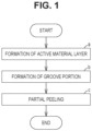
- FIG. 1 is a schematic flowchart of an electrode manufacturing method according to a present embodiment.
- the “electrode manufacturing method in the present embodiment” may be abbreviated as “the present manufacturing method”.
- the present manufacturing method includes "(a) formation of active material layer”, “(b) formation of groove portion”, and "(c) partial peeling”.
- the present manufacturing method includes forming an active material layer on a surface of an electrode current collector.
- FIG. 2 is a first schematic cross-sectional view illustrating an electrode manufacturing process.
- the electrode current collector 10 is prepared.
- the electrode current collector 10 is a sheet-shaped base material.
- the electrode current collector 10 includes a metal foil 11 and an adhesive layer 12.
- the metal foil 11 has a current collecting function.
- the metal foil 11 may have a thickness of, for example, 5 ⁇ m to 50 ⁇ m.
- the metal foil 11 may include, for example, at least one selected from the group consisting of aluminum (Al), copper (Cu), nickel (Ni), iron (Fe), chromium (Cr), and titanium (Ti).
- the metal foil 11 may include, for example, Al foil, Al alloy foil, Cu foil, Ni foil, stainless steel foil, and the like.
- FIG. 3 is a schematic plan view illustrating an example of the metal foil.
- the metal foil 11 may have, for example, a strip-shaped planar shape.
- the metal foil 11 includes a first region 11a and a second region 11b. In a longitudinal direction (Y-axis direction) of the metal foil 11, the first region 11a and the second region 11b may be alternately arranged.
- an active material layer is arranged at the electrode.
- the first region 11a can have any planar shape. In planar view, the first region 11a may have, for example, a rectangular planar shape.
- the second region 11b is an exposed region in the electrode. In the second region 11b, the metal foil 11 is exposed. The second region 11b is adjacent to the first region 11a. In planar view, the second region 11b may surround, for example, the first region 11a.
- the adhesive layer 12 covers the first region 11a (see FIG. 2 ).
- the adhesive layer 12 bonds the active material layer to the metal foil 11.
- the adhesive layer 12 may have a thickness of, for example, 0.1 ⁇ m to 5 ⁇ m.
- the adhesive layer 12 can include any adhesive.
- the adhesive layer 12 may include, for example, at least one selected from the group consisting of styrene butadiene rubber (SBR), carboxymethyl cellulose (CMC), polyacrylic acid (PAA), polyvinyl alcohol (PVA), polytetrafluoroethylene (PTFE), polyvinylidene fluoride (PVdF), and vinylidene fluoride-hexafluoropropylene copolymer (PVdF-HFP).
- the adhesive layer 12 may further include, for example, a conductive material or the like in addition to the adhesive material.
- the conductive material may include, for example, carbon black or the like.
- the adhesive layer 12 can be formed by any method.
- an adhesive composition including an adhesive may be made.
- an adhesive composition may be made by mixing a liquid material (solvent or dispersion medium) with an adhesive.
- the adhesive composition may be a solution or a particle dispersion.
- the mass fraction of the adhesive in the adhesive composition can be adjusted so that the adhesive composition exhibits the desired viscosity.
- the mass fraction of the adhesive may be, for example, 1% to 50%.
- a suitable liquid material can be selected.
- the liquid material may include, for example, at least one selected from the group consisting of water, N-methyl-2-pyrrolidone (NMP), and butyl butyrate.
- the adhesive composition may be intermittently applied to the surface of the metal foil 11 by a die coater. By drying the adhesive composition, the adhesive layer 12 can be formed. That is, the first region 11a and the second region 11b can be formed.
- the active material layer may be formed by applying a slurry to the surface of the electrode current collector 10.
- the slurry may be applied by a die coater.
- the slurry can be formed, for example, by mixing an active material, a conductive material, a binder, and a liquid material.
- the solid fraction of the slurry may be, for example, 50% to 70% or 50% to 65%.
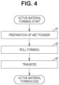
- FIG. 4 is a schematic flowchart illustrating an example of an active material layer forming method.
- “(a) formation of active material layer” may include, for example, "(a1) preparation of wet powder”, “(a2) roll forming”, and "(a3) transfer”.
- the present manufacturing method may include preparing a wet powder.
- a wet powder can be formed by mixing an active material, a binder, a conductive material, and a liquid material.
- the materials may be mixed by a stirring granulator.
- the solid fraction of the wet powder may be, for example, 70% to 99% or 75% to 90%.
- the active material may be, for example, spherical, lumpy, flake-shaped, or columnar.
- the active material can have any size.
- the active material may have, for example, a D50 of 1 ⁇ m to 30 ⁇ m or a D50 of 5 ⁇ m to 20 ⁇ m.
- the active material may be, for example, a positive electrode active material.
- the positive electrode active material can store and release lithium (Li) ions at a higher potential than that of a negative electrode active material.
- the positive electrode active material can include any component.
- the positive electrode active material may include, for example, at least one selected from the group consisting of LiCoO 2 , LiNiO 2 , LiMnO 2 , LiMn 2 O 4 , Li(NiCoMn)O 2 , Li(NiCoAl)O 2 , and LiFePO 4 .
- LiCoO 2 LiNiO 2 , LiMnO 2 , LiMn 2 O 4 , Li(NiCoMn)O 2 , Li(NiCoAl)O 2 , and LiFePO 4 .
- “(NiCoMn)" in “Li(NiCoMn)O 2 " indicates that the total composition ratio in parentheses is 1. The amount of individual components is freely selected as long as the total
- Li(NiCoMn)O 2 may include, for example, Li(Ni 1/3 Co 1/3 Mn 1/3 )O 2 , Li(Ni 0.5 Co 0.2 Mn 0.3 )O 2 , Li(Ni 0.8 Co 0.1 Mn 0.1 )O 2 .
- the negative electrode active material can store and release Li ions at a lower potential than that of the positive electrode active material.
- the negative electrode active material can include any component.
- the negative electrode active material may include, for example, at least one selected from the group consisting of graphite, soft carbon, hard carbon, silicon, silicon oxide, silicon-based alloy, tin, tin oxide, tin-based alloy, and Li 4 Ti 5 O 12 .
- the binder may be soluble or insoluble in the liquid material.
- the blending amount of the binder may be, for example, 0.1 parts by mass to 10 parts by mass with respect to 100 parts by mass of the active material.
- the binder can include any component.
- the binder may include, for example, at least one selected from the group consisting of PVdF, PTFE, PVdF-HFP, SBR, CMC, and PAA.
- the blending amount of the conductive material may be, for example, 0.1 parts by mass to 10 parts by mass with respect to 100 parts by mass of the active material.
- the conductive material can include any component.
- the conductive material may include, for example, at least one selected from the group consisting of carbon black, vapor-grown carbon fibers, carbon nanotubes, and graphene flakes.
- the carbon black may include, for example, at least one selected from the group consisting of acetylene black, furnace black, channel black, and thermal black.
- the present manufacturing method may include processing the wet powder into an active material layer by roll forming.
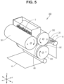
- FIG. 5 is a schematic view illustrating an example of a film forming apparatus.
- a film forming apparatus 300 can process a wet powder 2 into an active material layer 20.
- the film forming apparatus 300 includes a first roll 301, a second roll 302, and a third roll 303. Each roll rotates in the direction of the arrow. Rotation axes of the rolls are parallel to each other.
- the rotation speed of the first roll 301 is ⁇ 1
- the rotation speed of the second roll 302 is ⁇ 2
- the rotation speed of the third roll 303 is ⁇ 3, for example, the relationship of " ⁇ 1 ⁇ ⁇ 2 ⁇ ⁇ 3" may be satisfied.
- a gap AB is formed between the first roll 301 and the second roll 302.
- the wet powder 2 is supplied to the gap AB.
- the wet powder 2 is compacted and spread to form the active material layer 20 (sheet).
- the active material layer 20 may have a thickness of, for example, 10 ⁇ m to 500 ⁇ m, or may have a thickness of 50 ⁇ m to 200 ⁇ m.
- the present manufacturing method may include placing the active material layer 20 on the surface of the electrode current collector 10.
- the film forming apparatus 300 may transfer the active material layer 20 to the electrode current collector 10.
- a gap BC is formed between the second roll 302 and the third roll 303.
- the second roll 302 conveys the active material layer 20 to the gap BC.
- the third roll 303 conveys the electrode current collector 10 to the gap BC.
- the active material layer 20 is rubbed against the surface of the electrode current collector 10. As a result, the active material layer 20 adheres to the surface of the electrode current collector 10. That is, the active material layer 20 is arranged on the surface of the electrode current collector 10.
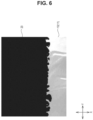
- FIG. 6 is an image illustrating an example of the end portion shape.
- FIG. 6 illustrates a portion corresponding to the region VI of FIG. 5 .
- the shape of the end portion in a width direction (X-axis direction) tends to be disordered.
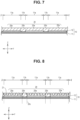
- FIG. 7 is a second schematic cross-sectional view illustrating an electrode manufacturing process.
- the active material layer 20 is formed so as to include a first portion 20a and a second portion 20b.
- the second portion 20b is adjacent to the first portion 20a.
- the first portion 20a covers the adhesive layer 12 (first region 11a).
- the second portion 20b covers the second region 11b.
- the active material layer 20 may be formed so as to cover the entire surface of the electrode current collector 10, for example.
- FIG. 8 is a third schematic cross-sectional view illustrating an electrode manufacturing process.
- the present manufacturing method includes forming a groove portion 21 on the surface of the active material layer 20.
- the groove portion 21 can be formed, for example, by embossing. That is, the groove portion 21 (recess portion) may be formed by pressing a convex shape against the surface of the active material layer 20. For example, an embossed roll may be used.
- the active material layer 20 may be dried.
- the active material layer 20 can be dried by any method. For example, a hot air drying oven may be used.
- the groove portion 21 can function as, for example, a flow path for the electrolytic solution. It is expected that the formation of the groove portion 21 will improve the battery performance (for example, cycle characteristics).
- the cross-sectional shape of the groove portion 21 is freely selected.
- the cross-sectional shape of the groove portion 21 may be rectangular, U-shaped, or V-shaped.
- the groove portion 21 may have a depth of, for example, 10 ⁇ m to 150 ⁇ m.
- the ratio of the depth of the groove portion 21 to the thickness of the active material layer 20 may be, for example, 0.1 to 0.9 or 0.3 to 0.7.
- the groove portion 21 can be formed in each of the first portion 20a and the second portion 20b. By forming the groove portion 21 in the first portion 20a, the peel strength of the first portion 20a can be improved. By forming the groove portion 21 in the second portion 20b, the peel strength of the second portion 20b can be reduced.
- a part of the groove portion 21 may be formed along a boundary 20c between the first portion 20a and the second portion 20b.
- the portion of the groove portion 21 along the boundary 20c can function as a cut line of the active material layer 20.
- the boundary 20c can be located directly above a boundary between the first region 11a and the second region 11b.
- a part of the groove portion 21 may extend linearly along the boundary 20c.
- a part of the groove portion 21 may substantially coincide with the position of the boundary 20c.
- a part of the groove portion 21 can function as a cut line even when it is slightly separated from the boundary 20c.
- the distance between a part of the groove portion 21 and the boundary 20c may be, for example, 0 mm to 10 mm.
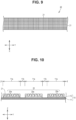
- FIG. 9 is a schematic plan view illustrating an example of the groove portion.
- the groove portion 21 can have any planar pattern.
- the groove portion 21 may be formed in a numerously-lined shape, for example.
- the groove portion 21 may be formed in a grid pattern shape, for example.
- the pitch (interval between adjacent parallel lines) of the groove portion 21 may be, for example, 0.1 mm to 10 mm or 0.5 mm to 5 mm.
- FIG. 10 is a fourth schematic cross-sectional view illustrating an electrode manufacturing process.
- the present manufacturing method includes peeling a part of the active material layer 20. That is, the second portion 20b is peeled off. Since the peel strength of the second portion 20b is low, the second portion 20b can be peeled by a weak stimulus. For example, vibration may be applied to the second portion 20b. For example, the second portion 20b may be sucked by a suction pump. The peeled second portion 20b may be reused as a raw material for the wet powder, for example.
- FIG. 11 is a schematic plan view illustrating an example of the electrodes in the present embodiment.
- the “electrode in the present embodiment” may be abbreviated as the “present electrode”.
- the present electrode 100 can be manufactured by peeling off the second portion 20b.
- the present electrode 100 includes the active material layer 20.
- the active material layer 20 corresponds to the first portion 20a.
- the active material layer 20 can have a planar shape corresponding to the first region 11a (adhesive layer 12).
- FIG. 12 is an image illustrating an actual partial peeling.
- the second portion 20b can be peeled off so as to be cut off. After the peeling of the second portion 20b, the disorder of the end portion shape of the first portion 20a is small.
- the first portion 20a can have a rectangular planar shape. The periphery of the first portion 20a can be straight.
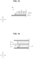
- FIG. 13 is a schematic cross-sectional view illustrating the electrodes in the present embodiment.
- the present electrode 100 includes the electrode current collector 10 and the active material layer 20.
- the active material layer 20 may be arranged on only one side of the electrode current collector 10, or may be arranged on both the front and back sides thereof.
- the active material layer 20 in FIG. 13 corresponds to the first portion 20a in FIG. 7 and the like.
- the active material layer 20 covers the adhesive layer 12.
- the region where the metal foil 11 is exposed corresponds to the second region 11b in FIG. 3 and the like.
- the groove portion 21 is formed on the surface of the active material layer 20.
- the disorder of the end portion shape of the present electrode 100 is small.
- the active material layer 20 can have a steep end surface.
- the end surface of the active material layer 20 can have an inclination angle ⁇ of 45 degrees or more.
- the inclination angle ⁇ may be, for example, 60 degrees to 90 degrees or 75 degrees to 90 degrees. It is expected that the energy density improves as the inclination angle ⁇ approaches 90 degrees.
- FIG. 14 is a first conceptual diagram illustrating the relationship between the inclination angle of the end surface and the energy density.
- the present electrode 100 faces a counter electrode 200 with a separator 400 interposed therebetween.
- the counter electrode 200 has the opposite polarity to the present electrode 100.
- the present electrode 100 is a positive electrode
- the counter electrode 200 is a negative electrode.
- a dead space 20s may be formed at the end portion of the present electrode 100 at a portion facing the counter electrode 200. The formation of the dead space 20s can reduce the energy density.
- FIG. 15 is a second conceptual diagram illustrating the relationship between the inclination angle of the end surface and the energy density.
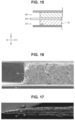
- FIG. 16 is an image indicating an application example of the present embodiment.
- FIG. 16 illustrates a cross-sectional SEM image of the electrode.
- the active material layer 20 in FIG. 16 is formed of a wet powder.
- the end surface of the active material layer 20 is formed by partial peeling of the present embodiment.
- the active material layer 20 has a steep end surface. The inclination angle of the end surface is 45 degrees or more.
- FIG. 17 is an image illustrating a reference form.
- FIG. 17 illustrates a cross-sectional SEM image of the electrode.
- the active material layer 20 in FIG. 17 is formed of a slurry.
- the partial peeling of the present embodiment has not been carried out. Since the slurry has high fluidity, dripping tends to occur at the end portion of the coating film. The dripping can reduce the inclination angle of the end surface. The inclination angle of the end surface is less than 45 degrees.
- the present embodiment is exemplary in all respects.
- the present embodiment is not restrictive.
- the technical scope of the present disclosure includes the meaning equivalent to the description of the scope of claims and all modifications within the scope thereof. For example, it is planned from the beginning that any configurations may be extracted from the present embodiment and appropriately combined.
Landscapes
- Chemical & Material Sciences (AREA)
- Engineering & Computer Science (AREA)
- Chemical Kinetics & Catalysis (AREA)
- Electrochemistry (AREA)
- General Chemical & Material Sciences (AREA)
- Materials Engineering (AREA)
- Manufacturing & Machinery (AREA)
- Composite Materials (AREA)
- Battery Electrode And Active Subsutance (AREA)
- Cell Electrode Carriers And Collectors (AREA)
- Electric Double-Layer Capacitors Or The Like (AREA)
Abstract
Description
- The present disclosure relates to an electrode manufacturing method, an electrode current collector, and an electrode.
-
Japanese Unexamined Patent Application Publication No. 2013-017962 - An electrode can be manufactured by forming an active material layer on a surface of an electrode current collector. The active material layer may be formed intermittently. The surface of the electrode current collector is exposed in a portion where the active material layer is not formed. Hereinafter, a portion where the surface of the electrode current collector is exposed is also referred to as an "exposed region". The exposed region can function as a reserve space for cutting of the electrode, a welded portion of a current collecting member, and the like.
- Due to the intermittent formation of the active material layer, the shape of the end portion (periphery) of the active material layer may be disordered. The disordered end portion shape can, for example, reduce battery performance.
- The present disclosure provides an electrode manufacturing method capable of intermittently forming an active material layer.
- Hereinafter, technical configurations and action effects of the present disclosure will be described. However, the action mechanism of the present specification includes estimation. The action mechanism does not limit the technical scope of the present disclosure.
- An electrode manufacturing method according to a first aspect of the present disclosure includes manufacturing an electrode by forming an active material layer on a surface of an electrode current collector, forming a groove portion on a surface of the active material layer, and peeling off a part of the active material layer. In planar view, the electrode current collector includes a metal foil and an adhesive layer. The metal foil includes a first region and a second region. The adhesive layer covers the first region. The second region is adjacent to the first region. In the second region, the metal foil is exposed. The active material layer is formed to include a first portion and a second portion. The second portion is adjacent to the first portion. The first portion covers the adhesive layer. The second portion covers the second region. The groove portion is formed in each of the first portion and the second portion. As the part of the active material layer, the second portion is peeled off.
- The electrode current collector includes the first region and the second region. The first region is the region where the active material layer is arranged in the electrode. The second region is an exposed region in the electrode. The first region is covered with the adhesive layer.
- The active material layer includes the first portion and the second portion. The first portion is formed on the first region (adhesive layer). The second portion is formed on the second region (metal foil). The groove portion is formed in the active material layer. The groove portion is formed in each of the first portion and the second portion. The adhesive layer is between the first portion and the metal foil. Due to the formation of the groove portion, the first portion is firmly adhered to the metal foil. That is, the peel strength of the first portion can be improved. On the other hand, there is no adhesive layer between the second portion and the metal foil. The formation of the groove portion makes the second portion weak, so the peel strength of the second portion may rather decrease.
- Due to the difference in peel strength between the first portion and the second portion, the second portion can be easily peeled. By peeling off the second portion, the first portion (active material layer) with a less disordered end portion shape remains according to the planar shape of the first region (adhesive layer). That is, the active material layers can be formed intermittently.
- In the first aspect, the forming of the active material layer may include preparing a wet powder, processing the wet powder into the active material layer by roll forming, and arranging the active material layer on the surface of the electrode current collector.
- In the configuration, the active material layer can be formed by any method. For example, the active material layer may be formed by applying a slurry.
- For example, the active material layer may be formed by roll forming of a wet powder. The wet powder is an aggregate of grains. In roll forming, a sheet (active material layer) is formed by spreading the aggregate of grains, so that the shape of the end portion tends to be disordered. In the manufacturing method, even when the work is a wet powder, the disorder of the end portion shape can be reduced.
- In the first aspect, a part of the groove portion may be formed along a boundary between the first portion and the second portion.
- The groove portion along the boundary between the first portion and the second portion can act like a cut line (perforation) when the second portion is peeled off. It is expected that the disorder of the end portion shape will be further reduced in the first portion (final active material layer) by having a part of the groove portion function as a cut line.
- In the first aspect, the part of the active material layer may be peeled by applying vibration to the second portion.
- The second portion is expected to be peeled by a weak stimulus. For example, vibration may be applied to the second portion.
- An electrode current collector according to a second aspect of the present disclosure includes a metal foil and an adhesive layer. In planar view, the metal foil includes a first region and a second region. The adhesive layer covers the first region. The second region is adjacent to the first region. In the second region, the metal foil is exposed.
- The electrode current collector is suitable as the electrode current collector according to the first aspect.
- In the second aspect, in the planar view, the metal foil may have a strip-shaped planar shape. In a longitudinal direction of the metal foil, the first region and the second region may be alternately arranged.
- In the second aspect, in the planar view, the first region may have a rectangular planar shape.
- In the second aspect, in the planar view, the second region may surround the first region.
- An electrode according to a third aspect of the present disclosure includes the electrode current collector and an active material layer. The active material layer covers the adhesive layer. A groove portion is formed on a surface of the active material layer. An end surface of the active material layer has an inclination angle of 45 degrees or more.
- In the electrode manufactured by the manufacturing method, the shape of the end portion of the active material layer (first portion) is less disordered. The active material layer can have, for example, a steep end surface. That is, the end surface of the active material layer can have an inclination angle of 45 degrees or more. The steep end surface of the active material layer is expected to improve the energy density, for example.
- Hereinafter, an embodiment of the present disclosure (which hereinafter may be abbreviated as "the present embodiment") will be described. However, the present embodiment does not limit the technical scope of the present disclosure.
- Features, advantages, and technical and industrial significance of exemplary embodiments of the invention will be described below with reference to the accompanying drawings, in which like signs denote like elements, and wherein:
-
FIG. 1 is a schematic flowchart of an electrode manufacturing method according to an embodiment; -
FIG. 2 is a first schematic cross-sectional diagram illustrating an electrode manufacturing process; -
FIG. 3 is a schematic plan view illustrating an example of a metal foil; -
FIG. 4 is a schematic flowchart illustrating an example of an active material layer forming method; -
FIG. 5 is a schematic view illustrating an example of a film forming apparatus; -
FIG. 6 is an image illustrating an example of an end portion shape; -
FIG. 7 is a second schematic cross-sectional diagram illustrating an electrode manufacturing process; -
FIG. 8 is a third schematic cross-sectional diagram illustrating an electrode manufacturing process; -
FIG. 9 is a schematic plan view illustrating an example of a groove portion; -
FIG. 10 is a fourth schematic cross-sectional diagram illustrating an electrode manufacturing process; -
FIG. 11 is a schematic plan view illustrating an example of an electrode in the present embodiment; -
FIG. 12 is an image illustrating an actual partial peeling; -
FIG. 13 is a schematic cross-sectional diagram illustrating an electrode in the present embodiment; -
FIG. 14 is a first conceptual diagram illustrating a relationship between an inclination angle of an end surface and an energy density; -
FIG. 15 is a second conceptual diagram illustrating a relationship between an inclination angle of an end surface and an energy density; -
FIG. 16 is an image illustrating an application example of the present embodiment; and -
FIG. 17 is an image illustrating a reference form. - In the present specification, the description of "including", "containing", "having", and variations thereof (for example, "constituted of") is in an open-ended format. The open-ended format may or may not include additional elements in addition to the required elements. The description "consisting of" is in a closed format. However, even in the closed format, additional elements that are normally associated impurities or that are irrelevant to the disclosed art are not excluded. The description of "substantially consists of..." is in a semi-closed format. In the semi-closed format, the addition of elements that do not substantially affect the basic and novel properties of the disclosed art is permissible.
- In the present specification, expressions such as "may" and "can" are used in the permissive meaning of "there is a possibility" rather than the obligatory meaning of "it must be done".
- In the present specification, the execution order of a plurality of steps, movements, operations, and the like included in various methods is not limited to the description order, unless otherwise specified. For example, a plurality of steps may proceed simultaneously. For example, a plurality of steps may be in phase with each other.
- In the present specification, a numerical range such as "m% to n%" includes an upper limit value and a lower limit value, unless otherwise specified. That is, "m% to n%" indicates a numerical range of "m% or more and n% or less". Further, "m% or more and n% or less" includes "more than m% and less than n%". Further, a numerical value randomly selected from the numerical range may be set as a new upper limit value or a lower limit value. For example, a new numerical range may be set by appropriately combining a numerical value within the numerical range with a numerical value described in another part in the present specification, in a table, in a figure, or the like.
- In the present specification, all numerical values are modified by the term "about". The term "about" can mean, for example, ±5%, ±3%, ±1%, and the like. All numerical values can be approximate values that can change depending on the usage pattern of the disclosed art. All numbers may be displayed in significant figures. The measured value can be an average value in multiple measurements. The number of measurements may be three or more, five or more, or ten or more. Generally, it is expected that the reliability of the average value improves as the number of measurements increases. The measured value may be rounded off based on the number of significant digits. The measured value may include, for example, an error due to a detection limit of a measuring device.
- Geometric terms (for example, "parallel", "vertical", and "orthogonal") in the present specification should not be understood in a strict sense. For example, "parallel" may deviate slightly from "parallel" in the strict sense. Geometric terms in the present specification can include, for example, tolerances or errors in design, work, and manufacturing. The dimensional relationships in each drawing may not match the actual dimensional relationships. In order to help the understanding of the disclosed art, the dimensional relations (length, width, thickness, and the like) in each drawing may be changed. Furthermore, some configurations may be omitted.
- As used in the present specification, "planar view" indicates that a target object is viewed with a line of sight parallel to a thickness direction of the target object. The planar view is drawn on the plan view. As used in the present specification, "cross-sectional view" indicates that a target object is viewed with a line of sight orthogonal to the thickness direction of the target object. The cross-sectional view is drawn in the cross-sectional diagram.
- As used in the present specification, the "inclination angle" indicates the angle (acute angle and right angle) formed by an end surface of an active material layer and a surface of an electrode current collector in a cross-sectional view.
- In the present specification, when a compound is represented by a stoichiometric composition formula (for example, "LiCoO2"), the stoichiometric composition formula is only a representative example of the compound. The compound may have a non-stoichiometric composition. For example, when lithium cobalt oxide is described as "LiCoO2", unless otherwise specified, lithium cobalt oxide is not limited to the composition ratio of "Li / Co / O = 1 / 1 / 2" and can include Li, Co, and O in any composition ratio. Furthermore, doping, substitution, and the like with trace elements can be allowed.
- As used in the present specification, the term "electrode" is a general term for a positive electrode and a negative electrode. The electrode may be a positive electrode or a negative electrode. The electrode can be applied to any battery system. The electrode may be, for example, for a lithium ion battery.
- As used in the present specification, the term "solid fraction" indicates the total mass fraction (percentage) of components other than the liquid material in a solid-liquid mixture. The solid fraction can also be referred to as "nonvolatile content (NV)". A component (solute) dissolved in a liquid material is considered to be a component other than the liquid material.
- As used in the present specification, the term "slurry" refers to a dispersion system in which a solid material (powder) is dispersed in a liquid material. The term "wet powder" indicates a dispersion system in which a liquid material is dispersed in a solid material (powder).
- As used in the present specification, "D50" is defined as a particle size in which the cumulative frequency from the smaller particle size reaches 50% in the volume-based particle size distribution. The volume-based particle size distribution can be measured by a laser diffraction type particle size distribution measuring device.
-
FIG. 1 is a schematic flowchart of an electrode manufacturing method according to a present embodiment. Hereinafter, the "electrode manufacturing method in the present embodiment" may be abbreviated as "the present manufacturing method". The present manufacturing method includes "(a) formation of active material layer", "(b) formation of groove portion", and "(c) partial peeling". - The present manufacturing method includes forming an active material layer on a surface of an electrode current collector.
-
FIG. 2 is a first schematic cross-sectional view illustrating an electrode manufacturing process. The electrodecurrent collector 10 is prepared. The electrodecurrent collector 10 is a sheet-shaped base material. The electrodecurrent collector 10 includes ametal foil 11 and anadhesive layer 12. - The
metal foil 11 has a current collecting function. Themetal foil 11 may have a thickness of, for example, 5 µm to 50 µm. Themetal foil 11 may include, for example, at least one selected from the group consisting of aluminum (Al), copper (Cu), nickel (Ni), iron (Fe), chromium (Cr), and titanium (Ti). Themetal foil 11 may include, for example, Al foil, Al alloy foil, Cu foil, Ni foil, stainless steel foil, and the like. -
FIG. 3 is a schematic plan view illustrating an example of the metal foil. In a planar view, themetal foil 11 may have, for example, a strip-shaped planar shape. Themetal foil 11 includes afirst region 11a and asecond region 11b. In a longitudinal direction (Y-axis direction) of themetal foil 11, thefirst region 11a and thesecond region 11b may be alternately arranged. - In the
first region 11a, an active material layer is arranged at the electrode. Thefirst region 11a can have any planar shape. In planar view, thefirst region 11a may have, for example, a rectangular planar shape. - The
second region 11b is an exposed region in the electrode. In thesecond region 11b, themetal foil 11 is exposed. Thesecond region 11b is adjacent to thefirst region 11a. In planar view, thesecond region 11b may surround, for example, thefirst region 11a. - The
adhesive layer 12 covers thefirst region 11a (seeFIG. 2 ). Theadhesive layer 12 bonds the active material layer to themetal foil 11. Theadhesive layer 12 may have a thickness of, for example, 0.1 µm to 5 µm. Theadhesive layer 12 can include any adhesive. Theadhesive layer 12 may include, for example, at least one selected from the group consisting of styrene butadiene rubber (SBR), carboxymethyl cellulose (CMC), polyacrylic acid (PAA), polyvinyl alcohol (PVA), polytetrafluoroethylene (PTFE), polyvinylidene fluoride (PVdF), and vinylidene fluoride-hexafluoropropylene copolymer (PVdF-HFP). Theadhesive layer 12 may further include, for example, a conductive material or the like in addition to the adhesive material. The conductive material may include, for example, carbon black or the like. - The
adhesive layer 12 can be formed by any method. For example, an adhesive composition including an adhesive may be made. For example, an adhesive composition may be made by mixing a liquid material (solvent or dispersion medium) with an adhesive. The adhesive composition may be a solution or a particle dispersion. The mass fraction of the adhesive in the adhesive composition can be adjusted so that the adhesive composition exhibits the desired viscosity. The mass fraction of the adhesive may be, for example, 1% to 50%. Depending on the type of adhesive, a suitable liquid material can be selected. The liquid material may include, for example, at least one selected from the group consisting of water, N-methyl-2-pyrrolidone (NMP), and butyl butyrate. - For example, the adhesive composition may be intermittently applied to the surface of the
metal foil 11 by a die coater. By drying the adhesive composition, theadhesive layer 12 can be formed. That is, thefirst region 11a and thesecond region 11b can be formed. - For example, the active material layer may be formed by applying a slurry to the surface of the electrode
current collector 10. For example, the slurry may be applied by a die coater. The slurry can be formed, for example, by mixing an active material, a conductive material, a binder, and a liquid material. The solid fraction of the slurry may be, for example, 50% to 70% or 50% to 65%. -
FIG. 4 is a schematic flowchart illustrating an example of an active material layer forming method. "(a) formation of active material layer" may include, for example, "(a1) preparation of wet powder", "(a2) roll forming", and "(a3) transfer". - The present manufacturing method may include preparing a wet powder. For example, a wet powder can be formed by mixing an active material, a binder, a conductive material, and a liquid material. For example, the materials may be mixed by a stirring granulator. The solid fraction of the wet powder may be, for example, 70% to 99% or 75% to 90%.
- The active material may be, for example, spherical, lumpy, flake-shaped, or columnar. The active material can have any size. The active material may have, for example, a D50 of 1 µm to 30 µm or a D50 of 5 µm to 20 µm.
- The active material may be, for example, a positive electrode active material. The positive electrode active material can store and release lithium (Li) ions at a higher potential than that of a negative electrode active material. The positive electrode active material can include any component. The positive electrode active material may include, for example, at least one selected from the group consisting of LiCoO2, LiNiO2, LiMnO2, LiMn2O4, Li(NiCoMn)O2, Li(NiCoAl)O2, and LiFePO4. For example, "(NiCoMn)" in "Li(NiCoMn)O2" indicates that the total composition ratio in parentheses is 1. The amount of individual components is freely selected as long as the total is 1. Li(NiCoMn)O2 may include, for example, Li(Ni1/3Co1/3Mn1/3)O2, Li(Ni0.5Co0.2Mn0.3)O2, Li(Ni0.8Co0.1Mn0.1)O2.
- The negative electrode active material can store and release Li ions at a lower potential than that of the positive electrode active material. The negative electrode active material can include any component. The negative electrode active material may include, for example, at least one selected from the group consisting of graphite, soft carbon, hard carbon, silicon, silicon oxide, silicon-based alloy, tin, tin oxide, tin-based alloy, and Li4Ti5O12.
- The binder may be soluble or insoluble in the liquid material. The blending amount of the binder may be, for example, 0.1 parts by mass to 10 parts by mass with respect to 100 parts by mass of the active material. The binder can include any component. The binder may include, for example, at least one selected from the group consisting of PVdF, PTFE, PVdF-HFP, SBR, CMC, and PAA.
- The blending amount of the conductive material may be, for example, 0.1 parts by mass to 10 parts by mass with respect to 100 parts by mass of the active material. The conductive material can include any component. The conductive material may include, for example, at least one selected from the group consisting of carbon black, vapor-grown carbon fibers, carbon nanotubes, and graphene flakes. The carbon black may include, for example, at least one selected from the group consisting of acetylene black, furnace black, channel black, and thermal black.
- The present manufacturing method may include processing the wet powder into an active material layer by roll forming.
-
FIG. 5 is a schematic view illustrating an example of a film forming apparatus. Afilm forming apparatus 300 can process awet powder 2 into anactive material layer 20. Thefilm forming apparatus 300 includes afirst roll 301, asecond roll 302, and athird roll 303. Each roll rotates in the direction of the arrow. Rotation axes of the rolls are parallel to each other. When the rotation speed of thefirst roll 301 is ω 1, the rotation speed of thesecond roll 302 is ω2, and the rotation speed of thethird roll 303 is ω3, for example, the relationship of "ω1 < ω2 < ω3" may be satisfied. - A gap AB is formed between the
first roll 301 and thesecond roll 302. Thewet powder 2 is supplied to the gap AB. In the gap AB, thewet powder 2 is compacted and spread to form the active material layer 20 (sheet). Theactive material layer 20 may have a thickness of, for example, 10 µm to 500 µm, or may have a thickness of 50 µm to 200 µm. - The present manufacturing method may include placing the
active material layer 20 on the surface of the electrodecurrent collector 10. For example, thefilm forming apparatus 300 may transfer theactive material layer 20 to the electrodecurrent collector 10. A gap BC is formed between thesecond roll 302 and thethird roll 303. Thesecond roll 302 conveys theactive material layer 20 to the gap BC. Thethird roll 303 conveys the electrodecurrent collector 10 to the gap BC. - In the gap BC, the
active material layer 20 is rubbed against the surface of the electrodecurrent collector 10. As a result, theactive material layer 20 adheres to the surface of the electrodecurrent collector 10. That is, theactive material layer 20 is arranged on the surface of the electrodecurrent collector 10. -
FIG. 6 is an image illustrating an example of the end portion shape.FIG. 6 illustrates a portion corresponding to the region VI ofFIG. 5 . In the method of forming theactive material layer 20 with the wet powder, the shape of the end portion in a width direction (X-axis direction) tends to be disordered. -
FIG. 7 is a second schematic cross-sectional view illustrating an electrode manufacturing process. Theactive material layer 20 is formed so as to include afirst portion 20a and asecond portion 20b. Thesecond portion 20b is adjacent to thefirst portion 20a. Thefirst portion 20a covers the adhesive layer 12 (first region 11a). Thesecond portion 20b covers thesecond region 11b. Theactive material layer 20 may be formed so as to cover the entire surface of the electrodecurrent collector 10, for example. -
FIG. 8 is a third schematic cross-sectional view illustrating an electrode manufacturing process. The present manufacturing method includes forming agroove portion 21 on the surface of theactive material layer 20. Thegroove portion 21 can be formed, for example, by embossing. That is, the groove portion 21 (recess portion) may be formed by pressing a convex shape against the surface of theactive material layer 20. For example, an embossed roll may be used. - After forming the
groove portion 21, theactive material layer 20 may be dried. Theactive material layer 20 can be dried by any method. For example, a hot air drying oven may be used. - The
groove portion 21 can function as, for example, a flow path for the electrolytic solution. It is expected that the formation of thegroove portion 21 will improve the battery performance (for example, cycle characteristics). The cross-sectional shape of thegroove portion 21 is freely selected. The cross-sectional shape of thegroove portion 21 may be rectangular, U-shaped, or V-shaped. Thegroove portion 21 may have a depth of, for example, 10 µm to 150 µm. The ratio of the depth of thegroove portion 21 to the thickness of theactive material layer 20 may be, for example, 0.1 to 0.9 or 0.3 to 0.7. - The
groove portion 21 can be formed in each of thefirst portion 20a and thesecond portion 20b. By forming thegroove portion 21 in thefirst portion 20a, the peel strength of thefirst portion 20a can be improved. By forming thegroove portion 21 in thesecond portion 20b, the peel strength of thesecond portion 20b can be reduced. - A part of the
groove portion 21 may be formed along aboundary 20c between thefirst portion 20a and thesecond portion 20b. The portion of thegroove portion 21 along theboundary 20c can function as a cut line of theactive material layer 20. Theboundary 20c can be located directly above a boundary between thefirst region 11a and thesecond region 11b. A part of thegroove portion 21 may extend linearly along theboundary 20c. A part of thegroove portion 21 may substantially coincide with the position of theboundary 20c. A part of thegroove portion 21 can function as a cut line even when it is slightly separated from theboundary 20c. The distance between a part of thegroove portion 21 and theboundary 20c may be, for example, 0 mm to 10 mm. -
FIG. 9 is a schematic plan view illustrating an example of the groove portion. Thegroove portion 21 can have any planar pattern. Thegroove portion 21 may be formed in a numerously-lined shape, for example. Thegroove portion 21 may be formed in a grid pattern shape, for example. The pitch (interval between adjacent parallel lines) of thegroove portion 21 may be, for example, 0.1 mm to 10 mm or 0.5 mm to 5 mm. -
FIG. 10 is a fourth schematic cross-sectional view illustrating an electrode manufacturing process. The present manufacturing method includes peeling a part of theactive material layer 20. That is, thesecond portion 20b is peeled off. Since the peel strength of thesecond portion 20b is low, thesecond portion 20b can be peeled by a weak stimulus. For example, vibration may be applied to thesecond portion 20b. For example, thesecond portion 20b may be sucked by a suction pump. The peeledsecond portion 20b may be reused as a raw material for the wet powder, for example. -
FIG. 11 is a schematic plan view illustrating an example of the electrodes in the present embodiment. Hereinafter, the "electrode in the present embodiment" may be abbreviated as the "present electrode". Thepresent electrode 100 can be manufactured by peeling off thesecond portion 20b. Thepresent electrode 100 includes theactive material layer 20. Theactive material layer 20 corresponds to thefirst portion 20a. Theactive material layer 20 can have a planar shape corresponding to thefirst region 11a (adhesive layer 12). -
FIG. 12 is an image illustrating an actual partial peeling. Thesecond portion 20b can be peeled off so as to be cut off. After the peeling of thesecond portion 20b, the disorder of the end portion shape of thefirst portion 20a is small. Thefirst portion 20a can have a rectangular planar shape. The periphery of thefirst portion 20a can be straight. -
FIG. 13 is a schematic cross-sectional view illustrating the electrodes in the present embodiment. Thepresent electrode 100 includes the electrodecurrent collector 10 and theactive material layer 20. Theactive material layer 20 may be arranged on only one side of the electrodecurrent collector 10, or may be arranged on both the front and back sides thereof. Theactive material layer 20 inFIG. 13 corresponds to thefirst portion 20a inFIG. 7 and the like. Theactive material layer 20 covers theadhesive layer 12. The region where themetal foil 11 is exposed corresponds to thesecond region 11b inFIG. 3 and the like. Thegroove portion 21 is formed on the surface of theactive material layer 20. - The disorder of the end portion shape of the
present electrode 100 is small. In thepresent electrode 100, theactive material layer 20 can have a steep end surface. The end surface of theactive material layer 20 can have an inclination angle θ of 45 degrees or more. The inclination angle θ may be, for example, 60 degrees to 90 degrees or 75 degrees to 90 degrees. It is expected that the energy density improves as the inclination angle θ approaches 90 degrees. -
FIG. 14 is a first conceptual diagram illustrating the relationship between the inclination angle of the end surface and the energy density. InFIGS. 14 and15 , the groove portion and the adhesive layer are omitted for convenience. Thepresent electrode 100 faces acounter electrode 200 with aseparator 400 interposed therebetween. Thecounter electrode 200 has the opposite polarity to thepresent electrode 100. For example, when thepresent electrode 100 is a positive electrode, thecounter electrode 200 is a negative electrode. When the inclination angle θ of the end surface is small, adead space 20s may be formed at the end portion of thepresent electrode 100 at a portion facing thecounter electrode 200. The formation of thedead space 20s can reduce the energy density. -
FIG. 15 is a second conceptual diagram illustrating the relationship between the inclination angle of the end surface and the energy density. The closer the inclination angle θ is to 90 degrees, the smaller thedead space 20s can be. That is, it is expected that the energy density improves as the inclination angle θ approaches 90 degrees. -
FIG. 16 is an image indicating an application example of the present embodiment.FIG. 16 illustrates a cross-sectional SEM image of the electrode. Theactive material layer 20 inFIG. 16 is formed of a wet powder. The end surface of theactive material layer 20 is formed by partial peeling of the present embodiment. Theactive material layer 20 has a steep end surface. The inclination angle of the end surface is 45 degrees or more. -
FIG. 17 is an image illustrating a reference form.FIG. 17 illustrates a cross-sectional SEM image of the electrode. Theactive material layer 20 inFIG. 17 is formed of a slurry. In the reference form, the partial peeling of the present embodiment has not been carried out. Since the slurry has high fluidity, dripping tends to occur at the end portion of the coating film. The dripping can reduce the inclination angle of the end surface. The inclination angle of the end surface is less than 45 degrees. - The present embodiment is exemplary in all respects. The present embodiment is not restrictive. The technical scope of the present disclosure includes the meaning equivalent to the description of the scope of claims and all modifications within the scope thereof. For example, it is planned from the beginning that any configurations may be extracted from the present embodiment and appropriately combined.
Claims (9)
- An electrode manufacturing method comprising:
manufacturing an electrode (100) by:forming an active material layer (20) on a surface of an electrode current collector (10);forming a groove portion (21) on a surface of the active material layer (20); andpeeling off a part of the active material layer (20), wherein:the electrode current collector (10) includes a metal foil (11) and an adhesive layer (12);in planar view, the metal foil (11) includes a first region (11a) and a second region (11b);the adhesive layer (12) covers the first region (11a);the second region (11b) is adjacent to the first region (11a);in the second region (11b), the metal foil (11) is exposed;the active material layer (20) is formed to include a first portion (20a) and a second portion (20b);the second portion (20b) is adjacent to the first portion (20a);the first portion (20a) covers the adhesive layer (12);the second portion (20b) covers the second region (11b);the groove portion (21) is formed in each of the first portion (20a) and the second portion (20b); andas the part of the active material layer (20), the second portion (20b) is peeled off. - The electrode manufacturing method according to claim 1, wherein the forming of the active material layer (20) includes:preparing a wet powder (2);processing the wet powder (2) into the active material layer (20) by roll forming; andarranging the active material layer (20) on the surface of the electrode current collector (10).
- The electrode manufacturing method according to claim 1 or 2, wherein a part of the groove portion (21) is formed along a boundary between the first portion (20a) and the second portion (20b).
- The electrode manufacturing method according to any one of claims 1 to 3, wherein the part of the active material layer (20) is peeled by applying vibration to the second portion (20b).
- An electrode current collector (10) comprising:a metal foil (11); andan adhesive layer (12), wherein:in planar view, the metal foil (11) includes a first region (11a) and a second region (11b);the adhesive layer (12) covers the first region (11a);the second region (11b) is adjacent to the first region (11a); andin the second region (11b), the metal foil (11) is exposed.
- The electrode current collector (10) according to claim 5, wherein:in the planar view, the metal foil (11) has a strip-shaped planar shape; andin a longitudinal direction of the metal foil (11), the first region (11a) and the second region (11b) are alternately arranged.
- The electrode current collector (10) according to claim 5 or 6, wherein, in the planar view, the first region (11a) has a rectangular planar shape.
- The electrode current collector (10) according to any one of claims 5 to 7, wherein, in the planar view, the second region (11b) surrounds the first region (11a).
- An electrode comprising:the electrode current collector (10) according to any one of claims 5 to 8; andan active material layer (20), wherein:the active material layer (20) covers a adhesive layer (12);a groove portion (21) is formed on a surface of the active material layer (20); andan end surface of the active material layer (20) has an inclination angle of 45 degrees or more.
Applications Claiming Priority (1)
| Application Number | Priority Date | Filing Date | Title |
|---|---|---|---|
| JP2022002209A JP7794642B2 (en) | 2022-01-11 | 2022-01-11 | Electrode manufacturing method |
Publications (2)
| Publication Number | Publication Date |
|---|---|
| EP4210125A2 true EP4210125A2 (en) | 2023-07-12 |
| EP4210125A3 EP4210125A3 (en) | 2023-08-02 |
Family
ID=84329856
Family Applications (1)
| Application Number | Title | Priority Date | Filing Date |
|---|---|---|---|
| EP22205135.1A Pending EP4210125A3 (en) | 2022-01-11 | 2022-11-02 | Electrode manufacturing method, electrode current collector, and electrode |
Country Status (5)
| Country | Link |
|---|---|
| US (1) | US12592391B2 (en) |
| EP (1) | EP4210125A3 (en) |
| JP (1) | JP7794642B2 (en) |
| KR (1) | KR20230108693A (en) |
| CN (1) | CN116470007B (en) |
Citations (1)
| Publication number | Priority date | Publication date | Assignee | Title |
|---|---|---|---|---|
| JP2013017962A (en) | 2011-07-12 | 2013-01-31 | Panasonic Corp | Coating apparatus |
Family Cites Families (11)
| Publication number | Priority date | Publication date | Assignee | Title |
|---|---|---|---|---|
| JPH05283831A (en) * | 1992-03-31 | 1993-10-29 | Nippon Rika Kogyosho:Kk | Copper-clad laminate |
| DE69830712T2 (en) * | 1997-04-23 | 2005-12-15 | Japan Storage Battery Co. Ltd., Kyoto | ELECTRODE AND BATTERY |
| JP4619465B2 (en) * | 1998-07-13 | 2011-01-26 | 大日本印刷株式会社 | Method for producing electrode plate for non-aqueous electrolyte secondary battery |
| JP2004273181A (en) * | 2003-03-06 | 2004-09-30 | Dainippon Printing Co Ltd | Electrode plate for battery |
| JP4672079B2 (en) * | 2009-01-14 | 2011-04-20 | パナソニック株式会社 | Non-aqueous battery negative electrode plate, non-aqueous battery electrode group and manufacturing method thereof, cylindrical non-aqueous secondary battery and manufacturing method thereof |
| JP5539150B2 (en) * | 2010-10-25 | 2014-07-02 | 矢崎総業株式会社 | Wiring board manufacturing method |
| WO2014192631A1 (en) * | 2013-05-31 | 2014-12-04 | 三井化学東セロ株式会社 | Electronic member peeling method and laminated body |
| JP2017157495A (en) | 2016-03-04 | 2017-09-07 | トヨタ自動車株式会社 | Electrode sheet manufacturing method |
| TWI685996B (en) * | 2018-06-13 | 2020-02-21 | 金碳洁股份有限公司 | Rechargeable battery and electrode thereof |
| JP7205426B2 (en) | 2019-09-09 | 2023-01-17 | トヨタ自動車株式会社 | Electrode sheet manufacturing method |
| JP2022093073A (en) * | 2020-12-11 | 2022-06-23 | 株式会社豊田自動織機 | Manufacturing method of electrode sheet |
-
2022
- 2022-01-11 JP JP2022002209A patent/JP7794642B2/en active Active
- 2022-10-27 KR KR1020220140721A patent/KR20230108693A/en active Pending
- 2022-11-02 EP EP22205135.1A patent/EP4210125A3/en active Pending
- 2022-11-03 CN CN202211369461.7A patent/CN116470007B/en active Active
- 2022-11-04 US US17/981,184 patent/US12592391B2/en active Active
Patent Citations (1)
| Publication number | Priority date | Publication date | Assignee | Title |
|---|---|---|---|---|
| JP2013017962A (en) | 2011-07-12 | 2013-01-31 | Panasonic Corp | Coating apparatus |
Also Published As
| Publication number | Publication date |
|---|---|
| US12592391B2 (en) | 2026-03-31 |
| KR20230108693A (en) | 2023-07-18 |
| CN116470007A (en) | 2023-07-21 |
| CN116470007B (en) | 2026-01-30 |
| US20230223549A1 (en) | 2023-07-13 |
| EP4210125A3 (en) | 2023-08-02 |
| JP7794642B2 (en) | 2026-01-06 |
| JP2023101951A (en) | 2023-07-24 |
Similar Documents
| Publication | Publication Date | Title |
|---|---|---|
| JP6090213B2 (en) | Binder composition, electrode slurry, electrode and non-aqueous electrolyte secondary battery | |
| EP3046166B1 (en) | Manufacturing method of electrode and wet granules | |
| JP2021027043A (en) | Method for manufacturing electrode material for lithium ion battery, and device for manufacturing electrode material for lithium ion battery | |
| CN116230852B (en) | Electrodes for Lithium-ion Batteries and Their Manufacturing Methods | |
| US12212003B2 (en) | Negative electrode slurry, negative electrode, and rechargeable battery | |
| JP2023009668A (en) | Coated positive electrode active material for nonaqueous electrolyte secondary battery, and nonaqueous electrolyte secondary battery including the same | |
| EP4345953B1 (en) | Positive electrode mixture layer, conductive additive, positive electrode mixture, and lithium-ion secondary battery | |
| US20140302397A1 (en) | Methods for Making Electrodes | |
| CN113801607A (en) | Binder solution for all-solid-state battery containing binder in particle form and method for manufacturing same | |
| EP4210124A2 (en) | Electrode, secondary battery, and electrode manufacturing method | |
| JP4817505B2 (en) | Positive electrode for lithium secondary battery, method for producing the same, and lithium secondary battery using the positive electrode | |
| EP4210125A2 (en) | Electrode manufacturing method, electrode current collector, and electrode | |
| US20250349864A1 (en) | Modified Current Collector for Secondary Battery | |
| CN114335413B (en) | Electrode for secondary battery having improved rapid charge performance, method of manufacturing the same, and secondary battery including the same | |
| JP7243704B2 (en) | All-solid secondary battery | |
| JP7009772B2 (en) | Laminated battery and manufacturing method of laminated battery | |
| JP2022182306A (en) | All-solid-state battery, manufacturing method for all-solid-state battery, and recovery method for all-solid-state battery | |
| JP2015106550A (en) | All-solid type secondary battery, and method for manufacturing all-solid type secondary battery | |
| CN103907227A (en) | Electrode material, electrode, and secondary battery | |
| JP7608991B2 (en) | Method for producing non-aqueous secondary battery electrode slurry and method for producing non-aqueous secondary battery electrode | |
| JP7798019B2 (en) | Electrode manufacturing method, manufacturing system, and electrode | |
| JP2021150226A (en) | Manufacturing method of coated positive electrode active material particles | |
| WO2025070207A1 (en) | Electrode for lithium ion secondary battery, method for producing same, and lithium ion secondary battery |
Legal Events
| Date | Code | Title | Description |
|---|---|---|---|
| PUAI | Public reference made under article 153(3) epc to a published international application that has entered the european phase |
Free format text: ORIGINAL CODE: 0009012 |
|
| STAA | Information on the status of an ep patent application or granted ep patent |
Free format text: STATUS: REQUEST FOR EXAMINATION WAS MADE |
|
| PUAL | Search report despatched |
Free format text: ORIGINAL CODE: 0009013 |
|
| 17P | Request for examination filed |
Effective date: 20221115 |
|
| AK | Designated contracting states |
Kind code of ref document: A2 Designated state(s): AL AT BE BG CH CY CZ DE DK EE ES FI FR GB GR HR HU IE IS IT LI LT LU LV MC ME MK MT NL NO PL PT RO RS SE SI SK SM TR |
|
| AK | Designated contracting states |
Kind code of ref document: A3 Designated state(s): AL AT BE BG CH CY CZ DE DK EE ES FI FR GB GR HR HU IE IS IT LI LT LU LV MC ME MK MT NL NO PL PT RO RS SE SI SK SM TR |
|
| RIC1 | Information provided on ipc code assigned before grant |
Ipc: H01M 4/66 20060101ALI20230628BHEP Ipc: H01M 4/04 20060101AFI20230628BHEP |