EP4210090A1 - A method of aligning and placing an electronic component and a system for aligning and placing an electronic component - Google Patents
A method of aligning and placing an electronic component and a system for aligning and placing an electronic component Download PDFInfo
- Publication number
- EP4210090A1 EP4210090A1 EP22151055.5A EP22151055A EP4210090A1 EP 4210090 A1 EP4210090 A1 EP 4210090A1 EP 22151055 A EP22151055 A EP 22151055A EP 4210090 A1 EP4210090 A1 EP 4210090A1
- Authority
- EP
- European Patent Office
- Prior art keywords
- electronic component
- surface side
- camera unit
- visible
- placing
- Prior art date
- Legal status (The legal status is an assumption and is not a legal conclusion. Google has not performed a legal analysis and makes no representation as to the accuracy of the status listed.)
- Granted
Links
Images
Classifications
-
- H—ELECTRICITY
- H10—SEMICONDUCTOR DEVICES; ELECTRIC SOLID-STATE DEVICES NOT OTHERWISE PROVIDED FOR
- H10W—GENERIC PACKAGES, INTERCONNECTIONS, CONNECTORS OR OTHER CONSTRUCTIONAL DETAILS OF DEVICES COVERED BY CLASS H10
- H10W99/00—Subject matter not provided for in other groups of this subclass
-
- H—ELECTRICITY
- H10—SEMICONDUCTOR DEVICES; ELECTRIC SOLID-STATE DEVICES NOT OTHERWISE PROVIDED FOR
- H10P—GENERIC PROCESSES OR APPARATUS FOR THE MANUFACTURE OR TREATMENT OF DEVICES COVERED BY CLASS H10
- H10P72/00—Handling or holding of wafers, substrates or devices during manufacture or treatment thereof
- H10P72/50—Handling or holding of wafers, substrates or devices during manufacture or treatment thereof for positioning, orientation or alignment
- H10P72/53—Handling or holding of wafers, substrates or devices during manufacture or treatment thereof for positioning, orientation or alignment using optical controlling means
-
- H—ELECTRICITY
- H10—SEMICONDUCTOR DEVICES; ELECTRIC SOLID-STATE DEVICES NOT OTHERWISE PROVIDED FOR
- H10P—GENERIC PROCESSES OR APPARATUS FOR THE MANUFACTURE OR TREATMENT OF DEVICES COVERED BY CLASS H10
- H10P72/00—Handling or holding of wafers, substrates or devices during manufacture or treatment thereof
- H10P72/06—Apparatus for monitoring, sorting, marking, testing or measuring
- H10P72/0606—Position monitoring, e.g. misposition detection or presence detection
-
- G—PHYSICS
- G06—COMPUTING OR CALCULATING; COUNTING
- G06T—IMAGE DATA PROCESSING OR GENERATION, IN GENERAL
- G06T7/00—Image analysis
- G06T7/0002—Inspection of images, e.g. flaw detection
- G06T7/0004—Industrial image inspection
- G06T7/001—Industrial image inspection using an image reference approach
-
- G—PHYSICS
- G06—COMPUTING OR CALCULATING; COUNTING
- G06T—IMAGE DATA PROCESSING OR GENERATION, IN GENERAL
- G06T7/00—Image analysis
- G06T7/70—Determining position or orientation of objects or cameras
- G06T7/73—Determining position or orientation of objects or cameras using feature-based methods
- G06T7/74—Determining position or orientation of objects or cameras using feature-based methods involving reference images or patches
-
- H—ELECTRICITY
- H10—SEMICONDUCTOR DEVICES; ELECTRIC SOLID-STATE DEVICES NOT OTHERWISE PROVIDED FOR
- H10P—GENERIC PROCESSES OR APPARATUS FOR THE MANUFACTURE OR TREATMENT OF DEVICES COVERED BY CLASS H10
- H10P72/00—Handling or holding of wafers, substrates or devices during manufacture or treatment thereof
- H10P72/04—Apparatus for manufacture or treatment
- H10P72/0442—Apparatus for placing on an insulating substrate, e.g. tape
-
- H—ELECTRICITY
- H10—SEMICONDUCTOR DEVICES; ELECTRIC SOLID-STATE DEVICES NOT OTHERWISE PROVIDED FOR
- H10P—GENERIC PROCESSES OR APPARATUS FOR THE MANUFACTURE OR TREATMENT OF DEVICES COVERED BY CLASS H10
- H10P72/00—Handling or holding of wafers, substrates or devices during manufacture or treatment thereof
- H10P72/30—Handling or holding of wafers, substrates or devices during manufacture or treatment thereof for conveying, e.g. between different workstations
- H10P72/32—Handling or holding of wafers, substrates or devices during manufacture or treatment thereof for conveying, e.g. between different workstations between different workstations
- H10P72/3212—Handling or holding of wafers, substrates or devices during manufacture or treatment thereof for conveying, e.g. between different workstations between different workstations the substrates to be conveyed not being semiconductor wafers or large planar substrates, e.g. chips or lead frames
-
- H—ELECTRICITY
- H10—SEMICONDUCTOR DEVICES; ELECTRIC SOLID-STATE DEVICES NOT OTHERWISE PROVIDED FOR
- H10W—GENERIC PACKAGES, INTERCONNECTIONS, CONNECTORS OR OTHER CONSTRUCTIONAL DETAILS OF DEVICES COVERED BY CLASS H10
- H10W72/00—Interconnections or connectors in packages
- H10W72/01—Manufacture or treatment
- H10W72/011—Apparatus therefor
-
- H—ELECTRICITY
- H10—SEMICONDUCTOR DEVICES; ELECTRIC SOLID-STATE DEVICES NOT OTHERWISE PROVIDED FOR
- H10W—GENERIC PACKAGES, INTERCONNECTIONS, CONNECTORS OR OTHER CONSTRUCTIONAL DETAILS OF DEVICES COVERED BY CLASS H10
- H10W72/00—Interconnections or connectors in packages
- H10W72/071—Connecting or disconnecting
- H10W72/0711—Apparatus therefor
- H10W72/07178—Means for aligning
-
- H—ELECTRICITY
- H10—SEMICONDUCTOR DEVICES; ELECTRIC SOLID-STATE DEVICES NOT OTHERWISE PROVIDED FOR
- H10W—GENERIC PACKAGES, INTERCONNECTIONS, CONNECTORS OR OTHER CONSTRUCTIONAL DETAILS OF DEVICES COVERED BY CLASS H10
- H10W72/00—Interconnections or connectors in packages
- H10W72/071—Connecting or disconnecting
- H10W72/072—Connecting or disconnecting of bump connectors
- H10W72/07221—Aligning
- H10W72/07223—Active alignment, e.g. using optical alignment using marks or sensors
-
- H—ELECTRICITY
- H10—SEMICONDUCTOR DEVICES; ELECTRIC SOLID-STATE DEVICES NOT OTHERWISE PROVIDED FOR
- H10W—GENERIC PACKAGES, INTERCONNECTIONS, CONNECTORS OR OTHER CONSTRUCTIONAL DETAILS OF DEVICES COVERED BY CLASS H10
- H10W72/00—Interconnections or connectors in packages
- H10W72/071—Connecting or disconnecting
- H10W72/072—Connecting or disconnecting of bump connectors
- H10W72/07231—Techniques
-
- H—ELECTRICITY
- H10—SEMICONDUCTOR DEVICES; ELECTRIC SOLID-STATE DEVICES NOT OTHERWISE PROVIDED FOR
- H10W—GENERIC PACKAGES, INTERCONNECTIONS, CONNECTORS OR OTHER CONSTRUCTIONAL DETAILS OF DEVICES COVERED BY CLASS H10
- H10W72/00—Interconnections or connectors in packages
- H10W72/071—Connecting or disconnecting
- H10W72/073—Connecting or disconnecting of die-attach connectors
- H10W72/07321—Aligning
- H10W72/07323—Active alignment, e.g. using optical alignment using marks or sensors
-
- H—ELECTRICITY
- H10—SEMICONDUCTOR DEVICES; ELECTRIC SOLID-STATE DEVICES NOT OTHERWISE PROVIDED FOR
- H10W—GENERIC PACKAGES, INTERCONNECTIONS, CONNECTORS OR OTHER CONSTRUCTIONAL DETAILS OF DEVICES COVERED BY CLASS H10
- H10W72/00—Interconnections or connectors in packages
- H10W72/071—Connecting or disconnecting
- H10W72/073—Connecting or disconnecting of die-attach connectors
- H10W72/07331—Connecting techniques
-
- G—PHYSICS
- G06—COMPUTING OR CALCULATING; COUNTING
- G06T—IMAGE DATA PROCESSING OR GENERATION, IN GENERAL
- G06T2207/00—Indexing scheme for image analysis or image enhancement
- G06T2207/20—Special algorithmic details
- G06T2207/20081—Training; Learning
-
- G—PHYSICS
- G06—COMPUTING OR CALCULATING; COUNTING
- G06T—IMAGE DATA PROCESSING OR GENERATION, IN GENERAL
- G06T2207/00—Indexing scheme for image analysis or image enhancement
- G06T2207/30—Subject of image; Context of image processing
- G06T2207/30108—Industrial image inspection
- G06T2207/30148—Semiconductor; IC; Wafer
-
- H—ELECTRICITY
- H10—SEMICONDUCTOR DEVICES; ELECTRIC SOLID-STATE DEVICES NOT OTHERWISE PROVIDED FOR
- H10P—GENERIC PROCESSES OR APPARATUS FOR THE MANUFACTURE OR TREATMENT OF DEVICES COVERED BY CLASS H10
- H10P72/00—Handling or holding of wafers, substrates or devices during manufacture or treatment thereof
- H10P72/04—Apparatus for manufacture or treatment
- H10P72/0446—Apparatus for mounting on conductive members, e.g. leadframes or conductors on insulating substrates
Definitions
- the present disclosure relates to a technology of aligning electronic components during manufacturing, especially semiconductor components with an irregular shape.
- the bottom side alignment is normally based on outer physical edges of the component. Because of variance in the dicing process this alignment has no direct correlation with any structures present on the top surface of the component. These outer physical edges can also show a high roughness caused by the applied dicing process which has large impact on the alignment precision.
- the product sidewall can show significant slanted sides which varies from product to product, so that the top and bottom surfaces are not aligned.
- a semiconductor pick-and-place assembly equipment aligned products based on visual structures on the surface of the semiconductor devices.
- alignment structures were required that are visible on both sides of the product. In practise this often meant aligning on the outer edge of the product, as most devices have a straight edge (parallel to the camera viewing axis).
- Document US8750597B2 discloses a method of performing inspection alignment point selection for semiconductor devices includes importing, with a computer device, one or more semiconductor design files corresponding to an area of a semiconductor die; aligning a design taken from the one or more semiconductor design files with an image taken from a die of a semiconductor wafer; and selecting an alignment point and recording a portion of the design file corresponding to the alignment point as a master reference image.
- Document US6185816B1 discloses a system for handling semiconductor workpieces, by aligning a movable pick and place device and a movable optical control device, is disclosed.
- the system and method provide for the formation of an imprint by the pick and place device.
- the optical control device can then be aligned to that imprint, creating alignment between the pick and place device and the optical control device. Once alignment is complete the imprinted material may be replaced with one or more semiconductor workpieces.
- a method of aligning and placing an electronic component with the electronic component having a first, top surface side and a second, bottom surface side opposite to the first surface side.
- the method comprises steps of illuminating, using a light source unit, the electronic component with light which transmits through the electronic component, such that at least one feature of the electronic component visible from the first surface side and at least one feature visible from the second surface side; obtaining, using a first camera unit, an image of the electronic component containing image data of the at least one feature present visible from the first surface side and at least one feature visible from the second surface side; calculating, based on the image data, of a correction value wherein the correction value is indicative of a position of the second surface side of the electronic component with respect to the first surface side of the electronic component; transferring the electronic component to an assembling station; calculating of a position of an adjusted placing area of the electronic component by adjusting a placing area, which is an area within the assembling station where the second side of the electronic component must by placed
- the light source unit emits light in the infrared or in the visible wavelength spectrum.
- the electronic component is positioned between the light source unit and the first camera unit.
- step a. and b. the light source unit and the first camera unit are pointing towards the same direction.
- step c a template matching algorithm or one or more machine learning algorithms is used.
- an axis of the first camera unit and/or the second camera unit is perpendicular to the first surface side and/or the second surface side of the electronic component.
- the electronic component is placed on an integrated circuit substrate.
- a transfer substrate can be used in particular in LED applications.
- the electronic component is a sapphire component.
- any other type of semiconductor component can be used, such as a silicon semiconductor component. Both examples can be used for visible and near infrared light sources.
- a system for aligning and placing an electronic component comprising a light source unit, a first camera unit configured to obtain an image of an electronic component in a first measuring position, the electronic component having a first, top surface side and a second, bottom surface side opposite to the first surface side, the image containing image data of the at least one feature visible from the first surface side and at least one electronic feature visible from the second surface side, a second camera unit configured to obtain an image of the first surface side of the electronic component in a second measuring position, a transportation unit configured to transport the electronic component from the first measuring position to the second measuring position, a processing system configured to calculate, based on the image data, of a correction value wherein the correction value is indicative a position of the second surface side of the electronic component with respect to the first surface side of the electronic component, and to calculate of position of an adjusted placing area of the electronic component by adjusting a placing area, which is an area within the second measuring position where the second side of the electronic component must by placed, with the correction
- the measuring of the second measuring position can be performed either before or after the placement of the electronic component on the substrate, That is either while the electronic component is still held by the transportation unit or when the electronic component is already placed on the substrate. Both situations may depend on the alignment requirements of the specific application.
- the electronics side of the electronic product can be inspected prior to the placement on the substrate, whilst the electronic component is being held by the transportation unit. Accordingly, with the second measuring position and the correction value thus obtained prior to placement, proper alignment of the electronic product on the substrate can be achieved.
- the placement of the electronic product on the substrate may need validation after the placement. Accordingly, a correction value is associated with the (non-aligning) features on the top side in order to determine the actual placement position of the electronics on the other side of the electronic product relative to the substrate.
- the system also comprising a measuring unit configured to hold the electronic component in the first measuring position.
- the system also comprising a holding unit configured to hold the electronic component in the second measuring position.
- the system also comprising an assembly device configured to place the electronic component on the placing area.
- the light source emits an infrared light or a visible light.
- the measuring unit is configured to hold the electronic component between the light source unit and the first camera unit.
- the light source unit and the first camera unit are pointing toward the same direction.
- an axis of the first camera unit and/or the second camera unit is perpendicular to the first surface side and/or the second surface side of the electronic component.
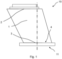
- Figure 1 shows an example of a mini-LED device 10.
- the product's first (top) surface side 2 contains pads that need to be aligned with the substrate pad 11 when placed.
- the second (bottom) surface side 3 of the product 10 is 'obscured' with a piece of sapphire 1, which is different on the top surface side 2 and on the bottom surface side 3 due to its slanted nature. Alignment of the pads on the top surface side 2 by measuring the bottom surface 3 side is therefore not possible.
- Figure 1 shows a schematic view of a sapphire 1 aligned with a substrate pad 11 (or the placing area 4). It may be seen that a top surface side 2 is not directly over the substrate pad 11. The alignment situation in which the top surface side 2 is directly over the substrate pad 11 is shown in Figure 2 , but in this case a bottom surface side 3 is not aligned with the substrate pad 11 on the placing area 4 thus resulting in an incorrect assembly.
- any other type of semiconductor component 10 can be used, preferably a silicon semiconductor component. Both examples can be used for visible and near infrared light sources
- the electronic component 10 can be placed on an integrated circuit substrate 11.
- a transfer substrate 11 can be used in particular in LED applications.
- the disclosure presents a method to provide a correct assembly while position an electronic component 10 while assembling is performed while only a top, first surface side 2 of the electronic component is visible.
- a method is performed on an electronic component 10 having a first, top surface side 2 and a second, bottom surface side 3 opposite to the first surface side 2.
- the electronic component 10 is illuminated, by means of a light source unit, with light which transmits through the electronic component 10, such that at least one feature of the electronic component 10 visible from the first surface side 2 and at least one feature 5 visible from the second surface side 3.
- step b an image of the electronic component 10 is obtained with a first camera unit.
- the image contains image data of the at least one feature present 5 visible from the first surface side 2 and at least one feature 5 visible from the second surface side 3.
- a correction value is calculated. This calculations are based on the image data from the image taken in the second step.
- the correction value is indicative of a position of the second surface side 3 of the electronic component 1 with respect to the first surface side 2 of the electronic component 10.
- the correction value is an offset, which informs how misaligned a first, top side 2 of the electronic component 10 has to be so that the second, bottom side 3 is placed in a designated place 4.
- step d the electronic component 10 is transferred to an assembling station. It should be noted that it is possible to perform all steps in one station which is able to take pictures, calculate and assembly. In such case the fourth step take place before a final assembly.
- step e a position of an adjusted placing area 4 of the electronic component 10 is calculated. It is done by adjusting a placing area 4, which is an area within the assembling station where the second side 3 of the electronic component 10 must by placed, with the correction value. This step may also be performed step d.
- step f the electronic component 10 is placed in the designated place 4.
- a second camera unit is used to keep track of the first, top surface side 2.
- the position information obtained from the image is directly correlated with the top side of the product.
- Alignment is performed based on internal structures 5 of a semiconductor product, instead of external (surface) structures. This is particularly useful for mini-LED and micro-LED product alignment, because of the extreme rough surface edges and the significant slanted sidewall edges which cannot be used for robust alignment.
- the light source unit emits light in the infrared or in the visible wavelength spectrum.
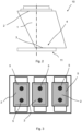
- Figure 3 shows three mini-LED products imaged through a sapphire top layer. Sapphire has a high transmission for visible light, so illuminating and imaging the product in visible light, in this case blue light with a wavelength of 457 nm, produced the highest contrast between the pads of the device and the rest of the image.
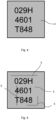
- Figure 4 shows a product image captured from the backside with visible light. Notice that no structures other than the rough outside edge of the product containing a serial number of the electronic component are visible here.
- Figure 5 shows the same product as in Figure 4 , now captured using near-infrared illumination. The internal features 5 become detectable and can be used for product alignment.
- the electronic component 10 is positioned between the light source unit and the first camera unit.
- the first camera unit is capturing light which passed through the electronic component 10.
- the light source unit and the first camera unit are pointing towards the same direction.
- the first camera unit is receiving a light which has been reflected from features of at least one feature 5 visible from the second surface side 3.
- a vision system is used consisting of a camera, optics and an illumination unit with a specific wavelength for which the obscuring part of the semiconductor product is highly transmissive, while at the same time reflective on the internal (metal) structures. This will make the internal structures visible in the captured image and available for alignment on a substrate.
- the position can be found via template matching, in which a reference image of the expected feature is defined as template and matched on every runtime captured image.
- the internal structures which are used as features to align on are typically low contrast and are only partly visible.
- a more advanced alignment technique based on a neural network can be used which is less sensitive for low contrast and occlusion of varying parts defined in a template reference.
- an axis of the first camera unit and/or the second camera unit is perpendicular to the first surface side 2 and/or the second surface side 3 of the electronic component 10.
- a plane of the first surface side 2 is perpendicular to the axis of the first camera unit and thus results in fewer image processing operation needed.
- this method may be used to place the electronic component 10 on an integrated circuit substrate.
- the electronic component 10 may be a sapphire component 1.
- the electronic component 10 may also be any other type of semiconductor component, preferably a silicon semiconductor component.
- a transfer substrate 11 can be used in particular in LED applications. Both examples can be used for visible and near infrared light sources.
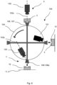
- the system 100 comprising a light source unit 101, a first camera unit 102, a second camera unit 103, a transportation unit 104, and a processing system (not shown).
- the first camera unit 102 is configured to obtain an image of the second surface side 3 of the electronic component 10 in a first measuring position X.
- the second camera unit 103 is configured to obtain an image of the first surface side 2 of the electronic component 10 in a second measuring position Y.
- the transportation unit 104 is configured to transport the electronic component 10 from the first measuring position X to the second measuring position Y.
- the processing system is configured to calculate, based on the image data, of a correction value wherein the correction value is indicative a position of the second surface side 3 of the electronic component 10 with respect to the first surface side 2 of the electronic component 10, and to calculate of position of an adjusted placing area of the electronic component 10 by adjusting a placing area 4, which is an area within the second measuring position Y where the second surface side 3 of the electronic component 10 must by placed on the designated place 4, with the correction value.
- the measuring of the first measuring position (for performing steps a, b) and the second measuring position (for performing step f) may take place in one space (for example in one device) which space (device) is configured to perform all tasks in one place.
- system 100 may also comprise a measuring unit 106 configured to hold the electronic component 10 in the first measuring position X.
- system 100 also comprises a holding unit 107 configured to hold the electronic component 10 in the second measuring position Y.
- the system 100 comprises an assembly device 108 configured to place the electronic component 10 on the placing area 4.
- the assembly device 108 may be, for example, a robotic arm 108a.
- the light source unit 102 emits an infrared light or a visible light.
- a type of the light depends on properties of a particular electronic device 10 to be placed.
- the measuring unit 106 is configured to hold the electronic component 10 between the light source unit 102 and the first camera unit 103.
- the first camera unit 102 is capturing light which passed through the electronic component 10.
- the light source unit 102 and the first camera unit 103 are pointing towards the same direction.
- the first camera unit 102 is receiving a light which has been reflected from features of at least one feature 5 visible from the second surface side 3.
- an axis 102z of the first camera unit 102 and/or an axis 103z of the second camera unit 103 is perpendicular to the first surface side 2 and/or the second surface side 3 of the electronic component 10.
- the measuring of the second measuring position can be performed either before or after the placement of the electronic component 10 on the substrate in the placing area 4, According, the second measuring position can be determined either while the electronic component 10 is still held by the transportation unit 104 or when the electronic component 10 is already placed on the substrate. At stated previously. both situations may depend on the alignment requirements of the specific application.
- the electronics side 2 of the electronic product 10 can be inspected prior to the placement on the substrate, whilst the electronic component is being held by the transportation unit 104. Accordingly, with the second measuring position Y and the correction value thus obtained prior to placement, proper alignment of the electronic product 10 with its second surface side 3 on the substrate on the placing area 4 can be achieved.
- the placement of the electronic product 10 on the substrate in the placing area 4 may need validation after the placement. Accordingly, a correction value is associated with the (non-aligning) features on the top side 2 in order to determine the actual placement position of the electronics on the other side of the electronic product relative to the substrate 11.
Landscapes
- Engineering & Computer Science (AREA)
- Computer Vision & Pattern Recognition (AREA)
- Physics & Mathematics (AREA)
- General Physics & Mathematics (AREA)
- Theoretical Computer Science (AREA)
- Quality & Reliability (AREA)
- Supply And Installment Of Electrical Components (AREA)
- Container, Conveyance, Adherence, Positioning, Of Wafer (AREA)
- Length Measuring Devices By Optical Means (AREA)
- Wire Bonding (AREA)
- Die Bonding (AREA)
- Led Device Packages (AREA)
- Led Devices (AREA)
- Manufacturing & Machinery (AREA)
Abstract
Description
- The present disclosure relates to a technology of aligning electronic components during manufacturing, especially semiconductor components with an irregular shape.
- When aligning electronic components in semiconductor pick-and-place applications, the bottom side alignment is normally based on outer physical edges of the component. Because of variance in the dicing process this alignment has no direct correlation with any structures present on the top surface of the component. These outer physical edges can also show a high roughness caused by the applied dicing process which has large impact on the alignment precision. In addition, the product sidewall can show significant slanted sides which varies from product to product, so that the top and bottom surfaces are not aligned.
- Typically a semiconductor pick-and-place assembly equipment aligned products based on visual structures on the surface of the semiconductor devices. When alignment was needed between top and bottom of these devices, alignment structures were required that are visible on both sides of the product. In practise this often meant aligning on the outer edge of the product, as most devices have a straight edge (parallel to the camera viewing axis).
- Prior art made use of external structures for alignment, mostly the outer physical edges of a product. As these features are not always present on both sides of a semiconductor product, alignment on structures at the other side of the product than the one imaged is not always possible.
- Document
US8750597B2 discloses a method of performing inspection alignment point selection for semiconductor devices includes importing, with a computer device, one or more semiconductor design files corresponding to an area of a semiconductor die; aligning a design taken from the one or more semiconductor design files with an image taken from a die of a semiconductor wafer; and selecting an alignment point and recording a portion of the design file corresponding to the alignment point as a master reference image. - Document
US6185816B1 discloses a system for handling semiconductor workpieces, by aligning a movable pick and place device and a movable optical control device, is disclosed. The system and method provide for the formation of an imprint by the pick and place device. The optical control device can then be aligned to that imprint, creating alignment between the pick and place device and the optical control device. Once alignment is complete the imprinted material may be replaced with one or more semiconductor workpieces. - Accordingly, it is a goal of the present disclosure to provide an improved alignment method which may be used in cases, where features on a top surface of the semiconductor component or device are not sufficient due to process limitations and where a bottom surface might also not show any alignment correlation with the top surface.
- According to a first example of the disclosure, a method of aligning and placing an electronic component is proposed, with the electronic component having a first, top surface side and a second, bottom surface side opposite to the first surface side. The method comprises steps of illuminating, using a light source unit, the electronic component with light which transmits through the electronic component, such that at least one feature of the electronic component visible from the first surface side and at least one feature visible from the second surface side; obtaining, using a first camera unit, an image of the electronic component containing image data of the at least one feature present visible from the first surface side and at least one feature visible from the second surface side; calculating, based on the image data, of a correction value wherein the correction value is indicative of a position of the second surface side of the electronic component with respect to the first surface side of the electronic component; transferring the electronic component to an assembling station; calculating of a position of an adjusted placing area of the electronic component by adjusting a placing area, which is an area within the assembling station where the second side of the electronic component must by placed, with the correction value; placing the semiconductor component, using a second camera unit, by obtaining an image containing image data of the first surface side of the electronic component and an assembly device structured to place the electronic component, such that the first surface side of the electronic component is located within the adjusted designated area.
- Preferably the light source unit emits light in the infrared or in the visible wavelength spectrum.
- Preferably in step a. and b. the electronic component is positioned between the light source unit and the first camera unit.
- Preferably in step a. and b. the light source unit and the first camera unit are pointing towards the same direction.
- Preferably in step c a template matching algorithm or one or more machine learning algorithms is used.
- Preferably an axis of the first camera unit and/or the second camera unit is perpendicular to the first surface side and/or the second surface side of the electronic component.
- In an non-limiting example, the electronic component is placed on an integrated circuit substrate. Alternatively, a transfer substrate can be used in particular in LED applications.
- Furthermore, in a non-limiting example, the electronic component is a sapphire component. However, any other type of semiconductor component can be used, such as a silicon semiconductor component. Both examples can be used for visible and near infrared light sources.
- According to a further example of the disclosure a system for aligning and placing an electronic component is disclosed. The system comprising a light source unit, a first camera unit configured to obtain an image of an electronic component in a first measuring position, the electronic component having a first, top surface side and a second, bottom surface side opposite to the first surface side, the image containing image data of the at least one feature visible from the first surface side and at least one electronic feature visible from the second surface side, a second camera unit configured to obtain an image of the first surface side of the electronic component in a second measuring position, a transportation unit configured to transport the electronic component from the first measuring position to the second measuring position, a processing system configured to calculate, based on the image data, of a correction value wherein the correction value is indicative a position of the second surface side of the electronic component with respect to the first surface side of the electronic component, and to calculate of position of an adjusted placing area of the electronic component by adjusting a placing area, which is an area within the second measuring position where the second side of the electronic component must by placed, with the correction value.
- It should be noted, that the measuring of the second measuring position can be performed either before or after the placement of the electronic component on the substrate, That is either while the electronic component is still held by the transportation unit or when the electronic component is already placed on the substrate. Both situations may depend on the alignment requirements of the specific application.
- In the first situation, the electronics side of the electronic product can be inspected prior to the placement on the substrate, whilst the electronic component is being held by the transportation unit. Accordingly, with the second measuring position and the correction value thus obtained prior to placement, proper alignment of the electronic product on the substrate can be achieved.
- In the second situation, the placement of the electronic product on the substrate may need validation after the placement. Accordingly, a correction value is associated with the (non-aligning) features on the top side in order to determine the actual placement position of the electronics on the other side of the electronic product relative to the substrate.
- Preferably the system also comprising a measuring unit configured to hold the electronic component in the first measuring position.
- Preferably the system also comprising a holding unit configured to hold the electronic component in the second measuring position.
- Preferably the system also comprising an assembly device configured to place the electronic component on the placing area.
- Preferably the light source emits an infrared light or a visible light.
- Preferably the measuring unit is configured to hold the electronic component between the light source unit and the first camera unit.
- Preferably the light source unit and the first camera unit are pointing toward the same direction.
- Preferably an axis of the first camera unit and/or the second camera unit is perpendicular to the first surface side and/or the second surface side of the electronic component.
- The disclosure will now be discussed with reference to the drawings, which show in:
-
Figure 1 an example of a mini-LED device in particlar a schematic view of the sapphire part of a mini-LED device aligned with a substrate pad, -
Figure 2 a schematic view of the electronics part of a mini-LED device aligned with a substrate pad, -
Figure 3 three mini-LED products imaged through a sapphire top layer, -
Figure 4 a product image captured from the backside with visible light, -
Figure 5 a product image captured from the backside with infrared light, -
Figure 6 a system for aligning and placing an electronic component. - For a proper understanding of the disclosure, in the detailed description below corresponding elements or parts of the disclosure will be denoted with identical reference numerals in the drawings.
-
Figure 1 shows an example of amini-LED device 10. The product's first (top)surface side 2 contains pads that need to be aligned with thesubstrate pad 11 when placed. However, the second (bottom)surface side 3 of theproduct 10 is 'obscured' with a piece ofsapphire 1, which is different on thetop surface side 2 and on thebottom surface side 3 due to its slanted nature. Alignment of the pads on thetop surface side 2 by measuring thebottom surface 3 side is therefore not possible. - In particular, but in a non-limiting example,
Figure 1 shows a schematic view of asapphire 1 aligned with a substrate pad 11 (or the placing area 4). It may be seen that atop surface side 2 is not directly over thesubstrate pad 11. The alignment situation in which thetop surface side 2 is directly over thesubstrate pad 11 is shown inFigure 2 , but in this case abottom surface side 3 is not aligned with thesubstrate pad 11 on theplacing area 4 thus resulting in an incorrect assembly. Alternatively, any other type ofsemiconductor component 10 can be used, preferably a silicon semiconductor component. Both examples can be used for visible and near infrared light sources - The
electronic component 10 can be placed on anintegrated circuit substrate 11. Alternatively, atransfer substrate 11 can be used in particular in LED applications. The disclosure presents a method to provide a correct assembly while position anelectronic component 10 while assembling is performed while only a top,first surface side 2 of the electronic component is visible. - A method is performed on an
electronic component 10 having a first,top surface side 2 and a second,bottom surface side 3 opposite to thefirst surface side 2. In a first step, step a, theelectronic component 10 is illuminated, by means of a light source unit, with light which transmits through theelectronic component 10, such that at least one feature of theelectronic component 10 visible from thefirst surface side 2 and at least onefeature 5 visible from thesecond surface side 3. - In a second step, step b, an image of the
electronic component 10 is obtained with a first camera unit. The image contains image data of the at least one feature present 5 visible from thefirst surface side 2 and at least onefeature 5 visible from thesecond surface side 3. - During a third step, step c, a correction value is calculated. This calculations are based on the image data from the image taken in the second step. The correction value is indicative of a position of the
second surface side 3 of theelectronic component 1 with respect to thefirst surface side 2 of theelectronic component 10. In other word the correction value is an offset, which informs how misaligned a first,top side 2 of theelectronic component 10 has to be so that the second,bottom side 3 is placed in a designatedplace 4. - In a fourth step, step d, the
electronic component 10 is transferred to an assembling station. It should be noted that it is possible to perform all steps in one station which is able to take pictures, calculate and assembly. In such case the fourth step take place before a final assembly. - During a next step, step e, a position of an adjusted
placing area 4 of theelectronic component 10 is calculated. It is done by adjusting aplacing area 4, which is an area within the assembling station where thesecond side 3 of theelectronic component 10 must by placed, with the correction value. This step may also be performed step d. - In a final step, step f, the
electronic component 10 is placed in the designatedplace 4. A second camera unit is used to keep track of the first,top surface side 2. By obtaining an image containing image data of thefirst surface side 2 of theelectronic component 10 and an assembly device structured to place theelectronic component 1, such that thefirst surface side 2 of theelectronic component 10 is located within the adjusted designated area. - The position information obtained from the image is directly correlated with the top side of the product.
- Alignment is performed based on
internal structures 5 of a semiconductor product, instead of external (surface) structures. This is particularly useful for mini-LED and micro-LED product alignment, because of the extreme rough surface edges and the significant slanted sidewall edges which cannot be used for robust alignment. - In one example the light source unit emits light in the infrared or in the visible wavelength spectrum.
Figure 3 shows three mini-LED products imaged through a sapphire top layer. Sapphire has a high transmission for visible light, so illuminating and imaging the product in visible light, in this case blue light with a wavelength of 457 nm, produced the highest contrast between the pads of the device and the rest of the image.Figure 4 shows a product image captured from the backside with visible light. Notice that no structures other than the rough outside edge of the product containing a serial number of the electronic component are visible here.Figure 5 shows the same product as inFigure 4 , now captured using near-infrared illumination. Theinternal features 5 become detectable and can be used for product alignment. - In another example, in step a. and b. the
electronic component 10 is positioned between the light source unit and the first camera unit. The first camera unit is capturing light which passed through theelectronic component 10. In another example, in step a. and b. the light source unit and the first camera unit are pointing towards the same direction. In this case the first camera unit is receiving a light which has been reflected from features of at least onefeature 5 visible from thesecond surface side 3. A vision system is used consisting of a camera, optics and an illumination unit with a specific wavelength for which the obscuring part of the semiconductor product is highly transmissive, while at the same time reflective on the internal (metal) structures. This will make the internal structures visible in the captured image and available for alignment on a substrate. - Preferably, in step c, the position can be found via template matching, in which a reference image of the expected feature is defined as template and matched on every runtime captured image. The internal structures which are used as features to align on are typically low contrast and are only partly visible. To optimize alignment robustness a more advanced alignment technique based on a neural network can be used which is less sensitive for low contrast and occlusion of varying parts defined in a template reference.
- In a further example an axis of the first camera unit and/or the second camera unit is perpendicular to the
first surface side 2 and/or thesecond surface side 3 of theelectronic component 10. In this case a plane of thefirst surface side 2 is perpendicular to the axis of the first camera unit and thus results in fewer image processing operation needed. - Preferably this method may be used to place the
electronic component 10 on an integrated circuit substrate. - As stated hereinbefore the
electronic component 10 may be asapphire component 1. Theelectronic component 10 may also be any other type of semiconductor component, preferably a silicon semiconductor component. Alternatively, atransfer substrate 11 can be used in particular in LED applications. Both examples can be used for visible and near infrared light sources. - Also a system for aligning and placing an electronic component is disclosed in
Figure 6 . Thesystem 100 comprising alight source unit 101, afirst camera unit 102, asecond camera unit 103, atransportation unit 104, and a processing system (not shown). Thefirst camera unit 102 is configured to obtain an image of thesecond surface side 3 of theelectronic component 10 in a first measuring position X. Thesecond camera unit 103 is configured to obtain an image of thefirst surface side 2 of theelectronic component 10 in a second measuring position Y. Thetransportation unit 104 is configured to transport theelectronic component 10 from the first measuring position X to the second measuring position Y. The processing system is configured to calculate, based on the image data, of a correction value wherein the correction value is indicative a position of thesecond surface side 3 of theelectronic component 10 with respect to thefirst surface side 2 of theelectronic component 10, and to calculate of position of an adjusted placing area of theelectronic component 10 by adjusting aplacing area 4, which is an area within the second measuring position Y where thesecond surface side 3 of theelectronic component 10 must by placed on the designatedplace 4, with the correction value. - In an example of the
system 100 the measuring of the first measuring position (for performing steps a, b) and the second measuring position (for performing step f) may take place in one space (for example in one device) which space (device) is configured to perform all tasks in one place. - In one example the
system 100 may also comprise ameasuring unit 106 configured to hold theelectronic component 10 in the first measuring position X. - In another example the
system 100 also comprises a holdingunit 107 configured to hold theelectronic component 10 in the second measuring position Y. - In yet another example the
system 100 comprises an assembly device 108 configured to place theelectronic component 10 on theplacing area 4. The assembly device 108 may be, for example, a robotic arm 108a. - It should be noted, that the
light source unit 102 emits an infrared light or a visible light. A type of the light depends on properties of a particularelectronic device 10 to be placed. - In another example, the measuring
unit 106 is configured to hold theelectronic component 10 between thelight source unit 102 and thefirst camera unit 103. Thefirst camera unit 102 is capturing light which passed through theelectronic component 10. In another example thelight source unit 102 and thefirst camera unit 103 are pointing towards the same direction. In this case thefirst camera unit 102 is receiving a light which has been reflected from features of at least onefeature 5 visible from thesecond surface side 3. - In one example an
axis 102z of thefirst camera unit 102 and/or anaxis 103z of thesecond camera unit 103 is perpendicular to thefirst surface side 2 and/or thesecond surface side 3 of theelectronic component 10. - The measuring of the second measuring position can be performed either before or after the placement of the
electronic component 10 on the substrate in theplacing area 4, According, the second measuring position can be determined either while theelectronic component 10 is still held by thetransportation unit 104 or when theelectronic component 10 is already placed on the substrate. At stated previously. both situations may depend on the alignment requirements of the specific application. First, theelectronics side 2 of theelectronic product 10 can be inspected prior to the placement on the substrate, whilst the electronic component is being held by thetransportation unit 104. Accordingly, with the second measuring position Y and the correction value thus obtained prior to placement, proper alignment of theelectronic product 10 with itssecond surface side 3 on the substrate on theplacing area 4 can be achieved. - In the second situation, the placement of the
electronic product 10 on the substrate in theplacing area 4 may need validation after the placement. Accordingly, a correction value is associated with the (non-aligning) features on thetop side 2 in order to determine the actual placement position of the electronics on the other side of the electronic product relative to thesubstrate 11. -
- 1
- sapphire body
- 2
- first surface
- 3
- second surface
- 4
- placing area
- 5
- feature of the second surface
- 10
- electronic component
- 11
- substrate
- 100
- system
- 101
- light source unit
- 102
- first camera unit
- 102z
- axis of first camera unit
- 103
- second camera unit
- 103z
- axis of second camera unit
- 104
- transportation unit
- 106
- measuring unit
- 107
- holding unit
- 108
- assembly device
- 108a
- robotic arm
Claims (15)
- A method of aligning and placing an electronic component, the electronic component (10) having a first, top surface side (2) and a second, bottom surface side (3) opposite to the first surface side (2), the method comprising steps ofa. illuminating, using a light source unit, the electronic component (10) with light which transmits through the electronic component (10), such that at least one feature of the electronic component (10) visible from the first surface side and at least one feature (5) visible from the second surface side;b. obtaining, using a first camera unit, an image of the electronic component (10) containing image data of the at least one feature present visible from the first surface side (2) and at least one feature (5) visible from the second surface side;c. calculating, based on the image data, of a correction value wherein the correction value is indicative of a position of the second surface side (3) of the electronic component (10) with respect to the first surface side (2) of the electronic component (10);d. transferring the electronic component to an assembling station;e. calculating of a position of an adjusted placing area (4) of the electronic component (10) by adjusting a placing area (4), which is an area within the assembling station where the second side (3) of the electronic component (10) must by placed, with the correction value;f. placing the electronic component (10), using a second camera unit, by obtaining an image containing image data of the first surface side (2) of the electronic component (10) and an assembly device structured to place the electronic component (10), such that the first surface side (2) of the electronic component (10) is located within the adjusted designated area.
- The method according to claim 1, wherein the light source unit emits light in the infrared or in the visible wavelength spectrum.
- The method according to claim 1 or 2, wherein in step a. and b. the electronic component (10) is positioned between the light source unit and the first camera unit.
- The method according to claim 1 or 2, wherein in step a. and b. the light source unit and the first camera unit are pointing towards the same direction.
- The method according to any one or more of claims 1-4, wherein in step c a temple matching algorithm or one or more machine learning algorithms is used.
- The method according to any one or more of the claims 1-5, wherein an axis of the first camera unit and/or the second camera unit is perpendicular to the first surface side (2) and/or the second surface side (3) of the electronic component (10).
- The method according to anyone of claims 1-6, wherein the electronic component (10) is placed on an integrated circuit substrate.
- The method according to anyone of claims 1-7, wherein the electronic component (10) is a sapphire component or any other type of semiconductor component, preferably a silicon semiconductor component.
- A system for aligning and placing an electronic component comprising:a light source unit,a first camera unit configured to obtain an image of an electronic component (10) in a first measuring position, the electronic component (10) having a first, top surface side (2) and a second, bottom surface side (3) opposite to the first surface side, the image containing image data of the at least one feature visible from the first surface side and at least one feature (5) visible from the second surface side;a second camera unit configured to obtain an image of the first surface side (2) of the electronic component (10) in a second measuring position;a transportation unit configured to transport the electronic component (10) from the first measuring position to the second measuring position;a processing system configured to calculate, based on the image data, of a correction value wherein the correction value is indicative a position of the second surface side (3) of the electronic component (10) with respect to the first surface side (2) of the electronic component (10), and to calculate of position of an adjusted placing area of the electronic component (10) by adjusting a placing area (4), which is an area within the second measuring position where the second side (3) of the electronic component must by placed, with the correction value.
- The system according to claim 9, further comprising a measuring unit configured to hold the electronic component (10) in the first measuring position.
- The system according to claim 9 or 10, further comprising a holding unit configured to hold the electronic component (10) in the second measuring position.
- The system according to any one or more of the claims 9-11, further comprising an assembly device configured to place the electronic component (10) on the placing area (4).
- The system according to any one or more of the claims 9-12, wherein the measuring unit is configured to hold the electronic component (10) between the light source unit and the first camera unit.
- The system according to any one or more of the claims 9-13, wherein the light source unit and the first camera unit are pointing toward the same direction.
- The system according to any one or more of the claims 9-14, wherein an axis of the first camera unit and/or the second camera unit is perpendicular to the first surface side (2) and/or the second surface side (3) of the electronic component (10).
Priority Applications (6)
| Application Number | Priority Date | Filing Date | Title |
|---|---|---|---|
| EP22151055.5A EP4210090B1 (en) | 2022-01-11 | 2022-01-11 | A method of aligning and placing an electronic component and a system for aligning and placing an electronic component |
| CN202310037480.8A CN116435240A (en) | 2022-01-11 | 2023-01-09 | Method and system for aligning and placing electronic components |
| TW112100812A TW202405760A (en) | 2022-01-11 | 2023-01-09 | A method of aligning and placing an electronic component and a system for aligning and placing an electronic component |
| KR1020230002715A KR20230108711A (en) | 2022-01-11 | 2023-01-09 | A method of aligning and placing an electronic component and a system for aligning and placing an electronic component |
| JP2023001592A JP2023102279A (en) | 2022-01-11 | 2023-01-10 | Electronic component alignment method and electronic component alignment system |
| US18/152,834 US12482680B2 (en) | 2022-01-11 | 2023-01-11 | Method of aligning and placing an electronic component and a system for aligning and placing an electronic component |
Applications Claiming Priority (1)
| Application Number | Priority Date | Filing Date | Title |
|---|---|---|---|
| EP22151055.5A EP4210090B1 (en) | 2022-01-11 | 2022-01-11 | A method of aligning and placing an electronic component and a system for aligning and placing an electronic component |
Publications (2)
| Publication Number | Publication Date |
|---|---|
| EP4210090A1 true EP4210090A1 (en) | 2023-07-12 |
| EP4210090B1 EP4210090B1 (en) | 2024-10-30 |
Family
ID=79317187
Family Applications (1)
| Application Number | Title | Priority Date | Filing Date |
|---|---|---|---|
| EP22151055.5A Active EP4210090B1 (en) | 2022-01-11 | 2022-01-11 | A method of aligning and placing an electronic component and a system for aligning and placing an electronic component |
Country Status (6)
| Country | Link |
|---|---|
| US (1) | US12482680B2 (en) |
| EP (1) | EP4210090B1 (en) |
| JP (1) | JP2023102279A (en) |
| KR (1) | KR20230108711A (en) |
| CN (1) | CN116435240A (en) |
| TW (1) | TW202405760A (en) |
Citations (5)
| Publication number | Priority date | Publication date | Assignee | Title |
|---|---|---|---|---|
| US6185816B1 (en) | 1999-07-06 | 2001-02-13 | Lucent Technologies Inc. | Alignment method |
| US6389688B1 (en) * | 1997-06-18 | 2002-05-21 | Micro Robotics Systems, Inc. | Method and apparatus for chip placement |
| US8750597B2 (en) | 2011-11-23 | 2014-06-10 | International Business Machines Corporation | Robust inspection alignment of semiconductor inspection tools using design information |
| US20150237309A1 (en) * | 2014-02-14 | 2015-08-20 | Asm Assembly Systems Gmbh & Co. Kg | Optical measurement of a component having structural features present at opposite sides |
| US20150358558A1 (en) * | 2014-06-04 | 2015-12-10 | Flir Systems, Inc. | Wafer level packaging of reduced-height infrared detectors |
Family Cites Families (10)
| Publication number | Priority date | Publication date | Assignee | Title |
|---|---|---|---|---|
| JPH0642501B2 (en) * | 1987-12-18 | 1994-06-01 | 富士通株式会社 | Positioning method for small semiconductor chips |
| US7842912B2 (en) * | 2008-05-23 | 2010-11-30 | Delta Design, Inc. | Camera based vision alignment with device group guiding for semiconductor device testing handlers |
| US8318512B2 (en) * | 2009-04-29 | 2012-11-27 | Applied Materials, Inc. | Automated substrate handling and film quality inspection in solar cell processing |
| US8633441B2 (en) * | 2009-09-02 | 2014-01-21 | Asm Assembly Automation Ltd | Die bonding process incorporating infrared vision system |
| CN115719721A (en) * | 2016-08-29 | 2023-02-28 | Ev 集团 E·索尔纳有限责任公司 | Method and apparatus for aligning a substrate |
| JP7097691B2 (en) * | 2017-12-06 | 2022-07-08 | 東京エレクトロン株式会社 | Teaching method |
| US12148181B2 (en) * | 2020-08-28 | 2024-11-19 | Canon Kabushiki Kaisha | Measurement apparatus that measures position information of measurement target in predetermined direction |
| KR102822419B1 (en) * | 2020-12-08 | 2025-06-18 | 에스케이하이닉스 주식회사 | Semiconductor manufacturing equipment, method of reading position of carrier and method of attaching semiconductor die on carrier using semiconductor manufacturing equipment |
| KR102807827B1 (en) * | 2021-08-27 | 2025-05-15 | 삼성전자주식회사 | Teaching apparatus and substrate alignment apparatus using the same |
| WO2023110114A1 (en) * | 2021-12-17 | 2023-06-22 | Ev Group E. Thallner Gmbh | Device and method for adjusting a detection means |
-
2022
- 2022-01-11 EP EP22151055.5A patent/EP4210090B1/en active Active
-
2023
- 2023-01-09 CN CN202310037480.8A patent/CN116435240A/en active Pending
- 2023-01-09 TW TW112100812A patent/TW202405760A/en unknown
- 2023-01-09 KR KR1020230002715A patent/KR20230108711A/en active Pending
- 2023-01-10 JP JP2023001592A patent/JP2023102279A/en active Pending
- 2023-01-11 US US18/152,834 patent/US12482680B2/en active Active
Patent Citations (5)
| Publication number | Priority date | Publication date | Assignee | Title |
|---|---|---|---|---|
| US6389688B1 (en) * | 1997-06-18 | 2002-05-21 | Micro Robotics Systems, Inc. | Method and apparatus for chip placement |
| US6185816B1 (en) | 1999-07-06 | 2001-02-13 | Lucent Technologies Inc. | Alignment method |
| US8750597B2 (en) | 2011-11-23 | 2014-06-10 | International Business Machines Corporation | Robust inspection alignment of semiconductor inspection tools using design information |
| US20150237309A1 (en) * | 2014-02-14 | 2015-08-20 | Asm Assembly Systems Gmbh & Co. Kg | Optical measurement of a component having structural features present at opposite sides |
| US20150358558A1 (en) * | 2014-06-04 | 2015-12-10 | Flir Systems, Inc. | Wafer level packaging of reduced-height infrared detectors |
Also Published As
| Publication number | Publication date |
|---|---|
| KR20230108711A (en) | 2023-07-18 |
| EP4210090B1 (en) | 2024-10-30 |
| US20230223286A1 (en) | 2023-07-13 |
| JP2023102279A (en) | 2023-07-24 |
| CN116435240A (en) | 2023-07-14 |
| TW202405760A (en) | 2024-02-01 |
| US12482680B2 (en) | 2025-11-25 |
Similar Documents
| Publication | Publication Date | Title |
|---|---|---|
| EP4435840B1 (en) | Wireless substrate-like teaching sensor for semiconductor processing | |
| KR101200666B1 (en) | Alignment device controller and alignment method | |
| US8582121B2 (en) | Article recognition apparatus and article processing apparatus using the same | |
| US20110234788A1 (en) | Assembly inspection apparatus and assembly processing apparatus using the same | |
| JP5108003B2 (en) | Improvement of image quality by multi-wavelength light | |
| US6064757A (en) | Process for three dimensional inspection of electronic components | |
| EP3711908B1 (en) | Calibration device for robot arm | |
| US20090009755A1 (en) | Method for detecting position of defect on semiconductor wafer | |
| TWI665749B (en) | Test dummy for precision transfer position measurement using the semiconductor system or disply system and precision transfer positon measurement method using the test dummy | |
| US11341357B2 (en) | Medicine inspection device, image processing device, image processing method, and program | |
| US7197176B2 (en) | Mark position detecting apparatus and mark position detecting method | |
| US20220181181A1 (en) | Semiconductor manufacturing apparatus, method of reading position of carrier, and method of attaching semiconductor die on carrier using semiconductor manufacturing apparatus | |
| CN108681209A (en) | Detection device and method, patterning device, acquisition methods and manufacturing method | |
| US20220299317A1 (en) | Method for positioning substrate | |
| EP4210090B1 (en) | A method of aligning and placing an electronic component and a system for aligning and placing an electronic component | |
| US6861186B1 (en) | Method for backside alignment of photo-processes using standard front side alignment tools | |
| US20180114767A1 (en) | Bond head assemblies including reflective optical elements, related bonding machines, and related methods | |
| JP5975668B2 (en) | Work conveying device, work conveying method, and method of manufacturing assembly parts | |
| US20120314050A1 (en) | Imaging apparatus and control method therefor | |
| JP2012185400A (en) | Storage container, device manufacturing apparatus, and device manufacturing method | |
| TWI400020B (en) | Picking-up and placing method with integrated pcb information | |
| JP6371742B2 (en) | Measuring device and acquisition method | |
| JP2018155842A (en) | Measurement method, measurement program, and measurement system | |
| WO2001004567A2 (en) | Method and apparatus for three dimensional inspection of electronic components | |
| CN111473783B (en) | Production line code processing system and method |
Legal Events
| Date | Code | Title | Description |
|---|---|---|---|
| PUAI | Public reference made under article 153(3) epc to a published international application that has entered the european phase |
Free format text: ORIGINAL CODE: 0009012 |
|
| STAA | Information on the status of an ep patent application or granted ep patent |
Free format text: STATUS: THE APPLICATION HAS BEEN PUBLISHED |
|
| AK | Designated contracting states |
Kind code of ref document: A1 Designated state(s): AL AT BE BG CH CY CZ DE DK EE ES FI FR GB GR HR HU IE IS IT LI LT LU LV MC MK MT NL NO PL PT RO RS SE SI SK SM TR |
|
| STAA | Information on the status of an ep patent application or granted ep patent |
Free format text: STATUS: REQUEST FOR EXAMINATION WAS MADE |
|
| 17P | Request for examination filed |
Effective date: 20231222 |
|
| RBV | Designated contracting states (corrected) |
Designated state(s): AL AT BE BG CH CY CZ DE DK EE ES FI FR GB GR HR HU IE IS IT LI LT LU LV MC MK MT NL NO PL PT RO RS SE SI SK SM TR |
|
| GRAP | Despatch of communication of intention to grant a patent |
Free format text: ORIGINAL CODE: EPIDOSNIGR1 |
|
| STAA | Information on the status of an ep patent application or granted ep patent |
Free format text: STATUS: GRANT OF PATENT IS INTENDED |
|
| RIC1 | Information provided on ipc code assigned before grant |
Ipc: H01L 21/67 20060101ALN20240503BHEP Ipc: H01L 21/68 20060101AFI20240503BHEP |
|
| INTG | Intention to grant announced |
Effective date: 20240524 |
|
| GRAS | Grant fee paid |
Free format text: ORIGINAL CODE: EPIDOSNIGR3 |
|
| GRAA | (expected) grant |
Free format text: ORIGINAL CODE: 0009210 |
|
| STAA | Information on the status of an ep patent application or granted ep patent |
Free format text: STATUS: THE PATENT HAS BEEN GRANTED |
|
| AK | Designated contracting states |
Kind code of ref document: B1 Designated state(s): AL AT BE BG CH CY CZ DE DK EE ES FI FR GB GR HR HU IE IS IT LI LT LU LV MC MK MT NL NO PL PT RO RS SE SI SK SM TR |
|
| REG | Reference to a national code |
Ref country code: GB Ref legal event code: FG4D |
|
| REG | Reference to a national code |
Ref country code: CH Ref legal event code: EP |
|
| REG | Reference to a national code |
Ref country code: DE Ref legal event code: R096 Ref document number: 602022007117 Country of ref document: DE |
|
| REG | Reference to a national code |
Ref country code: IE Ref legal event code: FG4D |
|
| REG | Reference to a national code |
Ref country code: LT Ref legal event code: MG9D |
|
| REG | Reference to a national code |
Ref country code: NL Ref legal event code: MP Effective date: 20241030 |
|
| PG25 | Lapsed in a contracting state [announced via postgrant information from national office to epo] |
Ref country code: HR Free format text: LAPSE BECAUSE OF FAILURE TO SUBMIT A TRANSLATION OF THE DESCRIPTION OR TO PAY THE FEE WITHIN THE PRESCRIBED TIME-LIMIT Effective date: 20241030 Ref country code: PT Free format text: LAPSE BECAUSE OF FAILURE TO SUBMIT A TRANSLATION OF THE DESCRIPTION OR TO PAY THE FEE WITHIN THE PRESCRIBED TIME-LIMIT Effective date: 20250228 Ref country code: IS Free format text: LAPSE BECAUSE OF FAILURE TO SUBMIT A TRANSLATION OF THE DESCRIPTION OR TO PAY THE FEE WITHIN THE PRESCRIBED TIME-LIMIT Effective date: 20250228 |
|
| PG25 | Lapsed in a contracting state [announced via postgrant information from national office to epo] |
Ref country code: NL Free format text: LAPSE BECAUSE OF FAILURE TO SUBMIT A TRANSLATION OF THE DESCRIPTION OR TO PAY THE FEE WITHIN THE PRESCRIBED TIME-LIMIT Effective date: 20241030 Ref country code: FI Free format text: LAPSE BECAUSE OF FAILURE TO SUBMIT A TRANSLATION OF THE DESCRIPTION OR TO PAY THE FEE WITHIN THE PRESCRIBED TIME-LIMIT Effective date: 20241030 |
|
| REG | Reference to a national code |
Ref country code: AT Ref legal event code: MK05 Ref document number: 1737803 Country of ref document: AT Kind code of ref document: T Effective date: 20241030 |
|
| PG25 | Lapsed in a contracting state [announced via postgrant information from national office to epo] |
Ref country code: BG Free format text: LAPSE BECAUSE OF FAILURE TO SUBMIT A TRANSLATION OF THE DESCRIPTION OR TO PAY THE FEE WITHIN THE PRESCRIBED TIME-LIMIT Effective date: 20241030 |
|
| PG25 | Lapsed in a contracting state [announced via postgrant information from national office to epo] |
Ref country code: ES Free format text: LAPSE BECAUSE OF FAILURE TO SUBMIT A TRANSLATION OF THE DESCRIPTION OR TO PAY THE FEE WITHIN THE PRESCRIBED TIME-LIMIT Effective date: 20241030 |
|
| PG25 | Lapsed in a contracting state [announced via postgrant information from national office to epo] |
Ref country code: NO Free format text: LAPSE BECAUSE OF FAILURE TO SUBMIT A TRANSLATION OF THE DESCRIPTION OR TO PAY THE FEE WITHIN THE PRESCRIBED TIME-LIMIT Effective date: 20250130 |
|
| PG25 | Lapsed in a contracting state [announced via postgrant information from national office to epo] |
Ref country code: AT Free format text: LAPSE BECAUSE OF FAILURE TO SUBMIT A TRANSLATION OF THE DESCRIPTION OR TO PAY THE FEE WITHIN THE PRESCRIBED TIME-LIMIT Effective date: 20241030 Ref country code: GR Free format text: LAPSE BECAUSE OF FAILURE TO SUBMIT A TRANSLATION OF THE DESCRIPTION OR TO PAY THE FEE WITHIN THE PRESCRIBED TIME-LIMIT Effective date: 20250131 Ref country code: LV Free format text: LAPSE BECAUSE OF FAILURE TO SUBMIT A TRANSLATION OF THE DESCRIPTION OR TO PAY THE FEE WITHIN THE PRESCRIBED TIME-LIMIT Effective date: 20241030 |
|
| PG25 | Lapsed in a contracting state [announced via postgrant information from national office to epo] |
Ref country code: PL Free format text: LAPSE BECAUSE OF FAILURE TO SUBMIT A TRANSLATION OF THE DESCRIPTION OR TO PAY THE FEE WITHIN THE PRESCRIBED TIME-LIMIT Effective date: 20241030 |
|
| PG25 | Lapsed in a contracting state [announced via postgrant information from national office to epo] |
Ref country code: RS Free format text: LAPSE BECAUSE OF FAILURE TO SUBMIT A TRANSLATION OF THE DESCRIPTION OR TO PAY THE FEE WITHIN THE PRESCRIBED TIME-LIMIT Effective date: 20250130 |
|
| PG25 | Lapsed in a contracting state [announced via postgrant information from national office to epo] |
Ref country code: SM Free format text: LAPSE BECAUSE OF FAILURE TO SUBMIT A TRANSLATION OF THE DESCRIPTION OR TO PAY THE FEE WITHIN THE PRESCRIBED TIME-LIMIT Effective date: 20241030 |
|
| PG25 | Lapsed in a contracting state [announced via postgrant information from national office to epo] |
Ref country code: DK Free format text: LAPSE BECAUSE OF FAILURE TO SUBMIT A TRANSLATION OF THE DESCRIPTION OR TO PAY THE FEE WITHIN THE PRESCRIBED TIME-LIMIT Effective date: 20241030 |
|
| PG25 | Lapsed in a contracting state [announced via postgrant information from national office to epo] |
Ref country code: EE Free format text: LAPSE BECAUSE OF FAILURE TO SUBMIT A TRANSLATION OF THE DESCRIPTION OR TO PAY THE FEE WITHIN THE PRESCRIBED TIME-LIMIT Effective date: 20241030 |
|
| PG25 | Lapsed in a contracting state [announced via postgrant information from national office to epo] |
Ref country code: RO Free format text: LAPSE BECAUSE OF FAILURE TO SUBMIT A TRANSLATION OF THE DESCRIPTION OR TO PAY THE FEE WITHIN THE PRESCRIBED TIME-LIMIT Effective date: 20241030 |
|
| PG25 | Lapsed in a contracting state [announced via postgrant information from national office to epo] |
Ref country code: SK Free format text: LAPSE BECAUSE OF FAILURE TO SUBMIT A TRANSLATION OF THE DESCRIPTION OR TO PAY THE FEE WITHIN THE PRESCRIBED TIME-LIMIT Effective date: 20241030 |
|
| PG25 | Lapsed in a contracting state [announced via postgrant information from national office to epo] |
Ref country code: CZ Free format text: LAPSE BECAUSE OF FAILURE TO SUBMIT A TRANSLATION OF THE DESCRIPTION OR TO PAY THE FEE WITHIN THE PRESCRIBED TIME-LIMIT Effective date: 20241030 |
|
| PG25 | Lapsed in a contracting state [announced via postgrant information from national office to epo] |
Ref country code: IT Free format text: LAPSE BECAUSE OF FAILURE TO SUBMIT A TRANSLATION OF THE DESCRIPTION OR TO PAY THE FEE WITHIN THE PRESCRIBED TIME-LIMIT Effective date: 20241030 |
|
| REG | Reference to a national code |
Ref country code: DE Ref legal event code: R097 Ref document number: 602022007117 Country of ref document: DE |
|
| REG | Reference to a national code |
Ref country code: CH Ref legal event code: PL |
|
| PLBE | No opposition filed within time limit |
Free format text: ORIGINAL CODE: 0009261 |
|
| STAA | Information on the status of an ep patent application or granted ep patent |
Free format text: STATUS: NO OPPOSITION FILED WITHIN TIME LIMIT |
|
| PG25 | Lapsed in a contracting state [announced via postgrant information from national office to epo] |
Ref country code: SE Free format text: LAPSE BECAUSE OF FAILURE TO SUBMIT A TRANSLATION OF THE DESCRIPTION OR TO PAY THE FEE WITHIN THE PRESCRIBED TIME-LIMIT Effective date: 20241030 |
|
| PG25 | Lapsed in a contracting state [announced via postgrant information from national office to epo] |
Ref country code: LU Free format text: LAPSE BECAUSE OF NON-PAYMENT OF DUE FEES Effective date: 20250111 Ref country code: MC Free format text: LAPSE BECAUSE OF FAILURE TO SUBMIT A TRANSLATION OF THE DESCRIPTION OR TO PAY THE FEE WITHIN THE PRESCRIBED TIME-LIMIT Effective date: 20241030 |
|
| 26N | No opposition filed |
Effective date: 20250731 |
|
| PG25 | Lapsed in a contracting state [announced via postgrant information from national office to epo] |
Ref country code: BE Free format text: LAPSE BECAUSE OF NON-PAYMENT OF DUE FEES Effective date: 20250131 |
|
| PG25 | Lapsed in a contracting state [announced via postgrant information from national office to epo] |
Ref country code: FR Free format text: LAPSE BECAUSE OF NON-PAYMENT OF DUE FEES Effective date: 20250131 |
|
| PG25 | Lapsed in a contracting state [announced via postgrant information from national office to epo] |
Ref country code: CH Free format text: LAPSE BECAUSE OF NON-PAYMENT OF DUE FEES Effective date: 20250131 |
|
| REG | Reference to a national code |
Ref country code: BE Ref legal event code: MM Effective date: 20250131 |
|
| REG | Reference to a national code |
Ref country code: DE Ref legal event code: R079 Ref document number: 602022007117 Country of ref document: DE Free format text: PREVIOUS MAIN CLASS: H01L0021680000 Ipc: H10P0072500000 |
|
| PG25 | Lapsed in a contracting state [announced via postgrant information from national office to epo] |
Ref country code: IE Free format text: LAPSE BECAUSE OF NON-PAYMENT OF DUE FEES Effective date: 20250111 |
|
| PGFP | Annual fee paid to national office [announced via postgrant information from national office to epo] |
Ref country code: DE Payment date: 20260127 Year of fee payment: 5 |