EP4207160A1 - Display substrate and display apparatus - Google Patents
Display substrate and display apparatus Download PDFInfo
- Publication number
- EP4207160A1 EP4207160A1 EP21943440.4A EP21943440A EP4207160A1 EP 4207160 A1 EP4207160 A1 EP 4207160A1 EP 21943440 A EP21943440 A EP 21943440A EP 4207160 A1 EP4207160 A1 EP 4207160A1
- Authority
- EP
- European Patent Office
- Prior art keywords
- sub
- power lines
- pixels
- pixel groups
- pixel
- Prior art date
- Legal status (The legal status is an assumption and is not a legal conclusion. Google has not performed a legal analysis and makes no representation as to the accuracy of the status listed.)
- Granted
Links
Images







Classifications
-
- G—PHYSICS
- G09—EDUCATION; CRYPTOGRAPHY; DISPLAY; ADVERTISING; SEALS
- G09G—ARRANGEMENTS OR CIRCUITS FOR CONTROL OF INDICATING DEVICES USING STATIC MEANS TO PRESENT VARIABLE INFORMATION
- G09G3/00—Control arrangements or circuits, of interest only in connection with visual indicators other than cathode-ray tubes
- G09G3/20—Control arrangements or circuits, of interest only in connection with visual indicators other than cathode-ray tubes for presentation of an assembly of a number of characters, e.g. a page, by composing the assembly by combination of individual elements arranged in a matrix no fixed position being assigned to or needed to be assigned to the individual characters or partial characters
- G09G3/22—Control arrangements or circuits, of interest only in connection with visual indicators other than cathode-ray tubes for presentation of an assembly of a number of characters, e.g. a page, by composing the assembly by combination of individual elements arranged in a matrix no fixed position being assigned to or needed to be assigned to the individual characters or partial characters using controlled light sources
- G09G3/30—Control arrangements or circuits, of interest only in connection with visual indicators other than cathode-ray tubes for presentation of an assembly of a number of characters, e.g. a page, by composing the assembly by combination of individual elements arranged in a matrix no fixed position being assigned to or needed to be assigned to the individual characters or partial characters using controlled light sources using electroluminescent panels
- G09G3/32—Control arrangements or circuits, of interest only in connection with visual indicators other than cathode-ray tubes for presentation of an assembly of a number of characters, e.g. a page, by composing the assembly by combination of individual elements arranged in a matrix no fixed position being assigned to or needed to be assigned to the individual characters or partial characters using controlled light sources using electroluminescent panels semiconductive, e.g. using light-emitting diodes [LED]
- G09G3/3208—Control arrangements or circuits, of interest only in connection with visual indicators other than cathode-ray tubes for presentation of an assembly of a number of characters, e.g. a page, by composing the assembly by combination of individual elements arranged in a matrix no fixed position being assigned to or needed to be assigned to the individual characters or partial characters using controlled light sources using electroluminescent panels semiconductive, e.g. using light-emitting diodes [LED] organic, e.g. using organic light-emitting diodes [OLED]
- G09G3/3225—Control arrangements or circuits, of interest only in connection with visual indicators other than cathode-ray tubes for presentation of an assembly of a number of characters, e.g. a page, by composing the assembly by combination of individual elements arranged in a matrix no fixed position being assigned to or needed to be assigned to the individual characters or partial characters using controlled light sources using electroluminescent panels semiconductive, e.g. using light-emitting diodes [LED] organic, e.g. using organic light-emitting diodes [OLED] using an active matrix
- G09G3/3233—Control arrangements or circuits, of interest only in connection with visual indicators other than cathode-ray tubes for presentation of an assembly of a number of characters, e.g. a page, by composing the assembly by combination of individual elements arranged in a matrix no fixed position being assigned to or needed to be assigned to the individual characters or partial characters using controlled light sources using electroluminescent panels semiconductive, e.g. using light-emitting diodes [LED] organic, e.g. using organic light-emitting diodes [OLED] using an active matrix with pixel circuitry controlling the current through the light-emitting element
-
- H—ELECTRICITY
- H10—SEMICONDUCTOR DEVICES; ELECTRIC SOLID-STATE DEVICES NOT OTHERWISE PROVIDED FOR
- H10K—ORGANIC ELECTRIC SOLID-STATE DEVICES
- H10K59/00—Integrated devices, or assemblies of multiple devices, comprising at least one organic light-emitting element covered by group H10K50/00
- H10K59/10—OLED displays
- H10K59/12—Active-matrix OLED [AMOLED] displays
- H10K59/131—Interconnections, e.g. wiring lines or terminals
-
- H—ELECTRICITY
- H10—SEMICONDUCTOR DEVICES; ELECTRIC SOLID-STATE DEVICES NOT OTHERWISE PROVIDED FOR
- H10K—ORGANIC ELECTRIC SOLID-STATE DEVICES
- H10K59/00—Integrated devices, or assemblies of multiple devices, comprising at least one organic light-emitting element covered by group H10K50/00
- H10K59/30—Devices specially adapted for multicolour light emission
- H10K59/35—Devices specially adapted for multicolour light emission comprising red-green-blue [RGB] subpixels
- H10K59/353—Devices specially adapted for multicolour light emission comprising red-green-blue [RGB] subpixels characterised by the geometrical arrangement of the RGB subpixels
-
- G—PHYSICS
- G09—EDUCATION; CRYPTOGRAPHY; DISPLAY; ADVERTISING; SEALS
- G09G—ARRANGEMENTS OR CIRCUITS FOR CONTROL OF INDICATING DEVICES USING STATIC MEANS TO PRESENT VARIABLE INFORMATION
- G09G2300/00—Aspects of the constitution of display devices
- G09G2300/04—Structural and physical details of display devices
- G09G2300/0421—Structural details of the set of electrodes
- G09G2300/0426—Layout of electrodes and connections
-
- G—PHYSICS
- G09—EDUCATION; CRYPTOGRAPHY; DISPLAY; ADVERTISING; SEALS
- G09G—ARRANGEMENTS OR CIRCUITS FOR CONTROL OF INDICATING DEVICES USING STATIC MEANS TO PRESENT VARIABLE INFORMATION
- G09G2300/00—Aspects of the constitution of display devices
- G09G2300/04—Structural and physical details of display devices
- G09G2300/0439—Pixel structures
- G09G2300/0452—Details of colour pixel setup, e.g. pixel composed of a red, a blue and two green components
-
- G—PHYSICS
- G09—EDUCATION; CRYPTOGRAPHY; DISPLAY; ADVERTISING; SEALS
- G09G—ARRANGEMENTS OR CIRCUITS FOR CONTROL OF INDICATING DEVICES USING STATIC MEANS TO PRESENT VARIABLE INFORMATION
- G09G2300/00—Aspects of the constitution of display devices
- G09G2300/04—Structural and physical details of display devices
- G09G2300/0439—Pixel structures
- G09G2300/0465—Improved aperture ratio, e.g. by size reduction of the pixel circuit, e.g. for improving the pixel density or the maximum displayable luminance or brightness
Definitions
- the present application relates to the field of display technologies, and in particular, to display substrates and display devices.
- organic light emitting diode (OLED) display substrates have a wide range of applications in fields of smart phones, televisions, virtual reality (VR ) devices, wearable devices, etc. due to their excellent display effect, and characteristics such as thinness, flexibility, excellent shock resistance, and suitability for wearable products.
- disposing the cameras under the display substrates places higher requirements on the performance of the display substrates, especially on their light transmittance. High light transmittance of regions for enabling the cameras to capture images on the display substrates is a basic condition for applying this solution. Therefore, how to improve the light transmittance of the display substrates is a technical problem that needs to be solved.
- the present disclosure provides display substrates and display devices.
- a display substrate including: a display region including a first display region and a second display region, where a light transmittance of the first display region is higher than that of the second display region; the display substrate further including: a plurality of first sub-pixels and a plurality of power lines, where the plurality of first sub-pixels and the plurality of power lines are located in the first display region; the plurality of first sub-pixels are arranged in an array along a row direction and a column direction; a first sub-pixel includes a light emitting element and a pixel circuit for driving the light emitting element to emit light; the plurality of power lines are connected to one another; the plurality of power lines include at least one type of first power lines or second power lines, the first power lines are configured to be connected to pixel circuits of the first sub-pixels arranged in the row direction, and the second power lines are configured to be connected to pixel circuits of the first sub-pixels arranged in the
- the plurality of first sub-pixels are divided into a plurality of sub-pixel groups, and each sub-pixel group includes at least one of: at least two adjacent first sub-pixels in the row direction or at least two adjacent first sub-pixels in the column direction.
- each sub-pixel group includes two adjacent first sub-pixels in the row direction and two adjacent first sub-pixels in the column direction.
- a distance between two adjacent sub-pixel groups is higher than or equal to a width of the sub-pixel group in the row direction; in a same column of sub-pixel groups, a distance between two adjacent sub-pixel groups is higher than or equal to a length of the sub-pixel group in the column direction.
- orthographic projections of sub-pixel groups in an ( i +2) th row on sub-pixel groups in an i th row are located outside orthographic projections of sub-pixel groups in an ( i +1) th row on the sub-pixel groups in the i th row, orthographic projections of sub-pixel groups in an ( i +3) th row on the sub-pixel groups in the i th row overlaps the orthographic projections of sub-pixel groups in the ( i +1) th row on the sub-pixel groups in the i th row, and the orthographic projections of sub-pixel groups in the ( i +3) th row on the sub-pixel groups in the i th row are located outside the orthographic projections of sub-pixel groups in the ( i +2) th row on the sub-pixel groups in the i th row, where i is a positive integer;
- orthographic projections of sub-pixel groups in a ( j +2) th column on sub-pixel groups in a j th column are located outside orthographic projections of sub-pixel groups in a ( j +1) th column on the sub-pixel groups in the j th column, orthographic projections of sub-pixel groups in a ( j +3) th column on the sub-pixel groups in the j th column overlaps the orthographic projections of sub-pixel groups in the ( j +1) th column on the sub-pixel groups in the j th column, and the orthographic projections of sub-pixel groups in the ( j +3) th column on the sub-pixel groups in the j th column are located outside the orthographic projections of sub-pixel groups in the ( j +2) th column on the sub-pixel groups in the j th column, where j is a positive integer.
- the number of the first power lines is smaller than the number of rows of the array.
- the number of the first power lines is equal to 0.25 time the number of rows of the array, pixel circuits of first sub-pixels in a same sub-pixel group are connected to just a same first power line, and the same first power line is connected to pixel circuits of first sub-pixels in sub-pixel groups in two adjacent rows.
- the number of the second power lines is smaller than the number of columns of the array.
- the number of the second power lines is equal to 0.5 time the number of columns of the array, and the number of the second power lines is equal to a number of columns of the sub-pixel groups; pixel circuits of first sub-pixels in sub-pixel groups in a same column are connected to a same second power line.
- a first power line exists between pixel circuits of first sub-pixels in sub-pixel groups in two adjacent rows, and the pixel circuits of the first sub-pixels in the sub-pixel groups in two adjacent rows are connected to a same first power line; pixel circuits of first sub-pixels in a same sub-pixel group are connected to two adjacent first power lines.
- the number of the second power lines is 0.
- the plurality of power lines further include third power lines, and the third power lines are connected to at least one type of the first power lines or the second power lines; a number of the third power lines is the same as a number of the sub-pixel groups, and pixel circuits of first sub-pixels in each sub-pixel group are connected to a same third power line.
- the third power lines have a ring shape.
- the third power lines when the third power lines are connected to the first power lines and the second power lines, the third power lines include first conductive portions and second conductive portions, the first conductive portions are connected to the second conductive portions, the first conductive portions extend along the row direction, and the second conductive portions extend along the column direction; the first power lines include third conductive portions, and the third conductive portions extend along the row direction; the second power lines extend along the column direction; the first conductive portions are connected to the third conductive portions, and the second power lines are connected to the first conductive portions or the second conductive portions; when the third power lines are connected to the first power lines, the third power lines include first conductive portions, and the first conductive portions extend along the row direction; the first power lines include third conductive portions, and the third conductive portions extend along the row direction; the first conductive portions are connected to the third conductive portions.
- each sub-pixel group includes three adjacent first sub-pixels in the row direction.
- the number of the first power lines is equal to the number of rows of the array; pixel circuits of first sub-pixels in sub-pixel groups in a same row are connected to just a same first power line, and the same first power line is connected to just pixel circuits of first sub-pixels in sub-pixel groups in a same row.
- the number of the second power lines is smaller than the number of columns of the array.
- the number of the second power lines is equal to 1/3 times the number of columns of the array, and the number of the second power lines is equal to a number of columns of the sub-pixel groups; pixel circuits of first sub-pixels in sub-pixel groups in a same column are connected to a same second power line, and the same second power line is connected to pixel circuits of first sub-pixels in sub-pixel groups in a same column.
- the second display region includes a plurality of second sub-pixels, and the plurality of second sub-pixels are arranged in an array along the row direction and the column direction; a density of the first sub-pixels in the first display region is smaller than that of the second sub-pixels in the second display region.
- the plurality of power lines further include fourth power lines and fifth power lines, the fourth power lines are configured to be connected to pixel circuits of the second sub-pixels arranged along the row direction, and the fifth power lines are configured to be connected to pixel circuits of the second sub-pixels arranged along the column direction; a density of the power lines in the first display region is smaller than that in the second display region.
- a display device including the above-described display substrate and photosensitive elements, where projections of the photosensitive elements on the display substrate are located within a first display region.
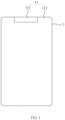
- a display substrate 1 includes a display region 11.
- the display region 11 includes a first display region 111 and a second display region 112.
- a light transmittance of the first display region 111 is higher than that of the second display region 112.
- the display substrate 1 includes: a plurality of first sub-pixels 21 and a plurality of power lines VDD.
- the plurality of first sub-pixels 21 and the plurality of power lines VDD are located in the first display region 111.
- the plurality of first sub-pixels 21 are arranged in an array along a row direction X and a column direction Y
- the first sub-pixel 21 includes a light emitting element and a pixel circuit for driving the light emitting element to emit light.
- a plurality of power lines 22 are connected to one another.
- the plurality of power lines 22 include at least one type of first power lines 221 or second power lines 222.
- the first power lines 221 are configured to be connected to pixel circuits of the first sub-pixels 21 arranged along the row direction X.
- the second power lines 222 are configured to be connected to pixel circuits of the first sub-pixels 21 arranged along the column direction Y A sum of a number of the first power lines 221 and a number of the second power lines 222 is smaller than a sum of a number of rows and a number of columns of the array.
- the plurality of power lines in the first display region 111 include at least one type of the first power lines 221 or the second power lines 222, and the sum of the number of the first power lines 221 and the number of the second power lines 222 is smaller than the sum of the number of rows and the number of columns of the array formed by the first sub-pixels 21, where the first power lines 221 are configured to be connected to the pixel circuits of the first sub-pixels 21 arranged along the row direction X, and the second power lines 222 are configured to be connected to the pixel circuits of the first sub-pixels 21 arranged along the column direction Y Therefore, there is at least one row of first sub-pixels 21 without first power lines 221 nearby, and there is at least one column of first sub-pixels 21 without second power lines 222 nearby, thereby reducing the number and the occupied area of the power lines, and being beneficial to improve the light transmittance of the first display region 111.
- the display substrate provided by embodiments of the present disclosure has been briefly introduced above.
- the display substrate provided by the embodiments of the present disclosure will be described in detail below.
- the display substrate includes a display region.
- the display region includes a first display region 111 and a second display region 112.
- a light transmittance of the first display region 111 is higher than that of the second display region 112.
- the display substrate includes a plurality of first sub-pixels 21 and a plurality of power lines 22.
- the plurality of first sub-pixels 21 and the plurality of power lines 22 are located in the first display region 111.
- the plurality of first sub-pixels 21 are arranged in an array along a row direction X and a column direction Y
- Each first sub-pixel 21 includes a light emitting element and a pixel circuit for driving the light emitting element to emit light.
- the pixel circuit may include transistors, and may further include capacitors.
- the pixel circuit may be a 1T pixel circuit, a 2T1C pixel circuit, a 3T1C pixel circuit, a 4T1C pixel circuit, a 5T1C pixel circuit, or a 7T1C pixel circuit.
- the 7T1C pixel circuit will be taken as an example for illustration.
- the plurality of first sub-pixels 21 are divided into a plurality of sub-pixel groups 31, and each sub-pixel group 31 includes two adjacent first sub-pixels 21 in the row direction X, and two adjacent first sub-pixels 21 in the column direction Y That is, each sub-pixel group 31 includes four first sub-pixels 21.
- each sub-pixel group 31 includes one red sub-pixel 211, two green sub-pixels 212 and one blue sub-pixel 213.
- the red sub-pixel 211 and the blue sub-pixel 213 may be located in the same column, and the two green sub-pixels 212 may be located in the same column, but they are not limited thereto.
- the second display region 112 includes a plurality of second sub-pixels, and the plurality of second sub-pixels are arranged in an array along the row direction X and the column direction Y
- a density of the first sub-pixels 21 in the first display region 111 is smaller than that of the second sub-pixels in the second display region 112.
- the density of the first sub-pixels 21 in the first display region 111 may be 1/2 of that of the second sub-pixels in the second display region 112.
- a distance S1 between two adjacent sub-pixel groups 31 is higher than a width W of the sub-pixel group 31 in the row direction X.
- the distance S1 between two adjacent sub-pixel groups 31 may be equal to the width W of the sub-pixel group 31 in the row direction X. In this way, the light transmittance of the first display region 111 can be improved.
- a distance S2 between two adjacent sub-pixel groups 31 is equal to a length L of the sub-pixel group 31 in the column direction Y
- the distance S2 between two adjacent sub-pixel groups 31 may be higher than the length L of the sub-pixel group 31 in the column direction Y In this way, the light transmittance of the first display region 111 can be improved.
- orthographic projections of sub-pixel groups 31 in an ( i +2) th row on sub-pixel groups 31 in an i th row are located outside orthographic projections of sub-pixel groups 31 in an ( i +1) th row on the sub-pixel groups 31 in the i th row
- orthographic projections of sub-pixel groups 31 in an ( i +3) th row on the sub-pixel groups 31 in the i th row overlaps the orthographic projections of sub-pixel groups 31 in the ( i +1) th row on the sub-pixel groups 31 in the i th row
- the orthographic projections of sub-pixel groups 31 in the ( i +3) th row on the sub-pixel groups 31 in the i th row are located outside the orthographic projections of sub-pixel groups 31 in the ( i +2) th row on the sub-pixel groups 31 in the i th row, where i is a positive integer.
- orthographic projections of sub-pixel groups 31 in a third row on sub-pixel groups 31 in a first row are located outside orthographic projections of sub-pixel groups 31 in a second row on the sub-pixel groups 31 in the first row
- orthographic projections of sub-pixel groups 31 in a fourth row on the sub-pixel groups 31 in the first row overlaps the orthographic projections of sub-pixel groups 31 in the second row on the sub-pixel groups 31 in the first row
- the orthographic projections of sub-pixel groups 31 in the fourth row on the sub-pixel groups 31 in the first row are located outside the orthographic projections of sub-pixel groups 31 in the third row on the sub-pixel groups 31 in the first row.
- orthographic projections of sub-pixel groups 31 in a ( j +2) th column on sub-pixel groups 31 in a j th column are located outside orthographic projections of sub-pixel groups 31 in a ( j +1) th column on the sub-pixel groups 31 in the j th column
- orthographic projections of sub-pixel groups 31 in a ( j +3) th column on the sub-pixel groups 31 in the j th column overlaps the orthographic projections of sub-pixel groups 31 in the ( j +1) th column on the sub-pixel groups 31 in the j th column
- the orthographic projections of sub-pixel groups 31 in the ( j +3) th column on the sub-pixel groups 31 in the j th column are located outside the orthographic projections of sub-pixel groups 31 in the ( j +2) th column on the sub-pixel groups 31 in the j th column, where j is a positive integer.
- orthographic projections of sub-pixel groups 31 in a third column on sub-pixel groups 31 in a first column are located outside orthographic projections of sub-pixel groups 31 in a second column on the sub-pixel groups 31 in the first column
- orthographic projections of sub-pixel groups 31 in a fourth column on the sub-pixel groups 31 in the first column overlaps the orthographic projections of sub-pixel groups 31 in the second column on the sub-pixel groups 31 in the first column
- the orthographic projections of sub-pixel groups 31 in the fourth column on the sub-pixel groups 31 in the first column are located outside the orthographic projections of sub-pixel groups 31 in the third column on the sub-pixel groups 31 in the first column.
- the plurality of power lines 22 are connected to one another. In this way, a resistance of the power lines can be reduced, and further, a voltage drop of power supply voltages in the column direction Y can be decreased.
- the plurality of power lines 22 include first power lines 221, second power lines 222 and third power lines 223.
- the first power lines 221, the second power lines 222 and the third power lines 223 are located in the first display region 111.
- the first power lines 221 are configured to be connected to pixel circuits of the first sub-pixels 21 arranged along the row direction X.
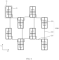
- a number of the first power lines 221 is smaller than a number of rows of the array, the number of the first power lines 221 is equal to 0.25 time the number of rows of the array, and the number of the first power lines 221 is equal to 0.5 time a number of the sub-pixel groups 31.
- FIG 2 8 rows of first sub-pixels 21 and 4 rows of sub-pixel groups 31 are shown, and the number of first power lines 221 is 2.
- pixel circuits of four first sub-pixels 21 in the same sub-pixel group 31 are connected to just the same first power line 221, and the same first power line 221 is connected to pixel circuits of first sub-pixels 21 in sub-pixel groups 31 in two adjacent rows, that is, the same first power line 221 is connected to pixel circuits of first sub-pixels 21 in four adjacent rows.
- the second power lines 222 are configured to be connected to pixel circuits of the first sub-pixels 21 arranged along the column direction Y
- a number of the second power lines 222 is smaller than a number of columns of the array
- the number of the second power lines 222 is equal to 0.5 time the number of columns of the array
- the number of the second power lines 222 is equal to a number of columns of the sub-pixel groups 31.
- 8 columns of first sub-pixels 21 and 4 columns of sub-pixel groups 31 are shown, and the number of second power lines 222 is 4.
- pixel circuits of four first sub-pixels 21 in sub-pixel groups 31 in the same column are connected to the same second power line 222.
- the same second power line 222 is connected to pixel circuits of four first sub-pixels 21 in sub-pixel groups 31 in the same column.
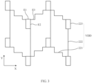
- the third power lines 223 are connected to the first power lines 221 and the second power lines 222, and a number of the third power lines 223 is the same as a number of the sub-pixel groups 31. Pixel circuits of four first sub-pixels 21 in each sub-pixel group 31 are connected to the same third power line 223.
- the third power lines 223 may have a ring shape, for example, a rectangular ring shape, but they are not limited thereto.
- the third power line 223 includes a first conductive portion E1 and a second conductive portion E2.
- the first conductive portion E1 is connected to the second conductive portion E2.
- the first conductive portion E1 extends along the row direction X
- the second conductive portion E2 extends along the column direction Y
- the first power line 221 includes a third conductive portion E3.
- the third conductive portion E3 extends along the row direction X
- the second power line 222 extends along the column direction Y
- the first conductive portion E1 is connected to the third conductive portion E3
- a second power line 222 is connected to the second conductive portion E2.
- the first conductive portion E1 is connected to a second power line 222.
- a sum of the number of the first power lines 221 and the number of the second power lines 222 is smaller than a sum of the number of rows and the number of columns of the array. Therefore, at least one row of first sub-pixels 21 without first power lines 221 nearby, and at least one column of first sub-pixels 21 without second power lines 222 nearby, thereby reducing the number and an occupied area of the power lines, and being beneficial to improve the light transmittance of the first display region 111.
- the plurality of power lines 22 further include fourth power lines and fifth power lines.
- the fourth power lines and the fifth power lines may be located in the second display region 112.
- the first power lines 221, the second power lines 222, the third power lines 223, the fourth power lines, and the fifth power lines are connected to one another.
- the fourth power lines are configured to be connected to pixel circuits of the second sub-pixels arranged along the row direction X, and the fifth power lines are configured to be connected to pixel circuits of the second sub-pixels arranged along the column direction Y
- a number of the fourth power lines is the same as a number of rows of the array. Pixel circuits of second sub-pixels in the same row are connected to the same fourth power line, and the same fourth power line is connected to pixel circuits of second sub-pixels in the same row.
- a number of the fifth source lines is the same as a number of columns of the array. Pixel circuits of second sub-pixels in the same column are connected to the same fifth power line, and the same fifth power line is connected to pixel circuits of second sub-pixels in the same column.
- a density of the power lines in the first display region 111 is smaller than that in the second display region 112. Since the density of the power lines in the first display region 111 is smaller than that in the second display region 112, the light transmittance of the first display region 111 can be improved.
- FIGS. 2-4 A structure of the display substrate in some embodiments has been shown above briefly in FIGS. 2-4 . The structure of the display substrate in some embodiments will be further described below.
- a pixel circuit 51 is connected to a light emitting element D for driving the light emitting element D to emit light.
- the pixel circuit 51 is connected to a power line VDD, and a negative electrode of the light emitting element D is connected to a power line VSS.
- the pixel circuit 51 may include a drive transistor T1, a data writing transistor T2, a threshold compensation transistor T3, a second light emission control transistor T4, a first light emission control transistor T5, a first reset transistor T6, a second reset transistor T7 and a storage capacitor C.
- the threshold compensation transistor T3 and the first reset transistor T6 may be double-gate transistors.
- the drive transistor T1 is used to provide a drive current for the light emitting element D.
- a gate electrode of the drive transistor T1 is connected to a first electrode of the capacitor C, a first electrode of the threshold compensation transistor T3, and a second electrode of the first reset transistor T6.
- a first electrode of the drive transistor T1 is connected to a second electrode of the threshold compensation transistor T3 and a second electrode of the first light emission control transistor T5.
- a second electrode of the drive transistor T1 is connected to a first electrode of the second light emission control transistor T4 and a second electrode of the data writing transistor T2.
- a first electrode of the data writing transistor T2 is configured to be electrically connected to a data line Vd to receive data signals.
- a gate electrode of the data writing transistor T2 is electrically connected to a first scan signal line Ga1 to receive scan signals, and the first electrode of the data writing transistor T2 is electrically connected to the data line Vd to receive the data signals.
- a gate electrode of the threshold compensation transistor T3 is electrically connected to a second scan signal line Ga2 to receive compensation control signals.
- a gate electrode of the second light emission control transistor T4 is electrically connected to a first light emission control signal line EM1 to receive first light emission control signals, and a second electrode of the second light emission control transistor T4 is connected to a second electrode of the capacitor and the power line VDD.
- a gate electrode of the first light emission control transistor T5 is electrically connected to a second light emission control signal line EM2 to receive second light emission control signals, and a first electrode of the first light emission control transistor T5 is connected to a first electrode of the second reset transistor T7 and a positive electrode of the light emitting element D.
- a gate electrode of the first reset transistor T6 is electrically connected to a first reset control signal line Rst1 to receive first sub-reset control signals, and a first electrode of the first reset transistor T6 is electrically connected to a first reset power supply terminal Vinit1 to receive first reset signals.
- a gate electrode of the second reset transistor T7 is electrically connected to a second reset control signal line Rst2 to receive second sub-reset control signals, and a second electrode of the second reset transistor T7 is electrically connected to a second reset power supply terminal Vinit2 to receive second reset signals.
- the drive transistor T1, the data writing transistor T2, the threshold compensation transistor T3, the second light emission control transistor T4, the first light emission control transistor T5, the first reset transistor T6, and the second reset transistor T7 are P transistors, their first electrodes are source electrodes, and their second electrodes are drain electrodes.
- one or more of the drive transistor T1, the data writing transistor T2, the threshold compensation transistor T3, the second light emission control transistor T4, the first light emission control transistor T5, the first reset transistor T6, and the second reset transistor T7 may be N transistors.
- a voltage of power supply signals provided by the power line VDD is higher than that provided by the power line VSS.
- the voltage of the power supply signals provided by the power line VDD is a positive voltage, and the voltage of the power supply signals provided by the power line VSS may be 0 or a negative voltage.
- a voltage of power supply signals provided by the power line VSS when being grounded is 0.
- the voltage of the power supply signals provided by the power line VDD may be smaller than that provided by the power line VSS.
- the first light emission control signals may be the same as the second light emission control signals, and the gate electrode of the second light emission control transistor T4 and the gate electrode of the first light emission control transistor T5 may be connected to the same light emission control signal line EM, where the light emission control signal line EM is the first light emission control signal line EM1 or the second light emission control signal line EM2.
- the first sub-reset control signals may be the same as the second sub-reset control signals, and the gate electrode of the first reset transistor T6 and the gate electrode of the second reset transistor T7 may be connected to the same reset control signal line Rst, where the reset control signal line Rst may be the first reset control signal line Rst1 or the second reset control signal line Rst2.
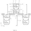
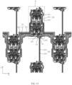
- FIGS. 6 to 14 show structures of layers of pixel circuits of 4 rows and 6 columns of first sub-pixels 21, or structures of layers of pixel circuits of first sub-pixels 21 in 2 rows and 3 columns of sub-pixel groups 31.
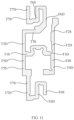
- FIGS. 6 to 11 show structures of an active semiconductor layer 61 in a pixel circuit.
- the active semiconductor layer 61 may be formed by patterning semiconductor material.
- the active semiconductor layer 61 may be used to manufacture active layers of drive transistors T1, data writing transistors T2, threshold compensation transistors T3, second light emission control transistors T4, first light emission control transistors T5, first reset transistors T6, and second reset transistors T7.
- An active semiconductor layer 61 includes active layer patterns and doped region patterns of transistors of the sub-pixels, where a doped region pattern includes a source region and a drain region. Active layer patterns and doped region patterns of transistors in the same pixel circuit are integrally disposed.
- a drive transistor T1 includes an active layer T1C, a source region T1S, and a drain region T1D;
- a data writing transistor T2 includes an active layer T2C, a source region T2S, and a drain region T2D;
- a threshold compensation transistor T3 includes an active layer T3C, a source region T3S, and a drain region T3D;
- a second light emission control transistor T4 includes an active layer T4C, a source region T4S, and a drain region T4D;
- a first light emission control transistor T5 includes an active layer T5C, a source region T5S, and a drain region T5D;
- a first reset transistor T6 includes an active layer T6C, a source region T6S, and a drain region T6D; and
- a second reset transistor T7 includes an active layer T7C, a source region T7S, and a drain region T7D.
- an active layer may include an integrally formed low-temperature polysilicon layer, and a source region and a drain region may be subjected to conductor processing by doping or the like to achieve electrical connection between structures. That is, an active semiconductor layer of transistors of each first sub-pixel 21 is an overall pattern formed of p-silicon, and each transistor in the same pixel circuit includes a doped region pattern (i.e., a source region and a drain region) and an active layer pattern. Active layers of different transistors are separated by doped structures.
- the active semiconductor layers 61 may be made of amorphous silicon, polysilicon, oxide semiconductor materials, or the like. It will be noted that the source regions and the drain regions may be regions doped with N or P impurities.
- each sub-pixel group 31 active semiconductor layers 61 are symmetrical about a symmetry axis 71, and the symmetry axis 71 extends along a column direction Y, that is, active semiconductor layers 61 of pixel circuits of a red sub-pixel 211 and a green sub-pixel 212 located in the same row are symmetrical about the symmetry axis 71, and active semiconductor layers 61 of pixel circuits of a blue sub-pixel 213 and a green sub-pixel 212 located in the same row are symmetrical about the symmetry axis 71. It will be noted that each sub-pixel group 31 is also symmetrical about the symmetry axis 71.
- FIGS. 8 to 11 show a structure of an active semiconductor layer 61 of a pixel circuit of a red sub-pixel 211.
- FIGS. 10 and 11 show a structure of an active semiconductor layer 61 of a pixel circuit of a blue sub-pixel 213.
- FIG 12 shows a structure of a first conductive layer 121 in a pixel circuit.
- the first conductive layer 121 is located on a gate insulation layer.
- the first conductive layer 121 is located on the gate insulation layer and insulated from an active semiconductor layer 61.
- the first conductive layer 121 may include a first electrode CC1 of a storage capacitor C, a first scan signal line Ga1, a reset control signal line Rst, a light emission control signal line EM, and a first vertical conductive portion 2221, and the first conductive layer 121 may include gate electrodes of a drive transistor T1, a data writing transistor T2, a threshold compensation transistor T3, a second light emission control transistor T4, a first light emission control transistor T5, a first reset transistor T6, and a second reset transistor T7.
- the first electrode CC1 of the storage capacitor C is also the gate electrode of the drive transistor T 1.
- the gate electrode of the data writing transistor T2 may be a portion where the first scan signal line Ga1 overlaps the active semiconductor layer 61;
- the gate electrode of the second light emission control transistor T4 may be a first portion where the light emission control signal line EM overlaps the active semiconductor layer 61, and the gate electrode of the first light emission control transistor T5 may be a second portion where the light emission control signal line EM overlaps the active semiconductor layer 61;
- the gate electrode of the first reset transistor T6 is a first portion where the reset control signal line Rst overlaps the active semiconductor layer 61, and the gate electrode of the second reset transistor T7 is a second portion where the reset control signal line Rst overlaps the active semiconductor layer 61;
- the threshold compensation transistor T3 may be a thin film transistor with a double-gate structure, a first gate electrode of the threshold compensation transistor T3 may be a portion where the first scan signal line Ga1 overlaps the active semiconductor layer 61, and a second gate electrode of the threshold compensation transistor T3 may be a portion where a protru
- the first vertical conductive portion 2221 extends along a column direction Y, and constitutes a part of a second power line 222.
- the first vertical conductive portion 2221 includes connecting portions 122 for connecting with other portions of power lines through via holes.
- FIG 13 shows a structure of a second conductive layer 131 in a pixel circuit.
- the second conductive layer 131 includes a reset signal line VINIT, a second electrode CC2 of a storage capacitor C, a second vertical conductive portion 2222, a first horizontal conductive portion 2211, a second horizontal conductive portion 2212, and a light shielding portion SHL.
- Reset signal lines VINIT of pixel circuits of all first sub-pixels 21 are connected together.
- the second electrode CC2 is connected to a power line, for example, a second electrode CC2 in a red sub-pixel 211 may be a part of a first conductive portion E1 of a third power line 223, a second electrode CC2 in a blue sub-pixel 213 is a part of another first conductive portion E1 of the third power line 223, the second electrode CC2 in the blue sub-pixel 213 is also connected to the second horizontal conductive portion 2212, the second horizontal conductive portion 2212 and the first horizontal conductive portion 2211 are parts of a first power line 221, and the second vertical conductive portion 2222 is a part of a second power line 222.
- the light shielding portion SHL is used for shielding light to prevent a double-gate transistor from being optically disturbed.
- the light shielding portion SHL may be connected to a DC power supply, so that the light shielding portion SHL can play an electrical shielding role to prevent the double-gate transistor from being electrically disturbed.
- a horizontal conductive portion does not refer to that the conductive portion extends along a row direction X, but is used to be connected with pixel circuits of first sub-pixels 21 arranged along the row direction X.
- a vertical conductive portion may refer to that the conductive portion extends along a column direction Y
- the second vertical conductive portion 2222 includes connecting portions 132 for connecting with other portions of power lines through via holes.
- the first horizontal conductive portion 2211 includes a connecting portion 133 for connecting with the second horizontal conductive portion 2212 through a via hole
- the second horizontal conductive portion 2212 includes a connecting portion 134 for connecting with the first horizontal conductive portion 2211 through a via hole.
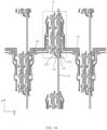
- FIG. 14 shows a structure of a third conductive layer 141 in a pixel circuit.
- the third conductive layer 141 includes a data line Vd, a third vertical conductive portion 2231, a fourth vertical conductive portion 2232, and connecting portions 142.
- the third vertical conductive portion 2231 and the fourth vertical conductive portion 2232 extend along a column direction Y respectively.
- the third vertical conductive portion 2231 and the fourth vertical conductive portion 2232 are second conductive portions E2.
- the third vertical conductive portion 2231 and the fourth vertical conductive portion 2232 are respectively connected to a second electrode CC2 through via holes to realize a ring-shaped structure of a third power line 223.
- the third vertical conductive portion 2231 includes a connecting portion 143, where the connecting portion 143 is connected to a connecting portion 132 of the second vertical conductive portion 2222 through a via hole
- the fourth vertical conductive portion 2232 includes a connecting portion 144, where the connecting portion 144 is connected to a connecting portion 122 of the first vertical conductive portion 2221 through a via hole, so as to realize the connection between a third power line 223 and a second power line 222.
- the connecting portions 142 are respectively connected to a connecting portion 133 of the first horizontal conductive portion 2211 and a connecting portion 134 of the second horizontal conductive portion 2212 through via holes to form a first power line 221.
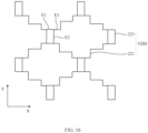
- a plurality of power lines 22 include only first power lines 221 and third power lines 223, but do not include second power lines 222, that is, a number of the second power lines 222 is 0, and a density of the first power lines 221 is higher than that in the above embodiments.
- a first power line 221 exists between pixel circuits of first sub-pixels 21 in sub-pixel groups 31 in two adjacent rows, and the pixel circuits of the first sub-pixels 21 in the sub-pixel groups 31 in two adjacent rows are connected to the same first power line 221, that is, pixel circuits of first sub-pixels 21 in four adjacent rows are connected to the same first power line 221. Also, pixel circuits of first sub-pixels 21 in the same sub-pixel group 31 are connected to two adjacent first power lines 221.
- each third power line 223 includes two first conductive portions E1, and the first conductive portions E1 extend along a row direction X.
- Each first power line 221 includes third conductive portions E3, and the third conductive portions E3 extend along the row direction X.
- First conductive portions of third power lines 223 are connected to third conductive portions of first power lines 221.
- a third power line 223 is respectively connected to two first power lines 221 through two first conductive portions.
- a density of power lines in a first display region 111 is smaller than that in a second display region 112. Since the density of the power lines in the first display region 111 is smaller than that in the second display region 112, a light transmittance of the first display region 111 can be improved.
- each sub-pixel group 31 includes three adjacent first sub-pixels 21 in a row direction X.
- each sub-pixel group 31 includes adjacent red sub-pixel 211, green sub-pixel 212 and blue sub-pixel 213 in the row direction X.
- a density of first sub-pixels 21 in a first display region 111 is smaller than that of second sub-pixels in a second display region 112. In this way, a light transmittance of the first display region 111 can be improved.
- a number of first power lines 221 is equal to a number of rows of the array. Pixel circuits of first sub-pixels 21 in sub-pixel groups 31 in the same row are connected to just the same first power line 221, and the same first power line 221 is connected to just pixel circuits of first sub-pixels 21 in sub-pixel groups 31 in the same row.
- a number of second power lines 222 is smaller than a number of columns of the array. In this way, the number of second power lines 222 can be reduced, and the light transmittance of the first display region 111 can be improved.
- the number of second power lines 222 is equal to 1/3 times a number of columns of the array, and the number of second power lines 222 is equal to a number of columns of sub-pixel groups 31.
- FIG 20 shows 9 columns of first sub-pixels 21, 3 columns of sub-pixel groups 31, and the number of second power lines 222 is equal to 3.
- pixel circuits of first sub-pixels 21 in sub-pixel groups 31 in the same column are connected to the same second power line 222, and the same second power line 222 is connected to pixel circuits of first sub-pixels 21 in sub-pixel groups 31 in the same column.
- Some embodiments of the present disclosure provide a display device, which includes photosensitive elements, and further includes a display substrate according to any of the above embodiments. Projections of the photosensitive elements on the display substrate are located within a first display region 111.
- the photosensitive elements may be image sensors, ambient light sensors or distance sensors, but they are not limited thereto.
- the display device in this embodiment may be any product or component having a display function, such as electronic paper, a mobile phone, a tablet computer, a television, a notebook computer, a digital photo frame, or a navigator.
- a display function such as electronic paper, a mobile phone, a tablet computer, a television, a notebook computer, a digital photo frame, or a navigator.
Landscapes
- Engineering & Computer Science (AREA)
- Microelectronics & Electronic Packaging (AREA)
- Physics & Mathematics (AREA)
- Computer Hardware Design (AREA)
- General Physics & Mathematics (AREA)
- Theoretical Computer Science (AREA)
- Electroluminescent Light Sources (AREA)
- Devices For Indicating Variable Information By Combining Individual Elements (AREA)
Abstract
Description
- The present application relates to the field of display technologies, and in particular, to display substrates and display devices.
- In the related art, organic light emitting diode (OLED) display substrates have a wide range of applications in fields of smart phones, televisions, virtual reality (VR ) devices, wearable devices, etc. due to their excellent display effect, and characteristics such as thinness, flexibility, excellent shock resistance, and suitability for wearable products. As requirements on screen-to-body ratios of display substrates of terminal devices with cameras, such as mobile phones, is getting higher and higher, disposing the cameras under the display substrates is one of the best solutions to meet such requirements. However, disposing the cameras under the display substrates places higher requirements on the performance of the display substrates, especially on their light transmittance. High light transmittance of regions for enabling the cameras to capture images on the display substrates is a basic condition for applying this solution. Therefore, how to improve the light transmittance of the display substrates is a technical problem that needs to be solved.
- The present disclosure provides display substrates and display devices.
- According to a first aspect of embodiments of the present disclosure, there is provided a display substrate, including: a display region including a first display region and a second display region, where a light transmittance of the first display region is higher than that of the second display region; the display substrate further including: a plurality of first sub-pixels and a plurality of power lines, where
the plurality of first sub-pixels and the plurality of power lines are located in the first display region; the plurality of first sub-pixels are arranged in an array along a row direction and a column direction; a first sub-pixel includes a light emitting element and a pixel circuit for driving the light emitting element to emit light; the plurality of power lines are connected to one another; the plurality of power lines include at least one type of first power lines or second power lines, the first power lines are configured to be connected to pixel circuits of the first sub-pixels arranged in the row direction, and the second power lines are configured to be connected to pixel circuits of the first sub-pixels arranged in the column direction; a sum of a number of the first power lines and a number of the second power lines is smaller than a sum of a number of rows and a number of columns of the array. - In some embodiments, the plurality of first sub-pixels are divided into a plurality of sub-pixel groups, and each sub-pixel group includes at least one of: at least two adjacent first sub-pixels in the row direction or at least two adjacent first sub-pixels in the column direction.
- In some embodiments, each sub-pixel group includes two adjacent first sub-pixels in the row direction and two adjacent first sub-pixels in the column direction.
- In some embodiments, in a same row of sub-pixel groups, a distance between two adjacent sub-pixel groups is higher than or equal to a width of the sub-pixel group in the row direction;
in a same column of sub-pixel groups, a distance between two adjacent sub-pixel groups is higher than or equal to a length of the sub-pixel group in the column direction. - In some embodiments, orthographic projections of sub-pixel groups in an (i+2)th row on sub-pixel groups in an i th row are located outside orthographic projections of sub-pixel groups in an (i+1)th row on the sub-pixel groups in the i th row, orthographic projections of sub-pixel groups in an (i+3)th row on the sub-pixel groups in the i th row overlaps the orthographic projections of sub-pixel groups in the (i+1)th row on the sub-pixel groups in the i th row, and the orthographic projections of sub-pixel groups in the (i+3)th row on the sub-pixel groups in the i th row are located outside the orthographic projections of sub-pixel groups in the (i+2)th row on the sub-pixel groups in the i th row, where i is a positive integer;
- orthographic projections of sub-pixel groups in a (j+2)th column on sub-pixel groups in a j th column are located outside orthographic projections of sub-pixel groups in a (j+1)th column on the sub-pixel groups in the j th column, orthographic projections of sub-pixel groups in a (j+3)th column on the sub-pixel groups in the j th column overlaps the orthographic projections of sub-pixel groups in the (j+1)th column on the sub-pixel groups in the j th column, and the orthographic projections of sub-pixel groups in the (j+3)th column on the sub-pixel groups in the j th column are located outside the orthographic projections of sub-pixel groups in the (j+2)th column on the sub-pixel groups in the j th column, where j is a positive integer.
- In some embodiments, the number of the first power lines is smaller than the number of rows of the array.
- In some embodiments, the number of the first power lines is equal to 0.25 time the number of rows of the array, pixel circuits of first sub-pixels in a same sub-pixel group are connected to just a same first power line, and the same first power line is connected to pixel circuits of first sub-pixels in sub-pixel groups in two adjacent rows.
- In some embodiments, the number of the second power lines is smaller than the number of columns of the array.
- In some embodiments, the number of the second power lines is equal to 0.5 time the number of columns of the array, and the number of the second power lines is equal to a number of columns of the sub-pixel groups;
pixel circuits of first sub-pixels in sub-pixel groups in a same column are connected to a same second power line. - In some embodiments, a first power line exists between pixel circuits of first sub-pixels in sub-pixel groups in two adjacent rows, and the pixel circuits of the first sub-pixels in the sub-pixel groups in two adjacent rows are connected to a same first power line; pixel circuits of first sub-pixels in a same sub-pixel group are connected to two adjacent first power lines.
- In some embodiments, the number of the second power lines is 0.
- In some embodiments, the plurality of power lines further include third power lines, and the third power lines are connected to at least one type of the first power lines or the second power lines;
a number of the third power lines is the same as a number of the sub-pixel groups, and pixel circuits of first sub-pixels in each sub-pixel group are connected to a same third power line. - In some embodiments, the third power lines have a ring shape.
- In some embodiments, when the third power lines are connected to the first power lines and the second power lines, the third power lines include first conductive portions and second conductive portions, the first conductive portions are connected to the second conductive portions, the first conductive portions extend along the row direction, and the second conductive portions extend along the column direction; the first power lines include third conductive portions, and the third conductive portions extend along the row direction; the second power lines extend along the column direction; the first conductive portions are connected to the third conductive portions, and the second power lines are connected to the first conductive portions or the second conductive portions;
when the third power lines are connected to the first power lines, the third power lines include first conductive portions, and the first conductive portions extend along the row direction; the first power lines include third conductive portions, and the third conductive portions extend along the row direction; the first conductive portions are connected to the third conductive portions. - In some embodiments, each sub-pixel group includes three adjacent first sub-pixels in the row direction.
- In some embodiments, the number of the first power lines is equal to the number of rows of the array;
pixel circuits of first sub-pixels in sub-pixel groups in a same row are connected to just a same first power line, and the same first power line is connected to just pixel circuits of first sub-pixels in sub-pixel groups in a same row. - In some embodiments, the number of the second power lines is smaller than the number of columns of the array.
- In some embodiments, the number of the second power lines is equal to 1/3 times the number of columns of the array, and the number of the second power lines is equal to a number of columns of the sub-pixel groups;
pixel circuits of first sub-pixels in sub-pixel groups in a same column are connected to a same second power line, and the same second power line is connected to pixel circuits of first sub-pixels in sub-pixel groups in a same column. - In some embodiments, the second display region includes a plurality of second sub-pixels, and the plurality of second sub-pixels are arranged in an array along the row direction and the column direction;
a density of the first sub-pixels in the first display region is smaller than that of the second sub-pixels in the second display region. - In some embodiments, the plurality of power lines further include fourth power lines and fifth power lines, the fourth power lines are configured to be connected to pixel circuits of the second sub-pixels arranged along the row direction, and the fifth power lines are configured to be connected to pixel circuits of the second sub-pixels arranged along the column direction;
a density of the power lines in the first display region is smaller than that in the second display region. - According to a second aspect of the embodiments of the present disclosure, there is provided a display device, including the above-described display substrate and photosensitive elements, where projections of the photosensitive elements on the display substrate are located within a first display region.
-
-
FIG 1 is a schematic structural diagram illustrating a display substrate according to some embodiments of the present disclosure; -
FIG 2 is a schematic structural diagram illustrating another display substrate according to some embodiments of the present disclosure; -
FIG 3 is a schematic structural diagram illustrating another display substrate according to some embodiments of the present disclosure; -
FIG 4 is a schematic structural diagram illustrating another display substrate according to some embodiments of the present disclosure; -
FIG 5 is a schematic structural diagram illustrating an equivalent circuit of a pixel circuit according to some embodiments of the present disclosure; -
FIGS. 6 to 14 are schematic structural diagrams illustrating layers of a pixel circuit according to some embodiments of the present disclosure; -
FIG 15 is a schematic structural diagram illustrating power lines according to some embodiments of the present disclosure; -
FIG 16 is a schematic structural diagram illustrating another display substrate according to some embodiments of the present disclosure; -
FIG 17 is a schematic structural diagram illustrating another display substrate according to some embodiments of the present disclosure; -
FIG. 18 is a schematic structural diagram illustrating another display substrate according to some embodiments of the present disclosure; -
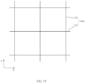
FIG 19 is a schematic structural diagram illustrating another display substrate according to some embodiments of the present disclosure; -
FIG. 20 is a schematic structural diagram illustrating another display substrate according to some embodiments of the present disclosure. - In order to make the above objectives, features and advantages of the present disclosure more clearly understood, specific examples of the present disclosure will be described in detail below with reference to the accompanying drawings.
- Some embodiments of the present disclosure provide a display substrate. A
display substrate 1, as shown inFIG 1 , includes adisplay region 11. Thedisplay region 11 includes afirst display region 111 and asecond display region 112. A light transmittance of thefirst display region 111 is higher than that of thesecond display region 112. - In some embodiments, as shown in
FIGS. 2 to 12 , thedisplay substrate 1 includes: a plurality offirst sub-pixels 21 and a plurality of power lines VDD. - In some embodiments, the plurality of
first sub-pixels 21 and the plurality of power lines VDD are located in thefirst display region 111. The plurality offirst sub-pixels 21 are arranged in an array along a row direction X and a column direction Y Thefirst sub-pixel 21 includes a light emitting element and a pixel circuit for driving the light emitting element to emit light. A plurality of power lines 22 are connected to one another. The plurality of power lines 22 include at least one type offirst power lines 221 orsecond power lines 222. Thefirst power lines 221 are configured to be connected to pixel circuits of the first sub-pixels 21 arranged along the row direction X. Thesecond power lines 222 are configured to be connected to pixel circuits of the first sub-pixels 21 arranged along the column direction Y A sum of a number of thefirst power lines 221 and a number of thesecond power lines 222 is smaller than a sum of a number of rows and a number of columns of the array. - In some embodiments, the plurality of power lines in the
first display region 111 include at least one type of thefirst power lines 221 or thesecond power lines 222, and the sum of the number of thefirst power lines 221 and the number of thesecond power lines 222 is smaller than the sum of the number of rows and the number of columns of the array formed by the first sub-pixels 21, where thefirst power lines 221 are configured to be connected to the pixel circuits of the first sub-pixels 21 arranged along the row direction X, and thesecond power lines 222 are configured to be connected to the pixel circuits of the first sub-pixels 21 arranged along the column direction Y Therefore, there is at least one row of first sub-pixels 21 withoutfirst power lines 221 nearby, and there is at least one column of first sub-pixels 21 withoutsecond power lines 222 nearby, thereby reducing the number and the occupied area of the power lines, and being beneficial to improve the light transmittance of thefirst display region 111. - The display substrate provided by embodiments of the present disclosure has been briefly introduced above. The display substrate provided by the embodiments of the present disclosure will be described in detail below.
- Some embodiments of the present disclosure provide a display substrate. As shown in
FIG 1 , the display substrate includes a display region. The display region includes afirst display region 111 and asecond display region 112. A light transmittance of thefirst display region 111 is higher than that of thesecond display region 112. - In some embodiments, as shown in
FIGS. 2 to 4 , the display substrate includes a plurality of first sub-pixels 21 and a plurality of power lines 22. The plurality of first sub-pixels 21 and the plurality of power lines 22 are located in thefirst display region 111. - In some embodiments, as shown in
FIGS. 2 and4 , the plurality of first sub-pixels 21 are arranged in an array along a row direction X and a column direction Y Eachfirst sub-pixel 21 includes a light emitting element and a pixel circuit for driving the light emitting element to emit light. The pixel circuit may include transistors, and may further include capacitors. The pixel circuit may be a 1T pixel circuit, a 2T1C pixel circuit, a 3T1C pixel circuit, a 4T1C pixel circuit, a 5T1C pixel circuit, or a 7T1C pixel circuit. In this example, the 7T1C pixel circuit will be taken as an example for illustration. - In some embodiments, as shown in
FIGS. 2 and4 , the plurality of first sub-pixels 21 are divided into a plurality ofsub-pixel groups 31, and eachsub-pixel group 31 includes two adjacent first sub-pixels 21 in the row direction X, and two adjacent first sub-pixels 21 in the column direction Y That is, eachsub-pixel group 31 includes fourfirst sub-pixels 21. - In some embodiments, as shown in
FIG 2 , eachsub-pixel group 31 includes onered sub-pixel 211, twogreen sub-pixels 212 and oneblue sub-pixel 213. In eachsub-pixel group 31, thered sub-pixel 211 and theblue sub-pixel 213 may be located in the same column, and the twogreen sub-pixels 212 may be located in the same column, but they are not limited thereto. - In some embodiments, the
second display region 112 includes a plurality of second sub-pixels, and the plurality of second sub-pixels are arranged in an array along the row direction X and the column direction Y A density of the first sub-pixels 21 in thefirst display region 111 is smaller than that of the second sub-pixels in thesecond display region 112. For example, the density of the first sub-pixels 21 in thefirst display region 111 may be 1/2 of that of the second sub-pixels in thesecond display region 112. - In some embodiments, as shown in
FIG 2 , in the same row ofsub-pixel groups 31, a distance S1 between twoadjacent sub-pixel groups 31 is higher than a width W of thesub-pixel group 31 in the row direction X. However, in other embodiments, in the same row ofsub-pixel groups 31, the distance S1 between twoadjacent sub-pixel groups 31 may be equal to the width W of thesub-pixel group 31 in the row direction X. In this way, the light transmittance of thefirst display region 111 can be improved. - In some embodiments, as shown in
FIG 2 , in the same column ofsub-pixel groups 31, a distance S2 between twoadjacent sub-pixel groups 31 is equal to a length L of thesub-pixel group 31 in the column direction Y In other embodiments, in the same column ofsub-pixel groups 31, the distance S2 between twoadjacent sub-pixel groups 31 may be higher than the length L of thesub-pixel group 31 in the column direction Y In this way, the light transmittance of thefirst display region 111 can be improved. - In some embodiments, as shown in
FIGS. 2 and4 , orthographic projections ofsub-pixel groups 31 in an (i+2)th row onsub-pixel groups 31 in an i th row are located outside orthographic projections ofsub-pixel groups 31 in an (i+1)th row on thesub-pixel groups 31 in the i th row, orthographic projections ofsub-pixel groups 31 in an (i+3)th row on thesub-pixel groups 31 in the i th row overlaps the orthographic projections ofsub-pixel groups 31 in the (i+1)th row on thesub-pixel groups 31 in the i th row, and the orthographic projections ofsub-pixel groups 31 in the (i+3)th row on thesub-pixel groups 31 in the i th row are located outside the orthographic projections ofsub-pixel groups 31 in the (i+2)th row on thesub-pixel groups 31 in the i th row, where i is a positive integer. - For example, when i is 1, orthographic projections of
sub-pixel groups 31 in a third row onsub-pixel groups 31 in a first row are located outside orthographic projections ofsub-pixel groups 31 in a second row on thesub-pixel groups 31 in the first row, orthographic projections ofsub-pixel groups 31 in a fourth row on thesub-pixel groups 31 in the first row overlaps the orthographic projections ofsub-pixel groups 31 in the second row on thesub-pixel groups 31 in the first row, and the orthographic projections ofsub-pixel groups 31 in the fourth row on thesub-pixel groups 31 in the first row are located outside the orthographic projections ofsub-pixel groups 31 in the third row on thesub-pixel groups 31 in the first row. - In some embodiments, as shown in
FIGS. 2 and4 , orthographic projections ofsub-pixel groups 31 in a (j+2)th column onsub-pixel groups 31 in a j th column are located outside orthographic projections ofsub-pixel groups 31 in a (j+1)th column on thesub-pixel groups 31 in the j th column, orthographic projections ofsub-pixel groups 31 in a (j+3)th column on thesub-pixel groups 31 in the j th column overlaps the orthographic projections ofsub-pixel groups 31 in the (j+1)th column on thesub-pixel groups 31 in the j th column, and the orthographic projections ofsub-pixel groups 31 in the (j+3)th column on thesub-pixel groups 31 in the j th column are located outside the orthographic projections ofsub-pixel groups 31 in the (j+2)th column on thesub-pixel groups 31 in the j th column, where j is a positive integer. - For example, when j is 1, orthographic projections of
sub-pixel groups 31 in a third column onsub-pixel groups 31 in a first column are located outside orthographic projections ofsub-pixel groups 31 in a second column on thesub-pixel groups 31 in the first column, orthographic projections ofsub-pixel groups 31 in a fourth column on thesub-pixel groups 31 in the first column overlaps the orthographic projections ofsub-pixel groups 31 in the second column on thesub-pixel groups 31 in the first column, and the orthographic projections ofsub-pixel groups 31 in the fourth column on thesub-pixel groups 31 in the first column are located outside the orthographic projections ofsub-pixel groups 31 in the third column on thesub-pixel groups 31 in the first column. - In some embodiments, as shown in
FIGS. 3 and4 , the plurality of power lines 22 are connected to one another. In this way, a resistance of the power lines can be reduced, and further, a voltage drop of power supply voltages in the column direction Y can be decreased. - In some embodiments, as shown in
FIGS. 3 and4 , the plurality of power lines 22 includefirst power lines 221,second power lines 222 andthird power lines 223. Thefirst power lines 221, thesecond power lines 222 and thethird power lines 223 are located in thefirst display region 111. - In some embodiments, as shown in
FIGS. 3 and4 , thefirst power lines 221 are configured to be connected to pixel circuits of the first sub-pixels 21 arranged along the row direction X. In some embodiments, a number of thefirst power lines 221 is smaller than a number of rows of the array, the number of thefirst power lines 221 is equal to 0.25 time the number of rows of the array, and the number of thefirst power lines 221 is equal to 0.5 time a number of thesub-pixel groups 31. For example, inFIG 2 ,8 rows of first sub-pixels 21 and 4 rows ofsub-pixel groups 31 are shown, and the number offirst power lines 221 is 2. - In some embodiments, as shown in
FIG. 4 , pixel circuits of four first sub-pixels 21 in the same sub-pixel group 31are connected to just the samefirst power line 221, and the samefirst power line 221 is connected to pixel circuits of first sub-pixels 21 insub-pixel groups 31 in two adjacent rows, that is, the samefirst power line 221 is connected to pixel circuits of first sub-pixels 21 in four adjacent rows. - In some embodiments, as shown in
FIG 4 , thesecond power lines 222 are configured to be connected to pixel circuits of the first sub-pixels 21 arranged along the column direction Y In some embodiments, a number of thesecond power lines 222 is smaller than a number of columns of the array, the number of thesecond power lines 222 is equal to 0.5 time the number of columns of the array, and the number of thesecond power lines 222 is equal to a number of columns of thesub-pixel groups 31. For example, inFIG. 4 ,8 columns of first sub-pixels 21 and 4 columns ofsub-pixel groups 31 are shown, and the number ofsecond power lines 222 is 4. - In some embodiments, as shown in
FIGS. 3 and4 , pixel circuits of four first sub-pixels 21 insub-pixel groups 31 in the same column are connected to the samesecond power line 222. The samesecond power line 222 is connected to pixel circuits of four first sub-pixels 21 insub-pixel groups 31 in the same column. - In some embodiments, as shown in
FIGS. 3 and4 , thethird power lines 223 are connected to thefirst power lines 221 and thesecond power lines 222, and a number of thethird power lines 223 is the same as a number of thesub-pixel groups 31. Pixel circuits of four first sub-pixels 21 in eachsub-pixel group 31 are connected to the samethird power line 223. Thethird power lines 223 may have a ring shape, for example, a rectangular ring shape, but they are not limited thereto. - In some embodiments, as shown in
FIG 3 , thethird power line 223 includes a first conductive portion E1 and a second conductive portion E2. The first conductive portion E1 is connected to the second conductive portion E2. The first conductive portion E1 extends along the row direction X, and the second conductive portion E2 extends along the column direction Y - In some embodiments, as shown in
FIG. 3 , thefirst power line 221 includes a third conductive portion E3. The third conductive portion E3 extends along the row direction X, and thesecond power line 222 extends along the column direction Y For somethird power lines 223, for example, the secondthird power line 223 from the left inFIG 3 , the first conductive portion E1 is connected to the third conductive portion E3, and asecond power line 222 is connected to the second conductive portion E2. For some otherthird power lines 223, for example, thethird power line 223 on the rightmost inFIG 3 , the first conductive portion E1 is connected to asecond power line 222. - In some embodiments, a sum of the number of the
first power lines 221 and the number of thesecond power lines 222 is smaller than a sum of the number of rows and the number of columns of the array. Therefore, at least one row of first sub-pixels 21 withoutfirst power lines 221 nearby, and at least one column of first sub-pixels 21 withoutsecond power lines 222 nearby, thereby reducing the number and an occupied area of the power lines, and being beneficial to improve the light transmittance of thefirst display region 111. - In some embodiments, the plurality of power lines 22 further include fourth power lines and fifth power lines. The fourth power lines and the fifth power lines may be located in the
second display region 112. Thefirst power lines 221, thesecond power lines 222, thethird power lines 223, the fourth power lines, and the fifth power lines are connected to one another. - In some embodiments the fourth power lines are configured to be connected to pixel circuits of the second sub-pixels arranged along the row direction X, and the fifth power lines are configured to be connected to pixel circuits of the second sub-pixels arranged along the column direction Y
- In some embodiments, in the second display region, a number of the fourth power lines is the same as a number of rows of the array. Pixel circuits of second sub-pixels in the same row are connected to the same fourth power line, and the same fourth power line is connected to pixel circuits of second sub-pixels in the same row.
- In some embodiments, in the second display region, a number of the fifth source lines is the same as a number of columns of the array. Pixel circuits of second sub-pixels in the same column are connected to the same fifth power line, and the same fifth power line is connected to pixel circuits of second sub-pixels in the same column.
- In some embodiments, a density of the power lines in the
first display region 111 is smaller than that in thesecond display region 112. Since the density of the power lines in thefirst display region 111 is smaller than that in thesecond display region 112, the light transmittance of thefirst display region 111 can be improved. - A structure of the display substrate in some embodiments has been shown above briefly in
FIGS. 2-4 . The structure of the display substrate in some embodiments will be further described below. - A structure of a pixel circuit will be first introduced. As shown in
FIG 5 , apixel circuit 51 is connected to a light emitting element D for driving the light emitting element D to emit light. Thepixel circuit 51 is connected to a power line VDD, and a negative electrode of the light emitting element D is connected to a power line VSS. - As shown in
FIG 5 , thepixel circuit 51 may include a drive transistor T1, a data writing transistor T2, a threshold compensation transistor T3, a second light emission control transistor T4, a first light emission control transistor T5, a first reset transistor T6, a second reset transistor T7 and a storage capacitor C. The threshold compensation transistor T3 and the first reset transistor T6 may be double-gate transistors. - In some embodiments, the drive transistor T1 is used to provide a drive current for the light emitting element D. A gate electrode of the drive transistor T1 is connected to a first electrode of the capacitor C, a first electrode of the threshold compensation transistor T3, and a second electrode of the first reset transistor T6. A first electrode of the drive transistor T1 is connected to a second electrode of the threshold compensation transistor T3 and a second electrode of the first light emission control transistor T5. A second electrode of the drive transistor T1 is connected to a first electrode of the second light emission control transistor T4 and a second electrode of the data writing transistor T2. A first electrode of the data writing transistor T2 is configured to be electrically connected to a data line Vd to receive data signals. A gate electrode of the data writing transistor T2 is electrically connected to a first scan signal line Ga1 to receive scan signals, and the first electrode of the data writing transistor T2 is electrically connected to the data line Vd to receive the data signals. A gate electrode of the threshold compensation transistor T3 is electrically connected to a second scan signal line Ga2 to receive compensation control signals. A gate electrode of the second light emission control transistor T4 is electrically connected to a first light emission control signal line EM1 to receive first light emission control signals, and a second electrode of the second light emission control transistor T4 is connected to a second electrode of the capacitor and the power line VDD. A gate electrode of the first light emission control transistor T5 is electrically connected to a second light emission control signal line EM2 to receive second light emission control signals, and a first electrode of the first light emission control transistor T5 is connected to a first electrode of the second reset transistor T7 and a positive electrode of the light emitting element D. A gate electrode of the first reset transistor T6 is electrically connected to a first reset control signal line Rst1 to receive first sub-reset control signals, and a first electrode of the first reset transistor T6 is electrically connected to a first reset power supply terminal Vinit1 to receive first reset signals. A gate electrode of the second reset transistor T7 is electrically connected to a second reset control signal line Rst2 to receive second sub-reset control signals, and a second electrode of the second reset transistor T7 is electrically connected to a second reset power supply terminal Vinit2 to receive second reset signals.
- In some embodiments, the drive transistor T1, the data writing transistor T2, the threshold compensation transistor T3, the second light emission control transistor T4, the first light emission control transistor T5, the first reset transistor T6, and the second reset transistor T7 are P transistors, their first electrodes are source electrodes, and their second electrodes are drain electrodes. In other embodiments, one or more of the drive transistor T1, the data writing transistor T2, the threshold compensation transistor T3, the second light emission control transistor T4, the first light emission control transistor T5, the first reset transistor T6, and the second reset transistor T7 may be N transistors.
- In some embodiments, a voltage of power supply signals provided by the power line VDD is higher than that provided by the power line VSS. The voltage of the power supply signals provided by the power line VDD is a positive voltage, and the voltage of the power supply signals provided by the power line VSS may be 0 or a negative voltage. For example, a voltage of power supply signals provided by the power line VSS when being grounded is 0. However, in other embodiments, the voltage of the power supply signals provided by the power line VDD may be smaller than that provided by the power line VSS.
- In some embodiments, the first light emission control signals may be the same as the second light emission control signals, and the gate electrode of the second light emission control transistor T4 and the gate electrode of the first light emission control transistor T5 may be connected to the same light emission control signal line EM, where the light emission control signal line EM is the first light emission control signal line EM1 or the second light emission control signal line EM2. Similarly, the first sub-reset control signals may be the same as the second sub-reset control signals, and the gate electrode of the first reset transistor T6 and the gate electrode of the second reset transistor T7 may be connected to the same reset control signal line Rst, where the reset control signal line Rst may be the first reset control signal line Rst1 or the second reset control signal line Rst2. When the first reset signals are the same as the second reset signals, the first reset power supply terminal Vinit1 and the second reset power supply terminal Vinit2 are connected to the same reset signal line VINIT.
- The structure of a pixel circuit has been described above. Structures of layers of pixel circuits will be described below with reference to
FIGS. 6 to 14. FIGS. 6 to 14 show structures of layers of pixel circuits of 4 rows and 6 columns of first sub-pixels 21, or structures of layers of pixel circuits of first sub-pixels 21 in 2 rows and 3 columns ofsub-pixel groups 31. -
FIGS. 6 to 11 show structures of anactive semiconductor layer 61 in a pixel circuit. Theactive semiconductor layer 61 may be formed by patterning semiconductor material. Theactive semiconductor layer 61 may be used to manufacture active layers of drive transistors T1, data writing transistors T2, threshold compensation transistors T3, second light emission control transistors T4, first light emission control transistors T5, first reset transistors T6, and second reset transistors T7. Anactive semiconductor layer 61 includes active layer patterns and doped region patterns of transistors of the sub-pixels, where a doped region pattern includes a source region and a drain region. Active layer patterns and doped region patterns of transistors in the same pixel circuit are integrally disposed. - As shown in
FIGS. 8 to 11 , a drive transistor T1 includes an active layer T1C, a source region T1S, and a drain region T1D; a data writing transistor T2 includes an active layer T2C, a source region T2S, and a drain region T2D; a threshold compensation transistor T3 includes an active layer T3C, a source region T3S, and a drain region T3D; a second light emission control transistor T4 includes an active layer T4C, a source region T4S, and a drain region T4D; a first light emission control transistor T5 includes an active layer T5C, a source region T5S, and a drain region T5D; a first reset transistor T6 includes an active layer T6C, a source region T6S, and a drain region T6D; and a second reset transistor T7 includes an active layer T7C, a source region T7S, and a drain region T7D. - It will be noted that an active layer may include an integrally formed low-temperature polysilicon layer, and a source region and a drain region may be subjected to conductor processing by doping or the like to achieve electrical connection between structures. That is, an active semiconductor layer of transistors of each
first sub-pixel 21 is an overall pattern formed of p-silicon, and each transistor in the same pixel circuit includes a doped region pattern (i.e., a source region and a drain region) and an active layer pattern. Active layers of different transistors are separated by doped structures. - In some embodiments, the active semiconductor layers 61 may be made of amorphous silicon, polysilicon, oxide semiconductor materials, or the like. It will be noted that the source regions and the drain regions may be regions doped with N or P impurities.
- As shown in
FIGS. 6 to 7 , in eachsub-pixel group 31, active semiconductor layers 61 are symmetrical about asymmetry axis 71, and thesymmetry axis 71 extends along a column direction Y, that is, active semiconductor layers 61 of pixel circuits of ared sub-pixel 211 and agreen sub-pixel 212 located in the same row are symmetrical about thesymmetry axis 71, and active semiconductor layers 61 of pixel circuits of ablue sub-pixel 213 and agreen sub-pixel 212 located in the same row are symmetrical about thesymmetry axis 71. It will be noted that eachsub-pixel group 31 is also symmetrical about thesymmetry axis 71. - As shown in
FIG 7 , in eachsub-pixel group 31, active semiconductor layers 61 of pixel circuits of first sub-pixels 21 located in the same column are connected to one another. In eachsub-pixel group 31, active semiconductor layers 61 of pixel circuits of two first sub-pixels 21 located in the same column have substantially the same structure, but also have different portions. For details, reference may be made toFIGS. 8 to 11 .FIGS. 8 and 9 show a structure of anactive semiconductor layer 61 of a pixel circuit of ared sub-pixel 211.FIGS. 10 and11 show a structure of anactive semiconductor layer 61 of a pixel circuit of ablue sub-pixel 213. - In some embodiments,
FIG 12 shows a structure of a firstconductive layer 121 in a pixel circuit. The firstconductive layer 121 is located on a gate insulation layer. The firstconductive layer 121 is located on the gate insulation layer and insulated from anactive semiconductor layer 61. As shown inFIG 12 , the firstconductive layer 121 may include a first electrode CC1 of a storage capacitor C, a first scan signal line Ga1, a reset control signal line Rst, a light emission control signal line EM, and a first verticalconductive portion 2221, and the firstconductive layer 121 may include gate electrodes of a drive transistor T1, a data writing transistor T2, a threshold compensation transistor T3, a second light emission control transistor T4, a first light emission control transistor T5, a first reset transistor T6, and a second reset transistor T7. The first electrode CC1 of the storage capacitor C is also the gate electrode of thedrive transistor T 1. - As shown in
FIG 12 , the gate electrode of the data writing transistor T2 may be a portion where the first scan signal line Ga1 overlaps theactive semiconductor layer 61; the gate electrode of the second light emission control transistor T4 may be a first portion where the light emission control signal line EM overlaps theactive semiconductor layer 61, and the gate electrode of the first light emission control transistor T5 may be a second portion where the light emission control signal line EM overlaps theactive semiconductor layer 61; the gate electrode of the first reset transistor T6 is a first portion where the reset control signal line Rst overlaps theactive semiconductor layer 61, and the gate electrode of the second reset transistor T7 is a second portion where the reset control signal line Rst overlaps theactive semiconductor layer 61; the threshold compensation transistor T3 may be a thin film transistor with a double-gate structure, a first gate electrode of the threshold compensation transistor T3 may be a portion where the first scan signal line Ga1 overlaps theactive semiconductor layer 61, and a second gate electrode of the threshold compensation transistor T3 may be a portion where a protrusion P protruding from the first scan signal line Ga1 overlaps theactive semiconductor layer 61. - As shown in
FIG 12 , the first verticalconductive portion 2221 extends along a column direction Y, and constitutes a part of asecond power line 222. The first verticalconductive portion 2221 includes connectingportions 122 for connecting with other portions of power lines through via holes. - In some embodiments,
FIG 13 shows a structure of a secondconductive layer 131 in a pixel circuit. As shown inFIG 13 , the secondconductive layer 131 includes a reset signal line VINIT, a second electrode CC2 of a storage capacitor C, a second verticalconductive portion 2222, a first horizontalconductive portion 2211, a second horizontalconductive portion 2212, and a light shielding portion SHL. Reset signal lines VINIT of pixel circuits of all first sub-pixels 21 are connected together. The second electrode CC2 is connected to a power line, for example, a second electrode CC2 in ared sub-pixel 211 may be a part of a first conductive portion E1 of athird power line 223, a second electrode CC2 in ablue sub-pixel 213 is a part of another first conductive portion E1 of thethird power line 223, the second electrode CC2 in theblue sub-pixel 213 is also connected to the second horizontalconductive portion 2212, the second horizontalconductive portion 2212 and the first horizontalconductive portion 2211 are parts of afirst power line 221, and the second verticalconductive portion 2222 is a part of asecond power line 222. The light shielding portion SHL is used for shielding light to prevent a double-gate transistor from being optically disturbed. The light shielding portion SHL may be connected to a DC power supply, so that the light shielding portion SHL can play an electrical shielding role to prevent the double-gate transistor from being electrically disturbed. - It will be noted that a horizontal conductive portion does not refer to that the conductive portion extends along a row direction X, but is used to be connected with pixel circuits of first sub-pixels 21 arranged along the row direction X. A vertical conductive portion may refer to that the conductive portion extends along a column direction Y
- As shown in
FIG 13 , the second verticalconductive portion 2222 includes connectingportions 132 for connecting with other portions of power lines through via holes. The first horizontalconductive portion 2211 includes a connectingportion 133 for connecting with the second horizontalconductive portion 2212 through a via hole, and the second horizontalconductive portion 2212 includes a connectingportion 134 for connecting with the first horizontalconductive portion 2211 through a via hole. - In some embodiments,
FIG. 14 shows a structure of a thirdconductive layer 141 in a pixel circuit. As shown inFIG 14 , the thirdconductive layer 141 includes a data line Vd, a third verticalconductive portion 2231, a fourth verticalconductive portion 2232, and connectingportions 142. The third verticalconductive portion 2231 and the fourth verticalconductive portion 2232 extend along a column direction Y respectively. The third verticalconductive portion 2231 and the fourth verticalconductive portion 2232 are second conductive portions E2. - In some embodiments, as shown in
FIG 15 , the third verticalconductive portion 2231 and the fourth verticalconductive portion 2232 are respectively connected to a second electrode CC2 through via holes to realize a ring-shaped structure of athird power line 223. - In some embodiments, as shown in
FIGS. 14 to 15 , the third verticalconductive portion 2231 includes a connectingportion 143, where the connectingportion 143 is connected to a connectingportion 132 of the second verticalconductive portion 2222 through a via hole, and the fourth verticalconductive portion 2232 includes a connectingportion 144, where the connectingportion 144 is connected to a connectingportion 122 of the first verticalconductive portion 2221 through a via hole, so as to realize the connection between athird power line 223 and asecond power line 222. - In some embodiments, as shown in
FIGS. 14 to 15 , the connectingportions 142 are respectively connected to a connectingportion 133 of the first horizontalconductive portion 2211 and a connectingportion 134 of the second horizontalconductive portion 2212 through via holes to form afirst power line 221. - Some embodiments of the present disclosure provide a display substrate. As shown in
FIGS. 16 to 17 , different from the above embodiments, in this embodiment, a plurality of power lines 22 include onlyfirst power lines 221 andthird power lines 223, but do not includesecond power lines 222, that is, a number of thesecond power lines 222 is 0, and a density of thefirst power lines 221 is higher than that in the above embodiments. - In some embodiments, as shown in
FIGS. 16 and17 , afirst power line 221 exists between pixel circuits of first sub-pixels 21 insub-pixel groups 31 in two adjacent rows, and the pixel circuits of the first sub-pixels 21 in thesub-pixel groups 31 in two adjacent rows are connected to the samefirst power line 221, that is, pixel circuits of first sub-pixels 21 in four adjacent rows are connected to the samefirst power line 221. Also, pixel circuits of first sub-pixels 21 in thesame sub-pixel group 31 are connected to two adjacentfirst power lines 221. - In some embodiments, as shown in
FIGS. 16 and17 , eachthird power line 223 includes two first conductive portions E1, and the first conductive portions E1 extend along a row direction X. Eachfirst power line 221 includes third conductive portions E3, and the third conductive portions E3 extend along the row direction X. First conductive portions ofthird power lines 223 are connected to third conductive portions offirst power lines 221. Athird power line 223 is respectively connected to twofirst power lines 221 through two first conductive portions. - In some embodiments, a density of power lines in a
first display region 111 is smaller than that in asecond display region 112. Since the density of the power lines in thefirst display region 111 is smaller than that in thesecond display region 112, a light transmittance of thefirst display region 111 can be improved. - Some embodiments of the present disclosure provide a display substrate. As shown in
FIGS. 18 to 20 , different from the above embodiments, eachsub-pixel group 31 includes three adjacent first sub-pixels 21 in a row direction X. - In some embodiments, as shown in
FIG. 18 , eachsub-pixel group 31 includes adjacentred sub-pixel 211,green sub-pixel 212 andblue sub-pixel 213 in the row direction X. - In some embodiments, a density of first sub-pixels 21 in a
first display region 111 is smaller than that of second sub-pixels in asecond display region 112. In this way, a light transmittance of thefirst display region 111 can be improved. - In some embodiments, as shown in
FIGS. 19 and20 , a number offirst power lines 221 is equal to a number of rows of the array. Pixel circuits of first sub-pixels 21 insub-pixel groups 31 in the same row are connected to just the samefirst power line 221, and the samefirst power line 221 is connected to just pixel circuits of first sub-pixels 21 insub-pixel groups 31 in the same row. - In some embodiments, a number of
second power lines 222 is smaller than a number of columns of the array. In this way, the number ofsecond power lines 222 can be reduced, and the light transmittance of thefirst display region 111 can be improved. - In some embodiments, as shown in
FIGS. 19 and20 , the number ofsecond power lines 222 is equal to 1/3 times a number of columns of the array, and the number ofsecond power lines 222 is equal to a number of columns ofsub-pixel groups 31. For example,FIG 20 shows 9 columns of first sub-pixels 21, 3 columns ofsub-pixel groups 31, and the number ofsecond power lines 222 is equal to 3. - In some embodiments, as shown in
FIGS. 19 and20 , pixel circuits of first sub-pixels 21 insub-pixel groups 31 in the same column are connected to the samesecond power line 222, and the samesecond power line 222 is connected to pixel circuits of first sub-pixels 21 insub-pixel groups 31 in the same column. - Some embodiments of the present disclosure provide a display device, which includes photosensitive elements, and further includes a display substrate according to any of the above embodiments. Projections of the photosensitive elements on the display substrate are located within a
first display region 111. - In some embodiments, the photosensitive elements may be image sensors, ambient light sensors or distance sensors, but they are not limited thereto.
- It will be noted that the display device in this embodiment may be any product or component having a display function, such as electronic paper, a mobile phone, a tablet computer, a television, a notebook computer, a digital photo frame, or a navigator.
- It will be pointed out that in the drawings, sizes of layers and areas may be exaggerated for clarity of illustration. It will also be understood that when an element or layer is referred to as being "on" another element or layer, it can be directly on other element, or an intermediate layer may be present. In addition, it will be understood that when an element or layer is referred to as being "below" another element or layer, it can be directly below other element, or more than one intermediate layer or element may be present. It will also be understood that when a layer or element is referred to as being "between" two layers or elements, it can be the only layer between the two layers or elements, or more than one intermediate layer or element may be present. Similar reference signs indicate similar elements throughout.
- In the present disclosure, terms "first" and "second" are used only for descriptive purposes, and cannot be understood as indicating or implying relative importance. Terms "plurality" and "multiple" refer to two or more, unless expressly defined otherwise.
- Other embodiments of the present disclosure will be readily apparent to those skilled in the art after considering the specification and practicing the contents disclosed herein. The present disclosure is intended to cover any variations, uses, or adaptations of the present disclosure, which follow the general principle of the present disclosure and include common knowledge or conventional technical means in the art that are not disclosed in the present disclosure. The specification and embodiments are to be regarded as illustrative only. The true scope and spirit of the present disclosure are pointed out by the following claims.
- It is to be understood that the present disclosure is not limited to the precise structures that have described and shown in the drawings, and various modifications and changes can be made without departing from the scope thereof. The scope of the disclosure is to be limited only by the appended claims.
Claims (21)
- A display substrate, comprising:a display region comprising a first display region and a second display region, wherein a light transmittance of the first display region is higher than that of the second display region;the display substrate further comprising: a plurality of first sub-pixels and a plurality of power lines, whereinthe plurality of first sub-pixels and the plurality of power lines are located in the first display region; the plurality of first sub-pixels are arranged in an array along a row direction and a column direction; the plurality of first sub-pixels each comprise a light emitting element and a pixel circuit for driving the light emitting element to emit light; the plurality of power lines are connected to one another; the plurality of power lines comprise at least one type of first power lines or second power lines, the first power lines are configured to be connected to pixel circuits of the first sub-pixels arranged in the row direction, and the second power lines are configured to be connected to pixel circuits of the first sub-pixels arranged in the column direction; a sum of a number of the first power lines and a number of the second power lines is smaller than a sum of a number of rows and a number of columns of the array.
- The display substrate according to claim 1, wherein the plurality of first sub-pixels are divided into a plurality of sub-pixel groups, and each sub-pixel group comprises at least one of: at least two adjacent first sub-pixels in the row direction or at least two adjacent first sub-pixels in the column direction.
- The display substrate according to claim 2, wherein each sub-pixel group comprises two adjacent first sub-pixels in the row direction and two adjacent first sub-pixels in the column direction.
- The display substrate according to claim 3, wherein, in a same row of sub-pixel groups, a distance between two adjacent sub-pixel groups is higher than or equal to a width of the sub-pixel group in the row direction;
in a same column of sub-pixel groups, a distance between two adjacent sub-pixel groups is higher than or equal to a length of the sub-pixel group in the column direction. - The display substrate according to claim 3, wherein orthographic projections of sub-pixel groups in an (i+2)th row on sub-pixel groups in an i th row are located outside orthographic projections of sub-pixel groups in an (i+1)th row on the sub-pixel groups in the i th row, orthographic projections of sub-pixel groups in an (i+3)th row on the sub-pixel groups in the i th row overlaps the orthographic projections of sub-pixel groups in the (i+1)th row on the sub-pixel groups in the i th row, and the orthographic projections of sub-pixel groups in the (i+3)th row on the sub-pixel groups in the i th row are located outside the orthographic projections of sub-pixel groups in the (i+2)th row on the sub-pixel groups in the i th row, where i is a positive integer;
orthographic projections of sub-pixel groups in a (j+2)th column on sub-pixel groups in a j th column are located outside orthographic projections of sub-pixel groups in a (j+1)th column on the sub-pixel groups in the j th column, orthographic projections of sub-pixel groups in a (i+3)th column on the sub-pixel groups in the j th column overlaps the orthographic projections of sub-pixel groups in the (j+1)th column on the sub-pixel groups in the j th column, and the orthographic projections of sub-pixel groups in the (j+3)th column on the sub-pixel groups in the j th column are located outside the orthographic projections of sub-pixel groups in the (j+2)th column on the sub-pixel groups in the j th column, where j is a positive integer. - The display substrate according to claim 5, wherein the number of the first power lines is smaller than the number of rows of the array.
- The display substrate according to claim 6, wherein the number of the first power lines is equal to 0.25 time the number of rows of the array, pixel circuits of first sub-pixels in a same sub-pixel group are connected to just a same first power line, and the same first power line is connected to pixel circuits of first sub-pixels in sub-pixel groups in two adjacent rows.
- The display substrate according to claim 7, wherein the number of the second power lines is smaller than the number of columns of the array.
- The display substrate according to claim 8, wherein the number of the second power lines is equal to 0.5 time the number of columns of the array, and the number of the second power lines is equal to a number of columns of the sub-pixel groups;
pixel circuits of first sub-pixels in sub-pixel groups in a same column are connected to a same second power line. - The display substrate according to claim 6, wherein a first power line exists between pixel circuits of first sub-pixels in sub-pixel groups in two adjacent rows, and the pixel circuits of the first sub-pixels in the sub-pixel groups in two adjacent rows are connected to a same first power line; pixel circuits of first sub-pixels in a same sub-pixel group are connected to two adjacent first power lines.
- The display substrate according to claim 9, wherein the number of the second power lines is 0.
- The display substrate according to any one of claims 7 to 11, wherein the plurality of power lines further comprise third power lines, and the third power lines are connected to at least one type of the first power lines or the second power lines;
a number of the third power lines is the same as a number of the sub-pixel groups, and pixel circuits of first sub-pixels in each sub-pixel group are connected to a same third power line. - The display substrate according to claim 12, wherein the third power lines have a ring shape.
- The display substrate according to claim 13, wherein when the third power lines are connected to the first power lines and the second power lines, the third power lines comprise first conductive portions and second conductive portions, the first conductive portions are connected to the second conductive portions, the first conductive portions extend along the row direction, and the second conductive portions extend along the column direction; the first power lines comprise third conductive portions, and the third conductive portions extend along the row direction; the second power lines extend along the column direction; the first conductive portions are connected to the third conductive portions, and the second power lines are connected to the first conductive portions or the second conductive portions;
when the third power lines are connected to the first power lines, the third power lines comprise first conductive portions, and the first conductive portions extend along the row direction; the first power lines comprise third conductive portions, and the third conductive portions extend along the row direction; the first conductive portions are connected to the third conductive portions. - The display substrate according to claim 2, wherein each sub-pixel group comprises three adjacent first sub-pixels in the row direction.
- The display substrate according to claim 15, wherein the number of the first power lines is equal to the number of rows of the array;
pixel circuits of first sub-pixels in sub-pixel groups in a same row are connected to just a same first power line, and the same first power line is connected to just pixel circuits of first sub-pixels in sub-pixel groups in a same row. - The display substrate according to claim 16, wherein the number of the second power lines is smaller than the number of columns of the array.
- The display substrate according to claim 17, wherein the number of the second power lines is equal to 1/3 times the number of columns of the array, and the number of the second power lines is equal to a number of columns of the sub-pixel groups;
pixel circuits of first sub-pixels in sub-pixel groups in a same column are connected to a same second power line, and the same second power line is connected to pixel circuits of first sub-pixels in sub-pixel groups in a same column. - The display substrate according to any one of claims 1 to 18, wherein the second display region comprises a plurality of second sub-pixels, and the plurality of second sub-pixels are arranged in an array along the row direction and the column direction;
a density of the first sub-pixels in the first display region is smaller than a density of the second sub-pixels in the second display region. - The display substrate according to claim 19, wherein the plurality of power lines further comprise fourth power lines and fifth power lines, the fourth power lines are configured to be connected to pixel circuits of the second sub-pixels arranged along the row direction, and the fifth power lines are configured to be connected to pixel circuits of the second sub-pixels arranged along the column direction;
a density of power lines in the first display region is smaller than a density of power lines in the second display region. - A display device, comprising a display substrate according to any one of claims 1 to 20 and photosensitive elements, wherein projections of the photosensitive elements on the display substrate are located within a first display region.
Priority Applications (1)
| Application Number | Priority Date | Filing Date | Title |
|---|---|---|---|
| EP25162388.0A EP4543178A3 (en) | 2021-05-31 | 2021-05-31 | Display substrates and display devices |
Applications Claiming Priority (1)
| Application Number | Priority Date | Filing Date | Title |
|---|---|---|---|
| PCT/CN2021/097448 WO2022252064A1 (en) | 2021-05-31 | 2021-05-31 | Display substrate and display apparatus |
Related Child Applications (2)
| Application Number | Title | Priority Date | Filing Date |
|---|---|---|---|
| EP25162388.0A Division EP4543178A3 (en) | 2021-05-31 | 2021-05-31 | Display substrates and display devices |
| EP25162388.0A Division-Into EP4543178A3 (en) | 2021-05-31 | 2021-05-31 | Display substrates and display devices |
Publications (3)
| Publication Number | Publication Date |
|---|---|
| EP4207160A1 true EP4207160A1 (en) | 2023-07-05 |
| EP4207160A4 EP4207160A4 (en) | 2024-01-10 |
| EP4207160B1 EP4207160B1 (en) | 2026-04-15 |
Family
ID=84322628
Family Applications (2)
| Application Number | Title | Priority Date | Filing Date |
|---|---|---|---|
| EP21943440.4A Active EP4207160B1 (en) | 2021-05-31 | 2021-05-31 | Display substrate and display device |
| EP25162388.0A Pending EP4543178A3 (en) | 2021-05-31 | 2021-05-31 | Display substrates and display devices |
Family Applications After (1)
| Application Number | Title | Priority Date | Filing Date |
|---|---|---|---|
| EP25162388.0A Pending EP4543178A3 (en) | 2021-05-31 | 2021-05-31 | Display substrates and display devices |
Country Status (4)
| Country | Link |
|---|---|
| US (2) | US12213356B2 (en) |
| EP (2) | EP4207160B1 (en) |
| CN (2) | CN115836340A (en) |
| WO (1) | WO2022252064A1 (en) |
Families Citing this family (1)
| Publication number | Priority date | Publication date | Assignee | Title |
|---|---|---|---|---|
| WO2024168468A1 (en) * | 2023-02-13 | 2024-08-22 | 京东方科技集团股份有限公司 | Display substrate and display device |
Family Cites Families (26)
| Publication number | Priority date | Publication date | Assignee | Title |
|---|---|---|---|---|
| JP5365098B2 (en) | 2008-08-26 | 2013-12-11 | カシオ計算機株式会社 | Display device and display driving method thereof |
| JP5136350B2 (en) | 2008-10-14 | 2013-02-06 | カシオ計算機株式会社 | Liquid crystal display |
| KR102098161B1 (en) | 2013-06-28 | 2020-04-07 | 엘지디스플레이 주식회사 | Array substrate for liquid crystal display |
| KR20160082546A (en) | 2014-12-26 | 2016-07-08 | 삼성디스플레이 주식회사 | Display device and driving method thereof |
| CN107204352B (en) | 2016-03-16 | 2020-06-16 | 昆山工研院新型平板显示技术中心有限公司 | OLED display panel and manufacturing method thereof |
| KR102839232B1 (en) | 2017-01-04 | 2025-07-30 | 삼성디스플레이 주식회사 | Display device |
| CN209056269U (en) * | 2018-10-31 | 2019-07-02 | 北京小米移动软件有限公司 | Terminal screen, screen construction and terminal |
| CN109859690B (en) * | 2019-02-27 | 2021-03-16 | 武汉天马微电子有限公司 | Special-shaped display panel and display device |
| CN111697025B (en) | 2019-03-12 | 2023-11-17 | 上海和辉光电股份有限公司 | OLED display device, display panel, display device and manufacturing method |
| CN111180483B (en) * | 2019-04-04 | 2021-02-26 | 昆山国显光电有限公司 | OLED array substrate, display panel and display device |
| CN113284911B (en) * | 2019-04-30 | 2024-05-07 | 武汉天马微电子有限公司 | Display panel and display device |
| KR20200136549A (en) * | 2019-05-27 | 2020-12-08 | 삼성디스플레이 주식회사 | Display apparatus and Method of manufacturing of the same |
| CN110767662B (en) | 2019-05-31 | 2020-10-27 | 昆山国显光电有限公司 | Display substrate, display panel and display device |
| CN110767141B (en) * | 2019-05-31 | 2022-08-30 | 昆山国显光电有限公司 | Display substrate, display panel and display device |
| CN110444125B (en) * | 2019-06-25 | 2022-03-08 | 荣耀终端有限公司 | Display screen and terminal |
| CN113707028B (en) | 2019-06-28 | 2023-04-07 | 武汉天马微电子有限公司 | Display panel and display device |
| CN210052743U (en) * | 2019-06-28 | 2020-02-11 | 昆山国显光电有限公司 | Display substrate, display panel and display device |
| KR102982509B1 (en) * | 2019-07-16 | 2026-06-25 | 삼성디스플레이 주식회사 | Display apparatus, apparatus and method for manufacturing the same |
| CN110400535B (en) | 2019-08-27 | 2022-04-19 | 武汉天马微电子有限公司 | Display panel and display device |
| KR20210052656A (en) * | 2019-10-29 | 2021-05-11 | 삼성디스플레이 주식회사 | Display panel and display device |
| CN110728921B (en) * | 2019-10-31 | 2022-01-07 | Oppo广东移动通信有限公司 | Display device and electronic apparatus |
| CN110648622A (en) | 2019-10-31 | 2020-01-03 | Oppo广东移动通信有限公司 | Display device and electronic apparatus |
| CN110767097B (en) * | 2019-11-27 | 2021-12-31 | 武汉天马微电子有限公司 | Display panel and display device |
| CN111446262A (en) | 2020-04-08 | 2020-07-24 | 深圳市华星光电半导体显示技术有限公司 | Array substrate, manufacturing method thereof and display panel |
| CN111833791B (en) * | 2020-04-14 | 2022-09-20 | 昆山国显光电有限公司 | Gamma debugging method and gamma debugging device |
| CN111489681B (en) | 2020-05-18 | 2023-03-10 | Oppo广东移动通信有限公司 | Display panels and electronic equipment |
-
2021
- 2021-05-31 US US17/771,170 patent/US12213356B2/en active Active
- 2021-05-31 EP EP21943440.4A patent/EP4207160B1/en active Active
- 2021-05-31 EP EP25162388.0A patent/EP4543178A3/en active Pending
- 2021-05-31 CN CN202180001369.2A patent/CN115836340A/en active Pending
- 2021-05-31 WO PCT/CN2021/097448 patent/WO2022252064A1/en not_active Ceased
- 2021-05-31 CN CN202411808603.4A patent/CN119654013A/en active Pending
-
2025
- 2025-01-07 US US19/011,789 patent/US20250151556A1/en active Pending
Also Published As
| Publication number | Publication date |
|---|---|
| EP4543178A2 (en) | 2025-04-23 |
| EP4207160B1 (en) | 2026-04-15 |
| US12213356B2 (en) | 2025-01-28 |
| US20240155890A1 (en) | 2024-05-09 |
| US20250151556A1 (en) | 2025-05-08 |
| CN119654013A (en) | 2025-03-18 |
| EP4543178A3 (en) | 2025-07-02 |
| WO2022252064A1 (en) | 2022-12-08 |
| EP4207160A4 (en) | 2024-01-10 |
| CN115836340A (en) | 2023-03-21 |
Similar Documents
| Publication | Publication Date | Title |
|---|---|---|
| US11910678B1 (en) | Display panel and display device | |
| US12136389B2 (en) | Terminal device, display apparatus, display panel and manufacturing method thereof | |
| JP7474786B2 (en) | Display Panels and Display Devices | |
| US12268062B2 (en) | Display panel and display device with light- emitting devices overlapping winding area | |
| CN115066755A (en) | Display substrate and display device | |
| US12029073B2 (en) | Display substrate and display apparatus | |
| US20240365619A1 (en) | Display panel and display device | |
| US20250040355A1 (en) | Display panel, manufacturing method of display panel, and display device | |
| US20240284737A1 (en) | Display panel, driving method and display apparatus | |
| US12232374B2 (en) | Display substrate and display device | |
| US20260123222A1 (en) | Display panel and display apparatus | |
| CN116312353B (en) | A display panel and display device | |
| WO2023143568A1 (en) | Display panel, display module, and display device | |
| WO2022160801A1 (en) | Display panel and manufacturing method therefor, and display device | |
| CN121924977A (en) | Display panel and display device | |
| US20240431159A1 (en) | Array substrate, display panel and display apparatus | |
| US20250151556A1 (en) | Display substrates and display devices | |
| US20240177675A1 (en) | Display substrate and display apparatus | |
| US20250160151A1 (en) | Array Substrate, Display Panel, and Display Apparatus | |
| WO2026092391A1 (en) | Display substrate and display device | |
| US12550560B2 (en) | Display panel and display device | |
| WO2023142307A1 (en) | Display panel and display apparatus | |
| US12550551B2 (en) | Display panel and display device | |
| WO2025200802A9 (en) | Pixel circuit and driving method, and display panel and display apparatus | |
| CN120153775A (en) | Display substrate and manufacturing method thereof, and display device |
Legal Events
| Date | Code | Title | Description |
|---|---|---|---|
| STAA | Information on the status of an ep patent application or granted ep patent |
Free format text: STATUS: THE INTERNATIONAL PUBLICATION HAS BEEN MADE |
|
| PUAI | Public reference made under article 153(3) epc to a published international application that has entered the european phase |
Free format text: ORIGINAL CODE: 0009012 |
|
| STAA | Information on the status of an ep patent application or granted ep patent |
Free format text: STATUS: REQUEST FOR EXAMINATION WAS MADE |
|
| 17P | Request for examination filed |
Effective date: 20230331 |
|
| AK | Designated contracting states |
Kind code of ref document: A1 Designated state(s): AL AT BE BG CH CY CZ DE DK EE ES FI FR GB GR HR HU IE IS IT LI LT LU LV MC MK MT NL NO PL PT RO RS SE SI SK SM TR |
|
| A4 | Supplementary search report drawn up and despatched |
Effective date: 20231208 |
|
| RIC1 | Information provided on ipc code assigned before grant |
Ipc: H10K 59/131 20230101ALI20231204BHEP Ipc: G09G 3/32 20160101AFI20231204BHEP |
|
| DAV | Request for validation of the european patent (deleted) | ||
| DAX | Request for extension of the european patent (deleted) | ||
| RIC1 | Information provided on ipc code assigned before grant |
Ipc: G09G 3/32 20160101AFI20250820BHEP Ipc: H10K 59/131 20230101ALI20250820BHEP Ipc: H10K 59/35 20230101ALI20250820BHEP |
|
| GRAP | Despatch of communication of intention to grant a patent |
Free format text: ORIGINAL CODE: EPIDOSNIGR1 |
|
| STAA | Information on the status of an ep patent application or granted ep patent |
Free format text: STATUS: GRANT OF PATENT IS INTENDED |
|
| INTG | Intention to grant announced |
Effective date: 20251110 |
|
| GRAS | Grant fee paid |
Free format text: ORIGINAL CODE: EPIDOSNIGR3 |
|
| GRAA | (expected) grant |
Free format text: ORIGINAL CODE: 0009210 |
|
| STAA | Information on the status of an ep patent application or granted ep patent |
Free format text: STATUS: THE PATENT HAS BEEN GRANTED |
|
| AK | Designated contracting states |
Kind code of ref document: B1 Designated state(s): AL AT BE BG CH CY CZ DE DK EE ES FI FR GB GR HR HU IE IS IT LI LT LU LV MC MK MT NL NO PL PT RO RS SE SI SK SM TR |
|
| REG | Reference to a national code |
Ref country code: CH Ref legal event code: F10 Free format text: ST27 STATUS EVENT CODE: U-0-0-F10-F00 (AS PROVIDED BY THE NATIONAL OFFICE) Effective date: 20260415 |
|
| REG | Reference to a national code |
Ref country code: IE Ref legal event code: FG4D |
|
| REG | Reference to a national code |
Ref country code: DE Ref legal event code: R096 Ref document number: 602021052365 Country of ref document: DE |
|
| PGFP | Annual fee paid to national office [announced via postgrant information from national office to epo] |
Ref country code: GB Payment date: 20260518 Year of fee payment: 6 |
|
| PGFP | Annual fee paid to national office [announced via postgrant information from national office to epo] |
Ref country code: DE Payment date: 20260602 Year of fee payment: 6 |
|
| PGFP | Annual fee paid to national office [announced via postgrant information from national office to epo] |
Ref country code: FR Payment date: 20260519 Year of fee payment: 6 |