EP4206766A1 - Optical waveguide package, light-emitting device, and projection system - Google Patents
Optical waveguide package, light-emitting device, and projection system Download PDFInfo
- Publication number
- EP4206766A1 EP4206766A1 EP21861142.4A EP21861142A EP4206766A1 EP 4206766 A1 EP4206766 A1 EP 4206766A1 EP 21861142 A EP21861142 A EP 21861142A EP 4206766 A1 EP4206766 A1 EP 4206766A1
- Authority
- EP
- European Patent Office
- Prior art keywords
- core
- light
- distance
- port
- optical waveguide
- Prior art date
- Legal status (The legal status is an assumption and is not a legal conclusion. Google has not performed a legal analysis and makes no representation as to the accuracy of the status listed.)
- Withdrawn
Links
- 230000003287 optical effect Effects 0.000 title claims abstract description 41
- 239000000758 substrate Substances 0.000 claims abstract description 28
- 238000005253 cladding Methods 0.000 claims abstract description 26
- 239000004065 semiconductor Substances 0.000 description 10
- 238000007789 sealing Methods 0.000 description 8
- 229910052751 metal Inorganic materials 0.000 description 7
- 239000002184 metal Substances 0.000 description 7
- 230000008878 coupling Effects 0.000 description 5
- 238000010168 coupling process Methods 0.000 description 5
- 238000005859 coupling reaction Methods 0.000 description 5
- 239000000463 material Substances 0.000 description 5
- JMASRVWKEDWRBT-UHFFFAOYSA-N Gallium nitride Chemical compound [Ga]#N JMASRVWKEDWRBT-UHFFFAOYSA-N 0.000 description 4
- XUIMIQQOPSSXEZ-UHFFFAOYSA-N Silicon Chemical compound [Si] XUIMIQQOPSSXEZ-UHFFFAOYSA-N 0.000 description 4
- 239000000919 ceramic Substances 0.000 description 4
- 239000003086 colorant Substances 0.000 description 4
- 239000011521 glass Substances 0.000 description 4
- 229910052710 silicon Inorganic materials 0.000 description 4
- 239000010703 silicon Substances 0.000 description 4
- JBRZTFJDHDCESZ-UHFFFAOYSA-N AsGa Chemical compound [As]#[Ga] JBRZTFJDHDCESZ-UHFFFAOYSA-N 0.000 description 3
- 229910002601 GaN Inorganic materials 0.000 description 3
- 238000005304 joining Methods 0.000 description 3
- 238000004519 manufacturing process Methods 0.000 description 3
- 238000000034 method Methods 0.000 description 3
- 239000011347 resin Substances 0.000 description 3
- 229920005989 resin Polymers 0.000 description 3
- 229910001218 Gallium arsenide Inorganic materials 0.000 description 2
- 229910010293 ceramic material Inorganic materials 0.000 description 2
- 239000004020 conductor Substances 0.000 description 2
- 230000007423 decrease Effects 0.000 description 2
- 230000008021 deposition Effects 0.000 description 2
- 238000010586 diagram Methods 0.000 description 2
- 239000011368 organic material Substances 0.000 description 2
- TWNQGVIAIRXVLR-UHFFFAOYSA-N oxo(oxoalumanyloxy)alumane Chemical compound O=[Al]O[Al]=O TWNQGVIAIRXVLR-UHFFFAOYSA-N 0.000 description 2
- 239000010453 quartz Substances 0.000 description 2
- VYPSYNLAJGMNEJ-UHFFFAOYSA-N silicon dioxide Inorganic materials O=[Si]=O VYPSYNLAJGMNEJ-UHFFFAOYSA-N 0.000 description 2
- KXGFMDJXCMQABM-UHFFFAOYSA-N 2-methoxy-6-methylphenol Chemical compound [CH]OC1=CC=CC([CH])=C1O KXGFMDJXCMQABM-UHFFFAOYSA-N 0.000 description 1
- 239000004925 Acrylic resin Substances 0.000 description 1
- 229920000178 Acrylic resin Polymers 0.000 description 1
- GPXJNWSHGFTCBW-UHFFFAOYSA-N Indium phosphide Chemical compound [In]#P GPXJNWSHGFTCBW-UHFFFAOYSA-N 0.000 description 1
- 239000000853 adhesive Substances 0.000 description 1
- 230000001070 adhesive effect Effects 0.000 description 1
- 229910045601 alloy Inorganic materials 0.000 description 1
- 239000000956 alloy Substances 0.000 description 1
- -1 borosilicate Substances 0.000 description 1
- 238000005219 brazing Methods 0.000 description 1
- 150000001875 compounds Chemical class 0.000 description 1
- PMHQVHHXPFUNSP-UHFFFAOYSA-M copper(1+);methylsulfanylmethane;bromide Chemical compound Br[Cu].CSC PMHQVHHXPFUNSP-UHFFFAOYSA-M 0.000 description 1
- KZHJGOXRZJKJNY-UHFFFAOYSA-N dioxosilane;oxo(oxoalumanyloxy)alumane Chemical compound O=[Si]=O.O=[Si]=O.O=[Al]O[Al]=O.O=[Al]O[Al]=O.O=[Al]O[Al]=O KZHJGOXRZJKJNY-UHFFFAOYSA-N 0.000 description 1
- 239000003822 epoxy resin Substances 0.000 description 1
- 229910052732 germanium Inorganic materials 0.000 description 1
- GNPVGFCGXDBREM-UHFFFAOYSA-N germanium atom Chemical compound [Ge] GNPVGFCGXDBREM-UHFFFAOYSA-N 0.000 description 1
- 239000002241 glass-ceramic Substances 0.000 description 1
- 229910052742 iron Inorganic materials 0.000 description 1
- 150000002739 metals Chemical class 0.000 description 1
- 229910052863 mullite Inorganic materials 0.000 description 1
- 229910052759 nickel Inorganic materials 0.000 description 1
- 229920001568 phenolic resin Polymers 0.000 description 1
- 239000005011 phenolic resin Substances 0.000 description 1
- 229920000647 polyepoxide Polymers 0.000 description 1
- 229920001225 polyester resin Polymers 0.000 description 1
- 239000004645 polyester resin Substances 0.000 description 1
- 229920001721 polyimide Polymers 0.000 description 1
- 239000009719 polyimide resin Substances 0.000 description 1
- 238000012805 post-processing Methods 0.000 description 1
- 210000001525 retina Anatomy 0.000 description 1
- 229910052594 sapphire Inorganic materials 0.000 description 1
- 239000010980 sapphire Substances 0.000 description 1
- HBMJWWWQQXIZIP-UHFFFAOYSA-N silicon carbide Chemical compound [Si+]#[C-] HBMJWWWQQXIZIP-UHFFFAOYSA-N 0.000 description 1
- 229910010271 silicon carbide Inorganic materials 0.000 description 1
Images

Classifications
-
- G—PHYSICS
- G02—OPTICS
- G02B—OPTICAL ELEMENTS, SYSTEMS OR APPARATUS
- G02B6/00—Light guides; Structural details of arrangements comprising light guides and other optical elements, e.g. couplings
- G02B6/24—Coupling light guides
- G02B6/42—Coupling light guides with opto-electronic elements
- G02B6/43—Arrangements comprising a plurality of opto-electronic elements and associated optical interconnections
-
- G—PHYSICS
- G03—PHOTOGRAPHY; CINEMATOGRAPHY; ANALOGOUS TECHNIQUES USING WAVES OTHER THAN OPTICAL WAVES; ELECTROGRAPHY; HOLOGRAPHY
- G03B—APPARATUS OR ARRANGEMENTS FOR TAKING PHOTOGRAPHS OR FOR PROJECTING OR VIEWING THEM; APPARATUS OR ARRANGEMENTS EMPLOYING ANALOGOUS TECHNIQUES USING WAVES OTHER THAN OPTICAL WAVES; ACCESSORIES THEREFOR
- G03B21/00—Projectors or projection-type viewers; Accessories therefor
- G03B21/14—Details
- G03B21/20—Lamp housings
- G03B21/208—Homogenising, shaping of the illumination light
-
- H—ELECTRICITY
- H01—ELECTRIC ELEMENTS
- H01S—DEVICES USING THE PROCESS OF LIGHT AMPLIFICATION BY STIMULATED EMISSION OF RADIATION [LASER] TO AMPLIFY OR GENERATE LIGHT; DEVICES USING STIMULATED EMISSION OF ELECTROMAGNETIC RADIATION IN WAVE RANGES OTHER THAN OPTICAL
- H01S5/00—Semiconductor lasers
- H01S5/02—Structural details or components not essential to laser action
- H01S5/022—Mountings; Housings
- H01S5/023—Mount members, e.g. sub-mount members
- H01S5/02315—Support members, e.g. bases or carriers
-
- G—PHYSICS
- G02—OPTICS
- G02B—OPTICAL ELEMENTS, SYSTEMS OR APPARATUS
- G02B6/00—Light guides; Structural details of arrangements comprising light guides and other optical elements, e.g. couplings
- G02B6/10—Light guides; Structural details of arrangements comprising light guides and other optical elements, e.g. couplings of the optical waveguide type
- G02B6/12—Light guides; Structural details of arrangements comprising light guides and other optical elements, e.g. couplings of the optical waveguide type of the integrated circuit kind
- G02B2006/12083—Constructional arrangements
- G02B2006/121—Channel; buried or the like
-
- G—PHYSICS
- G02—OPTICS
- G02B—OPTICAL ELEMENTS, SYSTEMS OR APPARATUS
- G02B6/00—Light guides; Structural details of arrangements comprising light guides and other optical elements, e.g. couplings
- G02B6/10—Light guides; Structural details of arrangements comprising light guides and other optical elements, e.g. couplings of the optical waveguide type
- G02B6/12—Light guides; Structural details of arrangements comprising light guides and other optical elements, e.g. couplings of the optical waveguide type of the integrated circuit kind
- G02B6/122—Basic optical elements, e.g. light-guiding paths
- G02B6/125—Bends, branchings or intersections
-
- G—PHYSICS
- G02—OPTICS
- G02B—OPTICAL ELEMENTS, SYSTEMS OR APPARATUS
- G02B6/00—Light guides; Structural details of arrangements comprising light guides and other optical elements, e.g. couplings
- G02B6/24—Coupling light guides
- G02B6/42—Coupling light guides with opto-electronic elements
- G02B6/4296—Coupling light guides with opto-electronic elements coupling with sources of high radiant energy, e.g. high power lasers, high temperature light sources
-
- H—ELECTRICITY
- H01—ELECTRIC ELEMENTS
- H01S—DEVICES USING THE PROCESS OF LIGHT AMPLIFICATION BY STIMULATED EMISSION OF RADIATION [LASER] TO AMPLIFY OR GENERATE LIGHT; DEVICES USING STIMULATED EMISSION OF ELECTROMAGNETIC RADIATION IN WAVE RANGES OTHER THAN OPTICAL
- H01S5/00—Semiconductor lasers
- H01S5/40—Arrangement of two or more semiconductor lasers, not provided for in groups H01S5/02 - H01S5/30
- H01S5/4025—Array arrangements, e.g. constituted by discrete laser diodes or laser bar
- H01S5/4087—Array arrangements, e.g. constituted by discrete laser diodes or laser bar emitting more than one wavelength
- H01S5/4093—Red, green and blue [RGB] generated directly by laser action or by a combination of laser action with nonlinear frequency conversion
Definitions
- the present disclosure relates to an optical waveguide package, a light emitter, and a projection system.
- Patent Literature 1 A known technique is described in, for example, Patent Literature 1.
- a light generator described in Patent Literature 1 includes a semiconductor laser, an optical component, and an optical waveguide aligned relative to one another on a silicon substrate based on unevenness on the silicon substrate.
- Patent Literature 1 Japanese Unexamined Patent Application Publication No. 2012-114145
- an optical waveguide package includes a substrate including a first surface, a cladding located on the first surface, including a second surface facing the first surface and a third surface opposite to the second surface, and including an element mount portion with an opening in the third surface, a first core including a first incident port to receive first light from a first element mounted on the element mount portion and extending from the first incidence port in a direction away from the element mount portion, and a second core including a second incident port to receive second light from a second element mounted on the element mount portion and extending from the second incidence port in a direction away from the element mount portion.
- a distance D1 from the first surface to the first incident port differs from a distance D2 from the first surface to the second incident port.
- a light emitter in another aspect of the present disclosure, includes the optical waveguide package described above, and a first element and a second element connected to the element mount portion.
- the distance D1 corresponds to a distance from the first surface to a light-emitting portion of the first element.
- the distance D2 corresponds to a distance from the first surface to a light-emitting portion of the second element.
- a projection system includes the light emitter described above, and a screen located on an optical path of light emitted from the light emitter.
- Light-emitting elements that emit different colors (wavelengths) of light include light-emitting portions at different positions. Such light-emitting elements mounted on a substrate thus include the light-emitting portions at different distances from the surface of the substrate. Although the difference in distance may be as small as 1 ⁇ m or less, such a difference can greatly lower the efficiency of coupling with an optical waveguide.
- a known device described in Patent Literature 1 allows a semiconductor laser, an optical component, and an optical waveguide to be aligned relative to one another. However, the technique described in Patent Literature 1 does not focus on any positional difference between light-emitting portions of light-emitting elements (semiconductor lasers) and thus may not avoid lowering the efficiency of coupling with the optical waveguide. A light emitter with highly efficient coupling with an optical waveguide is thus awaited.
- an optical waveguide package 100 includes a substrate 1 including a first surface 2, a cladding 3 located on the first surface 2 and including element mount portions 8 each having an opening in a third surface 3b opposite to a second surface 3a facing the first surface 2, and a core 4 located in the cladding 3.
- the optical waveguide package 100 further includes a sealing lid 11 and a lens 45.
- the optical waveguide package 100 includes element mount portions 8 on which a first element 10A and a second element 10B that are light-emitting elements are mountable.
- a light emitter 200 includes the optical waveguide package 100 and the first element 10A and the second element 10B.
- the optical waveguide package 100 further includes an element mount portion 8 on which a third element 10C that is a light-emitting element is mountable.
- the light emitter 200 includes the third element 10C.
- the light emitter 200 includes the third element 10C, but is not limited to this structure and may include, for example, the first element 10A and the second element 10B alone.
- the light-emitting elements may be laser diodes.
- the substrate 1 includes element mounts 6 in areas defined by the element mount portions 8 on the first surface 2.
- the element mounts 6 join the elements 10A, 10B, and 10C to the first surface 2 of the substrate 1.
- the element mounts 6 may include, for example, metal members such as metalized layers on the first surface 2 of the substrate 1.
- the metal members in the element mounts 6 may be joined to the elements 10A, 10B, and 10C with a die bonding material such as a brazing material or an adhesive.
- the metal members in the element mounts 6 are connected to external wires 15.
- the elements 10A, 10B, and 10C include electrodes on their lower surfaces electrically connectable to the metal members in the element mounts 6 to be electrically connected to, for example, an external power circuit through the external wires 15.
- the external wires 15 may extend from inside the element mount portions 8 to outside the element mount portions 8.
- the elements 10A, 10B, and 10C include electrodes on their upper surfaces that may be electrically connected to the external wires 15 (without being connected to the metal members in the element mounts 6) with, for example, bonding wires (not illustrated).
- light emitted from the first element 10A (first light) and light emitted from the second element 10B (second light) have different colors.
- light emitted from the first element 10A, light emitted from the second element 10B, and light emitted from the third element 10C (third light) have different colors.
- light emitted from the first element 10A is red light
- light emitted from the second element 10B is green light
- Light emitted from the third element 10C is, for example, blue light.
- the first element 10A is, for example, a laser diode including a gallium arsenide (GaAs) semiconductor.
- GaAs gallium arsenide
- the second element 10B and the third element 10C are, for example, laser diodes each including a gallium nitride (GaN) semiconductor. Being made of different semiconductors, the first element 10A, the second element 10B, and the third element 10C include light-emitting portions at different positions.
- GaN gallium nitride
- the first surface 2 of the substrate 1 is flat at least in the element mount portions 8.
- the first element 10A, the second element 10B, and the third element 10C mounted on the flat surface have different distances from the first surface 2 to their respective light-emitting portions.
- the distance from the first surface 2 to a light-emitting portion 10A1 of the first element 10A including a gallium arsenide semiconductor is greater than the distance from the first surface 2 to a light-emitting portion 10B1 of the second element 10B including a gallium nitride semiconductor.
- the third element 10C, including a gallium nitride semiconductor similarly to the second element 10B, has the same distance from the first surface 2 to its light-emitting portion as the second element 10B.
- the substrate 1 may be a ceramic wiring board containing a ceramic material.
- the ceramic material used for the ceramic wiring board include sintered aluminum oxide, sintered mullite, sintered silicon carbide, sintered aluminum nitride, and sintered glass ceramic.
- the ceramic wiring board may include conductors such as connection pads, internal wiring conductors, and external connection terminals for electrical connection between light-emitting and light-receiving elements and an external circuit.
- the ceramic wiring board may be a stack of layers.
- the substrate 1 may be an organic wiring board containing an organic material.
- the organic wiring board may be a printed wiring board, a build-up wiring board, or a flexible wiring board.
- Examples of the organic material used for the organic wiring board include an epoxy resin, a polyimide resin, a polyester resin, an acrylic resin, a phenolic resin, and a fluororesin.
- the organic wiring board may be a stack of layers.
- the substrate 1 may be made of a compound semiconductor such as GaN, GaAs, or indium phosphide (InP), or made of silicon (Si), germanium (Ge), or sapphire (Al 2 O 3 ).
- a compound semiconductor such as GaN, GaAs, or indium phosphide (InP), or made of silicon (Si), germanium (Ge), or sapphire (Al 2 O 3 ).
- the cladding 3 and the core 4 may be made of, for example, glass such as quartz, or a resin. Both the cladding 3 and the core 4 may be made of glass or a resin. In some embodiments, one of the cladding 3 or the core 4 may be made of glass, and the other may be made of a resin.
- the core 4 and the cladding 3 have different refractive indexes, or more specifically, the core 4 has a higher refractive index than the cladding 3. Light traveling through the core 4 is fully reflected at the interfaces with the cladding 3 due to this difference in the refractive index. More specifically, a material with a higher refractive index is used to form a path, which is then surrounded by a material with a lower refractive index. This structure confines light in the core 4 with the higher refractive index and allows the light to travel.
- the core 4 includes a first core 41 corresponding to the first element 10A and a second core 42 corresponding the second element 10B.
- the core 4 further includes a third core 43 corresponding to the third element 10C.
- the first core 41 includes a first incident port 41a receiving the first light from the first element 10A mounted on the corresponding element mount portion 8 and extends from the first incident port 41a in the direction away from the element mount portion 8.
- the second core 42 includes a second incident port 42a receiving the second light from the second element 10B mounted on the corresponding element mount portion 8 and extends from the second incident port 42a in the direction away from the element mount portion 8.
- the third core 43 includes a third incident port 43a receiving the third light from the third element 10C mounted on the corresponding element mount portion 8 and extends from the third incident port 43a in the direction away from the element mount portion 8.
- the first core 41, the second core 42, and the third core 43 are separate from one another in the cladding 3.
- the first core 41 includes a first emission port 41b at an end opposite to the first incident port 41a.
- the second core 42 includes a second emission port 42b at an end opposite to the second incident port 42a.
- the third core 43 includes a third emission port 43b at an end opposite to the third incident port 43a.
- Red light emitted from the first element 10A enters the first core 41 through the first incident port 41a, travels through the first core 41, and is emitted through the first emission port 41b.
- Green light emitted from the second element 10B enters the second core 42 through the second incident port 42a, travels through the second core 42, and is emitted through the second emission port 42b.
- Blue light emitted from the third element 10C enters the third core 43 through the third incident port 43a, travels through the third core 43, and is emitted through the third emission port 43b.
- both the first emission port 41b of the first core 41 and the second emission port 42b of the second core 42 are exposed at the end face of the cladding 3.
- the third emission port 43b of the third core 43 is also exposed at the end face of the cladding 3.
- a distance D1 from the first surface 2 of the substrate 1 to the first incident port 41a of the first core 41 differs from a distance D2 from the first surface 2 to the second incident port 42a of the second core 42.
- the distance D1 is from the first surface 2 to the middle of the first incident port 41a.
- the distance D2 is from the first surface 2 to the middle of the second incident port 42a.
- the first element 10A includes its light-emitting portion at a position different from the positions of the light-emitting portions of the second element 10B and the third element 10C.
- the first element 10A mounted on the first surface 2 of the substrate 1 thus has a distance from the first surface 2 to the light-emitting portion different from the distances from the second surface 2 to the light-emitting portions of the second element 10B and the third element 10C. These distances correspond to the distance D1 and the distance D2.
- the distance from the first surface 2 to the light-emitting portion 10A1 of the first element 10A is greater than the distance from the first surface 2 to the light-emitting portion 10B1 of the second element 10B.
- the distance D1 is set greater than the distance D2.
- the optical waveguide package 100 with this structure has less height position differences between the light-emitting elements and the emission ports of the cores, thus achieving highly efficient coupling with the core.
- Such highly accurate positioning is more likely to be achieved by adjusting the height position of the core 4 by, for example, adjusting the thickness of the deposition film of the cladding 3 in manufacturing the cladding 3 and the core 4 than by adjusting the height positions of the light-emitting elements in manufacturing the substrate 1 or postprocessing the first surface 2 as with known techniques.
- the third element 10C which is the same or similar to the second element 10B, may have the distance from the first surface 2 to the third incident port 43a of the third core 43 that is the same as the distance D2 from the first surface 2 to the second incident port 42a of the second core 42.
- the lens 45 is located on the optical path of light emitted through each of the first emission port 41b and the second emission port 42b, and on the optical path of light emitted through the third emission port 43b.
- the lens 45 may be, for example, a condenser lens with a flat incident surface and a convex emission surface.
- the light emitter 200 can be used as a light source for a projection system, as described later.
- Light emitted from the light emitter 200 (light passing through the lens 45) is reflected from a scanning mirror and reaches a screen.
- the reflection angle of the scanning mirror is changed to cause light emitted from the light emitter 200 to be projected at a different position on the screen.
- a color image can be displayed on the screen by continuously changing the position at which light is projected on the screen.
- FIG. 6 is an enlarged view of the light emitter 200 illustrating a portion near the emission ports.
- a thickness T1 of the first core 41 is the same as a thickness T2 of the second core 42, and the difference between a distance D3 from the first surface 2 of the substrate 1 to the first emission port 41b of the first core 41 and a distance D4 from the first surface 2 of the substrate 1 to the second emission port 42b is less than or equal to half the thickness T1 of the first core 41.
- the thickness T1 of the first core 41 and the thickness T2 of the second core 42 being the same herein refers to the thickness T1 and the thickness T2 being set the same but their actual thicknesses being within ⁇ 20% of the set thicknesses to accommodate manufacturing variations in the core 4 formed by film deposition.
- the distance D3 is from the first surface 2 to the middle of the first emission port 41b.
- the distance D4 is from the first surface 2 to the middle of the second emission port 42b.
- the thickness of the third core 43 is also the same as the thickness of the first core 41, and the difference between the distance D3 from the first surface 2 of the substrate 1 to the first emission port 41b of the first core 41 and the distance from the first surface 2 of the substrate 1 to the third emission port 43b may be less than or equal to half the thickness T1 of the first core 41.
- Red light from the first core 41 and green light from the second core 42 are emitted from the same position, and blue light from the third core 43 is also emitted from the same position as the red light and the green light.
- the three colors of light beams emitted from the same position facilitate control of the timing to emit light from each light-emitting element and the timing to change the reflection angle of the scanning mirror.
- the sealing lid 11 covering the element mount portions 8 is on the third surface 3b of the cladding 3.
- the sealing lid 11 airtightly seals the space accommodating the elements 10A, 10B, and 10C (the space defined by the first surface 2 of the substrate 1, the element mount portions 8, and the sealing lid 11).
- the sealing lid 11 may be made of a glass material such as quartz, borosilicate, or sapphire.
- the sealing lid 11 may be made of a metal such as Fe, Ni, or Co, an alloy containing one or more of these metals, or silicon.
- FIG. 7 is an exploded perspective view of a light emitter 200A including an optical waveguide package 100 A according to another embodiment of the present disclosure.
- FIG. 8 is a cross-sectional view of the light emitter 200A taken along section line VIII-VIII in FIG. 7 .
- the same reference numerals denote the components corresponding to those in the above embodiment, and such components will not be described repeatedly.
- the present embodiment differs from the above embodiment in that the first core 41 and the second core 42 merge at a merging point 50 in the cladding 3.
- the third core 43 also merges at the merging point 50.
- the cores merge together into a single joining path 51 at the merging point 50 to emit light through an emission port 52.
- red light traveling through the first core 41, green light traveling through the second core 42, and blue light traveling through the third core 43 merge at the merging point 50 to travel through the joining path 51 before being emitted through the emission port 52 as a single beam of merged light.
- a projection system including the light emitter 200 described above can use the merged light as a single beam of light that is easily controllable.
- merging of the first core 41 and the second core 42 refers to merging of the first core 41 with the second core 42.
- the first incident port 41a of the first core 41 is located more distant from the first surface 2 than the second incident port 42a of the second core 42.
- the distance from the first surface 2 is constant between the second incident port 42a and the merging point 50.
- the distance D1 from the first surface 2 decreases to the distance D2 between the first incident port 41a and the merging point 50.
- the distance D1 from the first surface 2 may change to the distance D2 continuously or intermittently between the first incident port 41a and the merging point 50.
- the first core 41 includes a first bend 61 and a second bend 62 between the first incident port 41a and the merging point 50.
- the first bend 61 is located closer to the first incident port 41a than the second bend 62.
- the distance from the first surface 2 of the substrate 1 starts changing at the first bend 61.
- the distance from the first surface 2 of the substrate 1 stops changing at the second bend 62.
- the first core 41 has a constant distance from the first surface 2 and extends parallel to the first surface 2 between the first incident port 41a and the first bend 61.
- the distance from the first surface 2 continuously decreases between the first bend 61 and the second bend 62.
- the first core 41 has a distance D5 from the first surface 2 between the second bend 62 and the merging point 50.
- the distance D5 is equal to the distance D2 ⁇ half the thickness T1 of the first core 41.
- the first core 41 has the constant distance D5 from the first surface 2 and extends parallel to the first surface 2 between the second bend 62 and the merging point 50, and merges with the second core 42 at the merging point 50.
- the optical waveguide package 100A with this structure has less scattering of light resulting from red light traveling through the first core 41 merging with green light traveling through the second core 42 at the merging point 50, thus causing less loss of emitted light.
- the cladding 3 includes the element mount portions 8 as through-holes, but is not limited to this structure.
- the element mount portions 8 may be recesses being open on the third surface 3b, rather than the through-holes.
- the cladding 3 may be a plate including the incident port and the emission port of the core 4.
- FIG. 9 is a schematic diagram of a projection system 500 according to an embodiment of the present disclosure.
- the projection system 500 includes the light emitter 200 and a screen 400.
- the screen 400 is located on the optical path of light emitted from the light emitter 200.
- the projection system 500 may include the light emitter 200A instead of the light emitter 200.
- the projection system 500 further includes a scanning mirror 300. Light emitted from the light emitter 200 is reflected from the scanning mirror 300 and has its optical path redirected to be projected on the screen 400. For example, the reflection angle of the scanning mirror 300 is changed to cause light emitted from the light emitter 200 to be projected at a different position on the screen 400. A color image can be displayed on the screen 400 by continuously changing the position at which light is projected on the screen 400.
- the scanning mirror 300 may be any device that can change the reflection angle precisely and continuously in a short time.
- a micromirror using micro electromechanical systems (MEMS) may be used.
- the scanning mirror 300 may be, for example, a polygon scanner, a galvanometer scanner, or a resonant scanner, other than a micromirror.
- the screen 400 may be a diffuse screen, a retrograde screen, a reflective screen, or a rear screen.
- the screen 400 may also be the retina of an observer.
- the elements 10A, 10B, and 10C are not limited to laser diodes (LDs) but may be, for example, light-emitting diodes (LEDs) or vertical-cavity surface-emitting lasers (VCSELs).
- LDs laser diodes
- LEDs light-emitting diodes
- VCSELs vertical-cavity surface-emitting lasers
- an optical waveguide package includes a substrate including a first surface, a cladding located on the first surface, including a second surface facing the first surface and a third surface opposite to the second surface, and including an element mount portion with an opening in the third surface, a first core including a first incident port to receive first light from a first element mounted on the element mount portion and extending from the first incidence port in a direction away from the element mount portion, and a second core including a second incident port to receive second light from a second element mounted on the element mount portion and extending from the second incidence port in a direction away from the element mount portion.
- a distance D1 from the first surface to the first incident port differs from a distance D2 from the first surface to the second incident port.
- a light emitter in another embodiment, includes the optical waveguide package described above, and a first element and a second element connected to the element mount portion.
- the distance D1 corresponds to a distance from the first surface to a light-emitting portion of the first element.
- the distance D2 corresponds to a distance from the first surface to a light-emitting portion of the second element.
- a projection system in another embodiment, includes the light emitter described above, and a screen located on an optical path of light emitted from the light emitter.
- the optical waveguide package and the light emitter can have highly efficient coupling with an optical waveguide.
Landscapes
- Physics & Mathematics (AREA)
- General Physics & Mathematics (AREA)
- Optics & Photonics (AREA)
- Condensed Matter Physics & Semiconductors (AREA)
- Electromagnetism (AREA)
- Optical Couplings Of Light Guides (AREA)
- Optical Integrated Circuits (AREA)
- Projection Apparatus (AREA)
Abstract
Description
- The present disclosure relates to an optical waveguide package, a light emitter, and a projection system.
- A known technique is described in, for example,
Patent Literature 1. A light generator described inPatent Literature 1 includes a semiconductor laser, an optical component, and an optical waveguide aligned relative to one another on a silicon substrate based on unevenness on the silicon substrate. - Patent Literature 1:
Japanese Unexamined Patent Application Publication No. 2012-114145 - In an aspect of the present disclosure, an optical waveguide package includes a substrate including a first surface, a cladding located on the first surface, including a second surface facing the first surface and a third surface opposite to the second surface, and including an element mount portion with an opening in the third surface, a first core including a first incident port to receive first light from a first element mounted on the element mount portion and extending from the first incidence port in a direction away from the element mount portion, and a second core including a second incident port to receive second light from a second element mounted on the element mount portion and extending from the second incidence port in a direction away from the element mount portion. A distance D1 from the first surface to the first incident port differs from a distance D2 from the first surface to the second incident port.
- In another aspect of the present disclosure, a light emitter includes the optical waveguide package described above, and a first element and a second element connected to the element mount portion. The distance D1 corresponds to a distance from the first surface to a light-emitting portion of the first element. The distance D2 corresponds to a distance from the first surface to a light-emitting portion of the second element.
- In another aspect of the present disclosure, a projection system includes the light emitter described above, and a screen located on an optical path of light emitted from the light emitter.
- The objects, features, and advantages of the present disclosure will become more apparent from the following detailed description and the drawings.
-
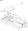
FIG. 1 is an exploded perspective view of a light emitter including an optical waveguide package according to an embodiment of the present disclosure. -
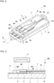
FIG. 2 is a perspective view of the light emitter inFIG. 1 without illustrating a sealing lid. -
FIG. 3 is a cross-sectional view of the light emitter taken along section line III-III inFIG. 2 . -
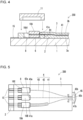
FIG. 4 is a cross-sectional view of the light-emitter taken along section line IV-IV inFIG. 2 . -
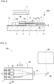
FIG. 5 is a plan view of the light emitter. -
FIG. 6 is an enlarged view of the light emitter illustrating a portion near emission ports. -
FIG. 7 is an exploded perspective view of a light emitter including an optical waveguide package according to another embodiment of the present disclosure. -
FIG. 8 is a cross-sectional view of the light emitter taken along section line VIII-VIII inFIG. 7 . -
FIG. 9 is a schematic diagram of a projection system according to an embodiment of the present disclosure. - Light-emitting elements that emit different colors (wavelengths) of light include light-emitting portions at different positions. Such light-emitting elements mounted on a substrate thus include the light-emitting portions at different distances from the surface of the substrate. Although the difference in distance may be as small as 1 µm or less, such a difference can greatly lower the efficiency of coupling with an optical waveguide. A known device described in
Patent Literature 1 allows a semiconductor laser, an optical component, and an optical waveguide to be aligned relative to one another. However, the technique described inPatent Literature 1 does not focus on any positional difference between light-emitting portions of light-emitting elements (semiconductor lasers) and thus may not avoid lowering the efficiency of coupling with the optical waveguide. A light emitter with highly efficient coupling with an optical waveguide is thus awaited. - A light emitter according to one or more embodiments of the present disclosure will now be described with reference to the accompanying drawings. In the present embodiment, an
optical waveguide package 100 includes asubstrate 1 including afirst surface 2, acladding 3 located on thefirst surface 2 and includingelement mount portions 8 each having an opening in athird surface 3b opposite to asecond surface 3a facing thefirst surface 2, and acore 4 located in thecladding 3. Theoptical waveguide package 100 further includes a sealinglid 11 and alens 45. - In the embodiment described in
FIGs. 1 to 5 , theoptical waveguide package 100 includeselement mount portions 8 on which afirst element 10A and asecond element 10B that are light-emitting elements are mountable. Alight emitter 200 includes theoptical waveguide package 100 and thefirst element 10A and thesecond element 10B. In the present embodiment, theoptical waveguide package 100 further includes anelement mount portion 8 on which athird element 10C that is a light-emitting element is mountable. Thelight emitter 200 includes thethird element 10C. In the embodiment of the present disclosure, thelight emitter 200 includes thethird element 10C, but is not limited to this structure and may include, for example, thefirst element 10A and thesecond element 10B alone. The light-emitting elements may be laser diodes. - The
substrate 1 includeselement mounts 6 in areas defined by theelement mount portions 8 on thefirst surface 2. Theelement mounts 6 join theelements first surface 2 of thesubstrate 1. Theelement mounts 6 may include, for example, metal members such as metalized layers on thefirst surface 2 of thesubstrate 1. The metal members in theelement mounts 6 may be joined to theelements element mounts 6 are connected toexternal wires 15. Theelements element mounts 6 to be electrically connected to, for example, an external power circuit through theexternal wires 15. Theexternal wires 15 may extend from inside theelement mount portions 8 to outside theelement mount portions 8. Theelements - In the present embodiment, light emitted from the
first element 10A (first light) and light emitted from thesecond element 10B (second light) have different colors. In the present embodiment, light emitted from thefirst element 10A, light emitted from thesecond element 10B, and light emitted from thethird element 10C (third light) have different colors. For example, light emitted from thefirst element 10A is red light, and light emitted from thesecond element 10B is green light. Light emitted from thethird element 10C is, for example, blue light. Thefirst element 10A is, for example, a laser diode including a gallium arsenide (GaAs) semiconductor. Thesecond element 10B and thethird element 10C are, for example, laser diodes each including a gallium nitride (GaN) semiconductor. Being made of different semiconductors, thefirst element 10A, thesecond element 10B, and thethird element 10C include light-emitting portions at different positions. - The
first surface 2 of thesubstrate 1 is flat at least in theelement mount portions 8. Thefirst element 10A, thesecond element 10B, and thethird element 10C mounted on the flat surface have different distances from thefirst surface 2 to their respective light-emitting portions. In the present embodiment, the distance from thefirst surface 2 to a light-emitting portion 10A1 of thefirst element 10A including a gallium arsenide semiconductor is greater than the distance from thefirst surface 2 to a light-emitting portion 10B1 of thesecond element 10B including a gallium nitride semiconductor. Thethird element 10C, including a gallium nitride semiconductor similarly to thesecond element 10B, has the same distance from thefirst surface 2 to its light-emitting portion as thesecond element 10B. - The
substrate 1 may be a ceramic wiring board containing a ceramic material. Examples of the ceramic material used for the ceramic wiring board include sintered aluminum oxide, sintered mullite, sintered silicon carbide, sintered aluminum nitride, and sintered glass ceramic. The ceramic wiring board may include conductors such as connection pads, internal wiring conductors, and external connection terminals for electrical connection between light-emitting and light-receiving elements and an external circuit. The ceramic wiring board may be a stack of layers. - The
substrate 1 may be an organic wiring board containing an organic material. The organic wiring board may be a printed wiring board, a build-up wiring board, or a flexible wiring board. Examples of the organic material used for the organic wiring board include an epoxy resin, a polyimide resin, a polyester resin, an acrylic resin, a phenolic resin, and a fluororesin. The organic wiring board may be a stack of layers. - The
substrate 1 may be made of a compound semiconductor such as GaN, GaAs, or indium phosphide (InP), or made of silicon (Si), germanium (Ge), or sapphire (Al2O3). - The
cladding 3 and thecore 4 may be made of, for example, glass such as quartz, or a resin. Both thecladding 3 and thecore 4 may be made of glass or a resin. In some embodiments, one of thecladding 3 or thecore 4 may be made of glass, and the other may be made of a resin. Thecore 4 and thecladding 3 have different refractive indexes, or more specifically, thecore 4 has a higher refractive index than thecladding 3. Light traveling through thecore 4 is fully reflected at the interfaces with thecladding 3 due to this difference in the refractive index. More specifically, a material with a higher refractive index is used to form a path, which is then surrounded by a material with a lower refractive index. This structure confines light in thecore 4 with the higher refractive index and allows the light to travel. - The
core 4 includes afirst core 41 corresponding to thefirst element 10A and asecond core 42 corresponding thesecond element 10B. Thecore 4 further includes athird core 43 corresponding to thethird element 10C. Thefirst core 41 includes afirst incident port 41a receiving the first light from thefirst element 10A mounted on the correspondingelement mount portion 8 and extends from thefirst incident port 41a in the direction away from theelement mount portion 8. Thesecond core 42 includes asecond incident port 42a receiving the second light from thesecond element 10B mounted on the correspondingelement mount portion 8 and extends from thesecond incident port 42a in the direction away from theelement mount portion 8. Thethird core 43 includes athird incident port 43a receiving the third light from thethird element 10C mounted on the correspondingelement mount portion 8 and extends from thethird incident port 43a in the direction away from theelement mount portion 8. - In the present embodiment, the
first core 41, thesecond core 42, and thethird core 43 are separate from one another in thecladding 3. Thefirst core 41 includes afirst emission port 41b at an end opposite to thefirst incident port 41a. Thesecond core 42 includes asecond emission port 42b at an end opposite to thesecond incident port 42a. Thethird core 43 includes athird emission port 43b at an end opposite to thethird incident port 43a. - Red light emitted from the
first element 10A enters thefirst core 41 through thefirst incident port 41a, travels through thefirst core 41, and is emitted through thefirst emission port 41b. Green light emitted from thesecond element 10B enters thesecond core 42 through thesecond incident port 42a, travels through thesecond core 42, and is emitted through thesecond emission port 42b. Blue light emitted from thethird element 10C enters thethird core 43 through thethird incident port 43a, travels through thethird core 43, and is emitted through thethird emission port 43b. In the present embodiment, both thefirst emission port 41b of thefirst core 41 and thesecond emission port 42b of thesecond core 42 are exposed at the end face of thecladding 3. Thethird emission port 43b of thethird core 43 is also exposed at the end face of thecladding 3. - In the
optical waveguide package 100 according to the present embodiment, a distance D1 from thefirst surface 2 of thesubstrate 1 to thefirst incident port 41a of thefirst core 41 differs from a distance D2 from thefirst surface 2 to thesecond incident port 42a of thesecond core 42. The distance D1 is from thefirst surface 2 to the middle of thefirst incident port 41a. The distance D2 is from thefirst surface 2 to the middle of thesecond incident port 42a. As described above, thefirst element 10A includes its light-emitting portion at a position different from the positions of the light-emitting portions of thesecond element 10B and thethird element 10C. Thefirst element 10A mounted on thefirst surface 2 of thesubstrate 1 thus has a distance from thefirst surface 2 to the light-emitting portion different from the distances from thesecond surface 2 to the light-emitting portions of thesecond element 10B and thethird element 10C. These distances correspond to the distance D1 and the distance D2. In the present embodiment, for example, the distance from thefirst surface 2 to the light-emitting portion 10A1 of thefirst element 10A is greater than the distance from thefirst surface 2 to the light-emitting portion 10B1 of thesecond element 10B. In this case, the distance D1 is set greater than the distance D2. Theoptical waveguide package 100 with this structure has less height position differences between the light-emitting elements and the emission ports of the cores, thus achieving highly efficient coupling with the core. Such highly accurate positioning is more likely to be achieved by adjusting the height position of thecore 4 by, for example, adjusting the thickness of the deposition film of thecladding 3 in manufacturing thecladding 3 and thecore 4 than by adjusting the height positions of the light-emitting elements in manufacturing thesubstrate 1 or postprocessing thefirst surface 2 as with known techniques. Thethird element 10C, which is the same or similar to thesecond element 10B, may have the distance from thefirst surface 2 to thethird incident port 43a of thethird core 43 that is the same as the distance D2 from thefirst surface 2 to thesecond incident port 42a of thesecond core 42. - The
lens 45 is located on the optical path of light emitted through each of thefirst emission port 41b and thesecond emission port 42b, and on the optical path of light emitted through thethird emission port 43b. Thelens 45 may be, for example, a condenser lens with a flat incident surface and a convex emission surface. - For example, the
light emitter 200 can be used as a light source for a projection system, as described later. Light emitted from the light emitter 200 (light passing through the lens 45) is reflected from a scanning mirror and reaches a screen. For example, the reflection angle of the scanning mirror is changed to cause light emitted from thelight emitter 200 to be projected at a different position on the screen. A color image can be displayed on the screen by continuously changing the position at which light is projected on the screen. -
FIG. 6 is an enlarged view of thelight emitter 200 illustrating a portion near the emission ports. In the present embodiment, a thickness T1 of thefirst core 41 is the same as a thickness T2 of thesecond core 42, and the difference between a distance D3 from thefirst surface 2 of thesubstrate 1 to thefirst emission port 41b of thefirst core 41 and a distance D4 from thefirst surface 2 of thesubstrate 1 to thesecond emission port 42b is less than or equal to half the thickness T1 of thefirst core 41. The thickness T1 of thefirst core 41 and the thickness T2 of thesecond core 42 being the same herein refers to the thickness T1 and the thickness T2 being set the same but their actual thicknesses being within ±20% of the set thicknesses to accommodate manufacturing variations in thecore 4 formed by film deposition. The distance D3 is from thefirst surface 2 to the middle of thefirst emission port 41b. The distance D4 is from thefirst surface 2 to the middle of thesecond emission port 42b. The thickness of thethird core 43 is also the same as the thickness of thefirst core 41, and the difference between the distance D3 from thefirst surface 2 of thesubstrate 1 to thefirst emission port 41b of thefirst core 41 and the distance from thefirst surface 2 of thesubstrate 1 to thethird emission port 43b may be less than or equal to half the thickness T1 of thefirst core 41. Red light from thefirst core 41 and green light from thesecond core 42 are emitted from the same position, and blue light from thethird core 43 is also emitted from the same position as the red light and the green light. In a projection system including thelight emitter 200 described above, the three colors of light beams emitted from the same position facilitate control of the timing to emit light from each light-emitting element and the timing to change the reflection angle of the scanning mirror. - The sealing
lid 11 covering theelement mount portions 8 is on thethird surface 3b of thecladding 3. The sealinglid 11 airtightly seals the space accommodating theelements first surface 2 of thesubstrate 1, theelement mount portions 8, and the sealing lid 11). The sealinglid 11 may be made of a glass material such as quartz, borosilicate, or sapphire. The sealinglid 11 may be made of a metal such as Fe, Ni, or Co, an alloy containing one or more of these metals, or silicon. -
FIG. 7 is an exploded perspective view of alight emitter 200A including anoptical waveguide package 100 A according to another embodiment of the present disclosure.FIG. 8 is a cross-sectional view of thelight emitter 200A taken along section line VIII-VIII inFIG. 7 . The same reference numerals denote the components corresponding to those in the above embodiment, and such components will not be described repeatedly. The present embodiment differs from the above embodiment in that thefirst core 41 and thesecond core 42 merge at amerging point 50 in thecladding 3. In the present embodiment, thethird core 43 also merges at themerging point 50. The cores merge together into a single joiningpath 51 at themerging point 50 to emit light through anemission port 52. More specifically, red light traveling through thefirst core 41, green light traveling through thesecond core 42, and blue light traveling through thethird core 43 merge at themerging point 50 to travel through the joiningpath 51 before being emitted through theemission port 52 as a single beam of merged light. A projection system including thelight emitter 200 described above can use the merged light as a single beam of light that is easily controllable. - In the structure including the
merging point 50 as in the present embodiment, merging of thefirst core 41 and thesecond core 42 refers to merging of thefirst core 41 with thesecond core 42. As described above, thefirst incident port 41a of thefirst core 41 is located more distant from thefirst surface 2 than thesecond incident port 42a of thesecond core 42. In thesecond core 42, the distance from thefirst surface 2 is constant between thesecond incident port 42a and themerging point 50. In thefirst core 41, the distance D1 from thefirst surface 2 decreases to the distance D2 between thefirst incident port 41a and themerging point 50. In thefirst core 41, the distance D1 from thefirst surface 2 may change to the distance D2 continuously or intermittently between thefirst incident port 41a and themerging point 50. In the present embodiment, thefirst core 41 includes afirst bend 61 and asecond bend 62 between thefirst incident port 41a and themerging point 50. Thefirst bend 61 is located closer to thefirst incident port 41a than thesecond bend 62. The distance from thefirst surface 2 of thesubstrate 1 starts changing at thefirst bend 61. The distance from thefirst surface 2 of thesubstrate 1 stops changing at thesecond bend 62. Thefirst core 41 has a constant distance from thefirst surface 2 and extends parallel to thefirst surface 2 between thefirst incident port 41a and thefirst bend 61. The distance from thefirst surface 2 continuously decreases between thefirst bend 61 and thesecond bend 62. Thefirst core 41 has a distance D5 from thefirst surface 2 between thesecond bend 62 and themerging point 50. The distance D5 is equal to the distance D2 ± half the thickness T1 of thefirst core 41. Thefirst core 41 has the constant distance D5 from thefirst surface 2 and extends parallel to thefirst surface 2 between thesecond bend 62 and themerging point 50, and merges with thesecond core 42 at themerging point 50. Theoptical waveguide package 100A with this structure has less scattering of light resulting from red light traveling through thefirst core 41 merging with green light traveling through thesecond core 42 at themerging point 50, thus causing less loss of emitted light. - In the
optical waveguide packages light emitters FIGs. 1 to 8 , thecladding 3 includes theelement mount portions 8 as through-holes, but is not limited to this structure. Theelement mount portions 8 may be recesses being open on thethird surface 3b, rather than the through-holes. Thecladding 3 may be a plate including the incident port and the emission port of thecore 4. -
FIG. 9 is a schematic diagram of aprojection system 500 according to an embodiment of the present disclosure. Theprojection system 500 includes thelight emitter 200 and ascreen 400. Thescreen 400 is located on the optical path of light emitted from thelight emitter 200. Theprojection system 500 may include thelight emitter 200A instead of thelight emitter 200. In the present embodiment, theprojection system 500 further includes ascanning mirror 300. Light emitted from thelight emitter 200 is reflected from thescanning mirror 300 and has its optical path redirected to be projected on thescreen 400. For example, the reflection angle of thescanning mirror 300 is changed to cause light emitted from thelight emitter 200 to be projected at a different position on thescreen 400. A color image can be displayed on thescreen 400 by continuously changing the position at which light is projected on thescreen 400. - The
scanning mirror 300 may be any device that can change the reflection angle precisely and continuously in a short time. For example, a micromirror using micro electromechanical systems (MEMS) may be used. Thescanning mirror 300 may be, for example, a polygon scanner, a galvanometer scanner, or a resonant scanner, other than a micromirror. Thescreen 400 may be a diffuse screen, a retrograde screen, a reflective screen, or a rear screen. Thescreen 400 may also be the retina of an observer. - In still another embodiment of the present disclosure, the
elements - The present disclosure may be implemented in the following forms.
- In an embodiment of the present disclosure, an optical waveguide package includes a substrate including a first surface, a cladding located on the first surface, including a second surface facing the first surface and a third surface opposite to the second surface, and including an element mount portion with an opening in the third surface, a first core including a first incident port to receive first light from a first element mounted on the element mount portion and extending from the first incidence port in a direction away from the element mount portion, and a second core including a second incident port to receive second light from a second element mounted on the element mount portion and extending from the second incidence port in a direction away from the element mount portion. A distance D1 from the first surface to the first incident port differs from a distance D2 from the first surface to the second incident port.
- In another embodiment of the present disclosure, a light emitter includes the optical waveguide package described above, and a first element and a second element connected to the element mount portion. The distance D1 corresponds to a distance from the first surface to a light-emitting portion of the first element. The distance D2 corresponds to a distance from the first surface to a light-emitting portion of the second element.
- In another embodiment of the present disclosure, a projection system includes the light emitter described above, and a screen located on an optical path of light emitted from the light emitter.
- In one or more embodiments of the present disclosure, the optical waveguide package and the light emitter can have highly efficient coupling with an optical waveguide.
- Although embodiments of the present disclosure have been described in detail, the present disclosure is not limited to the embodiments described above, and may be changed or varied in various manners without departing from the spirit and scope of the present disclosure. The components described in the above embodiments may be entirely or partially combined as appropriate unless any contradiction arises.
-
- 1
- substrate
- 2
- first surface
- 3
- cladding
- 3a
- second surface
- 3b
- third surface
- 4
- core
- 6
- element mount
- 8
- element mount portion
- 10A
- first element
- 10A1
- light-emitting portion
- 10B
- second element
- 10B1
- light-emitting portion
- 10C
- third element
- 11
- sealing lid
- 15
- external wire
- 41
- first core
- 41a
- first incident port
- 41b
- first emission port
- 42
- second core
- 42a
- second incident port
- 42b
- second emission port
- 43
- third core
- 43a
- third incident port
- 43b
- third emission port
- 45
- lens
- 50
- merging point
- 51
- joining path
- 52
- emission end face
- 100, 100A
- optical waveguide package
- 200, 200A
- light emitter
- 300
- scanning mirror
- 400
- screen
- 500
- projection system
Claims (6)
- An optical waveguide package, comprising:a substrate including a first surface;a cladding on the first surface, the cladding including a second surface facing the first surface and a third surface opposite to the second surface, the cladding including an element mount portion with an opening in the third surface;a first core including a first incident port to receive first light from a first element mounted on the element mount portion, the first core extending from the first incidence port in a direction away from the element mount portion; anda second core including a second incident port to receive second light from a second element mounted on the element mount portion, the second core extending from the second incidence port in a direction away from the element mount portion,wherein a distance (D1) from the first surface to the first incident port differs from a distance (D2) from the first surface to the second incident port.
- The optical waveguide package according to claim 1, whereinthe first core includes a first emission port for the first light,the second core includes a second emission port for the second light,the first core has a same thickness as the second core, anda difference between a distance (D3) from the first surface to the first emission port and a distance (D4) from the first surface to the second emission port is less than or equal to half the thickness of the first core.
- The optical waveguide package according to claim 1, wherein
the first core and the second core merge with each other at a merging point in the cladding. - The optical waveguide package according to claim 3, whereinthe first core includes a first bend and a second bend between the first incident port and the merging point,the first bend is closer to the first incident port than the second bend and is a point at which the distance from the first surface starts changing, andthe second bend is a point at which the distance from the first surface stops changing, and a distance (D5) from the first surface between the second bend and the merging point is equal to the distance (D2) ± half the thickness of the first core.
- A light emitter, comprising:the optical waveguide package according to any one of claims 1 to 4; anda first element and a second element connected to the element mount portion,wherein the distance (D1) corresponds to a distance from the first surface to a light-emitting portion of the first element, andthe distance (D2) corresponds to a distance from the first surface to a light-emitting portion of the second element.
- A projection system, comprising:the light emitter according to claim 5; anda screen located on an optical path of light emitted from the light emitter.
Applications Claiming Priority (2)
| Application Number | Priority Date | Filing Date | Title |
|---|---|---|---|
| JP2020142961 | 2020-08-26 | ||
| PCT/JP2021/028639 WO2022044714A1 (en) | 2020-08-26 | 2021-08-02 | Optical waveguide package, light-emitting device, and projection system |
Publications (1)
| Publication Number | Publication Date |
|---|---|
| EP4206766A1 true EP4206766A1 (en) | 2023-07-05 |
Family
ID=80352238
Family Applications (1)
| Application Number | Title | Priority Date | Filing Date |
|---|---|---|---|
| EP21861142.4A Withdrawn EP4206766A1 (en) | 2020-08-26 | 2021-08-02 | Optical waveguide package, light-emitting device, and projection system |
Country Status (5)
| Country | Link |
|---|---|
| US (1) | US20230324780A1 (en) |
| EP (1) | EP4206766A1 (en) |
| JP (1) | JPWO2022044714A1 (en) |
| CN (1) | CN115943334A (en) |
| WO (1) | WO2022044714A1 (en) |
Families Citing this family (3)
| Publication number | Priority date | Publication date | Assignee | Title |
|---|---|---|---|---|
| WO2025070157A1 (en) * | 2023-09-28 | 2025-04-03 | 京セラ株式会社 | Optical waveguide, package for housing electronic element, electronic module, and electronic device |
| WO2025070158A1 (en) * | 2023-09-28 | 2025-04-03 | 京セラ株式会社 | Optical waveguide substrate, package for housing electronic element, electronic module, and electronic device |
| WO2026070515A1 (en) * | 2024-09-27 | 2026-04-02 | 京セラ株式会社 | Optical waveguide substrate, light-emitting device, and electronic device |
Family Cites Families (17)
| Publication number | Priority date | Publication date | Assignee | Title |
|---|---|---|---|---|
| DE19549395A1 (en) * | 1995-02-07 | 1996-10-31 | Ldt Gmbh & Co | Image generation system for detecting and treating sight defects |
| JP2002014246A (en) * | 2000-06-27 | 2002-01-18 | Matsushita Electric Works Ltd | Optical waveguide and method for manufacturing the same |
| JP4333030B2 (en) * | 2000-12-26 | 2009-09-16 | 株式会社村田製作所 | Optical waveguide and method for manufacturing the same |
| JP4200436B2 (en) * | 2002-12-05 | 2008-12-24 | ソニー株式会社 | Polymer optical waveguide |
| KR100637929B1 (en) * | 2004-11-03 | 2006-10-24 | 한국전자통신연구원 | Hybrid optical element |
| US9927611B2 (en) * | 2010-03-29 | 2018-03-27 | Soraa Laser Diode, Inc. | Wearable laser based display method and system |
| JP2012114145A (en) | 2010-11-22 | 2012-06-14 | Shinko Electric Ind Co Ltd | Light generation device |
| US9052481B2 (en) * | 2013-09-17 | 2015-06-09 | Telefonaktiebolaget L M Ericsson (Publ) | Method, apparatus and optical interconnect manufactured by 3D printing |
| US9323012B1 (en) * | 2014-10-27 | 2016-04-26 | Laxense Inc. | Hybrid integrated optical device with high alignment tolerance |
| CN106062600B (en) * | 2014-11-11 | 2020-07-07 | 光研公司 | Light beam combiner and chip type multi-wavelength laser light source |
| WO2017090333A1 (en) * | 2015-11-27 | 2017-06-01 | シャープ株式会社 | Optical waveguide element and light source module |
| WO2017123309A2 (en) * | 2016-01-06 | 2017-07-20 | Northwestern University | Monolithical widely tunable quantum cascade laser devices |
| US20200185877A1 (en) * | 2016-06-29 | 2020-06-11 | Sharp Kabushiki Kaisha | Optical module |
| WO2019083773A1 (en) * | 2017-10-26 | 2019-05-02 | Corning Optical Communications LLC | Optical assemblies, interconnection substrates and methods for forming optical links in interconnection substrates |
| JP7060798B2 (en) * | 2018-05-30 | 2022-04-27 | 日亜化学工業株式会社 | Light source device |
| WO2020026730A1 (en) * | 2018-07-30 | 2020-02-06 | パナソニック株式会社 | Semiconductor light emitting device and external resonance type laser device |
| DE102018217745A1 (en) * | 2018-10-17 | 2020-04-23 | Robert Bosch Gmbh | Device and method for providing a multicolored light beam for a projector, projector and manufacturing method for producing a device for providing a multicolored light beam for a projector |
-
2021
- 2021-08-02 US US18/021,867 patent/US20230324780A1/en not_active Abandoned
- 2021-08-02 WO PCT/JP2021/028639 patent/WO2022044714A1/en not_active Ceased
- 2021-08-02 JP JP2022545588A patent/JPWO2022044714A1/ja active Pending
- 2021-08-02 CN CN202180050898.1A patent/CN115943334A/en active Pending
- 2021-08-02 EP EP21861142.4A patent/EP4206766A1/en not_active Withdrawn
Also Published As
| Publication number | Publication date |
|---|---|
| WO2022044714A1 (en) | 2022-03-03 |
| CN115943334A (en) | 2023-04-07 |
| US20230324780A1 (en) | 2023-10-12 |
| JPWO2022044714A1 (en) | 2022-03-03 |
Similar Documents
| Publication | Publication Date | Title |
|---|---|---|
| EP4174538A1 (en) | Optical waveguide package, light-emitting device, and projection system | |
| EP4206766A1 (en) | Optical waveguide package, light-emitting device, and projection system | |
| JP7824543B2 (en) | Light-emitting module manufacturing method, light-emitting module, and projector | |
| US11967803B2 (en) | Method of manufacturing light emitting module, light emitting module, and projector | |
| EP4040516A1 (en) | Optical waveguide package and light emitting device | |
| JP2019207976A (en) | Light source device | |
| JP2013143480A (en) | Light-emitting device, manufacturing method of the same and projector | |
| JP2026015607A (en) | Light-emitting device and backlight | |
| US20240079848A1 (en) | Optical module | |
| CN102096291B (en) | Light emitting device and projector | |
| JP5429479B2 (en) | Light emitting device and projector | |
| EP4400879A1 (en) | Light-emitting device | |
| EP4297206A1 (en) | Light emitting device | |
| US12276823B2 (en) | Light source module | |
| CN116316044A (en) | Manufacturing method of light-emitting device, light-emitting device | |
| US12055752B2 (en) | Light-emitting device and light-emitting module | |
| US12292590B2 (en) | Light source module | |
| US20250306319A1 (en) | Optical waveguide package and light-emitting device | |
| EP4297205A1 (en) | Light emitting device | |
| US20260039084A1 (en) | Light-emitting device | |
| JP2017219625A (en) | Light source device and projector | |
| US20240069293A1 (en) | Optical module | |
| JP2017220529A (en) | Light source device manufacturing method, light source device, and projector | |
| JP2024104946A (en) | Light-emitting device |
Legal Events
| Date | Code | Title | Description |
|---|---|---|---|
| STAA | Information on the status of an ep patent application or granted ep patent |
Free format text: STATUS: THE INTERNATIONAL PUBLICATION HAS BEEN MADE |
|
| PUAI | Public reference made under article 153(3) epc to a published international application that has entered the european phase |
Free format text: ORIGINAL CODE: 0009012 |
|
| STAA | Information on the status of an ep patent application or granted ep patent |
Free format text: STATUS: REQUEST FOR EXAMINATION WAS MADE |
|
| 17P | Request for examination filed |
Effective date: 20230213 |
|
| AK | Designated contracting states |
Kind code of ref document: A1 Designated state(s): AL AT BE BG CH CY CZ DE DK EE ES FI FR GB GR HR HU IE IS IT LI LT LU LV MC MK MT NL NO PL PT RO RS SE SI SK SM TR |
|
| DAV | Request for validation of the european patent (deleted) | ||
| DAX | Request for extension of the european patent (deleted) | ||
| STAA | Information on the status of an ep patent application or granted ep patent |
Free format text: STATUS: THE APPLICATION HAS BEEN WITHDRAWN |
|
| 18W | Application withdrawn |
Effective date: 20240527 |