EP4206635A1 - Piezoelectric sensor, fabrication method therefor, and haptic feedback device - Google Patents
Piezoelectric sensor, fabrication method therefor, and haptic feedback device Download PDFInfo
- Publication number
- EP4206635A1 EP4206635A1 EP21942395.1A EP21942395A EP4206635A1 EP 4206635 A1 EP4206635 A1 EP 4206635A1 EP 21942395 A EP21942395 A EP 21942395A EP 4206635 A1 EP4206635 A1 EP 4206635A1
- Authority
- EP
- European Patent Office
- Prior art keywords
- thin film
- film layer
- piezoelectric thin
- layer
- piezoelectric
- Prior art date
- Legal status (The legal status is an assumption and is not a legal conclusion. Google has not performed a legal analysis and makes no representation as to the accuracy of the status listed.)
- Granted
Links
Images


Classifications
-
- H—ELECTRICITY
- H10—SEMICONDUCTOR DEVICES; ELECTRIC SOLID-STATE DEVICES NOT OTHERWISE PROVIDED FOR
- H10N—ELECTRIC SOLID-STATE DEVICES NOT OTHERWISE PROVIDED FOR
- H10N30/00—Piezoelectric or electrostrictive devices
- H10N30/30—Piezoelectric or electrostrictive devices with mechanical input and electrical output, e.g. functioning as generators or sensors
- H10N30/302—Sensors
-
- G—PHYSICS
- G01—MEASURING; TESTING
- G01L—MEASURING FORCE, STRESS, TORQUE, WORK, MECHANICAL POWER, MECHANICAL EFFICIENCY, OR FLUID PRESSURE
- G01L1/00—Measuring force or stress, in general
- G01L1/16—Measuring force or stress, in general using properties of piezoelectric devices
-
- G—PHYSICS
- G06—COMPUTING OR CALCULATING; COUNTING
- G06F—ELECTRIC DIGITAL DATA PROCESSING
- G06F3/00—Input arrangements for transferring data to be processed into a form capable of being handled by the computer; Output arrangements for transferring data from processing unit to output unit, e.g. interface arrangements
- G06F3/01—Input arrangements or combined input and output arrangements for interaction between user and computer
- G06F3/016—Input arrangements with force or tactile feedback as computer generated output to the user
-
- H—ELECTRICITY
- H10—SEMICONDUCTOR DEVICES; ELECTRIC SOLID-STATE DEVICES NOT OTHERWISE PROVIDED FOR
- H10N—ELECTRIC SOLID-STATE DEVICES NOT OTHERWISE PROVIDED FOR
- H10N30/00—Piezoelectric or electrostrictive devices
- H10N30/01—Manufacture or treatment
-
- G—PHYSICS
- G06—COMPUTING OR CALCULATING; COUNTING
- G06F—ELECTRIC DIGITAL DATA PROCESSING
- G06F3/00—Input arrangements for transferring data to be processed into a form capable of being handled by the computer; Output arrangements for transferring data from processing unit to output unit, e.g. interface arrangements
- G06F3/01—Input arrangements or combined input and output arrangements for interaction between user and computer
- G06F3/03—Arrangements for converting the position or the displacement of a member into a coded form
- G06F3/041—Digitisers, e.g. for touch screens or touch pads, characterised by the transducing means
- G06F3/044—Digitisers, e.g. for touch screens or touch pads, characterised by the transducing means by capacitive means
- G06F3/0443—Digitisers, e.g. for touch screens or touch pads, characterised by the transducing means by capacitive means using a single layer of sensing electrodes
Definitions
- the present disclosure relates to the field of sensor technology, in particular to a piezoelectric sensor, a fabrication method therefor, and a haptic feedback device.
- Haptic feedback (known as Haptics) is the focus of today's technology development, and in particular, haptic feedback enables the terminal to interact with the human body through touch. Haptic feedback, in turn, can be divided into two categories, one is vibration feedback and the other is tactile reproduction technology.
- the present disclosure provides a piezoelectric sensor, a fabrication method therefor, and a haptic feedback device. And, the solution is as follows.
- An embodiment of the present disclosure provides a piezoelectric sensor, including: a base substrate, and a first electrode layer, a piezoelectric thin film layer, an insulating layer, and a second electrode layer which are arranged in sequence away from the base substrate, where the insulating layer is in contact with at least part of the piezoelectric thin film layer.
- a side of the piezoelectric thin film layer facing away from the base substrate includes at least one hollow structure, and each of the at least one hollow structures is filled with the insulating layer.
- an orthographic projection of the piezoelectric thin film layer on the base substrate covers an orthographic projection of the insulating layer on the base substrate.
- an orthographic projection of the insulating layer on the base substrate and an orthographic projection of the piezoelectric thin film layer on the base substrate overlap each other.
- a material of the insulating layer includes at least one of polyimide, silica, or alumina.
- a thickness of the insulating layer and a thickness of the piezoelectric thin film layer satisfy a following relationship: d PI ⁇ 0.1 * d PZT ; where d PI represents the thickness of the insulating layer and d PZT represents the thickness of the piezoelectric thin film layer.
- a thickness of the insulating layer is greater than or equal to 50 nm; and the thickness of the insulating layer is less than or equal to 200 nm.
- a thickness of the piezoelectric thin film layer is greater than 0; and the thickness of the piezoelectric thin film layer is less than or equal to 2 ⁇ m.
- a capacitance of the piezoelectric thin film layer and a capacitance of the insulating layer satisfy a following relationship: C PI ⁇ 100 C PZT ; where C PI represents the capacitance of the piezoelectric thin film layer and C PZT represents the capacitance of the insulating layer.
- a resistance of the piezoelectric thin film layer and a resistance of the insulating layer satisfy a following relationship: R PI ⁇ 1000 R PZT ; where R PI represents the resistance of the piezoelectric thin film layer and R PZT represents the resistance of the insulating layer.
- a side of the piezoelectric thin film layer facing away from the base substrate is provided with a lyophilic material layer.
- a material of the piezoelectric thin film layer includes at least one of aluminum nitride, zinc oxide, lead zirconate titanate, barium titanate, lead titanate, potassium niobate, lithium niobate, lithium tantalate, or lanthanum gallium silicate.
- a side of the first electrode layer close to the piezoelectric thin film layer is provided with a plurality of first columnar structures.
- a side of the second electrode layer facing the piezoelectric thin film layer is provided with a plurality of second columnar structures.
- a side of the first electrode layer facing the piezoelectric thin film layer is provided with a plurality of third columnar structures
- the side of the second electrode layer facing the piezoelectric thin film layer is provided with a plurality of fourth columnar structures
- an orthographic projection of each of the third columnar structures on the base substrate does not overlap with an orthographic projection of each of the fourth columnar structures on the base substrate.
- an embodiment of the present disclosure provides a haptic feedback device, including a haptic feedback circuit and a piezoelectric sensor as described in any one of the above; where:
- an embodiment of the present disclosure provides a fabrication method for a piezoelectric sensor, including:
- the forming the insulating layer being in contact with at least part of the piezoelectric thin film layer on the side of the piezoelectric thin film layer facing away from the first electrode layer includes:
- the thin film piezoelectric material has the characteristics of high dielectric constant and transparency, and is well-suited for screen-integrated vibrator structures, when the surface charge distribution is uneven to lead accumulation or the voltage is too high, the vibrator undergoes breakdown phenomena, for example, the upper and lower electrodes remain open, but the piezoelectric thin film layer structure is damaged, and for another example, the upper and lower electrodes are short-circuited due to breakdown, resulting in failure of the entire vibrator.
- the main cause of short circuit is the stress of particles, granules or films in the process, which leads to cracks in the piezoelectric film layer. In this crack state, if the electrode is directly deposited on the piezoelectric film layer, it will lead to high short circuit risk. Therefore, how to avoid short circuit of the piezoelectric sensor has become an urgent technical problem to be solved.
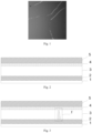
- Fig. 1 is a schematic top view of a piezoelectric layer with cracks in a thin film vibration chip in the related art, during the process, the stress of particles, granules or films leads to cracks in the piezoelectric layer, and if the electrode is deposited directly on the piezoelectric layer, the cracks will lead to short circuit of the thin film vibration chip, thus reducing product yield.
- embodiments of the present disclosure provide a piezoelectric sensor, a fabrication method therefor, and a haptic feedback device for avoiding short circuits in the piezoelectric sensor and improving product yield.
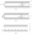
- Fig. 2 is a schematic structural diagram of a piezoelectric sensor according to an embodiment of the present disclosure, and the piezoelectric sensor, including: a base substrate 1, and a first electrode layer 2, a piezoelectric thin film layer 3, an insulating layer 4 and a second electrode layer 5 which are arranged in sequence away from the base substrate 1, where the insulating layer 4 is in contact with at least part of the piezoelectric thin film layer 3.
- the base substrate 1 can be a substrate made of glass, or silicon or silicon dioxide (SiO 2 ), or sapphire, or metal wafer, which is not limited here, and the skilled person can set up the base substrate 1 according to the needs of the actual application.
- the first electrode layer 2 may be made of indium tin oxide (ITO), the first electrode layer 2 can also be made of indium zinc oxide (IZO), or one of titanium gold (Ti-Au) alloy, titanium aluminum titanium (Ti-Al-Ti) alloy, titanium molybdenum (TiMo) alloy, and in addition, the first electrode layer 2 may be made of one of titanium (Ti), gold (Au), silver (Ag), molybdenum (Mo), copper (Cu), tungsten (W), and chromium (Cr), and the skilled person can arrange the first electrode layer 2 according to the needs of the actual application, which is not limited here. Accordingly, the second electrode layer 5 may also be made of the same material as the first electrode layer 2, which is not described in detail here.
- a material of the piezoelectric thin film layer 3 may include at least one of aluminum nitride (AIN), ZnO (zinc oxide), lead zirconate titanate (Pb (Zr, Ti)O 3 , PZT), barium titanate (BaTiO 3 ), lead titanate (PbTiO 3 ), potassium niobate (KNbO 3 ), lithium niobate (LiNbO 3 ), lithium tantalate (LiTaO 3 ), or gallium lanthanum silicate (La 3 Ga 5 SiO 14 ), in this way, the vibration characteristics of the piezoelectric sensor are guaranteed while at the same time the piezoelectric sensor is transparent, in particular the material from which the piezoelectric thin film layer 3 is made can be selected according to the actual usage needs of the person skilled in the art, which is not limited here.
- the piezoelectric thin film layer 3 is made using PZT, the piezoelectric properties of the respective piezoelectric sensor are guaranteed since the PZT has a high electric coefficient, the respective piezoelectric sensor can be applied in a haptic feedback device, and the PZT has high light transmittance that does not affect the display quality of the display device when it is integrated into the display device.
- the insulating layer 4 between the piezoelectric thin film layer 3 and the second electrode layer 5 is in contact with at least part of the piezoelectric thin film layer 3, the insulating layer 4 may be in contact with all of the piezoelectric thin film layer 3, for example, the insulating layer 4 completely covers the side of the piezoelectric thin film layer 3 facing away from the base substrate 1, Fig.
- the insulating layer 4 completely covers the side of the piezoelectric thin film layer 3 facing away from the base substrate 1, and may also be in contact with a part of the piezoelectric thin film layer 3, for example, the insulating layer 4 fills only cracks in the piezoelectric thin film layer 3, for another example, the insulating layer 4 is disposed only within a portion of the area of the piezoelectric thin film layer 3 facing away from the base substrate 1.
- the piezoelectric thin film layer 3 may be arranged entirely on a side of the first electrode layer 2 facing away from the base substrate 1, the efficiency of fabrication of the piezoelectric sensor is improved, and in addition, the piezoelectric thin film layer 3 can be patterned as needed, for example, the piezoelectric thin film layer 3 is arranged in areas on the side of the first electrode layer 2 facing away from the base substrate 1, thereby enabling flexible design of the piezoelectric sensor.
- the insulating layer 4 since the insulating layer 4 is in contact with at least part of the piezoelectric thin film layer 3, even in the presence of cracks in the piezoelectric thin film layer 3, by means of the insulating layer 4 it is possible to effectively fill the cracks.
- the existence of the insulating layer 4 prevents the short circuit between the second electrode layer 5 and the first electrode layer 2 due to contact, thereby avoiding the short circuit risk of the piezoelectric sensor and improving the product yield.
- Fig. 3 is a schematic structural diagram of the piezoelectric sensor, the piezoelectric thin film layer 3 includes at least one hollow structure f on the side facing away from the base substrate 1, each of the hollow structures f being filled with the insulating layer 4.
- There may be one or a plurality of hollow structures f and the case of one hollow structure f is illustrated in Fig. 3 , and of course there may be a plurality of hollow structures f, which is not limited herein.
- the hollow structure f may be a crack present in the piezoelectric thin film layer 3.
- the sizes of the hollow structures f may be unequal, the distribution of which may be randomly distributed according to actual process conditions.
- the insulating layer 4 completely fills each of the hollow structures f, and the thickness of the insulating layer 4 filled in each of the hollow structures f is equal to the depth of the respective hollow structure f, both the thickness direction of the insulating layer 4 and the depth direction of the hollow structure f are in a direction perpendicular to the plane of the base substrate 1, the term "equal" is not exactly equal, may be approximately equal, or roughly equal.
- each of the hollow structures f in the piezoelectric thin film layer 3 is effectively filled by the insulating layer 4, thus avoiding the risk of short circuits of the piezoelectric sensor, moreover, since the insulating layer 4 completely fills each of the hollow structures f, when other parts of the insulating layer 4 completely cover the side of the piezoelectric thin film layer 3 facing away from the base substrate 1 except for the part filled to each of the hollow structures f, the flush arrangement of the side of the piezoelectric thin film layer 3 away from the base substrate 1 is realized, thus ensuring the structural stability of the piezoelectric sensor made later and improving the service performance of the piezoelectric sensor.
- the orthographic projection of the insulating layer 4 on the base substrate 1 falls entirely within the area of the orthographic projection of the piezoelectric thin film layer 3 on the base substrate 1.
- the orthographic projection of the insulating layer 4 on the base substrate 1 and the orthographic projection of the piezoelectric thin film layer 3 on the base substrate 1 overlap with each other.
- the insulating layer 4 may completely cover the side of the piezoelectric thin film layer 3 facing away from the base substrate 1, and even when the piezoelectric thin film layer 3 originally has cracks, the hollow structure f is effectively filled through the insulating layer 4, thus avoiding the short circuit risk of the piezoelectric sensor and improving the product yield.
- the insulating layer 4 includes at least one of polyimide (PI), silica (SiO 2 ), alumina (Al 2 O 3 ).
- PI polyimide
- SiO 2 silica
- Al 2 O 3 alumina
- the insulating layer 4 may flow through gravitational leveling into the hollow structure f, for example, when PI is coated on the side of the piezoelectric thin film layer 3 facing away from the base substrate 1 using a wet process, since PI has better leveling properties at the surface of the piezoelectric thin film layer 3, PI may quickly level the hollow structure f, while ensuring surface planarity on the side of the piezoelectric thin film layer 3 facing away from the base substrate 1 and avoiding the risk of short circuits of the piezoelectric sensor, since PI has the better high temperature curing (cyclization) property, after PI wet coating on the side
- SiO 2 may also be coated on the side of the piezoelectric thin film layer 3 facing away from the base substrate 1 using a wet process, thereby leveling the hollow structure f, ensuring surface planarity on the side of the piezoelectric thin film layer 3 facing away from the base substrate 1, and avoiding the risk of short circuits of the piezoelectric sensor, after SiO 2 wet coating on the side of the piezoelectric thin film layer 3 facing away from the base substrate 1, the insulating layer 4 is formed by high temperature curing of SiO 2 at not less than 300°C, thereby ensuring stable insulating properties of the insulating layer 4 and improving the performance of the piezoelectric sensor.
- a dry deposition process may also be used to coat Al 2 O 3 on the side of the piezoelectric thin film layer 3 facing away from the base substrate 1, avoiding the risk of short circuits of the piezoelectric sensor due to the insulation property of Al 2 O 3 and further improving the performance of the piezoelectric sensor.
- the piezoelectric thin film layer 3 may be arranged in other ways and will not be described in detail herein.
- the thickness of the insulating layer 4 and the thickness of the piezoelectric thin film layer 3 satisfy the following relationship: d PI ⁇ 0.1 * d PZT ; where d PI represents the thickness of the insulating layer 4 and d PZT represents the thickness of the piezoelectric thin film layer 3.
- the inventors found in practical studies that, at a certain thickness of the piezoelectric thin film layer 3, the thickness of the insulating layer 4 coated on a side of the piezoelectric thin film layer 3 facing away from the base substrate 1 is set to be less than 10% of the thickness of the piezoelectric thin film layer 3, for example, when the thickness of the piezoelectric thin film layer 3 is 2 ⁇ m, the insulating layer 4 may have a thickness of 200 nm, it can be 100 nm or 50 nm, and is not limited herein, the insulating properties of the insulating layer 4 can be guaranteed, so that the risk of short circuits of the piezoelectric sensor is avoided and the vibration properties of the piezoelectric sensor during high frequency AC driving are guaranteed, thus improving the performance of the piezoelectric sensor.
- a thickness of the insulating layer 4 is greater than or equal to 50 nm; and the thickness of the insulating layer 4 is less than or equal to 200 nm.
- the insulating layer 4 has a thickness between 50 nm and 200 nm, such as 100 nm, 60 nm, or 50 nm, the insulating layer 4 has better insulating properties when the thickness of the insulating layer 4 is in the above range, thus effectively avoiding the risk of short circuits of the piezoelectric sensor.
- a thickness of the piezoelectric thin film layer 3 is greater than 0; and the thickness of the piezoelectric thin film layer 3 is less than or equal to 2 ⁇ m.
- the thickness of the piezoelectric thin film layer 3 is between 0 ⁇ 2 ⁇ m, for example, the thickness of the piezoelectric thin film layer 3 is 0.5 ⁇ m, for another example, the thickness of the piezoelectric thin film layer 3 is 1 ⁇ m, and for another example, the thickness of the piezoelectric thin film layer 3 is 2 ⁇ m, and in practical applications, the thickness of the piezoelectric thin film layer 3 may be set as close to zero as possible, thus taking into account a lightly thinned design of the piezoelectric sensor while ensuring better vibration properties of the piezoelectric thin film layer 3.
- a capacitance of the piezoelectric thin film layer 3 and a capacitance of the insulating layer 4 satisfy the following relationship: C PI ⁇ 100 C PZT ; where C PI represents the capacitance of the piezoelectric thin film layer 3 and C PZT represents the capacitance of the insulating layer 4.
- the capacitance of the piezoelectric thin film layer 3 and the capacitance of the insulating layer 4 satisfies the relationship: C PI ⁇ 100C PZT
- the voltage loaded on the piezoelectric thin film layer 3 is: V PZT ⁇ 1 / j ⁇ C PZT 1 / j ⁇ C PI + 1 / j ⁇ C PZT V AC ⁇ V AC .
- the capacitance of the piezoelectric thin film layer 3 is certain, according to the capacitance relationship between the piezoelectric thin film layer 3 and the insulating layer 4 described above, the material as well as the thickness of the insulating layer 4 is selected, the dielectric constant of the insulating layer 4 ranges from 2.3 ⁇ 2.8 when the insulating layer 4 is made of PI material, the insulating layer 4 can be arranged according to the circumstances of the piezoelectric thin film layer 3 in practical applications, thereby enabling flexible preparation of the piezoelectric sensor.
- the resistance of the piezoelectric thin film layer 3 and the resistance of the insulating layer 4 satisfy the following relationship: R PI ⁇ 1000 R PZT ; where R PI represents the resistance of the piezoelectric thin film layer 3 and R PZT represents the resistance of the insulating layer 4.
- the insulating layer 4 When the resistance of the piezoelectric thin film layer 3 and the resistance of the insulating layer 4 satisfies R PI ⁇ 1000R PZT , the insulating layer 4 has better insulating properties, effectively avoiding the risk of short circuits of the piezoelectric sensor.
- the resistance of the piezoelectric thin film layer 3 is certain, the material of the insulating layer 4 and the corresponding thickness range can be determined according to the resistance calculation formula, and the insulating layer 4 can be arranged according to the circumstances of the piezoelectric thin film layer 3 in practical applications, thereby enabling flexible preparation of the piezoelectric sensor.
- the side of the piezoelectric thin film layer 3 facing away from the base substrate 1 is provided with a lyophilic material layer.
- the lyophilic material layer not only guarantee fast leveling of the insulating layer 4 on the side of the piezoelectric thin film layer 3 facing away from the base substrate 1, but also has better high temperature curing properties, thus ensuring stable insulating properties of the insulating layer 4, and further improving the performance of the piezoelectric sensor.
- the following four implementation forms can be used to provide the first electrode layer 2 and the second electrode layer 5, the first implementation form is still shown in connection with Fig. 2 , the first electrode layer 2 and the second electrode layer 5 are each a full plate-shaped structure, or at least one of the first electrode layer 2 and the second electrode layer 5 may also include a patterned design and the orthographic projection of the second electrode layer 5 on the substrate 1 falls entirely within the area of the orthographic projection of the first electrode layer 2 on the substrate 1.
- a second implementation form is shown in Fig. 6 , a plurality of first columnar structures 10 are arranged on a side of the first electrode layer 2 close to the piezoelectric thin film layer 3, the second electrode layer 5 is a full plate-shaped structure, or the second electrode layer 5 may also include a patterned design, as such, while avoiding short circuits of the piezoelectric sensor by the insulating layer 4, by the plurality of first columnar structures 10, the contact area between the piezoelectric thin film layer 3 and the first electrode layer 2 is increased, structural stability between the piezoelectric thin film layer 3 and the first electrode layer 2 is ensured and the performance of the piezoelectric sensor is improved.
- the sizes of the plurality of the first columnar structures 10 are same, and the first columnar structures 10 may be unequally spaced from each other, or equally spaced, and the distribution of the first columnar structures 10 may be arranged according to the needs of the actual application without limitation.
- the first columnar structures 10 are equally spaced, uniformity of the transmission rate at each location of the piezoelectric sensor is guaranteed, which guarantees the performance of the piezoelectric sensor in use.
- the first electrode layer 2 is a full plate-shaped structure, or the first electrode layer 2 may include a patterned design
- a side of the second electrode layer 5 close to the piezoelectric thin film layer 3 is provided with a plurality of second columnar structures 20, as such, while avoiding short circuits of the piezoelectric sensor by the insulating layer 4, by the plurality of second columnar structures 20, the contact area between the piezoelectric thin film layer 3 and the second electrode layer 5 is increased, structural stability between the piezoelectric thin film layer 3 and the second electrode layer 5 is ensured and the performance of the piezoelectric sensor is improved.
- the sizes of the plurality of the second columnar structures 20 are same, and the second columnar structures 20 may be unequally spaced from each other, or equally spaced, and the distribution of the second columnar structures 20 may be arranged according to the needs of the actual application without limitation.
- the second columnar structures 20 are equally spaced, uniformity of the transmission rate at each location of the piezoelectric sensor is guaranteed, which guarantees the performance of the piezoelectric sensor in use.
- a fourth implementation form is shown in Fig. 8 , a side of the first electrode layer 2 close to the piezoelectric thin film layer 3 is provided with a plurality of third columnar structures 30, a side of the second electrode layer 5 close to the piezoelectric thin film layer 3 is provided with a plurality of fourth columnar structures 40, an orthographic projection of any one of the third columnar structures 30 on the base substrate 1 and an orthographic projection of any one of the fourth columnar structures 40 on the base substrate 1 do not overlap, the contact area between the piezoelectric thin film layer 3 and the first electrode layer 2 is increased by the plurality of third columnar structures 30, the contact area between the piezoelectric thin film layer 3 and the second electrode layer 5 is increased by the plurality of fourth columnar structures 40, thereby ensuring structural stability between the piezoelectric thin film layer 3 and the first electrode layer 2 as well as the second electrode layer 5, respectively, and improving the performance of the piezoelectric sensor.
- any one of the third columnar structures 30 and any one of the fourth columnar structures 40 on the substrate 1 do not overlap each other, for example, an orthographic projection of any one of the fourth columnar structures 40 on the base substrate 1 falls entirely within an area of an orthographic projection of a spacing region between two adjacent third columnar structures 30 on the base substrate 1. While taking into account the structural stability, the uniformity of the thickness of the piezoelectric thin film layer 3 is ensured, and the occurrence of easy breakdown at a thinner position due to the uneven thickness of the piezoelectric thin film layer 3 is avoided, thereby ensuring the service performance of the piezoelectric sensor.
- the sizes of the third columnar structures 30 are same, the sizes of the fourth columnar structures 40 are same, the third columnar structures 30 can be unequally spaced or equally spaced from each other, the fourth columnar structures 40 can be unequally spaced or equally spaced from each other,
- the distribution of the third columnar structures 30 and the fourth columnar structures 40 may be specifically set according to practical application requirements and is not limited herein. When the third columnar structures 30 are equally spaced and the fourth columnar structures 40 are equally spaced, uniformity of light transmission at each location of the piezoelectric sensor is guaranteed, and use performance of the piezoelectric sensor is guaranteed.
- first electrode layer 2 and the second electrode layer 5 may be provided in other ways according to actual needs in addition to the above four implementation forms in practical applications, which will not be described in detail here.
- the thickness of the first electrode layer 2 is between 50 nm and 500 nm and the thickness of the second electrode layer 5 is between 50 nm and 500 nm, for example, the thickness of the first electrode layer 2 is 200 nm and the thickness of the second electrode layer 5 is 150 nm, and that the thicknesses of the first electrode layer 2 and the second electrode layer 5 can be arranged in an implementation form according to the needs of the actual application, which is not limited here. As used herein, "same” is not exactly same, and can be approximately same, or roughly same.
- the piezoelectric sensor may further include a protective layer 6 disposed on the periphery of the first electrode layer 2, the piezoelectric thin film layer 3, the insulating layer 4, and the second electrode layer 5, and a routing layer 7 coupled by vias through the protective layer 6.
- the first electrode layer 2 is grounded and a high frequency AC voltage signal (V AC ) is applied to the second electrode layer 5, so that the high-frequency AC voltage signal is applied to the piezoelectric thin film layer 3 and the insulating layer 4, thereby generating high-frequency vibration.
- V AC high frequency AC voltage signal
- the protective layer may be SiO 2 , silicon nitride (Si 3 N 4 ) or the like and is not limited herein.
- the piezoelectric sensor can be provided with other film layers according to the practical application in addition to the various film layers mentioned above and the arrangement in the related art can be referred to in detail.
- the areas of the orthographic projections of them on the base substrate 1 tend to decrease, that is, an orthographic projection of the second electrode layer 5 on the base substrate 1 falls entirely within the area of an orthographic projection of the insulating layer 4 on the base substrate 1, the orthographic projection of the insulating layer 4 on the base substrate 1 falls entirely within the area of the orthographic projection of the piezoelectric thin film layer 3 on the base substrate 1 and the orthographic projection of the piezoelectric thin film layer 3 on the base substrate 1 falls entirely within the area of the orthographic projection of the first electrode layer 2 on the base substrate 1.
- the piezoelectric sensor can be applied in the fields of medical treatment, automotive electronics, motion tracking systems, and the like. It is especially suitable for the wearable equipment field, monitoring and treatment of in vitro or in vivo medical treatment, electronic skin of artificial intelligence and other fields.
- the piezoelectric sensor may be used in brake pads, keyboards, mobile terminals, gamepads, onboard vehicles, and the like that can generate vibration and mechanical characteristics.
- an embodiment of the present disclosure also provides a haptic feedback device including a haptic feedback circuit 100 and the piezoelectric sensor 200 as described above; where: the haptic feedback circuit 100 is arranged on a side of the second electrode layer 5 facing away from the first electrode layer 2, or the haptic feedback circuit is arranged on a side of the first electrode layer 2 facing away from the second electrode layer 5, the haptic feedback circuit 100 being configured to generate a voltage pulse according to a received instruction to vibrate the structural body.
- the haptic feedback circuit 100 is arranged on a side of the first electrode layer 2 facing away from the second electrode layer 5 as illustrated in Fig. 10 .
- the haptic feedback device can be combined with a touch screen, and the touch position of the human body can be determined through the touch screen, thereby generating the corresponding vibration waveform, amplitude and frequency, and realizing human-computer interaction.
- the tactile feedback device can also be applied in the fields of medical treatment, automotive electronics, motion tracking systems and the like according to actual needs, and will not be described in detail herein.
- the principle of solving the problem with the haptic feedback device is similar to that of the aforementioned piezoelectric sensor, and therefore, the relevant structure of the piezoelectric sensor 200 in the haptic feedback device can be referred to the implementation of the aforementioned piezoelectric sensor 200, and the repetition is not repeated.
- an embodiment of the present disclosure also provides a fabrication method for a piezoelectric sensor, including:
- a first electrode layer 2 is formed on the base substrate 1, e.g., ITO is sputtered on the base substrate 1 and then the ITO is patterned by photolithography and etching to form the first electrode layer 2 in a desired pattern; then a piezoelectric thin film layer 3 is formed on the side of the first electrode layer 2 facing away from the base substrate 1, for example, the piezoelectric thin film layer 3 is deposited on the side of the first electrode layer 2 facing away from the base substrate 1, and then the piezoelectric thin film layer 3 is patterned by photolithography and etching to form the piezoelectric thin film layer 3 in a desired pattern; then an insulating layer 4 in contact with at least part of the piezoelectric thin film layer 3 is coated on a side of the piezoelectric thin film layer 3 facing away from
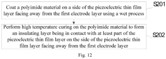
- step S103 an insulating layer in contact with at least part of the piezoelectric thin film layer is formed on a side of the piezoelectric thin film layer facing away from the first electrode layer, including:
- the implementation procedure for steps S201 to S202 is as follows: first, a wet process is employed, a side of the piezoelectric thin film layer 3 facing away from the first electrode layer 2 is coated with a polyimide material, in the case of cracks in the piezoelectric thin film layer 3, the polyimide material will flow through gravitational leveling into the cracks due to strong capillary forces and pores at the cracks, thereby ensuring insulating properties between the piezoelectric thin film layer 3 and the second electrode layer 5; then, the polyimide material is subjected to high temperature curing, an insulating layer 4 making contact with at least part of the piezoelectric thin film layer 3 is formed on the side of the piezoelectric thin film layer 3 facing away from the first electrode layer 2, for example, the polyimide material is cured at 200°C, thus ensuring that the insulating layer 4 has stable insulating properties and further ensuring the performance of the piezoelectric sensor.
- the principle of solving the problem with the fabrication method for the piezoelectric sensor described above is similar to that of the piezoelectric sensor described above, and therefore, the fabrication method for the piezoelectric sensor can refer to the implementation of the piezoelectric sensor section described above, and the repetition thereof will not be repeated.
- An embodiment of the present disclosure provides a piezoelectric sensor and a fabrication method, wherein the piezoelectric sensor includes the base substrate 1, and the first electrode layer 2, the piezoelectric thin film layer 3, the insulating layer 4 and the second electrode layer 5 which are arranged in sequence away from the base substrate 1, the insulating layer 4 is in contact with at least part of the piezoelectric thin film layer 3, even in the presence of cracks in the piezoelectric thin film layer 3, the cracks are filled by the insulating layer 4 effectively, so that the risk of short circuits between the second electrode layer 5 and the first electrode layer 2 due to contact, i.e. the risk of short circuits of the piezoelectric sensor, is avoided by the insulating layer 4 after deposition of the second electrode layer 5, thereby increasing the product yield.
Landscapes
- Engineering & Computer Science (AREA)
- General Engineering & Computer Science (AREA)
- Theoretical Computer Science (AREA)
- Physics & Mathematics (AREA)
- General Physics & Mathematics (AREA)
- Human Computer Interaction (AREA)
- Manufacturing & Machinery (AREA)
- Measurement Of Mechanical Vibrations Or Ultrasonic Waves (AREA)
- Piezo-Electric Or Mechanical Vibrators, Or Delay Or Filter Circuits (AREA)
- Measuring Fluid Pressure (AREA)
- Force Measurement Appropriate To Specific Purposes (AREA)
Abstract
Description
- The present disclosure relates to the field of sensor technology, in particular to a piezoelectric sensor, a fabrication method therefor, and a haptic feedback device.
- Haptic feedback (known as Haptics) is the focus of today's technology development, and in particular, haptic feedback enables the terminal to interact with the human body through touch. Haptic feedback, in turn, can be divided into two categories, one is vibration feedback and the other is tactile reproduction technology.
- The present disclosure provides a piezoelectric sensor, a fabrication method therefor, and a haptic feedback device. And, the solution is as follows.
- An embodiment of the present disclosure provides a piezoelectric sensor, including: a base substrate, and a first electrode layer, a piezoelectric thin film layer, an insulating layer, and a second electrode layer which are arranged in sequence away from the base substrate, where the insulating layer is in contact with at least part of the piezoelectric thin film layer.
- In some embodiments, a side of the piezoelectric thin film layer facing away from the base substrate includes at least one hollow structure, and each of the at least one hollow structures is filled with the insulating layer.
- In some embodiments, an orthographic projection of the piezoelectric thin film layer on the base substrate covers an orthographic projection of the insulating layer on the base substrate.
- In some embodiments, an orthographic projection of the insulating layer on the base substrate and an orthographic projection of the piezoelectric thin film layer on the base substrate overlap each other.
- In some embodiments, a material of the insulating layer includes at least one of polyimide, silica, or alumina.
- In some embodiments, a thickness of the insulating layer and a thickness of the piezoelectric thin film layer satisfy a following relationship:

- In some embodiments, a thickness of the insulating layer is greater than or equal to 50 nm; and the thickness of the insulating layer is less than or equal to 200 nm.
- In some embodiments, a thickness of the piezoelectric thin film layer is greater than 0; and the thickness of the piezoelectric thin film layer is less than or equal to 2µm.
- In some embodiments, a capacitance of the piezoelectric thin film layer and a capacitance of the insulating layer satisfy a following relationship:

- In some embodiments, a resistance of the piezoelectric thin film layer and a resistance of the insulating layer satisfy a following relationship:

- In some embodiments, a side of the piezoelectric thin film layer facing away from the base substrate is provided with a lyophilic material layer.
- In some embodiments, a material of the piezoelectric thin film layer includes at least one of aluminum nitride, zinc oxide, lead zirconate titanate, barium titanate, lead titanate, potassium niobate, lithium niobate, lithium tantalate, or lanthanum gallium silicate.
- In some embodiments, a side of the first electrode layer close to the piezoelectric thin film layer is provided with a plurality of first columnar structures.
- In some embodiments, a side of the second electrode layer facing the piezoelectric thin film layer is provided with a plurality of second columnar structures.
- In some embodiments, a side of the first electrode layer facing the piezoelectric thin film layer is provided with a plurality of third columnar structures, the side of the second electrode layer facing the piezoelectric thin film layer is provided with a plurality of fourth columnar structures, and an orthographic projection of each of the third columnar structures on the base substrate does not overlap with an orthographic projection of each of the fourth columnar structures on the base substrate.
- Accordingly, an embodiment of the present disclosure provides a haptic feedback device, including a haptic feedback circuit and a piezoelectric sensor as described in any one of the above; where:
- the haptic feedback circuit is arranged on a side of the second electrode layer facing away from the first electrode layer; or
- the haptic feedback circuit is arranged on a side of the first electrode layer facing away from the second electrode layer;
- where the haptic feedback circuit is configured to generate a voltage pulse in accordance with a received instruction to cause a structural body to vibrate.
- Accordingly, an embodiment of the present disclosure provides a fabrication method for a piezoelectric sensor, including:
- forming a first electrode layer on a base substrate;
- forming a piezoelectric thin film layer on a side of the first electrode layer facing away from the base substrate;
- forming an insulating layer being in contact with at least part of the piezoelectric thin film layer on a side of the piezoelectric thin film layer facing away from the first electrode layer; and
- forming a second electrode layer on a side of the insulating layer facing away from the piezoelectric thin film layer.
- In some embodiments, the forming the insulating layer being in contact with at least part of the piezoelectric thin film layer on the side of the piezoelectric thin film layer facing away from the first electrode layer, includes:
- coating a polyimide material on a side of the piezoelectric thin film layer facing away from the first electrode layer using a wet process; and
- performing high temperature curing on the polyimide material to form an insulating layer being in contact with at least part of the piezoelectric thin film layer on the side of the piezoelectric thin film layer facing away from the first electrode layer.
-
-
Fig. 1 is a schematic top view of a piezoelectric layer with cracks in a thin film vibration chip in the related art. -
Fig. 2 is a schematic structural diagram of a piezoelectric sensor according to an embodiment of the present disclosure. -
Fig. 3 is another schematic structural diagram of the piezoelectric sensor according to an embodiment of the present disclosure. -
Fig. 4 is another schematic structural diagram of the piezoelectric sensor according to an embodiment of the present disclosure. -
Fig. 5 is another schematic structural diagram of the piezoelectric sensor according to an embodiment of the present disclosure. -
Fig. 6 is another schematic structural diagram of the piezoelectric sensor according to an embodiment of the present disclosure. -
Fig. 7 is another schematic structural diagram of the piezoelectric sensor according to an embodiment of the present disclosure. -
Fig. 8 is another schematic structural diagram of the piezoelectric sensor according to an embodiment of the present disclosure. -
Fig. 9 is another schematic structural diagram of the piezoelectric sensor according to an embodiment of the present disclosure. -
Fig. 10 is a schematic structural diagram of a haptic feedback device according to an embodiment of the present disclosure. -
Fig. 11 is a method flow diagram of a fabrication method for the piezoelectric sensor according to an embodiment of the present disclosure. -
Fig. 12 is a method flowchart of step S103 inFig. 11 . - In order to make objectives, technical solutions and advantages of embodiments of the disclosure clearer, the technical solutions of embodiments of the disclosure are described clearly and completely below with reference to the drawings of embodiments of the disclosure. Apparently, the described embodiments are some, not all, of the embodiments of the disclosure. Embodiments in the disclosure and features in the embodiments may be mutually combined under the condition of no conflict. Based on the described embodiments of the disclosure, all other embodiments obtained by those ordinarily skilled in the art without creative work fall within the protection scope of the disclosure.
- Unless otherwise defined, technical or scientific terms used in the present disclosure shall have the ordinary meaning as understood by those of ordinary skill in the art to which this present disclosure belongs. The words "including," "comprising," and the like are used in this disclosure to mean that elements or items preceding the word appear to encompass elements or items listed after the word and equivalents thereof, without excluding other elements or items.
- The thin film piezoelectric material has the characteristics of high dielectric constant and transparency, and is well-suited for screen-integrated vibrator structures, when the surface charge distribution is uneven to lead accumulation or the voltage is too high, the vibrator undergoes breakdown phenomena, for example, the upper and lower electrodes remain open, but the piezoelectric thin film layer structure is damaged, and for another example, the upper and lower electrodes are short-circuited due to breakdown, resulting in failure of the entire vibrator. The main cause of short circuit is the stress of particles, granules or films in the process, which leads to cracks in the piezoelectric film layer. In this crack state, if the electrode is directly deposited on the piezoelectric film layer, it will lead to high short circuit risk. Therefore, how to avoid short circuit of the piezoelectric sensor has become an urgent technical problem to be solved.
- In the related art,
Fig. 1 is a schematic top view of a piezoelectric layer with cracks in a thin film vibration chip in the related art, during the process, the stress of particles, granules or films leads to cracks in the piezoelectric layer, and if the electrode is deposited directly on the piezoelectric layer, the cracks will lead to short circuit of the thin film vibration chip, thus reducing product yield. - In view of this, embodiments of the present disclosure provide a piezoelectric sensor, a fabrication method therefor, and a haptic feedback device for avoiding short circuits in the piezoelectric sensor and improving product yield.
-
Fig. 2 is a schematic structural diagram of a piezoelectric sensor according to an embodiment of the present disclosure, and the piezoelectric sensor, including: abase substrate 1, and afirst electrode layer 2, a piezoelectricthin film layer 3, aninsulating layer 4 and asecond electrode layer 5 which are arranged in sequence away from thebase substrate 1, where theinsulating layer 4 is in contact with at least part of the piezoelectricthin film layer 3. - In some embodiments, the
base substrate 1 can be a substrate made of glass, or silicon or silicon dioxide (SiO2), or sapphire, or metal wafer, which is not limited here, and the skilled person can set up thebase substrate 1 according to the needs of the actual application. - In some embodiments, the
first electrode layer 2 may be made of indium tin oxide (ITO), thefirst electrode layer 2 can also be made of indium zinc oxide (IZO), or one of titanium gold (Ti-Au) alloy, titanium aluminum titanium (Ti-Al-Ti) alloy, titanium molybdenum (TiMo) alloy, and in addition, thefirst electrode layer 2 may be made of one of titanium (Ti), gold (Au), silver (Ag), molybdenum (Mo), copper (Cu), tungsten (W), and chromium (Cr), and the skilled person can arrange thefirst electrode layer 2 according to the needs of the actual application, which is not limited here. Accordingly, thesecond electrode layer 5 may also be made of the same material as thefirst electrode layer 2, which is not described in detail here. - In some embodiments, a material of the piezoelectric
thin film layer 3 may include at least one of aluminum nitride (AIN), ZnO (zinc oxide), lead zirconate titanate (Pb (Zr, Ti)O3, PZT), barium titanate (BaTiO3), lead titanate (PbTiO3), potassium niobate (KNbO3), lithium niobate (LiNbO3), lithium tantalate (LiTaO3), or gallium lanthanum silicate (La3Ga5SiO14), in this way, the vibration characteristics of the piezoelectric sensor are guaranteed while at the same time the piezoelectric sensor is transparent, in particular the material from which the piezoelectricthin film layer 3 is made can be selected according to the actual usage needs of the person skilled in the art, which is not limited here. When the piezoelectricthin film layer 3 is made using PZT, the piezoelectric properties of the respective piezoelectric sensor are guaranteed since the PZT has a high electric coefficient, the respective piezoelectric sensor can be applied in a haptic feedback device, and the PZT has high light transmittance that does not affect the display quality of the display device when it is integrated into the display device. - The insulating
layer 4 between the piezoelectricthin film layer 3 and thesecond electrode layer 5 is in contact with at least part of the piezoelectricthin film layer 3, the insulatinglayer 4 may be in contact with all of the piezoelectricthin film layer 3, for example, the insulatinglayer 4 completely covers the side of the piezoelectricthin film layer 3 facing away from thebase substrate 1,Fig. 2 illustrates that the insulatinglayer 4 completely covers the side of the piezoelectricthin film layer 3 facing away from thebase substrate 1, and may also be in contact with a part of the piezoelectricthin film layer 3, for example, the insulatinglayer 4 fills only cracks in the piezoelectricthin film layer 3, for another example, the insulatinglayer 4 is disposed only within a portion of the area of the piezoelectricthin film layer 3 facing away from thebase substrate 1. - In some embodiments, the piezoelectric
thin film layer 3 may be arranged entirely on a side of thefirst electrode layer 2 facing away from thebase substrate 1, the efficiency of fabrication of the piezoelectric sensor is improved, and in addition, the piezoelectricthin film layer 3 can be patterned as needed, for example, the piezoelectricthin film layer 3 is arranged in areas on the side of thefirst electrode layer 2 facing away from thebase substrate 1, thereby enabling flexible design of the piezoelectric sensor. In some embodiments, since the insulatinglayer 4 is in contact with at least part of the piezoelectricthin film layer 3, even in the presence of cracks in the piezoelectricthin film layer 3, by means of the insulatinglayer 4 it is possible to effectively fill the cracks. Thus, after thesecond electrode layer 5 is deposited, the existence of the insulatinglayer 4 prevents the short circuit between thesecond electrode layer 5 and thefirst electrode layer 2 due to contact, thereby avoiding the short circuit risk of the piezoelectric sensor and improving the product yield. - In an embodiment of the present disclosure,
Fig. 3 is a schematic structural diagram of the piezoelectric sensor, the piezoelectricthin film layer 3 includes at least one hollow structure f on the side facing away from thebase substrate 1, each of the hollow structures f being filled with the insulatinglayer 4. There may be one or a plurality of hollow structures f, and the case of one hollow structure f is illustrated inFig. 3 , and of course there may be a plurality of hollow structures f, which is not limited herein. The hollow structure f may be a crack present in the piezoelectricthin film layer 3. When there are a plurality of the hollow structures f, the sizes of the hollow structures f may be unequal, the distribution of which may be randomly distributed according to actual process conditions. As shown inFig. 4 , the insulatinglayer 4 completely fills each of the hollow structures f, and the thickness of the insulatinglayer 4 filled in each of the hollow structures f is equal to the depth of the respective hollow structure f, both the thickness direction of the insulatinglayer 4 and the depth direction of the hollow structure f are in a direction perpendicular to the plane of thebase substrate 1, the term "equal" is not exactly equal, may be approximately equal, or roughly equal. As such, each of the hollow structures f in the piezoelectricthin film layer 3 is effectively filled by the insulatinglayer 4, thus avoiding the risk of short circuits of the piezoelectric sensor, moreover, since the insulatinglayer 4 completely fills each of the hollow structures f, when other parts of the insulatinglayer 4 completely cover the side of the piezoelectricthin film layer 3 facing away from thebase substrate 1 except for the part filled to each of the hollow structures f, the flush arrangement of the side of the piezoelectricthin film layer 3 away from thebase substrate 1 is realized, thus ensuring the structural stability of the piezoelectric sensor made later and improving the service performance of the piezoelectric sensor. - In an embodiment of the present disclosure, in connection with
Figs. 4 and 5 , the orthographic projection of the insulatinglayer 4 on thebase substrate 1 falls entirely within the area of the orthographic projection of the piezoelectricthin film layer 3 on thebase substrate 1. In some embodiments, the insulatinglayer 4 may be provided only in an area where the piezoelectricthin film layer 3 is prone to cracking, for example, provided only in the area where the hollow structure f is present, the insulatinglayer 4 may be filled only in the hollow structure f, it may also be partially filled in the hollow structure f, for example, the overall thickness of the piezoelectricthin film layer 3 in a direction perpendicular to the plane of thebase substrate 1 is b, the depth of the hollow structure f is c and the thickness of the insulatinglayer 4 in a direction perpendicular to the plane in which thebase substrate 1 lies is d, c ≤ b, d ≤ c, wherein b = c = d when the insulatinglayer 4 completely fills the hollow structure f, as shown inFig. 5 , and b = c, d < c when the insulatinglayer 4 partially fills the hollow structure f, as shown inFig. 6 . As such, the hollow structure f on the piezoelectricthin film layer 3 is filled by the insulatinglayer 4, avoiding the risk of short circuits of the piezoelectric sensor. - In an embodiment of the present disclosure, still with reference to
Fig. 3 , the orthographic projection of the insulatinglayer 4 on thebase substrate 1 and the orthographic projection of the piezoelectricthin film layer 3 on thebase substrate 1 overlap with each other. In some embodiments, the insulatinglayer 4 may completely cover the side of the piezoelectricthin film layer 3 facing away from thebase substrate 1, and even when the piezoelectricthin film layer 3 originally has cracks, the hollow structure f is effectively filled through the insulatinglayer 4, thus avoiding the short circuit risk of the piezoelectric sensor and improving the product yield. - In an embodiment of the present disclosure, the insulating
layer 4 includes at least one of polyimide (PI), silica (SiO2), alumina (Al2O3). In some embodiments, if the hollow structure f is present in the piezoelectricthin film layer 3, the hollow structure f tends to have strong capillary force and porosity, when a wet process is employed, the insulatinglayer 4 may flow through gravitational leveling into the hollow structure f, for example, when PI is coated on the side of the piezoelectricthin film layer 3 facing away from thebase substrate 1 using a wet process, since PI has better leveling properties at the surface of the piezoelectricthin film layer 3, PI may quickly level the hollow structure f, while ensuring surface planarity on the side of the piezoelectricthin film layer 3 facing away from thebase substrate 1 and avoiding the risk of short circuits of the piezoelectric sensor, since PI has the better high temperature curing (cyclization) property, after PI wet coating on the side of the piezoelectricthin film layer 3 facing away from thebase substrate 1, high temperature curing of PI within the range of 200°C ~ 300°C forms the insulatinglayer 4, thereby ensuring stable insulating properties of the insulatinglayer 4 and improving the performance of the piezoelectric sensor. - In some embodiments, SiO2 may also be coated on the side of the piezoelectric
thin film layer 3 facing away from thebase substrate 1 using a wet process, thereby leveling the hollow structure f, ensuring surface planarity on the side of the piezoelectricthin film layer 3 facing away from thebase substrate 1, and avoiding the risk of short circuits of the piezoelectric sensor, after SiO2 wet coating on the side of the piezoelectricthin film layer 3 facing away from thebase substrate 1, the insulatinglayer 4 is formed by high temperature curing of SiO2 at not less than 300°C, thereby ensuring stable insulating properties of the insulatinglayer 4 and improving the performance of the piezoelectric sensor. - In some embodiments, a dry deposition process may also be used to coat Al2O3 on the side of the piezoelectric
thin film layer 3 facing away from thebase substrate 1, avoiding the risk of short circuits of the piezoelectric sensor due to the insulation property of Al2O3 and further improving the performance of the piezoelectric sensor. Of course, the piezoelectricthin film layer 3 may be arranged in other ways and will not be described in detail herein. - In an embodiment of the present disclosure, the thickness of the insulating
layer 4 and the thickness of the piezoelectricthin film layer 3 satisfy the following relationship:
layer 4 and dPZT represents the thickness of the piezoelectricthin film layer 3. - In some embodiments, the inventors found in practical studies that, at a certain thickness of the piezoelectric
thin film layer 3, the thickness of the insulatinglayer 4 coated on a side of the piezoelectricthin film layer 3 facing away from thebase substrate 1 is set to be less than 10% of the thickness of the piezoelectricthin film layer 3, for example, when the thickness of the piezoelectricthin film layer 3 is 2 µm, the insulatinglayer 4 may have a thickness of 200 nm, it can be 100 nm or 50 nm, and is not limited herein, the insulating properties of the insulatinglayer 4 can be guaranteed, so that the risk of short circuits of the piezoelectric sensor is avoided and the vibration properties of the piezoelectric sensor during high frequency AC driving are guaranteed, thus improving the performance of the piezoelectric sensor. - In an embodiment of the present disclosure, a thickness of the insulating
layer 4 is greater than or equal to 50 nm; and the thickness of the insulatinglayer 4 is less than or equal to 200 nm. - In some embodiments, the insulating
layer 4 has a thickness between 50 nm and 200 nm, such as 100 nm, 60 nm, or 50 nm, the insulatinglayer 4 has better insulating properties when the thickness of the insulatinglayer 4 is in the above range, thus effectively avoiding the risk of short circuits of the piezoelectric sensor. - In an embodiment of the present disclosure, a thickness of the piezoelectric
thin film layer 3 is greater than 0; and the thickness of the piezoelectricthin film layer 3 is less than or equal to 2µm. - In some embodiments, the thickness of the piezoelectric
thin film layer 3 is between 0 ~ 2 µm, for example, the thickness of the piezoelectricthin film layer 3 is 0.5 µm, for another example, the thickness of the piezoelectricthin film layer 3 is 1 µm, and for another example, the thickness of the piezoelectricthin film layer 3 is 2 µm, and in practical applications, the thickness of the piezoelectricthin film layer 3 may be set as close to zero as possible, thus taking into account a lightly thinned design of the piezoelectric sensor while ensuring better vibration properties of the piezoelectricthin film layer 3. - In an embodiment of the present disclosure, a capacitance of the piezoelectric
thin film layer 3 and a capacitance of the insulatinglayer 4 satisfy the following relationship:
thin film layer 3 and CPZT represents the capacitance of the insulatinglayer 4. - In some embodiments, when the piezoelectric
thin film layer 3 is of a certain material, for instance, a film layer made of PbTiO3, and a thickness of the piezoelectricthin film layer 3 is fixed, an opposite area between thefirst electrode layer 2 and thesecond electrode layer 5 is fixed, from the capacitance calculation formula, the capacitance of the piezoelectricthin film layer 3 may be determined as:
thin film layer 3, which ranges from 450 ~ 1500, dPZT represents the thickness of the piezoelectricthin film layer 3, and A represents the opposite area between thefirst electrode layer 2 and thesecond electrode layer 5. - The capacitance of the piezoelectric
thin film layer 3 and the capacitance of the insulatinglayer 4 satisfies the relationship: CPI ≥ 100CPZT, the voltage loaded on the piezoelectricthin film layer 3 is:
thin film layer 3 by providing the insulatinglayer 4 on the surface of the piezoelectricthin film layer 3 facing away from thebase substrate 1 is avoided, which guarantees better vibration properties of the piezoelectric sensor under high frequency AC drive and performance of the piezoelectric sensor. Furthermore, when the capacitance of the piezoelectricthin film layer 3 is certain, according to the capacitance relationship between the piezoelectricthin film layer 3 and the insulatinglayer 4 described above, the material as well as the thickness of the insulatinglayer 4 is selected, the dielectric constant of the insulatinglayer 4 ranges from 2.3 ~ 2.8 when the insulatinglayer 4 is made of PI material, the insulatinglayer 4 can be arranged according to the circumstances of the piezoelectricthin film layer 3 in practical applications, thereby enabling flexible preparation of the piezoelectric sensor. - In an embodiment of the present disclosure, the resistance of the piezoelectric
thin film layer 3 and the resistance of the insulatinglayer 4 satisfy the following relationship:
thin film layer 3 and RPZT represents the resistance of the insulatinglayer 4. - In some embodiments, when the piezoelectric
thin film layer 3 is of a certain material, for instance, a film layer made of PbTiO3, and a thickness of the piezoelectricthin film layer 3 is fixed, a cross-sectional area of the piezoelectricthin film layer 3 parallel to a plane of thebase substrate 1 is fixed, according to the resistance calculation formula, the capacitance of the piezoelectricthin film layer 3 can be determined as:
thin film layer 3, which is greater than or equal to 109 Ωcm, dPZT represents the thickness of the piezoelectricthin film layer 3, A represents the cross-sectional area of the piezoelectricthin film layer 3 parallel to the plane of thebase substrate 1, which may be equal to the opposite area between thefirst electrode layer 2 and thesecond electrode layer 5. - When the resistance of the piezoelectric
thin film layer 3 and the resistance of the insulatinglayer 4 satisfies RPI ≥ 1000RPZT, the insulatinglayer 4 has better insulating properties, effectively avoiding the risk of short circuits of the piezoelectric sensor. When the resistance of the piezoelectricthin film layer 3 is certain, the material of the insulatinglayer 4 and the corresponding thickness range can be determined according to the resistance calculation formula, and the insulatinglayer 4 can be arranged according to the circumstances of the piezoelectricthin film layer 3 in practical applications, thereby enabling flexible preparation of the piezoelectric sensor. - In an embodiment of the present disclosure, the side of the piezoelectric
thin film layer 3 facing away from thebase substrate 1 is provided with a lyophilic material layer. The lyophilic material layer not only guarantee fast leveling of the insulatinglayer 4 on the side of the piezoelectricthin film layer 3 facing away from thebase substrate 1, but also has better high temperature curing properties, thus ensuring stable insulating properties of the insulatinglayer 4, and further improving the performance of the piezoelectric sensor. - In an embodiment of the present disclosure, the following four implementation forms can be used to provide the
first electrode layer 2 and thesecond electrode layer 5, the first implementation form is still shown in connection withFig. 2 , thefirst electrode layer 2 and thesecond electrode layer 5 are each a full plate-shaped structure, or at least one of thefirst electrode layer 2 and thesecond electrode layer 5 may also include a patterned design and the orthographic projection of thesecond electrode layer 5 on thesubstrate 1 falls entirely within the area of the orthographic projection of thefirst electrode layer 2 on thesubstrate 1. - In an embodiment of the present disclosure, a second implementation form is shown in
Fig. 6 , a plurality of firstcolumnar structures 10 are arranged on a side of thefirst electrode layer 2 close to the piezoelectricthin film layer 3, thesecond electrode layer 5 is a full plate-shaped structure, or thesecond electrode layer 5 may also include a patterned design, as such, while avoiding short circuits of the piezoelectric sensor by the insulatinglayer 4, by the plurality of firstcolumnar structures 10, the contact area between the piezoelectricthin film layer 3 and thefirst electrode layer 2 is increased, structural stability between the piezoelectricthin film layer 3 and thefirst electrode layer 2 is ensured and the performance of the piezoelectric sensor is improved. - In some embodiments, the sizes of the plurality of the first
columnar structures 10 are same, and the firstcolumnar structures 10 may be unequally spaced from each other, or equally spaced, and the distribution of the firstcolumnar structures 10 may be arranged according to the needs of the actual application without limitation. When the firstcolumnar structures 10 are equally spaced, uniformity of the transmission rate at each location of the piezoelectric sensor is guaranteed, which guarantees the performance of the piezoelectric sensor in use. - In an embodiment of the present disclosure, a third implementation form is shown in
Fig. 7 , thefirst electrode layer 2 is a full plate-shaped structure, or thefirst electrode layer 2 may include a patterned design, a side of thesecond electrode layer 5 close to the piezoelectricthin film layer 3 is provided with a plurality of secondcolumnar structures 20, as such, while avoiding short circuits of the piezoelectric sensor by the insulatinglayer 4, by the plurality of secondcolumnar structures 20, the contact area between the piezoelectricthin film layer 3 and thesecond electrode layer 5 is increased, structural stability between the piezoelectricthin film layer 3 and thesecond electrode layer 5 is ensured and the performance of the piezoelectric sensor is improved. - In some embodiments, the sizes of the plurality of the second
columnar structures 20 are same, and the secondcolumnar structures 20 may be unequally spaced from each other, or equally spaced, and the distribution of the secondcolumnar structures 20 may be arranged according to the needs of the actual application without limitation. When the secondcolumnar structures 20 are equally spaced, uniformity of the transmission rate at each location of the piezoelectric sensor is guaranteed, which guarantees the performance of the piezoelectric sensor in use. - In an embodiment of the present disclosure, a fourth implementation form is shown in
Fig. 8 , a side of thefirst electrode layer 2 close to the piezoelectricthin film layer 3 is provided with a plurality of thirdcolumnar structures 30, a side of thesecond electrode layer 5 close to the piezoelectricthin film layer 3 is provided with a plurality of fourthcolumnar structures 40, an orthographic projection of any one of the thirdcolumnar structures 30 on thebase substrate 1 and an orthographic projection of any one of the fourthcolumnar structures 40 on thebase substrate 1 do not overlap, the contact area between the piezoelectricthin film layer 3 and thefirst electrode layer 2 is increased by the plurality of thirdcolumnar structures 30, the contact area between the piezoelectricthin film layer 3 and thesecond electrode layer 5 is increased by the plurality of fourthcolumnar structures 40, thereby ensuring structural stability between the piezoelectricthin film layer 3 and thefirst electrode layer 2 as well as thesecond electrode layer 5, respectively, and improving the performance of the piezoelectric sensor. Furthermore, the orthographic projections of any one of the thirdcolumnar structures 30 and any one of the fourthcolumnar structures 40 on thesubstrate 1 do not overlap each other, for example, an orthographic projection of any one of the fourthcolumnar structures 40 on thebase substrate 1 falls entirely within an area of an orthographic projection of a spacing region between two adjacent thirdcolumnar structures 30 on thebase substrate 1. While taking into account the structural stability, the uniformity of the thickness of the piezoelectricthin film layer 3 is ensured, and the occurrence of easy breakdown at a thinner position due to the uneven thickness of the piezoelectricthin film layer 3 is avoided, thereby ensuring the service performance of the piezoelectric sensor. - In some embodiments, the sizes of the third
columnar structures 30 are same, the sizes of the fourthcolumnar structures 40 are same, the thirdcolumnar structures 30 can be unequally spaced or equally spaced from each other, the fourthcolumnar structures 40 can be unequally spaced or equally spaced from each other, The distribution of the thirdcolumnar structures 30 and the fourthcolumnar structures 40 may be specifically set according to practical application requirements and is not limited herein. When the thirdcolumnar structures 30 are equally spaced and the fourthcolumnar structures 40 are equally spaced, uniformity of light transmission at each location of the piezoelectric sensor is guaranteed, and use performance of the piezoelectric sensor is guaranteed. - Of course, the
first electrode layer 2 and thesecond electrode layer 5 may be provided in other ways according to actual needs in addition to the above four implementation forms in practical applications, which will not be described in detail here. - It should be noted that the thickness of the
first electrode layer 2 is between 50 nm and 500 nm and the thickness of thesecond electrode layer 5 is between 50 nm and 500 nm, for example, the thickness of thefirst electrode layer 2 is 200 nm and the thickness of thesecond electrode layer 5 is 150 nm, and that the thicknesses of thefirst electrode layer 2 and thesecond electrode layer 5 can be arranged in an implementation form according to the needs of the actual application, which is not limited here. As used herein, "same" is not exactly same, and can be approximately same, or roughly same. - In an embodiment of the present disclosure, as shown in
Fig. 9 , which is a schematic structural diagram of the piezoelectric sensor, in addition to the film layers mentioned above, the piezoelectric sensor may further include aprotective layer 6 disposed on the periphery of thefirst electrode layer 2, the piezoelectricthin film layer 3, the insulatinglayer 4, and thesecond electrode layer 5, and arouting layer 7 coupled by vias through theprotective layer 6. In some embodiments, with the used of the inverse piezoelectric effect, thefirst electrode layer 2 is grounded and a high frequency AC voltage signal (VAC) is applied to thesecond electrode layer 5, so that the high-frequency AC voltage signal is applied to the piezoelectricthin film layer 3 and the insulatinglayer 4, thereby generating high-frequency vibration. Laser can be used to measure vibration displacement, thereby ensuring the service performance of the piezoelectric sensor. The protective layer may be SiO2, silicon nitride (Si3N4) or the like and is not limited herein. Of course, the piezoelectric sensor can be provided with other film layers according to the practical application in addition to the various film layers mentioned above and the arrangement in the related art can be referred to in detail. - It should be noted that, in an embodiment of the present disclosure, for the
first electrode layer 2, the piezoelectricthin film layer 3, the insulatinglayer 4, thesecond electrode layer 5 that are stacked in sequence along thebase substrate 1, the areas of the orthographic projections of them on thebase substrate 1 tend to decrease, that is, an orthographic projection of thesecond electrode layer 5 on thebase substrate 1 falls entirely within the area of an orthographic projection of the insulatinglayer 4 on thebase substrate 1, the orthographic projection of the insulatinglayer 4 on thebase substrate 1 falls entirely within the area of the orthographic projection of the piezoelectricthin film layer 3 on thebase substrate 1 and the orthographic projection of the piezoelectricthin film layer 3 on thebase substrate 1 falls entirely within the area of the orthographic projection of thefirst electrode layer 2 on thebase substrate 1. In this way, the film layers have a segment difference with each other, on the one hand, the rapid leveling of each film layer in the wet process is ensured, on the other hand, the structural stability of the piezoelectric sensor is ensured, thereby improving the service performance of the piezoelectric sensor. Furthermore, the piezoelectric sensor can be applied in the fields of medical treatment, automotive electronics, motion tracking systems, and the like. It is especially suitable for the wearable equipment field, monitoring and treatment of in vitro or in vivo medical treatment, electronic skin of artificial intelligence and other fields. In particular, the piezoelectric sensor may be used in brake pads, keyboards, mobile terminals, gamepads, onboard vehicles, and the like that can generate vibration and mechanical characteristics. - Based on the same disclosed concept, as shown in
Fig. 10 , an embodiment of the present disclosure also provides a haptic feedback device including ahaptic feedback circuit 100 and thepiezoelectric sensor 200 as described above; where: thehaptic feedback circuit 100 is arranged on a side of thesecond electrode layer 5 facing away from thefirst electrode layer 2, or the haptic feedback circuit is arranged on a side of thefirst electrode layer 2 facing away from thesecond electrode layer 5, thehaptic feedback circuit 100 being configured to generate a voltage pulse according to a received instruction to vibrate the structural body. - In some embodiments, the
haptic feedback circuit 100 is arranged on a side of thefirst electrode layer 2 facing away from thesecond electrode layer 5 as illustrated inFig. 10 . For example, the haptic feedback device can be combined with a touch screen, and the touch position of the human body can be determined through the touch screen, thereby generating the corresponding vibration waveform, amplitude and frequency, and realizing human-computer interaction. For another example, it is also possible to multiplex the haptic feedback device as a piezoelectric body, and the touch position of the human body can be determined by the piezoelectric sensor, thereby generating the corresponding vibration waveform, amplitude and frequency, and realizing human-computer interaction. Of course, the tactile feedback device can also be applied in the fields of medical treatment, automotive electronics, motion tracking systems and the like according to actual needs, and will not be described in detail herein. - Furthermore, the principle of solving the problem with the haptic feedback device is similar to that of the aforementioned piezoelectric sensor, and therefore, the relevant structure of the
piezoelectric sensor 200 in the haptic feedback device can be referred to the implementation of the aforementionedpiezoelectric sensor 200, and the repetition is not repeated. - Based on the same disclosed concept, as illustrated in
Fig. 11 , an embodiment of the present disclosure also provides a fabrication method for a piezoelectric sensor, including: - S101: a first electrode layer is formed on a base substrate;
- S102: a piezoelectric thin film layer is formed on a side of the first electrode layer facing away from the base substrate;
- S103: an insulating layer in contact with at least part of the piezoelectric thin film layer is formed on a side of the piezoelectric thin film layer facing away from the first electrode layer;
- S104: a second electrode layer is formed on a side of the insulating layer facing away from the piezoelectric thin film layer.
- In some embodiments, the particular structure of the piezoelectric sensor in the fabrication method is the same as described in the previous section and is not described in detail herein. A specific implementation procedure for steps S101 to S103 is as follows: first, a first electrode layer 2 is formed on the base substrate 1, e.g., ITO is sputtered on the base substrate 1 and then the ITO is patterned by photolithography and etching to form the first electrode layer 2 in a desired pattern; then a piezoelectric thin film layer 3 is formed on the side of the first electrode layer 2 facing away from the base substrate 1, for example, the piezoelectric thin film layer 3 is deposited on the side of the first electrode layer 2 facing away from the base substrate 1, and then the piezoelectric thin film layer 3 is patterned by photolithography and etching to form the piezoelectric thin film layer 3 in a desired pattern; then an insulating layer 4 in contact with at least part of the piezoelectric thin film layer 3 is coated on a side of the piezoelectric thin film layer 3 facing away from the first electrode layer 2; the second electrode layer 5 is then formed on the side of the insulating layer 4 facing away from the piezoelectric thin film layer 3, for example, ITO is sputtered on the side of the insulating layer 4 facing away from the piezoelectric thin film layer 3, and the ITO is then patterned by photolithography and etching to form the second electrode layer 5 in the desired pattern.
- In an embodiment of the present disclosure, as illustrated in
Fig. 12 , step S103: an insulating layer in contact with at least part of the piezoelectric thin film layer is formed on a side of the piezoelectric thin film layer facing away from the first electrode layer, including: - S201: a polyimide material is coated on a side of the piezoelectric thin film layer facing away from the first electrode layer using a wet process;
- S202: high temperature curing is performed on the polyimide material to form an insulating layer being in contact with at least part of the piezoelectric thin film layer on the side of the piezoelectric thin film layer facing away from the first electrode layer.
- In some embodiments, the implementation procedure for steps S201 to S202 is as follows: first, a wet process is employed, a side of the piezoelectric
thin film layer 3 facing away from thefirst electrode layer 2 is coated with a polyimide material, in the case of cracks in the piezoelectricthin film layer 3, the polyimide material will flow through gravitational leveling into the cracks due to strong capillary forces and pores at the cracks, thereby ensuring insulating properties between the piezoelectricthin film layer 3 and thesecond electrode layer 5; then, the polyimide material is subjected to high temperature curing, an insulatinglayer 4 making contact with at least part of the piezoelectricthin film layer 3 is formed on the side of the piezoelectricthin film layer 3 facing away from thefirst electrode layer 2, for example, the polyimide material is cured at 200°C, thus ensuring that the insulatinglayer 4 has stable insulating properties and further ensuring the performance of the piezoelectric sensor. - In some embodiments, the principle of solving the problem with the fabrication method for the piezoelectric sensor described above is similar to that of the piezoelectric sensor described above, and therefore, the fabrication method for the piezoelectric sensor can refer to the implementation of the piezoelectric sensor section described above, and the repetition thereof will not be repeated.
- An embodiment of the present disclosure provides a piezoelectric sensor and a fabrication method, wherein the piezoelectric sensor includes the
base substrate 1, and thefirst electrode layer 2, the piezoelectricthin film layer 3, the insulatinglayer 4 and thesecond electrode layer 5 which are arranged in sequence away from thebase substrate 1, the insulatinglayer 4 is in contact with at least part of the piezoelectricthin film layer 3, even in the presence of cracks in the piezoelectricthin film layer 3, the cracks are filled by the insulatinglayer 4 effectively, so that the risk of short circuits between thesecond electrode layer 5 and thefirst electrode layer 2 due to contact, i.e. the risk of short circuits of the piezoelectric sensor, is avoided by the insulatinglayer 4 after deposition of thesecond electrode layer 5, thereby increasing the product yield. - Though the preferred embodiments of the disclosure are already described, those skilled in the art can make extra changes and modifications to these embodiments once they know a basic inventive concept. Therefore, the appended claims are intended to be constructed to include the preferred embodiments and all changes and modifications fall within the scope of the disclosure.
- Obviously, those skilled in the art can make various changes and modifications to the present disclosure without departing from the spirit and scope of the present disclosure. As such, provided that these modifications and variations of the present disclosure fall within the scope of the claims of the present disclosure and their equivalents, the present disclosure is also intended to cover such modifications and variations.
Claims (18)
- A piezoelectric sensor, comprising:a base substrate, anda first electrode layer, a piezoelectric thin film layer, an insulating layer, and a second electrode layer which are arranged in sequence away from the base substrate;wherein the insulating layer is in contact with at least part of the piezoelectric thin film layer.
- The piezoelectric sensor according to claim 1, wherein a side of the piezoelectric thin film layer facing away from the base substrate comprises at least one hollow structure, and each of the at least one hollow structure is filled with the insulating layer.
- The piezoelectric sensor according to any one of claims 1 to 2, wherein an orthographic projection of the piezoelectric thin film layer on the base substrate covers an orthographic projection of the insulating layer on the base substrate.
- The piezoelectric sensor according to any one of claims 1 to 2, wherein an orthographic projection of the insulating layer on the base substrate and an orthographic projection of the piezoelectric thin film layer on the base substrate overlap each other.
- The piezoelectric sensor according to any one of claims 1 to 4, wherein a material of the insulating layer comprises at least one of polyimide, silica, or alumina.
- The piezoelectric sensor according to any one of claims 1 to 5, wherein a thickness of the insulating layer and a thickness of the piezoelectric thin film layer satisfy a following relationship:

- The piezoelectric sensor according to any one of claims 1 to 6, wherein a thickness of the insulating layer is greater than or equal to 50 nm; and the thickness of the insulating layer is less than or equal to 200 nm.
- The piezoelectric sensor according to any one of claims 1 to 7, wherein a thickness of the piezoelectric thin film layer is greater than 0; and the thickness of the piezoelectric thin film layer is less than or equal to 2µm.
- The piezoelectric sensor according to any one of claims 1 to 8, wherein a capacitance of the piezoelectric thin film layer and a capacitance of the insulating layer satisfy a following relationship:

- The piezoelectric sensor according to any one of claims 1 to 9, wherein a resistance of the piezoelectric thin film layer and a resistance of the insulating layer satisfy a following relationship:

- The piezoelectric sensor according to any one of claims 1 to 10, wherein a side of the piezoelectric thin film layer facing away from the base substrate is provided with a lyophilic material layer.
- The piezoelectric sensor according to any one of claims 1 to 11, wherein a material of the piezoelectric thin film layer comprises at least one of aluminum nitride, zinc oxide, lead zirconate titanate, barium titanate, lead titanate, potassium niobate, lithium niobate, lithium tantalate, or lanthanum gallium silicate.
- The piezoelectric sensor according to any one of claims 1 to 12, wherein a side of the first electrode layer facing the piezoelectric thin film layer is provided with a plurality of first columnar structures.
- The piezoelectric sensor according to any one of claims 1 to 12, wherein a side of the second electrode layer facing the piezoelectric thin film layer is provided with a plurality of second columnar structures.
- The piezoelectric sensor according to any one of claims 1 to 12, wherein a side of the first electrode layer facing the piezoelectric thin film layer is provided with a plurality of third columnar structures;a side of the second electrode layer facing the piezoelectric thin film layer is provided with a plurality of fourth columnar structures; andan orthographic projection of each of the third columnar structures on the base substrate does not overlap with an orthographic projection of each of the fourth columnar structures on the base substrate.
- A haptic feedback device, comprising a haptic feedback circuit and the piezoelectric sensor according to any one of claims 1 to 15;wherein: the haptic feedback circuit is arranged on a side of the second electrode layer facing away from the first electrode layer; orthe haptic feedback circuit is arranged on a side of the first electrode layer facing away from the second electrode layer;wherein the haptic feedback circuit is configured to generate a voltage pulse in accordance with a received instruction to cause a structural body to vibrate.
- A fabrication method for a piezoelectric sensor, comprising:forming a first electrode layer on a base substrate;forming a piezoelectric thin film layer on a side of the first electrode layer facing away from the base substrate;forming an insulating layer being in contact with at least part of the piezoelectric thin film layer on a side of the piezoelectric thin film layer facing away from the first electrode layer; andforming a second electrode layer on a side of the insulating layer facing away from the piezoelectric thin film layer.
- The fabrication method for the piezoelectric sensor according to claim 17, wherein the forming the insulating layer being in contact with at least part of the piezoelectric thin film layer on the side of the piezoelectric thin film layer facing away from the first electrode layer, comprises:coating a polyimide material on a side of the piezoelectric thin film layer facing away from the first electrode layer using a wet process; andperforming high temperature curing on the polyimide material to form an insulating layer being in contact with at least part of the piezoelectric thin film layer on the side of the piezoelectric thin film layer facing away from the first electrode layer.
Applications Claiming Priority (1)
| Application Number | Priority Date | Filing Date | Title |
|---|---|---|---|
| PCT/CN2021/096891 WO2022246821A1 (en) | 2021-05-28 | 2021-05-28 | Piezoelectric sensor, fabrication method therefor, and haptic feedback device |
Publications (3)
| Publication Number | Publication Date |
|---|---|
| EP4206635A1 true EP4206635A1 (en) | 2023-07-05 |
| EP4206635A4 EP4206635A4 (en) | 2024-02-28 |
| EP4206635B1 EP4206635B1 (en) | 2026-05-06 |
Family
ID=84228381
Family Applications (1)
| Application Number | Title | Priority Date | Filing Date |
|---|---|---|---|
| EP21942395.1A Active EP4206635B1 (en) | 2021-05-28 | 2021-05-28 | Piezoelectric sensor and haptic feedback device |
Country Status (5)
| Country | Link |
|---|---|
| US (1) | US20240023448A1 (en) |
| EP (1) | EP4206635B1 (en) |
| JP (1) | JP7729516B2 (en) |
| CN (1) | CN115701319A (en) |
| WO (1) | WO2022246821A1 (en) |
Family Cites Families (17)
| Publication number | Priority date | Publication date | Assignee | Title |
|---|---|---|---|---|
| JP2000351212A (en) | 1999-06-11 | 2000-12-19 | Hitachi Koki Co Ltd | Piezoelectric element, piezoelectric actuator using the same, and ink jet printhead provided with the same |
| US6297579B1 (en) * | 2000-11-13 | 2001-10-02 | Sandia National Laboratories | Electron gun controlled smart structure |
| JP2003282989A (en) | 2002-01-15 | 2003-10-03 | Matsushita Electric Ind Co Ltd | Piezoelectric actuator, ink jet head having the same, and ink jet recording apparatus |
| SG186621A1 (en) | 2004-06-09 | 2013-01-30 | Nikon Corp | Substrate holding device, exposure apparatus having same, exposure method, method for producing device, and liquid repellent plate |
| JP4630998B2 (en) * | 2005-05-31 | 2011-02-09 | 独立行政法人産業技術総合研究所 | Speaker device or microphone device |
| JP2012166418A (en) | 2011-02-14 | 2012-09-06 | Seiko Epson Corp | Piezoelectric element |
| CN104221174A (en) | 2012-07-26 | 2014-12-17 | 株式会社村田制作所 | Ceramic electronic component and method for producing ceramic electronic component |
| JP6103068B2 (en) * | 2013-09-20 | 2017-03-29 | 株式会社村田製作所 | Piezoelectric sensor |
| WO2015077200A1 (en) * | 2013-11-21 | 2015-05-28 | 3M Innovative Properties Company | Multi-layer piezoelectric polymer film devices and methods |
| CN205919915U (en) * | 2016-08-25 | 2017-02-01 | 贝骨新材料科技(上海)有限公司 | Piezoelectric film sensor component |
| CN108267263A (en) * | 2018-01-25 | 2018-07-10 | 杨松 | Sense body and preparation method thereof |
| JP2019169518A (en) | 2018-03-22 | 2019-10-03 | 株式会社東海理化電機製作所 | Piezoelectric element and tactile display device |
| JP2019216165A (en) * | 2018-06-12 | 2019-12-19 | スタンレー電気株式会社 | Piezoelectric device, piezoelectric actuator, and manufacturing method of piezoelectric device |
| CN110875357B (en) | 2018-08-31 | 2022-05-24 | 京东方科技集团股份有限公司 | Pixel defining structure, display panel, preparation method of display panel and display device |
| KR102617510B1 (en) * | 2019-06-28 | 2023-12-22 | 후지필름 가부시키가이샤 | Polymer composite piezoelectric material and piezoelectric film |
| CN111916555B (en) * | 2020-07-14 | 2025-09-09 | 欧菲微电子(南昌)有限公司 | Piezoelectric composite film and preparation method thereof |
| CN112129432B (en) * | 2020-09-15 | 2025-08-19 | 中国科学院深圳先进技术研究院 | Piezoelectric sensor and preparation method thereof |
-
2021
- 2021-05-28 WO PCT/CN2021/096891 patent/WO2022246821A1/en not_active Ceased
- 2021-05-28 US US18/247,779 patent/US20240023448A1/en active Pending
- 2021-05-28 CN CN202180001322.6A patent/CN115701319A/en active Pending
- 2021-05-28 JP JP2023523582A patent/JP7729516B2/en active Active
- 2021-05-28 EP EP21942395.1A patent/EP4206635B1/en active Active
Also Published As
| Publication number | Publication date |
|---|---|
| JP7729516B2 (en) | 2025-08-26 |
| EP4206635A4 (en) | 2024-02-28 |
| JP2024521270A (en) | 2024-05-31 |
| EP4206635B1 (en) | 2026-05-06 |
| US20240023448A1 (en) | 2024-01-18 |
| CN115701319A (en) | 2023-02-07 |
| WO2022246821A1 (en) | 2022-12-01 |
Similar Documents
| Publication | Publication Date | Title |
|---|---|---|
| US11146233B2 (en) | Elastic wave device and manufacturing method therefor | |
| EP4163986B1 (en) | Piezoelectric sensor and haptics device | |
| US12395151B2 (en) | Acoustic wave device | |
| EP2940864B1 (en) | Piezoelectric component | |
| US10924083B2 (en) | Piezoelectric device and method for manufacturing piezoelectric device | |
| US10666221B2 (en) | Elastic wave device | |
| US11437974B2 (en) | Acoustic wave device | |
| EP4206635B1 (en) | Piezoelectric sensor and haptic feedback device | |
| CN119422327A (en) | Elastic wave device | |
| JP2009100367A (en) | Piezoelectric vibration device | |
| CN117203600A (en) | Piezoelectric sensor, its driving method and tactile feedback device | |
| CN100594567C (en) | Electronic component | |
| CN117412659A (en) | A tactile reproduction device, its manufacturing method and a tactile reproduction device | |
| US11239820B2 (en) | Acoustic wave device | |
| JPWO2006080341A1 (en) | Piezoelectric oscillation element and piezoelectric oscillation component using the same | |
| CN117136345A (en) | Tactile feedback substrate and tactile feedback device | |
| CN115454249B (en) | Piezoelectric element, piezoelectric vibrator, and electronic apparatus | |
| US20240431209A1 (en) | Tactile-feedback base board and tactile-feedback device | |
| US12506460B2 (en) | Acoustic wave device | |
| US20240367197A1 (en) | Piezoelectric actuator and haptics apparatus | |
| US10847472B2 (en) | Elastic wave device | |
| US20240276884A1 (en) | Piezoelectric device, vibration panel and haptic feedback apparatus | |
| WO2024186697A1 (en) | Elastic wave device | |
| WO2024186696A1 (en) | Elastic wave device | |
| CN115933865A (en) | Vibration panel and vibration device |
Legal Events
| Date | Code | Title | Description |
|---|---|---|---|
| STAA | Information on the status of an ep patent application or granted ep patent |
Free format text: STATUS: THE INTERNATIONAL PUBLICATION HAS BEEN MADE |
|
| PUAI | Public reference made under article 153(3) epc to a published international application that has entered the european phase |
Free format text: ORIGINAL CODE: 0009012 |
|
| STAA | Information on the status of an ep patent application or granted ep patent |
Free format text: STATUS: REQUEST FOR EXAMINATION WAS MADE |
|
| 17P | Request for examination filed |
Effective date: 20230328 |
|
| AK | Designated contracting states |
Kind code of ref document: A1 Designated state(s): AL AT BE BG CH CY CZ DE DK EE ES FI FR GB GR HR HU IE IS IT LI LT LU LV MC MK MT NL NO PL PT RO RS SE SI SK SM TR |
|
| A4 | Supplementary search report drawn up and despatched |
Effective date: 20240126 |
|
| RIC1 | Information provided on ipc code assigned before grant |
Ipc: H10N 30/01 20230101ALI20240122BHEP Ipc: H10N 30/30 20230101ALI20240122BHEP Ipc: G01L 1/16 20060101AFI20240122BHEP |
|
| DAV | Request for validation of the european patent (deleted) | ||
| DAX | Request for extension of the european patent (deleted) | ||
| STAA | Information on the status of an ep patent application or granted ep patent |
Free format text: STATUS: EXAMINATION IS IN PROGRESS |
|
| 17Q | First examination report despatched |
Effective date: 20250724 |
|
| GRAP | Despatch of communication of intention to grant a patent |
Free format text: ORIGINAL CODE: EPIDOSNIGR1 |
|
| STAA | Information on the status of an ep patent application or granted ep patent |
Free format text: STATUS: GRANT OF PATENT IS INTENDED |
|
| INTG | Intention to grant announced |
Effective date: 20260216 |
|
| GRAS | Grant fee paid |
Free format text: ORIGINAL CODE: EPIDOSNIGR3 |
|
| GRAA | (expected) grant |
Free format text: ORIGINAL CODE: 0009210 |
|
| STAA | Information on the status of an ep patent application or granted ep patent |
Free format text: STATUS: THE PATENT HAS BEEN GRANTED |