EP4205896A1 - Electric resistance spot welding device and method - Google Patents
Electric resistance spot welding device and method Download PDFInfo
- Publication number
- EP4205896A1 EP4205896A1 EP21881462.2A EP21881462A EP4205896A1 EP 4205896 A1 EP4205896 A1 EP 4205896A1 EP 21881462 A EP21881462 A EP 21881462A EP 4205896 A1 EP4205896 A1 EP 4205896A1
- Authority
- EP
- European Patent Office
- Prior art keywords
- contact surface
- electrode
- welding
- axis
- symmetry axis
- Prior art date
- Legal status (The legal status is an assumption and is not a legal conclusion. Google has not performed a legal analysis and makes no representation as to the accuracy of the status listed.)
- Granted
Links
Images




Classifications
-
- B—PERFORMING OPERATIONS; TRANSPORTING
- B23—MACHINE TOOLS; METAL-WORKING NOT OTHERWISE PROVIDED FOR
- B23K—SOLDERING OR UNSOLDERING; WELDING; CLADDING OR PLATING BY SOLDERING OR WELDING; CUTTING BY APPLYING HEAT LOCALLY, e.g. FLAME CUTTING; WORKING BY LASER BEAM
- B23K11/00—Resistance welding; Severing by resistance heating
- B23K11/10—Spot welding; Stitch welding
- B23K11/11—Spot welding
-
- B—PERFORMING OPERATIONS; TRANSPORTING
- B23—MACHINE TOOLS; METAL-WORKING NOT OTHERWISE PROVIDED FOR
- B23K—SOLDERING OR UNSOLDERING; WELDING; CLADDING OR PLATING BY SOLDERING OR WELDING; CUTTING BY APPLYING HEAT LOCALLY, e.g. FLAME CUTTING; WORKING BY LASER BEAM
- B23K11/00—Resistance welding; Severing by resistance heating
- B23K11/30—Features relating to electrodes
-
- B—PERFORMING OPERATIONS; TRANSPORTING
- B23—MACHINE TOOLS; METAL-WORKING NOT OTHERWISE PROVIDED FOR
- B23K—SOLDERING OR UNSOLDERING; WELDING; CLADDING OR PLATING BY SOLDERING OR WELDING; CUTTING BY APPLYING HEAT LOCALLY, e.g. FLAME CUTTING; WORKING BY LASER BEAM
- B23K11/00—Resistance welding; Severing by resistance heating
- B23K11/30—Features relating to electrodes
- B23K11/3009—Pressure electrodes
-
- B—PERFORMING OPERATIONS; TRANSPORTING
- B23—MACHINE TOOLS; METAL-WORKING NOT OTHERWISE PROVIDED FOR
- B23K—SOLDERING OR UNSOLDERING; WELDING; CLADDING OR PLATING BY SOLDERING OR WELDING; CUTTING BY APPLYING HEAT LOCALLY, e.g. FLAME CUTTING; WORKING BY LASER BEAM
- B23K11/00—Resistance welding; Severing by resistance heating
- B23K11/30—Features relating to electrodes
- B23K11/31—Electrode holders and actuating devices therefor
-
- B—PERFORMING OPERATIONS; TRANSPORTING
- B23—MACHINE TOOLS; METAL-WORKING NOT OTHERWISE PROVIDED FOR
- B23K—SOLDERING OR UNSOLDERING; WELDING; CLADDING OR PLATING BY SOLDERING OR WELDING; CUTTING BY APPLYING HEAT LOCALLY, e.g. FLAME CUTTING; WORKING BY LASER BEAM
- B23K11/00—Resistance welding; Severing by resistance heating
- B23K11/36—Auxiliary equipment
-
- B—PERFORMING OPERATIONS; TRANSPORTING
- B23—MACHINE TOOLS; METAL-WORKING NOT OTHERWISE PROVIDED FOR
- B23K—SOLDERING OR UNSOLDERING; WELDING; CLADDING OR PLATING BY SOLDERING OR WELDING; CUTTING BY APPLYING HEAT LOCALLY, e.g. FLAME CUTTING; WORKING BY LASER BEAM
- B23K2101/00—Articles made by soldering, welding or cutting
- B23K2101/18—Sheet panels
- B23K2101/185—Tailored blanks
Definitions
- the present application relates to the field of welding, in particular to a device and a method for resistance spot welding.
- Resistance spot welding is a connection mode having stable welding quality, high production efficiency, and being prone to mechanization and automation. It is widely applied in automobiles, rail trains, electronics, household appliances and other manufacturing fields. Compared with common double-sided single-spot welding, single-sided double-spot welding is especially suitable for welding large slabs having large thickness ratio due to high production efficiency since two welding spots can be simultaneously welded. Since the single-sided double-spot welding is single-sided welding and suitable for only welding conditions that can be completed on a single side, it is widely applied in welding for rail train bodies.
- a distal end and a proximal end of a nugget in welding spots generated using the single-sided double-spot welding have asymmetrical morphologies, that is, an end of the nugget proximal to two electrodes has large thickness, and an end of the nugget distal to the two electrodes is small thickness.
- the distal end of the nugget can withstand less pressure since it has smaller thickness.
- the present application provides a device for resistance spot welding capable of improving nugget quality, which may solve the problem that the nugget quality is affected due to asymmetrical morphologies of a distal end and a proximal end of a nugget.
- the present application further provides a method for resistance spot welding capable of improving nugget quality.
- the device for resistance spot welding includes a pair of electrodes located on a same welding surface of a to-be-welded assembly, where the to-be-welded assembly has a symmetry axis, the pair of electrodes are symmetrically arranged on two sides of the symmetry axis, an end of each electrode is provided with a special-shaped contact surface, and each special-shaped contact surface is shifted in a direction away from the symmetry axis relative to an electrode axis; where the special-shaped contact surface is used for shifting a current density centerline generated by the pair of electrodes in a direction away from the symmetry axis relative to the electrode axis, and/or for deflecting a current density of each electrode in a direction away from the welding surface within the to-be-welded assembly.
- the electrode includes an electrode tip and an electrode rod, an end of the electrode tip is detachably sleeved on an end of the electrode rod, another end of the electrode tip is provided with a boss, and an end surface of the boss is provided with the special-shaped contact surface.
- the special-shaped contact surface includes a first contact surface, and a geometric center of the first contact surface is located on a side of the electrode axis distal to the symmetry axis.
- the special-shaped contact surface further includes a second contact surface, the second contact surface is connected to a side of the first contact surface proximal to the symmetry axis, and an area of the first contact surface is larger than an area of the second contact surface.
- the first contact surface and the second contact surface are respectively arranged on two sides of the electrode axis, where the first contact surface is located on a side distal to the symmetry axis, and the second contact surface is located on a side proximal to the symmetry axis.
- a guiding part is arranged on a side of the boss proximal to the symmetry axis, and the guiding part is connected between the special-shaped contact surface and an outer wall of the electrode tip; and the guiding part is inclined relative to the electrode axis, and is used for guiding the current density centerline to skew or incline to a side distal to the symmetry axis relative to the electrode axis.
- an end of the electrode tip is provided with a fitting hole arranged axially, and an end of the electrode rod is provided with a connecting part coaxially inserted into the fitting hole.
- a side wall of the fitting hole is provided with a sliding groove
- a side wall of the connecting part is provided with a sliding block slidably fitted in the sliding groove
- the sliding groove and the sliding block are provided along the electrode axis.
- an end surface of the fitting hole is provided with a positioning groove
- an end of the connecting part is provided with a positioning boss coaxially fitted in the positioning groove; and another end of the connecting part is connected with a rod body.
- the device further includes a bottom plate and a spacer plate
- the to-be-welded assembly includes an upper welding plate and a lower welding plate
- the upper welding plate and the lower welding plate are laid between the spacer plate and the bottom plate; and a surface of the spacer plate backing toward the upper welding plate is the welding surface.
- a method for resistance spot welding is performed by the device for resistance spot welding.
- the method for resistance spot welding includes:
- the device for resistance spot welding includes a pair of electrodes located on the same welding surface of a to-be-welded assembly, where the to-be-welded assembly is provided with a symmetry axis, the pair of electrodes are symmetrically arranged on two sides of the symmetry axis, an end of each electrode is provided with a special-shaped contact surface, and each special-shaped contact surface is biased toward a direction departing the symmetry axis relative to an electrode axis; where the special-shaped contact surface is used for making a current density centerline generated by the pair of electrodes bias toward a direction departing the symmetry axis relative to the electrode axis, and/or for making a current density of each electrode deflect in a tendency away from the welding surface within the to-be-welded assembly.
- the device of the present application can change the current density state of the electrode in the to-be-welded assembly, to appropriately enhance the heat input of an end of the nugget distal to the symmetry axis, and appropriately weak the heat input of an end of the nugget proximal to the symmetry axis, so as to make the morphology of the nugget at distal end and proximal end relative to the symmetry axis symmetrical and uniform, and make the morphology and stress state of the nugget meet the mechanical performance requirements under load, thus improving welding quality.
- the method for resistance spot welding is performed by the device for resistance spot welding.
- the method for resistance spot welding includes: driving a pair of electrodes to travel in parallel along a symmetry axis of a to-be-welded assembly on a welding surface of the to-be-welded assembly, to make the pair of electrodes act on the to-be-welded assembly synchronously, and generate a nugget corresponding to a special-shaped contact surface of each electrode of the pair of electrodes in the to-be-welded assembly, where a pair of nuggets are provided symmetrically relative to the symmetry axis, and/or, for each nugget, the nugget cross-sectional area in a lower welding plate of the to-be-welded assembly is larger than the nugget cross-sectional area in an upper welding plate of the to-be-welded assembly.
- the method for resistance spot welding is performed by the device for resistance spot welding, and the method for resistance spot welding has all the advantages of the device for resistance spot welding, which are not repeated here.
- connection to and “connected” shall be understood broadly, for example, it may be either fixedly connected or detachably connected, or can be integrated; it may be either mechanically connected, or electrically connected; and it may be either directly connected, or indirectly connected through an intermediate medium.
- connection to and “connected” shall be understood broadly, for example, it may be either fixedly connected or detachably connected, or can be integrated; it may be either mechanically connected, or electrically connected; and it may be either directly connected, or indirectly connected through an intermediate medium.
- a first feature is "on” or “under” a second feature can refer to that the first feature is directly contacted with the second feature, or the first feature is indirectly contacted with the second feature through an intermediate medium.
- the first feature is "on”, “above” and “over” the second feature can refer to that the first feature is directly above or obliquely above the second feature, or simply refer to that the stage height of the first feature is higher than that of the second feature.
- the first feature is "under”, “below” or “beneath” the second feature can refer to that the first feature is directly below or obliquely below the second feature, or simply refer to that the stage height of the first feature is lower than that of the second feature.
- an embodiment of the present application provides a device for resistance spot welding, and provides a method for resistance spot welding based on the device for resistance spot welding.
- the device for resistance spot welding includes a pair of electrodes capable of travelling in parallel and simultaneously welding a welding surface of a to-be-welded assembly.
- the pair of electrodes are located on the same welding surface of the to-be-welded assembly, and can travel in parallel along the same welding direction for synchronous welding.
- Currents generated in a welding assembly under the action of the pair of electrodes can interact with each other, and a pair of nuggets 7 can be generated in the welding assembly by the pair of electrodes, and then single-sided double-resistance-spot welding process is applied to the to-be-welded assembly.
- the to-be-welded assembly has a symmetry axis 6, the pair of electrodes are symmetrically arranged on two sides of the symmetry axis 6, an end of each electrode is provided with a special-shaped contact surface 20, and each special-shaped contact surface 20 is shifted in a direction away from the symmetry axis 6 relative to an electrode axis 11.
- the special-shaped contact surface 20 is used for shifting a current density centerline 21 generated by a corresponding electrode in a direction away from the symmetry axis 6 relative to the electrode axis 11, and/or for deflecting a current density of each electrode in a direction away from the welding surface within the to-be-welded assembly.
- the device for resistance spot welding can change a current density state of the electrode in the to-be-welded assembly by a structure arrangement of the special-shaped contact surfaces 20 of the pair of electrodes, to appropriately enhance the heat input at an end of the nugget 7 distal to the symmetry axis 6 (that is, a distal end of the nugget 7), and appropriately weak the heat input at an end of the nugget 7 proximal to the symmetry axis 6 (that is, a proximal end of the nugget 7), both distal end and proximal end of the nugget 7 relative to the symmetry axis 6 have symmetrical and uniform morphologies, and the morphologies and stress state of the nugget 7 meets the mechanical performance requirements when a load is applied, thereby improving welding quality.
- the symmetry axis 6 is a perpendicular line through a midpoint of a line connecting two electrode axes 11 of the pair of electrodes, that is, it is ensured to arrange symmetrically the pair of electrodes relative to the symmetry axis 6.
- the device for resistance spot welding further includes a bottom plate 3 and a spacer plate 5.
- the to-be-welded assembly includes an upper welding plate 41 and a lower welding plate 42, and the upper welding plate 41 and the lower welding plate 42 are laid between the spacer plate 5 and the bottom plate 3. A surface of the spacer plate 5 backing toward the upper welding plate 41 is the welding surface.
- the bottom plate 3 is used for providing support and leveling for the to-be-welded assembly.
- the spacer plate 5 is preferable a metal plate.
- a resistance of the spacer plate 5 and a contact resistance between the spacer plate 5 and the upper welding plate 41 can be used to increase heat production in a spot welding process and promote formation and growth of the nugget 7; and on the other hand, the electrode and the welding assembly can be separated to reduce the conduction of heat from a welding center area to the special-shaped contact surface 20, and reduce heat dissipation on a side of the welding surface of the upper welding plate 41.
- the thickness of the upper welding plate 41 is smaller than the thickness of the lower welding plate 42 and the upper welding plate 41 and lower welding plate 42 welded together can form a tailor rolled blank.
- a cross-sectional area of a part of the nugget 7 formed at the lower welding plate 42 of the to-be-welded assembly is larger than a cross-sectional area of a part of the nugget 7 formed at the upper welding plated 41 of the to-be-welded assembly, which can avoid a shifting of the nugget 7 and improve the side penetration rate of the thinner upper welding plate 41, thereby further improving welding quality.
- the quality of the nugget 7 of a welding spot can be improved and the problem that the nugget 7 is shifted to a thicker side of the to-be-welded assembly can be solved.
- an original rule of larger current density at the proximal end of the nugget 7 and small current density at the distal end of the nugget 7 is changed to a rule of even distribution of current at the distal end and the proximal end of the nugget 7, thereby alleviating or eliminating a phenomenon of an asymmetric nugget 7 caused by concentrated current distribution near an inner side of the end surface of the electrode inside the to-be-welded assembly during single-sided double-spot welding, thereby improving qualities of the welding spot and reducing welding energy consumption.
- each electrode includes an electrode tip 2 and an electrode rod 1.
- An end of the electrode tip 2 is detachably sleeved on an end of the electrode rod 1, and the electrode tip 2 can be disassembled at any time as required to replace a suitable electrode tip 2, thereby improving the flexibility of welding operation.
- Another end of the electrode tip 2 is provided with a boss, and an end surface of the boss is provided with the special-shaped contact surface 20.
- a side of the boss proximal to the symmetry axis 6 is provided with a guiding part 25, and the guiding part 25 is connected between the special-shaped contact surface 20 and an outer wall of the electrode tip 2.
- the guiding part 25 is inclined relative to the electrode axis 11, and is used for guiding a current density centerline 21 to skew or incline toward a side distal to the symmetry axis 6 relative to the electrode axis 11.
- the special-shaped contact surface 20 is arranged on a side of an end surface of the electrode tip 2 away from the symmetry axis 6, the current is deflected and guided by the guiding part 25 during passing through the electrode tip 2, and the current density centerlines 21 of all currents are shifted toward a side away from the symmetry axis 6 relative to an axis of the electrode tip 2 (that is, the electrode axis 11), or the current is deflected and inclined inside the electrode tip 2, and thus the position where the current enters the to-be-welded assembly from the special-shaped contact surface 20 is shifted toward a side away from the symmetry axis 6 relative to a projected position of the electrode axis 11 on the to-be-welded assembly.
- the current distribution has a property of the current being more outside and less inside, and balances the current distribution being sparse outside and dense inside caused by the current deflection during single-sided double-spot welding, the contact surface between the upper welding plate 41 and the lower welding plates 42 of the welding assembly has a uniform current density, and the nugget 7 having a symmetrical structure is formed under the condition of uniform current density, and welding quality is improved.
- the guiding part 25 is preferably a stepped structure and/or an arc-shaped smooth transition surface structure.
- an end of the electrode tip 2 is provided with an axially disposed fitting hole 24, and an end of the electrode rod 1 is provided with a connecting part coaxially inserted into the fitting hole 24.
- a side wall of the fitting hole 24 is provided with a sliding groove 22
- a side wall of the connecting part 13 is provided with a sliding block 15 slidably fitted in the sliding groove 22, and the sliding groove 22 and the sliding block 15 are provided along the electrode axis 11.
- an end face of the fitting hole 24 is provided with a positioning groove 23, and an end of the connecting part 13 is provided with a positioning boss 14 coaxially fitted in the positioning groove 23; and another end of the connecting part 13 is connected with a rod body 12.
- the rod body 12 of the electrode rod 1 is provided with a through hole along the electrode axis 11, and auxiliary mechanisms such as circuit elements and wires in the electrode tip 2 can be led through the through hole of the rod body 12, to avoid interference with the welding process.
- the special-shaped contact surface 20 includes a first contact surface 201, and a geometric center of the first contact surface 201 is located on a side of the electrode axis 11 distal to the symmetry axis 6.
- the shifting arrangement of the first contact surface 201 can guide the current to shift in a direction away from the symmetry axis 6, to change an incident angle of the current, when entering the to-be-welded assembly, the current is prone to being deflected in a direction away from the symmetry axis 6, to balance the current density being sparse outside and dense inside caused by the current deflection near the symmetry axis 6 during single-sided double-spot welding. Therefore, the current density is uniformed, and effect of current deflection of single-sided double-spot welding on the nugget 7 is alleviated or eliminated.
- the special-shaped contact surface 20 further includes a second contact surface 202, the second contact surface 202 is connected to a side of the first contact surface 201 proximal to the symmetry axis 6, and the area of the first contact surface 201 is larger than the area of the second contact surface 202.
- the current distribution has a property of the current being more outside and less inside , and balances the current distribution being sparse outside and dense inside caused by the current deflection during single-sided double-spot welding, the contact surface between the upper welding plate 41 and the lower welding plates 42 has a uniform current density, and a nugget 7 having distal end and the proximal end with a symmetrical structure is formed under the condition of uniform current density.
- the above first contact surface 201 and the second contact surface 202s can be combined, and the first contact surface 201 and the second contact surface 202 are respectively arranged on two sides of the electrode axis 11, where the first contact surface 201 is located on a side distal to the symmetry axis 6, and the second contact surface 202 is located on a side proximal to the symmetry axis 6. Therefore, when entering the to-be-welded assembly, the current is prone to be deflected in a direction away from the symmetry axis 6, and the contact surface between the upper welding plate 41 and the lower welding plates 42 of the welding assembly has a uniform current density, which further ensures symmetry and uniform structure of the nugget 7.
- the first contact surface 201 and the second contact surface 202 may be circular planes, elliptical planes, polygonal planes or planes with zigzag contour lines.
- FIG. 10 and FIG. 11 show a schematic diagram of current density and a schematic diagram of a structure of the nugget 7 of a contrast electrode tip 2' for comparing with the electrode tip 2 described in the embodiments of the present application.
- the contrast electrode tip 2' when vertically incident current flows to a proximal end of the pair of electrodes, the current is relatively deflected due to the interaction of the pair of electrodes.
- the contrast electrode tip 2' is provided with no special-shaped contact surface 20, and no spacer plate 5 is laid between the to-be-welded assembly and the contrast electrode tip 2', the current density centerline generated by the contrast electrode tip 2' coincides with an axis of the contrast electrode tip 11', and the current density generated by the electrode at a contact surface of the upper welding plate 41 and the lower welding plate 42 of the welding assembly has uneven distribution. As shown in FIG.
- the structure of the electrode tip 2 described in the embodiments of the present application can alleviate or eliminate effects of current deflection inside the plate under the electrodes on the nugget 7 during single-sided double-spot welding, thereby alleviating or eliminating the asymmetric structure of the nugget 7 during single-sided double-spot welding. While the quality of welding spots is ensured, welding energy consumption is decreased, and cost reduction and efficiency increase of single-sided double-spot welding process is realized.
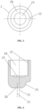
- FIG. 3, FIG. 4 and FIG. 5 show the structure of a first type of electrode tip 2.
- the special-shaped contact surface 20 of the first type of electrode tip 2 includes a first contact surface 201 and a second contact surface 202, and both the first contact surface 201 and the second contact surface 202 are semicircular planes and are provided on two sides of the electrode axis 11, respectively. That is, the centers of the first contact surface 201 and the second contact surface 202 coincide, and the radius of the first contact surface 201 is larger than the radius of the second contact surface 202, the area of the first contact surface 201 is larger than the area of the second contact surface 202.
- an outer wall of the boss between an outer contour of the second contact surface 202 and an outer wall of the electrode tip 2 is provided to be a guiding part 25 with a stepped structure and an arc-shaped smooth transition surface structure.
- an arc-shaped smooth transition surface structure is provided between an outer contour of the first contact surface 201 and the outer wall of the electrode tip 2.
- the first type of electrode tip 2 is preferably suitable for a to-be-welded assembly consisting of an upper welding plate 41 with a thickness of 0.8 mm and a lower welding plate 42 with a thickness of 2 mm, and the thickness of a metal spacer plate 5 is 0.1 mm.
- the radius of the first contact surface 201 is 8 mm, and the radius of the second contact surface 202 is 5.5 mm.
- the guiding part 25 is a stepped structure formed by removing 1 mm from the outer wall of the electrode tip 2 inward, and then connected to the outer contour of the second contact surface 202 through an arc-shaped smooth transition surface structure.
- the length of the electrode tip 2 is 13 mm, and the fitting hole 24 in the electrode tip 2 has a diameter of 12 mm and a length of 12 mm.
- a side wall of the fitting hole 24 is provided with a sliding groove 22 having a width of 2 mm and a length of 12 mm, and the shortest distance between the sliding groove 22 and the special-shaped contact surface 20 is 6.5 mm.
- a blind end of the fitting hole 24 is provided with a positioning groove 23 having a diameter of 8 mm and a length of 1 mm.
- FIG. 12 and FIG. 13 show a schematic diagram of the current density of the first type of electrode tip 2 and a schematic diagram of the structure of the nugget 7.
- the electrode tip 2 described in the embodiments can shift a current density centerline 21 in a direction away from the symmetry axis 6 relative to the electrode axis 11. Therefore, when entering the to-be-welded assembly, the current is prone to be deflected in a direction away from the symmetry axis 6, the position of the contact surface between the upper welding plate 41 and the lower welding plates 42 has a uniform current density, which further ensures symmetry and uniform structure of the nugget 7.
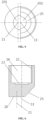
- FIG. 6 and FIG. 7 show the structure of a second type of electrode tip 2.
- the special-shaped contact surface 20 of the second type of electrode tip 2 has a first contact surface 201.
- the first contact surface 201 is a circular plane, and the center of the first contact surface 201 is located on a side of the electrode axis 11 away from the symmetry axis 6.
- an outer wall of the boss between an outer contour of the first contact surface 201 proximal to the symmetry axis 6 and an outer wall of the electrode tip 2 is provided to be a guiding part 25 with an arc-shaped smooth transition surface structure.
- the radius of the first contact surface 201 is 5 mm to 10 mm, and the distance between the center of the first contact surface 201 and the electrode axis 11 is 3 mm to 4 mm.
- the guiding part 25 is an arc-shaped smooth transition surface structure with an inclination angle of 35° to 45° from the outer wall of the electrode tip 2 and is connected with the outer contour of a side of the first contact surface 201 toward the symmetry axis 6.
- the sizes of the remaining structures of the second type of electrode tip 2 are the same as those of the first type of electrode tip 2.
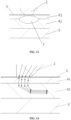
- FIG. 14 and FIG. 15 show a schematic diagram of the current density of the electrode tip 2 and a schematic diagram of the structure of the nugget 7.
- the electrode tip 2 described in the embodiments can shift a current density centerline 21 in a direction away from the symmetry axis 6 relative to the electrode axis 11. Therefore, when entering the to-be-welded assembly, the current is prone to being deflected in a direction away from the symmetry axis 6, and the position of the contact surface between the upper welding plate 41 and the lower welding plates 42 of the welding assembly has a uniform current density, which further ensures symmetry and uniform structure of the nugget 7.
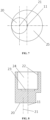
- FIG. 8 and FIG. 9 show the structure of a third type of electrode tip 2.
- the special-shaped contact surface 20 of the third type of electrode tip 2 includes a first contact surface 201 and a second contact surface 202, the first contact surface 201 and the second contact surface 202 are streamlined planes whose outer contour is formed by connecting two circular portions.
- the center of the first contact surface 201 is located on a side of the electrode axis 11 distal to the symmetry axis 6, and the center of the second contact surface 202 is located on the electrode axis 11.
- an outer wall of the boss between an outer contour of the first contact surface 201 proximal to the symmetry axis 6 and an outer wall of the electrode tip 2 is provided to be a guiding part 25 with a stepped structure.
- the radius of the first contact surface 201 is 5 mm
- the radius of the second contact surface 202 is 4 mm
- the distance between the center of the first contact surface 201 and the center of the second contact surface 202 is 3 mm.
- the length of the boss is 9 mm.
- the sizes of the remaining structures of the third type of electrode tip 2 are the same as those of the first type of electrode tip 2.
- the to-be-welded assemblies are placed on a copper bottom plate 3, and a metal gasket is covered on the upper welding plate 41 of the to-be-welded assembly; the positioning groove 23 inside the electrode tip 2 is then aligned and socketed with the positioning boss 14 at an end of the connecting part 13 of the electrode rod 1, and the contact surface with a larger area in the special-shaped contact surfaces 20 of each electrode tip 2 is located on a side distal to the symmetry axis 6; a pair of electrode tips 2 are driven subsequently to apply a constant electrode force through the spacer plate 5 to ensure the stability of the conductive path; a pair of electrode tips 2 are used to then apply current to the to-be-welded assembly and to heat up the inside of the to-be-welded assembly to form the nugget 7; and the pressure is maintained for a period of time after the power is turned off to cool the welding spots, and the single-sided double-spot welding process is completed.
- a method for resistance spot welding according to the embodiments of the present application is performed by the device for resistance spot welding.
- the method for resistance spot welding includes:
- the method for resistance spot welding is performed by the device for resistance spot welding, the method for resistance spot welding has all the advantages of the above device for resistance spot welding, which are not repeated here.
- electrode tips 2 of a pair of electrodes are replaced synchronously, to weld the to-be-welded assembly by using the electrode tips 2 with the most suitable structure of the special-shaped contact surface 20, so as to provide the optimal welding effect of single-sided double-spot welding.
Landscapes
- Engineering & Computer Science (AREA)
- Mechanical Engineering (AREA)
- Resistance Welding (AREA)
Abstract
Description
- The present application claims priority to
Chinese patent application No. 202011140736.0 filed on October 22, 2020 - The present application relates to the field of welding, in particular to a device and a method for resistance spot welding.
- Resistance spot welding is a connection mode having stable welding quality, high production efficiency, and being prone to mechanization and automation. It is widely applied in automobiles, rail trains, electronics, household appliances and other manufacturing fields. Compared with common double-sided single-spot welding, single-sided double-spot welding is especially suitable for welding large slabs having large thickness ratio due to high production efficiency since two welding spots can be simultaneously welded. Since the single-sided double-spot welding is single-sided welding and suitable for only welding conditions that can be completed on a single side, it is widely applied in welding for rail train bodies. However, in an actual production process, a distal end and a proximal end of a nugget in welding spots generated using the single-sided double-spot welding have asymmetrical morphologies, that is, an end of the nugget proximal to two electrodes has large thickness, and an end of the nugget distal to the two electrodes is small thickness. As such, when load is applied to the nugget, the distal end of the nugget can withstand less pressure since it has smaller thickness. In order to make the distal end of the nugget having a smaller thickness meet mechanical performance conditions, more welding heat input is required, resulting in the thickness of the nugget at the proximal end is greatly beyond demand, and even causing welding spatter on the distal end of nugget, which affects welding quality. In addition, welding quality is further affected due to nugget shift and insufficient penetration rate at a side having thin thickness when tailor rolled blanks are welded since the single-sided double-spot welding is commonly applied in the welding of tailor rolled blanks.
- The present application provides a device for resistance spot welding capable of improving nugget quality, which may solve the problem that the nugget quality is affected due to asymmetrical morphologies of a distal end and a proximal end of a nugget.
- The present application further provides a method for resistance spot welding capable of improving nugget quality.
- According to an embodiment of the present application, the device for resistance spot welding includes a pair of electrodes located on a same welding surface of a to-be-welded assembly, where the to-be-welded assembly has a symmetry axis, the pair of electrodes are symmetrically arranged on two sides of the symmetry axis, an end of each electrode is provided with a special-shaped contact surface, and each special-shaped contact surface is shifted in a direction away from the symmetry axis relative to an electrode axis;
where the special-shaped contact surface is used for shifting a current density centerline generated by the pair of electrodes in a direction away from the symmetry axis relative to the electrode axis, and/or for deflecting a current density of each electrode in a direction away from the welding surface within the to-be-welded assembly. - According to an embodiment of the present application, the electrode includes an electrode tip and an electrode rod, an end of the electrode tip is detachably sleeved on an end of the electrode rod, another end of the electrode tip is provided with a boss, and an end surface of the boss is provided with the special-shaped contact surface.
- According to an embodiment of the present application, the special-shaped contact surface includes a first contact surface, and a geometric center of the first contact surface is located on a side of the electrode axis distal to the symmetry axis.
- According to an embodiment of the present application, the special-shaped contact surface further includes a second contact surface, the second contact surface is connected to a side of the first contact surface proximal to the symmetry axis, and an area of the first contact surface is larger than an area of the second contact surface.
- According to an embodiment of the present application, the first contact surface and the second contact surface are respectively arranged on two sides of the electrode axis, where the first contact surface is located on a side distal to the symmetry axis, and the second contact surface is located on a side proximal to the symmetry axis.
- According to an embodiment of the present application, a guiding part is arranged on a side of the boss proximal to the symmetry axis, and the guiding part is connected between the special-shaped contact surface and an outer wall of the electrode tip; and the guiding part is inclined relative to the electrode axis, and is used for guiding the current density centerline to skew or incline to a side distal to the symmetry axis relative to the electrode axis.
- According to an embodiment of the present application, an end of the electrode tip is provided with a fitting hole arranged axially, and an end of the electrode rod is provided with a connecting part coaxially inserted into the fitting hole.
- According to an embodiment of the present application, a side wall of the fitting hole is provided with a sliding groove, a side wall of the connecting part is provided with a sliding block slidably fitted in the sliding groove, and the sliding groove and the sliding block are provided along the electrode axis.
- According to an embodiment of the present application, an end surface of the fitting hole is provided with a positioning groove, and an end of the connecting part is provided with a positioning boss coaxially fitted in the positioning groove; and another end of the connecting part is connected with a rod body.
- According to an embodiment of the present application, the device further includes a bottom plate and a spacer plate, the to-be-welded assembly includes an upper welding plate and a lower welding plate, and the upper welding plate and the lower welding plate are laid between the spacer plate and the bottom plate; and a surface of the spacer plate backing toward the upper welding plate is the welding surface.
- According to another aspect of the embodiments of the present application, a method for resistance spot welding is performed by the device for resistance spot welding. The method for resistance spot welding includes:
- driving a pair of electrodes to travel in parallel along a symmetry axis of a to-be-welded assembly on a welding surface of the to-be-welded assembly, to make the pair of electrodes act on the to-be-welded assembly synchronously, and generate a nugget corresponding to a special-shaped contact surface of each electrode of the pair of electrodes in the to-be-welded assembly;
- where a pair of nuggets are provided symmetrically relative to the symmetry axis, and/or, in each nugget, a nugget cross-sectional area in a lower welding plate of the to-be-welded assembly is larger than the nugget cross-sectional area in an upper welding plate of the to-be-welded assembly.
- The above one or more solutions in the embodiments of the present application have one or more of the following effects.
- The device for resistance spot welding according to the embodiment of the present application includes a pair of electrodes located on the same welding surface of a to-be-welded assembly, where the to-be-welded assembly is provided with a symmetry axis, the pair of electrodes are symmetrically arranged on two sides of the symmetry axis, an end of each electrode is provided with a special-shaped contact surface, and each special-shaped contact surface is biased toward a direction departing the symmetry axis relative to an electrode axis; where the special-shaped contact surface is used for making a current density centerline generated by the pair of electrodes bias toward a direction departing the symmetry axis relative to the electrode axis, and/or for making a current density of each electrode deflect in a tendency away from the welding surface within the to-be-welded assembly. The device of the present application can change the current density state of the electrode in the to-be-welded assembly, to appropriately enhance the heat input of an end of the nugget distal to the symmetry axis, and appropriately weak the heat input of an end of the nugget proximal to the symmetry axis, so as to make the morphology of the nugget at distal end and proximal end relative to the symmetry axis symmetrical and uniform, and make the morphology and stress state of the nugget meet the mechanical performance requirements under load, thus improving welding quality.
- The method for resistance spot welding according to the embodiments of the present application is performed by the device for resistance spot welding. The method for resistance spot welding includes: driving a pair of electrodes to travel in parallel along a symmetry axis of a to-be-welded assembly on a welding surface of the to-be-welded assembly, to make the pair of electrodes act on the to-be-welded assembly synchronously, and generate a nugget corresponding to a special-shaped contact surface of each electrode of the pair of electrodes in the to-be-welded assembly, where a pair of nuggets are provided symmetrically relative to the symmetry axis, and/or, for each nugget, the nugget cross-sectional area in a lower welding plate of the to-be-welded assembly is larger than the nugget cross-sectional area in an upper welding plate of the to-be-welded assembly. The method for resistance spot welding is performed by the device for resistance spot welding, and the method for resistance spot welding has all the advantages of the device for resistance spot welding, which are not repeated here.
- Additional aspects and advantages of the present application are set forth, and in part, from the following description, the part would become clear from the following description, or be learned by practice of the present application.
- In order to more clearly illustrate the solutions disclosed in the embodiments of the present application, the drawings used in the descriptions of the embodiments or the related art are briefly described below. The drawings in the following description are only of certain embodiments of the present application, and other drawings may be obtained according to these drawings without any creative efforts for those skilled in the art.
-
FIG. 1 is a schematic diagram showing a welding principle of a device for resistance spot welding according to an embodiment of the present application; -
FIG. 2 is a schematic diagram showing a welding principle of an electrode tip according to an embodiment of the present application; -
FIG. 3 is a top view of a first structure of an electrode tip according to an embodiment of the present application; -
FIG. 4 is a cross-sectional view of the first structure of an electrode tip according to an embodiment of the present application; -
FIG. 5 is a bottom view of the first structure of an electrode tip according to an embodiment of the present application; -
FIG. 6 is a cross-sectional view of a second structure of an electrode tip according to an embodiment of the present application; -
FIG. 7 is a bottom view of the second structure of an electrode tip according to an embodiment of the present application; -
FIG. 8 is a cross-sectional view of a third structure of an electrode tip according to an embodiment of the present application; -
FIG. 9 is a bottom view of the third structure of an electrode tip according to an embodiment of the present application; -
FIG. 10 is a schematic diagram of a current density of a contrast electrode tip according to an embodiment of the present application; -
FIG. 11 is a schematic diagram of a structure of a nugget of a contrast electrode tip according to an embodiment of the present application; -
FIG. 12 is a schematic diagram of a current density of a first structure of an electrode tip according to an embodiment of the present application; -
FIG. 13 is a schematic diagram of a nugget structure of the first structure of an electrode tip according to an embodiment of the present application; -
FIG. 14 is a schematic diagram of a current density of a second structure of an electrode tip according to an embodiment of the present application; -
FIG. 15 is a schematic diagram of a nugget structure of the second structure of an electrode tip according to an embodiment of the present application; -
FIG. 16 is a front view of an electrode rod according to an embodiment of the present application; and -
FIG. 17 is a bottom view of the electrode rod according to an embodiment of the present application. -
- 1: electrode rod; 11: electrode axis; 12: rod body; 13: connecting part; 14: positioning boss; 15: sliding block;
- 2: electrode tip; 20: special-shaped contact surface; 201: first contact surface; 202: second contact surface; 21: current density centerline; 22: sliding groove; 23: positioning groove; 24: fitting hole; 25: guiding part;
- 2': contrast electrode tip; 11': axis of the contrast electrode tip; 7': nugget;
- 3: bottom plate; 41: upper welding plate; 42: lower welding plate; 5: spacer plate; 6: symmetry axis; 7: nugget.
- The implementation of the present application is further described in detail below in combination with the accompanying drawings and embodiments. The following embodiments are used for describing the present application, but cannot be used for limiting the scope of the present application.
- In the description of the present application, it should be noted that, the orientation or positional relations specified by terms such as "central", "longitudinal", "transverse", "upper", "lower", "front", "rear", "left", "right", "vertical", "horizontal", "top", "bottom", "inner", "outer" and the like, are based on the orientation or positional relations shown in the drawings, which are merely for convenience of description of the present application and to simplify description, but do not indicate or imply that the stated devices or members must have the particular orientation and be constructed and operated in a particular orientation, and thus these can not to be construed as limiting the present application. Furthermore, the terms "first", "second", "third" and the like are only used for descriptive purposes and should not be construed as indicating or implying a relative importance.
- In the description of the present application, it should be noted that unless explicitly specified and defined otherwise, the terms "connected to" and "connected" shall be understood broadly, for example, it may be either fixedly connected or detachably connected, or can be integrated; it may be either mechanically connected, or electrically connected; and it may be either directly connected, or indirectly connected through an intermediate medium. The specific meanings of the terms above in the present application can be understood by those skilled in the art in accordance with specific conditions.
- In the embodiments of the present application, unless otherwise expressly specified and defined, a first feature is "on" or "under" a second feature can refer to that the first feature is directly contacted with the second feature, or the first feature is indirectly contacted with the second feature through an intermediate medium. And further, the first feature is "on", "above" and "over" the second feature can refer to that the first feature is directly above or obliquely above the second feature, or simply refer to that the stage height of the first feature is higher than that of the second feature. The first feature is "under", "below" or "beneath" the second feature can refer to that the first feature is directly below or obliquely below the second feature, or simply refer to that the stage height of the first feature is lower than that of the second feature.
- In the description of this specification, description with reference to the terms "one embodiment", "some embodiments", "an example", "specific example", "some examples" and the like, refers to that specific features, structures, materials or characteristics described in combination with an embodiment or an example are included in at least one embodiment or example according to the embodiments of the present application. In the present specification, schematic representations of the above terms are not necessarily directed to a same embodiment or example. Furthermore, the particular features, structures, materials or characteristics described can be combined in any suitable manner in any one or more embodiments or examples. In addition, those skilled in the art may combine the different embodiments or examples, as well as the features of the different embodiments or examples described in this specification, without conflicting each other.
- As shown in
FIG. 1 to FIG. 17 , an embodiment of the present application provides a device for resistance spot welding, and provides a method for resistance spot welding based on the device for resistance spot welding. - As shown in
FIG. 1 and FIG. 2 , the device for resistance spot welding includes a pair of electrodes capable of travelling in parallel and simultaneously welding a welding surface of a to-be-welded assembly. The pair of electrodes are located on the same welding surface of the to-be-welded assembly, and can travel in parallel along the same welding direction for synchronous welding. Currents generated in a welding assembly under the action of the pair of electrodes can interact with each other, and a pair ofnuggets 7 can be generated in the welding assembly by the pair of electrodes, and then single-sided double-resistance-spot welding process is applied to the to-be-welded assembly. - The to-be-welded assembly has a
symmetry axis 6, the pair of electrodes are symmetrically arranged on two sides of thesymmetry axis 6, an end of each electrode is provided with a special-shapedcontact surface 20, and each special-shapedcontact surface 20 is shifted in a direction away from thesymmetry axis 6 relative to anelectrode axis 11. The special-shapedcontact surface 20 is used for shifting acurrent density centerline 21 generated by a corresponding electrode in a direction away from thesymmetry axis 6 relative to theelectrode axis 11, and/or for deflecting a current density of each electrode in a direction away from the welding surface within the to-be-welded assembly. The device for resistance spot welding can change a current density state of the electrode in the to-be-welded assembly by a structure arrangement of the special-shaped contact surfaces 20 of the pair of electrodes, to appropriately enhance the heat input at an end of thenugget 7 distal to the symmetry axis 6 (that is, a distal end of the nugget 7), and appropriately weak the heat input at an end of thenugget 7 proximal to the symmetry axis 6 (that is, a proximal end of the nugget 7), both distal end and proximal end of thenugget 7 relative to thesymmetry axis 6 have symmetrical and uniform morphologies, and the morphologies and stress state of thenugget 7 meets the mechanical performance requirements when a load is applied, thereby improving welding quality. - The
symmetry axis 6 is a perpendicular line through a midpoint of a line connecting twoelectrode axes 11 of the pair of electrodes, that is, it is ensured to arrange symmetrically the pair of electrodes relative to thesymmetry axis 6. - For further improving the welding quality of single-sided double-spot welding, the device for resistance spot welding further includes a
bottom plate 3 and aspacer plate 5. The to-be-welded assembly includes anupper welding plate 41 and alower welding plate 42, and theupper welding plate 41 and thelower welding plate 42 are laid between thespacer plate 5 and thebottom plate 3. A surface of thespacer plate 5 backing toward theupper welding plate 41 is the welding surface. Thebottom plate 3 is used for providing support and leveling for the to-be-welded assembly. Thespacer plate 5 is preferable a metal plate. By additionally arranging thespacer plate 5 on a surface of the thinnerupper welding plate 41, on the one hand, a resistance of thespacer plate 5 and a contact resistance between thespacer plate 5 and theupper welding plate 41 can be used to increase heat production in a spot welding process and promote formation and growth of thenugget 7; and on the other hand, the electrode and the welding assembly can be separated to reduce the conduction of heat from a welding center area to the special-shapedcontact surface 20, and reduce heat dissipation on a side of the welding surface of theupper welding plate 41. - The thickness of the
upper welding plate 41 is smaller than the thickness of thelower welding plate 42 and theupper welding plate 41 andlower welding plate 42 welded together can form a tailor rolled blank. - After the current density of each electrode is deflected in a direction away from the welding surface within the to-be-welded assembly, a cross-sectional area of a part of the
nugget 7 formed at thelower welding plate 42 of the to-be-welded assembly is larger than a cross-sectional area of a part of thenugget 7 formed at the upper welding plated 41 of the to-be-welded assembly, which can avoid a shifting of thenugget 7 and improve the side penetration rate of the thinnerupper welding plate 41, thereby further improving welding quality. - During a single-sided double-point welding process of the tailor rolled blank using the device for resistance spot welding, the quality of the
nugget 7 of a welding spot can be improved and the problem that thenugget 7 is shifted to a thicker side of the to-be-welded assembly can be solved. By a structure arrangement of the special-shaped contact surfaces 20 at end surfaces of electrodes, an original rule of larger current density at the proximal end of thenugget 7 and small current density at the distal end of thenugget 7 is changed to a rule of even distribution of current at the distal end and the proximal end of thenugget 7, thereby alleviating or eliminating a phenomenon of anasymmetric nugget 7 caused by concentrated current distribution near an inner side of the end surface of the electrode inside the to-be-welded assembly during single-sided double-spot welding, thereby improving qualities of the welding spot and reducing welding energy consumption. - As shown in
FIG. 2 ,FIG. 3 ,FIG. 16 and FIG. 17 , each electrode includes anelectrode tip 2 and anelectrode rod 1. An end of theelectrode tip 2 is detachably sleeved on an end of theelectrode rod 1, and theelectrode tip 2 can be disassembled at any time as required to replace asuitable electrode tip 2, thereby improving the flexibility of welding operation. Another end of theelectrode tip 2 is provided with a boss, and an end surface of the boss is provided with the special-shapedcontact surface 20. Preferably, a side of the boss proximal to thesymmetry axis 6 is provided with a guidingpart 25, and the guidingpart 25 is connected between the special-shapedcontact surface 20 and an outer wall of theelectrode tip 2. The guidingpart 25 is inclined relative to theelectrode axis 11, and is used for guiding acurrent density centerline 21 to skew or incline toward a side distal to thesymmetry axis 6 relative to theelectrode axis 11. By the guidingpart 25, the special-shapedcontact surface 20 is arranged on a side of an end surface of theelectrode tip 2 away from thesymmetry axis 6, the current is deflected and guided by the guidingpart 25 during passing through theelectrode tip 2, and thecurrent density centerlines 21 of all currents are shifted toward a side away from thesymmetry axis 6 relative to an axis of the electrode tip 2 (that is, the electrode axis 11), or the current is deflected and inclined inside theelectrode tip 2, and thus the position where the current enters the to-be-welded assembly from the special-shapedcontact surface 20 is shifted toward a side away from thesymmetry axis 6 relative to a projected position of theelectrode axis 11 on the to-be-welded assembly. By the above structure, the current distribution has a property of the current being more outside and less inside, and balances the current distribution being sparse outside and dense inside caused by the current deflection during single-sided double-spot welding, the contact surface between theupper welding plate 41 and thelower welding plates 42 of the welding assembly has a uniform current density, and thenugget 7 having a symmetrical structure is formed under the condition of uniform current density, and welding quality is improved. - The guiding
part 25 is preferably a stepped structure and/or an arc-shaped smooth transition surface structure. - In order to flexibly assemble and disassemble the
electrode tip 2 and theelectrode rod 1, an end of theelectrode tip 2 is provided with an axially disposed fittinghole 24, and an end of theelectrode rod 1 is provided with a connecting part coaxially inserted into thefitting hole 24. In order to circumferentially position theelectrode tip 2 and theelectrode rod 1, a side wall of thefitting hole 24 is provided with a slidinggroove 22, a side wall of the connectingpart 13 is provided with a slidingblock 15 slidably fitted in the slidinggroove 22, and the slidinggroove 22 and the slidingblock 15 are provided along theelectrode axis 11. In order to radially and centrally position theelectrode tip 2 and theelectrode rod 1, an end face of thefitting hole 24 is provided with apositioning groove 23, and an end of the connectingpart 13 is provided with apositioning boss 14 coaxially fitted in thepositioning groove 23; and another end of the connectingpart 13 is connected with arod body 12. - The
rod body 12 of theelectrode rod 1 is provided with a through hole along theelectrode axis 11, and auxiliary mechanisms such as circuit elements and wires in theelectrode tip 2 can be led through the through hole of therod body 12, to avoid interference with the welding process. - In some embodiments, in order to reliably control the distribution of current density, the special-shaped
contact surface 20 includes afirst contact surface 201, and a geometric center of thefirst contact surface 201 is located on a side of theelectrode axis 11 distal to thesymmetry axis 6. During the process of the current flowing from theelectrode tip 2 and passing through thefirst contact surface 201 into the to-be-welded assembly with thespacer plate 5, the shifting arrangement of thefirst contact surface 201 can guide the current to shift in a direction away from thesymmetry axis 6, to change an incident angle of the current, when entering the to-be-welded assembly, the current is prone to being deflected in a direction away from thesymmetry axis 6, to balance the current density being sparse outside and dense inside caused by the current deflection near thesymmetry axis 6 during single-sided double-spot welding. Therefore, the current density is uniformed, and effect of current deflection of single-sided double-spot welding on thenugget 7 is alleviated or eliminated. - In some embodiments, the special-shaped
contact surface 20 further includes asecond contact surface 202, thesecond contact surface 202 is connected to a side of thefirst contact surface 201 proximal to thesymmetry axis 6, and the area of thefirst contact surface 201 is larger than the area of thesecond contact surface 202. By increasing the area of thefirst contact surface 201 and decreasing the area of thesecond contact surface 202, the current distribution has a property of the current being more outside and less inside , and balances the current distribution being sparse outside and dense inside caused by the current deflection during single-sided double-spot welding, the contact surface between theupper welding plate 41 and thelower welding plates 42 has a uniform current density, and anugget 7 having distal end and the proximal end with a symmetrical structure is formed under the condition of uniform current density.. - In some embodiments, the above
first contact surface 201 and the second contact surface 202s can be combined, and thefirst contact surface 201 and thesecond contact surface 202 are respectively arranged on two sides of theelectrode axis 11, where thefirst contact surface 201 is located on a side distal to thesymmetry axis 6, and thesecond contact surface 202 is located on a side proximal to thesymmetry axis 6. Therefore, when entering the to-be-welded assembly, the current is prone to be deflected in a direction away from thesymmetry axis 6, and the contact surface between theupper welding plate 41 and thelower welding plates 42 of the welding assembly has a uniform current density, which further ensures symmetry and uniform structure of thenugget 7. - The
first contact surface 201 and thesecond contact surface 202 may be circular planes, elliptical planes, polygonal planes or planes with zigzag contour lines. -
FIG. 10 andFIG. 11 show a schematic diagram of current density and a schematic diagram of a structure of thenugget 7 of a contrast electrode tip 2' for comparing with theelectrode tip 2 described in the embodiments of the present application. In the contrast electrode tip 2', when vertically incident current flows to a proximal end of the pair of electrodes, the current is relatively deflected due to the interaction of the pair of electrodes. Since the contrast electrode tip 2' is provided with no special-shapedcontact surface 20, and nospacer plate 5 is laid between the to-be-welded assembly and the contrast electrode tip 2', the current density centerline generated by the contrast electrode tip 2' coincides with an axis of the contrast electrode tip 11', and the current density generated by the electrode at a contact surface of theupper welding plate 41 and thelower welding plate 42 of the welding assembly has uneven distribution. As shown inFIG. 10 , that is, there is a rule of larger current density at a proximal end of a pair of contrast electrode tips 2' and smaller current density at a distal end of the pair of contrast electrode tips 2', which leads to unbalanced heat generation inside the plate under a single electrode, that is, more heat is generated at the proximal end of the contrast electrode tip 2', and less heat is generated at the distal end of the contrast electrode tip 2'. Two nuggets 7' generated by final welding are both asymmetric structures, as shown inFIG. 11 . - By changing the current density distribution at the proximal end and distal end of the pair of
electrode tips 2 during single-sided double-spot welding process, the structure of theelectrode tip 2 described in the embodiments of the present application can alleviate or eliminate effects of current deflection inside the plate under the electrodes on thenugget 7 during single-sided double-spot welding, thereby alleviating or eliminating the asymmetric structure of thenugget 7 during single-sided double-spot welding. While the quality of welding spots is ensured, welding energy consumption is decreased, and cost reduction and efficiency increase of single-sided double-spot welding process is realized. -
FIG. 3, FIG. 4 andFIG. 5 show the structure of a first type ofelectrode tip 2. The special-shapedcontact surface 20 of the first type ofelectrode tip 2 includes afirst contact surface 201 and asecond contact surface 202, and both thefirst contact surface 201 and thesecond contact surface 202 are semicircular planes and are provided on two sides of theelectrode axis 11, respectively. That is, the centers of thefirst contact surface 201 and thesecond contact surface 202 coincide, and the radius of thefirst contact surface 201 is larger than the radius of thesecond contact surface 202, the area of thefirst contact surface 201 is larger than the area of thesecond contact surface 202. In this structure of theelectrode tip 2, an outer wall of the boss between an outer contour of thesecond contact surface 202 and an outer wall of theelectrode tip 2 is provided to be a guidingpart 25 with a stepped structure and an arc-shaped smooth transition surface structure. Moreover, an arc-shaped smooth transition surface structure is provided between an outer contour of thefirst contact surface 201 and the outer wall of theelectrode tip 2. - The first type of
electrode tip 2 is preferably suitable for a to-be-welded assembly consisting of anupper welding plate 41 with a thickness of 0.8 mm and alower welding plate 42 with a thickness of 2 mm, and the thickness of ametal spacer plate 5 is 0.1 mm. The radius of thefirst contact surface 201 is 8 mm, and the radius of thesecond contact surface 202 is 5.5 mm. The guidingpart 25 is a stepped structure formed by removing 1 mm from the outer wall of theelectrode tip 2 inward, and then connected to the outer contour of thesecond contact surface 202 through an arc-shaped smooth transition surface structure. The length of theelectrode tip 2 is 13 mm, and thefitting hole 24 in theelectrode tip 2 has a diameter of 12 mm and a length of 12 mm. A side wall of thefitting hole 24 is provided with a slidinggroove 22 having a width of 2 mm and a length of 12 mm, and the shortest distance between the slidinggroove 22 and the special-shapedcontact surface 20 is 6.5 mm. A blind end of thefitting hole 24 is provided with apositioning groove 23 having a diameter of 8 mm and a length of 1 mm. -
FIG. 12 andFIG. 13 show a schematic diagram of the current density of the first type ofelectrode tip 2 and a schematic diagram of the structure of thenugget 7. Theelectrode tip 2 described in the embodiments can shift acurrent density centerline 21 in a direction away from thesymmetry axis 6 relative to theelectrode axis 11. Therefore, when entering the to-be-welded assembly, the current is prone to be deflected in a direction away from thesymmetry axis 6, the position of the contact surface between theupper welding plate 41 and thelower welding plates 42 has a uniform current density, which further ensures symmetry and uniform structure of thenugget 7. -
FIG. 6 andFIG. 7 show the structure of a second type ofelectrode tip 2. The special-shapedcontact surface 20 of the second type ofelectrode tip 2 has afirst contact surface 201. Thefirst contact surface 201 is a circular plane, and the center of thefirst contact surface 201 is located on a side of theelectrode axis 11 away from thesymmetry axis 6. In this structure of the second type ofelectrode tip 2, an outer wall of the boss between an outer contour of thefirst contact surface 201 proximal to thesymmetry axis 6 and an outer wall of theelectrode tip 2 is provided to be a guidingpart 25 with an arc-shaped smooth transition surface structure. - In the second type of
electrode tip 2, the radius of thefirst contact surface 201 is 5 mm to 10 mm, and the distance between the center of thefirst contact surface 201 and theelectrode axis 11 is 3 mm to 4 mm. The guidingpart 25 is an arc-shaped smooth transition surface structure with an inclination angle of 35° to 45° from the outer wall of theelectrode tip 2 and is connected with the outer contour of a side of thefirst contact surface 201 toward thesymmetry axis 6. The sizes of the remaining structures of the second type ofelectrode tip 2 are the same as those of the first type ofelectrode tip 2. -
FIG. 14 andFIG. 15 show a schematic diagram of the current density of theelectrode tip 2 and a schematic diagram of the structure of thenugget 7. Theelectrode tip 2 described in the embodiments can shift acurrent density centerline 21 in a direction away from thesymmetry axis 6 relative to theelectrode axis 11. Therefore, when entering the to-be-welded assembly, the current is prone to being deflected in a direction away from thesymmetry axis 6, and the position of the contact surface between theupper welding plate 41 and thelower welding plates 42 of the welding assembly has a uniform current density, which further ensures symmetry and uniform structure of thenugget 7. -
FIG. 8 andFIG. 9 show the structure of a third type ofelectrode tip 2. The special-shapedcontact surface 20 of the third type ofelectrode tip 2 includes afirst contact surface 201 and asecond contact surface 202, thefirst contact surface 201 and thesecond contact surface 202 are streamlined planes whose outer contour is formed by connecting two circular portions. The center of thefirst contact surface 201 is located on a side of theelectrode axis 11 distal to thesymmetry axis 6, and the center of thesecond contact surface 202 is located on theelectrode axis 11. In this structure of theelectrode tip 2, an outer wall of the boss between an outer contour of thefirst contact surface 201 proximal to thesymmetry axis 6 and an outer wall of theelectrode tip 2 is provided to be a guidingpart 25 with a stepped structure. - In the third type of
electrode tip 2, the radius of thefirst contact surface 201 is 5 mm, the radius of thesecond contact surface 202 is 4 mm, and the distance between the center of thefirst contact surface 201 and the center of thesecond contact surface 202 is 3 mm. The length of the boss is 9 mm. The sizes of the remaining structures of the third type ofelectrode tip 2 are the same as those of the first type ofelectrode tip 2. - When the any type of
electrode tip 2 is used: firstly, the to-be-welded assemblies are placed on acopper bottom plate 3, and a metal gasket is covered on theupper welding plate 41 of the to-be-welded assembly; thepositioning groove 23 inside theelectrode tip 2 is then aligned and socketed with thepositioning boss 14 at an end of the connectingpart 13 of theelectrode rod 1, and the contact surface with a larger area in the special-shaped contact surfaces 20 of eachelectrode tip 2 is located on a side distal to thesymmetry axis 6; a pair ofelectrode tips 2 are driven subsequently to apply a constant electrode force through thespacer plate 5 to ensure the stability of the conductive path; a pair ofelectrode tips 2 are used to then apply current to the to-be-welded assembly and to heat up the inside of the to-be-welded assembly to form thenugget 7; and the pressure is maintained for a period of time after the power is turned off to cool the welding spots, and the single-sided double-spot welding process is completed. - A method for resistance spot welding according to the embodiments of the present application is performed by the device for resistance spot welding. The method for resistance spot welding includes:
- driving a pair of electrodes to travel in parallel along a symmetry axis of a to-be-welded assembly on a welding surface of the to-be-welded assembly, to make the pair of electrodes act on the to-be-welded assembly synchronously, and generate
nuggets 7 corresponding to the special-shaped contact surfaces 20 of the pair of electrodes in the to-be-welded assembly; - where a pair of
nuggets 7 are provided symmetrically relative to thesymmetry axis 6, and/or, for eachnugget 7, a nugget cross-sectional area in alower welding plate 42 of the to-be-welded assembly is larger than the nugget cross-sectional area in anupper welding plate 41 of the to-be-welded assembly. - Since the method for resistance spot welding is performed by the device for resistance spot welding, the method for resistance spot welding has all the advantages of the above device for resistance spot welding, which are not repeated here.
- It should be noted that, according to the welding process parameters and the requirements of the mechanical properties required by the
nugget 7,electrode tips 2 of a pair of electrodes are replaced synchronously, to weld the to-be-welded assembly by using theelectrode tips 2 with the most suitable structure of the special-shapedcontact surface 20, so as to provide the optimal welding effect of single-sided double-spot welding. - The above embodiments are only used for illustrating the present application, rather than limiting the present application. Although the present application is described in detail with reference to the above embodiments, those of ordinary skill in the art should understand that the various combinations, modifications or equivalent replacements of the solutions of the present application are not departed from the scope of the solutions of the present application, and should be covered in the scope of the claims of the present application.
Claims (11)
- A device for resistance spot welding, comprising a pair of electrodes located on a same welding surface of a to-be-welded assembly,wherein the to-be-welded assembly has a symmetry axis, the pair of electrodes are symmetrically arranged on two sides of the symmetry axis, an end of each electrode is provided with a special-shaped contact surface, and each special-shaped contact surface is shifted in a direction away from the symmetry axis relative to an electrode axis;wherein the special-shaped contact surface is used for shifting a current density centerline generated by the pair of electrode in a direction away from the symmetry axis relative to the electrode axis, and/or for deflecting a current density of each electrode in a direction away from the welding surface within the to-be-welded assembly.
- The device of claim 1, wherein the electrode includes an electrode tip and an electrode rod, an end of the electrode tip is detachably sleeved on an end of the electrode rod, another end of the electrode tip is provided with a boss, and an end surface of the boss is provided with the special-shaped contact surface.
- The device of claim 2, wherein the special-shaped contact surface includes a first contact surface, and a geometric center of the first contact surface is located on a side of the electrode axis distal to the symmetry axis.
- The device of claim 3, wherein the special-shaped contact surface further includes a second contact surface, the second contact surface is connected to a side of the first contact surface proximal to the symmetry axis, and an area of the first contact surface is larger than an area of the second contact surface.
- The device of claim 4, wherein the first contact surface and the second contact surface are respectively arranged on two sides of the electrode axis, the first contact surface is located on a side distal to the symmetry axis, and the second contact surface is located on a side proximal to the symmetry axis.
- The device of claim 2, wherein a guiding part is arranged on a side of the boss proximal to the symmetry axis, and the guiding part is connected between the special-shaped contact surface and an outer wall of the electrode tip; and the guiding part is inclined relative to the electrode axis, and is used for guiding the current density centerline to skew or incline to a side distal to the symmetry axis relative to the electrode axis.
- The device of claim 2, wherein an end of the electrode tip is provided with a fitting hole arranged axially, and an end of the electrode rod is provided with a connecting part coaxially inserted into the fitting hole.
- The device of claim 7, wherein a side wall of the fitting hole is provided with a sliding groove, a side wall of the connecting part is provided with a sliding block slidably fitted in the sliding groove, and the sliding groove and the sliding block are both provided along the electrode axis.
- The device of claim 7, wherein an end surface of the fitting hole is provided with a positioning groove, and an end of the connecting part is provided with a positioning boss coaxially fitted in the positioning groove; and another end of the connecting part is connected with a rod body.
- The device of any one of claims 1 to 9, further comprising a bottom plate and a spacer plate, the to-be-welded assembly includes an upper welding plate and a lower welding plate, and the upper welding plate and the lower welding plate are laid between the spacer plate and the bottom plate; and a surface of the spacer plate backing toward the upper welding plate is the welding surface.
- A method for resistance spot welding, performed by the device for resistance spot welding of any one of claims 1 to 10, comprising:driving a pair of electrodes to travel in parallel along a symmetry axis of a to-be-welded assembly on a welding surface of the to-be-welded assembly, to make the pair of electrodes act on the to-be-welded assembly synchronously, and generate nuggets corresponding to special-shaped contact surfaces of the pair of electrodes in the to-be-welded assembly;wherein a pair of nuggets are provided symmetrically relative to the symmetry axis, and/or, for each nugget, a nugget cross-sectional area in a lower welding plate of the to-be-welded assembly is larger than the nugget cross-sectional area in an upper welding plate of the to-be-welded assembly.
Applications Claiming Priority (2)
| Application Number | Priority Date | Filing Date | Title |
|---|---|---|---|
| CN202011140736.0A CN112317935B (en) | 2020-10-22 | 2020-10-22 | Resistance spot welding device and method |
| PCT/CN2021/076530 WO2022083036A1 (en) | 2020-10-22 | 2021-02-10 | Electric resistance spot welding device and method |
Publications (3)
| Publication Number | Publication Date |
|---|---|
| EP4205896A1 true EP4205896A1 (en) | 2023-07-05 |
| EP4205896A4 EP4205896A4 (en) | 2024-03-06 |
| EP4205896B1 EP4205896B1 (en) | 2025-04-02 |
Family
ID=74311336
Family Applications (1)
| Application Number | Title | Priority Date | Filing Date |
|---|---|---|---|
| EP21881462.2A Active EP4205896B1 (en) | 2020-10-22 | 2021-02-10 | Electric resistance spot welding device and method |
Country Status (5)
| Country | Link |
|---|---|
| US (1) | US20230405704A1 (en) |
| EP (1) | EP4205896B1 (en) |
| JP (1) | JP7560663B2 (en) |
| CN (1) | CN112317935B (en) |
| WO (1) | WO2022083036A1 (en) |
Cited By (1)
| Publication number | Priority date | Publication date | Assignee | Title |
|---|---|---|---|---|
| CN117206770A (en) * | 2023-11-09 | 2023-12-12 | 山西建投晋东南建筑产业有限公司 | Auxiliary welding device for cylindrical shell section of wind power generation tower |
Families Citing this family (6)
| Publication number | Priority date | Publication date | Assignee | Title |
|---|---|---|---|---|
| CN112317935B (en) * | 2020-10-22 | 2022-03-25 | 中车青岛四方机车车辆股份有限公司 | Resistance spot welding device and method |
| CN114985887B (en) * | 2022-06-22 | 2023-07-28 | 天津翔铄车身科技有限公司 | Spot welding method for warpage-preventing multilayer board |
| CN115365633B (en) * | 2022-09-29 | 2023-06-13 | 本钢板材股份有限公司 | A centering device for resistance spot welding electrode head |
| CN116810109A (en) * | 2023-04-28 | 2023-09-29 | 中车青岛四方机车车辆股份有限公司 | Differential plate combined spot welding method and system |
| WO2025010683A1 (en) * | 2023-07-12 | 2025-01-16 | 深圳海辰储能控制技术有限公司 | End cover assembly, energy storage device, and energy storage system |
| CN118810045B (en) * | 2024-09-18 | 2024-11-22 | 杭州兆博过滤技术有限公司 | Vertical multi-station filter element welding machine and filter element welding method |
Family Cites Families (24)
| Publication number | Priority date | Publication date | Assignee | Title |
|---|---|---|---|---|
| GB485812A (en) * | 1936-05-16 | 1938-05-25 | Bernhard Berghaus | Improvements in double spot welding or seam welding |
| DE2809197A1 (en) * | 1978-03-03 | 1979-09-06 | Friedrich Prof Dr Ing Eichhorn | Electrodes for spot and roller seam welding - using narrow or line contact zone on the working surface of the electrodes |
| JPS5528002U (en) * | 1978-08-05 | 1980-02-23 | ||
| JPS5680380A (en) * | 1979-12-04 | 1981-07-01 | Mazda Motor Corp | Fixing inner and outer plate of lid or the like for motorcar |
| JPS57112980A (en) * | 1980-12-29 | 1982-07-14 | Yokohama Rubber Co Ltd:The | Electric resistance welding method |
| JPS62212077A (en) * | 1986-03-10 | 1987-09-18 | Tanaka Denki Kk | Resistance welding method |
| US5015816A (en) * | 1988-10-20 | 1991-05-14 | Cmw, Inc. | Resistance welding electrode and process |
| US5155320A (en) * | 1991-02-25 | 1992-10-13 | Tuffaloy Products, Inc. | Non-redressing welding nose design |
| JPH06292974A (en) * | 1993-04-08 | 1994-10-21 | Nikko Electron Kk | Package welding method and equipment therefor |
| JPH0999378A (en) * | 1995-10-03 | 1997-04-15 | Nkk Corp | Series of resin-laminated metal sheets Spot welding method |
| JP3753005B2 (en) * | 2000-12-06 | 2006-03-08 | トヨタ車体株式会社 | Series spot welding method |
| JP4836173B2 (en) * | 2004-12-24 | 2011-12-14 | ダイハツ工業株式会社 | Series spot welding equipment or indirect spot welding equipment |
| JP5111093B2 (en) * | 2007-12-26 | 2012-12-26 | 日本アビオニクス株式会社 | Parallel gap welding equipment |
| FR2928854B1 (en) * | 2008-03-21 | 2010-04-23 | Peugeot Citroen Automobiles Sa | POINT WELDING ELECTRODE PIPE |
| CN101543933A (en) * | 2009-03-06 | 2009-09-30 | 陕西科技大学 | Carriage compartment side skin single-side double-spot spot-welding suspension system |
| JP5789497B2 (en) * | 2011-09-05 | 2015-10-07 | 本田技研工業株式会社 | One-side spot welding equipment |
| JP5814906B2 (en) * | 2012-12-10 | 2015-11-17 | 本田技研工業株式会社 | Resistance welding method and resistance welding apparatus |
| EP3015213B1 (en) * | 2013-06-26 | 2019-05-01 | JFE Steel Corporation | Indirect spot welding method |
| CN103692075B (en) * | 2013-11-28 | 2016-01-20 | 南车青岛四方机车车辆股份有限公司 | Aluminium alloy part resistance spot welding process |
| JP2016161078A (en) * | 2015-03-03 | 2016-09-05 | 株式会社神戸製鋼所 | Rivet for different material connection and different material connection method |
| CN105382393A (en) * | 2015-12-08 | 2016-03-09 | 天津七所高科技有限公司 | Single-face double-point welding process for automobile |
| CN107322156A (en) * | 2017-08-21 | 2017-11-07 | 天津七所艾莘汽车焊接设备有限公司 | A kind of new single-side double-point spot-welding equipment |
| CN210306208U (en) * | 2019-04-16 | 2020-04-14 | 贵州红湖发动机零部件有限公司 | Special askew head electrode for resistance welding |
| CN112317935B (en) * | 2020-10-22 | 2022-03-25 | 中车青岛四方机车车辆股份有限公司 | Resistance spot welding device and method |
-
2020
- 2020-10-22 CN CN202011140736.0A patent/CN112317935B/en active Active
-
2021
- 2021-02-10 EP EP21881462.2A patent/EP4205896B1/en active Active
- 2021-02-10 US US18/030,485 patent/US20230405704A1/en active Pending
- 2021-02-10 WO PCT/CN2021/076530 patent/WO2022083036A1/en not_active Ceased
- 2021-02-10 JP JP2023524802A patent/JP7560663B2/en active Active
Cited By (2)
| Publication number | Priority date | Publication date | Assignee | Title |
|---|---|---|---|---|
| CN117206770A (en) * | 2023-11-09 | 2023-12-12 | 山西建投晋东南建筑产业有限公司 | Auxiliary welding device for cylindrical shell section of wind power generation tower |
| CN117206770B (en) * | 2023-11-09 | 2024-01-23 | 山西建投晋东南建筑产业有限公司 | Auxiliary welding device for cylindrical shell section of wind power generation tower |
Also Published As
| Publication number | Publication date |
|---|---|
| JP7560663B2 (en) | 2024-10-02 |
| WO2022083036A1 (en) | 2022-04-28 |
| EP4205896B1 (en) | 2025-04-02 |
| CN112317935B (en) | 2022-03-25 |
| EP4205896A4 (en) | 2024-03-06 |
| US20230405704A1 (en) | 2023-12-21 |
| JP2023547162A (en) | 2023-11-09 |
| CN112317935A (en) | 2021-02-05 |
Similar Documents
| Publication | Publication Date | Title |
|---|---|---|
| US20230405704A1 (en) | Electric resistance spot welding device and method | |
| US10730145B2 (en) | Beam structure and hybrid welding method thereof | |
| CN101097232A (en) | Forming method of current divider | |
| CN111347133A (en) | High-speed double-tungsten argon arc welding process for eliminating hump defect of stainless steel welding seam and application thereof | |
| JP7030371B2 (en) | Variable polarity three-wire gas protection indirect arc welding method, equipment and its use | |
| CN105057890A (en) | Laser-MIG compound welding process for automobile body | |
| CN115770950A (en) | A laser welding method for hydrogen production pole frame and pole plate | |
| CN104475921A (en) | Welding layout structure for enlarging welding range of three-wire FCB (Flux Copper Backing) method and technological method | |
| EP4477348A1 (en) | Welding structure, welding device and welding method | |
| CN101434002A (en) | Method for improving quality of welding spot | |
| JPWO2012120821A1 (en) | Battery assembly and battery connection method | |
| CN112247330A (en) | Spot welding tool for improving appearance quality of curved surface part and spot welding process thereof | |
| CN104148857A (en) | Positioning mechanism for welding of cellular board capable of guaranteeing uniformity of forced convection flow field | |
| CN218533161U (en) | Welding electrode structure and welding equipment | |
| CN118218726A (en) | Efficient welding process of T-shaped penetration fillet weld of thicker web | |
| CN201514923U (en) | Cathode assembly and X-ray tube with same | |
| CN215034499U (en) | Laser-electric arc hybrid welding equipment of aluminum alloy | |
| CN105269138A (en) | Novel metal welding method | |
| CN209071486U (en) | A kind of battery modules and its electric connecting sheet | |
| CN116060742B (en) | Y-shaped groove welding method | |
| CN219336490U (en) | Wall-penetrating welding butt welding part for storage battery | |
| CN104227181B (en) | The welding method that double wire feed assistant electric arc driving main arcs are swung | |
| CN113682026A (en) | Core and panel node connection process of sandwich plate | |
| CN108465965A (en) | A kind of babinet assembly welding technique | |
| CN117506260B (en) | Electromagnetic pulse welding device |
Legal Events
| Date | Code | Title | Description |
|---|---|---|---|
| STAA | Information on the status of an ep patent application or granted ep patent |
Free format text: STATUS: THE INTERNATIONAL PUBLICATION HAS BEEN MADE |
|
| PUAI | Public reference made under article 153(3) epc to a published international application that has entered the european phase |
Free format text: ORIGINAL CODE: 0009012 |
|
| STAA | Information on the status of an ep patent application or granted ep patent |
Free format text: STATUS: REQUEST FOR EXAMINATION WAS MADE |
|
| 17P | Request for examination filed |
Effective date: 20230329 |
|
| AK | Designated contracting states |
Kind code of ref document: A1 Designated state(s): AL AT BE BG CH CY CZ DE DK EE ES FI FR GB GR HR HU IE IS IT LI LT LU LV MC MK MT NL NO PL PT RO RS SE SI SK SM TR |
|
| DAV | Request for validation of the european patent (deleted) | ||
| DAX | Request for extension of the european patent (deleted) | ||
| A4 | Supplementary search report drawn up and despatched |
Effective date: 20240205 |
|
| RIC1 | Information provided on ipc code assigned before grant |
Ipc: B23K 11/30 20060101ALI20240130BHEP Ipc: B23K 11/11 20060101AFI20240130BHEP |
|
| STAA | Information on the status of an ep patent application or granted ep patent |
Free format text: STATUS: EXAMINATION IS IN PROGRESS |
|
| 17Q | First examination report despatched |
Effective date: 20240716 |
|
| GRAP | Despatch of communication of intention to grant a patent |
Free format text: ORIGINAL CODE: EPIDOSNIGR1 |
|
| STAA | Information on the status of an ep patent application or granted ep patent |
Free format text: STATUS: GRANT OF PATENT IS INTENDED |
|
| INTG | Intention to grant announced |
Effective date: 20250107 |
|
| GRAS | Grant fee paid |
Free format text: ORIGINAL CODE: EPIDOSNIGR3 |
|
| GRAA | (expected) grant |
Free format text: ORIGINAL CODE: 0009210 |
|
| STAA | Information on the status of an ep patent application or granted ep patent |
Free format text: STATUS: THE PATENT HAS BEEN GRANTED |
|
| AK | Designated contracting states |
Kind code of ref document: B1 Designated state(s): AL AT BE BG CH CY CZ DE DK EE ES FI FR GB GR HR HU IE IS IT LI LT LU LV MC MK MT NL NO PL PT RO RS SE SI SK SM TR |
|
| RAP3 | Party data changed (applicant data changed or rights of an application transferred) |
Owner name: CRRC QINGDAO SIFANG CO., LTD. |
|
| REG | Reference to a national code |
Ref country code: GB Ref legal event code: FG4D |
|
| REG | Reference to a national code |
Ref country code: CH Ref legal event code: EP |
|
| REG | Reference to a national code |
Ref country code: IE Ref legal event code: FG4D |
|
| REG | Reference to a national code |
Ref country code: DE Ref legal event code: R096 Ref document number: 602021028687 Country of ref document: DE |
|
| REG | Reference to a national code |
Ref country code: NL Ref legal event code: MP Effective date: 20250402 |
|
| PG25 | Lapsed in a contracting state [announced via postgrant information from national office to epo] |
Ref country code: NL Free format text: LAPSE BECAUSE OF FAILURE TO SUBMIT A TRANSLATION OF THE DESCRIPTION OR TO PAY THE FEE WITHIN THE PRESCRIBED TIME-LIMIT Effective date: 20250402 |
|
| REG | Reference to a national code |
Ref country code: AT Ref legal event code: MK05 Ref document number: 1780823 Country of ref document: AT Kind code of ref document: T Effective date: 20250402 |
|
| PG25 | Lapsed in a contracting state [announced via postgrant information from national office to epo] |
Ref country code: PT Free format text: LAPSE BECAUSE OF FAILURE TO SUBMIT A TRANSLATION OF THE DESCRIPTION OR TO PAY THE FEE WITHIN THE PRESCRIBED TIME-LIMIT Effective date: 20250804 Ref country code: ES Free format text: LAPSE BECAUSE OF FAILURE TO SUBMIT A TRANSLATION OF THE DESCRIPTION OR TO PAY THE FEE WITHIN THE PRESCRIBED TIME-LIMIT Effective date: 20250402 Ref country code: FI Free format text: LAPSE BECAUSE OF FAILURE TO SUBMIT A TRANSLATION OF THE DESCRIPTION OR TO PAY THE FEE WITHIN THE PRESCRIBED TIME-LIMIT Effective date: 20250402 |
|
| REG | Reference to a national code |
Ref country code: LT Ref legal event code: MG9D |
|
| PG25 | Lapsed in a contracting state [announced via postgrant information from national office to epo] |
Ref country code: GR Free format text: LAPSE BECAUSE OF FAILURE TO SUBMIT A TRANSLATION OF THE DESCRIPTION OR TO PAY THE FEE WITHIN THE PRESCRIBED TIME-LIMIT Effective date: 20250703 Ref country code: NO Free format text: LAPSE BECAUSE OF FAILURE TO SUBMIT A TRANSLATION OF THE DESCRIPTION OR TO PAY THE FEE WITHIN THE PRESCRIBED TIME-LIMIT Effective date: 20250702 |
|
| PG25 | Lapsed in a contracting state [announced via postgrant information from national office to epo] |
Ref country code: PL Free format text: LAPSE BECAUSE OF FAILURE TO SUBMIT A TRANSLATION OF THE DESCRIPTION OR TO PAY THE FEE WITHIN THE PRESCRIBED TIME-LIMIT Effective date: 20250402 |
|
| PG25 | Lapsed in a contracting state [announced via postgrant information from national office to epo] |
Ref country code: BG Free format text: LAPSE BECAUSE OF FAILURE TO SUBMIT A TRANSLATION OF THE DESCRIPTION OR TO PAY THE FEE WITHIN THE PRESCRIBED TIME-LIMIT Effective date: 20250402 |
|
| PG25 | Lapsed in a contracting state [announced via postgrant information from national office to epo] |
Ref country code: HR Free format text: LAPSE BECAUSE OF FAILURE TO SUBMIT A TRANSLATION OF THE DESCRIPTION OR TO PAY THE FEE WITHIN THE PRESCRIBED TIME-LIMIT Effective date: 20250402 |
|
| PG25 | Lapsed in a contracting state [announced via postgrant information from national office to epo] |
Ref country code: AT Free format text: LAPSE BECAUSE OF FAILURE TO SUBMIT A TRANSLATION OF THE DESCRIPTION OR TO PAY THE FEE WITHIN THE PRESCRIBED TIME-LIMIT Effective date: 20250402 |
|
| PG25 | Lapsed in a contracting state [announced via postgrant information from national office to epo] |
Ref country code: RS Free format text: LAPSE BECAUSE OF FAILURE TO SUBMIT A TRANSLATION OF THE DESCRIPTION OR TO PAY THE FEE WITHIN THE PRESCRIBED TIME-LIMIT Effective date: 20250702 |
|
| PG25 | Lapsed in a contracting state [announced via postgrant information from national office to epo] |
Ref country code: IS Free format text: LAPSE BECAUSE OF FAILURE TO SUBMIT A TRANSLATION OF THE DESCRIPTION OR TO PAY THE FEE WITHIN THE PRESCRIBED TIME-LIMIT Effective date: 20250802 |
|
| PG25 | Lapsed in a contracting state [announced via postgrant information from national office to epo] |
Ref country code: LV Free format text: LAPSE BECAUSE OF FAILURE TO SUBMIT A TRANSLATION OF THE DESCRIPTION OR TO PAY THE FEE WITHIN THE PRESCRIBED TIME-LIMIT Effective date: 20250402 |
|
| REG | Reference to a national code |
Ref country code: DE Ref legal event code: R097 Ref document number: 602021028687 Country of ref document: DE |
|
| PGFP | Annual fee paid to national office [announced via postgrant information from national office to epo] |
Ref country code: GB Payment date: 20251201 Year of fee payment: 6 |
|
| PG25 | Lapsed in a contracting state [announced via postgrant information from national office to epo] |
Ref country code: SM Free format text: LAPSE BECAUSE OF FAILURE TO SUBMIT A TRANSLATION OF THE DESCRIPTION OR TO PAY THE FEE WITHIN THE PRESCRIBED TIME-LIMIT Effective date: 20250402 Ref country code: DK Free format text: LAPSE BECAUSE OF FAILURE TO SUBMIT A TRANSLATION OF THE DESCRIPTION OR TO PAY THE FEE WITHIN THE PRESCRIBED TIME-LIMIT Effective date: 20250402 |
|
| PG25 | Lapsed in a contracting state [announced via postgrant information from national office to epo] |
Ref country code: CZ Free format text: LAPSE BECAUSE OF FAILURE TO SUBMIT A TRANSLATION OF THE DESCRIPTION OR TO PAY THE FEE WITHIN THE PRESCRIBED TIME-LIMIT Effective date: 20250402 |
|
| PG25 | Lapsed in a contracting state [announced via postgrant information from national office to epo] |
Ref country code: EE Free format text: LAPSE BECAUSE OF FAILURE TO SUBMIT A TRANSLATION OF THE DESCRIPTION OR TO PAY THE FEE WITHIN THE PRESCRIBED TIME-LIMIT Effective date: 20250402 |
|
| PG25 | Lapsed in a contracting state [announced via postgrant information from national office to epo] |
Ref country code: SK Free format text: LAPSE BECAUSE OF FAILURE TO SUBMIT A TRANSLATION OF THE DESCRIPTION OR TO PAY THE FEE WITHIN THE PRESCRIBED TIME-LIMIT Effective date: 20250402 |
|
| PG25 | Lapsed in a contracting state [announced via postgrant information from national office to epo] |
Ref country code: IT Free format text: LAPSE BECAUSE OF FAILURE TO SUBMIT A TRANSLATION OF THE DESCRIPTION OR TO PAY THE FEE WITHIN THE PRESCRIBED TIME-LIMIT Effective date: 20250402 |
|
| PLBE | No opposition filed within time limit |
Free format text: ORIGINAL CODE: 0009261 |
|
| STAA | Information on the status of an ep patent application or granted ep patent |
Free format text: STATUS: NO OPPOSITION FILED WITHIN TIME LIMIT |
|
| REG | Reference to a national code |
Ref country code: CH Ref legal event code: L10 Free format text: ST27 STATUS EVENT CODE: U-0-0-L10-L00 (AS PROVIDED BY THE NATIONAL OFFICE) Effective date: 20260211 |
|
| 26N | No opposition filed |
Effective date: 20260105 |
|
| PGFP | Annual fee paid to national office [announced via postgrant information from national office to epo] |
Ref country code: DE Payment date: 20260217 Year of fee payment: 6 |