EP4203190A1 - Antenna device, and communication device - Google Patents
Antenna device, and communication device Download PDFInfo
- Publication number
- EP4203190A1 EP4203190A1 EP20956347.7A EP20956347A EP4203190A1 EP 4203190 A1 EP4203190 A1 EP 4203190A1 EP 20956347 A EP20956347 A EP 20956347A EP 4203190 A1 EP4203190 A1 EP 4203190A1
- Authority
- EP
- European Patent Office
- Prior art keywords
- antenna element
- feed
- resonance frequency
- parasitic
- contact
- Prior art date
- Legal status (The legal status is an assumption and is not a legal conclusion. Google has not performed a legal analysis and makes no representation as to the accuracy of the status listed.)
- Pending
Links
- 238000004891 communication Methods 0.000 title claims description 25
- 230000003071 parasitic effect Effects 0.000 claims abstract description 119
- 239000000758 substrate Substances 0.000 claims description 21
- 230000008878 coupling Effects 0.000 claims description 8
- 238000010168 coupling process Methods 0.000 claims description 8
- 238000005859 coupling reaction Methods 0.000 claims description 8
- 230000005540 biological transmission Effects 0.000 description 5
- 238000010586 diagram Methods 0.000 description 5
- 230000000694 effects Effects 0.000 description 4
- 239000002184 metal Substances 0.000 description 4
- 230000005855 radiation Effects 0.000 description 4
- 230000002452 interceptive effect Effects 0.000 description 3
- 230000004075 alteration Effects 0.000 description 1
- 239000003990 capacitor Substances 0.000 description 1
- 238000005516 engineering process Methods 0.000 description 1
- 239000012212 insulator Substances 0.000 description 1
- 239000000463 material Substances 0.000 description 1
- 238000000034 method Methods 0.000 description 1
- 238000010295 mobile communication Methods 0.000 description 1
- 238000012986 modification Methods 0.000 description 1
- 230000004048 modification Effects 0.000 description 1
- 230000001151 other effect Effects 0.000 description 1
- 239000011347 resin Substances 0.000 description 1
- 229920005989 resin Polymers 0.000 description 1
Images


Classifications
-
- H—ELECTRICITY
- H01—ELECTRIC ELEMENTS
- H01Q—ANTENNAS, i.e. RADIO AERIALS
- H01Q5/00—Arrangements for simultaneous operation of antennas on two or more different wavebands, e.g. dual-band or multi-band arrangements
- H01Q5/30—Arrangements for providing operation on different wavebands
- H01Q5/378—Combination of fed elements with parasitic elements
- H01Q5/385—Two or more parasitic elements
-
- H—ELECTRICITY
- H01—ELECTRIC ELEMENTS
- H01Q—ANTENNAS, i.e. RADIO AERIALS
- H01Q1/00—Details of, or arrangements associated with, antennas
- H01Q1/12—Supports; Mounting means
- H01Q1/22—Supports; Mounting means by structural association with other equipment or articles
- H01Q1/24—Supports; Mounting means by structural association with other equipment or articles with receiving set
- H01Q1/241—Supports; Mounting means by structural association with other equipment or articles with receiving set used in mobile communications, e.g. GSM
- H01Q1/242—Supports; Mounting means by structural association with other equipment or articles with receiving set used in mobile communications, e.g. GSM specially adapted for hand-held use
- H01Q1/243—Supports; Mounting means by structural association with other equipment or articles with receiving set used in mobile communications, e.g. GSM specially adapted for hand-held use with built-in antennas
-
- H—ELECTRICITY
- H01—ELECTRIC ELEMENTS
- H01Q—ANTENNAS, i.e. RADIO AERIALS
- H01Q5/00—Arrangements for simultaneous operation of antennas on two or more different wavebands, e.g. dual-band or multi-band arrangements
- H01Q5/30—Arrangements for providing operation on different wavebands
- H01Q5/307—Individual or coupled radiating elements, each element being fed in an unspecified way
- H01Q5/314—Individual or coupled radiating elements, each element being fed in an unspecified way using frequency dependent circuits or components, e.g. trap circuits or capacitors
- H01Q5/328—Individual or coupled radiating elements, each element being fed in an unspecified way using frequency dependent circuits or components, e.g. trap circuits or capacitors between a radiating element and ground
-
- H—ELECTRICITY
- H01—ELECTRIC ELEMENTS
- H01Q—ANTENNAS, i.e. RADIO AERIALS
- H01Q5/00—Arrangements for simultaneous operation of antennas on two or more different wavebands, e.g. dual-band or multi-band arrangements
- H01Q5/30—Arrangements for providing operation on different wavebands
- H01Q5/378—Combination of fed elements with parasitic elements
- H01Q5/392—Combination of fed elements with parasitic elements the parasitic elements having dual-band or multi-band characteristics
-
- H—ELECTRICITY
- H01—ELECTRIC ELEMENTS
- H01Q—ANTENNAS, i.e. RADIO AERIALS
- H01Q9/00—Electrically-short antennas having dimensions not more than twice the operating wavelength and consisting of conductive active radiating elements
- H01Q9/04—Resonant antennas
- H01Q9/30—Resonant antennas with feed to end of elongated active element, e.g. unipole
- H01Q9/42—Resonant antennas with feed to end of elongated active element, e.g. unipole with folded element, the folded parts being spaced apart a small fraction of the operating wavelength
Definitions
- the present disclosure relates to an antenna device and a communication apparatus.
- Patent Literature 1 discloses a method to make a housing have the same resonance frequency as that of a feed antenna element, in order to reduce an influence of the housing on a radiation characteristic of the feed antenna element.
- Patent Literature 1 WO 2016/125556 A
- One aspect of the present disclosure provides an antenna device and a communication apparatus that are configured to support multiple bands.
- An antenna device includes: a feed antenna element; and a housing that includes a parasitic antenna element extending to be electrically coupled to the feed antenna element and having a resonance frequency different from that of the feed antenna element.
- a communication apparatus includes: a feed antenna element; and a housing that includes a parasitic antenna element extending to be electrically coupled to the feed antenna element and having a resonance frequency different from that of the feed antenna element, wherein communication is performed by using the feed antenna element.
- FIG. 1 is a diagram illustrating an exemplary schematic configuration of an antenna device according to an embodiment.
- FIG. 1 is also a diagram illustrating a schematic configuration of part of a communication apparatus in which the antenna device is incorporated.
- An example of the communication apparatus includes a mobile communication apparatus such as a smartphone.
- the communication apparatus performs communication by using the antenna device 100, more specifically, a feed antenna element 3 and the like which will be described later.
- the antenna device 100 includes a substrate 1, a housing 2, the feed antenna element 3, a parasitic antenna element 4, and an additional parasitic antenna element 5.
- the parasitic antenna element 4 is included in the housing 2.
- an XYZ coordinate system is illustrated.
- An X-axis direction and a Y-axis direction correspond to a plane direction of the substrate 1.
- a Z-axis direction corresponds to a thickness direction of the substrate 1.
- the substrate 1 has a ground having a reference potential (hereinafter, referred to as "ground GND").
- the substrate 1 is provided with various other elements in addition to the illustrated elements. Examples of the other elements include a circuit that generates a transmission signal of the feed antenna element 3, a circuit that performs processing or the like of a reception signal, and the like.
- the housing 2 houses the substrate 1, the feed antenna element 3, and the additional parasitic antenna element 5.
- the other elements which are not illustrated can also be housed in the housing 2.
- the housing 2 includes a housing 21 and a housing 22.
- the housing 21 and the housing 22 constitute, on an XY plane, a frame body (frame portion) surrounding the substrate 1, the feed antenna element 3, and the additional parasitic antenna element 5.
- the housing 21 constitutes an upper portion (a portion in a positive Y-axis direction) of the frame body.
- the housing 21 constitutes an upper side portion and corner portions on both sides of the frame body.
- the housing 22 constitutes at least part of a portion below the housing 21 (portion in a negative Y-axis direction).
- the housing 21 and the housing 22 have conductivity.
- An example of the material thereof is metal.
- the housing 21 and the housing 22 are separated from each other in the housing 2.
- a gap is provided between the housing 21 and the housing 22.
- the portion of the gap may be filled with an insulator such as resin.
- An upper end portion (a portion opposed to the housing 21) of the housing 22 may be connected to the ground GND.
- the housing 21 also has a certain length in the Z-axis direction so as to have an inner side surface facing the feed antenna element 3 and the like.
- the feed antenna element 3 has a resonance frequency.
- the resonance frequency of the feed antenna element 3 is a frequency in a frequency band used for the antenna device 100.
- An example of the frequency band used is a communication frequency band for the communication apparatus.
- Examples of the communication frequency band include a band of 700 MHz to 960 MHz, a band of 1400 MHz to 1510 MHz, a band of 1710 MHz to 2200 MHz, a band of 2300 MHz to 2700 MHz, a band of 3400 MHz to 3600 MHz, a band of 3600 MHz to 4100 MHz, and a band of 4500 MHz to 4600 MHz.
- the feed antenna element 3 examples include a laser direct structuring (LDS) antenna, a metal pattern formed on the substrate 1, and the like.
- LDS laser direct structuring
- the feed antenna element 3 is provided near a corner on the left side (in a negative X-axis direction) of the housing 22.
- the position of the feed antenna element 3 is not limited to that in the example illustrated in FIG. 1 .
- the illustrated feed antenna element 3 includes a base portion 31, an extending portion 32, an extending portion 33, and an extending portion 34.
- the base portion 31 extends from one end portion having a feed point 3a toward the corner of the housing 22, in an upper left direction (direction between the negative X-axis direction and the positive Y-axis direction).
- the shape of the feed antenna element 3 is not limited to that in the example illustrated in FIG. 1 .
- the feed antenna element 3 may have various shapes such as an L-shape, in addition to the substantially T-shape as illustrated in FIG. 1 .
- the extending portion 32 extends from an end portion of the base portion 31 to both sides.
- the extending portion 33 is connected to one end portion of the extending portion 32 and extends in a direction different from an extending direction of the extending portion 32.
- the extending portion 34 is connected to the other end portion of the extending portion 32 and extends in a direction different from the extending direction of the extending portion 32.
- the extending portion 32, the extending portion 33, and the extending portion 34 almost extend along the corner portion of the housing 21.
- the extending portion 32 extends facing the corner of the housing 21.
- the extending portion 33 extends downward (negative Y-axis direction), along a left side portion (portion in the negative X-axis direction) of the housing 21.
- the extending portion 34 extends rightward (positive X-axis direction) along the upper side portion of the housing 21. Note that at least some of the extending portion 32, the extending portion 33, and the extending portion 34 may be smoothly curved, for example, along the corner of the housing 21.
- the extending portion 32, the extending portion 33, and the extending portion 34 have a certain length in the Z-axis direction as well so as to have a surface facing the inner side surface of the housing 21 which has been described above.
- the extending portion 32 has a surface facing the inner side surface of the corner portion of the housing 21.
- the extending portion 33 has a surface (surface extending in a YZ plane direction) facing the inner side surface of the left side portion of the housing 21.
- the extending portion 34 has a surface (surface extending in an XZ plane direction) facing the inner side surface of the upper side portion of the housing 21.
- the feed antenna element 3 has a resonance frequency according to an electrical length of the feed antenna element 3.
- the electrical length of the feed antenna element 3 is mainly given by the extending portion 32, the extending portion 33, and the extending portion 34.
- the resonance frequency of the feed antenna element 3 is a frequency at which the electrical length from a feed point F to an end of the extending portion 33 or an end of the extending portion 34 is ⁇ /4 ( ⁇ is a wavelength).
- the parasitic antenna element 4 is included in the housing 2 (is part of the housing 2). In this example, the parasitic antenna element 4 is the housing 21.
- the parasitic antenna element 4 extends so as to be electrically coupled to the feed antenna element 3 in the frequency band used for the antenna device 100.
- the electrical connection between the feed antenna element 3 and the parasitic antenna element 4 includes capacitive coupling.
- the parasitic antenna element 4 has a resonance frequency according to an electrical length of each portion (first portion 41 and a second portion 42 which will be described later) of the parasitic antenna element 4. Similarly to the resonance frequency of the feed antenna element 3, the resonance frequency of the parasitic antenna element 4 is also a frequency in the frequency band used for the antenna device 100. The resonance frequency of the parasitic antenna element 4 is different from the resonance frequency of the feed antenna element 3. The resonance frequency of the parasitic antenna element 4 may be a frequency included in a band different from the band including the resonance frequency of the feed antenna element 3. The parasitic antenna element 4 may have a plurality of resonance frequencies included in different bands.
- the resonance frequency of the parasitic antenna element 4 may be lower than the resonance frequency of the feed antenna element 3.
- the feed antenna element 3 is reduced in size relative to the parasitic antenna element 4. Therefore, the feed antenna element 3 can be structurally included in the parasitic antenna element 4, contributing to reduction in size.
- the feed antenna element 3 is allowed to be coupled to the parasitic antenna element 4, as a transmission path, without interfering with radiation of the feed antenna element 3 alone.
- the parasitic antenna element 4 includes the first portion 41 and the second portion 42.
- the first portion 41 is a portion positioned on the left side (in the negative X-axis direction)
- the second portion 42 is a portion positioned on the right side (in the positive X-axis direction).
- the first portion 41 has a length (boundary with the second portion 42) is determined by the position of a contact 4b which is described later.
- the first portion 41 is a portion on the left side including the contact 4b, and the second portion 42 is a portion on the right side from the contact 4b.
- the first portion 41 corresponds to the corner portion on the left side of the housing 21.
- the first portion 41 extends along the extending direction of the feed antenna element 3 so as to generate the capacitive coupling with the feed antenna element 3 (constitution of a transmission line).
- the housing 21 faces the extending portion 32, the extending portion 33, and the extending portion 34 of the feed antenna element 3, at the corner portion, which causes the capacitive coupling between the first portion 41 and the feed antenna element 3.
- the length of the first portion 41 is preferably longer than the length of the feed antenna element 3. Therefore, electrical coupling between the first portion 41 of the parasitic antenna element 4 and the feed antenna element 3 can be enhanced. Specifically, the resonance frequency of the parasitic antenna element 4 lower than the resonance frequency of the feed antenna element 3 makes it possible to couple the feed antenna element 3, as the transmission path, to the parasitic antenna element 4 without interfering with the radiation of the feed antenna element 3 alone.
- the second portion 42 contiguously extends from the first portion 41.
- the second portion 42 is electrically coupled to the feed antenna element 3 via the first portion 41.
- the parasitic antenna element 4 includes a contact 4a, the contact 4b, and a contact 4c that are connectable to the ground GND.
- the contact 4a and the contact 4b are provided in the first portion 41.
- the contact 4a is provided at one end portion of the first portion 41 (end portion on a side opposite to the second portion 42).
- the contact 4b is provided at the other end portion of the first portion 41 (end portion on a side to the second portion 42). In other words, the contact 4b determines the position of the other end portion of the first portion 41 (boundary between the first portion 41 and the second portion 42) in the parasitic antenna element 4.
- the contact 4c is provided in the second portion 42.
- the contact 4c is provided at the other end portion of the second portion 42 (end portion on a side opposite to the first portion 41). Note that one end portion of the second portion 42 (end portion on a side to the first portion 41) is connected to the other end portion of the first portion 41.
- the antenna device 100 also includes connection units that are configured to connect the contact 4a, the contact 4b, and the contact 4c to the ground GND. This configuration makes it possible to ensure the ground of the parasitic antenna element 4 so that the parasitic antenna element 4 can have the resonance frequency.
- the connection units will be described with reference to FIG. 2 .
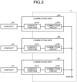
- FIG. 2 is a diagram illustrating an exemplary schematic configuration of the connection units. Three connection units of a connection unit 6a, a connection unit 6b, and a connection unit 6c are illustrated.
- connection unit 6a is a first connection unit that is provided between the contact 4a and the ground GND.
- the connection unit 6a includes a contact portion 61a and a connection circuit 62a.
- the contact portion 61a brings the contact 4a into contact with the substrate 1.
- the configuration of the contact portion 61a is not particularly limited, but for example, a contact terminal such as a contact spring, a conductive screw, or the like may be used.
- connection circuit 62a is connected between the contact portion 61a and the ground GND.
- the connection circuit 62a defines a connection state between the contact portion 61a and the ground GND, that is, a connection state between the contact 4a of the parasitic antenna element 4 and the ground GND.
- Various definition of the connection state enables the parasitic antenna element 4 to have more resonance frequencies.
- connection state examples include a state (short-circuit state) in which the contact 4a is connected to the ground GND and a state (e.g., open state) in which the contact 4a is not connected to the ground GND.
- the connection circuit 62a may define the connection state for each frequency band. For example, the connection circuit 62a brings the contact 4a into the short-circuit state in a specific frequency band and brings the contact 4a into the open state in another frequency band.
- the connection circuit 62a having such a configuration includes, for example, a filter.
- An example of a filter includes a bandpass filter that passes a signal in the specific frequency band.
- a filter circuit configured to include coils and/or capacitors provided in series and/or in parallel may be used.
- connection state examples include an impedance and a phase from the contact 4a to the ground GND. This impedance and phase adjust the electrical length of the first portion 41 of the parasitic antenna element 4, and further the resonance frequency of the first portion 41.
- the connection circuit 62a may define the connection state according to the frequency band used. For example, the connection circuit 62a adjusts the impedance and the phase from the contact 4a to the ground GND so that the resonance frequency of the first portion 41 of the parasitic antenna element 4 is included in the frequency band used.
- the connection circuit 62a having such a configuration includes an active element.
- An example of the active element is a switch such as SP4T. The switch is provided so as to provide a plurality of paths from the contact 4a to the ground GND.
- Circuit elements and the like may be provided on several paths so that the paths have different impedances and phases.
- the switch switches the impedances and the phases from the contact 4a to the ground GND.
- the antenna device 100 may also include a control unit and the like necessary for switch control.
- connection circuit 62a may have a configuration in which both configurations of the filter and the switch described above are combined.
- the connection unit 6b is a second connection unit that is provided between the contact 4b and the ground GND.
- the connection unit 6b includes a contact portion 61b and a connection circuit 62b.
- the contact portion 61b brings the contact 4b into contact with the substrate 1.
- the connection circuit 62b defines a connection state between the contact portion 61b and the ground GND, that is, a connection state between the contact 4b of the parasitic antenna element 4 and the ground GND. Details are similar to those of the contact portion 61a and connection circuit 62a described above, and thus the description thereof will not be repeated.
- a specific frequency band (e.g., passband of the filter) in which the connection circuit 62b changes the connection state into the short-circuit state may be a frequency band different from the specific frequency band in the connection circuit 62a described above.
- the connection unit 6c is a third connection unit that is provided between the contact 4c and the ground GND.
- the connection unit 6c includes a contact portion 61c and a connection circuit 62c.
- the contact portion 61c brings the contact 4c into contact with the substrate 1.
- the connection circuit 62c defines a connection state between the contact portion 61c and the ground GND, that is, a connection state between the contact 4c of the parasitic antenna element 4 and the ground GND. Details are similar to those of the contact portion 61a and connection circuit 62a described above, and thus the description thereof will not be repeated.
- a specific frequency band in which the connection circuit 62c changes the connection state into the short-circuit state may be a frequency band different from the specific frequency band in the connection circuit 62a described above and the specific frequency band in the connection circuit 62b.
- the additional parasitic antenna element 5 is a parasitic antenna element different from the parasitic antenna element 4, and is provided on the substrate 1 in this example.
- One end portion of the additional parasitic antenna element 5 (end portion on a side near the feed antenna element 3, in this example) is connected to the ground GND.
- the additional parasitic antenna element 5 is electrically coupled to the feed antenna element 3 via the substrate 1.
- Examples of the additional parasitic antenna element 5 include an LDS antenna, a metal pattern formed on the substrate 1, and the like.
- the metal pattern is provided at a portion of the substrate 1 having no pattern of the ground GND.
- the LDS antenna may be provided at a portion of the substrate 1 having the pattern of the ground GND, or may be provided at a portion of the substrate 1 having no pattern of the ground GND.
- the additional parasitic antenna element 5 has a resonance frequency different from the resonance frequency of the feed antenna element 3 and the resonance frequency of the parasitic antenna element 4. Similarly to the resonance frequencies of the feed antenna element 3 and the parasitic antenna element 4, the resonance frequency of the additional parasitic antenna element 5 is also a frequency in the frequency band used for the antenna device 100.
- the resonance frequency of the additional parasitic antenna element 5 may be a frequency included in a band different from the band including the resonance frequency of the feed antenna element 3 and the band including the resonance frequency of the parasitic antenna element 4.
- the resonance frequency of the additional parasitic antenna element 5 may be lower than the resonance frequency of the feed antenna element 3.
- a plurality of coexistent resonant modes can coexist. Examples of some resonant modes will be described with reference to FIG. 3 .
- FIG. 3 is a table illustrating an example of a plurality of resonant modes. Exemplified are six resonant modes of a resonant mode M1 to a resonant mode M6 are exemplified.
- the resonant mode M1 is a mode of resonance at a frequency (first resonance frequency) at which the electrical length of the whole parasitic antenna element 4 is ⁇ /2.
- An example of the first resonance frequency is a frequency in a 700 MHz band.
- the contact 4a is in the short-circuit state.
- the contact 4b is in the open state.
- the contact 4c is in the short-circuit state.
- the resonant mode M2 is a mode of resonance at a frequency (second resonance frequency) at which the electrical length of the first portion 41 of the parasitic antenna element 4 is ⁇ /2.
- An example of the resonance frequency is a frequency in a 1800 MHz band.
- the contact 4a is in the short-circuit state.
- the contact 4b is in the short-circuit state.
- the contact 4c is in any state. In order to avoid unexpected unnecessary resonance or the like, the short-circuit state may be adopted, as any state.
- the resonant mode M3 is a mode of resonance at a frequency (third resonance frequency) at which the electrical length of the first portion 41 of the parasitic antenna element 4 is ⁇ /4.
- An example of the third resonance frequency is a frequency in a 900 MHz band.
- the contact 4a is in the open state.
- the contact 4b is in the short-circuit state.
- the contact 4c is in any state.
- the resonant mode M4 is a mode of resonance at a frequency (fourth resonance frequency) at which the electrical length of the second portion 42 of the parasitic antenna element 4 is ⁇ /2.
- An example of the fourth resonance frequency is a frequency in a 1500 MHz band.
- the contact 4a is in any state.
- the contact 4b is in the short-circuit state.
- the contact 4c is in the short-circuit state.
- the resonant mode M5 is a mode of resonance at a frequency (fifth resonance frequency) at which the electrical length of the feed antenna element 3 is ⁇ /4.
- An example of the fifth resonance frequency is a frequency in a 3500 MHz band.
- the contact 4a is in the short-circuit state.
- the contact 4b is in the short-circuit state.
- the contact 4c is in any state.
- the resonant mode M6 is a mode of resonance at a frequency (sixth resonance frequency) at which the electrical length of the additional parasitic antenna element 5 is ⁇ /4.
- An example of the sixth resonance frequency is a frequency in a 2500 MHz band.
- the contact 4a is in any state.
- the contact 4b is in any state.
- the contact 4c is in any state.
- connection circuit 62a, the connection circuit 62b, and the connection circuit 62c define the connection state for each frequency band.
- the connection circuit 62a brings the contact 4a into the short-circuit state in the 700 MHz band, 1800 MHz band, and 3500 MHz band, and brings the contact 4a into the open state in the 900 MHz band.
- the connection circuit 62b brings the contact 4b into the short-circuit state in the 1800 MHz band, 900 MHz band, 1500 MHz band, and 3500 MHz band, and brings the contact 4b into the open state in the 700 MHz band.
- the connection circuit 62c brings the contact 4c into the short-circuit state in the 700 MHz band and 1500 MHz band.
- the plurality of resonant modes as described above makes it possible for the antenna device 100 to support multiple bands.
- using the housing 2 including the parasitic antenna element 4 makes it possible to reduce the size of the antenna device 100, as compared with providing the parasitic antenna element 4 separately from the housing 2.
- connection units may not include the connection circuits.
- the contact portion 61c may be directly connected to the ground GND.
- the connection state of the contact 4c can be defined for each frequency band described above with reference to FIG. 3 .
- the number and positions of the contacts provided in the parasitic antenna element 4 are not limited to the contact 4a, the contact 4b, and the contact 4c. Any number of contacts may be provided at any position.
- a plurality of the additional parasitic antenna elements 5 may be provided.
- the frequency band including the resonance frequency is not limited to the specific frequency band described above with the numerical values.
- the antenna device 100 may be used by being incorporated into various devices such as a radar device, in addition to the communication apparatus.
- the antenna device 100 having described above is specified, for example, as follows. As described with reference to FIGS. 1 and 3 and the like, the antenna device 100 includes the feed antenna element 3, and the housing 2 that includes the parasitic antenna element 4 extending to be electrically coupled to the feed antenna element 3 and that has a resonance frequency different from that of the feed antenna element 3.
- the resonance frequency of the feed antenna element 3 and the resonance frequency of the parasitic antenna element 4 included in the housing 2 coexist, and therefore, multiple bands can be supported. Furthermore, the size of the antenna device 100 can be reduced, as compared with providing a parasitic antenna element separately from the housing 2.
- the antenna device 100 may include the connection unit 6a, the connection unit 6b, and the connection unit 6c that are provided between the parasitic antenna element 4 and the ground GND. This configuration makes it possible to ensure the ground of the parasitic antenna element 4 so that the parasitic antenna element 4 can have a resonance frequency according to itself.
- connection unit 6a, the connection unit 6b, and the connection unit 6c may include the connection circuit 62a, the connection circuit 62b, and the connection circuit 62c each of which defines the connection state between the parasitic antenna element 4 and the ground GND.
- the connection circuit 62a, the connection circuit 62b, and the connection circuit 62c may each include the filter that defines the connection state for each frequency band, or may each include the switch that defines the connection state according to the frequency band used. This configuration makes it possible for the parasitic antenna element 4 to have more resonance frequencies.
- the feed antenna element 3 may include the base portion 31 that has the feed point 3a, and the extending portion 32 that extends from the end portion of the base portion 31 to both sides.
- the feed antenna element 3 may include the base portion 31 that has the feed point 3a, and the extending portion 32 that extends from the end portion of the base portion 31 to both sides.
- an antenna having such a T-shape can be used as the feed antenna element 3.
- the parasitic antenna element 4 may include the first portion 41 that extends along the extending direction of the feed antenna element 3 so as to generate capacitive coupling with the feed antenna element 3, and the second portion 42 that contiguously extends from the first portion 41.
- the parasitic antenna element 4 can be electrically coupled to the feed antenna element 3.
- the length of the first portion 41 of the parasitic antenna element 4 may be longer than the length of the feed antenna element 3. Therefore, electrical coupling between the first portion 41 of the parasitic antenna element 4 and the feed antenna element 3 can be enhanced.
- connection unit 6a may be the first connection unit that is provided between the ground GND and one end portion (portion where the contact 4a is provided) of the first portion 41 of the parasitic antenna element 4.
- the connection unit 6b may be the second connection unit that is provided between the ground GND and the other end portion (portion where the contact 4b is provided) of the first portion 41 of the parasitic antenna element 4.
- the connection unit 6c may be the third connection unit that is provided between the ground GND and the end portion (portion where the contact 4b is provided) of the second portion 42 of the parasitic antenna element 4, provided on the opposite side of the first portion 41.
- the parasitic antenna element 4 may have a resonance frequency that is lower than the resonance frequency of the feed antenna element 3. Therefore, for example, it is possible to couple the feed antenna element 3 to the parasitic antenna element 4, as the transmission path, without interfering with the radiation of the feed antenna element 3 alone.
- the antenna device 100 may include the additional parasitic antenna element 5 that is electrically coupled to the feed antenna element 3 and that has a resonance frequency different from the resonance frequency of the parasitic antenna element 4 and the resonance frequency of the additional parasitic antenna element 5.
- the additional parasitic antenna element 5 may be electrically coupled to the feed antenna element 3 via the substrate 1.
- the additional parasitic antenna element 5 may have a resonance frequency that is lower than the resonance frequency of the feed antenna element 3. Providing the additional parasitic antenna element 5 having such a configuration makes it possible to increase the number of coexisting resonance frequencies, and further multiple bands can be supported.
- the communication apparatus is also provided to perform communication by using the antenna device 100.
- the communication apparatus includes the feed antenna element 3, and the housing 2 that includes the parasitic antenna element 4 extending to be electrically coupled to the feed antenna element 3 and that has a resonance frequency different from that of the feed antenna element 3, and the communication apparatus performs communication by using the feed antenna element 3. Even in the communication apparatus having such a configuration, it is possible to support multiple bands and to reduce the size of the device.
- Power may be supplied to the parasitic antenna element 4.
- power may be fed to the parasitic antenna element 4 (second antenna element) may be performed, together with power feeding to the feed antenna element 3 (first antenna element) or instead of power feeding to the feed antenna element 3. Even in this configuration, it is possible to support multiple bands and reduce the size of the device.
Landscapes
- Engineering & Computer Science (AREA)
- Computer Networks & Wireless Communication (AREA)
- Support Of Aerials (AREA)
- Details Of Aerials (AREA)
- Variable-Direction Aerials And Aerial Arrays (AREA)
Abstract
Description
- The present disclosure relates to an antenna device and a communication apparatus.
- For example,
Patent Literature 1 discloses a method to make a housing have the same resonance frequency as that of a feed antenna element, in order to reduce an influence of the housing on a radiation characteristic of the feed antenna element. - Patent Literature 1:
WO 2016/125556 A - It is considered that the resonance frequency of the housing may be used for supporting multiple bands. However,
Patent Literature 1 has not studied this point at all. - One aspect of the present disclosure provides an antenna device and a communication apparatus that are configured to support multiple bands.
- An antenna device according to one aspect of the present disclosure includes: a feed antenna element; and a housing that includes a parasitic antenna element extending to be electrically coupled to the feed antenna element and having a resonance frequency different from that of the feed antenna element.
- A communication apparatus according to one aspect of the present disclosure includes: a feed antenna element; and a housing that includes a parasitic antenna element extending to be electrically coupled to the feed antenna element and having a resonance frequency different from that of the feed antenna element, wherein communication is performed by using the feed antenna element.
-
-
FIG. 1 is a diagram illustrating an exemplary schematic configuration of an antenna device according to an embodiment. -
FIG. 2 is a diagram illustrating an exemplary schematic configuration of connection units. -
FIG. 3 is a table illustrating an example of a plurality of resonance frequencies. - The embodiments of the present disclosure will be described in detail below with reference to the drawings. Note that in the following embodiments, the same elements are denoted by the same reference numerals and symbols, and redundant description thereof will be omitted.
- Furthermore, the present disclosure will be described in the order of items shown below.
-
FIG. 1 is a diagram illustrating an exemplary schematic configuration of an antenna device according to an embodiment.FIG. 1 is also a diagram illustrating a schematic configuration of part of a communication apparatus in which the antenna device is incorporated. An example of the communication apparatus includes a mobile communication apparatus such as a smartphone. The communication apparatus performs communication by using theantenna device 100, more specifically, afeed antenna element 3 and the like which will be described later. - The
antenna device 100 includes asubstrate 1, ahousing 2, thefeed antenna element 3, aparasitic antenna element 4, and an additionalparasitic antenna element 5. As will be described later, theparasitic antenna element 4 is included in thehousing 2. For convenience of description, an XYZ coordinate system is illustrated. An X-axis direction and a Y-axis direction correspond to a plane direction of thesubstrate 1. A Z-axis direction corresponds to a thickness direction of thesubstrate 1. - The
substrate 1 has a ground having a reference potential (hereinafter, referred to as "ground GND"). Thesubstrate 1 is provided with various other elements in addition to the illustrated elements. Examples of the other elements include a circuit that generates a transmission signal of thefeed antenna element 3, a circuit that performs processing or the like of a reception signal, and the like. - The
housing 2 houses thesubstrate 1, thefeed antenna element 3, and the additionalparasitic antenna element 5. The other elements which are not illustrated (e.g., a battery of the communication apparatus) can also be housed in thehousing 2. Thehousing 2 includes ahousing 21 and ahousing 22. Thehousing 21 and thehousing 22 constitute, on an XY plane, a frame body (frame portion) surrounding thesubstrate 1, thefeed antenna element 3, and the additionalparasitic antenna element 5. - The
housing 21 constitutes an upper portion (a portion in a positive Y-axis direction) of the frame body. Thehousing 21 constitutes an upper side portion and corner portions on both sides of the frame body. Thehousing 22 constitutes at least part of a portion below the housing 21 (portion in a negative Y-axis direction). - The
housing 21 and thehousing 22 have conductivity. An example of the material thereof is metal. Thehousing 21 and thehousing 22 are separated from each other in thehousing 2. In this example, a gap is provided between thehousing 21 and thehousing 22. The portion of the gap may be filled with an insulator such as resin. An upper end portion (a portion opposed to the housing 21) of thehousing 22 may be connected to the ground GND. - The
housing 21 also has a certain length in the Z-axis direction so as to have an inner side surface facing thefeed antenna element 3 and the like. - The
feed antenna element 3 has a resonance frequency. The resonance frequency of thefeed antenna element 3 is a frequency in a frequency band used for theantenna device 100. An example of the frequency band used is a communication frequency band for the communication apparatus. Examples of the communication frequency band include a band of 700 MHz to 960 MHz, a band of 1400 MHz to 1510 MHz, a band of 1710 MHz to 2200 MHz, a band of 2300 MHz to 2700 MHz, a band of 3400 MHz to 3600 MHz, a band of 3600 MHz to 4100 MHz, and a band of 4500 MHz to 4600 MHz. - Examples of the
feed antenna element 3 include a laser direct structuring (LDS) antenna, a metal pattern formed on thesubstrate 1, and the like. In this example, thefeed antenna element 3 is provided near a corner on the left side (in a negative X-axis direction) of thehousing 22. However, the position of thefeed antenna element 3 is not limited to that in the example illustrated inFIG. 1 . - The illustrated
feed antenna element 3 includes abase portion 31, an extendingportion 32, an extendingportion 33, and an extendingportion 34. Thebase portion 31 extends from one end portion having afeed point 3a toward the corner of thehousing 22, in an upper left direction (direction between the negative X-axis direction and the positive Y-axis direction). However, the shape of thefeed antenna element 3 is not limited to that in the example illustrated inFIG. 1 . Thefeed antenna element 3 may have various shapes such as an L-shape, in addition to the substantially T-shape as illustrated inFIG. 1 . - The extending
portion 32 extends from an end portion of thebase portion 31 to both sides. The extendingportion 33 is connected to one end portion of the extendingportion 32 and extends in a direction different from an extending direction of the extendingportion 32. The extendingportion 34 is connected to the other end portion of the extendingportion 32 and extends in a direction different from the extending direction of the extendingportion 32. The extendingportion 32, the extendingportion 33, and the extendingportion 34 almost extend along the corner portion of thehousing 21. In this example, the extendingportion 32 extends facing the corner of thehousing 21. The extendingportion 33 extends downward (negative Y-axis direction), along a left side portion (portion in the negative X-axis direction) of thehousing 21. The extendingportion 34 extends rightward (positive X-axis direction) along the upper side portion of thehousing 21. Note that at least some of the extendingportion 32, the extendingportion 33, and the extendingportion 34 may be smoothly curved, for example, along the corner of thehousing 21. - The extending
portion 32, the extendingportion 33, and the extendingportion 34 have a certain length in the Z-axis direction as well so as to have a surface facing the inner side surface of thehousing 21 which has been described above. Specifically, the extendingportion 32 has a surface facing the inner side surface of the corner portion of thehousing 21. The extendingportion 33 has a surface (surface extending in a YZ plane direction) facing the inner side surface of the left side portion of thehousing 21. The extendingportion 34 has a surface (surface extending in an XZ plane direction) facing the inner side surface of the upper side portion of thehousing 21. - The
feed antenna element 3 has a resonance frequency according to an electrical length of thefeed antenna element 3. The electrical length of thefeed antenna element 3 is mainly given by the extendingportion 32, the extendingportion 33, and the extendingportion 34. The resonance frequency of thefeed antenna element 3 is a frequency at which the electrical length from a feed point F to an end of the extendingportion 33 or an end of the extendingportion 34 is λ/4 (λ is a wavelength). - The
parasitic antenna element 4 is included in the housing 2 (is part of the housing 2). In this example, theparasitic antenna element 4 is thehousing 21. Theparasitic antenna element 4 extends so as to be electrically coupled to thefeed antenna element 3 in the frequency band used for theantenna device 100. The electrical connection between thefeed antenna element 3 and theparasitic antenna element 4 includes capacitive coupling. - The
parasitic antenna element 4 has a resonance frequency according to an electrical length of each portion (first portion 41 and asecond portion 42 which will be described later) of theparasitic antenna element 4. Similarly to the resonance frequency of thefeed antenna element 3, the resonance frequency of theparasitic antenna element 4 is also a frequency in the frequency band used for theantenna device 100. The resonance frequency of theparasitic antenna element 4 is different from the resonance frequency of thefeed antenna element 3. The resonance frequency of theparasitic antenna element 4 may be a frequency included in a band different from the band including the resonance frequency of thefeed antenna element 3. Theparasitic antenna element 4 may have a plurality of resonance frequencies included in different bands. - The resonance frequency of the
parasitic antenna element 4 may be lower than the resonance frequency of thefeed antenna element 3. When the resonance frequency of theparasitic antenna element 4 is lower than the resonance frequency of thefeed antenna element 3, thefeed antenna element 3 is reduced in size relative to theparasitic antenna element 4. Therefore, thefeed antenna element 3 can be structurally included in theparasitic antenna element 4, contributing to reduction in size. In addition, thefeed antenna element 3 is allowed to be coupled to theparasitic antenna element 4, as a transmission path, without interfering with radiation of thefeed antenna element 3 alone. - The
parasitic antenna element 4 includes thefirst portion 41 and thesecond portion 42. In this example, thefirst portion 41 is a portion positioned on the left side (in the negative X-axis direction), and thesecond portion 42 is a portion positioned on the right side (in the positive X-axis direction). Thefirst portion 41 has a length (boundary with the second portion 42) is determined by the position of acontact 4b which is described later. Thefirst portion 41 is a portion on the left side including thecontact 4b, and thesecond portion 42 is a portion on the right side from thecontact 4b. - The
first portion 41 corresponds to the corner portion on the left side of thehousing 21. Thefirst portion 41 extends along the extending direction of thefeed antenna element 3 so as to generate the capacitive coupling with the feed antenna element 3 (constitution of a transmission line). Thehousing 21 faces the extendingportion 32, the extendingportion 33, and the extendingportion 34 of thefeed antenna element 3, at the corner portion, which causes the capacitive coupling between thefirst portion 41 and thefeed antenna element 3. - The length of the
first portion 41 is preferably longer than the length of thefeed antenna element 3. Therefore, electrical coupling between thefirst portion 41 of theparasitic antenna element 4 and thefeed antenna element 3 can be enhanced. Specifically, the resonance frequency of theparasitic antenna element 4 lower than the resonance frequency of thefeed antenna element 3 makes it possible to couple thefeed antenna element 3, as the transmission path, to theparasitic antenna element 4 without interfering with the radiation of thefeed antenna element 3 alone. - The
second portion 42 contiguously extends from thefirst portion 41. Thesecond portion 42 is electrically coupled to thefeed antenna element 3 via thefirst portion 41. - The
parasitic antenna element 4 includes acontact 4a, thecontact 4b, and acontact 4c that are connectable to the ground GND. - The
contact 4a and thecontact 4b are provided in thefirst portion 41. Thecontact 4a is provided at one end portion of the first portion 41 (end portion on a side opposite to the second portion 42). Thecontact 4b is provided at the other end portion of the first portion 41 (end portion on a side to the second portion 42). In other words, thecontact 4b determines the position of the other end portion of the first portion 41 (boundary between thefirst portion 41 and the second portion 42) in theparasitic antenna element 4. - The
contact 4c is provided in thesecond portion 42. Thecontact 4c is provided at the other end portion of the second portion 42 (end portion on a side opposite to the first portion 41). Note that one end portion of the second portion 42 (end portion on a side to the first portion 41) is connected to the other end portion of thefirst portion 41. - The
antenna device 100 also includes connection units that are configured to connect thecontact 4a, thecontact 4b, and thecontact 4c to the ground GND. This configuration makes it possible to ensure the ground of theparasitic antenna element 4 so that theparasitic antenna element 4 can have the resonance frequency. The connection units will be described with reference toFIG. 2 . -
FIG. 2 is a diagram illustrating an exemplary schematic configuration of the connection units. Three connection units of aconnection unit 6a, aconnection unit 6b, and aconnection unit 6c are illustrated. - The
connection unit 6a is a first connection unit that is provided between thecontact 4a and the ground GND. Theconnection unit 6a includes a contact portion 61a and aconnection circuit 62a. - The contact portion 61a brings the
contact 4a into contact with thesubstrate 1. The configuration of the contact portion 61a is not particularly limited, but for example, a contact terminal such as a contact spring, a conductive screw, or the like may be used. - The
connection circuit 62a is connected between the contact portion 61a and the ground GND. Theconnection circuit 62a defines a connection state between the contact portion 61a and the ground GND, that is, a connection state between thecontact 4a of theparasitic antenna element 4 and the ground GND. Various definition of the connection state enables theparasitic antenna element 4 to have more resonance frequencies. - Examples of the connection state include a state (short-circuit state) in which the
contact 4a is connected to the ground GND and a state (e.g., open state) in which thecontact 4a is not connected to the ground GND. Theconnection circuit 62a may define the connection state for each frequency band. For example, theconnection circuit 62a brings thecontact 4a into the short-circuit state in a specific frequency band and brings thecontact 4a into the open state in another frequency band. Theconnection circuit 62a having such a configuration includes, for example, a filter. An example of a filter includes a bandpass filter that passes a signal in the specific frequency band. For the filter, a filter circuit configured to include coils and/or capacitors provided in series and/or in parallel may be used. - Other examples of the connection state include an impedance and a phase from the
contact 4a to the ground GND. This impedance and phase adjust the electrical length of thefirst portion 41 of theparasitic antenna element 4, and further the resonance frequency of thefirst portion 41. Theconnection circuit 62a may define the connection state according to the frequency band used. For example, theconnection circuit 62a adjusts the impedance and the phase from thecontact 4a to the ground GND so that the resonance frequency of thefirst portion 41 of theparasitic antenna element 4 is included in the frequency band used. Theconnection circuit 62a having such a configuration includes an active element. An example of the active element is a switch such as SP4T. The switch is provided so as to provide a plurality of paths from thecontact 4a to the ground GND. Circuit elements and the like may be provided on several paths so that the paths have different impedances and phases. The switch switches the impedances and the phases from thecontact 4a to the ground GND. Theantenna device 100 may also include a control unit and the like necessary for switch control. - The
connection circuit 62a may have a configuration in which both configurations of the filter and the switch described above are combined. - The
connection unit 6b is a second connection unit that is provided between thecontact 4b and the ground GND. Theconnection unit 6b includes a contact portion 61b and aconnection circuit 62b. The contact portion 61b brings thecontact 4b into contact with thesubstrate 1. Theconnection circuit 62b defines a connection state between the contact portion 61b and the ground GND, that is, a connection state between thecontact 4b of theparasitic antenna element 4 and the ground GND. Details are similar to those of the contact portion 61a andconnection circuit 62a described above, and thus the description thereof will not be repeated. A specific frequency band (e.g., passband of the filter) in which theconnection circuit 62b changes the connection state into the short-circuit state may be a frequency band different from the specific frequency band in theconnection circuit 62a described above. - The
connection unit 6c is a third connection unit that is provided between thecontact 4c and the ground GND. Theconnection unit 6c includes a contact portion 61c and aconnection circuit 62c. The contact portion 61c brings thecontact 4c into contact with thesubstrate 1. Theconnection circuit 62c defines a connection state between the contact portion 61c and the ground GND, that is, a connection state between thecontact 4c of theparasitic antenna element 4 and the ground GND. Details are similar to those of the contact portion 61a andconnection circuit 62a described above, and thus the description thereof will not be repeated. A specific frequency band in which theconnection circuit 62c changes the connection state into the short-circuit state may be a frequency band different from the specific frequency band in theconnection circuit 62a described above and the specific frequency band in theconnection circuit 62b. - Returning to
FIG. 1 , the additionalparasitic antenna element 5 will be described. The additionalparasitic antenna element 5 is a parasitic antenna element different from theparasitic antenna element 4, and is provided on thesubstrate 1 in this example. One end portion of the additional parasitic antenna element 5 (end portion on a side near thefeed antenna element 3, in this example) is connected to the ground GND. The additionalparasitic antenna element 5 is electrically coupled to thefeed antenna element 3 via thesubstrate 1. Examples of the additionalparasitic antenna element 5 include an LDS antenna, a metal pattern formed on thesubstrate 1, and the like. The metal pattern is provided at a portion of thesubstrate 1 having no pattern of the ground GND. The LDS antenna may be provided at a portion of thesubstrate 1 having the pattern of the ground GND, or may be provided at a portion of thesubstrate 1 having no pattern of the ground GND. - The additional
parasitic antenna element 5 has a resonance frequency different from the resonance frequency of thefeed antenna element 3 and the resonance frequency of theparasitic antenna element 4. Similarly to the resonance frequencies of thefeed antenna element 3 and theparasitic antenna element 4, the resonance frequency of the additionalparasitic antenna element 5 is also a frequency in the frequency band used for theantenna device 100. The resonance frequency of the additionalparasitic antenna element 5 may be a frequency included in a band different from the band including the resonance frequency of thefeed antenna element 3 and the band including the resonance frequency of theparasitic antenna element 4. The resonance frequency of the additionalparasitic antenna element 5 may be lower than the resonance frequency of thefeed antenna element 3. - In the
antenna device 100 having the configuration described above, a plurality of coexistent resonant modes can coexist. Examples of some resonant modes will be described with reference toFIG. 3 . -
FIG. 3 is a table illustrating an example of a plurality of resonant modes. Exemplified are six resonant modes of a resonant mode M1 to a resonant mode M6 are exemplified. - The resonant mode M1 is a mode of resonance at a frequency (first resonance frequency) at which the electrical length of the whole
parasitic antenna element 4 is λ/2. An example of the first resonance frequency is a frequency in a 700 MHz band. At the first resonance frequency, thecontact 4a is in the short-circuit state. Thecontact 4b is in the open state. Thecontact 4c is in the short-circuit state. - The resonant mode M2 is a mode of resonance at a frequency (second resonance frequency) at which the electrical length of the
first portion 41 of theparasitic antenna element 4 is λ/2. An example of the resonance frequency is a frequency in a 1800 MHz band. At the second resonance frequency, thecontact 4a is in the short-circuit state. Thecontact 4b is in the short-circuit state. Thecontact 4c is in any state. In order to avoid unexpected unnecessary resonance or the like, the short-circuit state may be adopted, as any state. - The resonant mode M3 is a mode of resonance at a frequency (third resonance frequency) at which the electrical length of the
first portion 41 of theparasitic antenna element 4 is λ/4. An example of the third resonance frequency is a frequency in a 900 MHz band. At the third resonance frequency, thecontact 4a is in the open state. Thecontact 4b is in the short-circuit state. Thecontact 4c is in any state. - The resonant mode M4 is a mode of resonance at a frequency (fourth resonance frequency) at which the electrical length of the
second portion 42 of theparasitic antenna element 4 is λ/2. An example of the fourth resonance frequency is a frequency in a 1500 MHz band. At the fourth resonance frequency, thecontact 4a is in any state. Thecontact 4b is in the short-circuit state. Thecontact 4c is in the short-circuit state. - The resonant mode M5 is a mode of resonance at a frequency (fifth resonance frequency) at which the electrical length of the
feed antenna element 3 is λ/4. An example of the fifth resonance frequency is a frequency in a 3500 MHz band. At the fifth resonance frequency, thecontact 4a is in the short-circuit state. Thecontact 4b is in the short-circuit state. Thecontact 4c is in any state. - The resonant mode M6 is a mode of resonance at a frequency (sixth resonance frequency) at which the electrical length of the additional
parasitic antenna element 5 is λ/4. An example of the sixth resonance frequency is a frequency in a 2500 MHz band. At the sixth resonance frequency, thecontact 4a is in any state. Thecontact 4b is in any state. Thecontact 4c is in any state. - As described above, the
connection circuit 62a, theconnection circuit 62b, and theconnection circuit 62c define the connection state for each frequency band. In the example illustrated inFIG. 3 , theconnection circuit 62a brings thecontact 4a into the short-circuit state in the 700 MHz band, 1800 MHz band, and 3500 MHz band, and brings thecontact 4a into the open state in the 900 MHz band. Theconnection circuit 62b brings thecontact 4b into the short-circuit state in the 1800 MHz band, 900 MHz band, 1500 MHz band, and 3500 MHz band, and brings thecontact 4b into the open state in the 700 MHz band. Theconnection circuit 62c brings thecontact 4c into the short-circuit state in the 700 MHz band and 1500 MHz band. When theconnection circuit 62a or the like adjusts the impedance and the phase between thecontact 4a or the like and the ground GND, for example, the first resonance frequency to the fourth resonance frequency can be also adjusted. - For example, the plurality of resonant modes as described above makes it possible for the
antenna device 100 to support multiple bands. In addition, using thehousing 2 including theparasitic antenna element 4 makes it possible to reduce the size of theantenna device 100, as compared with providing theparasitic antenna element 4 separately from thehousing 2. - The embodiments of the present disclosure have been described above, but the technical scope of the present disclosure is not limited to the embodiments described above, and various modifications and alterations can be made without departing from the spirit and scope of the present disclosure. Some examples will be described.
- Some of the connection units may not include the connection circuits. For example, in a case where the
connection unit 6c does not include theconnection circuit 62c, the contact portion 61c may be directly connected to the ground GND. Even in this case, the connection state of thecontact 4c can be defined for each frequency band described above with reference toFIG. 3 . - The number and positions of the contacts provided in the
parasitic antenna element 4 are not limited to thecontact 4a, thecontact 4b, and thecontact 4c. Any number of contacts may be provided at any position. - A plurality of the additional
parasitic antenna elements 5 may be provided. - The frequency band including the resonance frequency is not limited to the specific frequency band described above with the numerical values.
- The
antenna device 100 may be used by being incorporated into various devices such as a radar device, in addition to the communication apparatus. - The
antenna device 100 having described above is specified, for example, as follows. As described with reference toFIGS. 1 and3 and the like, theantenna device 100 includes thefeed antenna element 3, and thehousing 2 that includes theparasitic antenna element 4 extending to be electrically coupled to thefeed antenna element 3 and that has a resonance frequency different from that of thefeed antenna element 3. - According to the
antenna device 100 described above, the resonance frequency of thefeed antenna element 3 and the resonance frequency of theparasitic antenna element 4 included in thehousing 2 coexist, and therefore, multiple bands can be supported. Furthermore, the size of theantenna device 100 can be reduced, as compared with providing a parasitic antenna element separately from thehousing 2. - As described with reference to
FIG. 2 and the like, theantenna device 100 may include theconnection unit 6a, theconnection unit 6b, and theconnection unit 6c that are provided between theparasitic antenna element 4 and the ground GND. This configuration makes it possible to ensure the ground of theparasitic antenna element 4 so that theparasitic antenna element 4 can have a resonance frequency according to itself. - As described with reference to
FIGS. 2 and3 and the like, theconnection unit 6a, theconnection unit 6b, and theconnection unit 6c may include theconnection circuit 62a, theconnection circuit 62b, and theconnection circuit 62c each of which defines the connection state between theparasitic antenna element 4 and the ground GND. Theconnection circuit 62a, theconnection circuit 62b, and theconnection circuit 62c may each include the filter that defines the connection state for each frequency band, or may each include the switch that defines the connection state according to the frequency band used. This configuration makes it possible for theparasitic antenna element 4 to have more resonance frequencies. - As described with reference to
FIG. 1 and the like, thefeed antenna element 3 may include thebase portion 31 that has thefeed point 3a, and the extendingportion 32 that extends from the end portion of thebase portion 31 to both sides. For example, an antenna having such a T-shape can be used as thefeed antenna element 3. - As described with reference to
FIG. 1 and the like, theparasitic antenna element 4 may include thefirst portion 41 that extends along the extending direction of thefeed antenna element 3 so as to generate capacitive coupling with thefeed antenna element 3, and thesecond portion 42 that contiguously extends from thefirst portion 41. For example, in this way, theparasitic antenna element 4 can be electrically coupled to thefeed antenna element 3. - As described with reference to
FIG. 1 and the like, the length of thefirst portion 41 of theparasitic antenna element 4 may be longer than the length of thefeed antenna element 3. Therefore, electrical coupling between thefirst portion 41 of theparasitic antenna element 4 and thefeed antenna element 3 can be enhanced. - As described with reference to
FIGS. 1 and2 and the like, theconnection unit 6a may be the first connection unit that is provided between the ground GND and one end portion (portion where thecontact 4a is provided) of thefirst portion 41 of theparasitic antenna element 4. Theconnection unit 6b may be the second connection unit that is provided between the ground GND and the other end portion (portion where thecontact 4b is provided) of thefirst portion 41 of theparasitic antenna element 4. Theconnection unit 6c may be the third connection unit that is provided between the ground GND and the end portion (portion where thecontact 4b is provided) of thesecond portion 42 of theparasitic antenna element 4, provided on the opposite side of thefirst portion 41. For example, providing a plurality of theconnection units parasitic antenna element 4 to have many resonance frequencies. - The
parasitic antenna element 4 may have a resonance frequency that is lower than the resonance frequency of thefeed antenna element 3. Therefore, for example, it is possible to couple thefeed antenna element 3 to theparasitic antenna element 4, as the transmission path, without interfering with the radiation of thefeed antenna element 3 alone. - As described with reference to
FIGS. 1 and3 and the like, theantenna device 100 may include the additionalparasitic antenna element 5 that is electrically coupled to thefeed antenna element 3 and that has a resonance frequency different from the resonance frequency of theparasitic antenna element 4 and the resonance frequency of the additionalparasitic antenna element 5. The additionalparasitic antenna element 5 may be electrically coupled to thefeed antenna element 3 via thesubstrate 1. The additionalparasitic antenna element 5 may have a resonance frequency that is lower than the resonance frequency of thefeed antenna element 3. Providing the additionalparasitic antenna element 5 having such a configuration makes it possible to increase the number of coexisting resonance frequencies, and further multiple bands can be supported. - According to an aspect of the present disclosure, the communication apparatus is also provided to perform communication by using the
antenna device 100. In other words, the communication apparatus includes thefeed antenna element 3, and thehousing 2 that includes theparasitic antenna element 4 extending to be electrically coupled to thefeed antenna element 3 and that has a resonance frequency different from that of thefeed antenna element 3, and the communication apparatus performs communication by using thefeed antenna element 3. Even in the communication apparatus having such a configuration, it is possible to support multiple bands and to reduce the size of the device. - Note that the effects described in the present disclosure are merely examples and the effects are not limited to those disclosed. Other effects may be provided. Power may be supplied to the
parasitic antenna element 4. For example, power may be fed to the parasitic antenna element 4 (second antenna element) may be performed, together with power feeding to the feed antenna element 3 (first antenna element) or instead of power feeding to thefeed antenna element 3. Even in this configuration, it is possible to support multiple bands and reduce the size of the device. - Note that the present technology can also employ the following configurations.
- (1) An antenna device comprising:
- a feed antenna element; and
- a housing that includes a parasitic antenna element extending to be electrically coupled to the feed antenna element and having a resonance frequency different from that of the feed antenna element.
- (2) The antenna device according to (1), further comprising
a connection unit that is provided between the parasitic antenna element and a ground. - (3) The antenna device according to (2), wherein
the connection unit includes a connection circuit that defines a connection state between the parasitic antenna element and the ground. - (4) The antenna device according to (3), wherein
the connection circuit includes a filter that defines the connection state for each frequency band. - (5) The antenna device according to (3) or (4), wherein
the connection circuit includes a switch that defines the connection state according to a frequency band used. - (6) The antenna device according to any one of (1) to (5), wherein
- the feed antenna element includes:
- a base portion that has a feed point; and
- an extending portion that extends from an end portion of the base portion to both sides.
- (7) The antenna device according to any one of (1) to (6), wherein
the parasitic antenna element includes:- a first portion that extends along an extending direction of the feed antenna element so as to generate capacitive coupling with the feed antenna element; and
- a second portion that contiguously extends from the first portion.
- (8) The antenna device according to (7), wherein
a length of the first portion of the parasitic antenna element is longer than a length of the feed antenna element. - (9) The antenna device according to (7) or (8), further comprising
- a plurality of connection units that are connected between the parasitic antenna element and a ground,
- wherein the plurality of connection units includes:
- a first connection unit that is provided between one end portion of the first portion of the parasitic antenna element and the ground; and
- a second connection unit that is provided between the other end portion of the first portion of the parasitic antenna element and the ground.
- (10) The antenna device according to (9), wherein
the plurality of connection units includes a third connection unit that is provided between the ground and an end portion of the second portion of the parasitic antenna element provided on a side opposite to the first portion. - (11) The antenna device according to any one of (1) to (10), wherein
the resonance frequency of the parasitic antenna element is lower than the resonance frequency of the feed antenna element. - (12) The antenna device according to any one of (1) to (11), further comprising
an additional parasitic antenna element that is electrically coupled to the feed antenna element and that has a resonance frequency different from the resonance frequency of the feed antenna element and the resonance frequency of the parasitic antenna element. - (13) The antenna device according to (12), wherein
the additional parasitic antenna element is electrically coupled to the feed antenna element via a substrate. - (14) The antenna device according to (12) or (13), wherein
the resonance frequency of the additional parasitic antenna element is lower than the resonance frequency of the feed antenna element. - (15) A communication apparatus comprising:
- a feed antenna element; and
- a housing that includes a parasitic antenna element extending to be electrically coupled to the feed antenna element and having a resonance frequency different from that of the feed antenna element,
- wherein communication is performed by using the feed antenna element.
-
- 1
- SUBSTRATE
- 2
- HOUSING
- 21
- HOUSING
- 22
- HOUSING
- 3
- FEED ANTENNA ELEMENT
- 31
- BASE PORTION
- 32
- EXTENDING PORTION
- 33
- EXTENDING PORTION
- 34
- EXTENDING PORTION
- 4
- PARASITIC ANTENNA ELEMENT
- 41
- FIRST PORTION
- 42
- SECOND PORTION
- 4a
- CONTACT
- 4b
- CONTACT
- 4c
- CONTACT
- 5
- ADDITIONAL PARASITIC ANTENNA ELEMENT
- 6a
- CONNECTION UNIT
- 6b
- CONNECTION UNIT
- 6c
- CONNECTION UNIT
- 61a
- CONTACT PORTION
- 61b
- CONTACT PORTION
- 61c
- CONTACT PORTION
- 62a
- CONNECTION CIRCUIT
- 62b
- CONNECTION CIRCUIT
- 62c
- CONNECTION CIRCUIT
- 100
- ANTENNA DEVICE (COMMUNICATION APPARATUS)
Claims (15)
- An antenna device comprising:a feed antenna element; anda housing that includes a parasitic antenna element extending to be electrically coupled to the feed antenna element and having a resonance frequency different from that of the feed antenna element.
- The antenna device according to claim 1, further comprising
a connection unit that is provided between the parasitic antenna element and a ground. - The antenna device according to claim 2, wherein
the connection unit includes a connection circuit that defines a connection state between the parasitic antenna element and the ground. - The antenna device according to claim 3, wherein
the connection circuit includes a filter that defines the connection state for each frequency band. - The antenna device according to claim 3, wherein
the connection circuit includes a switch that defines the connection state according to a frequency band used. - The antenna device according to claim 1, wherein
the feed antenna element includes:a base portion that has a feed point; andan extending portion that extends from an end portion of the base portion to both sides. - The antenna device according to claim 1, wherein
the parasitic antenna element includes:a first portion that extends along an extending direction of the feed antenna element so as to generate capacitive coupling with the feed antenna element; anda second portion that contiguously extends from the first portion. - The antenna device according to claim 7, wherein
a length of the first portion of the parasitic antenna element is longer than a length of the feed antenna element. - The antenna device according to claim 7, further comprisinga plurality of connection units that are connected between the parasitic antenna element and a ground,wherein the plurality of connection units includes:a first connection unit that is provided between one end portion of the first portion of the parasitic antenna element and the ground; anda second connection unit that is provided between the other end portion of the first portion of the parasitic antenna element and the ground.
- The antenna device according to claim 9, wherein
the plurality of connection units includes a third connection unit that is provided between the ground and an end portion of the second portion of the parasitic antenna element provided on a side opposite to the first portion. - The antenna device according to claim 1, wherein
the resonance frequency of the parasitic antenna element is lower than the resonance frequency of the feed antenna element. - The antenna device according to claim 1, further comprising
an additional parasitic antenna element that is electrically coupled to the feed antenna element and that has a resonance frequency different from the resonance frequency of the feed antenna element and the resonance frequency of the parasitic antenna element. - The antenna device according to claim 12, wherein
the additional parasitic antenna element is electrically coupled to the feed antenna element via a substrate. - The antenna device according to claim 12, wherein
the resonance frequency of the additional parasitic antenna element is lower than the resonance frequency of the feed antenna element. - A communication apparatus comprising:a feed antenna element; anda housing that includes a parasitic antenna element extending to be electrically coupled to the feed antenna element and having a resonance frequency different from that of the feed antenna element,wherein communication is performed by using the feed antenna element.
Applications Claiming Priority (1)
| Application Number | Priority Date | Filing Date | Title |
|---|---|---|---|
| PCT/JP2020/037614 WO2022070419A1 (en) | 2020-10-02 | 2020-10-02 | Antenna device, and communication device |
Publications (2)
| Publication Number | Publication Date |
|---|---|
| EP4203190A1 true EP4203190A1 (en) | 2023-06-28 |
| EP4203190A4 EP4203190A4 (en) | 2023-10-18 |
Family
ID=80950111
Family Applications (1)
| Application Number | Title | Priority Date | Filing Date |
|---|---|---|---|
| EP20956347.7A Pending EP4203190A4 (en) | 2020-10-02 | 2020-10-02 | ANTENNA DEVICE AND COMMUNICATION DEVICE |
Country Status (3)
| Country | Link |
|---|---|
| EP (1) | EP4203190A4 (en) |
| JP (1) | JP7616231B2 (en) |
| WO (1) | WO2022070419A1 (en) |
Family Cites Families (9)
| Publication number | Priority date | Publication date | Assignee | Title |
|---|---|---|---|---|
| JPWO2004047223A1 (en) * | 2002-11-18 | 2006-03-23 | 株式会社ヨコオ | Multi-band antenna |
| EP2048739A4 (en) * | 2006-07-28 | 2009-08-05 | Murata Manufacturing Co | Antenna device and radio communication device |
| JP5603020B2 (en) * | 2009-03-26 | 2014-10-08 | 日本電気株式会社 | Antenna device |
| JP5435338B2 (en) * | 2009-06-15 | 2014-03-05 | 日立金属株式会社 | Multiband antenna |
| US20150222020A1 (en) * | 2012-09-24 | 2015-08-06 | Qualcomm Incorporated | Tunable antenna structure |
| KR20160024428A (en) * | 2014-08-25 | 2016-03-07 | 삼성전자주식회사 | Antenna Including Coupling Structure and Electronic Device |
| JP6320578B2 (en) | 2015-02-03 | 2018-05-09 | シャープ株式会社 | transceiver |
| CN106785421A (en) * | 2017-03-16 | 2017-05-31 | 宇龙计算机通信科技(深圳)有限公司 | Antenna system and the communication terminal with the antenna system |
| CN109462016A (en) * | 2018-09-29 | 2019-03-12 | Oppo广东移动通信有限公司 | Antenna device and electronic apparatus |
-
2020
- 2020-10-02 EP EP20956347.7A patent/EP4203190A4/en active Pending
- 2020-10-02 JP JP2022553408A patent/JP7616231B2/en active Active
- 2020-10-02 WO PCT/JP2020/037614 patent/WO2022070419A1/en not_active Ceased
Also Published As
| Publication number | Publication date |
|---|---|
| WO2022070419A1 (en) | 2022-04-07 |
| JPWO2022070419A1 (en) | 2022-04-07 |
| EP4203190A4 (en) | 2023-10-18 |
| JP7616231B2 (en) | 2025-01-17 |
Similar Documents
| Publication | Publication Date | Title |
|---|---|---|
| AU2015101172A4 (en) | Electronic device antenna with interference mitigation circuitry | |
| US6348894B1 (en) | Radio frequency antenna | |
| AU2016100564A4 (en) | Electronic device with tunable hybrid antennas | |
| US6573867B1 (en) | Small embedded multi frequency antenna for portable wireless communications | |
| KR20200024301A (en) | Electronic device slot antennas | |
| WO2011067944A1 (en) | Portable radio | |
| CN106129613B (en) | Antenna structure capable of adjusting radiation field type | |
| JP6504207B2 (en) | Antenna device and electronic device | |
| CN105337036A (en) | Mobile terminal and antenna structure thereof | |
| US11240909B2 (en) | Antenna device | |
| CN1816941B (en) | small diversity antenna | |
| TWI613866B (en) | Antenna structure with tunable radiation pattern | |
| US11303031B2 (en) | Antenna device and one set of antenna devices | |
| EP4203190A1 (en) | Antenna device, and communication device | |
| US20090224986A1 (en) | Radio apparatus and antenna device having element formed on casing material | |
| US11462815B2 (en) | Electronic device and antenna module | |
| CN107787535B (en) | Multi-magnetic loop antenna with single feed to parallel loops | |
| JP2018019225A (en) | Electronics | |
| US20250123697A1 (en) | Stylus Antenna | |
| JP7182137B2 (en) | Antenna device and communication device | |
| US12476372B2 (en) | Antenna device and communication device | |
| CN119009485B (en) | Antenna modules and electronic devices | |
| CN118867673A (en) | Electronic devices | |
| EP3226349B1 (en) | Antenna and terminal | |
| JP2023181038A (en) | Antenna equipment and communication equipment |
Legal Events
| Date | Code | Title | Description |
|---|---|---|---|
| STAA | Information on the status of an ep patent application or granted ep patent |
Free format text: STATUS: THE INTERNATIONAL PUBLICATION HAS BEEN MADE |
|
| PUAI | Public reference made under article 153(3) epc to a published international application that has entered the european phase |
Free format text: ORIGINAL CODE: 0009012 |
|
| STAA | Information on the status of an ep patent application or granted ep patent |
Free format text: STATUS: REQUEST FOR EXAMINATION WAS MADE |
|
| 17P | Request for examination filed |
Effective date: 20230322 |
|
| AK | Designated contracting states |
Kind code of ref document: A1 Designated state(s): AL AT BE BG CH CY CZ DE DK EE ES FI FR GB GR HR HU IE IS IT LI LT LU LV MC MK MT NL NO PL PT RO RS SE SI SK SM TR |
|
| REG | Reference to a national code |
Ref country code: DE Ref legal event code: R079 Free format text: PREVIOUS MAIN CLASS: H01Q0005378000 Ipc: H01Q0005385000 |
|
| A4 | Supplementary search report drawn up and despatched |
Effective date: 20230919 |
|
| RIC1 | Information provided on ipc code assigned before grant |
Ipc: H01Q 9/42 20060101ALI20230913BHEP Ipc: H01Q 5/392 20150101ALI20230913BHEP Ipc: H01Q 5/328 20150101ALI20230913BHEP Ipc: H01Q 1/24 20060101ALI20230913BHEP Ipc: H01Q 5/385 20150101AFI20230913BHEP |
|
| DAV | Request for validation of the european patent (deleted) | ||
| DAX | Request for extension of the european patent (deleted) |