EP4203006A2 - Electronic component with lid to manage radiation feedback - Google Patents
Electronic component with lid to manage radiation feedback Download PDFInfo
- Publication number
- EP4203006A2 EP4203006A2 EP22211991.9A EP22211991A EP4203006A2 EP 4203006 A2 EP4203006 A2 EP 4203006A2 EP 22211991 A EP22211991 A EP 22211991A EP 4203006 A2 EP4203006 A2 EP 4203006A2
- Authority
- EP
- European Patent Office
- Prior art keywords
- lid
- conductive layer
- internal
- electronic package
- semiconductor
- Prior art date
- Legal status (The legal status is an assumption and is not a legal conclusion. Google has not performed a legal analysis and makes no representation as to the accuracy of the status listed.)
- Pending
Links
Images





Classifications
-
- H—ELECTRICITY
- H10—SEMICONDUCTOR DEVICES; ELECTRIC SOLID-STATE DEVICES NOT OTHERWISE PROVIDED FOR
- H10W—GENERIC PACKAGES, INTERCONNECTIONS, CONNECTORS OR OTHER CONSTRUCTIONAL DETAILS OF DEVICES COVERED BY CLASS H10
- H10W76/00—Containers; Fillings or auxiliary members therefor; Seals
- H10W76/10—Containers or parts thereof
-
- H—ELECTRICITY
- H10—SEMICONDUCTOR DEVICES; ELECTRIC SOLID-STATE DEVICES NOT OTHERWISE PROVIDED FOR
- H10W—GENERIC PACKAGES, INTERCONNECTIONS, CONNECTORS OR OTHER CONSTRUCTIONAL DETAILS OF DEVICES COVERED BY CLASS H10
- H10W76/00—Containers; Fillings or auxiliary members therefor; Seals
- H10W76/10—Containers or parts thereof
- H10W76/17—Containers or parts thereof characterised by their materials
- H10W76/18—Insulating materials, e.g. resins, glasses or ceramics
-
- H—ELECTRICITY
- H10—SEMICONDUCTOR DEVICES; ELECTRIC SOLID-STATE DEVICES NOT OTHERWISE PROVIDED FOR
- H10W—GENERIC PACKAGES, INTERCONNECTIONS, CONNECTORS OR OTHER CONSTRUCTIONAL DETAILS OF DEVICES COVERED BY CLASS H10
- H10W42/00—Arrangements for protection of devices
- H10W42/20—Arrangements for protection of devices protecting against electromagnetic or particle radiation, e.g. light, X-rays, gamma-rays or electrons
-
- H—ELECTRICITY
- H10—SEMICONDUCTOR DEVICES; ELECTRIC SOLID-STATE DEVICES NOT OTHERWISE PROVIDED FOR
- H10W—GENERIC PACKAGES, INTERCONNECTIONS, CONNECTORS OR OTHER CONSTRUCTIONAL DETAILS OF DEVICES COVERED BY CLASS H10
- H10W42/00—Arrangements for protection of devices
- H10W42/20—Arrangements for protection of devices protecting against electromagnetic or particle radiation, e.g. light, X-rays, gamma-rays or electrons
- H10W42/261—Arrangements for protection of devices protecting against electromagnetic or particle radiation, e.g. light, X-rays, gamma-rays or electrons characterised by their shapes or dispositions
- H10W42/267—Patterned shielding planes
-
- H—ELECTRICITY
- H10—SEMICONDUCTOR DEVICES; ELECTRIC SOLID-STATE DEVICES NOT OTHERWISE PROVIDED FOR
- H10W—GENERIC PACKAGES, INTERCONNECTIONS, CONNECTORS OR OTHER CONSTRUCTIONAL DETAILS OF DEVICES COVERED BY CLASS H10
- H10W42/00—Arrangements for protection of devices
- H10W42/20—Arrangements for protection of devices protecting against electromagnetic or particle radiation, e.g. light, X-rays, gamma-rays or electrons
- H10W42/261—Arrangements for protection of devices protecting against electromagnetic or particle radiation, e.g. light, X-rays, gamma-rays or electrons characterised by their shapes or dispositions
- H10W42/273—Arrangements for protection of devices protecting against electromagnetic or particle radiation, e.g. light, X-rays, gamma-rays or electrons characterised by their shapes or dispositions the arrangements being between laterally adjacent chips, e.g. walls between chips
-
- H—ELECTRICITY
- H10—SEMICONDUCTOR DEVICES; ELECTRIC SOLID-STATE DEVICES NOT OTHERWISE PROVIDED FOR
- H10W—GENERIC PACKAGES, INTERCONNECTIONS, CONNECTORS OR OTHER CONSTRUCTIONAL DETAILS OF DEVICES COVERED BY CLASS H10
- H10W44/00—Electrical arrangements for controlling or matching impedance
- H10W44/20—Electrical arrangements for controlling or matching impedance at high-frequency [HF] or radio frequency [RF]
-
- H—ELECTRICITY
- H10—SEMICONDUCTOR DEVICES; ELECTRIC SOLID-STATE DEVICES NOT OTHERWISE PROVIDED FOR
- H10W—GENERIC PACKAGES, INTERCONNECTIONS, CONNECTORS OR OTHER CONSTRUCTIONAL DETAILS OF DEVICES COVERED BY CLASS H10
- H10W76/00—Containers; Fillings or auxiliary members therefor; Seals
- H10W76/10—Containers or parts thereof
- H10W76/12—Containers or parts thereof characterised by their shape
- H10W76/13—Containers comprising a conductive base serving as an interconnection
- H10W76/134—Containers comprising a conductive base serving as an interconnection having other interconnections parallel to the conductive base
-
- H—ELECTRICITY
- H10—SEMICONDUCTOR DEVICES; ELECTRIC SOLID-STATE DEVICES NOT OTHERWISE PROVIDED FOR
- H10W—GENERIC PACKAGES, INTERCONNECTIONS, CONNECTORS OR OTHER CONSTRUCTIONAL DETAILS OF DEVICES COVERED BY CLASS H10
- H10W44/00—Electrical arrangements for controlling or matching impedance
- H10W44/20—Electrical arrangements for controlling or matching impedance at high-frequency [HF] or radio frequency [RF]
- H10W44/203—Electrical connections
- H10W44/206—Wires
-
- H—ELECTRICITY
- H10—SEMICONDUCTOR DEVICES; ELECTRIC SOLID-STATE DEVICES NOT OTHERWISE PROVIDED FOR
- H10W—GENERIC PACKAGES, INTERCONNECTIONS, CONNECTORS OR OTHER CONSTRUCTIONAL DETAILS OF DEVICES COVERED BY CLASS H10
- H10W44/00—Electrical arrangements for controlling or matching impedance
- H10W44/20—Electrical arrangements for controlling or matching impedance at high-frequency [HF] or radio frequency [RF]
- H10W44/226—Electrical arrangements for controlling or matching impedance at high-frequency [HF] or radio frequency [RF] for HF amplifiers
-
- H—ELECTRICITY
- H10—SEMICONDUCTOR DEVICES; ELECTRIC SOLID-STATE DEVICES NOT OTHERWISE PROVIDED FOR
- H10W—GENERIC PACKAGES, INTERCONNECTIONS, CONNECTORS OR OTHER CONSTRUCTIONAL DETAILS OF DEVICES COVERED BY CLASS H10
- H10W44/00—Electrical arrangements for controlling or matching impedance
- H10W44/20—Electrical arrangements for controlling or matching impedance at high-frequency [HF] or radio frequency [RF]
- H10W44/226—Electrical arrangements for controlling or matching impedance at high-frequency [HF] or radio frequency [RF] for HF amplifiers
- H10W44/234—Arrangements for impedance matching
-
- H—ELECTRICITY
- H10—SEMICONDUCTOR DEVICES; ELECTRIC SOLID-STATE DEVICES NOT OTHERWISE PROVIDED FOR
- H10W—GENERIC PACKAGES, INTERCONNECTIONS, CONNECTORS OR OTHER CONSTRUCTIONAL DETAILS OF DEVICES COVERED BY CLASS H10
- H10W44/00—Electrical arrangements for controlling or matching impedance
- H10W44/20—Electrical arrangements for controlling or matching impedance at high-frequency [HF] or radio frequency [RF]
- H10W44/251—Electrical arrangements for controlling or matching impedance at high-frequency [HF] or radio frequency [RF] for monolithic microwave integrated circuits [MMIC]
-
- H—ELECTRICITY
- H10—SEMICONDUCTOR DEVICES; ELECTRIC SOLID-STATE DEVICES NOT OTHERWISE PROVIDED FOR
- H10W—GENERIC PACKAGES, INTERCONNECTIONS, CONNECTORS OR OTHER CONSTRUCTIONAL DETAILS OF DEVICES COVERED BY CLASS H10
- H10W72/00—Interconnections or connectors in packages
- H10W72/50—Bond wires
-
- H—ELECTRICITY
- H10—SEMICONDUCTOR DEVICES; ELECTRIC SOLID-STATE DEVICES NOT OTHERWISE PROVIDED FOR
- H10W—GENERIC PACKAGES, INTERCONNECTIONS, CONNECTORS OR OTHER CONSTRUCTIONAL DETAILS OF DEVICES COVERED BY CLASS H10
- H10W90/00—Package configurations
- H10W90/701—Package configurations characterised by the relative positions of pads or connectors relative to package parts
- H10W90/731—Package configurations characterised by the relative positions of pads or connectors relative to package parts of die-attach connectors
- H10W90/734—Package configurations characterised by the relative positions of pads or connectors relative to package parts of die-attach connectors between a chip and a stacked insulating package substrate, interposer or RDL
-
- H—ELECTRICITY
- H10—SEMICONDUCTOR DEVICES; ELECTRIC SOLID-STATE DEVICES NOT OTHERWISE PROVIDED FOR
- H10W—GENERIC PACKAGES, INTERCONNECTIONS, CONNECTORS OR OTHER CONSTRUCTIONAL DETAILS OF DEVICES COVERED BY CLASS H10
- H10W90/00—Package configurations
- H10W90/701—Package configurations characterised by the relative positions of pads or connectors relative to package parts
- H10W90/731—Package configurations characterised by the relative positions of pads or connectors relative to package parts of die-attach connectors
- H10W90/736—Package configurations characterised by the relative positions of pads or connectors relative to package parts of die-attach connectors between a chip and a stacked lead frame, conducting package substrate or heat sink
Definitions
- the present teachings relate to packaging of integrated circuits (ICs).
- ICs integrated circuits
- the present teachings relate to an electronic device with a lid to manage radiation feedback.
- a power amplifier is a significant integrated circuit (IC) in these systems.
- IC integrated circuit
- the simultaneous need for more bandwidth, output power, and linearity of the power amplifier are competing requirements.
- packaging plays a crucial role in the power amplifier meeting these requirements. For example, performance may be affected by various assembly related variables, such as wirebond length, off-chip component placement, and/or signal/port interface locations relative to an IC.
- Embodiments of the disclosure are directed to an electronic device with a lid to manage radiation feedback.
- the electronic device includes a lid having at least one sidewall and a top wall, as well as a semiconductor positioned within a cavity of the lid.
- the lid includes at least one dielectric material and at least one internal conductive layer at least partially embedded within the at least one dielectric material.
- the lid includes dielectric material, as well as an internal wall extending from the top wall and positioned between an input port and an output port of the semiconductor. Such configurations may suppress any undesirable feedback through the lid between the input port and output port of the semiconductor.
- One embodiment of the disclosure relates to an electronic package including a lid defining a cavity.
- the lid includes at least one sidewall and a top wall including at least one dielectric material and at least one internal conductive layer at least partially embedded within the at least one dielectric material, the at least one dielectric material comprising epoxy.
- the electronic package further includes a semiconductor positioned within the cavity of the lid.
- an electronic package including a lid defining a cavity.
- the lid includes at least one sidewall, a top wall comprising at least one dielectric material, and an internal wall extending from the top wall.
- the internal wall includes at least one dielectric material.
- the electronic package includes at least one semiconductor positioned within the cavity of the lid.
- the at least one semiconductor includes at least one input port and at least one output port.
- the internal wall is positioned between the at least one input port and the at least one output port.
- Embodiments of the disclosure are directed to an electronic device with a lid to manage radiation feedback.
- the electronic device includes a lid having at least one sidewall and a top wall, as well as a semiconductor positioned within a cavity of the lid.
- the lid includes at least one dielectric material and at least one internal conductive layer at least partially embedded within the at least one dielectric material.
- the lid includes dielectric material, as well as an internal wall extending from the top wall and positioned between an input port and an output port of the semiconductor. Such configurations may suppress any undesirable feedback through the lid between the input port and output port of the semiconductor.
- Figures 1A-1B are views of an electronic package 100 (may also be referred to as a semiconductor package 100).
- the electronic package 100 may include a carrier 102 (may also be referred to as a base).
- the carrier 102 may be sufficiently rigid so as to prevent undesired flexing of any components coupled thereto.
- the carrier 102 may include a plurality of holes 104 suitable for receiving a fastening means, such as screws or pins.
- the holes 104 may allow the electronic package 100 to be affixed to a host device or system, such as a radio frequency (RF) system.
- RF radio frequency
- the carrier 102 may be formed from electrically conductive materials, thermally conductive materials, or non-conductive materials.
- the carrier 102 may include metal, metal alloy, ceramic, diamond, copper, tungsten, tungsten-copper (W-Cu), and/or copper-molybdenum-copper (Cu-Mo-Cu). In other embodiments, the carrier 102 may be plated, such as with a conductive material (e.g., gold).
- a conductive material e.g., gold
- the electronic package 100 may include a ring structure 106 (may also be referred to as a signal carrying component, ring frame, etc.), which may be a printed circuit board (PCB), laminate, substrate, printed wiring board, flexible circuit, dielectric (e.g., soft dielectric), and/or or another similar component comprising conductive pathways.
- the ring structure 106 may be coupled to the carrier 102, such as by an adhesive material (e.g., epoxy), soldering, pressure bonding, and/or temperature bonding.
- an adhesive material used to attach the ring structure 106 to the carrier 102 may be conductive, such as a conductive epoxy preform.
- the ring structure 106 has an opening 108 therethrough.
- the ring structure 106 may have a plurality of outer pads 110, which may be made of a conductive material (e.g., copper).
- the outer pads 110 may be adapted to have one or more components (e.g., active and/or passive components) and/or leads attached thereto (e.g., via soldering).
- Interconnects 112 may be attached to the outer pads 110 of the ring structure 106, such as through conventional ribbon or wire bonding techniques.
- the ring structure 106 of the electronic package 100 may be coupled to one or more leads 114, 116 that carry a signal through the electronic package 100.
- the electronic package 100 may include input-side leads 114 located at a first side (e.g., input side) of the electronic package 100 (e.g., to receive RF input signals).
- Output-side leads 116 are leads located at a second side (e.g., output side) of the electronic package 100, on which the electronic package 100 may provide output signals to an external circuitry/system.
- Each of the input-side leads 114 and/or output-side leads 116 may be formed of a metal or metal alloy, such as copper.
- the plurality of leads 114, 116 may be tuned, positioned, and/or of different sizes to perform different signal carrying and/or routing functions.
- the electronic package 100 may include one or more dies 118 and/or one or more electronic components 120 attached to the carrier 102 and disposed in the opening 108 of the ring structure 106, such that the ring structure 106 surrounds the at least one die 118 and/or the electronic components 120.
- the die 118 and/or the electronic components 120 may be mechanically coupled to the carrier 102 via solder 128 (e.g., gold-tin, or other alloys) and/or another die attach.
- the ring structure 106 may be electrically coupled to the die 118 through the interconnects 112.
- the die 118 may have a functional circuit fabricated thereon.
- the die 118 may include gallium arsenide (GaAs), gallium nitride (GaN), etc.
- the die 118 may be attached using any suitable material, such as gold-tin (AuSn) or another alloy.
- the die 118 includes die pads 124 on a top surface of the die 118, each of which is connected to a corresponding connecting trace 126 via an interconnect 112, such as a wire or a ribbon bond.
- the connecting traces 126 and the die pads 124 may be formed of any suitably conductive material, such as copper.
- the one or more electronic components 120 may be attached directly to the carrier 102, and/or attached to the ring structure 106.
- the one or more electronic components 120 may include active components (e.g., transistors, diodes, and the like) and/or passive components (e.g., resistors, capacitors, inductors, transformers, and the like).
- the one or more of the electronic components 120 may be electrically coupled to the ring structure 106 via one or more of the interconnects 112.
- a lid 130 may have a top wall 132 and a plurality of sidewalls 134 attached to the ring structure 106.
- the carrier 102, the ring structure 106, the input-side leads 114, the output-side leads 116, and the lid 130 may enclose the die 118 and the electronic components 120 in the electronic package 100.
- the lid 130 may be formed from plastic, a plastic composite material, metal, metal alloy, and/or ceramic, etc.
- the lid 130 may be coupled to a top surface of the ring structure 106 (e.g., a surface opposite the surface of the ring structure 106 that is coupled to the carrier 102), such as by an adhesive material (e.g., epoxy, resin, acrylic, and/or silicone).
- the lid 130 may be coupled directly to the carrier 102 in some embodiments.
- the adhesive material used to attach the lid 130 to the ring structure 106 or to the carrier 102 may be non-conductive.
- a seal ring may be formed, for example, to protect elements (e.g., a die, active components, and/or passive components) sealed in by the combination of the carrier 102, the ring structure 106, and the lid 130.
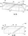
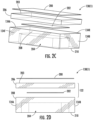
- FIGS 2A-2D are views of a lid 130(1) with an external top conductive layer 200 and an internal conductive layer 202.
- the lid 130(1) forms an air cavity 204 to house the die 118 (e.g., semiconductor).
- the lid 130(1) is of a generally rectangular shape, the lid 130(1) may be any of a variety of shapes and/or sizes.
- Use of air-cavity packages in a transceiver enables higher levels of integration and lower cost assembly methods, such as compared to chip-and-wire microwave module assemblies. As operation frequency increases, package lid effects can introduce cavity-related isolation issues that can lead to performance degradation and/or oscillation issues.
- the lid 130(1) in this and other embodiments discussed herein may not be grounded.
- the external top conductive layer 200 is at a top surface 203 of the lid 130(1).
- the external top conductive layer 200 may be any of a variety of sizes and/or shapes.
- the external top conductive layer 200 may be thicker or thinner.
- the external top conductive layer 200 may cover only a portion of the top surface 203 of the lid 130(1).
- the top wall 132 includes an upper dielectric layer 206 and a lower dielectric layer 208 with the internal conductive layer 202 positioned therebetween.
- the internal conductive layer 202 is embedded within the dielectric layers 206, 208 such that the internal conductive layer 202 is surrounded by dielectric material (e.g., fiber glass).
- the width of the internal conductive layer 202 is less than the width and/or length of the lid 130(1).
- the lid 130(1) may include additional internal conductive layers 202.
- the internal conductive layer 202 may be any size and/or shape.
- the internal conductive layer 202 may be smaller than the external top conductive layer 200.
- the lid 130 includes left sidewall 134A, right sidewall 134B, front sidewall 134F, and rear sidewall 134R (referred to generally as sidewalls 134).
- the sidewalls 134 comprise dielectric material and are devoid of conductive layers 202.
- a bottom surface 210 of the sidewalls 134 is a dielectric material and is devoid of a conductive material. This facilitates application of the lid 130(1) to the carrier 102.
- the dielectric material of the top wall 132 and/or sidewalls 134 includes an epoxy.
- the conductive material of the external top conductive layer 200 and/or the internal conductive layer 202 includes metal.
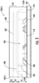
- FIG 3 is a side view of an electronic package 100(1) (i.e., electronic component) with the lid 130(1) of Figures 2A-2D .
- the electronic package 100(1) e.g., transceiver, monolithic microwave integrated circuit (MMIC), etc.
- the electronic package 100(1) includes a carrier 102, a lid 130(1) attached to the carrier 102, and a die 118 (e.g., semiconductor) housed in an air cavity 204 of the lid 130(1).
- An air gap 304 is formed between the die 118 and a top wall 132 of the lid 130(1).
- the die 118 includes an input end 300 and an output end 302.
- the lid 130(1) may inadvertently form a feedback signal path 306 from the output end 302 of the die 118 to the input end 300 of the die 118. This feedback may distort or negatively affect performance of the die 118.
- Use of an external top conductive layer 200 and/or an internal conductive layer 202 is configured to suppress the feedback signal through the feedback signal path 306 to improve performance of the die 118.
- the external top conductive layer 200 and/or the internal conductive layer 202 are not electrically grounded.
- the external top conductive layer 200 and/or the internal conductive layer 202 extend between an input end 300 of the die 118 to an output end 302 of the die 118.
- a user can intentionally tune the frequency response of the electronic package 100(1) by adding conductive layers 200, 202 and/or dielectric layers 206, 208 to the lid 130(1). Doing so can reduce undesirable resonance and feedback in the air cavity 204 and through the lid 130(1).
- Feedback signal suppression performance may be tuned by adjusting the location, size, and/or shape of the external top conductive layer 200, the internal conductive layer 202, and/or the air cavity 204. For example, the width, length, and/or thickness of the internal conductive layer 202 may be altered. Further, a height H1 of the air cavity 204, a height H2 of the internal conductive layer 202 to the air cavity 204, and/or a height H3 of the internal conductive layer 202 from the top surface 203 may be altered.
- the internal conductive layer 202 may be exposed to the air cavity 204 such that only a portion of the internal conductive layer 202 is sandwiched between the dielectric layers 206, 208. In this way, the feedback signal is altered as it propagates through the feedback signal path 306 through the top wall 132 of the lid 130(1).
- Such a configuration is compatible with high volume air cavity package manufacturing processes.
- Figure 4 is a chart illustrating an improvement in feedback signal suppression of the lid 130(1) of Figures 2A-3 .
- the lid 130(1) with the conductive layer 202 improved suppression of the feedback signal, and thereby improved performance of the electronic package 100(1).
- the lid 130(1) suppresses the feedback signal level by 10dB at 40.5 GHz compared to a conventional lid.
- Figure 5 is a perspective view of a lid 130(2) of an electronic package 100(2) with an external top conductive layer 200(2) over only a portion of a top wall 132 of the lid 130(2).
- the external top conductive layer 200(2) only covers a portion of a top surface 203 of the top wall 132.
- the external top conductive layer 200(2) and/or an internal conductive layer 202 are positioned over an output end 302 of a die 118.
- the external top conductive layer 200(2) covers only about 50% of the top surface 203 of the lid 130(2). In certain embodiments, the external top conductive layer 200(2) covers less than 50% of the top surface 203 of the lid 130(2).
- Figure 6 is a side view of a lid 130(3) with multiple internal conductive layers 202(3).
- the plurality of internal conductive layers 202(3) are separated from each other by dielectric material of a top wall 132 of the lid 130(3). Any number of conductive layers 202(3) may be used.
- Figures 7A-7B are views of an electronic package 100(4) with a lid 130(4) with an internal wall 700 extending between an input end 300 and an output end 302 of a semiconductor die 118 in the lid 130(4).
- the electronic package 100(4) includes two dies 118(1), 118(2), each with an input end 300 and an output end 302. It is noted that the input ends 300 of the dies 118(1), 118(2) are in line and adjacent to one another, and the output ends 302 of the dies 118(1), 118(2) are also in line and adjacent to each other. Of course, fewer or more dies 118(1), 118(2) may be used.
- the lid 130(4) includes a top wall 132 and sidewalls 134 extending downwardly from a periphery of the top wall 132.
- the lid 130(4) further includes the downwardly extending internal wall 700.
- the internal wall 700 extends between a front sidewall 134(3) and a rear sidewall 134(4). Accordingly, the internal wall 700 separates an air cavity 204 into a first portion 702(1) proximate the left sidewall 134(1) and a second portion 702(2) proximate the right sidewall 134(2). Further, the internal wall 700 may be offset from a center of the lid 130(4).
- the internal wall 700 is configured to be positioned between the input ends 300 of the dies 118(1), 118(2) and the output ends 302 of the dies 118(1), 118(2).
- the lid has a height of 2 mm to 6 mm, or a height of at least 4 mm.
- a clearance is provided between a bottom 706 of the internal wall 700 and a top 708 of the dies 118(1), 118(2).
- the clearance is between 0.5 mm and 1.5 mm (e.g., 0.9 mm).
- use of the internal wall 700 improves isolation in band by 7 dB.
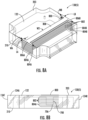
- FIGS 8A-8B are views of a lid 130(5) with conductive layers embedded within the internal wall 700.
- the lid 130(5) includes an external top conductive layer 800 and internal conductive layers 802.
- the top wall 132, sidewalls 134, and/or the internal wall 700 include a dielectric material (e.g., fiberglass).
- the external top conductive layer 800 is at a top surface 203 of the lid 130(5).
- the external top conductive layer 800 may be any of a variety of sizes and/or shapes.
- the external top conductive layer 800 may be thicker or thinner.
- the external top conductive layer 800 may cover only a portion of the top surface 203 of the lid 130(5).
- the internal conductive layers 802 are embedded within the internal wall 700 and/or the sidewalls 134 such that the internal conductive layers 802 are surrounded by dielectric material (e.g., fiber glass).
- the internal conductive layers 802 may be any size and/or shape.
- internal sidewall conductive layers 804A, 804B are embedded within the sidewalls 134.
- the internal conductive layers 802 within the internal wall 700 are positioned between the external top layer 800 and the internal sidewall conductive layers 804A, 804B. In this way, the internal sidewall conductive layers 804A, 804B are positioned proximate a bottom 706 of the internal wall 700 of the lid 130(5).
- Each of the external top conductive layer 800 and/or the plurality of internal conductive layers 802, 804A, 804B are not electrically grounded and/or separated from each other by dielectric material of the top wall 132 and/or sidewalls 134 of the lid 130(5).
- Use of the conductive layers 800, 802, 804A, 804B is to modify and guide a feedback signal through the lid 130(5).
- each of the external top conductive layer 800 and/or internal conductive layers 802 include a left wide sidewall portion 806A, a right wide sidewall portion 806B, and a narrow portion 808 (may also be referred to as a narrow internal wall portion) extending therebetween.
- the left wide sidewall portion 806A and the right wide sidewall portion 806B have a width WA, WB
- the narrow portion 808 has a width W2, where WA, WB are greater than W2.
- the left wide sidewall portion 806A and the right wide sidewall portion 806B have a length LA, LB.
- the internal sidewall conductive layers 804A, 804B are embedded within sidewalls 134A, 134B.
- a first internal sidewall conductive layer 804A is separated from a second internal sidewall conductive layer 804B.
- the internal sidewall conductive layers 804A, 804B may be used to direct the feedback signal downward to the bottom 706 and the periphery of the lid 130(5).
- feedback signal suppression performance may be tuned by adjusting the location, size, and/or shape of the external top conductive layer 800 and the internal conductive layers 802, 804A, 804B. Of course more or fewer layers 802, 804A, 804B may be used. In certain embodiments, isolation is improved by 20 dB.
- Figure 9 is a chart comparing performance of various lids in suppressing feedback signals.
- a conventional lid 900 with a high profile lid 902, with a metal embedded lid 904, with an electronic package without a lid 906, and with an internal wall lid 908.
- the metal embedded lid 904 performed best within the frequency range of interest, followed by the internal wall lid 908.
- the electronic device includes a lid having at least one sidewall and a top wall, as well as a semiconductor positioned within a cavity of the lid.
- the lid includes at least one dielectric material and at least one internal conductive layer at least partially embedded within the at least one dielectric material.
- the lid includes dielectric material, as well as an internal wall extending from the top wall and positioned between an input port and an output port of the semiconductor. Such configurations may suppress any undesirable feedback through the lid between the input port and the output port of the semiconductor.
Landscapes
- Structures Or Materials For Encapsulating Or Coating Semiconductor Devices Or Solid State Devices (AREA)
- Physics & Mathematics (AREA)
- Health & Medical Sciences (AREA)
- Electromagnetism (AREA)
- Toxicology (AREA)
Abstract
Description
- The present teachings relate to packaging of integrated circuits (ICs). In particular, but not exclusively, the present teachings relate to an electronic device with a lid to manage radiation feedback.
- Wireless communication demands often require higher operating frequencies, increased operating power, wider operating and video bandwidths, and/or higher order modulation schemes, etc. A power amplifier is a significant integrated circuit (IC) in these systems. The simultaneous need for more bandwidth, output power, and linearity of the power amplifier are competing requirements. In addition, packaging plays a crucial role in the power amplifier meeting these requirements. For example, performance may be affected by various assembly related variables, such as wirebond length, off-chip component placement, and/or signal/port interface locations relative to an IC.
- Particular aspects are set out in the appended independent claims. Various optional embodiments are set out in the dependent claims.
- Embodiments of the disclosure are directed to an electronic device with a lid to manage radiation feedback. The electronic device includes a lid having at least one sidewall and a top wall, as well as a semiconductor positioned within a cavity of the lid. In certain embodiments, the lid includes at least one dielectric material and at least one internal conductive layer at least partially embedded within the at least one dielectric material. In certain embodiments, the lid includes dielectric material, as well as an internal wall extending from the top wall and positioned between an input port and an output port of the semiconductor. Such configurations may suppress any undesirable feedback through the lid between the input port and output port of the semiconductor.
- One embodiment of the disclosure relates to an electronic package including a lid defining a cavity. The lid includes at least one sidewall and a top wall including at least one dielectric material and at least one internal conductive layer at least partially embedded within the at least one dielectric material, the at least one dielectric material comprising epoxy. The electronic package further includes a semiconductor positioned within the cavity of the lid.
- Another embodiment of the disclosure relates to an electronic package including a lid defining a cavity. The lid includes at least one sidewall, a top wall comprising at least one dielectric material, and an internal wall extending from the top wall. The internal wall includes at least one dielectric material. The electronic package includes at least one semiconductor positioned within the cavity of the lid. The at least one semiconductor includes at least one input port and at least one output port. The internal wall is positioned between the at least one input port and the at least one output port.
- Those skilled in the art will appreciate the scope of the present disclosure and realize additional aspects thereof after reading the following detailed description of the example embodiments in association with the accompanying drawing figures.
- The accompanying drawing figures incorporated in and forming a part of this specification illustrate several aspects of the disclosure, and together with the description, serve to explain the principles of the disclosure.
-
Figure 1A is a top perspective exploded view of an electronic package (e.g., semiconductor package). -
Figure 1B is a cross-sectional side view of the electronic package ofFigure 1A . -
Figure 2A is an assembled perspective view of a lid with a top conductive layer and an internal conductive layer. -
Figure 2B is an cross-sectional sideview ofFigure 2A . -
Figure 2C is an exploded perspective view of the lid ofFigure 2A . -
Figure 2D is an exploded cross-sectional sideview of the lid ofFigure 2B . -
Figure 3 is a side view of an electronic package with the lid ofFigures 2A- 2D. -
Figure 4 is a chart illustrating an improvement in feedback signal suppression of the lid ofFigures 2A-3 . -
Figure 5 is a perspective view of a lid with a top conductive layer over only a portion of a top wall of the lid. -
Figure 6 is a side view of a lid with multiple internal conductive layers. -
Figure 7A is a top view of an electronic package with a lid with an internal wall extending between an input port and an output port of a semiconductor die in the lid. -
Figure 7B is a perspective view of the lid ofFigure 7A . -
Figure 8A is a perspective view of a lid with conductive layers embedded within the internal wall. -
Figure 8B is a side view of the lid ofFigure 8A . -
Figure 9 is a chart comparing performance of various lids in suppressing feedback signals. - The embodiments set forth below represent the necessary information to enable those skilled in the art to practice the embodiments and illustrate the best mode of practicing the embodiments. Upon reading the following description in light of the accompanying drawing figures, those skilled in the art will understand the concepts of the disclosure and will recognize applications of these concepts not particularly addressed herein. It should be understood that these concepts and applications fall within the scope of the disclosure and the accompanying claims.
- It should be understood that, although the terms first, second, etc., may be used herein to describe various elements, these elements should not be limited by these terms. These terms are only used to distinguish one element from another. For example, a first element could be termed a second element, and, similarly, a second element could be termed a first element without departing from the scope of the present disclosure. As used herein, the term "and/or" includes any and all combinations of one or more of the associated listed items.
- It should also be understood that when an element is referred to as being "connected" or "coupled" to another element, it can be directly connected or coupled to the other element, or intervening elements may be present. In contrast, when an element is referred to as being "directly connected" or "directly coupled" to another element, there are no intervening elements present.
- It should be understood that, although the terms "upper," "lower," "bottom," "intermediate," "middle," "top," and the like may be used herein to describe various elements, these elements should not be limited by these terms. These terms are only used to distinguish one element from another. For example, a first element could be termed an "upper" element, and, similarly, a second element could be termed an "upper" element depending on the relative orientations of these elements, without departing from the scope of the present disclosure.
- The terminology used herein is for the purpose of describing particular embodiments only and is not intended to be limiting of the disclosure. As used herein, the singular forms "a," "an," and "the" are intended to include the plural forms as well, unless the context clearly indicates otherwise. It will be further understood that the terms "comprises," "comprising," "includes," and/or "including" when used herein specify the presence of stated features, integers, steps, operations, elements, and/or components, but do not preclude the presence or addition of one or more other features, integers, steps, operations, elements, components, and/or groups thereof.
- Unless otherwise defined, all terms (including technical and scientific terms) used herein have the same meaning as commonly understood by one of ordinary skill in the art to which this disclosure belongs. It will be further understood that terms used herein should be interpreted as having meanings that are consistent with their meanings in the context of this specification and the relevant art and will not be interpreted in an idealized or overly formal sense unless expressly so defined herein.
- Embodiments of the disclosure are directed to an electronic device with a lid to manage radiation feedback. The electronic device includes a lid having at least one sidewall and a top wall, as well as a semiconductor positioned within a cavity of the lid. In certain embodiments, the lid includes at least one dielectric material and at least one internal conductive layer at least partially embedded within the at least one dielectric material. In certain embodiments, the lid includes dielectric material, as well as an internal wall extending from the top wall and positioned between an input port and an output port of the semiconductor. Such configurations may suppress any undesirable feedback through the lid between the input port and output port of the semiconductor.
- Before delving into specific details of various aspects of the present disclosure, an overview of various elements that may be included in example electronic packages of the present disclosure is provided. In particular,
Figures 1A-1B are views of an electronic package 100 (may also be referred to as a semiconductor package 100). - The
electronic package 100 may include a carrier 102 (may also be referred to as a base). In certain embodiments, thecarrier 102 may be sufficiently rigid so as to prevent undesired flexing of any components coupled thereto. Additionally, thecarrier 102 may include a plurality ofholes 104 suitable for receiving a fastening means, such as screws or pins. Theholes 104 may allow theelectronic package 100 to be affixed to a host device or system, such as a radio frequency (RF) system. Thecarrier 102 may be formed from electrically conductive materials, thermally conductive materials, or non-conductive materials. In certain embodiments, thecarrier 102 may include metal, metal alloy, ceramic, diamond, copper, tungsten, tungsten-copper (W-Cu), and/or copper-molybdenum-copper (Cu-Mo-Cu). In other embodiments, thecarrier 102 may be plated, such as with a conductive material (e.g., gold). - The
electronic package 100 may include a ring structure 106 (may also be referred to as a signal carrying component, ring frame, etc.), which may be a printed circuit board (PCB), laminate, substrate, printed wiring board, flexible circuit, dielectric (e.g., soft dielectric), and/or or another similar component comprising conductive pathways. Thering structure 106 may be coupled to thecarrier 102, such as by an adhesive material (e.g., epoxy), soldering, pressure bonding, and/or temperature bonding. In certain embodiments, an adhesive material used to attach thering structure 106 to thecarrier 102 may be conductive, such as a conductive epoxy preform. - The
ring structure 106 has anopening 108 therethrough. In certain embodiments, thering structure 106 may have a plurality ofouter pads 110, which may be made of a conductive material (e.g., copper). Theouter pads 110 may be adapted to have one or more components (e.g., active and/or passive components) and/or leads attached thereto (e.g., via soldering).Interconnects 112 may be attached to theouter pads 110 of thering structure 106, such as through conventional ribbon or wire bonding techniques. - In some embodiments, the
ring structure 106 of theelectronic package 100 may be coupled to one or more leads 114, 116 that carry a signal through theelectronic package 100. Theelectronic package 100 may include input-side leads 114 located at a first side (e.g., input side) of the electronic package 100 (e.g., to receive RF input signals). Output-side leads 116 are leads located at a second side (e.g., output side) of theelectronic package 100, on which theelectronic package 100 may provide output signals to an external circuitry/system. Each of the input-side leads 114 and/or output-side leads 116 may be formed of a metal or metal alloy, such as copper. The plurality ofleads - The
electronic package 100 may include one or more dies 118 and/or one or moreelectronic components 120 attached to thecarrier 102 and disposed in theopening 108 of thering structure 106, such that thering structure 106 surrounds the at least onedie 118 and/or theelectronic components 120. Thedie 118 and/or theelectronic components 120 may be mechanically coupled to thecarrier 102 via solder 128 (e.g., gold-tin, or other alloys) and/or another die attach. - The
ring structure 106 may be electrically coupled to the die 118 through theinterconnects 112. Thedie 118 may have a functional circuit fabricated thereon. Thedie 118 may include gallium arsenide (GaAs), gallium nitride (GaN), etc. Thedie 118 may be attached using any suitable material, such as gold-tin (AuSn) or another alloy. In certain embodiments, thedie 118 includes diepads 124 on a top surface of thedie 118, each of which is connected to a corresponding connectingtrace 126 via aninterconnect 112, such as a wire or a ribbon bond. The connecting traces 126 and thedie pads 124 may be formed of any suitably conductive material, such as copper. - The one or more
electronic components 120 may be attached directly to thecarrier 102, and/or attached to thering structure 106. The one or moreelectronic components 120 may include active components (e.g., transistors, diodes, and the like) and/or passive components (e.g., resistors, capacitors, inductors, transformers, and the like). The one or more of theelectronic components 120 may be electrically coupled to thering structure 106 via one or more of theinterconnects 112. - A
lid 130 may have atop wall 132 and a plurality ofsidewalls 134 attached to thering structure 106. Thus, thecarrier 102, thering structure 106, the input-side leads 114, the output-side leads 116, and thelid 130 may enclose thedie 118 and theelectronic components 120 in theelectronic package 100. Thelid 130 may be formed from plastic, a plastic composite material, metal, metal alloy, and/or ceramic, etc. Thelid 130 may be coupled to a top surface of the ring structure 106 (e.g., a surface opposite the surface of thering structure 106 that is coupled to the carrier 102), such as by an adhesive material (e.g., epoxy, resin, acrylic, and/or silicone). Thelid 130 may be coupled directly to thecarrier 102 in some embodiments. In certain embodiments, the adhesive material used to attach thelid 130 to thering structure 106 or to thecarrier 102 may be non-conductive. As part of the enclosure provided by theelectronic package 100, a seal ring may be formed, for example, to protect elements (e.g., a die, active components, and/or passive components) sealed in by the combination of thecarrier 102, thering structure 106, and thelid 130. -
Figures 2A-2D are views of a lid 130(1) with an external topconductive layer 200 and an internalconductive layer 202. In particular, the lid 130(1) forms anair cavity 204 to house the die 118 (e.g., semiconductor). Although the lid 130(1) is of a generally rectangular shape, the lid 130(1) may be any of a variety of shapes and/or sizes. Use of air-cavity packages in a transceiver enables higher levels of integration and lower cost assembly methods, such as compared to chip-and-wire microwave module assemblies. As operation frequency increases, package lid effects can introduce cavity-related isolation issues that can lead to performance degradation and/or oscillation issues. The lid 130(1) in this and other embodiments discussed herein may not be grounded. - The external top
conductive layer 200 is at atop surface 203 of the lid 130(1). The external topconductive layer 200 may be any of a variety of sizes and/or shapes. For example, the external topconductive layer 200 may be thicker or thinner. The external topconductive layer 200 may cover only a portion of thetop surface 203 of the lid 130(1). - The
top wall 132 includes anupper dielectric layer 206 and a lowerdielectric layer 208 with the internalconductive layer 202 positioned therebetween. The internalconductive layer 202 is embedded within thedielectric layers conductive layer 202 is surrounded by dielectric material (e.g., fiber glass). The width of the internalconductive layer 202 is less than the width and/or length of the lid 130(1). In certain embodiments, the lid 130(1) may include additional internalconductive layers 202. Further, the internalconductive layer 202 may be any size and/or shape. For example, the internalconductive layer 202 may be smaller than the external topconductive layer 200. - The
lid 130 includes left sidewall 134A,right sidewall 134B,front sidewall 134F, andrear sidewall 134R (referred to generally as sidewalls 134). In certain embodiments, thesidewalls 134 comprise dielectric material and are devoid ofconductive layers 202. In particular, abottom surface 210 of thesidewalls 134 is a dielectric material and is devoid of a conductive material. This facilitates application of the lid 130(1) to thecarrier 102. - In certain embodiments, the dielectric material of the
top wall 132 and/orsidewalls 134 includes an epoxy. The conductive material of the external topconductive layer 200 and/or the internalconductive layer 202 includes metal. -
Figure 3 is a side view of an electronic package 100(1) (i.e., electronic component) with the lid 130(1) ofFigures 2A-2D . In particular, the electronic package 100(1) (e.g., transceiver, monolithic microwave integrated circuit (MMIC), etc.) includes acarrier 102, a lid 130(1) attached to thecarrier 102, and a die 118 (e.g., semiconductor) housed in anair cavity 204 of the lid 130(1). Anair gap 304 is formed between the die 118 and atop wall 132 of the lid 130(1). Thedie 118 includes aninput end 300 and anoutput end 302. The lid 130(1) may inadvertently form afeedback signal path 306 from theoutput end 302 of the die 118 to theinput end 300 of thedie 118. This feedback may distort or negatively affect performance of thedie 118. Use of an external topconductive layer 200 and/or an internalconductive layer 202 is configured to suppress the feedback signal through thefeedback signal path 306 to improve performance of thedie 118. In particular, the external topconductive layer 200 and/or the internalconductive layer 202 are not electrically grounded. As shown, in certain embodiments, the external topconductive layer 200 and/or the internalconductive layer 202 extend between aninput end 300 of the die 118 to anoutput end 302 of thedie 118. - A user can intentionally tune the frequency response of the electronic package 100(1) by adding
conductive layers dielectric layers air cavity 204 and through the lid 130(1). Feedback signal suppression performance may be tuned by adjusting the location, size, and/or shape of the external topconductive layer 200, the internalconductive layer 202, and/or theair cavity 204. For example, the width, length, and/or thickness of the internalconductive layer 202 may be altered. Further, a height H1 of theair cavity 204, a height H2 of the internalconductive layer 202 to theair cavity 204, and/or a height H3 of the internalconductive layer 202 from thetop surface 203 may be altered. In certain embodiments, the internalconductive layer 202 may be exposed to theair cavity 204 such that only a portion of the internalconductive layer 202 is sandwiched between thedielectric layers feedback signal path 306 through thetop wall 132 of the lid 130(1). Such a configuration is compatible with high volume air cavity package manufacturing processes. -
Figure 4 is a chart illustrating an improvement in feedback signal suppression of the lid 130(1) ofFigures 2A-3 . As illustrated, the lid 130(1) with theconductive layer 202 improved suppression of the feedback signal, and thereby improved performance of the electronic package 100(1). For example, in certain embodiments, the lid 130(1) suppresses the feedback signal level by 10dB at 40.5 GHz compared to a conventional lid. -
Figure 5 is a perspective view of a lid 130(2) of an electronic package 100(2) with an external top conductive layer 200(2) over only a portion of atop wall 132 of the lid 130(2). As illustrated, the external top conductive layer 200(2) only covers a portion of atop surface 203 of thetop wall 132. In certain embodiments, the external top conductive layer 200(2) and/or an internalconductive layer 202 are positioned over anoutput end 302 of adie 118. In certain embodiments, the external top conductive layer 200(2) covers only about 50% of thetop surface 203 of the lid 130(2). In certain embodiments, the external top conductive layer 200(2) covers less than 50% of thetop surface 203 of the lid 130(2). -
Figure 6 is a side view of a lid 130(3) with multiple internal conductive layers 202(3). In particular, the plurality of internal conductive layers 202(3) are separated from each other by dielectric material of atop wall 132 of the lid 130(3). Any number of conductive layers 202(3) may be used. -
Figures 7A-7B are views of an electronic package 100(4) with a lid 130(4) with aninternal wall 700 extending between aninput end 300 and anoutput end 302 of asemiconductor die 118 in the lid 130(4). The electronic package 100(4) includes two dies 118(1), 118(2), each with aninput end 300 and anoutput end 302. It is noted that the input ends 300 of the dies 118(1), 118(2) are in line and adjacent to one another, and the output ends 302 of the dies 118(1), 118(2) are also in line and adjacent to each other. Of course, fewer or more dies 118(1), 118(2) may be used. - The lid 130(4) includes a
top wall 132 andsidewalls 134 extending downwardly from a periphery of thetop wall 132. The lid 130(4) further includes the downwardly extendinginternal wall 700. Theinternal wall 700 extends between a front sidewall 134(3) and a rear sidewall 134(4). Accordingly, theinternal wall 700 separates anair cavity 204 into a first portion 702(1) proximate the left sidewall 134(1) and a second portion 702(2) proximate the right sidewall 134(2). Further, theinternal wall 700 may be offset from a center of the lid 130(4). In particular, theinternal wall 700 is configured to be positioned between the input ends 300 of the dies 118(1), 118(2) and the output ends 302 of the dies 118(1), 118(2). - As similarly noted above, use of air-cavity packages in a transceiver enables higher levels of integration and lower cost assembly methods, such as compared to chip-and-wire microwave module assemblies. As operation frequency increases, package lid effects can introduce cavity-related isolation issues that can lead to performance degradation and/or oscillation issues. The
internal wall 700 of the lid 130(4) reduces feedback through the lid, thereby improving frequency response and stability. - In certain embodiments the lid has a height of 2 mm to 6 mm, or a height of at least 4 mm. In certain embodiments, a clearance is provided between a bottom 706 of the
internal wall 700 and a top 708 of the dies 118(1), 118(2). In certain embodiments, the clearance is between 0.5 mm and 1.5 mm (e.g., 0.9 mm). In certain embodiments, use of theinternal wall 700 improves isolation in band by 7 dB. -
Figures 8A-8B are views of a lid 130(5) with conductive layers embedded within theinternal wall 700. In particular, the lid 130(5) includes an external topconductive layer 800 and internalconductive layers 802. As similarly noted above, thetop wall 132,sidewalls 134, and/or theinternal wall 700 include a dielectric material (e.g., fiberglass). The external topconductive layer 800 is at atop surface 203 of the lid 130(5). The external topconductive layer 800 may be any of a variety of sizes and/or shapes. For example, the external topconductive layer 800 may be thicker or thinner. The external topconductive layer 800 may cover only a portion of thetop surface 203 of the lid 130(5). - The internal
conductive layers 802 are embedded within theinternal wall 700 and/or thesidewalls 134 such that the internalconductive layers 802 are surrounded by dielectric material (e.g., fiber glass). The internalconductive layers 802 may be any size and/or shape. Further, internal sidewallconductive layers sidewalls 134. In certain embodiments, the internalconductive layers 802 within theinternal wall 700 are positioned between the externaltop layer 800 and the internal sidewallconductive layers conductive layers internal wall 700 of the lid 130(5). - Each of the external top
conductive layer 800 and/or the plurality of internalconductive layers top wall 132 and/orsidewalls 134 of the lid 130(5). Use of theconductive layers - In certain embodiments, each of the external top
conductive layer 800 and/or internalconductive layers 802 include a leftwide sidewall portion 806A, a rightwide sidewall portion 806B, and a narrow portion 808 (may also be referred to as a narrow internal wall portion) extending therebetween. In this way the leftwide sidewall portion 806A and the rightwide sidewall portion 806B have a width WA, WB, and thenarrow portion 808 has a width W2, where WA, WB are greater than W2. Further, the leftwide sidewall portion 806A and the rightwide sidewall portion 806B have a length LA, LB. - The internal sidewall
conductive layers conductive layer 804A is separated from a second internal sidewallconductive layer 804B. The internal sidewallconductive layers - As similarly discussed above, feedback signal suppression performance may be tuned by adjusting the location, size, and/or shape of the external top
conductive layer 800 and the internalconductive layers fewer layers -
Figure 9 is a chart comparing performance of various lids in suppressing feedback signals. In particular, illustrated is performance of aconventional lid 900, with ahigh profile lid 902, with a metal embeddedlid 904, with an electronic package without alid 906, and with aninternal wall lid 908. As illustrated, the metal embeddedlid 904 performed best within the frequency range of interest, followed by theinternal wall lid 908. - Therefore, from one perspective, there have been described approaches for an electronic device with a lid to manage radiation feedback. The electronic device includes a lid having at least one sidewall and a top wall, as well as a semiconductor positioned within a cavity of the lid. In certain embodiments, the lid includes at least one dielectric material and at least one internal conductive layer at least partially embedded within the at least one dielectric material. In certain embodiments, the lid includes dielectric material, as well as an internal wall extending from the top wall and positioned between an input port and an output port of the semiconductor. Such configurations may suppress any undesirable feedback through the lid between the input port and the output port of the semiconductor.
- Further examples are set out in the following numbered clauses:
-
Clause 1. An electronic package, comprising: a lid defining a cavity, the lid comprising: at least one sidewall; a top wall comprising at least one dielectric material and at least one internal conductive layer at least partially embedded within the at least one dielectric material, the at least one dielectric material comprising epoxy; and a semiconductor positioned within the cavity of the lid. -
Clause 2. The electronic package ofclause 1, wherein the electronic package comprises a transceiver. -
Clause 3. The electronic package ofclause -
Clause 4. The electronic package ofclause -
Clause 5. The electronic package of any ofclauses 1 to 4, wherein the at least one internal conductive layer comprises a metal material. - Clause 6. The electronic package of any of
clauses 1 to 5, wherein the at least one internal conductive layer is not electrically grounded. - Clause 7. The electronic package of any of
clauses 1 to 6, wherein the at least one internal conductive layer extends between an input end of the semiconductor to an output end of the semiconductor. - Clause 8. The electronic package of any of
clauses 1 to 7, wherein the at least one internal conductive layer comprises a plurality of internal conductive layers. - Clause 9. The electronic package of clause 8, wherein the plurality of internal conductive layers are separated from each other by the at least one dielectric material of the top wall of the lid.
- Clause 10. The electronic package of any of
clauses 1 to 9, further comprising at least one external conductive layer over at least a portion of the top wall of the lid. - Clause 11. An electronic package, comprising: a lid defining a cavity, the lid comprising: at least one sidewall; a top wall comprising at least one dielectric material; an internal wall extending from the top wall, the internal wall comprising at least one dielectric material; and at least one semiconductor positioned within the cavity of the lid, the at least one semiconductor comprising at least one input port and at least one output port; wherein the internal wall is positioned between the at least one input port and the at least one output port.
- Clause 12. The electronic package of clause 11, wherein the lid comprises a height of at least 4mm.
- Clause 13. The electronic package of clause 11 or 12, wherein the at least one sidewall comprises two opposing sidewalls, and the internal wall integrally extends between the two opposing sidewalls.
- Clause 14. The electronic package of clause 11, 12 or 13, wherein the at least one semiconductor comprises a first semiconductor and a second semiconductor, each of the first semiconductor and the second semiconductor comprising the at least one input port and the at least one output port; and wherein the internal wall is positioned between: the at least one input port of the first semiconductor and the at least one output port of the first semiconductor; and the at least one input port of the second semiconductor and the at least one output port of the second semiconductor.
- Clause 15. The electronic package of any of clauses 11 to 14, further comprising at least one internal conductive layer embedded within the internal wall.
- Clause 16. The electronic package of clause 15, wherein the at least one internal conductive layer comprises a plurality of internal conductive layers.
- Clause 17. The electronic package of clause 16, wherein the plurality of internal conductive layers are separated from each other by the at least one dielectric material of the top wall of the lid.
- Clause 18. The electronic package of clause 15, 16 or 17, wherein the at least one internal conductive layer comprises a first wide sidewall portion, a second wide sidewall portion, and a narrow internal wall portion extending between the first wide sidewall portion and the second wide sidewall portion.
- Clause 19. The electronic package of any of clauses 15 to 18, wherein the at least one sidewall comprises two opposing sidewalls, and the internal wall integrally extends between the two opposing sidewalls; wherein the at least one internal conductive layer comprises a first internal conductive layer proximate a top of the lid and a second internal conductive layer proximate a bottom of the lid; wherein the first internal conductive layer comprises a first wide sidewall portion within a first sidewall, a second wide sidewall portion within a second sidewall, and a narrow internal wall portion within the internal wall, the narrow internal wall portion extending between the first wide sidewall portion and the second wide sidewall portion; and wherein the second internal conductive layer comprises a first wide sidewall portion within the first sidewall and a second wide sidewall portion within the second sidewall, the first wide sidewall portion of the second internal conductive layer separate from the second wide sidewall portion of the second internal conductive layer.
- Clause 20. The electronic package of any of clauses 11 to 19, further comprising at least one external conductive layer over at least a portion of the top wall of the lid.
- Those skilled in the art will recognize improvements and modifications to the example embodiments of the present disclosure. All such improvements and modifications are considered within the scope of the concepts disclosed herein and the claims that follow.
Claims (15)
- An electronic package, comprising:
a lid defining a cavity, the lid comprising:at least one sidewall;a top wall comprising at least one dielectric material and at least one internal conductive layer at least partially embedded within the at least one dielectric material, the at least one dielectric material comprising epoxy; anda semiconductor positioned within the cavity of the lid. - The electronic package of claim 1, wherein the electronic package comprises a transceiver.
- The electronic package of claim 1 or 2, wherein the electronic package comprises a monolithic microwave integrated circuit (MMIC).
- The electronic package of claim 1, 2 or 3, wherein the lid forms an air gap between the top wall and the semiconductor.
- The electronic package of any of claims 1 to 4, wherein the at least one internal conductive layer comprises at least one property selected from the group comprising: comprising a metal material; being not electrically grounded; and extending between an input end of the semiconductor to an output end of the semiconductor.
- The electronic package of any of claims 1 to 5, wherein the at least one internal conductive layer comprises a plurality of internal conductive layers; and, for example, wherein the plurality of internal conductive layers are separated from each other by the at least one dielectric material of the top wall of the lid.
- The electronic package of any of claims 1 to 6, further comprising at least one external conductive layer over at least a portion of the top wall of the lid.
- An electronic package, comprising:
a lid defining a cavity, the lid comprising:at least one sidewall;a top wall comprising at least one dielectric material;an internal wall extending from the top wall, the internal wall comprising at least one dielectric material; andat least one semiconductor positioned within the cavity of the lid, the at least one semiconductor comprising at least one input port and at least one output port;wherein the internal wall is positioned between the at least one input port and the at least one output port. - The electronic package of claim 8, wherein the lid comprises a height of at least 4mm.
- The electronic package of claim 8 or 9, wherein the at least one sidewall comprises two opposing sidewalls, and the internal wall integrally extends between the two opposing sidewalls.
- The electronic package of claim 8, 9 or 10,wherein the at least one semiconductor comprises a first semiconductor and a second semiconductor, each of the first semiconductor and the second semiconductor comprising the at least one input port and the at least one output port; andwherein the internal wall is positioned between:the at least one input port of the first semiconductor and the at least one output port of the first semiconductor; andthe at least one input port of the second semiconductor and the at least one output port of the second semiconductor.
- The electronic package of any of claims 8 to 11, further comprising at least one internal conductive layer embedded within the internal wall; and for example wherein the at least one internal conductive layer comprises a plurality of internal conductive layers; and for example wherein the plurality of internal conductive layers are separated from each other by the at least one dielectric material of the top wall of the lid.
- The electronic package of claim 12, wherein the at least one internal conductive layer comprises a first wide sidewall portion, a second wide sidewall portion, and a narrow internal wall portion extending between the first wide sidewall portion and the second wide sidewall portion.
- The electronic package of claim 12 or 13,wherein the at least one sidewall comprises two opposing sidewalls, and the internal wall integrally extends between the two opposing sidewalls;wherein the at least one internal conductive layer comprises a first internal conductive layer proximate a top of the lid and a second internal conductive layer proximate a bottom of the lid;wherein the first internal conductive layer comprises a first wide sidewall portion within a first sidewall, a second wide sidewall portion within a second sidewall, and a narrow internal wall portion within the internal wall, the narrow internal wall portion extending between the first wide sidewall portion and the second wide sidewall portion; andwherein the second internal conductive layer comprises a first wide sidewall portion within the first sidewall and a second wide sidewall portion within the second sidewall, the first wide sidewall portion of the second internal conductive layer separate from the second wide sidewall portion of the second internal conductive layer.
- The electronic package of any of claims 8 to 14, further comprising at least one external conductive layer over at least a portion of the top wall of the lid.
Applications Claiming Priority (1)
| Application Number | Priority Date | Filing Date | Title |
|---|---|---|---|
| US17/557,551 US11948893B2 (en) | 2021-12-21 | 2021-12-21 | Electronic component with lid to manage radiation feedback |
Publications (2)
| Publication Number | Publication Date |
|---|---|
| EP4203006A2 true EP4203006A2 (en) | 2023-06-28 |
| EP4203006A3 EP4203006A3 (en) | 2023-07-05 |
Family
ID=84439830
Family Applications (1)
| Application Number | Title | Priority Date | Filing Date |
|---|---|---|---|
| EP22211991.9A Pending EP4203006A3 (en) | 2021-12-21 | 2022-12-07 | Electronic component with lid to manage radiation feedback |
Country Status (3)
| Country | Link |
|---|---|
| US (3) | US11948893B2 (en) |
| EP (1) | EP4203006A3 (en) |
| CN (1) | CN116314037A (en) |
Families Citing this family (2)
| Publication number | Priority date | Publication date | Assignee | Title |
|---|---|---|---|---|
| US12136615B2 (en) * | 2021-11-30 | 2024-11-05 | Qorvo Us, Inc. | Electronic package with interposer between integrated circuit dies |
| US11948893B2 (en) | 2021-12-21 | 2024-04-02 | Qorvo Us, Inc. | Electronic component with lid to manage radiation feedback |
Family Cites Families (13)
| Publication number | Priority date | Publication date | Assignee | Title |
|---|---|---|---|---|
| WO1996027282A1 (en) | 1995-03-02 | 1996-09-06 | Circuit Components Incorporated | A low cost, high performance package for microwave circuits in the up to 90 ghz frequency range using bga i/o rf port format and ceramic substrate technology |
| US6730991B1 (en) * | 1996-06-11 | 2004-05-04 | Raytheon Company | Integrated circuit chip package |
| US7813145B2 (en) * | 2004-06-30 | 2010-10-12 | Endwave Corporation | Circuit structure with multifunction circuit cover |
| EP1795498A3 (en) | 2005-12-06 | 2011-05-11 | Yamaha Corporation | Package for a semiconductor device |
| US8093691B1 (en) | 2009-07-14 | 2012-01-10 | Amkor Technology, Inc. | System and method for RF shielding of a semiconductor package |
| JP5231382B2 (en) * | 2009-11-27 | 2013-07-10 | 新光電気工業株式会社 | Semiconductor device |
| JP5521862B2 (en) | 2010-07-29 | 2014-06-18 | 三菱電機株式会社 | Manufacturing method of semiconductor device |
| US9899292B2 (en) * | 2016-02-05 | 2018-02-20 | Qorvo Us, Inc. | Top-side cooling of RF products in air cavity composite packages |
| US10068817B2 (en) * | 2016-03-18 | 2018-09-04 | Macom Technology Solutions Holdings, Inc. | Semiconductor package |
| US9960127B2 (en) * | 2016-05-18 | 2018-05-01 | Macom Technology Solutions Holdings, Inc. | High-power amplifier package |
| US20190259676A1 (en) | 2018-02-21 | 2019-08-22 | Bae Systems Information And Electronic Systems Integration Inc. | Iii-v chip-scale smt package |
| JP7260662B2 (en) * | 2019-10-29 | 2023-04-18 | 京セラ株式会社 | Lid body, electronic component storage package, and electronic device |
| US11948893B2 (en) | 2021-12-21 | 2024-04-02 | Qorvo Us, Inc. | Electronic component with lid to manage radiation feedback |
-
2021
- 2021-12-21 US US17/557,551 patent/US11948893B2/en active Active
-
2022
- 2022-12-07 EP EP22211991.9A patent/EP4203006A3/en active Pending
- 2022-12-21 CN CN202211648140.0A patent/CN116314037A/en active Pending
-
2024
- 2024-03-01 US US18/592,693 patent/US12308326B2/en active Active
-
2025
- 2025-02-25 US US19/062,281 patent/US20250201728A1/en active Pending
Also Published As
| Publication number | Publication date |
|---|---|
| US12308326B2 (en) | 2025-05-20 |
| CN116314037A (en) | 2023-06-23 |
| US20230197629A1 (en) | 2023-06-22 |
| US11948893B2 (en) | 2024-04-02 |
| US20240250041A1 (en) | 2024-07-25 |
| US20250201728A1 (en) | 2025-06-19 |
| EP4203006A3 (en) | 2023-07-05 |
Similar Documents
| Publication | Publication Date | Title |
|---|---|---|
| US20250201728A1 (en) | Electronic component with lid to manage radiation feedback | |
| KR100993277B1 (en) | Semiconductor device and electronic device | |
| EP0595346B1 (en) | Composite microwave module assembly and its connection structure | |
| US7268426B2 (en) | High-frequency chip packages | |
| EP0766410B1 (en) | Ultra high frequency radio communication apparatus | |
| US8901719B2 (en) | Transition from a chip to a waveguide port | |
| JP7565365B2 (en) | DEVICE CARRIER CONFIGURED FOR INTERCONNECTING, PACKAGE MOUNTING DEVICE CARRIER HAVING INTERCONNECTING, AND METHOD OF MANUFACTURING SAME - Patent application | |
| EP4128341B1 (en) | Multi-chip package with reinforced isolation | |
| US9142492B2 (en) | Leadframe package with integrated partial waveguide interface | |
| EP2600396B1 (en) | Electronic component housing unit, electronic module and electronic device | |
| US6072238A (en) | Semiconductor component | |
| KR100993579B1 (en) | Semiconductor device and electronic device | |
| EP4210102A1 (en) | Electronic package with interposer between integrated circuit dies | |
| JP7275177B2 (en) | Radio frequency package mounting window frame with edge plating and process for mounting same | |
| US9252767B1 (en) | Integrated switch module | |
| JPH11195731A (en) | Semiconductor device | |
| CN100536123C (en) | Semiconductor device and electronic device | |
| KR102648997B1 (en) | Guide type flange package and method of manufacturing the same | |
| WO2023053228A1 (en) | Semiconductor device | |
| KR20240117634A (en) | IPD components with SIC substrates and devices and processes implementing them | |
| JPWO1996012296A1 (en) | Semiconductor device and manufacturing method thereof |
Legal Events
| Date | Code | Title | Description |
|---|---|---|---|
| PUAI | Public reference made under article 153(3) epc to a published international application that has entered the european phase |
Free format text: ORIGINAL CODE: 0009012 |
|
| REG | Reference to a national code |
Ref country code: DE Ref legal event code: R079 Free format text: PREVIOUS MAIN CLASS: H01L0023020000 Ipc: H01L0023552000 |
|
| STAA | Information on the status of an ep patent application or granted ep patent |
Free format text: STATUS: THE APPLICATION HAS BEEN PUBLISHED |
|
| PUAL | Search report despatched |
Free format text: ORIGINAL CODE: 0009013 |
|
| AK | Designated contracting states |
Kind code of ref document: A2 Designated state(s): AL AT BE BG CH CY CZ DE DK EE ES FI FR GB GR HR HU IE IS IT LI LT LU LV MC ME MK MT NL NO PL PT RO RS SE SI SK SM TR |
|
| AK | Designated contracting states |
Kind code of ref document: A3 Designated state(s): AL AT BE BG CH CY CZ DE DK EE ES FI FR GB GR HR HU IE IS IT LI LT LU LV MC ME MK MT NL NO PL PT RO RS SE SI SK SM TR |
|
| RIC1 | Information provided on ipc code assigned before grant |
Ipc: H01L 23/485 20060101ALN20230526BHEP Ipc: H01L 23/66 20060101ALN20230526BHEP Ipc: H01L 23/02 20060101ALI20230526BHEP Ipc: H01L 23/552 20060101AFI20230526BHEP |
|
| STAA | Information on the status of an ep patent application or granted ep patent |
Free format text: STATUS: REQUEST FOR EXAMINATION WAS MADE |
|
| 17P | Request for examination filed |
Effective date: 20240105 |
|
| RBV | Designated contracting states (corrected) |
Designated state(s): AL AT BE BG CH CY CZ DE DK EE ES FI FR GB GR HR HU IE IS IT LI LT LU LV MC ME MK MT NL NO PL PT RO RS SE SI SK SM TR |
|
| RAP3 | Party data changed (applicant data changed or rights of an application transferred) |
Owner name: QORVO US, INC. |