EP4202552A1 - Method and structure for determining an overlay error - Google Patents
Method and structure for determining an overlay error Download PDFInfo
- Publication number
- EP4202552A1 EP4202552A1 EP21217706.7A EP21217706A EP4202552A1 EP 4202552 A1 EP4202552 A1 EP 4202552A1 EP 21217706 A EP21217706 A EP 21217706A EP 4202552 A1 EP4202552 A1 EP 4202552A1
- Authority
- EP
- European Patent Office
- Prior art keywords
- layer
- masking
- distance
- top surface
- feature
- Prior art date
- Legal status (The legal status is an assumption and is not a legal conclusion. Google has not performed a legal analysis and makes no representation as to the accuracy of the status listed.)
- Granted
Links
Images


Classifications
-
- H—ELECTRICITY
- H10—SEMICONDUCTOR DEVICES; ELECTRIC SOLID-STATE DEVICES NOT OTHERWISE PROVIDED FOR
- H10P—GENERIC PROCESSES OR APPARATUS FOR THE MANUFACTURE OR TREATMENT OF DEVICES COVERED BY CLASS H10
- H10P74/00—Testing or measuring during manufacture or treatment of wafers, substrates or devices
- H10P74/20—Testing or measuring during manufacture or treatment of wafers, substrates or devices characterised by the properties tested or measured, e.g. structural or electrical properties
- H10P74/203—Structural properties, e.g. testing or measuring thicknesses, line widths, warpage, bond strengths or physical defects
-
- H—ELECTRICITY
- H10—SEMICONDUCTOR DEVICES; ELECTRIC SOLID-STATE DEVICES NOT OTHERWISE PROVIDED FOR
- H10W—GENERIC PACKAGES, INTERCONNECTIONS, CONNECTORS OR OTHER CONSTRUCTIONAL DETAILS OF DEVICES COVERED BY CLASS H10
- H10W46/00—Marks applied to devices, e.g. for alignment or identification
-
- G—PHYSICS
- G03—PHOTOGRAPHY; CINEMATOGRAPHY; ANALOGOUS TECHNIQUES USING WAVES OTHER THAN OPTICAL WAVES; ELECTROGRAPHY; HOLOGRAPHY
- G03F—PHOTOMECHANICAL PRODUCTION OF TEXTURED OR PATTERNED SURFACES, e.g. FOR PRINTING, FOR PROCESSING OF SEMICONDUCTOR DEVICES; MATERIALS THEREFOR; ORIGINALS THEREFOR; APPARATUS SPECIALLY ADAPTED THEREFOR
- G03F7/00—Photomechanical, e.g. photolithographic, production of textured or patterned surfaces, e.g. printing surfaces; Materials therefor, e.g. comprising photoresists; Apparatus specially adapted therefor
- G03F7/70—Microphotolithographic exposure; Apparatus therefor
- G03F7/70483—Information management; Active and passive control; Testing; Wafer monitoring, e.g. pattern monitoring
- G03F7/70605—Workpiece metrology
- G03F7/70681—Metrology strategies
- G03F7/70683—Mark designs
-
- G—PHYSICS
- G03—PHOTOGRAPHY; CINEMATOGRAPHY; ANALOGOUS TECHNIQUES USING WAVES OTHER THAN OPTICAL WAVES; ELECTROGRAPHY; HOLOGRAPHY
- G03F—PHOTOMECHANICAL PRODUCTION OF TEXTURED OR PATTERNED SURFACES, e.g. FOR PRINTING, FOR PROCESSING OF SEMICONDUCTOR DEVICES; MATERIALS THEREFOR; ORIGINALS THEREFOR; APPARATUS SPECIALLY ADAPTED THEREFOR
- G03F7/00—Photomechanical, e.g. photolithographic, production of textured or patterned surfaces, e.g. printing surfaces; Materials therefor, e.g. comprising photoresists; Apparatus specially adapted therefor
- G03F7/70—Microphotolithographic exposure; Apparatus therefor
- G03F7/70483—Information management; Active and passive control; Testing; Wafer monitoring, e.g. pattern monitoring
- G03F7/70605—Workpiece metrology
- G03F7/70616—Monitoring the printed patterns
- G03F7/70633—Overlay, i.e. relative alignment between patterns printed by separate exposures in different layers, or in the same layer in multiple exposures or stitching
-
- G—PHYSICS
- G03—PHOTOGRAPHY; CINEMATOGRAPHY; ANALOGOUS TECHNIQUES USING WAVES OTHER THAN OPTICAL WAVES; ELECTROGRAPHY; HOLOGRAPHY
- G03F—PHOTOMECHANICAL PRODUCTION OF TEXTURED OR PATTERNED SURFACES, e.g. FOR PRINTING, FOR PROCESSING OF SEMICONDUCTOR DEVICES; MATERIALS THEREFOR; ORIGINALS THEREFOR; APPARATUS SPECIALLY ADAPTED THEREFOR
- G03F9/00—Registration or positioning of originals, masks, frames, photographic sheets or textured or patterned surfaces, e.g. automatically
- G03F9/70—Registration or positioning of originals, masks, frames, photographic sheets or textured or patterned surfaces, e.g. automatically for microlithography
- G03F9/7073—Alignment marks and their environment
- G03F9/7084—Position of mark on substrate, i.e. position in (x, y, z) of mark, e.g. buried or resist covered mark, mark on rearside, at the substrate edge, in the circuit area, latent image mark, marks in plural levels
-
- G—PHYSICS
- G03—PHOTOGRAPHY; CINEMATOGRAPHY; ANALOGOUS TECHNIQUES USING WAVES OTHER THAN OPTICAL WAVES; ELECTROGRAPHY; HOLOGRAPHY
- G03F—PHOTOMECHANICAL PRODUCTION OF TEXTURED OR PATTERNED SURFACES, e.g. FOR PRINTING, FOR PROCESSING OF SEMICONDUCTOR DEVICES; MATERIALS THEREFOR; ORIGINALS THEREFOR; APPARATUS SPECIALLY ADAPTED THEREFOR
- G03F9/00—Registration or positioning of originals, masks, frames, photographic sheets or textured or patterned surfaces, e.g. automatically
- G03F9/70—Registration or positioning of originals, masks, frames, photographic sheets or textured or patterned surfaces, e.g. automatically for microlithography
- G03F9/7088—Alignment mark detection, e.g. TTR, TTL, off-axis detection, array detector, video detection
-
- H—ELECTRICITY
- H10—SEMICONDUCTOR DEVICES; ELECTRIC SOLID-STATE DEVICES NOT OTHERWISE PROVIDED FOR
- H10D—INORGANIC ELECTRIC SEMICONDUCTOR DEVICES
- H10D30/00—Field-effect transistors [FET]
- H10D30/40—FETs having zero-dimensional [0D], one-dimensional [1D] or two-dimensional [2D] charge carrier gas channels
- H10D30/43—FETs having zero-dimensional [0D], one-dimensional [1D] or two-dimensional [2D] charge carrier gas channels having one-dimensional [1D] charge carrier gas channels, e.g. quantum wire FETs or transistors having 1D quantum-confined channels
-
- H—ELECTRICITY
- H10—SEMICONDUCTOR DEVICES; ELECTRIC SOLID-STATE DEVICES NOT OTHERWISE PROVIDED FOR
- H10D—INORGANIC ELECTRIC SEMICONDUCTOR DEVICES
- H10D30/00—Field-effect transistors [FET]
- H10D30/60—Insulated-gate field-effect transistors [IGFET]
- H10D30/63—Vertical IGFETs
-
- H—ELECTRICITY
- H10—SEMICONDUCTOR DEVICES; ELECTRIC SOLID-STATE DEVICES NOT OTHERWISE PROVIDED FOR
- H10D—INORGANIC ELECTRIC SEMICONDUCTOR DEVICES
- H10D30/00—Field-effect transistors [FET]
- H10D30/60—Insulated-gate field-effect transistors [IGFET]
- H10D30/67—Thin-film transistors [TFT]
- H10D30/6729—Thin-film transistors [TFT] characterised by the electrodes
- H10D30/673—Thin-film transistors [TFT] characterised by the electrodes characterised by the shapes, relative sizes or dispositions of the gate electrodes
- H10D30/6735—Thin-film transistors [TFT] characterised by the electrodes characterised by the shapes, relative sizes or dispositions of the gate electrodes having gates fully surrounding the channels, e.g. gate-all-around
-
- H—ELECTRICITY
- H10—SEMICONDUCTOR DEVICES; ELECTRIC SOLID-STATE DEVICES NOT OTHERWISE PROVIDED FOR
- H10D—INORGANIC ELECTRIC SEMICONDUCTOR DEVICES
- H10D62/00—Semiconductor bodies, or regions thereof, of devices having potential barriers
- H10D62/10—Shapes, relative sizes or dispositions of the regions of the semiconductor bodies; Shapes of the semiconductor bodies
- H10D62/117—Shapes of semiconductor bodies
- H10D62/118—Nanostructure semiconductor bodies
- H10D62/119—Nanowire, nanosheet or nanotube semiconductor bodies
-
- H—ELECTRICITY
- H10—SEMICONDUCTOR DEVICES; ELECTRIC SOLID-STATE DEVICES NOT OTHERWISE PROVIDED FOR
- H10D—INORGANIC ELECTRIC SEMICONDUCTOR DEVICES
- H10D84/00—Integrated devices formed in or on semiconductor substrates that comprise only semiconducting layers, e.g. on Si wafers or on GaAs-on-Si wafers
- H10D84/01—Manufacture or treatment
- H10D84/0123—Integrating together multiple components covered by H10D12/00 or H10D30/00, e.g. integrating multiple IGBTs
- H10D84/0126—Integrating together multiple components covered by H10D12/00 or H10D30/00, e.g. integrating multiple IGBTs the components including insulated gates, e.g. IGFETs
-
- H—ELECTRICITY
- H10—SEMICONDUCTOR DEVICES; ELECTRIC SOLID-STATE DEVICES NOT OTHERWISE PROVIDED FOR
- H10D—INORGANIC ELECTRIC SEMICONDUCTOR DEVICES
- H10D84/00—Integrated devices formed in or on semiconductor substrates that comprise only semiconducting layers, e.g. on Si wafers or on GaAs-on-Si wafers
- H10D84/01—Manufacture or treatment
- H10D84/0123—Integrating together multiple components covered by H10D12/00 or H10D30/00, e.g. integrating multiple IGBTs
- H10D84/0126—Integrating together multiple components covered by H10D12/00 or H10D30/00, e.g. integrating multiple IGBTs the components including insulated gates, e.g. IGFETs
- H10D84/0158—Integrating together multiple components covered by H10D12/00 or H10D30/00, e.g. integrating multiple IGBTs the components including insulated gates, e.g. IGFETs the components including FinFETs
-
- H—ELECTRICITY
- H10—SEMICONDUCTOR DEVICES; ELECTRIC SOLID-STATE DEVICES NOT OTHERWISE PROVIDED FOR
- H10D—INORGANIC ELECTRIC SEMICONDUCTOR DEVICES
- H10D84/00—Integrated devices formed in or on semiconductor substrates that comprise only semiconducting layers, e.g. on Si wafers or on GaAs-on-Si wafers
- H10D84/01—Manufacture or treatment
- H10D84/02—Manufacture or treatment characterised by using material-based technologies
- H10D84/03—Manufacture or treatment characterised by using material-based technologies using Group IV technology, e.g. silicon technology or silicon-carbide [SiC] technology
- H10D84/038—Manufacture or treatment characterised by using material-based technologies using Group IV technology, e.g. silicon technology or silicon-carbide [SiC] technology using silicon technology, e.g. SiGe
-
- H—ELECTRICITY
- H10—SEMICONDUCTOR DEVICES; ELECTRIC SOLID-STATE DEVICES NOT OTHERWISE PROVIDED FOR
- H10P—GENERIC PROCESSES OR APPARATUS FOR THE MANUFACTURE OR TREATMENT OF DEVICES COVERED BY CLASS H10
- H10P72/00—Handling or holding of wafers, substrates or devices during manufacture or treatment thereof
- H10P72/50—Handling or holding of wafers, substrates or devices during manufacture or treatment thereof for positioning, orientation or alignment
- H10P72/53—Handling or holding of wafers, substrates or devices during manufacture or treatment thereof for positioning, orientation or alignment using optical controlling means
-
- H—ELECTRICITY
- H10—SEMICONDUCTOR DEVICES; ELECTRIC SOLID-STATE DEVICES NOT OTHERWISE PROVIDED FOR
- H10P—GENERIC PROCESSES OR APPARATUS FOR THE MANUFACTURE OR TREATMENT OF DEVICES COVERED BY CLASS H10
- H10P74/00—Testing or measuring during manufacture or treatment of wafers, substrates or devices
- H10P74/23—Testing or measuring during manufacture or treatment of wafers, substrates or devices characterised by multiple measurements, corrections, marking or sorting processes
-
- H—ELECTRICITY
- H10—SEMICONDUCTOR DEVICES; ELECTRIC SOLID-STATE DEVICES NOT OTHERWISE PROVIDED FOR
- H10P—GENERIC PROCESSES OR APPARATUS FOR THE MANUFACTURE OR TREATMENT OF DEVICES COVERED BY CLASS H10
- H10P74/00—Testing or measuring during manufacture or treatment of wafers, substrates or devices
- H10P74/27—Structural arrangements therefor
- H10P74/277—Circuits for electrically characterising or monitoring manufacturing processes, e.g. circuits in tested chips or circuits in testing wafers
-
- B—PERFORMING OPERATIONS; TRANSPORTING
- B82—NANOTECHNOLOGY
- B82Y—SPECIFIC USES OR APPLICATIONS OF NANOSTRUCTURES; MEASUREMENT OR ANALYSIS OF NANOSTRUCTURES; MANUFACTURE OR TREATMENT OF NANOSTRUCTURES
- B82Y10/00—Nanotechnology for information processing, storage or transmission, e.g. quantum computing or single electron logic
-
- H—ELECTRICITY
- H10—SEMICONDUCTOR DEVICES; ELECTRIC SOLID-STATE DEVICES NOT OTHERWISE PROVIDED FOR
- H10D—INORGANIC ELECTRIC SEMICONDUCTOR DEVICES
- H10D30/00—Field-effect transistors [FET]
- H10D30/40—FETs having zero-dimensional [0D], one-dimensional [1D] or two-dimensional [2D] charge carrier gas channels
- H10D30/43—FETs having zero-dimensional [0D], one-dimensional [1D] or two-dimensional [2D] charge carrier gas channels having one-dimensional [1D] charge carrier gas channels, e.g. quantum wire FETs or transistors having 1D quantum-confined channels
- H10D30/435—FETs having zero-dimensional [0D], one-dimensional [1D] or two-dimensional [2D] charge carrier gas channels having one-dimensional [1D] charge carrier gas channels, e.g. quantum wire FETs or transistors having 1D quantum-confined channels having multiple laterally adjacent 1D material channels
-
- H—ELECTRICITY
- H10—SEMICONDUCTOR DEVICES; ELECTRIC SOLID-STATE DEVICES NOT OTHERWISE PROVIDED FOR
- H10D—INORGANIC ELECTRIC SEMICONDUCTOR DEVICES
- H10D62/00—Semiconductor bodies, or regions thereof, of devices having potential barriers
- H10D62/10—Shapes, relative sizes or dispositions of the regions of the semiconductor bodies; Shapes of the semiconductor bodies
- H10D62/117—Shapes of semiconductor bodies
- H10D62/118—Nanostructure semiconductor bodies
- H10D62/119—Nanowire, nanosheet or nanotube semiconductor bodies
- H10D62/121—Nanowire, nanosheet or nanotube semiconductor bodies oriented parallel to substrates
-
- H—ELECTRICITY
- H10—SEMICONDUCTOR DEVICES; ELECTRIC SOLID-STATE DEVICES NOT OTHERWISE PROVIDED FOR
- H10D—INORGANIC ELECTRIC SEMICONDUCTOR DEVICES
- H10D64/00—Electrodes of devices having potential barriers
- H10D64/20—Electrodes characterised by their shapes, relative sizes or dispositions
- H10D64/23—Electrodes carrying the current to be rectified, amplified, oscillated or switched, e.g. sources, drains, anodes or cathodes
- H10D64/251—Source or drain electrodes for field-effect devices
Definitions
- the present invention relates to the field of overlay control in the manufacturing of semiconductor devices.
- the present invention relates to a device comprising an overlay metrology area for evaluating an overlay error, and a method for determining an overlay error.
- Controlling of an overlay between semiconductor device structures, e.g., elements of a semiconductor device, in different layers, by optically detecting a distance between periodic structures in the different layers, located in an overlay metrology area that is separated from the area wherein the device structures are formed, is well-established in the semiconductor industry.
- Overlay control facilitates good accuracy and reproducibility of stacking of layers in semiconductor processes.
- techniques different from optical techniques may be used for overlay control, including, notably, electron microscopy.
- optical techniques have the advantage of speed, and may be easily performed in line, for example during semiconductor device production.
- SILVER Richard M., et al. High-resolution optical overlay metrology. In: Metrology, Inspection, and Process Control for Microlithography XVIII.
- overlay control by optical techniques is not limited by the Rayleigh limit, corresponding to the wavelength of light used in the optical technique, which is typically hundreds of nanometers. Indeed, in the state of the art, optical overlay control may be performed at a resolution of below 10 nm.
- US9093458B2 describes a semiconductor structure comprising an overlay metrology area for evaluating an overlay error between a first structure in a first layer and a second structure in a second layer, located in a device area separated from the overlay metrology area.
- the overlay metrology area comprises a periodic array of structures in the first layer, and a periodic array of structures in the second layer.
- the periodic array of structures in the first layer may overlap with the periodic array of structures in the second layer.
- the distance between features of the periodic structures may be optically detected. Based on the distance, it may be determined whether the devices located in the different layers located in the device area also have good overlap.
- a first structure and a second structure, located in a device area are accurately represented by a combination of a third structure and a fourth structure, located in an optical overlay metrology area, used for evaluating an overlay error. It is a further advantage of embodiments of the present invention that said accurate representation may result in an overlay error measured in the optical overlay metrology area that is representative of an overlay error between structures in the device area.
- the present invention relates to a semiconductor structure comprising a first layer and a second layer on top thereof and in physical contact therewith.
- the semiconductor structure comprises a device area at least comprising a first structure in the first layer having a top surface above a top surface of the first layer, and a second structure in the second layer in physical contact with the first structure, such that the first structure is pinned in the second structure.
- the semiconductor structure further comprises an optical overlay metrology area for optically evaluating an overlay error between the second structure and the first structure.
- Said optical overlay metrology area comprises: a third structure in the first layer, formed of a material of which the first structure is formed, and having a top surface above the top surface of the first layer, a fourth structure in the second layer, formed of a material of which the second structure is formed, in physical contact with the third structure, such that the combination of the third and fourth structures mimics the combination of the first and second structures, and a fifth structure in the first layer for use as a reference structure.
- the determined overlay error unexpectedly appeared to be inaccurate.
- the inventors have found that relaxation processes in a second layer as a result of the etching of said second layer may result in slight displacement of the second layer, with respect to the first layer. Said displacement may be different in the device area than in the overlay metrology area.
- the present invention comprises the third structure combined with the fourth structure, for mimicking the combination of the first and second structure.
- said mimicking comprises that the third structure is pinned in the fourth structure, preferably the same way the first structure is pinned in the second structure. It is an advantage of embodiments of the present invention that the pinning of the first structure in the second structure is mimicked by the third structure being pinned in the fourth structure.
- the first structure is a channel formed of a channel material.
- the third structure may also be formed of said channel material.
- the fifth structures may be formed of said channel material.
- the channel material comprises an n-doped semiconductor material or a p-doped semiconductor material, wherein the semiconductor material is preferably silicon.
- the second structure is an electrode formed of an electrically conductive material
- the fourth structure is formed of said electrically conductive material.
- the second structure and the fourth structure are formed of a metal, preferably tungsten. The inaccuracy in the determined overlay error may be particularly pronounced when the second structure is formed of a relatively high tensile strength material, such as tungsten.
- the first structure is the channel
- the second structure is the electrode.
- the device area comprises a gate structure, formed of a gate material, in the first layer wrapping the channel.
- the optical overlay metrology area comprises a structure formed of said gate material in the first layer wrapping the third structure.
- the optical overlay metrology area comprises a structure formed of said gate material in the first layer wrapping the fifth structure. Said gate material may improve mimicking of the device structure, possibly further improving the accuracy of the determination of the overlay error.
- the device area comprises a semiconductor device, such as a field effect transistor, e.g., a vertical field effect transistor.
- a semiconductor device such as a field effect transistor, e.g., a vertical field effect transistor.
- the first structure and the second structure are part of the semiconductor device, preferably of the vertical field effect transistor.
- the vertical field effect transistor may comprise a further electrode, wherein the vertical field effect transistor is located above and in physical contact with the further electrode.
- the semiconductor device may be a complementary field effect transistor.
- the third structure comprises an, i.e., at least one, array of elements.
- the array is a two-dimensional array, e.g., comprises rows and columns of elements.
- each row, oriented along a first direction parallel to the top surface of the first layer comprises at least two elements
- each column, oriented along a second direction parallel to the top surface of the first layer and perpendicular to the first direction comprises at least two, preferably at least five, elements.
- each array of the third structure comprises a plurality of elements, e.g., from 2 to 200 elements.
- a first pitch between a first element and a last element in a row of the array of elements of the third structure is from 200 nm to 2000 nm
- a second pitch between a first element and a last element in a column of the array of elements of the third structure is from 500 nm to 20 ⁇ m.
- a ratio of the second pitch to the first pitch is at least two, preferably at least five.
- a pitch between adjacent elements of the array is from 20 nm to 200 nm.
- the array of elements of the third structure is preferably a periodic array, preferably defining a rectangle. Said periodicity may, for example, avoid asymmetry effects from any processes.
- Said periodicity may at least mean that the pitch between each pair of adjacent elements within the periodic array is substantially the same. Said periodicity may at least mean that a width, parallel to the top surface of the first layer, of each element in the periodic array is substantially the same. Said periodicity may at least mean that the elements of the periodic array of the third structure are substantially identical.
- the third structure comprises at least two, preferably at least five arrays of elements. In embodiments, neighbouring arrays are separated from each other by a distance of from 200 nm to 4000 nm, preferably from 500 to 1500 nm, more preferably from 800 to 1200 nm.
- the arrays may form a periodic structure, e.g., the third structure may be a periodic third structure. In embodiments, the arrays are symmetrically distributed throughout the third structure, e.g., the third structure may be substantially mirror symmetric, or centrosymmetric. In particular embodiments, a distance between each pair of adjacent arrays of the third structure is substantially the same.
- the fourth structure comprises a, i.e., at least one, preferably at least two, more preferably at least five, elements.
- each element of the fourth structure has a width, in a direction parallel to the top surface of the first layer, and a length, in a direction parallel to the top surface of the first layer and perpendicular to the width, that are at least 100 nm, preferably at least 200 nm, more preferably at least 500 nm.
- a ratio of the length to the width is at least two, preferably at least five.
- each element of the fourth structure has a width and a length which is each at least 5 times larger, preferably at least 10 times larger, than respectively a width and a length of an element of the third structure.
- the width and length are perpendicular to each other, and parallel to a top surface of the first layer.
- each element of the fourth structure has substantially identical dimensions.
- a longest side of adjacent fourth structures is orientated parallel with respect to each other.
- the fourth structure is in physical contact with a plurality of elements of the third structure, e.g., with each element of an array of the third structure.
- the third structure comprises an array of elements
- the fourth structure is in physical contact with each element of the third structure.
- each element of the fourth structure is preferably sufficiently large so as to facilitate optical detection, and for ease of formation.
- each element of the fourth structure may, independently from other elements of the fourth structure, be used to determine an overlay error, a higher number of elements in the fourth structures may result in a lower statistical error on a determined overlay error.
- each element of the fourth structure is a solid piece of material, preferably a cuboid or a rectangular cuboid bar.
- each element of the fourth structure comprises subelements, e.g., an array of subelements. For instance, a long bar could be segmented to a plurality of short bars.
- each element of the fourth structure comprises one subelement for each element of the third structure overlapped by the element of the fourth structure.
- the elements of the fourth structure are symmetrically distributed throughout the fourth structure, e.g., the fourth structure may be substantially mirror symmetric, or centrosymmetric. In embodiments, a distance between each pair of adjacent elements of the fourth structure is substantially the same.
- the fifth structure is not limited to a particular form, as it mainly functions as a reference structure.
- the fifth structure comprises at least one array of elements.
- the array is a two-dimensional array, i.e., comprises rows and columns of elements.
- each row, oriented along a first direction parallel to the top surface of the first layer comprises at least one, preferably at least two elements
- each column, oriented along a second direction parallel to the top surface of the first layer and perpendicular to the first direction comprises at least one, preferably at least two, preferably at least five, elements.
- each array of the fifth structure comprises a single element.
- each array of the fifth structure comprises a plurality of elements, e.g., from 2 to 200 elements.
- a first pitch between a first element and a last element in a row of the array of the fifth structure is from 200 nm to 2000 nm
- a second pitch between a first element and a last element in a column of the array of the fifth structure is from 500 nm to 20 ⁇ m.
- a ratio of the second pitch to the first pitch is at least two, preferably at least five.
- said first and second pitch are substantially the same as a width and a length of elements of the fourth structure.
- a pitch between adjacent elements of the array of the fifth structure is from 20 nm to 200 nm.
- the array is preferably a periodic array, preferably defining a rectangle. It is an advantage of these embodiments that asymmetry effects arising from any processes may be avoided. It is a further advantage of these embodiments that said periodicity may result in a homogeneous, optically observable rectangle.
- said periodic array may comprise features that may be optically well-defined and may result in a resolution for determining features of the fifth structure, well below the Rayleigh limit, e.g., below 10 nm.
- Said periodicity may at least mean that the pitch between adjacent elements is substantially the same.
- Said periodicity may at least mean that a width, parallel to the top surface of the first layer, of each element in the periodic array is substantially the same.
- Said periodicity may at least mean that the elements of the periodic array are substantially identical.
- the fifth structure comprises at least two, preferably at least five, arrays.
- neighbouring arrays are separated from each other by a distance of from 200 nm to 4000 nm, preferably from 500 to 1500 nm, more preferably from 800 to 1200 nm.
- a distance between each pair of arrays is substantially the same.
- longest edges of neighbouring arrays are oriented substantially parallel with respect to each other. It is an advantage of embodiments that features of a first array of the fifth structure may be distinguished from features of a second, neighbouring, array of the fifth structure. As each array may, independently from other arrays, be used to determine an overlay error, a higher number of arrays present in the optical overlay metrology area may result in a lower statistical error on a determined overlay error.
- the fifth structure i.e., elements of the fifth structure
- the fifth structure having the top surface above the top surface of the first layer similar as the third structure having the top surface above the top surface of the first layer, may be a result of the same processing that is applied to the third structure as to the fifth structure.
- the fifth structure comprises a corresponding element in an array of elements of the fifth structure. Thereby, a distance between features of one element of the third structure and features of one array of the fifth structure may be determined.
- the invention is, however, not limited thereto.
- the arrays of elements of the fifth structure are symmetrically distributed throughout the fifth structure, e.g., the fifth structure may be substantially mirror symmetric, or centrosymmetric. In embodiments, a distance between each pair of adjacent elements of the fifth structure is substantially the same.
- arrays and elements of the fifth structure are sufficiently separated from arrays and elements of the fourth structure, such that features of the fifth structure and features of the fourth structure may be easily distinguished from each other.
- a gap between elements of the fifth structure and elements of the fourth structure is at least 100 nm, preferably at least 200 nm, more preferably at least 400 nm.
- the first structure has a top surface having an aspect ratio of from 1 to 5, preferably from 1 to 2.
- each element of the third structure, and possibly each element of the fifth structure preferably has an aspect ratio of from 1 to 5, more from preferably 1 to 2.
- the first structure has a total vertical extent measured perpendicularly to the top surface of the first layer which is at least twice larger than the largest lateral extent of the first structure.
- the elements of the third structure, and possibly the elements of the fifth structure preferably, have a total vertical extent measured perpendicularly to the top surface of the first layer which is at least twice larger than the largest lateral extent of the third and fifth structure, respectively.
- the first structure has a width, parallel to a top surface of the first layer, that is at most 100 nm, preferably at most 50 nm.
- the elements of the third structure, and possibly the elements of the fifth structure have a width, parallel to a top surface of the first layer, that is at most 100 nm, preferably at most 50 nm.
- an area of a top surface of each element of the third structure, measured in a plane parallel to a top surface of the first layer is within 100%, preferably within 20%, of an area of a top surface of the first structure, measured in a plane parallel to the top surface of the first layer.
- an area of a top surface of each element of the fifth structure, measured in a plane parallel to a top surface of the first layer, is within 100%, preferably within 20%, of an area of a top surface of the first structure, measured in a plane parallel to the top surface of the first layer.
- the first structure is a nanowire.
- the elements of the third structure are nanowires.
- the elements of the fifth structure are nanowires.
- the first structure is a nanosheet.
- the elements of the third structure are nanosheets.
- the elements of the fifth structure may be nanosheets.
- each array of the fifth structure is a solid piece of material, preferably a cuboid or a rectangular cuboid bar, which corresponds to each element of the fifth structure being a solid piece of material, preferably a cuboid or a rectangular cuboid bar.
- each element of the fifth structure has a width, in a direction parallel to the top surface of the first layer, and a length, in a direction parallel to the top surface of the first layer and perpendicular to the width, that are at least 100 nm, preferably at least 200 nm, more preferably at least 500 nm.
- the semiconductor structure comprises, in the optical overlay metrology area, in the second layer, a sixth structure for use as a further reference, unpinned by any structure in the first layer.
- Said sixth structure may be formed of the same material as the second structure.
- the sixth structure may be used to determine an overlay error for unpinned structures in the device area, when present, so that also an appropriate correction may be applied for such unpinned structures.
- the present invention relates to a method for determining an overlay error between a first structure and a second structure in a semiconductor structure.
- the method comprises a step of: i) obtaining an intermediate structure to the formation of the semiconductor structure, comprising a first layer, a second layer on top of the first layer, and a masking layer over the second layer.
- Said intermediate structure comprises: 1) a device area comprising: a) the first structure in the first layer, having a top surface above a top surface of the first layer, b) the second layer, formed of a material of the second structure, in physical contact with the first structure, such that the first structure is pinned in the second layer, and c) a first masking structure in the masking layer, overlapping with the first structure, and 2) an optical overlay metrology area comprising: a) a third structure in the first layer, having a top surface above the top surface of the first layer, b) the second layer, typically formed of a material of which the second structure is formed, in physical contact with the third structure, such that the third structure is pinned in the second layer, c) a second masking structure in the masking layer, overlapping with the third structure, and d) a fifth structure in the first layer.
- the method further comprises a step of: ii) optically detecting a first distance between a feature of the second masking structure and a feature of the fifth structure.
- the method further comprises a step of: iii) etching the second layer, by using the first and second masking structure as a mask, so as to form the second structure, in physical contact with the first structure, and a fourth structure, in physical contact with the third structure.
- the method further comprises a step of: iv) optically detecting a second distance between a feature of the fourth structure, corresponding to said feature of the second masking structure, and said feature of the fifth structure.
- the method further comprises a step of: v) comparing the first distance with the second distance.
- an overlay error determined between the first structure and the second structure is based on a third and fourth structure in the overlay metrology area that, in combination, accurately mimic the combination of the first and second structure in the device area.
- the present invention may provide information on the shift between the location of the first masking structure, that is for forming the second structure, and the second structure subsequently formed therewith.
- Said overlay error may be used to correct the location at which a further masking layer is formed in a further semiconductor structure, such that, in subsequent runs for forming the further semiconductor structures, corresponding further second structures are formed at the correct location over, i.e., correctly overlaying, the corresponding first structures in said further semiconductor structure.
- Said correction to the location of the mask may be applied locally, e.g., a further masking layer for forming the further second structure in the further semiconductor structure may be relocated compared to the corresponding location of the masking for forming the semiconductor structure, in accordance with the overlay error that is determined.
- This may, however, require redesign of a mask pattern used for forming the masking layer, e.g., by redesigning the lithographic mask used for forming the masking layer (e.g., when the masking layer is formed of a photoresist material so that the pattern of the mask pattern may be transferred into the masking layer by (E)UV radiation), which may be time-consuming and expensive.
- the correction is applied by shifting the complete mask pattern used for forming the masking layer, e.g., by moving the lithographic mask as a whole, such that further, corresponding masking layers in further semiconducting structures result in good overlap between the corresponding further first structure and the corresponding further second structure.
- the overlay error measurement of the present invention may be used for a correction to the transfer of the pattern from the mask pattern to the masking layer for better alignment.
- overlay error depends on several processing parameters, and may furthermore depend on location on a wafer in which the semiconductor structure is formed, embodiments of the method of the present invention may need to be applied for each process, possibly at multiple locations scattered over the wafer.
- the masking layer may be formed of a photoresist.
- a mask pattern is used to form a pattern, comprising at least the first and second masking structure in the masking layer.
- a pattern in the mask pattern may be transferred into the masking layer by illumination, preferably by UV or EUV irradiation. Either a positive or a negative photoresist may be used.
- Lateral dimensions of the first and second structure, and possibly third structure, in the masking layer typically correspond to lateral dimensions of the second and fourth, and possibly sixth, structures formed therewith, after the etching, respectively.
- obtaining the intermediate structure comprises: obtaining the first layer comprising the third structure, having a top surface coplanar with the top surface of the first layer; epitaxially growing material, of which the third structure is formed, on the top surface of the third structure, thereby bringing its top surface above the top surface of the first layer; and depositing the second layer on the first layer.
- the second layer of the intermediate structure in the construction of the semiconductor structure has a thickness of at most 60 nm, preferably at most 30 nm. This is particularly relevant in embodiments wherein the fifth structure is comprised in the first layer and is formed of a channel material. In those embodiments, the first distance may be determined based on optical detection of a feature of the fifth structure through the second layer. It is therefore preferred that absorption of light by the second layer is limited, which may be the case when the second layer is thin.
- said optically detecting may be performed by optically detecting the semiconductor structure from above. Illumination may be performed from above, e.g., in backscattering configuration, but this is not required. Although this may, in principal, be performed with any optical detector for detecting sufficiently small features in the semiconductor structure, commercial optical detectors are available, such as a commercial optical inspection machine (KLA-700) for overlay measurement.
- KLA-700 commercial optical inspection machine
- the characteristics typically used to optimize detection are wavelength and illumination modes.
- the wavelength of the light used for said detection may be from 50nm to 2000 nm, preferably from 150 to 1000 nm, more preferred from 350 to 1000 nm.
- optically detecting the first and second distances comprises optically detecting lateral distances, i.e., distances in a direction in a plane parallel to a top surface of the first layer.
- the first distance is determined between features of the second masking structure and features of the fifth structure.
- said features may be a centroid or an edge of individual elements or arrays, although the invention is not limited to any type of features.
- a (masking or other) structure may comprise five bar patterns with a fixed spacing in between.
- a measurement tool may first be programmed to detect the edge of each bar of the structure.
- the center line of each bar may be determined by their edge positions.
- the center of the gravity of the structure can then be obtained from the center lines.
- the used features of the second masking structure correspond to the used features of the fifth structure, e.g. a distance is measured between the centroid of the second masking structure and the centroid of the fifth structure.
- the second distance is determined based on corresponding features in the fourth structure and the second masking structure. This means that, when, in detecting the first distance, for example, a centroid of the second masking structure was used, for measuring the second distance, correspondingly, a centroid of the fourth structure is used.
- etching the second layer comprises performing an etching technique that selectively etches the second layer with respect to the masking layer.
- said etching comprises performing a liquid etch, e.g., using a hydroxide or H 2 O 2 , although the etching technique is not limited thereto.
- dry etching such as reactive ion etching (RIE)
- RIE reactive ion etching
- obtaining the intermediate structure comprises obtaining, in the masking layer, a third masking structure, not overlapping with any structure for pinning in the first layer, further comprising a step of optically detecting a third distance between a feature of the third masking structure and a feature of the fifth structure or a feature of the second masking structure.
- Said etching the second layer then also comprises using the third masking structure as a mask so as to form a sixth structure in the second layer, unpinned by any structure in the first layer.
- the method further comprises optically detecting a fourth distance between the fourth structure or the fifth structure, and the sixth structure.
- the third distance is then compared to the fourth distance so as to determine a lateral shift of the sixth structure in the second layer, unpinned by the underlaying first layer.
- This may provide information on lateral shifts of unpinned structure in the device area with respect to the mask structure with which they are formed.
- the method may further comprise determining an overlay error for unpinned structures in the first and second layers based on the comparison between the third distance and the fourth distance.
- the method may comprise determining the lateral shift attributed to the stress release in the second layer from the comparison of the third distance and the fourth distance and the comparison of the first distance and the second distance. Similar as for the overlay error between the first and second structure, the overlay error for unpinned structure may be compensated for. If both types of overlay error are to be compensated for at the same time, a redesign of the mask pattern may be required.
- the first distance and the second distance are determined in a same, lateral direction. By comparing the first distance with the second distance, it may be derived how much the fourth structure is shifted with respect to the second masking structure used for forming the fourth structure.
- the method further comprises determining an overlay error for pinned structures in the first and second layers based on the comparison between the first distance and the second distance. This may, for example, be determined by calculating the difference between the first distance and the second distance, e.g., by subtracting the second distance from the first distance. This result may correspond with a lateral shift of the fourth structure with respect to the second masking structure, and is typically the same as for a lateral shift of the second structure with respect to the first masking structure.
- the method further comprises applying the overlay error for pinned structures to reposition a mask pattern used for forming the masking layer.
- the complete mask pattern is repositioned, e.g., shifted by an amount equal to the difference between the first distance and the second distance, in a same direction as wherein the first distance and the second distance were determined.
- the above described method may be repeated for different, for instance perpendicular, lateral directions as defined by the array of structures.
- pinned also used in the claims, means that features have direct connections by protruding parts and recesses fitting into one another.
- the pinning is a more intimate connection than a simple physical contact of two adjacent structures or layers. Recesses in a particular structure do not have to be provided as such, but can be formed for instance by depositing the particular structure over an earlier formed structure having pinning features sticking out.
- the overlay control method was performed as follows. A first reference structure was formed in an optical overlay metrology area in a first layer. Furthermore, a first, channel, structure was formed a device area in said first layer. A second layer formed of tungsten was formed on the first layer, in physical contact with the fifth structure and the channel structure.
- a masking layer was formed over the second layer, comprising a first masking structure overlapping the channel structure in the device area, and comprising a second masking structure in the optical overlay metrology area, such that there is no overlap between the second masking structure and the third structure (i.e., in accordance with the prior art).
- a first lateral distance was optically detected between features of the second masking structure and features of the first reference structure.
- the second layer was patterned using an etching technique, so as to transfer the pattern of the first and second masking structures into the second layer.
- an electrode was formed on the channel structure, thereby forming a device in the device area comprising the electrode and the channel structure.
- a second reference structure was formed in the second layer and in physical contact with the first layer.
- a second distance was optically detected between features of the second reference structure, corresponding to the features of the second masking structure, and the features of the first reference structure. The first and second distance were compared so as to determine an overlay error. From the optical measurements in the overlay metrology area, it was concluded that the overlay error was very large. However, from SEM measurements performed on the device the actual overlay error appeared to be very small for the device. This is in stark contrast with the overlay error derived from the overlay metrology area, indicating that overlay control in accordance with the state of the art may not be accurate.
- the present invention relates to a semiconductor structure comprising a first layer and a second layer on top thereof and in physical contact therewith.
- the semiconductor structure comprises a device area at least comprising a first structure in the first layer having a top surface above a top surface of the first layer, and a second structure in the second layer in physical contact with the first structure, such that the first structure is pinned in the second structure.
- the semiconductor structure further comprises an optical overlay metrology area for optically evaluating an overlay error between the second structure and the first structure.
- Said optical overlay metrology area comprises: a third structure in the first layer, formed of a material of which the first structure is formed, and having a top surface above the top surface of the first layer, a fourth structure in the second layer, formed of a material of which the second structure is formed, in physical contact with the third structure, such that the combination of the third and fourth structures mimics the combination of the first and second structures, and a fifth structure in the first layer for use as a reference structure.
- the present invention relates to a method for determining an overlay error between a first structure and a second structure in a semiconductor structure.
- the method comprises a step of: i) obtaining an intermediate structure to the formation of the semiconductor structure, comprising a first layer, a second layer on top of the first layer, and a masking layer over the second layer.
- Said intermediate structure comprises: 1) a device area comprising: a) the first structure in the first layer, having a top surface above a top surface of the first layer, b) the second layer, formed of a material of the second structure, in physical contact with the first structure, such that the first structure is pinned in the second layer, and c) a first masking structure in the masking layer, overlapping with the first structure, and 2) an optical overlay metrology area comprising: a) a third structure in the first layer, having a top surface above the top surface of the first layer, b) the second layer, typically formed of a material of which the second structure is formed, in physical contact with the third structure, such that the third structure is pinned in the second layer, c) a second masking structure in the masking layer, overlapping with the third structure, and d) a fifth structure in the first layer.
- the method further comprises a step of: ii) optically detecting a first distance between a feature of the second masking structure and a feature of the fifth structure.
- the method further comprises a step of: iii) etching the second layer, by using the first and second masking structure as a mask, so as to form the second structure, in physical contact with the first structure, and a fourth structure, in physical contact with the third structure.
- the method further comprises a step of: iv) optically detecting a second distance between a feature of the fourth structure, corresponding to said feature of the second masking structure, and said feature of the fifth structure.
- the method further comprises a step of: v) comparing the first distance with the second distance.
- Example 1 Semiconductor structure for determining an overlay error between an electrode and a channel structure
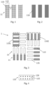
- FIG. 1 is a top view of a fifth structure 11, comprising three two-dimensional arrays of elements 110, wherein each element 110 is a nanowire.
- Each row of each array 115 comprises four elements 110, i.e., nanowires, and each column of each array 115 comprises twelve elements.
- the nanowires have a diameter of 20 nm, and a pitch between neighbouring nanowires is 50 nm.
- a distance between adjacent arrays 115 is, in this example, 1 ⁇ m.
- a third structure in accordance with embodiments of the present invention may have similar features as the fifth structure 11.
- each array 115 is observable as a rectangle, as shown in Fig. 2 , which is a schematic optical observation of the top of the arrays 115 in Fig. 1 .
- FIG. 3 is a top-view schematic representation of an optical overlay metrology area 1 of a semiconductor structure 9 in accordance with embodiments of the present invention.
- a fifth structure 11 comprises four times four two-dimensional arrays 115 of elements, similar to that shown in Fig. 1 and Fig. 2 , in a first layer 3.
- the overlay metrology area 1 further comprises a fourth structure 13, comprising four times four elements 135. Each element 135 of the fourth structure 13 has a sufficient size enabling accurate optical detection.
- the overlay metrology area 1 comprises a first group 1101 of identical, parallel, and equally spaced two-dimensional arrays 115 of the fifth structure, of which a longest side is perpendicular to a longest side of arrays 115 of the fifth structure of a second group 1102 of identical, parallel, and equally spaced two-dimensional arrays 115 of the fifth structure. It is an advantage of this configuration that an overlay error may be accurately determined in both of the perpendicular directions.
- the present invention is, however, not limited to this configuration and very different configurations may also be used in accordance with embodiments of the present invention.
- the optical overlay metrology area 1 further comprises one corresponding element 135 of the fourth structure 13 for each array 115 of the fifth structure 11, having dimensions identical to the rectangle formed by said arrays 115.
- the corresponding element 135 of the fourth structure 13 and array 115 of the fifth structure 11 are separated from each other by a distance that is at least 200 nm, preferably at least 4000 nm, so that features of the fourth structure 13, e.g., of the elements 135 (or possibly even subelements) thereof, may be easily distinguished from features of the fifth structure 11, e.g., of the arrays 115 or elements thereof.
- each corresponding element 135 of the fourth structure 13 and array 115 of the fifth structures 11 are oriented such that longest sides are parallel with respect to each other. Furthermore, the corresponding element 135 of the fourth structure 13 and array 115 of the fifth structure 11 are in line with each other, which may facilitate accurately determining a distance, e.g., a second distance, between features, e.g., centroids, of said corresponding structures. As many such corresponding elements 135 and arrays 115 are present in the optical overlay metrology area 1, a statistical error on said distance may be limited.
- Fig. 4 is a top-view schematic representation of a single element 135 of the fourth structure, and an array 125 of elements 120 a fifth structure located in the first layer in physical contact with, and pinning, the single element 135 of the fourth structure.
- the single element 135 of the fourth structure completely overlaps each of the periodically arranged identical elements 120 of the third structure.
- each element 120 of the third structure is a nanowire.
- the nanowire is orientated vertically.
- a total vertical extent measured perpendicularly to the top surface of the first layer is at least twice larger than the largest lateral extent, i.e., parallel to said top surface, of each element 120.
- each element 120 of the fifth structure has a top surface having an aspect ratio of 1.
- the length and width of each element 120 of the third structure is similar to that of a channel structure in a device area (not shown), typically at most 100 nm, so that the combination of the elements 120 of the third structure and the single element 135 of the fourth structure as accurately mimic the interaction between the first structure and the second structure of the real device.
- Example 2 Method for determining an overlay error between an electrode and a channel structure
- FIG. 5 is a schematic vertical cross-section of an intermediate structure 91 in the construction of the semiconductor structure.
- the intermediate structure 91 comprises an overlay metrology area 1 and a device area 2, that do not laterally overlap with each other.
- the device area 2 comprises an intermediate in the formation of a device that is, in this example, a vertical field effect transistor, comprising in a first layer 3, a first, channel, structure 21, and a gate structure 23 wrapped around the first structure 21.
- a top surface 211 of the first structure 21 is located above a top surface 31 of the first layer 3. As such, a portion of the first structure 21 protrudes into a second layer 4 on top of the first layer 3, thereby pinning the first structure 21 into the second layer 4.
- the device area 2 further comprises a first masking structure 62 of a mask layer 6 for forming a second structure 22, corresponding, in this example, to an electrode, in the second layer 4, which is formed of an electrically conducting material.
- Said mask layer 6 was patterned by the use of a lithographic mask.
- the overlay metrology area 1 comprises a fifth structure 11 and a third structure 12, both located in the first layer 3.
- the overlay metrology area 1 is for determining an overlay error between the first structure 21, e.g., the channel structure, and a second structure 22, e.g. an electrode, formed after patterning of the second layer 4.
- the overlay metrology area 1 comprises a second masking structure 61 of the mask layer 6 for forming a fourth structure 13 in the second layer 4.
- the second masking structure 61 overlaps with the third structure 12, so that the fourth structure 13 that is to be formed in the second layer 4 is in physical contact with the third structure 12.
- both the top surface 111 of the fifth structure 11 and the top surface 121 of the third structure 12 extend above the top surface 31 of the first layer 3, thereby pinning the second layer 4.
- This is particularly relevant for the third structure 12, as, in this way, an interaction between the third structure 12 and either the second layer 4, before the patterning, or the fourth structure 13, formed by the patterning, is similar to that between the first structure 21 and either the second layer 4, before the patterning, or the second structure, formed by the patterning, respectively.
- the second layer 4 is pinned also to the third structure 12.
- a first distance D1 is optically determined between features of the fifth structure 11 and features of the second masking structure 61.
- Said features may, for example, be edges of (arrays or elements of) the fifth structure 11 and the elements of the second masking structure 61, or (such as in this example) a centroid of the top surfaces of the fifth structure 11 and the second masking structure 61, although the invention is not limited thereto.
- the features that are used in the method may depend on the optical tool that is used for said optical determination, but is typically a centroid for ease of optical resolving.
- the masking layer 6 further comprises a third masking structure 63 in the overlay metrology area 1, for forming a sixth structure 81 in the second layer 4 unpinned to the first layer 3, and a fourth masking structure 64 in the device area 2, for forming a further unpinned structure 82 in the first layer 3 in the device area 2.
- a third distance D3 may optionally be determined between a feature of the third masking structure 63 and a feature of the fifth structure 11.
- the second layer 4 is etched, using the mask layer 6 as a mask, thereby forming the semiconductor structure 9 of Fig. 6 .
- stress and subsequent relaxation of the second layer 4 may occur, thereby possibly locally (or globally) inducing a lateral displacement of (parts of) the second layer 4 with respect to the first layer 3 during said etching.
- the overlay error determined in the optical overlay metrology area 1 may be assumed to be the same as in the device area 2.
- a second structure 22, i.e., electrode, is formed in physical contact with, and pinned by, the first structure 21, thereby forming the device (a further electrode, comprised in the device and located below and in physical contact with the first structure 21, is not shown in this example).
- a projection of a top surface of the first structure 21 on a bottom surface of the second structure 22 is, in this example, comprised in said bottom surface.
- a fourth structure 13 is formed in physical contact with, and pinned by, the third structure 12. In this example, a projection of a top surface 121 of the third structure 12 on a bottom surface 131 of the fourth structure 13 is comprised in the bottom surface 131 of said fourth structure 13.
- a second distance D2 is determined between the features of the fifth structure 11 (that are the same features of the fifth structure 11 as used for determining the first distance D1), and features of the fourth structure 13.
- Said features of the fourth structure 13 correspond to the features of the second masking structure 61 used for determining the first distance D1. This may be understood to mean, for example, that when a centroid of a top surface of the second masking structure 61 was used in determining the first distance D1, a centroid of a top surface of the fourth structure 13 is used in determining the second distance D2.
- a left edge of the second masking structure 61 was used in determining the first distance D1
- a left edge of the fourth structure 13 is used in determining the second distance D2.
- the second distance D2 is compared to the first distance D1 so as to determine a process induced overlay error between the first structure 21 and the second structure 22. Due to the similar interactions between the third 12 and fourth structure 13 described above in the overlay metrology area 1 and in the device area 2, the determined overlay error may be assumed to accurately represent an overlay error for the device formed in the device area 2. In this example, on comparison, D2 appears to be larger than D1, implying that the second structure 22 and the fourth structure 13 are slightly shifted to the right compared to the first masking structure 62 and the second masking structure 61.
- a sixth structure 81 in the optical overlay metrology area 1 and a further unpinned structure 82 in the device area 2 are formed. Overlay between the further unpinned structure 82 and the unpinned structure 24 is clearly not good.
- a fourth distance D4 may be measured between the feature of the fifth structure 11 and a feature of the sixth structure 81 corresponding to said feature of the third masking structure 63 used for (optionally) measuring the third distance D3. Similar as for the first distance D1 and second distance D2, an overlay error between the further unpinned structure 82 and an unpinned structure 24 in the first layer 3 may be determined based on the comparison between the third distance D3 and the fourth distance D4.
- distances are compared directly with respect to the same fifth structure 11, it is clear to the skilled person that, instead, more indirect measurements, e.g., by comparing with different reference structures, could be performed. For example, in a first mark, the first distance D1 and second distance D2 could be determined, and in a second mark, the third distance D3 and the fourth distance D4 could be determined, or the distances could be derived indirectly from different marks, via the use of references structures.
- the lithographic mask used for forming the masking layer may be shifted.
- This may be performed by shifting the mask pattern used for patterning of the masking layer 6. After processing of said intermediate to the semiconductor structure 91, i.e., by transferring the pattern from the masking layer 6 into the second layer 4, this may result in an accurate overlay of the second structure 22 and the first structure 21.
- this overlay error between the first structure 21 and the second structure 22 has to be compensated for at the same time as for the overlay error between the further unpinned structure 82 and the unpinned structure 24 in the first layer 3, in addition or alternatively to the shift of the lithographic mask, a redesign of said lithographic mask may be required.
- ⁇ ⁇ D3 - D4 to the right.
- the sixth structure 81 is unpinned, it may be expected that ⁇ ⁇ >> ⁇ .
- Example 3 Intermediate semiconductor structure for use in a method for determining an overlay error between an electrode and a channel structure
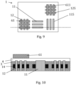
- Fig. 9 shows a top view of an overlay metrology area of an intermediate in the formation of a semiconductor structure, which may be used in a method in accordance with embodiments of the present invention.
- Fig. 10 which is a vertical cross-section of the intermediate shown in Fig. 9 , along the dashed line in Fig. 9 .
- the second layer 4 has a thickness below 60 nm, so that the fifth structure 11 and the third structure 12, both present in the first layer 3, are visible through the second layer 4.
- the fifth structure 11 comprises elements 115 that are (rectangular) sheets.
- a second masking structure 61 comprises rectangular elements 611.
- the third structure 12 comprises periodically arranged arrays 125 of nanosheets (not shown/unresolved).
- the fifth structure 11 and the third structure 12 both have an upper surface located above an upper surface of the first layer 3.
- each element of the second masking structure 61 overlaps three arrays of the third structure 12, and each array of the third structure 12 overlaps three elements of the second masking structure 61.
- the fifth structure 11 does not overlap with the third structure 12 not with the second masking structure 61.
- the overlay metrology area comprises a structure 14 made of a gate material in the first layer 3, wrapping around the elements of the fifth structure 11 and the (elements of the) third structure 12.
- Said gate material may improve mimicking of a device structure (not shown) that may also have a gate structure wrapping around its channel structure. A good mimicking may improve the accuracy of an overlay error.
- the second layer 4 may be etched so as to transfer the pattern of the second masking structure 61 into the second layer 4, thereby forming a fourth structure 13 in physical contact with the third structure 12.
- the pattern of the fourth structure is the same that of the second masking structure 61, similarly, also a vertical projection of a top surface of the third structure 12 on a bottom surface of the fourth structure 13 is only partially comprised in the fourth structure.
Landscapes
- Physics & Mathematics (AREA)
- General Physics & Mathematics (AREA)
- Engineering & Computer Science (AREA)
- Multimedia (AREA)
- Exposure And Positioning Against Photoresist Photosensitive Materials (AREA)
- Chemical & Material Sciences (AREA)
- Materials Engineering (AREA)
- Nanotechnology (AREA)
Abstract
Description
- The present invention relates to the field of overlay control in the manufacturing of semiconductor devices. In particular, the present invention relates to a device comprising an overlay metrology area for evaluating an overlay error, and a method for determining an overlay error.
- Controlling of an overlay between semiconductor device structures, e.g., elements of a semiconductor device, in different layers, by optically detecting a distance between periodic structures in the different layers, located in an overlay metrology area that is separated from the area wherein the device structures are formed, is well-established in the semiconductor industry. Overlay control facilitates good accuracy and reproducibility of stacking of layers in semiconductor processes. Also techniques different from optical techniques may be used for overlay control, including, notably, electron microscopy. However, optical techniques have the advantage of speed, and may be easily performed in line, for example during semiconductor device production. Furthermore, as, for example, described in SILVER, Richard M., et al. High-resolution optical overlay metrology. In: Metrology, Inspection, and Process Control for Microlithography XVIII. International Society for Optics and Photonics, 2004. p. 78-95, overlay control by optical techniques is not limited by the Rayleigh limit, corresponding to the wavelength of light used in the optical technique, which is typically hundreds of nanometers. Indeed, in the state of the art, optical overlay control may be performed at a resolution of below 10 nm.
- As an example,
US9093458B2 - As dimensions of devices become smaller and smaller, requirements on overlay control become ever more stringent. Thus, there is still a need in the art for devices and methods that facilitate good overlay control.
- It is an object of the present invention to provide good apparatus and methods for evaluating an overlay error.
- The above objective is accomplished by a method and device according to embodiments of the present invention.
- It is an advantage of embodiments of the present invention that a first structure and a second structure, located in a device area, are accurately represented by a combination of a third structure and a fourth structure, located in an optical overlay metrology area, used for evaluating an overlay error. It is a further advantage of embodiments of the present invention that said accurate representation may result in an overlay error measured in the optical overlay metrology area that is representative of an overlay error between structures in the device area.
- In a first aspect, the present invention relates to a semiconductor structure comprising a first layer and a second layer on top thereof and in physical contact therewith. The semiconductor structure comprises a device area at least comprising a first structure in the first layer having a top surface above a top surface of the first layer, and a second structure in the second layer in physical contact with the first structure, such that the first structure is pinned in the second structure. The semiconductor structure further comprises an optical overlay metrology area for optically evaluating an overlay error between the second structure and the first structure. Said optical overlay metrology area comprises: a third structure in the first layer, formed of a material of which the first structure is formed, and having a top surface above the top surface of the first layer, a fourth structure in the second layer, formed of a material of which the second structure is formed, in physical contact with the third structure, such that the combination of the third and fourth structures mimics the combination of the first and second structures, and a fifth structure in the first layer for use as a reference structure.
- The inventors have unexpectedly observed that an overlay error determined using an optical overlay metrology area of the state of the art, for which there is no third structure as in accordance with the present invention, and thus wherein the combination of the third and fourth structures mimicking the combination of the first and second structures does not appear, may not correspond to an actual overlay error between the first structure and the second structure. In other words, the determined overlay error unexpectedly appeared to be inaccurate. The inventors have found that relaxation processes in a second layer as a result of the etching of said second layer may result in slight displacement of the second layer, with respect to the first layer. Said displacement may be different in the device area than in the overlay metrology area. The inventors have found that this difference appeared to be due to differences in interaction between the first and second layer, or correspondingly the first structure and the second structure, in the device area and between the first and second layer in the overlay metrology area. The overlay error may more accurately represent the actual overlay error between the first and second structure in the device area, when an interaction between the first layer and the second layer is mimicked in the overlay metrology area. In an attempt to accurately mimic said interaction, the present invention comprises the third structure combined with the fourth structure, for mimicking the combination of the first and second structure.
- In embodiments, said mimicking comprises that the third structure is pinned in the fourth structure, preferably the same way the first structure is pinned in the second structure. It is an advantage of embodiments of the present invention that the pinning of the first structure in the second structure is mimicked by the third structure being pinned in the fourth structure.
- In embodiments, the first structure is a channel formed of a channel material. In these embodiments, the third structure may also be formed of said channel material. Furthermore, the fifth structures may be formed of said channel material. In embodiments, the channel material comprises an n-doped semiconductor material or a p-doped semiconductor material, wherein the semiconductor material is preferably silicon.
- In embodiments, the second structure is an electrode formed of an electrically conductive material, and the fourth structure is formed of said electrically conductive material. In embodiments, the second structure and the fourth structure are formed of a metal, preferably tungsten. The inaccuracy in the determined overlay error may be particularly pronounced when the second structure is formed of a relatively high tensile strength material, such as tungsten.
- In preferred embodiments, the first structure is the channel, and the second structure is the electrode. In embodiments, the device area comprises a gate structure, formed of a gate material, in the first layer wrapping the channel. In these embodiments, preferably, the optical overlay metrology area comprises a structure formed of said gate material in the first layer wrapping the third structure. In these embodiments, preferably, the optical overlay metrology area comprises a structure formed of said gate material in the first layer wrapping the fifth structure. Said gate material may improve mimicking of the device structure, possibly further improving the accuracy of the determination of the overlay error.
- In embodiments, the device area comprises a semiconductor device, such as a field effect transistor, e.g., a vertical field effect transistor. In embodiments, the first structure and the second structure are part of the semiconductor device, preferably of the vertical field effect transistor. The vertical field effect transistor may comprise a further electrode, wherein the vertical field effect transistor is located above and in physical contact with the further electrode. The invention is, however, not limited to vertical field effect transistors, and instead, the semiconductor device may be a complementary field effect transistor.
- In embodiments, the third structure comprises an, i.e., at least one, array of elements. In embodiments, the array is a two-dimensional array, e.g., comprises rows and columns of elements. In embodiments, each row, oriented along a first direction parallel to the top surface of the first layer, comprises at least two elements, and each column, oriented along a second direction parallel to the top surface of the first layer and perpendicular to the first direction, comprises at least two, preferably at least five, elements. In embodiments, each array of the third structure comprises a plurality of elements, e.g., from 2 to 200 elements. In embodiments, a first pitch between a first element and a last element in a row of the array of elements of the third structure is from 200 nm to 2000 nm, and a second pitch between a first element and a last element in a column of the array of elements of the third structure is from 500 nm to 20 µm. In embodiments, a ratio of the second pitch to the first pitch is at least two, preferably at least five. In embodiments, a pitch between adjacent elements of the array is from 20 nm to 200 nm. The array of elements of the third structure is preferably a periodic array, preferably defining a rectangle. Said periodicity may, for example, avoid asymmetry effects from any processes. Said periodicity may at least mean that the pitch between each pair of adjacent elements within the periodic array is substantially the same. Said periodicity may at least mean that a width, parallel to the top surface of the first layer, of each element in the periodic array is substantially the same. Said periodicity may at least mean that the elements of the periodic array of the third structure are substantially identical.
- In preferred embodiments, the third structure comprises at least two, preferably at least five arrays of elements. In embodiments, neighbouring arrays are separated from each other by a distance of from 200 nm to 4000 nm, preferably from 500 to 1500 nm, more preferably from 800 to 1200 nm. The arrays may form a periodic structure, e.g., the third structure may be a periodic third structure. In embodiments, the arrays are symmetrically distributed throughout the third structure, e.g., the third structure may be substantially mirror symmetric, or centrosymmetric. In particular embodiments, a distance between each pair of adjacent arrays of the third structure is substantially the same.
- In embodiments, the fourth structure comprises a, i.e., at least one, preferably at least two, more preferably at least five, elements. In embodiments, each element of the fourth structure has a width, in a direction parallel to the top surface of the first layer, and a length, in a direction parallel to the top surface of the first layer and perpendicular to the width, that are at least 100 nm, preferably at least 200 nm, more preferably at least 500 nm. In embodiments, a ratio of the length to the width is at least two, preferably at least five. In embodiments, each element of the fourth structure has a width and a length which is each at least 5 times larger, preferably at least 10 times larger, than respectively a width and a length of an element of the third structure. Herein, the width and length are perpendicular to each other, and parallel to a top surface of the first layer. Preferably, each element of the fourth structure has substantially identical dimensions. In preferred embodiments, a longest side of adjacent fourth structures is orientated parallel with respect to each other. In embodiments, the fourth structure is in physical contact with a plurality of elements of the third structure, e.g., with each element of an array of the third structure. In embodiments wherein the third structure comprises an array of elements, preferably, the fourth structure is in physical contact with each element of the third structure. While dimensions of the elements of the third structure may be small so as to mimic interactions between the first and second structure so as to improve the overlay error, at the same time, the size of elements of the fourth structure is preferably sufficiently large so as to facilitate optical detection, and for ease of formation. As each element of the fourth structure may, independently from other elements of the fourth structure, be used to determine an overlay error, a higher number of elements in the fourth structures may result in a lower statistical error on a determined overlay error. In preferred embodiments, each element of the fourth structure is a solid piece of material, preferably a cuboid or a rectangular cuboid bar. The invention is, however, not limited thereto, and in some embodiments, each element of the fourth structure comprises subelements, e.g., an array of subelements. For instance, a long bar could be segmented to a plurality of short bars. In particular embodiments, each element of the fourth structure comprises one subelement for each element of the third structure overlapped by the element of the fourth structure.
- In embodiments, the elements of the fourth structure are symmetrically distributed throughout the fourth structure, e.g., the fourth structure may be substantially mirror symmetric, or centrosymmetric. In embodiments, a distance between each pair of adjacent elements of the fourth structure is substantially the same.
- In embodiments, the fifth structure is not limited to a particular form, as it mainly functions as a reference structure. In embodiments, the fifth structure comprises at least one array of elements. In embodiments, the array is a two-dimensional array, i.e., comprises rows and columns of elements. In embodiments, each row, oriented along a first direction parallel to the top surface of the first layer, comprises at least one, preferably at least two elements, and each column, oriented along a second direction parallel to the top surface of the first layer and perpendicular to the first direction, comprises at least one, preferably at least two, preferably at least five, elements. In particular embodiments, each array of the fifth structure comprises a single element. However, typically, each array of the fifth structure comprises a plurality of elements, e.g., from 2 to 200 elements. In embodiments, a first pitch between a first element and a last element in a row of the array of the fifth structure is from 200 nm to 2000 nm, and a second pitch between a first element and a last element in a column of the array of the fifth structure is from 500 nm to 20 µm. In embodiments, a ratio of the second pitch to the first pitch is at least two, preferably at least five. In embodiments, said first and second pitch are substantially the same as a width and a length of elements of the fourth structure. In embodiments, a pitch between adjacent elements of the array of the fifth structure is from 20 nm to 200 nm. The array is preferably a periodic array, preferably defining a rectangle. It is an advantage of these embodiments that asymmetry effects arising from any processes may be avoided. It is a further advantage of these embodiments that said periodicity may result in a homogeneous, optically observable rectangle. As such, said periodic array may comprise features that may be optically well-defined and may result in a resolution for determining features of the fifth structure, well below the Rayleigh limit, e.g., below 10 nm. Said periodicity may at least mean that the pitch between adjacent elements is substantially the same. Said periodicity may at least mean that a width, parallel to the top surface of the first layer, of each element in the periodic array is substantially the same. Said periodicity may at least mean that the elements of the periodic array are substantially identical.
- In preferred embodiments, the fifth structure comprises at least two, preferably at least five, arrays. In embodiments, neighbouring arrays are separated from each other by a distance of from 200 nm to 4000 nm, preferably from 500 to 1500 nm, more preferably from 800 to 1200 nm. In embodiments, a distance between each pair of arrays is substantially the same. In embodiments, longest edges of neighbouring arrays are oriented substantially parallel with respect to each other. It is an advantage of embodiments that features of a first array of the fifth structure may be distinguished from features of a second, neighbouring, array of the fifth structure. As each array may, independently from other arrays, be used to determine an overlay error, a higher number of arrays present in the optical overlay metrology area may result in a lower statistical error on a determined overlay error.
- In embodiments, the fifth structure, i.e., elements of the fifth structure, has a top surface above a top surface of the first layer, but this is not required by the present invention. However, the fifth structure having the top surface above the top surface of the first layer, similar as the third structure having the top surface above the top surface of the first layer, may be a result of the same processing that is applied to the third structure as to the fifth structure. In embodiments, for each element of the third structure, the fifth structure comprises a corresponding element in an array of elements of the fifth structure. Thereby, a distance between features of one element of the third structure and features of one array of the fifth structure may be determined. The invention is, however, not limited thereto.
- In embodiments, the arrays of elements of the fifth structure are symmetrically distributed throughout the fifth structure, e.g., the fifth structure may be substantially mirror symmetric, or centrosymmetric. In embodiments, a distance between each pair of adjacent elements of the fifth structure is substantially the same.
- In embodiments, arrays and elements of the fifth structure are sufficiently separated from arrays and elements of the fourth structure, such that features of the fifth structure and features of the fourth structure may be easily distinguished from each other. In embodiments, a gap between elements of the fifth structure and elements of the fourth structure is at least 100 nm, preferably at least 200 nm, more preferably at least 400 nm.
- In embodiments, the first structure has a top surface having an aspect ratio of from 1 to 5, preferably from 1 to 2. In embodiments, each element of the third structure, and possibly each element of the fifth structure, preferably has an aspect ratio of from 1 to 5, more from preferably 1 to 2. In embodiments, the first structure has a total vertical extent measured perpendicularly to the top surface of the first layer which is at least twice larger than the largest lateral extent of the first structure. In embodiments, the elements of the third structure, and possibly the elements of the fifth structure preferably, have a total vertical extent measured perpendicularly to the top surface of the first layer which is at least twice larger than the largest lateral extent of the third and fifth structure, respectively. In embodiments, the first structure has a width, parallel to a top surface of the first layer, that is at most 100 nm, preferably at most 50 nm. In these embodiments, preferably, the elements of the third structure, and possibly the elements of the fifth structure, have a width, parallel to a top surface of the first layer, that is at most 100 nm, preferably at most 50 nm. In preferred embodiments, an area of a top surface of each element of the third structure, measured in a plane parallel to a top surface of the first layer, is within 100%, preferably within 20%, of an area of a top surface of the first structure, measured in a plane parallel to the top surface of the first layer. In some embodiments, an area of a top surface of each element of the fifth structure, measured in a plane parallel to a top surface of the first layer, is within 100%, preferably within 20%, of an area of a top surface of the first structure, measured in a plane parallel to the top surface of the first layer. In embodiments, the first structure is a nanowire. In these embodiments, preferably, the elements of the third structure are nanowires. In embodiments wherein the first structure is a nanowire, the elements of the fifth structure are nanowires. In different embodiments, the first structure is a nanosheet. In these embodiments, preferably, the elements of the third structure are nanosheets. In embodiments wherein the first structure is a nanosheet, the elements of the fifth structure may be nanosheets.
- In still different embodiments, each array of the fifth structure is a solid piece of material, preferably a cuboid or a rectangular cuboid bar, which corresponds to each element of the fifth structure being a solid piece of material, preferably a cuboid or a rectangular cuboid bar. In these embodiments, each element of the fifth structure has a width, in a direction parallel to the top surface of the first layer, and a length, in a direction parallel to the top surface of the first layer and perpendicular to the width, that are at least 100 nm, preferably at least 200 nm, more preferably at least 500 nm.
- In embodiments, the semiconductor structure comprises, in the optical overlay metrology area, in the second layer, a sixth structure for use as a further reference, unpinned by any structure in the first layer. Said sixth structure may be formed of the same material as the second structure. The sixth structure may be used to determine an overlay error for unpinned structures in the device area, when present, so that also an appropriate correction may be applied for such unpinned structures.
- Any features of any embodiment of the first aspect may be independently as correspondingly described for any embodiment of the second aspect of the present invention.
- In a second aspect, the present invention relates to a method for determining an overlay error between a first structure and a second structure in a semiconductor structure. The method comprises a step of: i) obtaining an intermediate structure to the formation of the semiconductor structure, comprising a first layer, a second layer on top of the first layer, and a masking layer over the second layer. Said intermediate structure comprises: 1) a device area comprising: a) the first structure in the first layer, having a top surface above a top surface of the first layer, b) the second layer, formed of a material of the second structure, in physical contact with the first structure, such that the first structure is pinned in the second layer, and c) a first masking structure in the masking layer, overlapping with the first structure, and 2) an optical overlay metrology area comprising: a) a third structure in the first layer, having a top surface above the top surface of the first layer, b) the second layer, typically formed of a material of which the second structure is formed, in physical contact with the third structure, such that the third structure is pinned in the second layer, c) a second masking structure in the masking layer, overlapping with the third structure, and d) a fifth structure in the first layer. The method further comprises a step of: ii) optically detecting a first distance between a feature of the second masking structure and a feature of the fifth structure. The method further comprises a step of: iii) etching the second layer, by using the first and second masking structure as a mask, so as to form the second structure, in physical contact with the first structure, and a fourth structure, in physical contact with the third structure. The method further comprises a step of: iv) optically detecting a second distance between a feature of the fourth structure, corresponding to said feature of the second masking structure, and said feature of the fifth structure. The method further comprises a step of: v) comparing the first distance with the second distance.
- It is an advantage of embodiments of the present invention that an overlay error determined between the first structure and the second structure is based on a third and fourth structure in the overlay metrology area that, in combination, accurately mimic the combination of the first and second structure in the device area. As such, the present invention may provide information on the shift between the location of the first masking structure, that is for forming the second structure, and the second structure subsequently formed therewith. Said overlay error may be used to correct the location at which a further masking layer is formed in a further semiconductor structure, such that, in subsequent runs for forming the further semiconductor structures, corresponding further second structures are formed at the correct location over, i.e., correctly overlaying, the corresponding first structures in said further semiconductor structure. Said correction to the location of the mask may be applied locally, e.g., a further masking layer for forming the further second structure in the further semiconductor structure may be relocated compared to the corresponding location of the masking for forming the semiconductor structure, in accordance with the overlay error that is determined. This may, however, require redesign of a mask pattern used for forming the masking layer, e.g., by redesigning the lithographic mask used for forming the masking layer (e.g., when the masking layer is formed of a photoresist material so that the pattern of the mask pattern may be transferred into the masking layer by (E)UV radiation), which may be time-consuming and expensive. Typically, therefore, the correction is applied by shifting the complete mask pattern used for forming the masking layer, e.g., by moving the lithographic mask as a whole, such that further, corresponding masking layers in further semiconducting structures result in good overlap between the corresponding further first structure and the corresponding further second structure. As such, the overlay error measurement of the present invention may be used for a correction to the transfer of the pattern from the mask pattern to the masking layer for better alignment.
- As the overlay error depends on several processing parameters, and may furthermore depend on location on a wafer in which the semiconductor structure is formed, embodiments of the method of the present invention may need to be applied for each process, possibly at multiple locations scattered over the wafer.
- In embodiments, the masking layer may be formed of a photoresist. In embodiments, a mask pattern is used to form a pattern, comprising at least the first and second masking structure in the masking layer. For example, a pattern in the mask pattern may be transferred into the masking layer by illumination, preferably by UV or EUV irradiation. Either a positive or a negative photoresist may be used.
- Lateral dimensions of the first and second structure, and possibly third structure, in the masking layer typically correspond to lateral dimensions of the second and fourth, and possibly sixth, structures formed therewith, after the etching, respectively.
- In embodiments, obtaining the intermediate structure comprises: obtaining the first layer comprising the third structure, having a top surface coplanar with the top surface of the first layer; epitaxially growing material, of which the third structure is formed, on the top surface of the third structure, thereby bringing its top surface above the top surface of the first layer; and depositing the second layer on the first layer.
- In embodiments, the second layer of the intermediate structure in the construction of the semiconductor structure has a thickness of at most 60 nm, preferably at most 30 nm. This is particularly relevant in embodiments wherein the fifth structure is comprised in the first layer and is formed of a channel material. In those embodiments, the first distance may be determined based on optical detection of a feature of the fifth structure through the second layer. It is therefore preferred that absorption of light by the second layer is limited, which may be the case when the second layer is thin.
- In embodiments, said optically detecting may be performed by optically detecting the semiconductor structure from above. Illumination may be performed from above, e.g., in backscattering configuration, but this is not required. Although this may, in principal, be performed with any optical detector for detecting sufficiently small features in the semiconductor structure, commercial optical detectors are available, such as a commercial optical inspection machine (KLA-700) for overlay measurement. The characteristics typically used to optimize detection (signal to noise ratio) are wavelength and illumination modes. In embodiments, the wavelength of the light used for said detection may be from 50nm to 2000 nm, preferably from 150 to 1000 nm, more preferred from 350 to 1000 nm.
- In embodiments, optically detecting the first and second distances comprises optically detecting lateral distances, i.e., distances in a direction in a plane parallel to a top surface of the first layer. In embodiments, the first distance is determined between features of the second masking structure and features of the fifth structure. In embodiments, said features may be a centroid or an edge of individual elements or arrays, although the invention is not limited to any type of features. As an example, a (masking or other) structure may comprise five bar patterns with a fixed spacing in between. A measurement tool may first be programmed to detect the edge of each bar of the structure. The center line of each bar may be determined by their edge positions. The center of the gravity of the structure can then be obtained from the center lines.
- Typically, the used features of the second masking structure correspond to the used features of the fifth structure, e.g. a distance is measured between the centroid of the second masking structure and the centroid of the fifth structure. The second distance is determined based on corresponding features in the fourth structure and the second masking structure. This means that, when, in detecting the first distance, for example, a centroid of the second masking structure was used, for measuring the second distance, correspondingly, a centroid of the fourth structure is used.
- In embodiments, etching the second layer comprises performing an etching technique that selectively etches the second layer with respect to the masking layer. In embodiments, said etching comprises performing a liquid etch, e.g., using a hydroxide or H2O2, although the etching technique is not limited thereto. In alternative embodiments, for instance, dry etching, such as reactive ion etching (RIE), may be used. RIE can produce very anisotropic etch profiles, in contrast to the typically isotropic profiles of wet etching, which is advantageous for producing structures with very fine dimension.
- In particular embodiments, obtaining the intermediate structure comprises obtaining, in the masking layer, a third masking structure, not overlapping with any structure for pinning in the first layer, further comprising a step of optically detecting a third distance between a feature of the third masking structure and a feature of the fifth structure or a feature of the second masking structure. Said etching the second layer then also comprises using the third masking structure as a mask so as to form a sixth structure in the second layer, unpinned by any structure in the first layer. The method further comprises optically detecting a fourth distance between the fourth structure or the fifth structure, and the sixth structure. The third distance is then compared to the fourth distance so as to determine a lateral shift of the sixth structure in the second layer, unpinned by the underlaying first layer. This may provide information on lateral shifts of unpinned structure in the device area with respect to the mask structure with which they are formed. In these embodiments, the method may further comprise determining an overlay error for unpinned structures in the first and second layers based on the comparison between the third distance and the fourth distance. Furthermore, in embodiments, the method may comprise determining the lateral shift attributed to the stress release in the second layer from the comparison of the third distance and the fourth distance and the comparison of the first distance and the second distance. Similar as for the overlay error between the first and second structure, the overlay error for unpinned structure may be compensated for. If both types of overlay error are to be compensated for at the same time, a redesign of the mask pattern may be required.
- Typically, the first distance and the second distance are determined in a same, lateral direction. By comparing the first distance with the second distance, it may be derived how much the fourth structure is shifted with respect to the second masking structure used for forming the fourth structure. In embodiments, the method further comprises determining an overlay error for pinned structures in the first and second layers based on the comparison between the first distance and the second distance. This may, for example, be determined by calculating the difference between the first distance and the second distance, e.g., by subtracting the second distance from the first distance. This result may correspond with a lateral shift of the fourth structure with respect to the second masking structure, and is typically the same as for a lateral shift of the second structure with respect to the first masking structure. In embodiments, the method further comprises applying the overlay error for pinned structures to reposition a mask pattern used for forming the masking layer. As mentioned above, preferably, the complete mask pattern is repositioned, e.g., shifted by an amount equal to the difference between the first distance and the second distance, in a same direction as wherein the first distance and the second distance were determined. The above described method may be repeated for different, for instance perpendicular, lateral directions as defined by the array of structures.
- Any features of any embodiment of the second aspect may be independently as correspondingly described for any embodiment of the first aspect of the present invention.
- Particular and preferred aspects of the invention are set out in the accompanying independent and dependent claims. Features from the dependent claims may be combined with features of the independent claims and with features of other dependent claims as appropriate and not merely as explicitly set out in the claims.
- The above and other characteristics, features and advantages of the present invention will become apparent from the following detailed description, taken in conjunction with the accompanying drawings, which illustrate, by way of example, the principles of the invention. This description is given for the sake of example only, without limiting the scope of the invention. The reference figures quoted below refer to the attached drawings.
-
-
Fig. 1 is a top-view schematic representation of a fifth structure in accordance with embodiments of the present invention. -
Fig. 2 is a top-view schematic representation of a fifth structure in accordance with embodiments of the present invention, detected with optical tools having a resolution larger than the width of elements of the fifth structure. -
Fig. 3 is a top-view schematic representation of an overlay metrology area of a semiconductor structure in accordance with embodiments of the present invention. -
Fig. 4 is a top-view schematic representation of a single element of the fourth structure, overlaying an array of elements of a third structure, in accordance with embodiments of the present invention. -
Fig. 5 is a schematic vertical cross-section of an intermediate in the construction of a semiconductor structure for use in a method in accordance with embodiments of the present invention. -
Fig. 6 is a schematic vertical cross-section of a semiconductor structure in accordance with embodiments of the present invention. -
Fig. 7 is a schematic vertical cross-section of an intermediate in the construction of a semiconductor structure to which overlay error correction has been applied. -
Fig. 8 is a schematic vertical cross-section of a semiconductor structure to which overlay error correction has been applied. -
Fig. 9 is a schematic top view of an overlay metrology area of an intermediate in the formation of a semiconductor structure, which may be used in a method in accordance with embodiments of the present invention. -
Fig. 10 is a schematic vertical cross-section of an overlay metrology area of an intermediate in the formation of a semiconductor structure, which may be used in a method in accordance with embodiments of the present invention. - In the different figures, the same reference signs refer to the same or analogous elements.
- The present invention will be described with respect to particular embodiments and with reference to certain drawings but the invention is not limited thereto but only by the claims. The drawings described are only schematic and are non-limiting. In the drawings, the size of some of the elements may be exaggerated and not drawn on scale for illustrative purposes. The dimensions and the relative dimensions do not correspond to actual reductions to practice of the invention.
- Furthermore, the terms first, second, third and the like in the description and in the claims, are used for distinguishing between similar elements and not necessarily for describing a sequence, either temporally, spatially, in ranking or in any other manner. It is to be understood that the terms so used are interchangeable under appropriate circumstances and that the embodiments of the invention described herein are capable of operation in other sequences than described or illustrated herein.
- Moreover, the terms top, bottom, over, under and the like in the description and the claims are used for descriptive purposes and not necessarily for describing relative positions. It is to be understood that the terms so used are interchangeable under appropriate circumstances and that the embodiments of the invention described herein are capable of operation in other orientations than described or illustrated herein.
- It is to be noticed that the term "comprising", used in the claims, should not be interpreted as being restricted to the means listed thereafter; it does not exclude other elements or steps. It is thus to be interpreted as specifying the presence of the stated features, integers, steps or components as referred to, but does not preclude the presence or addition of one or more other features, integers, steps or components, or groups thereof. The term "comprising" therefore covers the situation where only the stated features are present and the situation where these features and one or more other features are present. The word "comprising" according to the invention therefore also includes as one embodiment that no further components are present. Thus, the scope of the expression "a device comprising means A and B" should not be interpreted as being limited to devices consisting only of components A and B. It means that with respect to the present invention, the only relevant components of the device are A and B.
- Similarly, it is to be noticed that the term "pinned", also used in the claims, means that features have direct connections by protruding parts and recesses fitting into one another. The pinning is a more intimate connection than a simple physical contact of two adjacent structures or layers. Recesses in a particular structure do not have to be provided as such, but can be formed for instance by depositing the particular structure over an earlier formed structure having pinning features sticking out.
- Reference throughout this specification to "one embodiment" or "an embodiment" means that a particular feature, structure or characteristic described in connection with the embodiment is included in at least one embodiment of the present invention. Thus, appearances of the phrases "in one embodiment" or "in an embodiment" in various places throughout this specification are not necessarily all referring to the same embodiment, but may. Furthermore, the particular features, structures or characteristics may be combined in any suitable manner, as would be apparent to one of ordinary skill in the art from this disclosure, in one or more embodiments.
- Similarly it should be appreciated that in the description of exemplary embodiments of the invention, various features of the invention are sometimes grouped together in a single embodiment, figure, or description thereof for the purpose of streamlining the disclosure and aiding in the understanding of one or more of the various inventive aspects. This method of disclosure, however, is not to be interpreted as reflecting an intention that the claimed invention requires more features than are expressly recited in each claim. Rather, as the following claims reflect, inventive aspects lie in less than all features of a single foregoing disclosed embodiment. Thus, the claims following the detailed description are hereby expressly incorporated into this detailed description, with each claim standing on its own as a separate embodiment of this invention.
- Furthermore, while some embodiments described herein include some but not other features included in other embodiments, combinations of features of different embodiments are meant to be within the scope of the invention, and form different embodiments, as would be understood by those in the art. For example, in the following claims, any of the claimed embodiments can be used in any combination.
- In the description provided herein, numerous specific details are set forth. However, it is understood that embodiments of the invention may be practiced without these specific details. In other instances, well-known methods, structures and techniques have not been shown in detail in order not to obscure an understanding of this description.
- The invention will now be described by a detailed description of several embodiments of the invention. It is clear that other embodiments of the invention can be configured according to the knowledge of persons skilled in the art without departing from the true spirit or technical teaching of the invention, the invention being limited only by the terms of the appended claims.
- When an overlay control method in accordance with the prior art was performed, the inventors observed inaccuracies in the overlay error between the overlay error measured in an optical overlay metrology area and measured for a real device. The overlay control method was performed as follows. A first reference structure was formed in an optical overlay metrology area in a first layer. Furthermore, a first, channel, structure was formed a device area in said first layer. A second layer formed of tungsten was formed on the first layer, in physical contact with the fifth structure and the channel structure. A masking layer was formed over the second layer, comprising a first masking structure overlapping the channel structure in the device area, and comprising a second masking structure in the optical overlay metrology area, such that there is no overlap between the second masking structure and the third structure (i.e., in accordance with the prior art). A first lateral distance was optically detected between features of the second masking structure and features of the first reference structure.
- Subsequently, the second layer was patterned using an etching technique, so as to transfer the pattern of the first and second masking structures into the second layer. As a result, an electrode was formed on the channel structure, thereby forming a device in the device area comprising the electrode and the channel structure. Furthermore, a second reference structure was formed in the second layer and in physical contact with the first layer. Subsequently, a second distance was optically detected between features of the second reference structure, corresponding to the features of the second masking structure, and the features of the first reference structure. The first and second distance were compared so as to determine an overlay error. From the optical measurements in the overlay metrology area, it was concluded that the overlay error was very large. However, from SEM measurements performed on the device the actual overlay error appeared to be very small for the device. This is in stark contrast with the overlay error derived from the overlay metrology area, indicating that overlay control in accordance with the state of the art may not be accurate.
- In a first aspect, the present invention relates to a semiconductor structure comprising a first layer and a second layer on top thereof and in physical contact therewith. The semiconductor structure comprises a device area at least comprising a first structure in the first layer having a top surface above a top surface of the first layer, and a second structure in the second layer in physical contact with the first structure, such that the first structure is pinned in the second structure. The semiconductor structure further comprises an optical overlay metrology area for optically evaluating an overlay error between the second structure and the first structure. Said optical overlay metrology area comprises: a third structure in the first layer, formed of a material of which the first structure is formed, and having a top surface above the top surface of the first layer, a fourth structure in the second layer, formed of a material of which the second structure is formed, in physical contact with the third structure, such that the combination of the third and fourth structures mimics the combination of the first and second structures, and a fifth structure in the first layer for use as a reference structure.
- In a second aspect, the present invention relates to a method for determining an overlay error between a first structure and a second structure in a semiconductor structure. The method comprises a step of: i) obtaining an intermediate structure to the formation of the semiconductor structure, comprising a first layer, a second layer on top of the first layer, and a masking layer over the second layer. Said intermediate structure comprises: 1) a device area comprising: a) the first structure in the first layer, having a top surface above a top surface of the first layer, b) the second layer, formed of a material of the second structure, in physical contact with the first structure, such that the first structure is pinned in the second layer, and c) a first masking structure in the masking layer, overlapping with the first structure, and 2) an optical overlay metrology area comprising: a) a third structure in the first layer, having a top surface above the top surface of the first layer, b) the second layer, typically formed of a material of which the second structure is formed, in physical contact with the third structure, such that the third structure is pinned in the second layer, c) a second masking structure in the masking layer, overlapping with the third structure, and d) a fifth structure in the first layer. The method further comprises a step of: ii) optically detecting a first distance between a feature of the second masking structure and a feature of the fifth structure. The method further comprises a step of: iii) etching the second layer, by using the first and second masking structure as a mask, so as to form the second structure, in physical contact with the first structure, and a fourth structure, in physical contact with the third structure. The method further comprises a step of: iv) optically detecting a second distance between a feature of the fourth structure, corresponding to said feature of the second masking structure, and said feature of the fifth structure. The method further comprises a step of: v) comparing the first distance with the second distance.
- Reference is made to
Fig. 1 , which is a top view of afifth structure 11, comprising three two-dimensional arrays ofelements 110, wherein eachelement 110 is a nanowire. Each row of eacharray 115 comprises fourelements 110, i.e., nanowires, and each column of eacharray 115 comprises twelve elements. In this example, the nanowires have a diameter of 20 nm, and a pitch between neighbouring nanowires is 50 nm. A distance betweenadjacent arrays 115 is, in this example, 1 µm. When using optical tools to observe the three two-dimensional arrays 115 of thefifth structure 11, for example using light having a wavelength of 400 nm,individual elements 110 may not be resolvable, but neighbouringarrays 115 may be distinguished from each other. A third structure in accordance with embodiments of the present invention may have similar features as thefifth structure 11. As such, in this example, eacharray 115 is observable as a rectangle, as shown inFig. 2 , which is a schematic optical observation of the top of thearrays 115 inFig. 1 . - Reference is made to
Fig. 3 , which is a top-view schematic representation of an opticaloverlay metrology area 1 of asemiconductor structure 9 in accordance with embodiments of the present invention. Afifth structure 11 comprises four times four two-dimensional arrays 115 of elements, similar to that shown inFig. 1 and Fig. 2 , in afirst layer 3. Theoverlay metrology area 1 further comprises afourth structure 13, comprising four times fourelements 135. Eachelement 135 of thefourth structure 13 has a sufficient size enabling accurate optical detection. - In this example, the
overlay metrology area 1 comprises afirst group 1101 of identical, parallel, and equally spaced two-dimensional arrays 115 of the fifth structure, of which a longest side is perpendicular to a longest side ofarrays 115 of the fifth structure of asecond group 1102 of identical, parallel, and equally spaced two-dimensional arrays 115 of the fifth structure. It is an advantage of this configuration that an overlay error may be accurately determined in both of the perpendicular directions. The present invention is, however, not limited to this configuration and very different configurations may also be used in accordance with embodiments of the present invention. - In this example, the optical
overlay metrology area 1 further comprises onecorresponding element 135 of thefourth structure 13 for eacharray 115 of thefifth structure 11, having dimensions identical to the rectangle formed by saidarrays 115. In this example, thecorresponding element 135 of thefourth structure 13 andarray 115 of thefifth structure 11 are separated from each other by a distance that is at least 200 nm, preferably at least 4000 nm, so that features of thefourth structure 13, e.g., of the elements 135 (or possibly even subelements) thereof, may be easily distinguished from features of thefifth structure 11, e.g., of thearrays 115 or elements thereof. In this example, eachcorresponding element 135 of thefourth structure 13 andarray 115 of thefifth structures 11 are oriented such that longest sides are parallel with respect to each other. Furthermore, thecorresponding element 135 of thefourth structure 13 andarray 115 of thefifth structure 11 are in line with each other, which may facilitate accurately determining a distance, e.g., a second distance, between features, e.g., centroids, of said corresponding structures. As many suchcorresponding elements 135 andarrays 115 are present in the opticaloverlay metrology area 1, a statistical error on said distance may be limited. - Reference is made to
Fig. 4 , which is a top-view schematic representation of asingle element 135 of the fourth structure, and anarray 125 of elements 120 a fifth structure located in the first layer in physical contact with, and pinning, thesingle element 135 of the fourth structure. In this example, thesingle element 135 of the fourth structure completely overlaps each of the periodically arrangedidentical elements 120 of the third structure. In this example, eachelement 120 of the third structure is a nanowire. The nanowire is orientated vertically. As such, a total vertical extent measured perpendicularly to the top surface of the first layer is at least twice larger than the largest lateral extent, i.e., parallel to said top surface, of eachelement 120. A length and width, perpendicular to each other, and parallel to a top surface of the first layer, of eachelement 120 of the fifth structure is small, e.g., at least five times as small, compared to a length and width, respectively, of thesingle element 135 of the fourth structure. In this example, eachelement 120 of the third structure has a top surface having an aspect ratio of 1. Indeed, the length and width of eachelement 120 of the third structure is similar to that of a channel structure in a device area (not shown), typically at most 100 nm, so that the combination of theelements 120 of the third structure and thesingle element 135 of the fourth structure as accurately mimic the interaction between the first structure and the second structure of the real device. - This is an example of a method for determining an overlay error between an
electrode 22 and achannel structure 21 of a semiconductor structure in accordance with embodiments of the present invention. - Reference is made to
Fig. 5 , which is a schematic vertical cross-section of anintermediate structure 91 in the construction of the semiconductor structure. Theintermediate structure 91 comprises anoverlay metrology area 1 and adevice area 2, that do not laterally overlap with each other. Thedevice area 2 comprises an intermediate in the formation of a device that is, in this example, a vertical field effect transistor, comprising in afirst layer 3, a first, channel,structure 21, and agate structure 23 wrapped around thefirst structure 21. Atop surface 211 of thefirst structure 21 is located above atop surface 31 of thefirst layer 3. As such, a portion of thefirst structure 21 protrudes into asecond layer 4 on top of thefirst layer 3, thereby pinning thefirst structure 21 into thesecond layer 4. Thedevice area 2 further comprises afirst masking structure 62 of amask layer 6 for forming asecond structure 22, corresponding, in this example, to an electrode, in thesecond layer 4, which is formed of an electrically conducting material. Saidmask layer 6 was patterned by the use of a lithographic mask. - The
overlay metrology area 1 comprises afifth structure 11 and athird structure 12, both located in thefirst layer 3. Theoverlay metrology area 1 is for determining an overlay error between thefirst structure 21, e.g., the channel structure, and asecond structure 22, e.g. an electrode, formed after patterning of thesecond layer 4. Furthermore, theoverlay metrology area 1 comprises asecond masking structure 61 of themask layer 6 for forming afourth structure 13 in thesecond layer 4. In this example, thesecond masking structure 61 overlaps with thethird structure 12, so that thefourth structure 13 that is to be formed in thesecond layer 4 is in physical contact with thethird structure 12. In this example, both the top surface 111 of thefifth structure 11 and thetop surface 121 of thethird structure 12 extend above thetop surface 31 of thefirst layer 3, thereby pinning thesecond layer 4. This is particularly relevant for thethird structure 12, as, in this way, an interaction between thethird structure 12 and either thesecond layer 4, before the patterning, or thefourth structure 13, formed by the patterning, is similar to that between thefirst structure 21 and either thesecond layer 4, before the patterning, or the second structure, formed by the patterning, respectively. In other words, thesecond layer 4 is pinned also to thethird structure 12. - In the
intermediate structure 91 shown inFig. 5 , a first distance D1 is optically determined between features of thefifth structure 11 and features of thesecond masking structure 61. Said features may, for example, be edges of (arrays or elements of) thefifth structure 11 and the elements of thesecond masking structure 61, or (such as in this example) a centroid of the top surfaces of thefifth structure 11 and thesecond masking structure 61, although the invention is not limited thereto. The features that are used in the method may depend on the optical tool that is used for said optical determination, but is typically a centroid for ease of optical resolving. - In the example illustrated, the
masking layer 6 further comprises athird masking structure 63 in theoverlay metrology area 1, for forming asixth structure 81 in thesecond layer 4 unpinned to thefirst layer 3, and afourth masking structure 64 in thedevice area 2, for forming a further unpinnedstructure 82 in thefirst layer 3 in thedevice area 2. A third distance D3 may optionally be determined between a feature of thethird masking structure 63 and a feature of thefifth structure 11. - After determining the first distance D1, and (optionally) the third distance D3, the
second layer 4 is etched, using themask layer 6 as a mask, thereby forming thesemiconductor structure 9 ofFig. 6 . As a result of the etching, stress and subsequent relaxation of thesecond layer 4 may occur, thereby possibly locally (or globally) inducing a lateral displacement of (parts of) thesecond layer 4 with respect to thefirst layer 3 during said etching. Due to local interactions in thedevice area 2 being mimicked in the opticaloverlay metrology area 1, the overlay error determined in the opticaloverlay metrology area 1 may be assumed to be the same as in thedevice area 2. - As such, the pattern of the
mask layer 6 is transferred into thesecond layer 4. As a result, in thedevice area 2, asecond structure 22, i.e., electrode, is formed in physical contact with, and pinned by, thefirst structure 21, thereby forming the device (a further electrode, comprised in the device and located below and in physical contact with thefirst structure 21, is not shown in this example). A projection of a top surface of thefirst structure 21 on a bottom surface of thesecond structure 22 is, in this example, comprised in said bottom surface. Furthermore, in theoverlay metrology area 1, afourth structure 13 is formed in physical contact with, and pinned by, thethird structure 12. In this example, a projection of atop surface 121 of thethird structure 12 on abottom surface 131 of thefourth structure 13 is comprised in thebottom surface 131 of saidfourth structure 13. - Next, a second distance D2 is determined between the features of the fifth structure 11 (that are the same features of the
fifth structure 11 as used for determining the first distance D1), and features of thefourth structure 13. Said features of thefourth structure 13 correspond to the features of thesecond masking structure 61 used for determining the first distance D1. This may be understood to mean, for example, that when a centroid of a top surface of thesecond masking structure 61 was used in determining the first distance D1, a centroid of a top surface of thefourth structure 13 is used in determining the second distance D2. As another example, when a left edge of thesecond masking structure 61 was used in determining the first distance D1, a left edge of thefourth structure 13 is used in determining the second distance D2. - Subsequently, the second distance D2 is compared to the first distance D1 so as to determine a process induced overlay error between the
first structure 21 and thesecond structure 22. Due to the similar interactions between the third 12 andfourth structure 13 described above in theoverlay metrology area 1 and in thedevice area 2, the determined overlay error may be assumed to accurately represent an overlay error for the device formed in thedevice area 2. In this example, on comparison, D2 appears to be larger than D1, implying that thesecond structure 22 and thefourth structure 13 are slightly shifted to the right compared to thefirst masking structure 62 and thesecond masking structure 61. - Furthermore, during the etching, a
sixth structure 81 in the opticaloverlay metrology area 1 and a further unpinnedstructure 82 in thedevice area 2 are formed. Overlay between the further unpinnedstructure 82 and theunpinned structure 24 is clearly not good. In order to (optionally) solve this, a fourth distance D4 may be measured between the feature of thefifth structure 11 and a feature of thesixth structure 81 corresponding to said feature of thethird masking structure 63 used for (optionally) measuring the third distance D3. Similar as for the first distance D1 and second distance D2, an overlay error between the further unpinnedstructure 82 and anunpinned structure 24 in thefirst layer 3 may be determined based on the comparison between the third distance D3 and the fourth distance D4. - Although in this example, distances are compared directly with respect to the same
fifth structure 11, it is clear to the skilled person that, instead, more indirect measurements, e.g., by comparing with different reference structures, could be performed. For example, in a first mark, the first distance D1 and second distance D2 could be determined, and in a second mark, the third distance D3 and the fourth distance D4 could be determined, or the distances could be derived indirectly from different marks, via the use of references structures. - Finally, when only compensating for said overlay error between the
first structure 21 and thesecond structure 22, the lithographic mask used for forming the masking layer may be shifted. As a result, in a subsequent formation of a further semiconductor structure, a further, corresponding,first masking structure 62 and a further, corresponding, second masking structure slightly to the left, by a distance equal to Δ = D2 - D1, which results in the intermediate to thesemiconductor structure 91 ofFig. 7 . This may be performed by shifting the mask pattern used for patterning of themasking layer 6. After processing of said intermediate to thesemiconductor structure 91, i.e., by transferring the pattern from themasking layer 6 into thesecond layer 4, this may result in an accurate overlay of thesecond structure 22 and thefirst structure 21. - If, as in this example, this overlay error between the
first structure 21 and thesecond structure 22 has to be compensated for at the same time as for the overlay error between the further unpinnedstructure 82 and theunpinned structure 24 in thefirst layer 3, in addition or alternatively to the shift of the lithographic mask, a redesign of said lithographic mask may be required. In this example, the lateral shift between the third masking 63 and the sixth, unpinned,structure 81 is equal to Δ∗ = D3 - D4 to the right. As thesixth structure 81 is unpinned, it may be expected that Δ∗ >> Δ. When thethird masking structure 63 and thefourth masking structure 64 are moved a corresponding distance Δ∗ to the left, the overlay between the further unpinnedstructure 82 and theunpinned structure 24 may be good. - Reference is made to
Fig. 9 , which shows a top view of an overlay metrology area of an intermediate in the formation of a semiconductor structure, which may be used in a method in accordance with embodiments of the present invention. Simultaneous reference is made toFig. 10 , which is a vertical cross-section of the intermediate shown inFig. 9 , along the dashed line inFig. 9 . In this example, thesecond layer 4 has a thickness below 60 nm, so that thefifth structure 11 and thethird structure 12, both present in thefirst layer 3, are visible through thesecond layer 4. - In this example, the
fifth structure 11 compriseselements 115 that are (rectangular) sheets. In this example, asecond masking structure 61 comprisesrectangular elements 611. In this example, thethird structure 12 comprises periodically arrangedarrays 125 of nanosheets (not shown/unresolved). In this example, thefifth structure 11 and thethird structure 12 both have an upper surface located above an upper surface of thefirst layer 3. In this example, each element of thesecond masking structure 61 overlaps three arrays of thethird structure 12, and each array of thethird structure 12 overlaps three elements of thesecond masking structure 61. Thefifth structure 11 does not overlap with thethird structure 12 not with thesecond masking structure 61. - In this example, the overlay metrology area comprises a
structure 14 made of a gate material in thefirst layer 3, wrapping around the elements of thefifth structure 11 and the (elements of the)third structure 12. Said gate material may improve mimicking of a device structure (not shown) that may also have a gate structure wrapping around its channel structure. A good mimicking may improve the accuracy of an overlay error. - In the present example, the
second layer 4 may be etched so as to transfer the pattern of thesecond masking structure 61 into thesecond layer 4, thereby forming afourth structure 13 in physical contact with thethird structure 12. As the pattern of the fourth structure is the same that of thesecond masking structure 61, similarly, also a vertical projection of a top surface of thethird structure 12 on a bottom surface of thefourth structure 13 is only partially comprised in the fourth structure. - It is to be understood that although preferred embodiments, specific constructions and configurations, as well as materials, have been discussed herein for devices according to the present invention, various changes or modifications in form and detail may be made without departing from the scope of this invention. Steps may be added or deleted to methods described within the scope of the present invention.
Claims (15)
- A semiconductor structure (9) comprising a first layer (3) and a second layer (4) on top thereof and in physical contact therewith, the semiconductor structure (9) comprising:1) a device area (2) at least comprising:a) a first structure (21) in the first layer (3) having a top surface (211) above a top surface (31) of the first layer (3), andb) a second structure (22) in the second layer (4) in physical contact with the first structure (21), such that the first structure (21) is pinned in the second structure (22),2) an optical overlay metrology area (1) for optically evaluating an overlay error between the second structure (22) and the first structure (21), comprising:a) a third structure (12) in the first layer (3), formed of a material of which the first structure (21) is formed, and having a top surface (121) above the top surface (31) of the first layer (3),b) a fourth structure (13) in the second layer (4), formed of a material of which the second structure (22) is formed, in physical contact with the third structure (13), such that the combination of the third and fourth structures (12, 13) mimics the combination of the first and second structures (21, 22), andc) a fifth structure (11) in the first layer (3), for use as a reference structure.
- The semiconductor structure (9) according to claim 1, wherein said mimicking at least comprises that the third structure (12) is pinned in the fourth structure (13).
- The semiconductor structure (9) according to any of the previous claims, wherein the first structure (21) is a channel formed of a channel material, and wherein the second structure (22) is an electrode formed of an electrically conductive material.
- The semiconductor structure (9) according to claim 3, wherein the second structure (22) and the fourth structure (13) are formed of a metal, preferably tungsten.
- The semiconductor structure (9) according to any of claims 3 or 4, wherein the device area (2) comprises a gate structure (23), formed of a gate material, in the first layer (3) wrapping the channel, and wherein the optical overlay metrology area (1) comprises a structure (14) formed of said gate material in the first layer (3) wrapping the third structure (12).
- The semiconductor structure (9) according to any of claims 3 to 5, wherein the first structure (21) and the second structure (22) are part of a vertical field effect transistor.
- The semiconductor structure (9) according to any of the previous claims, wherein the first structure (21) and the third structure (12) are nanowires or arrays of nanowires, preferably periodic arrays of nanowires.
- The semiconductor structure (9) according to any of the previous claims, wherein the third structure (12) comprises at least one array (125) of elements (120) and wherein the fourth structure (13) is in physical contact with each element (120) of the third structure (12).
- The semiconductor structure (9) according to any of the previous claims, further comprising, in the optical overlay metrology area (1), in the second layer (4), a sixth structure (81) for use as a further reference, unpinned by any structure in the first layer (3).
- A method for determining an overlay error between a first structure (21) and a second structure (22) in a semiconductor structure (9), comprising:i) obtaining an intermediate structure (91) to the formation of the semiconductor structure (9), comprising a first layer (3), a second layer (4) on top of the first layer (3), and a masking layer (6) over the second layer (4), the intermediate structure (91) comprising:1) a device area (2) comprising:a) the first structure (21) in the first layer (3), having a top surface (211) above a top surface (31) of the first layer (3),b) the second layer (4), formed of a material of which the second structure (22) will be formed, in physical contact with the first structure (21), such that the first structure (21) is pinned in the second layer (4), andc) a first masking structure (62) in the masking layer (6), overlapping with the first structure (21), and2) an optical overlay metrology area (1) comprising:a) a third structure (12) in the first layer (3), having a top surface (121) above the top surface (31) of the first layer (3),b) the second layer (4), in physical contact with the third structure (12), such that the third structure (12) is pinned in the second layer (4),c) a second masking structure (61) in the masking layer (6), overlapping with the third structure (12), andd) a fifth structure (11) in the first layer (3),ii) optically detecting a first distance (D1) between a feature of the second masking structure (61) and a feature of the fifth structure (11),iii) etching the second layer (4), by using the first masking structure (62) and the second masking structure (61) as a mask, so as to form a second structure (22), in physical contact with the first structure (21), and a fourth structure (13), in physical contact with the third structure (12),iv) optically detecting a second distance (D2) between a feature of the fourth structure (13), corresponding to the said feature of the second masking structure (61), and said feature of the fifth structure (11), andv) comparing the first distance (D1) with the second distance (D2).
- The method according to claim 10, wherein obtaining the intermediate structure (91) comprises:obtaining the first layer (3) comprising the third structure (12), having a top surface (121) coplanar with the top surface (31) of the first layer (3),epitaxially growing material, of which the third structure (12) is formed, on the top surface (121) of the third structure (12), thereby bringing its top surface (121) above the top surface (31) of the first layer (3), anddepositing the second layer (4) on the first layer (3).
- The method according to any of claims 10 or 11, wherein obtaining the intermediate structure (91) comprises obtaining, in the masking layer (6), a third masking structure (63), not overlapping with any structure for pinning in the first layer (3),further comprising a step of optically detecting a third distance (D3) between a feature of the third masking structure (63) and a feature of the fifth structure (11) or a feature of the second masking structure (61),wherein said etching the second layer (4) comprises using the third masking structure (63) as a mask so as to form a sixth structure (81) in the second layer (4), unpinned by any structure in the first layer (3),further comprising optically detecting a fourth distance (D4) between the feature of the fifth structure (11) or a feature of the fourth structure (13) corresponding to the feature of the second masking structure (61), and a feature of the sixth structure (81) corresponding to said feature of the third masking structure (63), andcomparing the third distance (D3) to the fourth distance (D4) so as to determine a lateral shift of the sixth structure (81) in the second layer (4) unpinned by the underlaying first layer (3).
- The method according to claim 12, further comprising determining an overlay error for unpinned structures in the first and second layers (3, 4) based on the comparison between the third distance (D3) and the fourth distance (D4), and determining the lateral shift attributed to the stress release in the second layer (4) from the comparison of the third distance (D3) and the fourth distance (D4) and the comparison of the first distance (D1) and the second distance (D2).
- The method according to any of claims 10 to 13, further comprising determining an overlay error for pinned structures in the first and second layers (3, 4) based on the comparison between the first distance and the second distance.
- The method according to claim 14, further comprising applying the overlay error for pinned structures to reposition a mask pattern used for patterning the masking layer.
Priority Applications (3)
| Application Number | Priority Date | Filing Date | Title |
|---|---|---|---|
| EP21217706.7A EP4202552B1 (en) | 2021-12-24 | 2021-12-24 | Method and structure for determining an overlay error |
| CN202211626839.7A CN116344372A (en) | 2021-12-24 | 2022-12-16 | Methods and Structures for Determining Coverage Errors |
| US18/068,839 US12512417B2 (en) | 2021-12-24 | 2022-12-20 | Method and structure for determining an overlay error |
Applications Claiming Priority (1)
| Application Number | Priority Date | Filing Date | Title |
|---|---|---|---|
| EP21217706.7A EP4202552B1 (en) | 2021-12-24 | 2021-12-24 | Method and structure for determining an overlay error |
Publications (2)
| Publication Number | Publication Date |
|---|---|
| EP4202552A1 true EP4202552A1 (en) | 2023-06-28 |
| EP4202552B1 EP4202552B1 (en) | 2024-04-17 |
Family
ID=79025063
Family Applications (1)
| Application Number | Title | Priority Date | Filing Date |
|---|---|---|---|
| EP21217706.7A Active EP4202552B1 (en) | 2021-12-24 | 2021-12-24 | Method and structure for determining an overlay error |
Country Status (3)
| Country | Link |
|---|---|
| US (1) | US12512417B2 (en) |
| EP (1) | EP4202552B1 (en) |
| CN (1) | CN116344372A (en) |
Families Citing this family (1)
| Publication number | Priority date | Publication date | Assignee | Title |
|---|---|---|---|---|
| IL297343B1 (en) * | 2020-05-07 | 2026-05-01 | Asml Netherlands Bv | A substrate comprising a target arrangement, and associated at least one patterning device, lithographic method and metrology method |
Citations (4)
| Publication number | Priority date | Publication date | Assignee | Title |
|---|---|---|---|---|
| US9093458B2 (en) | 2012-09-06 | 2015-07-28 | Kla-Tencor Corporation | Device correlated metrology (DCM) for OVL with embedded SEM structure overlay targets |
| US20180329312A1 (en) * | 2015-11-18 | 2018-11-15 | Nederlandse Organisatie Voor Toegepast-Natuurwetenschappelijk Onderzoek Tno | Method of determining an overlay error, manufacturing method and system for manufacturing of a multilayer semiconductor device, and semiconductor device manufactured thereby |
| US20190179231A1 (en) * | 2017-12-07 | 2019-06-13 | Kla-Tencor Corporation | Systems and methods for device-correlated overlay metrology |
| US20200057388A1 (en) * | 2018-08-14 | 2020-02-20 | Taiwan Semiconductor Manufacturing Co., Ltd. | Method for forming semiconductor structure and overlay error estimation |
Family Cites Families (6)
| Publication number | Priority date | Publication date | Assignee | Title |
|---|---|---|---|---|
| US9454084B2 (en) | 2012-05-29 | 2016-09-27 | Asml Netherlands B.V. | Method to determine the usefulness of alignment marks to correct overlay, and a combination of a lithographic apparatus and an overlay measurement system |
| US9165889B2 (en) | 2013-06-28 | 2015-10-20 | Infineon Technologies Ag | Alignment mark definer |
| US9311443B2 (en) | 2014-06-17 | 2016-04-12 | Globalfoundries Inc. | Correcting for stress induced pattern shifts in semiconductor manufacturing |
| CN108269914B (en) | 2016-12-30 | 2019-10-01 | 中国科学院上海微系统与信息技术研究所 | A kind of production method of electronic device |
| US10859924B2 (en) | 2017-11-15 | 2020-12-08 | Taiwan Semiconductor Manufacturing Co., Ltd. | Method for manufacturing semiconductor device and system for performing the same |
| WO2021072743A1 (en) | 2019-10-18 | 2021-04-22 | Yangtze Memory Technologies Co., Ltd. | Systems and methods for evaluating critical dimensions based on diffraction-based overlay metrology |
-
2021
- 2021-12-24 EP EP21217706.7A patent/EP4202552B1/en active Active
-
2022
- 2022-12-16 CN CN202211626839.7A patent/CN116344372A/en active Pending
- 2022-12-20 US US18/068,839 patent/US12512417B2/en active Active
Patent Citations (4)
| Publication number | Priority date | Publication date | Assignee | Title |
|---|---|---|---|---|
| US9093458B2 (en) | 2012-09-06 | 2015-07-28 | Kla-Tencor Corporation | Device correlated metrology (DCM) for OVL with embedded SEM structure overlay targets |
| US20180329312A1 (en) * | 2015-11-18 | 2018-11-15 | Nederlandse Organisatie Voor Toegepast-Natuurwetenschappelijk Onderzoek Tno | Method of determining an overlay error, manufacturing method and system for manufacturing of a multilayer semiconductor device, and semiconductor device manufactured thereby |
| US20190179231A1 (en) * | 2017-12-07 | 2019-06-13 | Kla-Tencor Corporation | Systems and methods for device-correlated overlay metrology |
| US20200057388A1 (en) * | 2018-08-14 | 2020-02-20 | Taiwan Semiconductor Manufacturing Co., Ltd. | Method for forming semiconductor structure and overlay error estimation |
Non-Patent Citations (2)
| Title |
|---|
| KUIPER STEFAN ET AL: "Large dynamic range Atomic Force Microscope for overlay improvements", PROCEEDINGS OF SPIE; [PROCEEDINGS OF SPIE ISSN 0277-786X VOLUME 10524], SPIE, US, vol. 9778, 8 March 2016 (2016-03-08), pages 97781B - 97781B, XP060065285, ISBN: 978-1-5106-1533-5, DOI: 10.1117/12.2218249 * |
| RICHARD M. ET AL.: "High-resolution optical overlay metrology. In: Metrology, Inspection, and Process Control for Microlithography XVIII", INTERNATIONAL SOCIETY FOR OPTICS AND PHOTONICS, 2004, pages 78 - 95 |
Also Published As
| Publication number | Publication date |
|---|---|
| US12512417B2 (en) | 2025-12-30 |
| EP4202552B1 (en) | 2024-04-17 |
| US20230207482A1 (en) | 2023-06-29 |
| CN116344372A (en) | 2023-06-27 |
Similar Documents
| Publication | Publication Date | Title |
|---|---|---|
| US8143731B2 (en) | Integrated alignment and overlay mark | |
| CN111766764A (en) | Overlay precision measurement mark and use method thereof | |
| KR100519252B1 (en) | Overlay mark, method for forming overlay mark and mearsurement method for overlay | |
| CN109828440A (en) | Alignment mark and overlay error measurement method based on diffraction | |
| JPH0321901B2 (en) | ||
| US10712674B2 (en) | Method of determining an overlay error, manufacturing method and system for manufacturing of a multilayer semiconductor device, and semiconductor device manufactured thereby | |
| CN112015061A (en) | Overlay precision measurement mark and use method thereof | |
| TW202004842A (en) | Lithographic overlay correction and lithographic process | |
| US12512417B2 (en) | Method and structure for determining an overlay error | |
| KR0145646B1 (en) | Manufacturing Method of Semiconductor Device Using Measurement Mark Pattern | |
| CN116960112A (en) | A diffraction-based overlay mark | |
| CN101561633B (en) | Method and monitoring mark for monitoring photolithography process | |
| CN115824036A (en) | Measuring structure for self-alignment accuracy and measuring method for overlay deviation of exposure pattern on the same layer | |
| CN104465619A (en) | An Image Structure for Overlay Accuracy Measurement and Its Overlay Accuracy Measurement Method | |
| US7736844B2 (en) | Overlay mark and method of forming the same | |
| US7427774B1 (en) | Targets for measurements in semiconductor devices | |
| US20080153012A1 (en) | Method of measuring the overlay accuracy of a multi-exposure process | |
| CN115616861A (en) | Measurement mark, measurement layout and measurement method | |
| CN119002183B (en) | Methods for measuring overlay marks, semiconductor structures, and overlay errors. | |
| US20030232253A1 (en) | Techniques to characterize iso-dense effects for microdevice manufacture | |
| CN115616862B (en) | Measurement markers, semiconductor structures, measurement methods, equipment, and storage media | |
| KR970010569B1 (en) | Fabrication method of semiconductor device | |
| JPH08162383A (en) | Superposition accuracy evaluation pattern and evaluation method using the same | |
| CN114167693A (en) | Marking system and measuring method for overlay precision measurement | |
| WO2004090980A2 (en) | Overlay metrology mark |
Legal Events
| Date | Code | Title | Description |
|---|---|---|---|
| PUAI | Public reference made under article 153(3) epc to a published international application that has entered the european phase |
Free format text: ORIGINAL CODE: 0009012 |
|
| STAA | Information on the status of an ep patent application or granted ep patent |
Free format text: STATUS: THE APPLICATION HAS BEEN PUBLISHED |
|
| AK | Designated contracting states |
Kind code of ref document: A1 Designated state(s): AL AT BE BG CH CY CZ DE DK EE ES FI FR GB GR HR HU IE IS IT LI LT LU LV MC MK MT NL NO PL PT RO RS SE SI SK SM TR |
|
| STAA | Information on the status of an ep patent application or granted ep patent |
Free format text: STATUS: REQUEST FOR EXAMINATION WAS MADE |
|
| 17P | Request for examination filed |
Effective date: 20231020 |
|
| RBV | Designated contracting states (corrected) |
Designated state(s): AL AT BE BG CH CY CZ DE DK EE ES FI FR GB GR HR HU IE IS IT LI LT LU LV MC MK MT NL NO PL PT RO RS SE SI SK SM TR |
|
| GRAP | Despatch of communication of intention to grant a patent |
Free format text: ORIGINAL CODE: EPIDOSNIGR1 |
|
| STAA | Information on the status of an ep patent application or granted ep patent |
Free format text: STATUS: GRANT OF PATENT IS INTENDED |
|
| INTG | Intention to grant announced |
Effective date: 20240122 |
|
| GRAS | Grant fee paid |
Free format text: ORIGINAL CODE: EPIDOSNIGR3 |
|
| GRAA | (expected) grant |
Free format text: ORIGINAL CODE: 0009210 |
|
| STAA | Information on the status of an ep patent application or granted ep patent |
Free format text: STATUS: THE PATENT HAS BEEN GRANTED |
|
| P01 | Opt-out of the competence of the unified patent court (upc) registered |
Effective date: 20240208 |
|
| AK | Designated contracting states |
Kind code of ref document: B1 Designated state(s): AL AT BE BG CH CY CZ DE DK EE ES FI FR GB GR HR HU IE IS IT LI LT LU LV MC MK MT NL NO PL PT RO RS SE SI SK SM TR |
|
| REG | Reference to a national code |
Ref country code: GB Ref legal event code: FG4D |
|
| REG | Reference to a national code |
Ref country code: CH Ref legal event code: EP |
|
| REG | Reference to a national code |
Ref country code: DE Ref legal event code: R096 Ref document number: 602021011906 Country of ref document: DE |
|
| REG | Reference to a national code |
Ref country code: IE Ref legal event code: FG4D |
|
| REG | Reference to a national code |
Ref country code: LT Ref legal event code: MG9D |
|
| REG | Reference to a national code |
Ref country code: NL Ref legal event code: MP Effective date: 20240417 |
|
| REG | Reference to a national code |
Ref country code: AT Ref legal event code: MK05 Ref document number: 1677815 Country of ref document: AT Kind code of ref document: T Effective date: 20240417 |
|
| PG25 | Lapsed in a contracting state [announced via postgrant information from national office to epo] |
Ref country code: NL Free format text: LAPSE BECAUSE OF FAILURE TO SUBMIT A TRANSLATION OF THE DESCRIPTION OR TO PAY THE FEE WITHIN THE PRESCRIBED TIME-LIMIT Effective date: 20240417 |
|
| PG25 | Lapsed in a contracting state [announced via postgrant information from national office to epo] |
Ref country code: NL Free format text: LAPSE BECAUSE OF FAILURE TO SUBMIT A TRANSLATION OF THE DESCRIPTION OR TO PAY THE FEE WITHIN THE PRESCRIBED TIME-LIMIT Effective date: 20240417 |
|
| PG25 | Lapsed in a contracting state [announced via postgrant information from national office to epo] |
Ref country code: IS Free format text: LAPSE BECAUSE OF FAILURE TO SUBMIT A TRANSLATION OF THE DESCRIPTION OR TO PAY THE FEE WITHIN THE PRESCRIBED TIME-LIMIT Effective date: 20240817 |
|
| PG25 | Lapsed in a contracting state [announced via postgrant information from national office to epo] |
Ref country code: BG Free format text: LAPSE BECAUSE OF FAILURE TO SUBMIT A TRANSLATION OF THE DESCRIPTION OR TO PAY THE FEE WITHIN THE PRESCRIBED TIME-LIMIT Effective date: 20240417 |
|
| PG25 | Lapsed in a contracting state [announced via postgrant information from national office to epo] |
Ref country code: FI Free format text: LAPSE BECAUSE OF FAILURE TO SUBMIT A TRANSLATION OF THE DESCRIPTION OR TO PAY THE FEE WITHIN THE PRESCRIBED TIME-LIMIT Effective date: 20240417 Ref country code: HR Free format text: LAPSE BECAUSE OF FAILURE TO SUBMIT A TRANSLATION OF THE DESCRIPTION OR TO PAY THE FEE WITHIN THE PRESCRIBED TIME-LIMIT Effective date: 20240417 |
|
| PG25 | Lapsed in a contracting state [announced via postgrant information from national office to epo] |
Ref country code: GR Free format text: LAPSE BECAUSE OF FAILURE TO SUBMIT A TRANSLATION OF THE DESCRIPTION OR TO PAY THE FEE WITHIN THE PRESCRIBED TIME-LIMIT Effective date: 20240718 |
|
| PG25 | Lapsed in a contracting state [announced via postgrant information from national office to epo] |
Ref country code: PT Free format text: LAPSE BECAUSE OF FAILURE TO SUBMIT A TRANSLATION OF THE DESCRIPTION OR TO PAY THE FEE WITHIN THE PRESCRIBED TIME-LIMIT Effective date: 20240819 |
|
| PG25 | Lapsed in a contracting state [announced via postgrant information from national office to epo] |
Ref country code: ES Free format text: LAPSE BECAUSE OF FAILURE TO SUBMIT A TRANSLATION OF THE DESCRIPTION OR TO PAY THE FEE WITHIN THE PRESCRIBED TIME-LIMIT Effective date: 20240417 |
|
| PG25 | Lapsed in a contracting state [announced via postgrant information from national office to epo] |
Ref country code: AT Free format text: LAPSE BECAUSE OF FAILURE TO SUBMIT A TRANSLATION OF THE DESCRIPTION OR TO PAY THE FEE WITHIN THE PRESCRIBED TIME-LIMIT Effective date: 20240417 |
|
| PG25 | Lapsed in a contracting state [announced via postgrant information from national office to epo] |
Ref country code: PL Free format text: LAPSE BECAUSE OF FAILURE TO SUBMIT A TRANSLATION OF THE DESCRIPTION OR TO PAY THE FEE WITHIN THE PRESCRIBED TIME-LIMIT Effective date: 20240417 |
|
| PG25 | Lapsed in a contracting state [announced via postgrant information from national office to epo] |
Ref country code: LV Free format text: LAPSE BECAUSE OF FAILURE TO SUBMIT A TRANSLATION OF THE DESCRIPTION OR TO PAY THE FEE WITHIN THE PRESCRIBED TIME-LIMIT Effective date: 20240417 |
|
| PG25 | Lapsed in a contracting state [announced via postgrant information from national office to epo] |
Ref country code: PT Free format text: LAPSE BECAUSE OF FAILURE TO SUBMIT A TRANSLATION OF THE DESCRIPTION OR TO PAY THE FEE WITHIN THE PRESCRIBED TIME-LIMIT Effective date: 20240819 Ref country code: PL Free format text: LAPSE BECAUSE OF FAILURE TO SUBMIT A TRANSLATION OF THE DESCRIPTION OR TO PAY THE FEE WITHIN THE PRESCRIBED TIME-LIMIT Effective date: 20240417 Ref country code: NO Free format text: LAPSE BECAUSE OF FAILURE TO SUBMIT A TRANSLATION OF THE DESCRIPTION OR TO PAY THE FEE WITHIN THE PRESCRIBED TIME-LIMIT Effective date: 20240717 Ref country code: LV Free format text: LAPSE BECAUSE OF FAILURE TO SUBMIT A TRANSLATION OF THE DESCRIPTION OR TO PAY THE FEE WITHIN THE PRESCRIBED TIME-LIMIT Effective date: 20240417 Ref country code: IS Free format text: LAPSE BECAUSE OF FAILURE TO SUBMIT A TRANSLATION OF THE DESCRIPTION OR TO PAY THE FEE WITHIN THE PRESCRIBED TIME-LIMIT Effective date: 20240817 Ref country code: HR Free format text: LAPSE BECAUSE OF FAILURE TO SUBMIT A TRANSLATION OF THE DESCRIPTION OR TO PAY THE FEE WITHIN THE PRESCRIBED TIME-LIMIT Effective date: 20240417 Ref country code: GR Free format text: LAPSE BECAUSE OF FAILURE TO SUBMIT A TRANSLATION OF THE DESCRIPTION OR TO PAY THE FEE WITHIN THE PRESCRIBED TIME-LIMIT Effective date: 20240718 Ref country code: FI Free format text: LAPSE BECAUSE OF FAILURE TO SUBMIT A TRANSLATION OF THE DESCRIPTION OR TO PAY THE FEE WITHIN THE PRESCRIBED TIME-LIMIT Effective date: 20240417 Ref country code: ES Free format text: LAPSE BECAUSE OF FAILURE TO SUBMIT A TRANSLATION OF THE DESCRIPTION OR TO PAY THE FEE WITHIN THE PRESCRIBED TIME-LIMIT Effective date: 20240417 Ref country code: BG Free format text: LAPSE BECAUSE OF FAILURE TO SUBMIT A TRANSLATION OF THE DESCRIPTION OR TO PAY THE FEE WITHIN THE PRESCRIBED TIME-LIMIT Effective date: 20240417 Ref country code: AT Free format text: LAPSE BECAUSE OF FAILURE TO SUBMIT A TRANSLATION OF THE DESCRIPTION OR TO PAY THE FEE WITHIN THE PRESCRIBED TIME-LIMIT Effective date: 20240417 Ref country code: RS Free format text: LAPSE BECAUSE OF FAILURE TO SUBMIT A TRANSLATION OF THE DESCRIPTION OR TO PAY THE FEE WITHIN THE PRESCRIBED TIME-LIMIT Effective date: 20240717 |
|
| PG25 | Lapsed in a contracting state [announced via postgrant information from national office to epo] |
Ref country code: DK Free format text: LAPSE BECAUSE OF FAILURE TO SUBMIT A TRANSLATION OF THE DESCRIPTION OR TO PAY THE FEE WITHIN THE PRESCRIBED TIME-LIMIT Effective date: 20240417 |
|
| REG | Reference to a national code |
Ref country code: DE Ref legal event code: R097 Ref document number: 602021011906 Country of ref document: DE |
|
| PG25 | Lapsed in a contracting state [announced via postgrant information from national office to epo] |
Ref country code: EE Free format text: LAPSE BECAUSE OF FAILURE TO SUBMIT A TRANSLATION OF THE DESCRIPTION OR TO PAY THE FEE WITHIN THE PRESCRIBED TIME-LIMIT Effective date: 20240417 |
|
| PG25 | Lapsed in a contracting state [announced via postgrant information from national office to epo] |
Ref country code: CZ Free format text: LAPSE BECAUSE OF FAILURE TO SUBMIT A TRANSLATION OF THE DESCRIPTION OR TO PAY THE FEE WITHIN THE PRESCRIBED TIME-LIMIT Effective date: 20240417 |
|
| PG25 | Lapsed in a contracting state [announced via postgrant information from national office to epo] |
Ref country code: RO Free format text: LAPSE BECAUSE OF FAILURE TO SUBMIT A TRANSLATION OF THE DESCRIPTION OR TO PAY THE FEE WITHIN THE PRESCRIBED TIME-LIMIT Effective date: 20240417 Ref country code: SK Free format text: LAPSE BECAUSE OF FAILURE TO SUBMIT A TRANSLATION OF THE DESCRIPTION OR TO PAY THE FEE WITHIN THE PRESCRIBED TIME-LIMIT Effective date: 20240417 |
|
| PG25 | Lapsed in a contracting state [announced via postgrant information from national office to epo] |
Ref country code: SM Free format text: LAPSE BECAUSE OF FAILURE TO SUBMIT A TRANSLATION OF THE DESCRIPTION OR TO PAY THE FEE WITHIN THE PRESCRIBED TIME-LIMIT Effective date: 20240417 |
|
| PG25 | Lapsed in a contracting state [announced via postgrant information from national office to epo] |
Ref country code: SM Free format text: LAPSE BECAUSE OF FAILURE TO SUBMIT A TRANSLATION OF THE DESCRIPTION OR TO PAY THE FEE WITHIN THE PRESCRIBED TIME-LIMIT Effective date: 20240417 Ref country code: SK Free format text: LAPSE BECAUSE OF FAILURE TO SUBMIT A TRANSLATION OF THE DESCRIPTION OR TO PAY THE FEE WITHIN THE PRESCRIBED TIME-LIMIT Effective date: 20240417 Ref country code: RO Free format text: LAPSE BECAUSE OF FAILURE TO SUBMIT A TRANSLATION OF THE DESCRIPTION OR TO PAY THE FEE WITHIN THE PRESCRIBED TIME-LIMIT Effective date: 20240417 Ref country code: EE Free format text: LAPSE BECAUSE OF FAILURE TO SUBMIT A TRANSLATION OF THE DESCRIPTION OR TO PAY THE FEE WITHIN THE PRESCRIBED TIME-LIMIT Effective date: 20240417 Ref country code: DK Free format text: LAPSE BECAUSE OF FAILURE TO SUBMIT A TRANSLATION OF THE DESCRIPTION OR TO PAY THE FEE WITHIN THE PRESCRIBED TIME-LIMIT Effective date: 20240417 Ref country code: CZ Free format text: LAPSE BECAUSE OF FAILURE TO SUBMIT A TRANSLATION OF THE DESCRIPTION OR TO PAY THE FEE WITHIN THE PRESCRIBED TIME-LIMIT Effective date: 20240417 |
|
| PG25 | Lapsed in a contracting state [announced via postgrant information from national office to epo] |
Ref country code: IT Free format text: LAPSE BECAUSE OF FAILURE TO SUBMIT A TRANSLATION OF THE DESCRIPTION OR TO PAY THE FEE WITHIN THE PRESCRIBED TIME-LIMIT Effective date: 20240417 |
|
| PLBE | No opposition filed within time limit |
Free format text: ORIGINAL CODE: 0009261 |
|
| STAA | Information on the status of an ep patent application or granted ep patent |
Free format text: STATUS: NO OPPOSITION FILED WITHIN TIME LIMIT |
|
| 26N | No opposition filed |
Effective date: 20250120 |
|
| PG25 | Lapsed in a contracting state [announced via postgrant information from national office to epo] |
Ref country code: SI Free format text: LAPSE BECAUSE OF FAILURE TO SUBMIT A TRANSLATION OF THE DESCRIPTION OR TO PAY THE FEE WITHIN THE PRESCRIBED TIME-LIMIT Effective date: 20240417 |
|
| PG25 | Lapsed in a contracting state [announced via postgrant information from national office to epo] |
Ref country code: MC Free format text: LAPSE BECAUSE OF FAILURE TO SUBMIT A TRANSLATION OF THE DESCRIPTION OR TO PAY THE FEE WITHIN THE PRESCRIBED TIME-LIMIT Effective date: 20240417 |
|
| REG | Reference to a national code |
Ref country code: CH Ref legal event code: PL |
|
| PG25 | Lapsed in a contracting state [announced via postgrant information from national office to epo] |
Ref country code: LU Free format text: LAPSE BECAUSE OF NON-PAYMENT OF DUE FEES Effective date: 20241224 |
|
| PG25 | Lapsed in a contracting state [announced via postgrant information from national office to epo] |
Ref country code: SE Free format text: LAPSE BECAUSE OF FAILURE TO SUBMIT A TRANSLATION OF THE DESCRIPTION OR TO PAY THE FEE WITHIN THE PRESCRIBED TIME-LIMIT Effective date: 20240417 |
|
| REG | Reference to a national code |
Ref country code: BE Ref legal event code: MM Effective date: 20241231 |
|
| PG25 | Lapsed in a contracting state [announced via postgrant information from national office to epo] |
Ref country code: BE Free format text: LAPSE BECAUSE OF NON-PAYMENT OF DUE FEES Effective date: 20241231 |
|
| PG25 | Lapsed in a contracting state [announced via postgrant information from national office to epo] |
Ref country code: FR Free format text: LAPSE BECAUSE OF NON-PAYMENT OF DUE FEES Effective date: 20241231 |
|
| PG25 | Lapsed in a contracting state [announced via postgrant information from national office to epo] |
Ref country code: CH Free format text: LAPSE BECAUSE OF NON-PAYMENT OF DUE FEES Effective date: 20241231 |
|
| PG25 | Lapsed in a contracting state [announced via postgrant information from national office to epo] |
Ref country code: IE Free format text: LAPSE BECAUSE OF NON-PAYMENT OF DUE FEES Effective date: 20241224 |
|
| PGFP | Annual fee paid to national office [announced via postgrant information from national office to epo] |
Ref country code: DE Payment date: 20251126 Year of fee payment: 5 |
|
| PG25 | Lapsed in a contracting state [announced via postgrant information from national office to epo] |
Ref country code: CY Free format text: LAPSE BECAUSE OF FAILURE TO SUBMIT A TRANSLATION OF THE DESCRIPTION OR TO PAY THE FEE WITHIN THE PRESCRIBED TIME-LIMIT Effective date: 20240417 |
|
| PG25 | Lapsed in a contracting state [announced via postgrant information from national office to epo] |
Ref country code: TR Free format text: LAPSE BECAUSE OF FAILURE TO SUBMIT A TRANSLATION OF THE DESCRIPTION OR TO PAY THE FEE WITHIN THE PRESCRIBED TIME-LIMIT Effective date: 20240417 |
|
| PG25 | Lapsed in a contracting state [announced via postgrant information from national office to epo] |
Ref country code: HU Free format text: LAPSE BECAUSE OF FAILURE TO SUBMIT A TRANSLATION OF THE DESCRIPTION OR TO PAY THE FEE WITHIN THE PRESCRIBED TIME-LIMIT; INVALID AB INITIO Effective date: 20211224 |
|
| PG25 | Lapsed in a contracting state [announced via postgrant information from national office to epo] |
Ref country code: LT Free format text: LAPSE BECAUSE OF FAILURE TO SUBMIT A TRANSLATION OF THE DESCRIPTION OR TO PAY THE FEE WITHIN THE PRESCRIBED TIME-LIMIT Effective date: 20240417 |