EP4199262B1 - Backplane für drahtlose kommunikation - Google Patents
Backplane für drahtlose kommunikation Download PDFInfo
- Publication number
- EP4199262B1 EP4199262B1 EP21306782.0A EP21306782A EP4199262B1 EP 4199262 B1 EP4199262 B1 EP 4199262B1 EP 21306782 A EP21306782 A EP 21306782A EP 4199262 B1 EP4199262 B1 EP 4199262B1
- Authority
- EP
- European Patent Office
- Prior art keywords
- main
- transmission line
- coupling
- antenna
- antennas
- Prior art date
- Legal status (The legal status is an assumption and is not a legal conclusion. Google has not performed a legal analysis and makes no representation as to the accuracy of the status listed.)
- Active
Links
Images


Classifications
-
- H—ELECTRICITY
- H01—ELECTRIC ELEMENTS
- H01Q—ANTENNAS, i.e. RADIO AERIALS
- H01Q1/00—Details of, or arrangements associated with, antennas
- H01Q1/12—Supports; Mounting means
-
- H—ELECTRICITY
- H01—ELECTRIC ELEMENTS
- H01Q—ANTENNAS, i.e. RADIO AERIALS
- H01Q21/00—Antenna arrays or systems
- H01Q21/0006—Particular feeding systems
- H01Q21/0075—Stripline fed arrays
-
- H—ELECTRICITY
- H01—ELECTRIC ELEMENTS
- H01Q—ANTENNAS, i.e. RADIO AERIALS
- H01Q9/00—Electrically-short antennas having dimensions not more than twice the operating wavelength and consisting of conductive active radiating elements
- H01Q9/04—Resonant antennas
- H01Q9/0407—Substantially flat resonant element parallel to ground plane, e.g. patch antenna
- H01Q9/045—Substantially flat resonant element parallel to ground plane, e.g. patch antenna with particular feeding means
- H01Q9/0457—Substantially flat resonant element parallel to ground plane, e.g. patch antenna with particular feeding means electromagnetically coupled to the feed line
-
- H—ELECTRICITY
- H01—ELECTRIC ELEMENTS
- H01Q—ANTENNAS, i.e. RADIO AERIALS
- H01Q1/00—Details of, or arrangements associated with, antennas
- H01Q1/12—Supports; Mounting means
- H01Q1/22—Supports; Mounting means by structural association with other equipment or articles
-
- H—ELECTRICITY
- H01—ELECTRIC ELEMENTS
- H01Q—ANTENNAS, i.e. RADIO AERIALS
- H01Q1/00—Details of, or arrangements associated with, antennas
- H01Q1/36—Structural form of radiating elements, e.g. cone, spiral, umbrella; Particular materials used therewith
- H01Q1/38—Structural form of radiating elements, e.g. cone, spiral, umbrella; Particular materials used therewith formed by a conductive layer on an insulating support
-
- H—ELECTRICITY
- H01—ELECTRIC ELEMENTS
- H01Q—ANTENNAS, i.e. RADIO AERIALS
- H01Q1/00—Details of, or arrangements associated with, antennas
- H01Q1/50—Structural association of antennas with earthing switches, lead-in devices or lightning protectors
-
- H—ELECTRICITY
- H01—ELECTRIC ELEMENTS
- H01Q—ANTENNAS, i.e. RADIO AERIALS
- H01Q21/00—Antenna arrays or systems
-
- H—ELECTRICITY
- H01—ELECTRIC ELEMENTS
- H01Q—ANTENNAS, i.e. RADIO AERIALS
- H01Q21/00—Antenna arrays or systems
- H01Q21/0006—Particular feeding systems
- H01Q21/0075—Stripline fed arrays
- H01Q21/0081—Stripline fed arrays using suspended striplines
-
- H—ELECTRICITY
- H01—ELECTRIC ELEMENTS
- H01Q—ANTENNAS, i.e. RADIO AERIALS
- H01Q21/00—Antenna arrays or systems
- H01Q21/06—Arrays of individually energised antenna units similarly polarised and spaced apart
- H01Q21/08—Arrays of individually energised antenna units similarly polarised and spaced apart the units being spaced along or adjacent to a rectilinear path
-
- H—ELECTRICITY
- H01—ELECTRIC ELEMENTS
- H01Q—ANTENNAS, i.e. RADIO AERIALS
- H01Q9/00—Electrically-short antennas having dimensions not more than twice the operating wavelength and consisting of conductive active radiating elements
- H01Q9/04—Resonant antennas
- H01Q9/0407—Substantially flat resonant element parallel to ground plane, e.g. patch antenna
- H01Q9/0421—Substantially flat resonant element parallel to ground plane, e.g. patch antenna with a shorting wall or a shorting pin at one end of the element
-
- H—ELECTRICITY
- H01—ELECTRIC ELEMENTS
- H01Q—ANTENNAS, i.e. RADIO AERIALS
- H01Q9/00—Electrically-short antennas having dimensions not more than twice the operating wavelength and consisting of conductive active radiating elements
- H01Q9/04—Resonant antennas
- H01Q9/30—Resonant antennas with feed to end of elongated active element, e.g. unipole
Definitions
- the present invention relates to a short-distance radio-frequency communications system allowing equipment to communicate with a plurality of detachable modules with the aid of a wireless link.
- Industrial automation/control systems are employed for controlling operation of a wide variety of systems, including processes, machines, etc., and are typically adaptable to different control applications through configuration and interconnection of multiple control system components or devices, such as control modules, Input/Output (I/O) modules, I/O devices, etc.
- existing industrial control systems typically include a processor running or executing a control program to interact with an I/O system (e.g., typically one or more I/O modules or devices) to receive system information in the form of analog and/or digital inputs from field sensors and to provide outputs (analog and/or digital) to one or more actuators.
- Industrial control systems are increasingly being interconnected with management information and other systems in a manufacturing facility, and may be operatively connected to any number of communications networks to facilitate various business management functions such as inventory control, accounting, manufacturing control, etc., in addition to the process/machine control functionality.
- US 2021/314027 A1 , US 5 404 145 A and US 6 061 035 A provide different examples of wireless communication systems.
- an apparatus for wireless communications between communication modules comprising a main transmission line which has a plurality of coupling points, the apparatus further comprises a plurality of main antennas, wherein each main antenna is linked to a coupling area for directional coupling between said main antenna and the main transmission line at a coupling point and each main antenna is adapted to communicate with an auxiliary antenna linked to a communication module, characterized in that the main transmission line has two terminator impedances having line-end impedances equal to the characteristic impedance of the main transmission line.
- the apparatus can handle any number and combination of communication modules, as communication modules no longer affect the impedance adaptation of the main transmission line.
- the main transmission line can thus be designed according to deterministic parameters for the line impedance like thickness, width or type of substrate, these deterministic parameters being adapted to the frequencies desired for the main antennas and auxiliary antennas.
- the apparatus is able to greatly limit the range of the wireless communications in order to avoid such a communications system interfering with the environment, in particular by the transmission of radio waves, to avoid it being interfered with by the environment, such as by transmitters that may be situated nearby (for example Wi-Fi transmitters), and also to avoid two systems side by side being able to interfere with each other.
- a main antenna is in communication with an auxiliary antenna of a communication module when said communication module is placed above the main antenna.
- the communication modules are detachable modules.
- the main transmission line and the main antennas are conductive tracks integrated in one and the same printed circuit board.
- the coupling points and the coupling aeras are rectilinear in shape.
- each main antenna is linked to a coupling area via a secondary transmission line, the main antenna and the secondary transmission line having each a terminators having line-end impedance equal to the characteristic impedance of said secondary transmission line.
- the length of the coupling areas depends on the working frequency of the main antennas.
- the coupling areas present directional couplings that are capacitive and inductive couplings.
- the main antennas are planar inverted-F antenna.
- the main antennas are the same type as the auxiliary antenna.
- the printed circuit board is mounted in a metal housing that surrounds a substrate of the printed circuit board and that includes a panel which sits on top of the main transmission line and presents holes above the main antennas allowing to place a communication module on the housing, such that the auxiliary antenna of said communication module is situated just above a main antenna.
- a communication system comprises a set of communication modules CM and a printed circuit board PCB.
- a communication module CM may for example be an automation device of programmable logic controller or microcontroller type having an electronic component (or chip) for radio transmission/reception.
- the communications between communication modules CM may be performed according to various communications protocols, as long as these protocols have an adequate data rate for the desired application and a transmission frequency which does not require lengths of electric lines which are too great.
- a protocol such as Bluetooth or Zigbee may be used the components of which are inexpensive, such as a BLE (Bluetooth Low Energy) component.
- the communication modules CM are for example man-machine dialogue units, of push-button or switch type, a visual or acoustic signaling unit (a lamp, a buzzer, etc.) and/or sensors or detectors, which also have a component for radio transmission/reception.
- the communication modules CM are mounted and connected detachably, that is to say that a communication module CM may be easily removed, replaced or added without interfering with any wireless communications from the communication system. Likewise, the presence or the absence of a communication module CM on a location has no influence on the communications of the other communication modules CM.
- the printed circuit board PCB includes a main electrical transmission line TL which is connected on both sides to a terminator impedance TI notably for avoiding the reflected waves.
- This main transmission line TL has a plurality of coupling points CP which are positioned in various places along the main line. In FIG. 1 , only three coupling points CP are shown for the sake of simplifying the diagram.
- the main line TL is preferably produced by a conductive track which is placed upside the printed circuit board PCB as detailed below.
- the terminator impedance TI is for example 50 ohms and the main line must also have a precise characteristic impedance, typically of 50 ohms. This characteristic impedance is essentially determined by the width and the thickness of copper of the track as well as the width of the dielectric of the printed circuit board PCB and its electrical permittivity.
- the printed circuit board PCB also comprises a plurality of secondary electrical transmission lines.
- FIG. 1 shows secondary transmission lines STL, each having a coupling area CA allowing a directional coupling to be produced with the main transmission line TL at a coupling point CP.
- the presence of secondary transmission lines (allowing the transmission of the radio communications between the communication modules CM), not electrically connected to the main transmission line, provides a simple solution which allows mismatching of the main transmission line (and therefore potentially unstable or variable performance) depending on the number and the presence or absence of communication modules CM connected to the communications system to be avoided.
- a directional coupling diverts a portion of a signal travelling through a primary transmission line to a secondary transmission line.
- the expression "directional coupling” is used to mean that the coupling between two electrical lines close to one another in order to carry out the communications is performed capacitively and also inductively.
- These directional couplings are produced with electrical lines which are for example of "microstrip” or preferably “stripline” type
- the main transmission line and the secondary transmission line are preferably rectilinear, substantially parallel to each other and at a small distance from one another at the coupling points CP and at the coupling areas CA, so as to obtain a good coupling.
- a rectilinear shape instead of a rectilinear shape, other shapes are also possible, such as zig-zag or sawtooth shapes, which would allow the geometric length of these areas to be limited while preserving an electrical length which is satisfactory and compatible with the wavelength used.
- Each secondary transmission line STL is connected on one side to a terminator impedance TI and on the other side to a main antenna MA through an impedance adapter.
- the main antenna is also connected to a terminator impedance TI. It is assumed that all terminator impedances TI are similar, for example 50 ohms.
- Each communication module CM includes an auxiliary antenna AA linked to a communication adapter configured to transmit a signal to the auxiliary antenna, for example based on modulation and multiplexing methods.
- the communication module uses a quadrature amplitude modulation to transmit a signal to the auxiliary antenna.
- the auxiliary antenna AA may be any kind of antenna able to communicate with a main antenna.
- the auxiliary antenna AA is the same type as the main antenna MA.
- Each communication module CM may be supplied with electric power by various means which are not detailed in the present document, such as a cell/battery or a magnetic induction power supply.
- a magnetic induction power supply may be implemented at a low frequency which is therefore far from the bands covered by the radio modules (e.g.: 2.4 GHz) and will therefore not generate interference with the communication system.
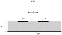
- FIG. 2 shows a cross-sectional view of the printed circuit board PCB, referred to as the main printed circuit board, produced at the coupling point CP, along an axis X of FIG. 1 .
- the coupling point CP of the main transmission line TL is situated in the same horizontal plane of the printed circuit board PCB as the coupling area CA of the secondary transmission line STL.
- the main transmission line TL (not represented) and the secondary transmission lines STL are conductive tracks integrated in the same printed circuit board PCB, which simplifies the production of the communications system.
- the main printed circuit board PCB is a multilayer printed circuit board and is composed of an external conductive track ECT made of copper which is electrically connected to a zero potential (0 V) of the printed circuit board in order to form a screen and thus limit the propagation of the radio waves.
- the printed circuit board PCB also includes external conductive tracks made of copper forming the main transmission line TL and the secondary transmission lines STL.
- the printed circuit board PCB may for example be manufactured with conductive layers, from which one of the copper layers are removed by trimming.
- the thickness of the external conductive tracks may be 35 ⁇ m, with a complete thickness of the printed circuit board of approximately 0.8 mm.
- the coupling area CA has for example a length of 5.9 mm and the distance d1 between the coupling point CP of the main transmission line TL and the coupling area CA of the secondary transmission line STL is for example 0.7 mm.
- the conductive track of the secondary transmission STL is preferably wider at the coupling area CA.
- FIG. 3 shows a cross-sectional view of the main printed circuit board PCB produced at a main antenna MA, along an axis Y of FIG. 1 .
- the communication module CM includes an auxiliary printed circuit board APCB, which has an auxiliary antenna AA similar to the main antenna MA, comprising a conductive layer made of copper that is placed on the upper portion of the auxiliary printed circuit board.
- the distance d2 between the main antenna MA and the auxiliary antenna is for example in the order of 1 cm.
- the radio communications between at least two communication modules CM will be made on one hand through the auxiliary antennas AA and respective main antennas MA and on the other hand through the directional coupling between the coupling areas AA (associated with said main antennas) and the main transmission line TL.
- the auxiliary antenna AA extends approximately perpendicular to the main antenna MA.
- FIG. 1 shows a simplified diagram showing an overview of the communication system
- the auxiliary antenna MA here included in the auxiliary printed circuit board APCB
- the main antenna MA of the printed circuit board PCB are therefore in two distinct planes, while the main transmission line TL and the coupling area CA of the secondary transmission line STL are in one and the same plane, as detailed clearly in FIG. 2 and FIG. 3 .
- the printed circuit board PCB can be mounted in a metal housing that surrounds the substrate and that includes a panel which sits on top of the main transmission line and presents holes above the main antennas allowing to place a communication module on the housing, such that the auxiliary antenna of the communication module is situated just above a main antenna.
- Some parts of the housing form a screen for the printed circuit board PCB to produce a close field for the main transmission line, acting like a faraday cage around the main transmission line.
- the printed circuit board PCB of the communication system can be incorporated in a backplane, for a very strong isolation of a modular industrial PLC, for example used as a bus for Input/Output modules or a redundant bus.
- the printed circuit board PCB of the communication system may be incorporated in routers of small size for homes with optical arrival and very high performance, or as a bus for information exchange inside an electrical panel (by lowering the frequency used by the antennas, the energy needed for communication can be drastically reduced).
- the printed circuit board PCB can be designed depending on the device it is incorporated in.
- the printed circuit board PCB should present an overall consistency between the length of the conductive tracks, the power of the transmitters and the number of main antennas for the main transmission line.
- the main transmission line is a passive electronic assembly with a defined shape which allows the waves to be distributed uniformly on all the main antennas. The shape and dimensions of the main transmission line and the main antennas can thus be defined for a desired spectrum of waves to be transmitted.
Landscapes
- Physics & Mathematics (AREA)
- Electromagnetism (AREA)
- Transceivers (AREA)
- Variable-Direction Aerials And Aerial Arrays (AREA)
- Waveguide Aerials (AREA)
- Mobile Radio Communication Systems (AREA)
Claims (8)
- Vorrichtung zur drahtlosen Kommunikation zwischen Kommunikationsmodulen (CM), wobei die Vorrichtung eine Hauptübertragungsleitung (TL) umfasst, die eine Vielzahl von Kopplungspunkten (CP) aufweist, wobei die Vorrichtung ferner eine Vielzahl von Hauptantennen (MA) umfasst, wobei jede Hauptantenne mit einem Kopplungsbereich (CA) zur gerichteten Kopplung zwischen der Hauptantenne und der Hauptübertragungsleitung an einem Kopplungspunkt der Vielzahl von Kopplungspunkten verbunden ist und jede Hauptantenne angepasst ist, um mit einer Hilfsantenne (AA) zu kommunizieren, die mit einem Kommunikationsmodul (CM) verbunden ist, dadurch gekennzeichnet, dass die Hauptübertragungsleitung (TL) zwei Abschlussimpedanzen (TI) mit Leitungsendimpedanzen gleich der charakteristischen Impedanz der Hauptübertragungsleitung (TL) aufweist.
- Vorrichtung nach Anspruch 1, wobei eine Hauptantenne (MA) der Vielzahl von Hauptantennen dafür ausgebildet ist, mit einer Hilfsantenne (AA) eines Kommunikationsmoduls in Verbindung zu stehen, wenn das Kommunikationsmodul über der Hauptantenne angeordnet ist.
- Vorrichtung nach einem der vorhergehenden Ansprüche, wobei die Hauptübertragungsleitung (TL) und die Hauptantennen (MA) Leiterbahnen sind, die in dieselbe Leiterplatte (PCB) integriert sind.
- Vorrichtung nach einem der vorhergehenden Ansprüche, wobei die Kopplungspunkte (CP) und die Kopplungsbereiche (CA) eine geradlinige Form haben.
- Vorrichtung nach einem der vorhergehenden Ansprüche, bei der jede Hauptantenne (MA) über eine sekundäre Übertragungsleitung (STL) mit einem Kopplungsbereich (CA) verbunden ist, wobei die Hauptantenne (MA) und die sekundäre Übertragungsleitung (STL) jeweils eine Abschlussimpedanz (TI) aufweisen, deren Leitungsendimpedanz gleich der charakteristischen Impedanz der sekundären Übertragungsleitung ist.
- Vorrichtung nach einem der vorhergehenden Ansprüche, wobei die Länge der Kopplungsbereiche von der Arbeitsfrequenz der Hauptantennen abhängt.
- Vorrichtung nach einem der vorhergehenden Ansprüche, wobei die Kopplungsbereiche gerichtete Kopplungen aufweisen, die kapazitiv und induktiv gekoppelt sind.
- Vorrichtung nach Anspruch 3, bei der die Leiterplatte (PCB) in einem Metallgehäuse montiert ist, das ein Substrat der Leiterplatte umgibt und eine Platte beinhaltet, die auf der Hauptübertragungsleitung (TL) sitzt und Löcher über den Hauptantennen (MA) der mehreren Hauptantennen aufweist, die es ermöglichen, ein Kommunikationsmodul (CM) auf dem Gehäuse zu platzieren, so dass sich die Hilfsantenne (AA) des Kommunikationsmoduls direkt über einer Hauptantenne der Vielzahl von Hauptantennen befindet.
Priority Applications (4)
| Application Number | Priority Date | Filing Date | Title |
|---|---|---|---|
| EP21306782.0A EP4199262B1 (de) | 2021-12-15 | 2021-12-15 | Backplane für drahtlose kommunikation |
| CN202211445555.8A CN116264344A (zh) | 2021-12-15 | 2022-11-18 | 无线通信背板 |
| JP2022185937A JP7840833B2 (ja) | 2021-12-15 | 2022-11-21 | ワイヤレス通信バックプレーン |
| US18/077,247 US12199368B2 (en) | 2021-12-15 | 2022-12-08 | Wireless communication backplane |
Applications Claiming Priority (1)
| Application Number | Priority Date | Filing Date | Title |
|---|---|---|---|
| EP21306782.0A EP4199262B1 (de) | 2021-12-15 | 2021-12-15 | Backplane für drahtlose kommunikation |
Publications (2)
| Publication Number | Publication Date |
|---|---|
| EP4199262A1 EP4199262A1 (de) | 2023-06-21 |
| EP4199262B1 true EP4199262B1 (de) | 2025-05-21 |
Family
ID=79021609
Family Applications (1)
| Application Number | Title | Priority Date | Filing Date |
|---|---|---|---|
| EP21306782.0A Active EP4199262B1 (de) | 2021-12-15 | 2021-12-15 | Backplane für drahtlose kommunikation |
Country Status (4)
| Country | Link |
|---|---|
| US (1) | US12199368B2 (de) |
| EP (1) | EP4199262B1 (de) |
| JP (1) | JP7840833B2 (de) |
| CN (1) | CN116264344A (de) |
Family Cites Families (9)
| Publication number | Priority date | Publication date | Assignee | Title |
|---|---|---|---|---|
| JPS61150504A (ja) * | 1984-12-25 | 1986-07-09 | Toshiba Corp | アンテナ装置 |
| US5404145A (en) * | 1993-08-24 | 1995-04-04 | Raytheon Company | Patch coupled aperature array antenna |
| US6061035A (en) * | 1997-04-02 | 2000-05-09 | The United States Of America As Represented By The Secretary Of The Army | Frequency-scanned end-fire phased-aray antenna |
| DE10021670A1 (de) * | 2000-05-05 | 2001-11-15 | Schleifring Und Appbau Gmbh | Vorrichtung zur breitbandigen elektrischen Signal- bzw. Energieübertragung mit Übertragungsstrecke mit Richtkopplern |
| US7952528B2 (en) * | 2007-09-04 | 2011-05-31 | Sierra Wireless, Inc. | Antenna configurations for compact device wireless communication |
| US20090122847A1 (en) * | 2007-09-04 | 2009-05-14 | Sierra Wireless, Inc. | Antenna Configurations for Compact Device Wireless Communication |
| US11652301B2 (en) * | 2018-04-11 | 2023-05-16 | Qualcomm Incorporated | Patch antenna array |
| KR102762884B1 (ko) * | 2020-03-25 | 2025-02-07 | 삼성전기주식회사 | 안테나 모듈 |
| FR3109042A1 (fr) * | 2020-04-01 | 2021-10-08 | Schneider Electric Industries Sas | Système de communication sans fil |
-
2021
- 2021-12-15 EP EP21306782.0A patent/EP4199262B1/de active Active
-
2022
- 2022-11-18 CN CN202211445555.8A patent/CN116264344A/zh active Pending
- 2022-11-21 JP JP2022185937A patent/JP7840833B2/ja active Active
- 2022-12-08 US US18/077,247 patent/US12199368B2/en active Active
Also Published As
| Publication number | Publication date |
|---|---|
| EP4199262A1 (de) | 2023-06-21 |
| JP2023088854A (ja) | 2023-06-27 |
| CN116264344A (zh) | 2023-06-16 |
| US12199368B2 (en) | 2025-01-14 |
| US20230187834A1 (en) | 2023-06-15 |
| JP7840833B2 (ja) | 2026-04-06 |
Similar Documents
| Publication | Publication Date | Title |
|---|---|---|
| EP3125368B1 (de) | In multipolarisationssubstrat integrierte wellenleiterantenne | |
| WO2019006394A1 (en) | DOS-TO-DOS OFFSETTING LAUNCH TOPOLOGY WITH DIAGONAL WAVEGUIDES | |
| CN109217905A (zh) | 用于近场通信系统的锥形同轴发射结构 | |
| EP1992081A2 (de) | Netzwerksteuerung | |
| US8232929B2 (en) | Microwave antenna for wireless networking of devices in automation technology | |
| AU2019274473B2 (en) | Millimeter wave phased array | |
| EP2416330A1 (de) | Modul von variabler kapazität und entsprechendes schaltmodul | |
| WO2012018500A1 (en) | Embedded printed edge-balun antenna system and method of operation thereof | |
| EP2441118B1 (de) | Verfahren zur erreichung intrinsischer sicherheitskonformität in drahtlosen geräten über isolierte überlappende erdungen und entsprechende vorrichtung | |
| CN106410405A (zh) | 电调天线馈电装置及方法 | |
| US12199368B2 (en) | Wireless communication backplane | |
| US11451264B2 (en) | Wireless communications system | |
| CN110915100A (zh) | 具有到模块的近场耦合的背板 | |
| CN103095353B (zh) | 波束赋形和多输入多输出多天线复用的切换系统 | |
| CN114361812B (zh) | Nfc天线组件、制作方法及电子设备 | |
| Piekarz et al. | 3D printed K-band air-filled waveguide directional coupler integrated with PCB using a through-patch transition | |
| KR101014472B1 (ko) | 밀집한 다층형 회로 | |
| KR20240170552A (ko) | 무선 시스템 | |
| US20240275043A1 (en) | Io-link wireless communication | |
| CN111384991A (zh) | 具有分区射频天线和匹配网络的装置以及相关方法 | |
| KR101970596B1 (ko) | 전자 장치 | |
| CN121011604A (zh) | 射频前端组件、射频收发系统、通信设备 | |
| Mazhar et al. | RF BASED INFORMATION ANNOUNCEMENT SYSTEM USING PIC MICROCONTROLLER |
Legal Events
| Date | Code | Title | Description |
|---|---|---|---|
| PUAI | Public reference made under article 153(3) epc to a published international application that has entered the european phase |
Free format text: ORIGINAL CODE: 0009012 |
|
| STAA | Information on the status of an ep patent application or granted ep patent |
Free format text: STATUS: THE APPLICATION HAS BEEN PUBLISHED |
|
| AK | Designated contracting states |
Kind code of ref document: A1 Designated state(s): AL AT BE BG CH CY CZ DE DK EE ES FI FR GB GR HR HU IE IS IT LI LT LU LV MC MK MT NL NO PL PT RO RS SE SI SK SM TR |
|
| STAA | Information on the status of an ep patent application or granted ep patent |
Free format text: STATUS: REQUEST FOR EXAMINATION WAS MADE |
|
| 17P | Request for examination filed |
Effective date: 20231219 |
|
| RBV | Designated contracting states (corrected) |
Designated state(s): AL AT BE BG CH CY CZ DE DK EE ES FI FR GB GR HR HU IE IS IT LI LT LU LV MC MK MT NL NO PL PT RO RS SE SI SK SM TR |
|
| GRAP | Despatch of communication of intention to grant a patent |
Free format text: ORIGINAL CODE: EPIDOSNIGR1 |
|
| STAA | Information on the status of an ep patent application or granted ep patent |
Free format text: STATUS: GRANT OF PATENT IS INTENDED |
|
| RIC1 | Information provided on ipc code assigned before grant |
Ipc: H01Q 9/04 20060101ALN20250210BHEP Ipc: H01Q 9/30 20060101ALN20250210BHEP Ipc: H01Q 21/08 20060101ALI20250210BHEP Ipc: H01Q 21/00 20060101AFI20250210BHEP |
|
| INTG | Intention to grant announced |
Effective date: 20250228 |
|
| GRAS | Grant fee paid |
Free format text: ORIGINAL CODE: EPIDOSNIGR3 |
|
| GRAA | (expected) grant |
Free format text: ORIGINAL CODE: 0009210 |
|
| STAA | Information on the status of an ep patent application or granted ep patent |
Free format text: STATUS: THE PATENT HAS BEEN GRANTED |
|
| AK | Designated contracting states |
Kind code of ref document: B1 Designated state(s): AL AT BE BG CH CY CZ DE DK EE ES FI FR GB GR HR HU IE IS IT LI LT LU LV MC MK MT NL NO PL PT RO RS SE SI SK SM TR |
|
| REG | Reference to a national code |
Ref country code: GB Ref legal event code: FG4D |
|
| REG | Reference to a national code |
Ref country code: CH Ref legal event code: EP |
|
| REG | Reference to a national code |
Ref country code: DE Ref legal event code: R096 Ref document number: 602021031071 Country of ref document: DE |
|
| REG | Reference to a national code |
Ref country code: IE Ref legal event code: FG4D |
|
| REG | Reference to a national code |
Ref country code: NL Ref legal event code: MP Effective date: 20250521 |
|
| PG25 | Lapsed in a contracting state [announced via postgrant information from national office to epo] |
Ref country code: PT Free format text: LAPSE BECAUSE OF FAILURE TO SUBMIT A TRANSLATION OF THE DESCRIPTION OR TO PAY THE FEE WITHIN THE PRESCRIBED TIME-LIMIT Effective date: 20250922 Ref country code: FI Free format text: LAPSE BECAUSE OF FAILURE TO SUBMIT A TRANSLATION OF THE DESCRIPTION OR TO PAY THE FEE WITHIN THE PRESCRIBED TIME-LIMIT Effective date: 20250521 Ref country code: ES Free format text: LAPSE BECAUSE OF FAILURE TO SUBMIT A TRANSLATION OF THE DESCRIPTION OR TO PAY THE FEE WITHIN THE PRESCRIBED TIME-LIMIT Effective date: 20250521 |
|
| REG | Reference to a national code |
Ref country code: LT Ref legal event code: MG9D |
|
| PG25 | Lapsed in a contracting state [announced via postgrant information from national office to epo] |
Ref country code: NO Free format text: LAPSE BECAUSE OF FAILURE TO SUBMIT A TRANSLATION OF THE DESCRIPTION OR TO PAY THE FEE WITHIN THE PRESCRIBED TIME-LIMIT Effective date: 20250821 Ref country code: GR Free format text: LAPSE BECAUSE OF FAILURE TO SUBMIT A TRANSLATION OF THE DESCRIPTION OR TO PAY THE FEE WITHIN THE PRESCRIBED TIME-LIMIT Effective date: 20250822 |
|
| PG25 | Lapsed in a contracting state [announced via postgrant information from national office to epo] |
Ref country code: NL Free format text: LAPSE BECAUSE OF FAILURE TO SUBMIT A TRANSLATION OF THE DESCRIPTION OR TO PAY THE FEE WITHIN THE PRESCRIBED TIME-LIMIT Effective date: 20250521 Ref country code: PL Free format text: LAPSE BECAUSE OF FAILURE TO SUBMIT A TRANSLATION OF THE DESCRIPTION OR TO PAY THE FEE WITHIN THE PRESCRIBED TIME-LIMIT Effective date: 20250521 |
|
| PG25 | Lapsed in a contracting state [announced via postgrant information from national office to epo] |
Ref country code: BG Free format text: LAPSE BECAUSE OF FAILURE TO SUBMIT A TRANSLATION OF THE DESCRIPTION OR TO PAY THE FEE WITHIN THE PRESCRIBED TIME-LIMIT Effective date: 20250521 |
|
| PG25 | Lapsed in a contracting state [announced via postgrant information from national office to epo] |
Ref country code: HR Free format text: LAPSE BECAUSE OF FAILURE TO SUBMIT A TRANSLATION OF THE DESCRIPTION OR TO PAY THE FEE WITHIN THE PRESCRIBED TIME-LIMIT Effective date: 20250521 |
|
| PG25 | Lapsed in a contracting state [announced via postgrant information from national office to epo] |
Ref country code: RS Free format text: LAPSE BECAUSE OF FAILURE TO SUBMIT A TRANSLATION OF THE DESCRIPTION OR TO PAY THE FEE WITHIN THE PRESCRIBED TIME-LIMIT Effective date: 20250821 |
|
| PG25 | Lapsed in a contracting state [announced via postgrant information from national office to epo] |
Ref country code: IS Free format text: LAPSE BECAUSE OF FAILURE TO SUBMIT A TRANSLATION OF THE DESCRIPTION OR TO PAY THE FEE WITHIN THE PRESCRIBED TIME-LIMIT Effective date: 20250921 |
|
| PG25 | Lapsed in a contracting state [announced via postgrant information from national office to epo] |
Ref country code: LV Free format text: LAPSE BECAUSE OF FAILURE TO SUBMIT A TRANSLATION OF THE DESCRIPTION OR TO PAY THE FEE WITHIN THE PRESCRIBED TIME-LIMIT Effective date: 20250521 |
|
| REG | Reference to a national code |
Ref country code: AT Ref legal event code: MK05 Ref document number: 1797625 Country of ref document: AT Kind code of ref document: T Effective date: 20250521 |
|
| PG25 | Lapsed in a contracting state [announced via postgrant information from national office to epo] |
Ref country code: SM Free format text: LAPSE BECAUSE OF FAILURE TO SUBMIT A TRANSLATION OF THE DESCRIPTION OR TO PAY THE FEE WITHIN THE PRESCRIBED TIME-LIMIT Effective date: 20250521 Ref country code: DK Free format text: LAPSE BECAUSE OF FAILURE TO SUBMIT A TRANSLATION OF THE DESCRIPTION OR TO PAY THE FEE WITHIN THE PRESCRIBED TIME-LIMIT Effective date: 20250521 Ref country code: AT Free format text: LAPSE BECAUSE OF FAILURE TO SUBMIT A TRANSLATION OF THE DESCRIPTION OR TO PAY THE FEE WITHIN THE PRESCRIBED TIME-LIMIT Effective date: 20250521 |
|
| PGFP | Annual fee paid to national office [announced via postgrant information from national office to epo] |
Ref country code: FR Payment date: 20251223 Year of fee payment: 5 |
|
| PG25 | Lapsed in a contracting state [announced via postgrant information from national office to epo] |
Ref country code: CZ Free format text: LAPSE BECAUSE OF FAILURE TO SUBMIT A TRANSLATION OF THE DESCRIPTION OR TO PAY THE FEE WITHIN THE PRESCRIBED TIME-LIMIT Effective date: 20250521 |
|
| PG25 | Lapsed in a contracting state [announced via postgrant information from national office to epo] |
Ref country code: EE Free format text: LAPSE BECAUSE OF FAILURE TO SUBMIT A TRANSLATION OF THE DESCRIPTION OR TO PAY THE FEE WITHIN THE PRESCRIBED TIME-LIMIT Effective date: 20250521 |
|
| PG25 | Lapsed in a contracting state [announced via postgrant information from national office to epo] |
Ref country code: SK Free format text: LAPSE BECAUSE OF FAILURE TO SUBMIT A TRANSLATION OF THE DESCRIPTION OR TO PAY THE FEE WITHIN THE PRESCRIBED TIME-LIMIT Effective date: 20250521 |
|
| PG25 | Lapsed in a contracting state [announced via postgrant information from national office to epo] |
Ref country code: IT Free format text: LAPSE BECAUSE OF FAILURE TO SUBMIT A TRANSLATION OF THE DESCRIPTION OR TO PAY THE FEE WITHIN THE PRESCRIBED TIME-LIMIT Effective date: 20250521 |
|
| REG | Reference to a national code |
Ref country code: DE Ref legal event code: R097 Ref document number: 602021031071 Country of ref document: DE |
|
| PG25 | Lapsed in a contracting state [announced via postgrant information from national office to epo] |
Ref country code: RO Free format text: LAPSE BECAUSE OF FAILURE TO SUBMIT A TRANSLATION OF THE DESCRIPTION OR TO PAY THE FEE WITHIN THE PRESCRIBED TIME-LIMIT Effective date: 20250521 |
|
| PLBE | No opposition filed within time limit |
Free format text: ORIGINAL CODE: 0009261 |
|
| STAA | Information on the status of an ep patent application or granted ep patent |
Free format text: STATUS: NO OPPOSITION FILED WITHIN TIME LIMIT |
|
| REG | Reference to a national code |
Ref country code: CH Ref legal event code: L10 Free format text: ST27 STATUS EVENT CODE: U-0-0-L10-L00 (AS PROVIDED BY THE NATIONAL OFFICE) Effective date: 20260402 |
|
| PGFP | Annual fee paid to national office [announced via postgrant information from national office to epo] |
Ref country code: DE Payment date: 20251229 Year of fee payment: 5 |
|
| 26N | No opposition filed |
Effective date: 20260224 |