EP4199067A1 - Ersatz über und vergrabene oder rückseitige stromschiene - Google Patents
Ersatz über und vergrabene oder rückseitige stromschiene Download PDFInfo
- Publication number
- EP4199067A1 EP4199067A1 EP22213221.9A EP22213221A EP4199067A1 EP 4199067 A1 EP4199067 A1 EP 4199067A1 EP 22213221 A EP22213221 A EP 22213221A EP 4199067 A1 EP4199067 A1 EP 4199067A1
- Authority
- EP
- European Patent Office
- Prior art keywords
- recess
- integrated circuit
- upper portion
- conductive material
- sub
- Prior art date
- Legal status (The legal status is an assumption and is not a legal conclusion. Google has not performed a legal analysis and makes no representation as to the accuracy of the status listed.)
- Pending
Links
Images


Classifications
-
- H—ELECTRICITY
- H10—SEMICONDUCTOR DEVICES; ELECTRIC SOLID-STATE DEVICES NOT OTHERWISE PROVIDED FOR
- H10W—GENERIC PACKAGES, INTERCONNECTIONS, CONNECTORS OR OTHER CONSTRUCTIONAL DETAILS OF DEVICES COVERED BY CLASS H10
- H10W20/00—Interconnections in chips, wafers or substrates
- H10W20/40—Interconnections external to wafers or substrates, e.g. back-end-of-line [BEOL] metallisations or vias connecting to gate electrodes
-
- H—ELECTRICITY
- H10—SEMICONDUCTOR DEVICES; ELECTRIC SOLID-STATE DEVICES NOT OTHERWISE PROVIDED FOR
- H10W—GENERIC PACKAGES, INTERCONNECTIONS, CONNECTORS OR OTHER CONSTRUCTIONAL DETAILS OF DEVICES COVERED BY CLASS H10
- H10W20/00—Interconnections in chips, wafers or substrates
- H10W20/01—Manufacture or treatment
- H10W20/021—Manufacture or treatment of interconnections within wafers or substrates
-
- H—ELECTRICITY
- H10—SEMICONDUCTOR DEVICES; ELECTRIC SOLID-STATE DEVICES NOT OTHERWISE PROVIDED FOR
- H10D—INORGANIC ELECTRIC SEMICONDUCTOR DEVICES
- H10D30/00—Field-effect transistors [FET]
- H10D30/60—Insulated-gate field-effect transistors [IGFET]
- H10D30/67—Thin-film transistors [TFT]
- H10D30/6729—Thin-film transistors [TFT] characterised by the electrodes
- H10D30/673—Thin-film transistors [TFT] characterised by the electrodes characterised by the shapes, relative sizes or dispositions of the gate electrodes
- H10D30/6735—Thin-film transistors [TFT] characterised by the electrodes characterised by the shapes, relative sizes or dispositions of the gate electrodes having gates fully surrounding the channels, e.g. gate-all-around
-
- H—ELECTRICITY
- H10—SEMICONDUCTOR DEVICES; ELECTRIC SOLID-STATE DEVICES NOT OTHERWISE PROVIDED FOR
- H10D—INORGANIC ELECTRIC SEMICONDUCTOR DEVICES
- H10D30/00—Field-effect transistors [FET]
- H10D30/60—Insulated-gate field-effect transistors [IGFET]
- H10D30/67—Thin-film transistors [TFT]
- H10D30/6757—Thin-film transistors [TFT] characterised by the structure of the channel, e.g. transverse or longitudinal shape or doping profile
-
- H—ELECTRICITY
- H10—SEMICONDUCTOR DEVICES; ELECTRIC SOLID-STATE DEVICES NOT OTHERWISE PROVIDED FOR
- H10D—INORGANIC ELECTRIC SEMICONDUCTOR DEVICES
- H10D62/00—Semiconductor bodies, or regions thereof, of devices having potential barriers
- H10D62/10—Shapes, relative sizes or dispositions of the regions of the semiconductor bodies; Shapes of the semiconductor bodies
- H10D62/117—Shapes of semiconductor bodies
- H10D62/118—Nanostructure semiconductor bodies
-
- H—ELECTRICITY
- H10—SEMICONDUCTOR DEVICES; ELECTRIC SOLID-STATE DEVICES NOT OTHERWISE PROVIDED FOR
- H10D—INORGANIC ELECTRIC SEMICONDUCTOR DEVICES
- H10D62/00—Semiconductor bodies, or regions thereof, of devices having potential barriers
- H10D62/10—Shapes, relative sizes or dispositions of the regions of the semiconductor bodies; Shapes of the semiconductor bodies
- H10D62/17—Semiconductor regions connected to electrodes not carrying current to be rectified, amplified or switched, e.g. channel regions
- H10D62/351—Substrate regions of field-effect devices
- H10D62/357—Substrate regions of field-effect devices of FETs
- H10D62/364—Substrate regions of field-effect devices of FETs of IGFETs
-
- H—ELECTRICITY
- H10—SEMICONDUCTOR DEVICES; ELECTRIC SOLID-STATE DEVICES NOT OTHERWISE PROVIDED FOR
- H10D—INORGANIC ELECTRIC SEMICONDUCTOR DEVICES
- H10D84/00—Integrated devices formed in or on semiconductor substrates that comprise only semiconducting layers, e.g. on Si wafers or on GaAs-on-Si wafers
- H10D84/01—Manufacture or treatment
- H10D84/0123—Integrating together multiple components covered by H10D12/00 or H10D30/00, e.g. integrating multiple IGBTs
- H10D84/0126—Integrating together multiple components covered by H10D12/00 or H10D30/00, e.g. integrating multiple IGBTs the components including insulated gates, e.g. IGFETs
- H10D84/0149—Manufacturing their interconnections or electrodes, e.g. source or drain electrodes
-
- H—ELECTRICITY
- H10—SEMICONDUCTOR DEVICES; ELECTRIC SOLID-STATE DEVICES NOT OTHERWISE PROVIDED FOR
- H10D—INORGANIC ELECTRIC SEMICONDUCTOR DEVICES
- H10D84/00—Integrated devices formed in or on semiconductor substrates that comprise only semiconducting layers, e.g. on Si wafers or on GaAs-on-Si wafers
- H10D84/01—Manufacture or treatment
- H10D84/02—Manufacture or treatment characterised by using material-based technologies
- H10D84/03—Manufacture or treatment characterised by using material-based technologies using Group IV technology, e.g. silicon technology or silicon-carbide [SiC] technology
- H10D84/038—Manufacture or treatment characterised by using material-based technologies using Group IV technology, e.g. silicon technology or silicon-carbide [SiC] technology using silicon technology, e.g. SiGe
-
- H—ELECTRICITY
- H10—SEMICONDUCTOR DEVICES; ELECTRIC SOLID-STATE DEVICES NOT OTHERWISE PROVIDED FOR
- H10D—INORGANIC ELECTRIC SEMICONDUCTOR DEVICES
- H10D84/00—Integrated devices formed in or on semiconductor substrates that comprise only semiconducting layers, e.g. on Si wafers or on GaAs-on-Si wafers
- H10D84/80—Integrated devices formed in or on semiconductor substrates that comprise only semiconducting layers, e.g. on Si wafers or on GaAs-on-Si wafers characterised by the integration of at least one component covered by groups H10D12/00 or H10D30/00, e.g. integration of IGFETs
- H10D84/82—Integrated devices formed in or on semiconductor substrates that comprise only semiconducting layers, e.g. on Si wafers or on GaAs-on-Si wafers characterised by the integration of at least one component covered by groups H10D12/00 or H10D30/00, e.g. integration of IGFETs of only field-effect components
- H10D84/83—Integrated devices formed in or on semiconductor substrates that comprise only semiconducting layers, e.g. on Si wafers or on GaAs-on-Si wafers characterised by the integration of at least one component covered by groups H10D12/00 or H10D30/00, e.g. integration of IGFETs of only field-effect components of only insulated-gate FETs [IGFET]
-
- H—ELECTRICITY
- H10—SEMICONDUCTOR DEVICES; ELECTRIC SOLID-STATE DEVICES NOT OTHERWISE PROVIDED FOR
- H10W—GENERIC PACKAGES, INTERCONNECTIONS, CONNECTORS OR OTHER CONSTRUCTIONAL DETAILS OF DEVICES COVERED BY CLASS H10
- H10W20/00—Interconnections in chips, wafers or substrates
- H10W20/01—Manufacture or treatment
- H10W20/031—Manufacture or treatment of conductive parts of the interconnections
- H10W20/056—Manufacture or treatment of conductive parts of the interconnections by filling conductive material into holes, grooves or trenches
-
- H—ELECTRICITY
- H10—SEMICONDUCTOR DEVICES; ELECTRIC SOLID-STATE DEVICES NOT OTHERWISE PROVIDED FOR
- H10W—GENERIC PACKAGES, INTERCONNECTIONS, CONNECTORS OR OTHER CONSTRUCTIONAL DETAILS OF DEVICES COVERED BY CLASS H10
- H10W20/00—Interconnections in chips, wafers or substrates
- H10W20/01—Manufacture or treatment
- H10W20/031—Manufacture or treatment of conductive parts of the interconnections
- H10W20/069—Manufacture or treatment of conductive parts of the interconnections by forming self-aligned vias or self-aligned contact plugs
- H10W20/0696—Manufacture or treatment of conductive parts of the interconnections by forming self-aligned vias or self-aligned contact plugs by using sacrificial placeholders, e.g. using sacrificial plugs
-
- H—ELECTRICITY
- H10—SEMICONDUCTOR DEVICES; ELECTRIC SOLID-STATE DEVICES NOT OTHERWISE PROVIDED FOR
- H10W—GENERIC PACKAGES, INTERCONNECTIONS, CONNECTORS OR OTHER CONSTRUCTIONAL DETAILS OF DEVICES COVERED BY CLASS H10
- H10W20/00—Interconnections in chips, wafers or substrates
- H10W20/20—Interconnections within wafers or substrates, e.g. through-silicon vias [TSV]
-
- H—ELECTRICITY
- H10—SEMICONDUCTOR DEVICES; ELECTRIC SOLID-STATE DEVICES NOT OTHERWISE PROVIDED FOR
- H10W—GENERIC PACKAGES, INTERCONNECTIONS, CONNECTORS OR OTHER CONSTRUCTIONAL DETAILS OF DEVICES COVERED BY CLASS H10
- H10W20/00—Interconnections in chips, wafers or substrates
- H10W20/40—Interconnections external to wafers or substrates, e.g. back-end-of-line [BEOL] metallisations or vias connecting to gate electrodes
- H10W20/41—Interconnections external to wafers or substrates, e.g. back-end-of-line [BEOL] metallisations or vias connecting to gate electrodes characterised by their conductive parts
- H10W20/425—Barrier, adhesion or liner layers
-
- H—ELECTRICITY
- H10—SEMICONDUCTOR DEVICES; ELECTRIC SOLID-STATE DEVICES NOT OTHERWISE PROVIDED FOR
- H10W—GENERIC PACKAGES, INTERCONNECTIONS, CONNECTORS OR OTHER CONSTRUCTIONAL DETAILS OF DEVICES COVERED BY CLASS H10
- H10W20/00—Interconnections in chips, wafers or substrates
- H10W20/40—Interconnections external to wafers or substrates, e.g. back-end-of-line [BEOL] metallisations or vias connecting to gate electrodes
- H10W20/41—Interconnections external to wafers or substrates, e.g. back-end-of-line [BEOL] metallisations or vias connecting to gate electrodes characterised by their conductive parts
- H10W20/427—Power or ground buses
-
- B—PERFORMING OPERATIONS; TRANSPORTING
- B82—NANOTECHNOLOGY
- B82Y—SPECIFIC USES OR APPLICATIONS OF NANOSTRUCTURES; MEASUREMENT OR ANALYSIS OF NANOSTRUCTURES; MANUFACTURE OR TREATMENT OF NANOSTRUCTURES
- B82Y10/00—Nanotechnology for information processing, storage or transmission, e.g. quantum computing or single electron logic
-
- H—ELECTRICITY
- H10—SEMICONDUCTOR DEVICES; ELECTRIC SOLID-STATE DEVICES NOT OTHERWISE PROVIDED FOR
- H10D—INORGANIC ELECTRIC SEMICONDUCTOR DEVICES
- H10D30/00—Field-effect transistors [FET]
- H10D30/01—Manufacture or treatment
- H10D30/014—Manufacture or treatment of FETs having zero-dimensional [0D] or one-dimensional [1D] channels, e.g. quantum wire FETs, single-electron transistors [SET] or Coulomb blockade transistors
-
- H—ELECTRICITY
- H10—SEMICONDUCTOR DEVICES; ELECTRIC SOLID-STATE DEVICES NOT OTHERWISE PROVIDED FOR
- H10D—INORGANIC ELECTRIC SEMICONDUCTOR DEVICES
- H10D30/00—Field-effect transistors [FET]
- H10D30/40—FETs having zero-dimensional [0D], one-dimensional [1D] or two-dimensional [2D] charge carrier gas channels
- H10D30/43—FETs having zero-dimensional [0D], one-dimensional [1D] or two-dimensional [2D] charge carrier gas channels having one-dimensional [1D] charge carrier gas channels, e.g. quantum wire FETs or transistors having 1D quantum-confined channels
-
- H—ELECTRICITY
- H10—SEMICONDUCTOR DEVICES; ELECTRIC SOLID-STATE DEVICES NOT OTHERWISE PROVIDED FOR
- H10D—INORGANIC ELECTRIC SEMICONDUCTOR DEVICES
- H10D62/00—Semiconductor bodies, or regions thereof, of devices having potential barriers
- H10D62/10—Shapes, relative sizes or dispositions of the regions of the semiconductor bodies; Shapes of the semiconductor bodies
- H10D62/117—Shapes of semiconductor bodies
- H10D62/118—Nanostructure semiconductor bodies
- H10D62/119—Nanowire, nanosheet or nanotube semiconductor bodies
- H10D62/121—Nanowire, nanosheet or nanotube semiconductor bodies oriented parallel to substrates
-
- H—ELECTRICITY
- H10—SEMICONDUCTOR DEVICES; ELECTRIC SOLID-STATE DEVICES NOT OTHERWISE PROVIDED FOR
- H10D—INORGANIC ELECTRIC SEMICONDUCTOR DEVICES
- H10D64/00—Electrodes of devices having potential barriers
- H10D64/20—Electrodes characterised by their shapes, relative sizes or dispositions
- H10D64/23—Electrodes carrying the current to be rectified, amplified, oscillated or switched, e.g. sources, drains, anodes or cathodes
- H10D64/251—Source or drain electrodes for field-effect devices
-
- H—ELECTRICITY
- H10—SEMICONDUCTOR DEVICES; ELECTRIC SOLID-STATE DEVICES NOT OTHERWISE PROVIDED FOR
- H10W—GENERIC PACKAGES, INTERCONNECTIONS, CONNECTORS OR OTHER CONSTRUCTIONAL DETAILS OF DEVICES COVERED BY CLASS H10
- H10W20/00—Interconnections in chips, wafers or substrates
- H10W20/01—Manufacture or treatment
- H10W20/031—Manufacture or treatment of conductive parts of the interconnections
- H10W20/032—Manufacture or treatment of conductive parts of the interconnections of conductive barrier, adhesion or liner layers
- H10W20/033—Manufacture or treatment of conductive parts of the interconnections of conductive barrier, adhesion or liner layers in openings in dielectrics
- H10W20/037—Manufacture or treatment of conductive parts of the interconnections of conductive barrier, adhesion or liner layers in openings in dielectrics the barrier, adhesion or liner layers being on top of a main fill metal
-
- H—ELECTRICITY
- H10—SEMICONDUCTOR DEVICES; ELECTRIC SOLID-STATE DEVICES NOT OTHERWISE PROVIDED FOR
- H10W—GENERIC PACKAGES, INTERCONNECTIONS, CONNECTORS OR OTHER CONSTRUCTIONAL DETAILS OF DEVICES COVERED BY CLASS H10
- H10W20/00—Interconnections in chips, wafers or substrates
- H10W20/01—Manufacture or treatment
- H10W20/031—Manufacture or treatment of conductive parts of the interconnections
- H10W20/0698—Local interconnections
Definitions
- Fabrication of microelectronic devices involves forming electronic components on microelectronic substrates, such as silicon wafers. These electronic components may include transistors, resistors, capacitors, and other active and passive devices, with overlying interconnect features (e.g., vias and lines) to route signals and power to and/or from the electronic components. Scaling of microelectronic devices results in high density of scaled interconnect features. To reduce congestion of interconnect features above the device layer comprising the electronic components, buried or backside power rail (BPR) architecture may be used. In some cases, BPR technology includes burying of conductors that deliver power (sometimes called power rails) to cells below the back end of line (BEOL) metal layers, usually in the same level as the device layer that includes semiconductor fins.
- BEOL back end of line
- BPR technology includes forming such power rails on the backside of the substrate underneath the device layer.
- Such BPR configurations free-up overhead to make more room for logic connections and enable further scaling of a standard logic cell (e.g., memory and logic cells).
- BPR configurations also allow for relatively larger power rails (e.g., thicker), which in turn exhibit lower resistance and power dissipation.
- power rails e.g., thicker
- Figs. 1A, 1B , 1C, 1D , 1E, and 1F illustrate various perspective, side, and plan views of an integrated circuit (IC) comprising a buried or backside power rail (BPR) structure including a first interconnect feature, wherein a second interconnect feature supplies power to the first interconnect feature, and a third interconnect feature provides power from the first interconnect feature to a terminal of a device, wherein the first, second, and third interconnect features collectively form a continuous and monolithic body of conductive material, and wherein a continuous conformal barrier layer is on the walls of the first, second, and third interconnect features, in accordance with an embodiment of the present disclosure.
- IC integrated circuit
- BPR backside power rail
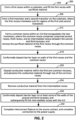
- Fig. 2 illustrates a flowchart depicting a method of forming an integrated circuit (such as the IC of Figs. 1A-1F ) comprising a BPR structure including a first interconnect feature, wherein a second interconnect feature supplies power to the first interconnect feature, and a third interconnect feature provides power from the first interconnect feature to a terminal of a device, wherein the first, second, and third interconnect features collectively form a continuous and monolithic body of conductive material, and wherein a continuous conformal barrier layer is on the walls of the first, second, and third interconnect features, in accordance with an embodiment of the present disclosure.
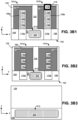
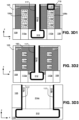
- Figs. 3A1, 3A2, 3A3 , 3B1, 3B2, 3B3 , 3C1, 3C2, 3C3 , 3C4 , 3D1, 3D2, 3D3 , 3E1, 3E2, 3E3 , 3F1, 3F2, 3F3 , 3G1, 3G2, 3G3 , 3H1, 3H2, and 3H3 illustrate various cross-sectional and perspective views of at least a section of an IC comprising the first, second, and third interconnect features of Figs. 1A-2 in various stages of processing, in accordance with an embodiment of the present disclosure.
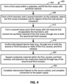
- Fig. 4 illustrates a flowchart depicting another method of forming an integrated circuit comprising a BPR structure including a first interconnect feature, wherein a second interconnect feature supplies power to the first interconnect feature, and a third interconnect feature provides power from the first interconnect feature to a terminal of a device, wherein the first, second, and third interconnect features collectively form a continuous and monolithic body of conductive material, and wherein a continuous conformal barrier layer is on the walls of the first, second, and third interconnect features, in accordance with an embodiment of the present disclosure.
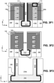
- Figs. 5A1, 5A2, 5A3 , 5B1, 5B2, 5B3 , 5C1, 5C2, 5C3 , 5D1,53D2, and 5D3 illustrate cross-sectional views of at least a section of an IC comprising the first, second, and third interconnect features of Figs. 1A-1E and 4 in various stages of processing, in accordance with an embodiment of the present disclosure.
- Fig. 6 illustrates a computing system implemented with integrated circuit structures having one or more interconnect features formed using the techniques disclosed herein, in accordance with some embodiments of the present disclosure.
- an integrated circuit structure including relatively low-resistance buried or backside power rail (BPR) is provided herein.
- an integrated circuit structure comprises a first sub-fin, and a second sub-fin laterally spaced from the first sub-fin by a distance of 100 nm or less.
- the integrated circuit structure further comprises a first transistor device over the first sub-fin and having a first contact, a second transistor device over the second sub-fin and having a second contact, and a continuous and monolithic body of conductive material extending vertically between the first and second transistor devices and the first and second sub-fins.
- the body of conductive material has (i) an upper portion between the first and second transistor devices and (ii) a lower portion between the first and second sub-fins, the lower portion being at least 1.2 times wider than the upper portion.
- the integrated circuit structure further comprises a continuous conformal layer that extends along a sidewall of the lower portion of the body and a sidewall of the upper portion of the body. In one such example, the continuous conformal layer does not separate the upper and lower portions of the body of conductive material.
- the integrated circuit structure further comprises a conductive interconnect feature connecting the upper portion of the body to at least one of the first and second contacts.
- an integrated circuit structure comprises a substrate, and one or more dielectric layers above the substrate.
- One or more transistors are on the substrate.
- a first recess is at least in part within the substrate, and a second recess and a third recess are at least in part within the one or more dielectric layers.
- a continuous monolithic body of conductive material is within the first recess, the second recess, and the third recess.
- a conductive interconnect feature couples the second recess with a terminal of a transistor of the one or more transistors.
- a method of forming interconnect features in an integrated circuit comprises forming a first recess within a substrate, depositing sacrificial material within the first recess, and forming (i) a first device having a first sub-fin region and (ii) a second device having a second sub-fin region.
- the first recess is laterally between the first sub-fin region and the second sub-fin region.
- dielectric material at least in part encapsulates the first and second devices.
- the method further comprises forming a second recess and a third recess within the dielectric material, where the second and third recesses lands on the first recess comprising the sacrificial material.
- the sacrificial material of the first recess is exposed through the second and third recesses.
- the method further comprises removing the sacrificial material of the first recess through any one or both the second and third recesses, and conformally depositing, through any one or both the second and third recesses, a barrier layer on walls of the first, second, and third recesses.
- the method further comprises depositing, through any one or both the second and third recesses, a monolithic and continuous body of conductive material within the first, second, and third recesses having the barrier layer on the walls.
- the method results in formation of a power rail within the first recess having the barrier layer and a first section of the body of conductive material, formation of a first interconnect feature within the second recess having the barrier layer and a second section of the body of conductive material, and formation of a second interconnect feature within the third recess having the barrier layer and a third section of the body of conductive material.
- a method of forming interconnect features in an integrated circuit comprises forming a first recess within a substrate, depositing sacrificial material within the first recess, and forming a first device having a first sub-fin region and a second device having a second sub-fin region.
- the first recess is laterally between the first sub-fin region and the second sub-fin region.
- dielectric material at least in part encapsulates the first and second devices.
- the method further comprises forming a common recess within the dielectric material. The common recess lands on the first recess comprising the sacrificial material.
- the common recess has a first section, a second section, and an intermediate section laterally between the first and second sections.
- the method further comprises removing the sacrificial material of the first recess through the common recess, conformally depositing a barrier layer on walls of the first and common recesses, and depositing a monolithic and continuous body of conductive material within the first and common recesses having the barrier layer on the walls.
- the method further comprises removing a portion of the body of conductive material from the intermediate section of the common recess, without removing conductive material from the first or second sections of the common recess.
- the method results in formation of a power rail within the first recess having a first section of the body of conductive material, formation of a first interconnect feature within the first section of the common recess having a second section of the body of conductive material, and formation of a second interconnect feature within the second section of the common recess having a third section of the body of conductive material.
- BPR backside power rails
- BPR-first integration scheme conductive material used for the BPR has to withstand high thermal budget during formation of the transistor, and such conductive material may have relatively high resistivity.
- barrier or liner layers between the BPR and other interconnect features add to the resistance.
- a BPR may be integrated after formation of the transistor (“BPR-last" integration scheme). While this BPR-last integration scheme enables use of materials that don't need to withstand high thermal budget during transistor gate stack formation, design rule limitations on the dimensions for the power rail result in relatively high resistance of the power rail.
- a dummy BPR is formed prior to integration of two adjacent transistors.
- the two transistors may be any appropriate type of nonplanar transistors, such as gate all around transistors in which the gate structure wraps around channel region comprising nanoribbons or nanosheets (or nanowires), or other nonplanar transistors such as forksheet transistors, FinFET transistors.
- Each transistor has a corresponding sub-fin region, and the dummy BPR is formed in a first recess within a substrate, where the first recess is laterally between the two sub-fin regions of the two transistors.
- the dummy BPR includes sacrificial material.
- the sacrificial material can be a material that can be selectively etched with respect to the material in which the recess is formed.
- the recess can be formed in an oxide (e.g., silicon dioxide), and the dummy BPR can be formed of a nitride (e.g., silicon nitride) or a carbide (e.g., silicon carbide).
- a second recess and a third recess are formed over the dummy BPR and within an interlayer dielectric (ILD) that encapsulates the two transistors, such that both the second and third recesses conjoin with the first recess of the dummy BPR.
- ILD interlayer dielectric
- the sacrificial material within the first recess of the dummy BPR is selectively removed through one or both the second and third recesses.
- the ILD layer in which the second and third recesses are formed can be the same material as the layer in which the recess in which the BPR was formed (e.g., such as silicon dioxide).
- a barrier layer (or liner layer or encapsulation layer) is conformally deposited on walls of the first, second, and third recesses, where the deposition is through the second and/or third recesses.
- the barrier layer is conformally deposited in a single process flow in the recesses. Accordingly, there is no seam or discontinuity between the barrier layer of the first recess, the barrier layer of the second recess, and the barrier layer of the third recess.
- the barrier layer can have a uniform width throughout the first, second, and third recesses. For example, a thickness of the barrier layer is in the range of about 0.5 to 4 nm and varies at most by 5% or 10% throughout the first, second, and third recesses.
- conductive material is deposited within the first, second, and third recesses during a single deposition process.
- conductive material is deposited within the first, second, and third recesses during a single deposition process.
- the second and third recesses are formed separately and remains separate during removal of the sacrificial material and deposition of the liner layer and the conductive material.
- a common big recess is formed that lands on the first recess, where the common recess includes a section for the second recess and another section for the third recess.
- sacrificial material of the first recess is selectively removed, and the continuous and conformal barrier layer and the monolithic conductive material are deposited through this common recess.
- conductive material and the barrier layer are selectively removed from a middle section of the common recess, and the resultant space is filed with interlayer dielectric (ILD) material, thereby separating the second and third recesses.
- ILD interlayer dielectric
- conductive material within the various recesses tends to diffuse through adjacent dielectric material.
- the diffusion may result in formation of undesirable copper oxide.
- the continuous and conformal barrier layer prevents diffusion of the conductive material (such as copper) to dielectric material adjacent to the recesses.
- the barrier layer facilitates better adhesion of the conductive material on walls of the recesses.
- the conductive material within the first recess forms the BPR.
- the conductive material within the second recess forms a first interconnect feature to receive power from a power supply source.
- conductive material within the third recess forms a second interconnect feature to supply the power to a terminal of one of the two transistors, such as a source, drain, or gate terminal of a transistor.
- the first recess comprising the BPR is laterally between the two sub-fin regions of the two transistors.
- the first interconnect feature supplying power from the power supply to the BPR extends vertically from the BPR, and extends above a level of the two transistors.
- the first interconnect feature routes power from the power supply to the BPR.
- the second interconnect feature supplying power to the terminal of one of the two transistors extends vertically from the BPR, and is laterally between the two transistors.
- the second interconnect feature supplying power to the terminal of one of the two transistors extends vertically from the BPR, and another horizontal interconnect feature between the second interconnect feature and the terminal supplies power from the second interconnect feature to the terminal.
- the conductive material of the power rail and the first and second interconnect features are deposited after completion of the adjacent transistors, the conductive material need not withstand high thermal budget of the transistor formation process. Accordingly, in an example, low thermal budget material having low resistance, such as copper, may be used for the conductive material. Additionally, the conductive material of the power rail and the first and second interconnect features is monolithic, without any seam or barrier layer therebetween, which reduces resistance between the power rail and the first and second interconnect features, thereby improving performance of the integrated circuit.
- compositionally different refers to two materials that have different chemical compositions. This compositional difference may be, for instance, by virtue of an element that is in one material but not the other (e.g., SiGe is compositionally different than silicon), or by way of one material having all the same elements as a second material but at least one of those elements is intentionally provided at a different concentration in one material relative to the other material (e.g., SiGe having 70 atomic percent germanium is compositionally different than from SiGe having 25 atomic percent germanium).
- the materials may also have distinct dopants (e.g., gallium and magnesium) or the same dopants but at differing concentrations.
- compositionally distinct materials may further refer to two materials that have different crystallographic orientations. For instance, (110) silicon is compositionally distinct or different from (100) silicon. Creating a stack of different orientations could be accomplished, for instance, with blanket wafer layer transfer. If two materials are elementally different, then one of the materials has an element that is not in the other material.
- Use of the techniques and structures provided herein may be detectable using tools such as electron microscopy including scanning/transmission electron microscopy (SEM/TEM), scanning transmission electron microscopy (STEM), nano-beam electron diffraction (NBD or NBED), and reflection electron microscopy (REM); composition mapping; x-ray crystallography or diffraction (XRD); energy-dispersive x-ray spectroscopy (EDX); secondary ion mass spectrometry (SIMS); time-of-flight SIMS (ToF-SIMS); atom probe imaging or tomography; local electrode atom probe (LEAP) techniques; 3D tomography; or high resolution physical or chemical analysis, to name a few suitable example analytical tools.
- tools such as electron microscopy including scanning/transmission electron microscopy (SEM/TEM), scanning transmission electron microscopy (STEM), nano-beam electron diffraction (NBD or NBED), and reflection electron microscopy (REM); composition mapping; x-ray crystallography or
- such tools may be used to detect a monolithic continuous body of conductive material of a BPR, a conductive interconnect feature to supply power to the BPR, and another conductive interconnect feature to transmit the power from the BPR to a terminal of a transistor; and continuous conformal barrier layer on walls of the BPR and the two conductive interconnect features.
- such tools may also be used to detect a location of the BPR relative to the transistor to which the power is being supplied. For example, the BPR is laterally between a sub-fin region of the transistor and a sub-fin region of another transistor.
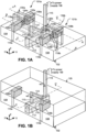
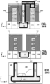
- Fig. 1A illustrates a perspective view of an integrated circuit (IC) 100 comprising a buried or backside power rail structure including a first interconnect feature 112, wherein a second interconnect feature 115 supplies power to the first interconnect feature 112, and a third interconnect feature 113 provides power from the first interconnect feature 112 to a terminal 116 of a device (such as a transistor) 101b, wherein at least the first, second, and third interconnect features collectively form a continuous and monolithic body of conductive material, and wherein a continuous conformal barrier layer 117 is on the walls of the first, second, and third interconnect features, in accordance with an embodiment of the present disclosure.
- IC integrated circuit
- FIG. 1B illustrates another perspective view of the various interconnect features of the integrated circuit 100 of Fig. 1A in further detail, in accordance with an embodiment of the present disclosure.
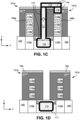
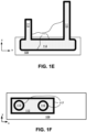
- Figs. 1C, 1D , and 1E illustrate side views of the integrated circuit 100 of Fig. 1A
- Fig. 1F illustrates a plan view of the first, second, and third interconnect features of the integrated circuit 100 of Fig. 1A , in accordance with an embodiment of the present disclosure.
- the cross-sectional view of Fig. 1C is along line B-B' of Fig. 1A
- the cross-sectional view of Fig. 1D is along line A-A' of Fig. 1A
- the cross-sectional view of Fig. 1E is along line C-C' of Figs. 1A and 1B .
- Fig. 1A does not illustrate some components of the IC 100, such as an interlayer dielectric (ILD) layer 125, which is illustrated in Fig. 1B .
- Fig. 1B illustrates only some components of the IC 100, such as various interconnect features, base or substrate 102, source/drain regions 106a, 106b, etc.
- ILD interlayer dielectric
- the IC 100 comprises devices 101a, 101b.
- the devices 101a, 101b are gate all around (GAA) transistors, such as nanoribbon transistors.
- GAA gate all around
- the devices 101a and/or 101b can be any other appropriate type of GAA transistors, such as nanowire transistors, nanosheet transistors.
- the devices 101a and/or 101b can be any other appropriate type of nonplanar transistors, such as forksheet transistors, FinFETs, or other appropriate type of transistors.
- the teachings of this disclosure are not limited to the devices 101a and/or 101b being any specific type of transistor(s).
- the device 101a has a source region 106a, a drain region 108a, and gate electrode 132a.
- the device 101b has a source region 106b, a drain region 108b, and gate electrode 132b.
- the devices 101a, 101b are formed on a base or substrate 102. Any number of semiconductor devices can be formed on the substrate 102, although only two such devices 101a, 101b are illustrated as an example.
- the substrate 102 can be, for example, a bulk substrate including group IV semiconductor material (such as silicon, germanium, or silicon germanium), group III-V semiconductor material (such as gallium arsenide, indium gallium arsenide, or indium phosphide), and/or any other suitable material upon which transistors can be formed.
- group IV semiconductor material such as silicon, germanium, or silicon germanium
- group III-V semiconductor material such as gallium arsenide, indium gallium arsenide, or indium phosphide
- any of the substrates can be a semiconductor-on-insulator (SOI) substrate having a desired semiconductor layer over a buried insulator layer (e.g., silicon over silicon dioxide).
- SOI semiconductor-on-insulator
- the substrate 102 can be a multilayer substrate or superlattice suitable for forming nanowires or nanoribbons (e.g., alternating layers of silicon and SiGe, or alternating layers indium gallium arsenide and indium phosphide). Any number of substrates can be used.
- Each of the devices 101a, 101b includes corresponding channel region laterally extending between and connecting corresponding source region 106 and drain region 108.
- the channel region includes two or more channel bodies, such as nanoribbons 118, that extend horizontally and are arranged in a vertical stack.
- the device 101a comprises a plurality of nanoribbons 118a extending laterally between corresponding source region 106a and drain region 108a
- the device 101b comprises a plurality of nanoribbons 118b extending laterally between corresponding source region 106b and drain region 108b.
- each of the devices 101a, 101b is illustrated to include three nanoribbons, the channel region of each of the devices can have any different number of nanoribbons, such as one, two, four, or higher.
- the present disclosure contemplates nanoribbons in a variety of configurations that include planar nanoribbon transistors, nanoribbons that extend vertically and are stacked horizontally, and other arrangements, as will be appreciated.
- the nanoribbons 118 comprise an appropriately doped semiconductor material, such as appropriately doped silicon. Note that in the side view of Fig. 1C the nanoribbons 118a, 118b would not be visible through the corresponding source regions 106a, 106b, respectively, and hence, the nanoribbons 118a, 118b are illustrated using dotted lines in Fig. 1C .
- the device 101a includes a sub-fin region 110a, above which the nanoribbons 118a of the device 101a are vertically stacked.
- the device 101b includes a sub-fin region 110b, above which the nanoribbons 118b of the device 101b are vertically stacked.
- sub-fin regions 110a, 110b comprise the same semiconductor material as the substrate 102.
- each device 101 may be separated from any adjacent device by a dielectric fill 109.
- Dielectric fill 109 provides shallow trench isolation (STI) between any adjacent semiconductor devices.
- Dielectric fill 109 can be any suitable dielectric material, such as silicon dioxide, aluminum oxide, or silicon oxycarbonitride.
- a gate structure 130a contacts and at least in part surrounds each nanoribbon 118a between the source and drain regions 106a, 108a, where the gate structure 130a includes gate dielectric (not illustrated), a gate electrode 132a, inner gate spacers (not illustrated), and gate spacers 134a.
- a gate structure 130b contacts and at least in part surrounds each nanoribbon 118b between the source and drain regions 106b, 108b, where the gate structure 130b includes gate dielectric (not illustrated), a gate electrode 132b, inner gate spacers (not illustrated), and gate spacers 134b.
- each nanoribbon 118 comprise a middle region between two end regions.
- a first end region of a nanoribbon is in contact with and abuts the corresponding source region and inner gate spacer
- a second end region of a nanoribbon is in contact with and abuts the corresponding drain region and inner gate spacer.
- the dielectric layer wraps around the middle region of individual nanoribbons, but doesn't wrap around the end regions of individual nanoribbons.
- the gate electrode 132a extends over and wraps around the nanoribbons 118a in the device 101a
- the gate electrode 132b extends over and wraps around the nanoribbons 118b in the device 101b.
- Gate electrodes 132a, 132b may include any sufficiently conductive material such as a metal, metal alloy, or doped polysilicon. Although not illustrated, in each of the devices 101a, 101b, the gate structure also includes inner gate spacers that is laterally between and that separate the corresponding source region and the corresponding gate electrode, as well as laterally between and that separate the corresponding drain region and the corresponding gate electrode.
- the device 101a comprises the sub-fin region 110a and the device 101b comprises the sub-fin region 110b.
- the two sub-fin regions 110a, 110b are spaced from each other by a distance of 200 nm or less, 150 nm or less, 100 nm or less, 50 nm or less, 25 nm or less, 15 nm or less, 10 nm or less, or between 5-8 nm or less.
- at least a section of the interconnect feature 112 is laterally between the first and second sub-fin regions 110a, 110b.
- the interconnect feature 112 thus, is buried at or below a level of the transistor devices 110a, 110b.
- the interconnect feature 112 is buried within or below a device layer of the IC 100.
- various interconnect features 112, 113, 114, 115, and 116 illustrated in Figs. 1A-1F are to supply power to the source 106b of the device 101b.
- the interconnect features may instead supply power to any other terminal of the devices 101a, 101b, such as the source 106a, drain 108a, or gate electrode 132a of the device 101a, or the drain 108b or gate electrode 132b of the device 101b.
- the interconnect feature 112 is a buried or backside power rail (BPR), as the interconnect feature 112 is a power rail supplying power to a terminal (e.g., source 106a) of the device 101b and as the interconnect feature 112 is buried within or underneath a device layer of the IC 100.
- BPR backside power rail
- the interconnect feature 112 is buried within the substrate 102 at, for example, a sub-fin level of the devices 101a, 101b.
- the interconnect feature 112 receives power from a power supply 190 (not illustrated), through the interconnect feature 115.
- the interconnect feature 112 provides the power to the source region 106b of the device 101b, e.g., through a vertical interconnect feature 113.
- a source contact 116 is coupled to the source region 106b.
- a horizontal interconnect feature 114 couples the interconnect feature 113 with the source contact 116.
- the interconnect feature 112 supplies power form the power supply 190 to the source region 106b, through the interconnect features 115, 113, 114, and the source contact 116.
- the interconnect features 112, 113, 115 have widths of w1, w2, and w3, respectively, where the widths are labelled in Figs. 1B and 1C .
- the widths w1, w2, w3 are measured in a direction that is perpendicular to a length of nanoribbons 118a, 118b of the devices 100a, 100b.
- the width w1 is greater than w2.
- the width w1 is greater than w3.
- w1 is at least 110% greater, at least 120% greater, at least 140% greater, at least 150% greater, at least 180% greater, or at least 200% greater than the width w2.
- w1 is at least 110% greater, at least 120% greater, at least 140% greater, at least 150% greater, at least 180% greater, or at least 200% greater than the width w3.
- the interconnect feature 112 is wider than the interconnect features 113 and/or 115.
- the width w1 is substantially similar to the widths w2 and/or w3. In an example, the width w1 is within 1%, 2%, 5%, 10%, or 20% of one or both the widths w2 or w3.
- the interconnect features 112, 113, 114, and 115 comprise suitable conductive material, such as pure copper, ruthenium, molybdenum, tungsten, an alloy such as copper-tin (CuSn), copper indium (CuIn), copper-antimony (CuSb), aluminum, copper-bismuth (CuBi), copper-rhenium (CuRe), and/or any other suitable conductive material.
- suitable conductive material such as pure copper, ruthenium, molybdenum, tungsten, an alloy such as copper-tin (CuSn), copper indium (CuIn), copper-antimony (CuSb), aluminum, copper-bismuth (CuBi), copper-rhenium (CuRe), and/or any other suitable conductive material.
- the interconnect features 112, 113, and 115 comprise a continuous and monolithic body of conductive material. For example, there is no seam, barrier layer, liner layer, or capping layer between the conductive materials of the interconnect features 112, 113, and 115. For example, because of the manner in which the interconnect features 112, 113, and 115 are formed, as will be discussed herein later, conductive materials of these interconnect features 112, 113, and 115 are formed without any barrier or capping layers therebetween.
- barrier layers 117 and/or 119 may be present between the conductive materials of the interconnect features 113 and 114, and between the conductive materials of the interconnect features 114 and 116.
- the barrier layer 117 may be absent between the conductive materials of the interconnect features 113 and 114, and/or between the conductive materials of the interconnect features 114 and 116
- barrier layer 117 extends along the walls of the interconnect features 112, 113, and 115.
- layer 119 extends along the walls of the interconnect features 114 and 116.
- the layer 117 on walls of the interconnect features 112, 113, 115 is a continuous and conformal layer.
- the layer 117 on walls of the interconnect features 112, 113, 115 may be formed during a single conformal deposition process, and hence, is a continuous and conformal layer.
- the layer 117 on walls of the interconnect features 112, 113, 115 and the layer 119 of the walls of the interconnect features 114 and 116 may be formed at different deposition processes. Accordingly, the layer 117 and the layer 119 may, or may not, be conformal and continuous. However, as discussed, as the layer 117 on walls of the interconnect features 112, 113, 115 may be formed during a single conformal deposition process, the layer 117 is a continuous and conformal layer. Note that while Fig. 1C-1F illustrate the layers 117, 119, these layers are not illustrated in Figs. 1A-1B for purposes of illustrative clarity.
- the layer 117 is on a top wall of the interconnect feature 112.
- the layer 117 on the top wall of the interconnect feature 112 is not illustrated, and instead the conductive material of the interconnect feature 112 underneath the layer 117 on top wall is illustrated.
- the layer 117 is on sidewalls, bottom surface, and top wall of the interconnect feature 112.
- the layer 117 is on sidewalls and top wall of the interconnect feature 113. Note that the bottom surface of the interconnect feature 113 is on the interconnect feature 112 (see Figs.
- the layer 117 is absent on the bottom surface of the interconnect feature 113.
- the layer 117 is absent between the conductive materials of the interconnect features 112, 113.
- the layer 117 is on sidewalls and top wall of the interconnect feature 115.
- the bottom surface of the interconnect feature 115 is on the interconnect feature 112 (see Figs. 1A, 1B , and 1E ), and the layer 117 is absent on the bottom surface of the interconnect feature 115.
- the layer 117 is absent between the conductive materials of the interconnect features 112, 115.
- the layer 119 is on top walls, bottom walls, and sidewalls of the interconnect features 114 and 116.
- the layers 117, 119 act as a liner or barrier layer, as well as a capping (or encapsulation) layer.
- conductive material within various interconnect features tends to diffuse through adjacent dielectric material.
- the diffusion may result in formation of undesirable copper oxide.
- the layers 117, 119 prevents diffusion of the conductive material (such as copper) to dielectric material adjacent to the interconnect features.
- the layers 117, 119 facilitate better adhesion of the conductive material on walls of the interconnect features.
- each of the layers 117, 119 has a width or thickness in the range of 1 to 5 nanometers (nm), or 1 to 10 nm, or 0.5 to 10 nm.
- Suitable materials for the layers 117, 119 include barrier layer refractory metals and alloys, cobalt, cobalt-nickel (CoNi), ruthenium-cobalt combination, molybdenum, nickel, manganese, titanium-tungsten (Ti ), tantalum (Ta), tantalum-nitride (TaN), tantalum-silicon-nitride (TaSiN), titanium-nitride (TiN), titanium-silicon-nitride (TiSiN), tungsten (XV), tungsten-nitride (WN), tungsten-silicon-nitride (WiSiN), and/or combinations of such materials (e.g., a multi-lay stack of Ta/TaN).
- the layers 117, 119 are absent between the junction of the conductive materials of the two conjoined interconnect features.
- the interconnect features 112, 113 form a continuous and monolithic body of conductive material extending vertically between the devices 101a, 101b, where the devices 101a, 101b have sub-fin regions 110a, 110b, respectively.
- the continuous and monolithic body of conductive material has an upper portion between the devices 101a, 101b, and a lower portion between the sub-fin regions 101a, 101b.
- the upper portion comprises at least a section of the interconnect feature 113
- the lower portion comprises at least a section of the interconnect feature 112.
- the width w1 of the lower portion i.e., the interconnect feature 112 is greater than the width w2 of the upper portion (i.e., the interconnect feature 113) by, for example, is at least 110%, at least 120%, at least 140%, at least 150%, at least 180%, or at least 200%.
- the interconnect feature 112 comprises a buried or backside power rail (BPR) of the IC 100.
- BPR backside power rail
- the interconnect feature 112 is buried at the sub-fin level of the devices 101a, 101b.
- the power rail is buried at least in part on the backside of the devices 101a, 101b, e.g., within and/or underneath a device layer of the IC 100. Having the power rail buried in the sub-fin region or otherwise on the backside of the devices 101a, 101b resolves mid end of line (MEOL) and/or back end of line (BEOL) metal congestion in the IC 100.
- MEOL mid end of line
- BEOL back end of line
- the IC 100 comprises an interlayer dielectric (ILD) layer 125 at least in part encapsulating the devices 101a, 101b and the interconnect features 113, 114, 116, and at least a section of the interconnect feature 115.
- ILD interlayer dielectric
- the substrate 102 encapsulates the interconnect feature 112.
- the interconnect feature 115 traverses through the ILD 125, and also extends through MEOL and/or BEOL of the IC device 100 (the MEOL and/or BEOL are not illustrated).
- the interconnect feature 115 and/or other interconnect features coupled to the interconnect feature 115 traverse through one or more interconnect layers and metallization levels of the MEOL and/or BEOL.
- each of the interconnect features 112, 113, 114, 115, and 116 are formed on corresponding recesses (formation of at least some of which are discussed herein later in turn).
- a first recess of the interconnect feature 112 is conjoined with a second recess of the interconnect feature 113 at one end, and a third recess of the interconnect feature 115 at another end.
- the second recess comprising the interconnect feature 113 is coupled to a terminal (e.g., a source 106b) of one of the devices 101a, 101b, via the interconnect feature 114.
- the third recess comprising the interconnect feature 115 is coupled to the power supply 190.
- the first, second, and third recesses comprise the monolithic continuous body of conductive material of the interconnect features 112, 113, 115.
- the continuous and conformal layer 117 is on walls of the first, second, and third recesses, where the layer 117 is a barrier/ liner/encapsulation layer.
- Fig. 2 illustrates a flowchart depicting a method 200 of forming an integrated circuit (such as the IC 100 of Figs. 1A-1F ) comprising a BPR structure including a first interconnect feature (e.g., interconnect feature 112), wherein a second interconnect feature (e.g., second interconnect feature 115) supplies power to the first interconnect feature, and a third interconnect feature (e.g., second interconnect feature 113) provides power from the first interconnect feature to a terminal of a device (such as a transistor 101b), wherein the first, second, and third interconnect features collectively form a continuous and monolithic body of conductive material, and wherein a continuous conformal barrier layer (e.g., barrier layer 117) is on the walls of the first, second, and third interconnect features, in accordance with an embodiment of the present disclosure.
- a first interconnect feature e.g., interconnect feature 112
- a second interconnect feature e.g., second interconnect feature
- Figs. 3A1, 3A2, 3A3 , 3B1, 3B2, 3B3 , 3C1, 3C2, 3C3 , 3C4 , 3D1, 3D2, 3D3 , 3E1, 3E2, 3E3 , 3F1, 3F2, 3F3 , 3G1, 3G2, 3G3 , 3H1, 3H2, and 3H3 illustrate cross-sectional and perspective views of at least a section of an IC comprising the first, second, and third interconnect features of Figs. 1A-2 in various stages of processing, in accordance with an embodiment of the present disclosure.
- Figs. 2 and 3A1-3H3 will be discussed in unison.
- Figs. 3A1 , 3B1 , 3C1 , and so on illustrate the cross-sectional view along line B-B' of Fig. 1A (i.e., a view similar to the view of Fig. 1C ).
- Figs. 3A2 , 3B2 , 3C2 , and so on illustrate the cross-sectional view along line A-A' of Fig. 1A (i.e., a view similar to the view of Fig. 1D ).
- Figs. 3A3 , 3B3 , 3C3 , and so on illustrate the side view along line C-C' of Fig. 1A (i.e., a view similar to the view of Fig. 1E ).
- Fig. 3C4 illustrates a perspective view, and illustrates only some components of the IC 100, e.g., similar to the view of Fig. 1B .
- the method 200 comprises forming a first recess within a substrate and filling the first recess with sacrificial material.
- Figs. 3A1-3A3 illustrate a first recess 312 formed within the substrate 102, where the first recess 312 is filled with sacrificial material 305.
- the method 200 proceeds from 204 to 208, where a first transistor and a second transistor are formed on the substrate, and where the first recess is between sub-fin regions of the first and second transistors.
- Figs. 3B1 and 3B2 illustrate transistors 101a, 101b formed on the substrate 102, where the recess 312 is laterally between sub-fin regions 110a, 110b of transistors 101a, 101b, respectively. Structure of the transistors 101a, 101b have been discussed herein previously. Formation of the two transistors 101a, 101b can be performed using any suitable techniques for forming transistors.
- the method 200 proceeds then from 208 to 212, where a common recess is formed within an ILD that encapsulates the two transistors, where the common recess comprises conjoined second recess, third recess, and an intermediate recess between the second and third recesses.
- the common recess exposes the sacrificial material of the first recess. Subsequently, sacrificial material of the first recess is removed through the common recess.
- Figs. 3C1, 3C2, 3C3 , and 3C4 illustrate the common recess 314 within ILD 125, where the common recess 314 exposes the sacrificial material 305 of the first recess 312.
- Fig. 3C3 illustrates boundaries of the second recess 314a, third recess 314b, and the intermediate recess 314c between the second and third recesses. Note that there are no physical boundaries between the second, third, and intermediate recesses - rather, there is a single common recess 314. Hence, the boundaries between these recesses are drawn with doted lines in Fig. 3C3 .
- An appropriate etching technique may be used to form the common recess, such as an anisotropic etch process, in which a mask is used to selectively remove the ILD 125 and form the common recess.
- Fig. 3C1 illustrates the second recess 314a that extends between the source regions 106a, 106b.
- the view of Fig. 3C2 illustrates the intermediate recess 314c that at least in part extends between the gate electrodes 132a and 132b of the two devices.
- the third recess 314b is not visible in either of the views of Figs. 3C1 or 3C2 , but is visible in the view of Fig. 3C3 .
- sacrificial material 305 of the first recess 312 is removed through the common recess 314, and hence, the first recess 312 is shown to not include the sacrificial material 305 in Figs. 3C1-3C4 .
- An appropriate etching technique may be used to remove the sacrificial material 305, such as an isotropic etch process (e.g., nitric acid/hydrofluoric acid) or another suitable etch process.
- a barrier layer is conformally deposited on walls of the first recess and the common recess.
- Figs. 3D1, 3D2, and 3D3 illustrate the barrier layer 117 conformally deposited on the walls of the first recess 312 and the common recess 314.
- atomic layer epitaxy, CVD, PVD, ALD, VPE, MBE, LPE, or other suitable conformal deposition technique is used to deposit the barrier layer 117 on the walls of the recesses.
- the method 200 then proceeds from 216 to 220, where conductive material is deposited within the first and common recesses, and the conductive material is planarized through top of the common recess.
- conductive material is deposited within the first and common recesses, and the conductive material is planarized through top of the common recess.
- Figs. 3E1, 3E2, and 3E3 illustrate conductive material deposited within the first recess 312 and the common recesses 314, and planarized through a top of the common recesses 314.
- deposition of the conductive material includes forming a seed layer (not illustrated in the figures) of conductive material on the barrier layer 117.
- the seed layer may be formed by a deposition process such as atomic layer epitaxy, CVD, PVD, ALD, VPE, MBE, LPE, via electroplating, e.g., in order to improve subsequent deposition of conductive material.
- one or more monolayers of seed material may be used.
- the seed layer may be deposited using an electroless deposition.
- the seed material is to be subsequently used for an electroplating deposition.
- the seed layer comprises copper (Cu) or an alloy of copper (e.g., copper-tin (CuSn), copper-indium (CuIn), copper-magnesium (CuMg), copper-aluminum (CuAl)), cobalt, and/or the like, e.g., to assist with a subsequent formation of a copper containing conductive material thereon.
- the process of seed layer formation may be performed if the final conductive material to be deposited in the recesses include copper or another appropriate metal or metal alloy that is to be electroplated. For example, if the final conductive material include copper, then the copper is to be deposited using an electroplating process on the seed layer. The seed layer is used to facilitate the electroplating process.
- the process of forming the seed layer can be skipped in an example.
- ruthenium may be used as the conductive material and may be deposited using ALD, and hence, deposition of ruthenium may not necessitate the formation of the seed layer.
- the conductive material comprising metal may be deposited via electroplating.
- electroless deposition, CVD, PVD, ALD or another suitable deposition technique may be used, e.g., when the conductive material comprises ruthenium or another appropriate conductive material.
- the conductive material is planarized from the top surface of the common recess 314, e.g., using CMP (chemical mechanical polishing), mechanical polishing, or another suitable planarization technique.
- CMP chemical mechanical polishing
- mechanical polishing or another suitable planarization technique.
- the first recess 312 and the common recess 314 are filled with the conductive material during the same deposition process.
- the conductive material is continuous and monolithic within both the recesses 312, 314.
- the method 200 proceeds from 220 to 224, where the conductive material from the intermediate section 314c of the common recess 314 is removed, e.g., without removing the conductive material within the first recess 312, the second recess 314a, and the third recess 314b, as illustrated in Figs. 3F1, 3F2, and 3F3 .
- sections of the layer 117 on walls of the intermediate section 314c of the common recess 314 are also removed, as illustrated in Fig. 3F2 .
- An appropriate etching technique may be used to remove the conductive material and/or the barrier layer 117 from the intermediate recess 314c, such as an anisotropic etch process, in which a mask is used to cover the recesses 314a and 314b and expose the recess 314c.
- the method 200 proceeds from 224 to 228, where barrier layer 117 is deposited on at least some of the walls of the second and third recesses, and then the intermediate recess is filed with the ILD.
- the removal of the conductive material during process 224 exposes some of the walls of the second recess 314a and third recess 314b, which were facing the intermediate recess 314c, and the barrier layer 117 is deposited on these exposed walls.
- Figs. 3G1, 3G2, 3G3 illustrate the barrier layer 117 is deposited on these exposed walls.
- the intermediate recess 312c is filled with the ILD 125, as seen in Figs. 3G2 and 3G3 . This completes the formation of the interconnect feature 112 within the recess 312, formation of the interconnect feature 113 within the recess 314a, and formation of the interconnect feature 115 within the recess 314b.
- the method 200 then proceeds from 228 to 232, where the interconnect feature 114 between the interconnect feature 113 and the source contact 116 is completed, and a connection between the interconnect feature 115 and the power supply 190 is complete.
- Figs. 3H1, 3H2, and 3H3 illustrate the interconnect feature 114 between the interconnect feature 113 and the source contact 116. Connection to the power supply 190 is not illustrated in these figures, although such a connection has been discussed with respect to Figs. 1A and 1B .
- the method 200 of Fig. 2 includes formation of a common recess 314, and later conductive material from sections of the common recess 314 is removed and filed with ILD 125, to thereby separate the second and third recesses 314a, 314b.
- method 400 of Fig. 4 includes separately forming a second recess and a third recess for the interconnect features 113 and 115, respectively.
- no common recess is formed - instead, the second recess and the third recess are separate from the beginning.
- Fig. 4 illustrates another flowchart depicting a method 400 of forming an integrated circuit (such as the IC 100 of Figs. 1A-1F ) comprising a BPR structure including a first interconnect feature (e.g., interconnect feature 112), wherein a second interconnect feature (e.g., second interconnect feature 115) supplies power to the first interconnect feature, and a third interconnect feature (e.g., second interconnect feature 113) provides power from the first interconnect feature to a terminal of a device (such as a transistor 101b), wherein at least the first, second, and third interconnect features collectively form a continuous and monolithic body of conductive material, and wherein a continuous conformal barrier layer (e.g., barrier layer 117) is on the walls of the first, second, and third interconnect features, in accordance with an embodiment of the present disclosure.
- a first interconnect feature e.g., interconnect feature 112
- a second interconnect feature e.g., second interconnect
- Figs. 5A1, 5A2, 5A3 , 5B1, 5B2, 5B3 , 5C1, 5C2, 5C3 , 5D1 ,53D2, and 5D3 illustrate cross-sectional views of at least a section of an IC comprising the first, second, and third interconnect features of Figs. 1A-1E and 4 in various stages of processing, in accordance with an embodiment of the present disclosure.
- Figs. 4 and 5A1-5D3 will be discussed in unison.
- Operations 404 and 408 of the method 400 of Fig. 4 are similar to operations 204 and 208 of the method 200 of Fig. 2 , respectively, and hence, operations 404 and 408 are not discussed in further detail herein.
- the structures illustrated in Figs. 5A1-5A3 are formed, where Figs. 5A1-5A3 are similar to Figs. 3B1-3B3 discussed herein earlier.
- the method 400 then proceeds from 408 to 412, where a second recess 514a and a third recess 514b are formed within ILD 125, and the sacrificial material 305 of the first recess is removed through one or both the second and third recesses.
- Figs. 5B1, 5B2, 5B3 illustrate the second recess 514a and the third recess 514b that lands on the first recess 312.
- the sacrificial material within the first recess 312 is exposed through the second recess 514a and the third recess 514b.
- An appropriate etching technique may be used to form the two recesses, such as an anisotropic etch process, in which a mask is used to selectively remove the ILD 125 and form the two recess.
- the sacrificial material 305 of the first recess 312 is then removed through one or both the second and third recesses using a suitable etching technique, such as an isotropic etch process (e.g., nitric acid/hydrofluoric acid) or another suitable etch process.
- a suitable etching technique such as an isotropic etch process (e.g., nitric acid/hydrofluoric acid) or another suitable etch process.
- the method 400 then proceeds from 412 to 416, where a barrier layer is deposited on walls of the first recess 312, second recess 514a, and third recess 514b.
- the barrier layer 117 is conformally deposited through any one or both the second and/or third recesses.
- Figs. 5C1, 5C2, 5C3 illustrate the barrier layer 117 on walls of the recesses 312, 514a, 514b.
- atomic layer epitaxy, CVD, PVD, ALD, VPE, MBE, LPE, or other suitable conformal deposition technique is used to deposit the barrier layer 117 on the walls of the recesses.
- the method 400 then proceeds from 416 to 420, where conductive material is deposited within the first, second, and third recesses, and the conductive material is planarized through top of the second and third recesses.
- a capping or encapsulation layer may be formed on top surface of the second and third recesses, as illustrated in Figs. 5D1 and 5D3 .
- Processes associated with deposition of conductive material have been discussed in detail with respect to process 200 of method 200.
- Figs. 5D1, 5D2, and 5D3 illustrate the recesses, with conductive material therewithin. As all three recesses are filled with the conductive material during the same deposition process, the conductive material is continuous and monolithic within both the recesses 312, 514a, 514b.
- the method 400 proceeds from 420 to 424, where the interconnect feature 114 between the interconnect feature 113 and the source contact 116 is completed, and a connection between the interconnect feature 115 and the power supply 190 is complete.
- Figs. 3H1, 3H2, and 3H3 illustrate the interconnect feature 114 between the interconnect feature 113 and the source contact 116. Connection to the power supply 190 is not illustrated in these figures, although such a connection has been discussed with respect to Figs. 1A and 1B .
- method 400 is shown in a particular order for ease of description. However, one or more of the processes may be performed in a different order or may not be performed at all (and thus be optional), in accordance with some embodiments. Numerous variations on method 400 and the techniques described herein will be apparent in light of this disclosure.
- Fig. 6 illustrates a computing system 1000 implemented with integrated circuit structures and/or the interconnect features formed using the techniques disclosed herein, in accordance with some embodiments of the present disclosure.
- the computing system 1000 houses a motherboard 1002.
- the motherboard 1002 may include a number of components, including, but not limited to, a processor 1004 and at least one communication chip 1006, each of which can be physically and electrically coupled to the motherboard 1002, or otherwise integrated therein.
- the motherboard 1002 may be, for example, any printed circuit board, whether a main board, a daughterboard mounted on a main board, or the only board of system 1000, etc.
- computing system 1000 may include one or more other components that may or may not be physically and electrically coupled to the motherboard 1002.
- these other components may include, but are not limited to, volatile memory (e.g., DRAM), non-volatile memory (e.g., ROM), a graphics processor, a digital signal processor, a crypto processor, a chipset, an antenna, a display, a touchscreen display, a touchscreen controller, a battery, an audio codec, a video codec, a power amplifier, a global positioning system (GPS) device, a compass, an accelerometer, a gyroscope, a speaker, a camera, and a mass storage device (such as hard disk drive, compact disk (CD), digital versatile disk (DVD), and so forth).
- volatile memory e.g., DRAM
- non-volatile memory e.g., ROM
- graphics processor e.g., a digital signal processor
- crypto processor e.g., a graphics processor
- any of the components included in computing system 1000 may include one or more integrated circuit structures or devices formed using the disclosed techniques in accordance with an example embodiment.
- multiple functions can be integrated into one or more chips (e.g., for instance, note that the communication chip 1006 can be part of or otherwise integrated into the processor 1004).
- the communication chip 1006 enables wireless communications for the transfer of data to and from the computing system 1000.
- wireless and its derivatives may be used to describe circuits, devices, systems, methods, techniques, communications channels, etc., that may communicate data through the use of modulated electromagnetic radiation through a non-solid medium. The term does not imply that the associated devices do not contain any wires, although in some embodiments they might not.
- the communication chip 1006 may implement any of a number of wireless standards or protocols, including, but not limited to, Wi-Fi (IEEE 802.11 family), WiMAX (IEEE 802.16 family), IEEE 802.20, long term evolution (LTE), Ev-DO, HSPA+, HSDPA+, HSUPA+, EDGE, GSM, GPRS, CDMA, TDMA, DECT, Bluetooth, derivatives thereof, as well as any other wireless protocols that are designated as 3G, 4G, 5G, and beyond.
- the computing system 1000 may include a plurality of communication chips 1006.
- a first communication chip 1006 may be dedicated to shorter range wireless communications such as Wi-Fi and Bluetooth and a second communication chip 1006 may be dedicated to longer range wireless communications such as GPS, EDGE, GPRS, CDMA, WiMAX, LTE, Ev-DO, and others.
- the processor 1004 of the computing system 1000 includes an integrated circuit die packaged within the processor 1004.
- the integrated circuit die of the processor includes onboard circuitry that is implemented with one or more integrated circuit structures or devices formed using the disclosed techniques, as variously described herein.
- the term "processor" may refer to any device or portion of a device that processes, for instance, electronic data from registers and/or memory to transform that electronic data into other electronic data that may be stored in registers and/or memory.
- the communication chip 1006 also may include an integrated circuit die packaged within the communication chip 1006.
- the integrated circuit die of the communication chip includes one or more integrated circuit structures or devices formed using the disclosed techniques as variously described herein.
- multi-standard wireless capability may be integrated directly into the processor 1004 (e.g., where functionality of any chips 1006 is integrated into processor 1004, rather than having separate communication chips).
- processor 1004 may be a chip set having such wireless capability.
- any number of processor 1004 and/or communication chips 1006 can be used.
- any one chip or chip set can have multiple functions integrated therein.
- the computing system 1000 may be a laptop, a netbook, a notebook, a smartphone, a tablet, a personal digital assistant (PDA), an ultra-mobile PC, a mobile phone, a desktop computer, a server, a printer, a scanner, a monitor, a set-top box, an entertainment control unit, a digital camera, a portable music player, a digital video recorder, or any other electronic device or system that processes data or employs one or more integrated circuit structures or devices formed using the disclosed techniques, as variously described herein.
- PDA personal digital assistant
- an ultra-mobile PC a mobile phone
- desktop computer a server
- printer a printer
- a scanner a monitor
- a set-top box a set-top box
- an entertainment control unit a digital camera
- portable music player a digital video recorder
- Example 1 An integrated circuit comprising: a first sub-fin; a second sub-fin laterally spaced from the first sub-fin by a distance of 100 nm or less; a first transistor device over the first sub-fin and having a first contact; a second transistor device over the second sub-fin and having a second contact; a continuous and monolithic body of conductive material extending vertically between the first and second transistor devices and the first and second sub-fins, the body of conductive material having (i) an upper portion between the first and second transistor devices and (ii) a lower portion between the first and second sub-fins, the lower portion being at least 1.2 times wider than the upper portion; a continuous conformal layer that extends along a sidewall of the lower portion of the body and a sidewall of the upper portion of the body, but does not separate the upper and lower portions; and a conductive interconnect feature connecting the upper portion of the body to at least one of the first and second contacts.
- Example 2 The integrated circuit of claim 1, wherein the upper portion of the body of conductive material is a first upper portion, and wherein the continuous and monolithic body of conductive material further has a second upper portion that extends vertically from the lower portion.
- Example 3 The integrated circuit of claim 2, wherein the continuous conformal layer further extends along a sidewall of the second upper portion of the body, but does not separate the second upper portion and the lower portion.
- Example 4 The integrated circuit of any of claims 2-3, wherein a first end of the second upper portion of the body is coupled to a power supply, and a second end of the second upper portion of the body is conjoined to the lower portion of the body, and wherein the second upper portion of the body is to supply power from the power supply to the lower portion of the body.
- Example 5 The integrated circuit of claim 4, wherein the lower portion is to supply the power from the second upper portion to the at least one of the first and second contacts, through the first upper portion and the conductive interconnect feature.
- Example 6 The integrated circuit of any of claims 2-5, wherein the second upper portion extends vertically upwards to a metallization level that is above a level of the first and second transistor devices.
- Example 7 The integrated circuit of any of claims 2-6, wherein a first vertical height of the first upper portion is less than a second vertical height of the second upper portion, and wherein the first and second vertical heights are measured in a direction that is perpendicular to a length of the lower portion.
- Example 8 The integrated circuit of any of claims 1-7, wherein each of the first sub-fin, the lower portion of the body of conductive material, and the second sub-fin are at least partially in a layer of dielectric material, and the continuous conformal layer is between the dielectric material and at least the lower portion of the continuous body.
- Example 9 The integrated circuit of any of claims 1-8, wherein the body of conductive material comprises a buried or backside power rail.
- Example 10 The integrated circuit of any of claims 1-9, wherein the first or second transistor includes a gate structure, and the first or second contact is on the gate structure.
- Example 11 The integrated circuit of any of claims 1-10, wherein the first or second transistor includes a source region or drain region, and the first or second contact is on the source region or drain region.
- Example 12 The integrated circuit structure of any of claims 1-11, wherein the continuous conformal layer comprises one or more of cobalt, nickel, ruthenium, molybdenum, manganese, titanium, tungsten, tantalum, nitrogen, silicon.
- Example 13 The integrated circuit structure of any of claims 1-12, wherein the continuous conformal layer comprises metal.
- Example 14 The integrated circuit of any of claims 1-13, wherein the continuous conformal layer is a barrier layer.
- Example 15 The integrated circuit structure of any of claims 1-14, wherein the body of conductive material comprises copper.
- Example 16 The integrated circuit structure of any of claims 1-14, wherein the body of conductive material comprises one or more of copper or ruthenium.
- Example 17 The integrated circuit structure of any of claims 1-14, wherein the body of conductive material comprises one or more of copper, ruthenium, molybdenum, tin, indium, antimony, or bismuth.
- Example 18 The integrated circuit structure of any of claims 1-17, wherein the lower portion is at least 1.5 times wider than the upper portion;
- Example 19 The integrated circuit of any of claims 1-18, wherein the first and second transistors are nanoribbon or nanosheet transistors, and include wrap around gate structures.
- Example 20 An integrated circuit structure comprising: a substrate, and one or more dielectric layers above the substrate; one or more transistors on the substrate; a first recess at least in part within the substrate, and a second recess and a third recess at least in part within the one or more dielectric layers; a continuous monolithic body of conductive material within the first recess, the second recess, and the third recess; and a conductive interconnect feature to couple the second recess with a terminal of a transistor of the one or more transistors.
- Example 21 The integrated circuit structure of claim 20, further comprising: a continuous and conformal layer on walls of the first recess, the second recess, and the third recess.
- Example 22 The integrated circuit structure of any of claims 20-21, wherein: the second recess is conjoined with the first recess at one end and is coupled to the terminal of the transistor at another end; and the third recess is conjoined with the first recess at one end and is coupled to a power supply terminal at another end.
- Example 23 The integrated circuit structure of any of claims 20-22, wherein the transistor of the one or more transistors is a first transistor, and wherein the integrated circuit structure further comprises: a first region within the substrate, the first region underneath a channel region of the first transistor; and a second region within the substrate, the second region underneath a channel region of a second transistor of the one or more transistors, wherein the first recess is laterally between the first region and the second region.
- Example 24 The integrated circuit structure of claim 23, wherein the first region and the second region are a first sub-fin region of the first transistor and a second sub-fin region of the second transistor, respectively.
- Example 25 The integrated circuit structure of any of claims 20-24, wherein the transistor of the one or more transistors is a first transistor, and wherein the second recess is laterally between the first transistor and a second transistor of the one or more transistors.
- Example 26 The integrated circuit structure of claim 25, wherein at least a section of the third recess extends above the first transistor and the second transistor.
- Example 27 The integrated circuit structure of any of claims 20-26, wherein the transistor of the one or more transistors is a first transistor, and wherein at least a section of the third recess is laterally between the first transistor and a second transistor of the one or more transistors.
- Example 28 The integrated circuit structure of any of claims 20-27, wherein the terminal of the transistor is one of a source terminal or a drain terminal.
- Example 29 The integrated circuit structure of any of claims 20-28, further comprising: a continuous and conformal layer on walls of the first recess, the second recess, and the third recess, wherein the continuous and conformal layer comprises one or more of cobalt, nickel, ruthenium, molybdenum, manganese, titanium, tungsten, tantalum, nitrogen, silicon.
- Example 30 The integrated circuit structure of any of claims 20-29, further comprising: a continuous and conformal layer on walls of the first recess, the second recess, and the third recess, wherein the continuous and conformal layer comprises metal.
- Example 31 The integrated circuit structure of any of claims 20-30, wherein the continuous monolithic body of conductive material comprises one or more of copper, ruthenium, molybdenum, tin, indium, antimony, or bismuth.
- Example 32 A method of forming interconnect features in an integrated circuit, comprising: forming a first recess within a substrate; depositing sacrificial material within the first recess; forming (i) a first device having a first sub-fin region and (ii) a second device having a second sub-fin region, wherein the first recess is laterally between the first sub-fin region and the second sub-fin region, and wherein dielectric material at least in part encapsulates the first and second devices; forming a second recess and a third recess within the dielectric material, the second and third recesses landing on the first recess comprising the sacrificial material; removing the sacrificial material of the first recess through any one or both the second and third recesses; conformally depositing, through any one or both the second and third recesses, a barrier layer on walls of the first, second, and third recesses; and depositing, through any one or both the second and third reces
- Example 33 The method of claim 32, further comprising: forming a third interconnect feature that couples the first interconnect feature to a terminal of one of the first or second devices; and forming a fourth interconnect feature that couples the second interconnect feature to a power supply terminal.
- Example 34 A method of forming interconnect features in an integrated circuit, comprising: forming a first recess within a substrate; depositing sacrificial material within the first recess; forming a first device having a first sub-fin region and a second device having a second sub-fin region, wherein the first recess is laterally between the first sub-fin region and the second sub-fin region, and wherein dielectric material at least in part encapsulates the first and second devices; forming a common recess within the dielectric material, the common recess landing on the first recess comprising the sacrificial material, the common recess having a first section, a second section, and an intermediate section laterally between the first and second sections; removing the sacrificial material of the first recess through the common recess; conformally depositing a barrier layer on walls of the first and common recesses; depositing a monolithic and continuous body of conductive material within the first and common recesses having the barrier
- Example 35 The method of claim 34, further comprising: subsequent to removing the portion of the body of conductive material from the intermediate section of the common recess, conformally depositing the barrier layer on walls of the second section and third section of the body that are exposed due to the removal of the portion of the body.
- Example 36 The method of any of claims 34-35, further comprising: forming a third interconnect feature that couples the first interconnect feature to a terminal of one of the first or second devices; and forming a fourth interconnect feature that couples the second interconnect feature to a power supply terminal.
Landscapes
- Internal Circuitry In Semiconductor Integrated Circuit Devices (AREA)
- Chemical & Material Sciences (AREA)
- Engineering & Computer Science (AREA)
- Crystallography & Structural Chemistry (AREA)
- Nanotechnology (AREA)
Applications Claiming Priority (1)
| Application Number | Priority Date | Filing Date | Title |
|---|---|---|---|
| US17/556,414 US20230197613A1 (en) | 2021-12-20 | 2021-12-20 | Replacement via and buried or backside power rail |
Publications (1)
| Publication Number | Publication Date |
|---|---|
| EP4199067A1 true EP4199067A1 (de) | 2023-06-21 |
Family
ID=84799741
Family Applications (1)
| Application Number | Title | Priority Date | Filing Date |
|---|---|---|---|
| EP22213221.9A Pending EP4199067A1 (de) | 2021-12-20 | 2022-12-13 | Ersatz über und vergrabene oder rückseitige stromschiene |
Country Status (3)
| Country | Link |
|---|---|
| US (1) | US20230197613A1 (de) |
| EP (1) | EP4199067A1 (de) |
| CN (1) | CN116314089A (de) |
Families Citing this family (6)
| Publication number | Priority date | Publication date | Assignee | Title |
|---|---|---|---|---|
| US12564030B2 (en) | 2021-11-19 | 2026-02-24 | Intel Corporation | Replacement conductive material for interconnect features |
| US12308318B2 (en) * | 2022-06-03 | 2025-05-20 | Nanya Technology Corporation | Semiconductor device structure with barrier portion |
| US12308291B2 (en) | 2022-06-03 | 2025-05-20 | Nanya Technology Corporation | Method for preparing semiconductor device structure with barrier portion |
| US20240113177A1 (en) * | 2022-09-30 | 2024-04-04 | Intel Corporation | Stacked source or drain contact flyover |
| US20250072069A1 (en) * | 2023-08-24 | 2025-02-27 | Intel Corporation | Recessed via with conductive link to adjacent contact |
| US20250266359A1 (en) * | 2024-02-21 | 2025-08-21 | Invention And Collaboration Laboratory, Inc. | Semiconductor circuit structure |
Citations (3)
| Publication number | Priority date | Publication date | Assignee | Title |
|---|---|---|---|---|
| US20200135634A1 (en) * | 2018-10-26 | 2020-04-30 | Taiwan Semiconductor Manufacturing Company, Ltd. | Buried Power Rail and Method Forming Same |
| US20200294998A1 (en) * | 2019-03-15 | 2020-09-17 | Intel Corporation | Backside contacts for semiconductor devices |
| US20210296156A1 (en) * | 2020-03-17 | 2021-09-23 | International Business Machines Corporation | Unconfined buried interconnects |
Family Cites Families (1)
| Publication number | Priority date | Publication date | Assignee | Title |
|---|---|---|---|---|
| US10720391B1 (en) * | 2019-01-04 | 2020-07-21 | Globalfoundries Inc. | Method of forming a buried interconnect and the resulting devices |
-
2021
- 2021-12-20 US US17/556,414 patent/US20230197613A1/en active Pending
-
2022
- 2022-11-18 CN CN202211468732.4A patent/CN116314089A/zh active Pending
- 2022-12-13 EP EP22213221.9A patent/EP4199067A1/de active Pending
Patent Citations (3)
| Publication number | Priority date | Publication date | Assignee | Title |
|---|---|---|---|---|
| US20200135634A1 (en) * | 2018-10-26 | 2020-04-30 | Taiwan Semiconductor Manufacturing Company, Ltd. | Buried Power Rail and Method Forming Same |
| US20200294998A1 (en) * | 2019-03-15 | 2020-09-17 | Intel Corporation | Backside contacts for semiconductor devices |
| US20210296156A1 (en) * | 2020-03-17 | 2021-09-23 | International Business Machines Corporation | Unconfined buried interconnects |
Also Published As
| Publication number | Publication date |
|---|---|
| US20230197613A1 (en) | 2023-06-22 |
| CN116314089A (zh) | 2023-06-23 |
Similar Documents
| Publication | Publication Date | Title |
|---|---|---|
| EP4199067A1 (de) | Ersatz über und vergrabene oder rückseitige stromschiene | |
| US12581717B2 (en) | Frontside and backside epi contact | |
| US20230197612A1 (en) | Backside power delivery network and signal routing | |
| US12457778B2 (en) | Conductive contacts wrapped around epitaxial source or drain regions | |
| EP4199054A2 (de) | Durchkontaktierung und vergrabene oder rückseitige stromschiene mit rückseitiger verbindungsstruktur | |
| US20240113104A1 (en) | Forksheet transistor structures with gate cut spine | |
| EP4449499A1 (de) | Ätzstoppschicht für eine rückseitenverarbeitungsarchitektur | |
| EP4580333A1 (de) | Rückseitiges epitaxialwachstum für verbesserte kontaktfläche | |
| US20250311353A1 (en) | Dielectric wall used to separate gate dielectric between adjacent devices | |
| EP4485514A1 (de) | Durchgangsstrukturen mit niedrigem widerstand | |
| US20240203739A1 (en) | Dielectric layer stack for wide gate cut structures | |
| US20260075894A1 (en) | Subfins replaced using backside dielectric formation | |
| US20240222447A1 (en) | Gate cut, and source and drain contacts | |
| US20240321978A1 (en) | Contact extended over an adjacent source or drain region | |
| US20240194673A1 (en) | Integration of finfet and gate-all-around devices | |
| US20250113600A1 (en) | Metal gate cut with reduced oxidation and parasitic capacitance | |
| US20250089310A1 (en) | Through-gate structure with an airgap spacer in a semiconductor device | |
| US20250372482A1 (en) | Through semiconductor via as a well tap structure | |
| US20240355891A1 (en) | Conductive bridge through dielectric wall between source or drain contacts | |
| EP4513541A2 (de) | Vertiefte durchkontaktierung mit leitfähiger verbindung zu benachbartem kontakt | |
| US20260113998A1 (en) | Fin isolation structures formed after gate metallization | |
| EP4693289A1 (de) | Gestapelte halbleiterbauelemente mit gekoppelten rückseitenkontakten | |
| US20250096114A1 (en) | Via structure with improved substrate grounding | |
| US20250294866A1 (en) | Gate cut confined within gate trench | |
| EP4576087A1 (de) | Rückseiten-logikverbindungen |
Legal Events
| Date | Code | Title | Description |
|---|---|---|---|
| PUAI | Public reference made under article 153(3) epc to a published international application that has entered the european phase |
Free format text: ORIGINAL CODE: 0009012 |
|
| STAA | Information on the status of an ep patent application or granted ep patent |
Free format text: STATUS: THE APPLICATION HAS BEEN PUBLISHED |
|
| AK | Designated contracting states |
Kind code of ref document: A1 Designated state(s): AL AT BE BG CH CY CZ DE DK EE ES FI FR GB GR HR HU IE IS IT LI LT LU LV MC ME MK MT NL NO PL PT RO RS SE SI SK SM TR |
|
| STAA | Information on the status of an ep patent application or granted ep patent |
Free format text: STATUS: REQUEST FOR EXAMINATION WAS MADE |
|
| 17P | Request for examination filed |
Effective date: 20231221 |
|
| RBV | Designated contracting states (corrected) |
Designated state(s): AL AT BE BG CH CY CZ DE DK EE ES FI FR GB GR HR HU IE IS IT LI LT LU LV MC ME MK MT NL NO PL PT RO RS SE SI SK SM TR |
|
| STAA | Information on the status of an ep patent application or granted ep patent |
Free format text: STATUS: EXAMINATION IS IN PROGRESS |
|
| 17Q | First examination report despatched |
Effective date: 20250512 |