EP4580333A1 - Rückseitiges epitaxialwachstum für verbesserte kontaktfläche - Google Patents
Rückseitiges epitaxialwachstum für verbesserte kontaktfläche Download PDFInfo
- Publication number
- EP4580333A1 EP4580333A1 EP24211792.7A EP24211792A EP4580333A1 EP 4580333 A1 EP4580333 A1 EP 4580333A1 EP 24211792 A EP24211792 A EP 24211792A EP 4580333 A1 EP4580333 A1 EP 4580333A1
- Authority
- EP
- European Patent Office
- Prior art keywords
- source
- drain region
- backside
- integrated circuit
- drain
- Prior art date
- Legal status (The legal status is an assumption and is not a legal conclusion. Google has not performed a legal analysis and makes no representation as to the accuracy of the status listed.)
- Pending
Links
Images


Classifications
-
- H—ELECTRICITY
- H10—SEMICONDUCTOR DEVICES; ELECTRIC SOLID-STATE DEVICES NOT OTHERWISE PROVIDED FOR
- H10D—INORGANIC ELECTRIC SEMICONDUCTOR DEVICES
- H10D62/00—Semiconductor bodies, or regions thereof, of devices having potential barriers
- H10D62/10—Shapes, relative sizes or dispositions of the regions of the semiconductor bodies; Shapes of the semiconductor bodies
- H10D62/13—Semiconductor regions connected to electrodes carrying current to be rectified, amplified or switched, e.g. source or drain regions
- H10D62/149—Source or drain regions of field-effect devices
- H10D62/151—Source or drain regions of field-effect devices of IGFETs
-
- H—ELECTRICITY
- H10—SEMICONDUCTOR DEVICES; ELECTRIC SOLID-STATE DEVICES NOT OTHERWISE PROVIDED FOR
- H10D—INORGANIC ELECTRIC SEMICONDUCTOR DEVICES
- H10D30/00—Field-effect transistors [FET]
- H10D30/01—Manufacture or treatment
- H10D30/019—Manufacture or treatment of FETs having stacked nanowire, nanosheet or nanoribbon channels
- H10D30/0198—Manufacture or treatment of FETs having stacked nanowire, nanosheet or nanoribbon channels forming source or drain electrodes wherein semiconductor bodies are replaced by dielectric layers and the source or drain electrodes extend through the dielectric layers
-
- H—ELECTRICITY
- H10—SEMICONDUCTOR DEVICES; ELECTRIC SOLID-STATE DEVICES NOT OTHERWISE PROVIDED FOR
- H10D—INORGANIC ELECTRIC SEMICONDUCTOR DEVICES
- H10D30/00—Field-effect transistors [FET]
- H10D30/40—FETs having zero-dimensional [0D], one-dimensional [1D] or two-dimensional [2D] charge carrier gas channels
- H10D30/43—FETs having zero-dimensional [0D], one-dimensional [1D] or two-dimensional [2D] charge carrier gas channels having one-dimensional [1D] charge carrier gas channels, e.g. quantum wire FETs or transistors having 1D quantum-confined channels
-
- H—ELECTRICITY
- H10—SEMICONDUCTOR DEVICES; ELECTRIC SOLID-STATE DEVICES NOT OTHERWISE PROVIDED FOR
- H10D—INORGANIC ELECTRIC SEMICONDUCTOR DEVICES
- H10D30/00—Field-effect transistors [FET]
- H10D30/501—FETs having stacked nanowire, nanosheet or nanoribbon channels
-
- H—ELECTRICITY
- H10—SEMICONDUCTOR DEVICES; ELECTRIC SOLID-STATE DEVICES NOT OTHERWISE PROVIDED FOR
- H10D—INORGANIC ELECTRIC SEMICONDUCTOR DEVICES
- H10D30/00—Field-effect transistors [FET]
- H10D30/60—Insulated-gate field-effect transistors [IGFET]
- H10D30/67—Thin-film transistors [TFT]
- H10D30/6729—Thin-film transistors [TFT] characterised by the electrodes
-
- H—ELECTRICITY
- H10—SEMICONDUCTOR DEVICES; ELECTRIC SOLID-STATE DEVICES NOT OTHERWISE PROVIDED FOR
- H10D—INORGANIC ELECTRIC SEMICONDUCTOR DEVICES
- H10D30/00—Field-effect transistors [FET]
- H10D30/60—Insulated-gate field-effect transistors [IGFET]
- H10D30/67—Thin-film transistors [TFT]
- H10D30/6757—Thin-film transistors [TFT] characterised by the structure of the channel, e.g. transverse or longitudinal shape or doping profile
-
- H—ELECTRICITY
- H10—SEMICONDUCTOR DEVICES; ELECTRIC SOLID-STATE DEVICES NOT OTHERWISE PROVIDED FOR
- H10D—INORGANIC ELECTRIC SEMICONDUCTOR DEVICES
- H10D64/00—Electrodes of devices having potential barriers
- H10D64/01—Manufacture or treatment
- H10D64/017—Manufacture or treatment using dummy gates in processes wherein at least parts of the final gates are self-aligned to the dummy gates, i.e. replacement gate processes
-
- H—ELECTRICITY
- H10—SEMICONDUCTOR DEVICES; ELECTRIC SOLID-STATE DEVICES NOT OTHERWISE PROVIDED FOR
- H10D—INORGANIC ELECTRIC SEMICONDUCTOR DEVICES
- H10D64/00—Electrodes of devices having potential barriers
- H10D64/20—Electrodes characterised by their shapes, relative sizes or dispositions
- H10D64/23—Electrodes carrying the current to be rectified, amplified, oscillated or switched, e.g. sources, drains, anodes or cathodes
- H10D64/251—Source or drain electrodes for field-effect devices
-
- H—ELECTRICITY
- H10—SEMICONDUCTOR DEVICES; ELECTRIC SOLID-STATE DEVICES NOT OTHERWISE PROVIDED FOR
- H10D—INORGANIC ELECTRIC SEMICONDUCTOR DEVICES
- H10D84/00—Integrated devices formed in or on semiconductor substrates that comprise only semiconducting layers, e.g. on Si wafers or on GaAs-on-Si wafers
- H10D84/01—Manufacture or treatment
- H10D84/0123—Integrating together multiple components covered by H10D12/00 or H10D30/00, e.g. integrating multiple IGBTs
- H10D84/0126—Integrating together multiple components covered by H10D12/00 or H10D30/00, e.g. integrating multiple IGBTs the components including insulated gates, e.g. IGFETs
- H10D84/0149—Manufacturing their interconnections or electrodes, e.g. source or drain electrodes
-
- H—ELECTRICITY
- H10—SEMICONDUCTOR DEVICES; ELECTRIC SOLID-STATE DEVICES NOT OTHERWISE PROVIDED FOR
- H10D—INORGANIC ELECTRIC SEMICONDUCTOR DEVICES
- H10D86/00—Integrated devices formed in or on insulating or conducting substrates, e.g. formed in silicon-on-insulator [SOI] substrates or on stainless steel or glass substrates
- H10D86/01—Manufacture or treatment
- H10D86/021—Manufacture or treatment of multiple TFTs
- H10D86/0214—Manufacture or treatment of multiple TFTs using temporary substrates
-
- H—ELECTRICITY
- H10—SEMICONDUCTOR DEVICES; ELECTRIC SOLID-STATE DEVICES NOT OTHERWISE PROVIDED FOR
- H10D—INORGANIC ELECTRIC SEMICONDUCTOR DEVICES
- H10D86/00—Integrated devices formed in or on insulating or conducting substrates, e.g. formed in silicon-on-insulator [SOI] substrates or on stainless steel or glass substrates
- H10D86/40—Integrated devices formed in or on insulating or conducting substrates, e.g. formed in silicon-on-insulator [SOI] substrates or on stainless steel or glass substrates characterised by multiple TFTs
- H10D86/441—Interconnections, e.g. scanning lines
-
- H—ELECTRICITY
- H10—SEMICONDUCTOR DEVICES; ELECTRIC SOLID-STATE DEVICES NOT OTHERWISE PROVIDED FOR
- H10D—INORGANIC ELECTRIC SEMICONDUCTOR DEVICES
- H10D86/00—Integrated devices formed in or on insulating or conducting substrates, e.g. formed in silicon-on-insulator [SOI] substrates or on stainless steel or glass substrates
- H10D86/40—Integrated devices formed in or on insulating or conducting substrates, e.g. formed in silicon-on-insulator [SOI] substrates or on stainless steel or glass substrates characterised by multiple TFTs
- H10D86/60—Integrated devices formed in or on insulating or conducting substrates, e.g. formed in silicon-on-insulator [SOI] substrates or on stainless steel or glass substrates characterised by multiple TFTs wherein the TFTs are in active matrices
-
- H—ELECTRICITY
- H10—SEMICONDUCTOR DEVICES; ELECTRIC SOLID-STATE DEVICES NOT OTHERWISE PROVIDED FOR
- H10P—GENERIC PROCESSES OR APPARATUS FOR THE MANUFACTURE OR TREATMENT OF DEVICES COVERED BY CLASS H10
- H10P14/00—Formation of materials, e.g. in the shape of layers or pillars
- H10P14/40—Formation of materials, e.g. in the shape of layers or pillars of conductive or resistive materials
-
- H—ELECTRICITY
- H10—SEMICONDUCTOR DEVICES; ELECTRIC SOLID-STATE DEVICES NOT OTHERWISE PROVIDED FOR
- H10W—GENERIC PACKAGES, INTERCONNECTIONS, CONNECTORS OR OTHER CONSTRUCTIONAL DETAILS OF DEVICES COVERED BY CLASS H10
- H10W20/00—Interconnections in chips, wafers or substrates
- H10W20/01—Manufacture or treatment
- H10W20/031—Manufacture or treatment of conductive parts of the interconnections
- H10W20/069—Manufacture or treatment of conductive parts of the interconnections by forming self-aligned vias or self-aligned contact plugs
- H10W20/0696—Manufacture or treatment of conductive parts of the interconnections by forming self-aligned vias or self-aligned contact plugs by using sacrificial placeholders, e.g. using sacrificial plugs
-
- H—ELECTRICITY
- H10—SEMICONDUCTOR DEVICES; ELECTRIC SOLID-STATE DEVICES NOT OTHERWISE PROVIDED FOR
- H10W—GENERIC PACKAGES, INTERCONNECTIONS, CONNECTORS OR OTHER CONSTRUCTIONAL DETAILS OF DEVICES COVERED BY CLASS H10
- H10W20/00—Interconnections in chips, wafers or substrates
- H10W20/40—Interconnections external to wafers or substrates, e.g. back-end-of-line [BEOL] metallisations or vias connecting to gate electrodes
- H10W20/481—Interconnections external to wafers or substrates, e.g. back-end-of-line [BEOL] metallisations or vias connecting to gate electrodes on the rear surfaces of the wafers or substrates
-
- B—PERFORMING OPERATIONS; TRANSPORTING
- B82—NANOTECHNOLOGY
- B82Y—SPECIFIC USES OR APPLICATIONS OF NANOSTRUCTURES; MEASUREMENT OR ANALYSIS OF NANOSTRUCTURES; MANUFACTURE OR TREATMENT OF NANOSTRUCTURES
- B82Y10/00—Nanotechnology for information processing, storage or transmission, e.g. quantum computing or single electron logic
-
- H—ELECTRICITY
- H10—SEMICONDUCTOR DEVICES; ELECTRIC SOLID-STATE DEVICES NOT OTHERWISE PROVIDED FOR
- H10D—INORGANIC ELECTRIC SEMICONDUCTOR DEVICES
- H10D30/00—Field-effect transistors [FET]
- H10D30/60—Insulated-gate field-effect transistors [IGFET]
- H10D30/67—Thin-film transistors [TFT]
- H10D30/6729—Thin-film transistors [TFT] characterised by the electrodes
- H10D30/673—Thin-film transistors [TFT] characterised by the electrodes characterised by the shapes, relative sizes or dispositions of the gate electrodes
- H10D30/6735—Thin-film transistors [TFT] characterised by the electrodes characterised by the shapes, relative sizes or dispositions of the gate electrodes having gates fully surrounding the channels, e.g. gate-all-around
-
- H—ELECTRICITY
- H10—SEMICONDUCTOR DEVICES; ELECTRIC SOLID-STATE DEVICES NOT OTHERWISE PROVIDED FOR
- H10D—INORGANIC ELECTRIC SEMICONDUCTOR DEVICES
- H10D30/00—Field-effect transistors [FET]
- H10D30/60—Insulated-gate field-effect transistors [IGFET]
- H10D30/791—Arrangements for exerting mechanical stress on the crystal lattice of the channel regions
- H10D30/797—Arrangements for exerting mechanical stress on the crystal lattice of the channel regions being in source or drain regions, e.g. SiGe source or drain
-
- H—ELECTRICITY
- H10—SEMICONDUCTOR DEVICES; ELECTRIC SOLID-STATE DEVICES NOT OTHERWISE PROVIDED FOR
- H10D—INORGANIC ELECTRIC SEMICONDUCTOR DEVICES
- H10D62/00—Semiconductor bodies, or regions thereof, of devices having potential barriers
- H10D62/80—Semiconductor bodies, or regions thereof, of devices having potential barriers characterised by the materials
- H10D62/82—Heterojunctions
- H10D62/822—Heterojunctions comprising only Group IV materials heterojunctions, e.g. Si/Ge heterojunctions
-
- H—ELECTRICITY
- H10—SEMICONDUCTOR DEVICES; ELECTRIC SOLID-STATE DEVICES NOT OTHERWISE PROVIDED FOR
- H10D—INORGANIC ELECTRIC SEMICONDUCTOR DEVICES
- H10D84/00—Integrated devices formed in or on semiconductor substrates that comprise only semiconducting layers, e.g. on Si wafers or on GaAs-on-Si wafers
- H10D84/01—Manufacture or treatment
- H10D84/0123—Integrating together multiple components covered by H10D12/00 or H10D30/00, e.g. integrating multiple IGBTs
- H10D84/0126—Integrating together multiple components covered by H10D12/00 or H10D30/00, e.g. integrating multiple IGBTs the components including insulated gates, e.g. IGFETs
- H10D84/013—Manufacturing their source or drain regions, e.g. silicided source or drain regions
- H10D84/0133—Manufacturing common source or drain regions between multiple IGFETs
-
- H—ELECTRICITY
- H10—SEMICONDUCTOR DEVICES; ELECTRIC SOLID-STATE DEVICES NOT OTHERWISE PROVIDED FOR
- H10D—INORGANIC ELECTRIC SEMICONDUCTOR DEVICES
- H10D84/00—Integrated devices formed in or on semiconductor substrates that comprise only semiconducting layers, e.g. on Si wafers or on GaAs-on-Si wafers
- H10D84/80—Integrated devices formed in or on semiconductor substrates that comprise only semiconducting layers, e.g. on Si wafers or on GaAs-on-Si wafers characterised by the integration of at least one component covered by groups H10D12/00 or H10D30/00, e.g. integration of IGFETs
- H10D84/82—Integrated devices formed in or on semiconductor substrates that comprise only semiconducting layers, e.g. on Si wafers or on GaAs-on-Si wafers characterised by the integration of at least one component covered by groups H10D12/00 or H10D30/00, e.g. integration of IGFETs of only field-effect components
- H10D84/83—Integrated devices formed in or on semiconductor substrates that comprise only semiconducting layers, e.g. on Si wafers or on GaAs-on-Si wafers characterised by the integration of at least one component covered by groups H10D12/00 or H10D30/00, e.g. integration of IGFETs of only field-effect components of only insulated-gate FETs [IGFET]
- H10D84/832—Integrated devices formed in or on semiconductor substrates that comprise only semiconducting layers, e.g. on Si wafers or on GaAs-on-Si wafers characterised by the integration of at least one component covered by groups H10D12/00 or H10D30/00, e.g. integration of IGFETs of only field-effect components of only insulated-gate FETs [IGFET] comprising IGFETs having stacked nanowire, nanosheet or nanoribbon channels
Definitions
- a backside source or drain region may be grown within the backside recess and merged with the given source or drain region.
- the backside source or drain region may continue to grow out beyond the walls of the backside recess, thus increasing the available backside contact area for the given source or drain region coupled with the backside source or drain region.
- the backside source or drain region may include a higher dopant concentration than the given source or drain region to decrease the resistivity of the region.
- the backside or lower surface of a frontside source or drain region can be exposed following the removal of the substrate and a backside cavity etch to expose the frontside source or drain region.
- the backside cavity etch may form a backside well or cavity over the lower surface of the frontside source or drain region.
- Another epitaxial growth process may be performed to grow a backside source or drain region within the backside cavity beneath the frontside source or drain region.
- the backside source or drain region can grow up and out of the backside cavity to increase the total contact area.
- the backside source or drain region may be more heavily doped compared to the frontside source or drain region, which can further decrease the contact resistance.
- the backside source or drain region may match the dopant type of the frontside source or drain region. Accordingly, a p-type frontside source or drain region would have a p-type backside source or drain region and a n-type frontside source or drain region would have a n-type backside source or drain region. Additionally, the same materials may be used to promote a more robust growth between the frontside source or drain region and backside source or drain region. In some examples, both n-type regions may include silicon doped with phosphorous or both p-type regions may include silicon germanium doped with boron.
- a n-type frontside source or drain region may have a dopant concentration between about 4 ⁇ 10 20 - 6 ⁇ 10 20 cm -3 while a n-type backside source or drain region may have a dopant concentration between about 7 ⁇ 10 20 - 8 ⁇ 10 20 cm -3 .
- a p-type frontside source or drain region has a dopant concentration between about 2 ⁇ 10 21 - 3 ⁇ 10 21 cm -3 while a p-type backside source or drain region has a dopant concentration between about 3 ⁇ 10 21 - 4 ⁇ 10 21 cm -3 .
- an integrated circuit includes one or more semiconductor bodies extending in a first direction from a first source or drain region, a gate structure extending over the one or more semiconductor bodies in a second direction different from the first direction, a dielectric layer beneath the gate structure, and a second source or drain region contacting a bottom surface of the first source or drain region, such that a seam is present between the first source or drain region and the second source or drain region.
- the second source or drain region contacts a sidewall of the dielectric layer.
- an integrated circuit includes one or more semiconductor bodies extending in a first direction from a first source or drain region, a gate structure extending over the one or more semiconductor bodies in a second direction different from the first direction, a dielectric layer beneath the gate structure, and a second source or drain region contacting a bottom surface of the first source or drain region.
- the second source or drain region has a higher n-type dopant concentration or a higher p-type dopant concentration compared to the first source or drain region.
- the one or more semiconductor regions of the devices may include fins that can be, for example, native to the substrate (formed from the substrate itself), such as silicon fins etched from a bulk silicon substrate.
- the fins can be formed of material deposited onto the substrate.
- a blanket layer of silicon germanium (SiGe) can be deposited onto a silicon substrate, and then patterned and etched to form a plurality of SiGe fins extending from that substrate.
- the gate dielectric includes a layer of native oxide material (e.g., silicon oxide) on the nanoribbons 104 or other semiconductor regions, and a layer of high-k dielectric material (e.g., hafnium oxide) on the native oxide.
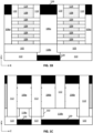
- spacer structures 110 are present along the sidewalls of gate structures 108. Spacer structures 110 may be any dielectric material, such as silicon nitride or silicon oxynitride, and provide separation between a given gate structure 108 and the adjacent source or drain region 106a/106b and contacts 116. Spacer structures 110 may run along sidewalls of gate structure 108 in the second direction and extend the entire height of gate structure 108 along the Z-axis. In this example, spacer structures 110 generally include both the upper spacers (sometimes called gate spacers, which may be formed during dummy or initial gate formation) and lower spacers (sometimes called inner gate spacers, which may be formed during source/drain processing).
- upper spacers sometimes called gate spacers, which may be formed during
- adjacent gate structures 108 may be separated from one another along the second direction (e.g., along the Y-axis) by a dielectric wall 112 (sometimes referred to as a gate cut).
- a dielectric wall 112 (sometimes referred to as a gate cut).
- Any number of suitable dielectric materials can be used for dielectric wall 112, such as silicon nitride or silicon oxynitride or low-k versions of these (e.g., porous silicon oxynitride).
- Any number of dielectric walls 112 may run lengthwise parallel to one another along the X-axis and may extend along the Z-axis at least through an entire thickness of one or more gate structures 108 and up to (or through) a cap layer 114 on a top surface of gate structures 108, as shown in this example.
- dielectric wall 112 continues to extend along the X-axis between multiple pairs of semiconductor devices and between the source or drain regions 106a/106b of the devices.
- Dielectric cap layer 114 may run lengthwise along the Y-axis along the top surface of gate structures 108 and be interrupted by dielectric wall 112. Cap layer 114 may include the same dielectric material as dielectric wall 112, in some examples.
- any number of frontside conductive contacts 116 are on corresponding source or drain regions 106a/106b. Adjacent frontside conductive contacts 116 may be separated by dielectric wall 112 or may connect together over or through dielectric wall 112 (e.g., via a bridging conductor). Frontside conductive contacts 116 can include any suitable conductive material, such as tungsten, ruthenium, cobalt, molybdenum, titanium, tantalum, or other metals or alloys thereof. Frontside conductive contacts 116 may be formed together such that they include the same conductive material.
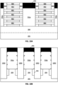
- backside source or drain regions 118a/118b are provided directly beneath the corresponding frontside source or drain regions 106a/106b.
- the dotted lines across both the X and Y directions are used to roughly differentiate between the frontside and backside source/drain regions.
- backside source or drain regions 118a/118b are grown from within recesses formed on the backside of the structure which expose the bottom surfaces of source or drain regions 106a/106b. Accordingly, a seam may be present between backside source or drain regions 118a/118b and frontside source or drain regions 106a/106b where two different epitaxial growth processes occur.
- Backside source or drain regions 118a/118b may have the same dopant type as their corresponding frontside source or drain regions 106a/106b.
- backside source or drain regions 118a/118b connect between adjacent source or drain regions 106a/106b, such as shown in the example structure of Figure 1A for backside source or drain region 118b, which connects two corresponding frontside source or drain regions 106b that were otherwise separated by dielectric wall 112.
- backside source or drain regions 118a/118b have a higher n-type or p-type dopant concentration compared to their corresponding frontside source or drain regions 106a/106b.
- a n-type frontside source or drain region 106a may have a dopant concentration between about 4 ⁇ 10 20 - 6 ⁇ 10 20 cm -3 while a n-type backside source or drain 118a region may have a dopant concentration between about 7 ⁇ 10 20 - 8 ⁇ 10 20 cm -3 ; and a p-type frontside source or drain region 106b may have a dopant concentration between about 2 ⁇ 10 21 - 3 ⁇ 10 21 cm -3 while a p-type backside source or drain region 118b may have a dopant concentration between about 3 ⁇ 10 21 - 4 ⁇ 10 21 cm -3 .
- Other doping schemes may be used as well.
- Backside source or drain regions 118a/118b may extend out and over a portion of the lower surface of base dielectric layer 102, thus increasing the contact area for the overall source or drain structure.
- one or more backside conductive contacts 120 are formed on the lower surface of backside source or drain regions 118a/118b.
- Backside conductive contacts 120 may include any of the same materials noted above for frontside conductive contacts 116.
- backside conductive contacts 120 and frontside conductive contacts 116 include the same conductive material.
- Backside conductive contacts 120 may connect to backside power or ground rails, or to a signal routing interconnect structure.
- backside conductive contacts 120 are formed through a backside dielectric layer 122.
- Backside dielectric layer 122 may represent any number of different dielectric layers and may include any suitable dielectric material, such as silicon dioxide. According to some embodiments, additional dielectric layers and conductive elements can be formed beneath backside dielectric layer 122 to create a backside interconnect structure (such as a power delivery network and/or signal routing network).
- a backside interconnect structure such as a power delivery network and/or signal routing network.
- backside source or drain regions 118a/118b do not extend below the bottom surface of base dielectric layer 102, but a taper of the sidewalls of the recess in which contacts 120 sit may be provisioned so as to provide an increase in the backside contact area for backside source or drain regions 118a/118b.
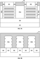
- Figures 2A - 14A and 2B - 14B include cross-sectional views that collectively illustrate an example process for forming an integrated circuit configured with backside source or drain regions, in accordance with an embodiment of the present disclosure.
- Figures 2A - 14A represent a similar cross-sectional view taken across the XZ plane in Figure 1A
- Figures 2B - 14B represent a cross-sectional view taken across the YZ in Figure 1A .
- FIG. 14A - 14B or Figures 14A' - 14B' ), which is similar to the structure shown in Figures 1B and 1C .
- Such a structure may be part of an overall integrated circuit (e.g., such as a processor or memory chip) that includes, for example, digital logic cells and/or memory cells and analog mixed signal circuitry.
- the illustrated integrated circuit structure may be part of a larger integrated circuit that includes other integrated circuitry not depicted.
- Example materials and process parameters are given, but the present disclosure is not intended to be limited to any specific such materials or parameters, as will be appreciated.
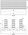
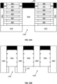
- Figures 2A and 2B each illustrates a cross-sectional view taken through a substrate 201 having a series of material layers formed over the substrate, according to an embodiment of the present disclosure.
- Alternating material layers may be deposited over a substrate 201 including sacrificial layers 202 alternating with semiconductor layers 204.
- the alternating layers are used to form GAA transistor structures. Any number of alternating sacrificial layers 202 and semiconductor layers 204 may be deposited over substrate 201.
- Substrate 201 can be, for example, a bulk substrate including group IV semiconductor material (such as silicon, germanium, or silicon germanium), group III-V semiconductor material (such as gallium arsenide, indium gallium arsenide, or indium phosphide), and/or any other suitable material upon which transistors can be formed.
- substrate 201 can be a semiconductor-on-insulator substrate having a desired semiconductor layer over a buried insulator layer (e.g., silicon over silicon dioxide).
- substrate 201 can be a multilayer substrate or superlattice suitable for forming nanowires or nanoribbons (e.g., alternating layers of silicon and SiGe, or alternating layers indium gallium arsenide and indium phosphide). Any number of substrates can be used.
- nanowires or nanoribbons e.g., alternating layers of silicon and SiGe, or alternating layers indium gallium arsenide and indium phosphide. Any number of substrates can be used.
- semiconductor layers 204 have a different material composition than sacrificial layers 202.
- semiconductor layers 204 are silicon germanium (SiGe) while sacrificial layers 202 include a semiconductor material suitable for use as a nanoribbon such as silicon (Si), SiGe, germanium, or III-V materials like indium phosphide (InP) or gallium arsenide (GaAs).
- SiGe silicon germanium
- germanium silicon germanium
- GaAs gallium arsenide
- the germanium concentration is different between semiconductor layers 204 and sacrificial layers 202.
- semiconductor layers 204 may include a higher germanium content compared to sacrificial layers 202.
- sacrificial layers 202 may be doped with either n-type dopants (to produce a p-channel transistor) or p-type dopants (to produce an n-channel transistor).
- the thickness of each semiconductor layer 204 may be between about 5 nm and about 20 nm. In some embodiments, the thickness of each semiconductor layer 204 is substantially the same (e.g., within 1-2 nm). The thickness of each of sacrificial layers 202 may be about the same as the thickness of each semiconductor layer 204 (e.g., about 5-20 nm). Each of semiconductor layers 204 and sacrificial layers 202 may be deposited using any known material deposition technique, such as chemical vapor deposition (CVD), plasma-enhanced chemical vapor deposition (PECVD), physical vapor deposition (PVD), or atomic layer deposition (ALD), or epitaxial growth.
- CVD chemical vapor deposition
- PECVD plasma-enhanced chemical vapor deposition
- PVD physical vapor deposition
- ALD atomic layer deposition
- FIGS 3A and 3B depict the cross-section views of the structure shown in Figures 2A and 2B , respectively, following the formation of a cap layer 302 and the subsequent formation of fins beneath cap layer 302, according to an embodiment.
- Cap layer 302 may be any suitable hard mask material such as a carbon hard mask (CHM) or silicon nitride.
- CHM carbon hard mask
- Cap layer 302 is patterned into rows to form corresponding rows of fins from the alternating layer stack of sacrificial layers 202 and semiconductor layers 204.
- Cap layer 302 extends along the top of each fin in a first direction, as seen in Figure 3A .
- an anisotropic etching process through the layer stack continues into at least a portion of substrate 201. Portions of substrate 201 beneath the fins are not etched and yield subfin regions 304.
- the etched portion of substrate 201 may be filled with a dielectric fill 306 that acts as shallow trench isolation (STI) between adjacent fins.
- Dielectric fill 306 may be any dielectric material such as silicon oxide.
- Subfin regions 304 represent remaining portions of substrate 201 between dielectric fill 306, according to some embodiments.
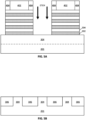
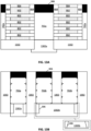
- FIGS 4A and 4B depict cross-section views of the structures shown in Figures 3A and 3B following the formation of sacrificial gates 402, according to some embodiments.
- a gate masking layer may first be patterned in strips that extend orthogonally across each of the fins (e.g., in a second direction) in order to form corresponding sacrificial gates 402 in strips beneath the gate masking layers. Afterwards, the gate masking layers may be removed or may remain as a cap layer above each sacrificial gate 402. According to some embodiments, the sacrificial gate material is removed in all areas not protected by the gate masking layers. Sacrificial gate 402 may be any material that can be selectively removed without damaging the semiconductor material of the fins. In some examples, sacrificial gate 402 includes polysilicon.
- spacer structures 404 are formed along the sidewalls of sacrificial gates 402. Spacer structures 404 may be deposited and then etched back such that spacer structures 404 remain mostly only on sidewalls of any exposed structures. In the cross-section view of Figure 4B , spacer structures 404 may also be formed along sidewalls of the exposed fins over dielectric fill 306. Such sidewall spacers on the fins can be removed during later processing when forming the source or drain regions, but as shown in this example may also remain in the final structure.
- spacer structures 404 may be any suitable dielectric material, such as silicon nitride, silicon carbon nitride, or silicon oxycarbonitride.
- spacer structures 404 comprise a nitride and dielectric fill 306 comprises an oxide, so as to provide a degree of etch selectivity during final gate processing.
- Other etch selective dielectric schemes e.g., oxide/carbide, carbide/nitride
- spacer structures 404 and dielectric fill 306 are compositionally the same or otherwise similar, where etch selectivity is not employed.
- Figures 5A and 5B depict cross-section views of the structures shown in Figures 4A and 4B following the removal of exposed portions of the fins not protected by sacrificial gates 402 and spacer structures 404, according to some embodiments.
- the exposed fin portions may be removed using any anisotropic etching process, such as reactive ion etching (RIE).
- RIE reactive ion etching
- the removal of the exposed fin portions creates source or drain trenches that alternate with gate trenches (currently filled with sacrificial gates 402) along the first direction, according to some embodiments.
- at least a portion of subfin regions 304 are also removed such that a top surface of subfin regions 304 is recessed below a top surface of dielectric fill 306.
- the recessed area above subfin regions 304 may be filled with one or more dielectric materials.
- the recessed area between dielectric fill 306 is replaced with a sacrificial material (such as aluminum oxide) that can be removed at a later time from the backside to expose the underside of source or drain regions.
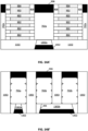
- Figures 6A and 6B depict cross-section views of the structures shown in Figures 5A and 5B following the removal of portions of sacrificial layers 202 and subsequent formation of internal spacers 602 (sometimes called lower gate spacers), according to an embodiment of the present disclosure.
- An isotropic etching process may be used to selectively recess the exposed ends of each sacrificial layer 202 (e.g., while etching comparatively little of semiconductor layers 204).
- Internal spacers 602 may have a material composition that is similar to or the exact same as spacer structures 404. Accordingly, internal spacers 602 may be any dielectric material that exhibits high etch selectively to semiconductor materials such as silicon and/or silicon germanium.
- Figures 7A and 7B depict cross-section views of the structure shown in Figures 6A and 6B , respectively, following the formation of source or drain regions 702a/702b within the source/drain trenches, according to some embodiments.
- Source or drain regions 702a/702b may be formed in the areas that had been previously occupied by the exposed fins between spacer structures 404.
- source or drain regions 702a/702b are epitaxially grown from the exposed semiconductor material at the ends of semiconductor layers 204.
- backside source or drain regions 1302a/1302b have a higher n-type or p-type dopant concentration compared to their corresponding source or drain regions 702a/702b.
- Figure 16 is a flow chart of a method 1600 for forming at least a portion of an integrated circuit, according to an embodiment.
- Various operations of method 1600 may be illustrated in Figures 2A - 14A and 2B - 14B .
- the correlation of the various operations of method 1600 to the specific components illustrated in the aforementioned figures is not intended to imply any structural and/or use limitations. Rather, the aforementioned figures provide one example embodiment of method 1600.
- Other operations may be performed before, during, or after any of the operations of method 1600.
- method 1600 does not explicitly describe various standard processes that are usually performed to form transistor structures. Some of the operations of method 1600 may be performed in a different order than the illustrated order.
- Method 1600 begins with operation 1602 where a plurality of parallel semiconductor fins are formed, according to some embodiments.
- the semiconductor material in the fins may be formed from a substrate such that the fins are an integral part of the substrate (e.g., etched from a bulk silicon substrate).
- the fins can be formed of material deposited onto an underlying substrate.
- a blanket layer of silicon germanium (SiGe) can be deposited onto a silicon substrate, and then patterned and etched to form a plurality of SiGe fins extending from that substrate.
- non-native fins can be formed in a so-called aspect ratio trapping based process, where native fins are etched away so as to leave fin-shaped trenches which can then be filled with an alternative semiconductor material (e.g., group IV or III-V material).
- the fins include alternating layers of material (e.g., alternating layers of silicon and SiGe) that facilitates forming of nanowires and nanoribbons during a gate forming process where one type of the alternating layers are selectively etched away so as to liberate the other type of alternating layers within the channel region, so that a gate-all-around (GAA) process can then be carried out.
- GAA gate-all-around
- Method 1602 continues with operation 1604 where a dielectric layer is formed around subfin portions of the one or more fins.
- the dielectric layer extends between each pair of adjacent parallel fins and runs lengthwise in the same direction as the fins.
- the anisotropic etching process that forms the fins also etches into a portion of the substrate and the dielectric layer may be formed within the recessed portions of the substrate. Accordingly, the dielectric layer acts as shallow trench isolation (STI) between adjacent fins.
- the dielectric layer may be any suitable dielectric material, such as silicon dioxide.
- Method 1600 continues with operation 1612 where the substrate is removed from the backside of the structure to expose the bottom surface of the subfin portions and/or the bottom surface of the dielectric layer adjacent to the subfin portions.
- the substrate may be removed using any number of isotropic etching, polishing, or grinding operations.
- the subfin portions may also be removed and replaced with any suitable dielectric material(s), such as silicon dioxide.
- Method 1600 continues with operation 1614 where a recess is formed through the dielectric material(s) on the backside to expose the bottom surface of a first source or drain region.
- the first source or drain region may be any n-type or p-type source or drain region and may represent more than one adjacent source or drain region.
- the recess may be formed using any suitable anisotropic etching technique, such as RIE. According to some embodiments, the recess may have sidewalls that taper inwards towards the exposed surface of the first source or drain.
- Method 1600 continues with operation 1616 where a second source or drain region is formed within the recess and on a bottom surface of the first source or drain region.
- the second source or drain region may be epitaxially grown from the exposed bottom surface of the first source or drain region. Since a new epitaxial growth process is performed to create the second source or drain region, a seam or noticeable difference in grain structure may be present at the boundary between the first source or drain region and the second source or drain region. In some examples, the second source or drain region may grow across two or more source or drain regions.
- the second source or drain region expands the available contact area beyond what was available for the first source or drain region.
- the second source or drain region grows beyond the bottom surface of the dielectric layer (out of the recess) to create more contact surface area on the exposed bottom surface of the second source or drain region.
- the second source or drain region remains within the backside recess, but the contact surface area is still expanded due to the inward taper of the backside recess sidewalls.
- the second source or drain region has a higher n-type or p-type dopant concentration compared to the first source or drain region.
- Method 1600 continues with operation 1618 where a backside contact is formed on any exposed surface of the second source or drain region.
- the backside contact may include any suitable conductive material, such as cobalt, ruthenium, molybdenum, or tungsten.
- the backside contact is part of a backside interconnect structure to connect the second source or drain region and the first source or drain region to a power or ground rail.
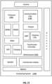
- computing system 1700 may include one or more other components that may or may not be physically and electrically coupled to the motherboard 1702. These other components may include, but are not limited to, volatile memory (e.g., DRAM), non-volatile memory (e.g., ROM), a graphics processor, a digital signal processor, a crypto processor, a chipset, an antenna, a display, a touchscreen display, a touchscreen controller, a battery, an audio codec, a video codec, a power amplifier, a global positioning system (GPS) device, a compass, an accelerometer, a gyroscope, a speaker, a camera, and a mass storage device (such as hard disk drive, compact disk (CD), digital versatile disk (DVD), and so forth).
- volatile memory e.g., DRAM
- non-volatile memory e.g., ROM
- graphics processor e.g., a digital signal processor
- crypto processor e.g., a graphics processor
- any of the components included in computing system 1700 may include one or more integrated circuit structures or devices configured in accordance with an example embodiment (e.g., a module including one or more semiconductor devices that include a backside source or drain region on a frontside source or drain region to improve backside contact area, as variously provided herein).
- a module including one or more semiconductor devices that include a backside source or drain region on a frontside source or drain region to improve backside contact area as variously provided herein.
- multiple functions can be integrated into one or more chips (e.g., for instance, note that the communication chip 1706 can be part of or otherwise integrated into the processor 1704).
- the communication chip 1706 enables wireless communications for the transfer of data to and from the computing system 1700.
- wireless and its derivatives may be used to describe circuits, devices, systems, methods, techniques, communications channels, etc., that may communicate data through the use of modulated electromagnetic radiation through a non-solid medium. The term does not imply that the associated devices do not contain any wires, although in some embodiments they might not.
- the communication chip 1706 may implement any of a number of wireless standards or protocols, including, but not limited to, Wi-Fi (IEEE 802.11 family), WiMAX (IEEE 802.16 family), IEEE 802.20, long term evolution (LTE), Ev-DO, HSPA+, HSDPA+, HSUPA+, EDGE, GSM, GPRS, CDMA, TDMA, DECT, Bluetooth, derivatives thereof, as well as any other wireless protocols that are designated as 3G, 4G, 5G, and beyond.
- the computing system 1700 may include a plurality of communication chips 1706.
- a first communication chip 1706 may be dedicated to shorter range wireless communications such as Wi-Fi and Bluetooth and a second communication chip 1706 may be dedicated to longer range wireless communications such as GPS, EDGE, GPRS, CDMA, WiMAX, LTE, Ev-DO, and others.
- the processor 1704 of the computing system 1700 includes an integrated circuit die packaged within the processor 1704.
- the integrated circuit die of the processor includes onboard circuitry that is implemented with one or more semiconductor devices as variously described herein.
- the term "processor" may refer to any device or portion of a device that processes, for instance, electronic data from registers and/or memory to transform that electronic data into other electronic data that may be stored in registers and/or memory.
- the communication chip 1706 also may include an integrated circuit die packaged within the communication chip 1706.
- the integrated circuit die of the communication chip includes one or more semiconductor devices as variously described herein.
- multi-standard wireless capability may be integrated directly into the processor 1704 (e.g., where functionality of any chips 1706 is integrated into processor 1704, rather than having separate communication chips).
- processor 1704 may be a chip set having such wireless capability.
- any number of processor 1704 and/or communication chips 1706 can be used.
- any one chip or chip set can have multiple functions integrated therein.
- the computing system 1700 may be a laptop, a netbook, a notebook, a smartphone, a tablet, a personal digital assistant (PDA), an ultra-mobile PC, a mobile phone, a desktop computer, a server, a printer, a scanner, a monitor, a set-top box, an entertainment control unit, a digital camera, a portable music player, a digital video recorder, or any other electronic device that processes data or employs one or more integrated circuit structures or devices formed using the disclosed techniques, as variously described herein.
- PDA personal digital assistant
- the various components of the computing system 1700 may be combined or integrated in a system-on-a-chip (SoC) architecture.
- the components may be hardware components, firmware components, software components or any suitable combination of hardware, firmware or software.
- Example 1 is an integrated circuit that includes one or more semiconductor bodies extending in a first direction from a first source or drain region, a gate structure extending over the one or more semiconductor bodies in a second direction different from the first direction, a dielectric layer beneath the gate structure, and a second source or drain region contacting a bottom surface of the first source or drain region, such that a seam is present between the first source or drain region and the second source or drain region.
- the second source or drain region contacts a sidewall of the dielectric layer.
- Example 2 includes the integrated circuit of Example 1, wherein the one or more semiconductor bodies are nanoribbons, nanosheets, or nanowires that comprise germanium, silicon, or any combination thereof.
- Example 3 includes the integrated circuit of Example 1 or 2, wherein the first source or drain region and the second source or drain region are both n-type regions or both p-type regions.
- Example 4 includes the integrated circuit of any one of Examples 1-3, further comprising a topside contact on a top surface of the first source or drain region such that the topside contact does not contact any portion of the second source or drain region.
- Example 5 includes the integrated circuit of any one of Examples 1-4, further comprising a backside contact on a bottom surface of the second source or drain region such that the backside contact does not contact any portion of the first source or drain region.
- Example 12 includes the integrated circuit of any one of Examples 1-11, wherein the one or more semiconductor bodies are one or more first semiconductor bodies, and the integrated circuit further comprises one or more second semiconductor bodies extending in the first direction from a third source or drain region adjacent to the first source or drain region along the second direction, wherein the second source or drain region further extends from a bottom of the third source or drain region.
- Example 19 includes the electronic device of Example 17 or 18, wherein the first source or drain region and the second source or drain region are both n-type regions or both p-type regions.
- Example 26 includes the electronic device of any one of Examples 17-25, wherein the first direction is orthogonal to the second direction.
- Example 29 includes the electronic device of any one of Examples 17-28, further comprising a printed circuit board, wherein the chip package is attached to the printed circuit board.
- Example 45 includes the integrated circuit of any one of Examples 37-44, wherein the second source or drain region extends below a bottom surface of the dielectric layer.
- Example 46 includes the integrated circuit of any one of Examples 37-45, wherein the first direction is orthogonal to the second direction.
- Example 49 is a printed circuit board that includes the integrated circuit of any one of Examples 37-48.
- Example 50 is an integrated circuit that includes one or more semiconductor bodies extending in a first direction from a first source or drain region, a gate structure extending over the one or more semiconductor bodies in a second direction different from the first direction, a dielectric layer beneath the gate structure, and a second source or drain region extending from a bottom of the first source or drain region.
- the second source or drain region is at least partially laterally between first and second portions of the dielectric layer.
- the first source or drain region is fully above the dielectric layer.
- Example 52 includes the integrated circuit of Example 50 or 51, wherein the first source or drain region and the second source or drain region are both n-type regions or both p-type regions.
- Example 53 includes the integrated circuit of any one of Examples 50-52, further comprising a topside contact on a top surface of the first source or drain region such that the topside contact does not contact any portion of the second source or drain region.
- Example 54 includes the integrated circuit of any one of Examples 50-53, further comprising a backside contact on a bottom surface of the second source or drain region such that the backside contact does not contact any portion of the first source or drain region.
- Example 55 includes the integrated circuit of Example 54, wherein the backside contact comprises any one of tungsten, ruthenium, molybdenum, or cobalt.
- Example 56 includes the integrated circuit of Example 54 or 55, wherein the backside contact also contacts the sidewall of the dielectric layer.
- Example 57 includes the integrated circuit of Example 56, wherein the sidewall of the dielectric layer is tapered, such that the second source or drain region is also tapered and gets wider as it extends away from the first source or drain region.
- Example 58 includes the integrated circuit of Example 56 or 57, wherein the sidewall of the dielectric layer is tapered, such that the backside contact is also tapered and gets wider as it extends away from the second source or drain region.
- Example 59 includes the integrated circuit of any one of Examples 54-57, wherein the backside contact is fully beneath the dielectric layer.
- Example 60 includes the integrated circuit of any one of Examples 50-59, wherein the second source or drain region extends below a bottom surface of the dielectric layer.
- Example 61 includes the integrated circuit of any one of Examples 50-60, wherein the first direction is orthogonal to the second direction.
- Example 62 includes the integrated circuit of any one of Examples 50-61, wherein the one or more semiconductor bodies are one or more first semiconductor bodies, and the integrated circuit further comprises one or more second semiconductor bodies extending in the first direction from a third source or drain region adjacent to the first source or drain region along the second direction, wherein the second source or drain region further contacts a bottom surface of the third source or drain region and the second source or drain region has a higher n-type dopant concentration or a higher p-type dopant concentration compared to the third source or drain region.
- Example 63 includes the integrated circuit of any one of Examples 50-62, wherein a seam is present between the first source or drain region and the second source or drain region.
- Example 64 is a printed circuit board that includes the integrated circuit of any one of Examples 50-63.
Landscapes
- Insulated Gate Type Field-Effect Transistor (AREA)
Applications Claiming Priority (1)
| Application Number | Priority Date | Filing Date | Title |
|---|---|---|---|
| US18/400,310 US20250220994A1 (en) | 2023-12-29 | 2023-12-29 | Backside epitaxial growth for improved contact area |
Publications (1)
| Publication Number | Publication Date |
|---|---|
| EP4580333A1 true EP4580333A1 (de) | 2025-07-02 |
Family
ID=93460645
Family Applications (1)
| Application Number | Title | Priority Date | Filing Date |
|---|---|---|---|
| EP24211792.7A Pending EP4580333A1 (de) | 2023-12-29 | 2024-11-08 | Rückseitiges epitaxialwachstum für verbesserte kontaktfläche |
Country Status (2)
| Country | Link |
|---|---|
| US (1) | US20250220994A1 (de) |
| EP (1) | EP4580333A1 (de) |
Families Citing this family (1)
| Publication number | Priority date | Publication date | Assignee | Title |
|---|---|---|---|---|
| US20230402507A1 (en) * | 2022-06-13 | 2023-12-14 | Intel Corporation | Dual metal silicide for stacked transistor devices |
Citations (3)
| Publication number | Priority date | Publication date | Assignee | Title |
|---|---|---|---|---|
| US20210074823A1 (en) * | 2016-09-30 | 2021-03-11 | Intel Corporation | Backside source/drain replacement for semiconductor devices with metallization on both sides |
| US20210399099A1 (en) * | 2020-06-17 | 2021-12-23 | Taiwan Semiconductor Manufacturing Co., Ltd. | Epitaxial backside contact |
| US20230317782A1 (en) * | 2022-03-29 | 2023-10-05 | International Business Machines Corporation | Self-aligned backside trench epitaxy for low contact resistivity |
-
2023
- 2023-12-29 US US18/400,310 patent/US20250220994A1/en active Pending
-
2024
- 2024-11-08 EP EP24211792.7A patent/EP4580333A1/de active Pending
Patent Citations (3)
| Publication number | Priority date | Publication date | Assignee | Title |
|---|---|---|---|---|
| US20210074823A1 (en) * | 2016-09-30 | 2021-03-11 | Intel Corporation | Backside source/drain replacement for semiconductor devices with metallization on both sides |
| US20210399099A1 (en) * | 2020-06-17 | 2021-12-23 | Taiwan Semiconductor Manufacturing Co., Ltd. | Epitaxial backside contact |
| US20230317782A1 (en) * | 2022-03-29 | 2023-10-05 | International Business Machines Corporation | Self-aligned backside trench epitaxy for low contact resistivity |
Also Published As
| Publication number | Publication date |
|---|---|
| US20250220994A1 (en) | 2025-07-03 |
Similar Documents
| Publication | Publication Date | Title |
|---|---|---|
| US20240321737A1 (en) | Isolated backside contacts for semiconductor devices | |
| EP4580333A1 (de) | Rückseitiges epitaxialwachstum für verbesserte kontaktfläche | |
| US20250311353A1 (en) | Dielectric wall used to separate gate dielectric between adjacent devices | |
| EP4435841A1 (de) | Über einen angrenzenden source- oder drainbereich erweiterter kontakt | |
| EP4485514A1 (de) | Durchgangsstrukturen mit niedrigem widerstand | |
| US20240321872A1 (en) | Gate link across gate cut in semiconductor devices | |
| US20240203739A1 (en) | Dielectric layer stack for wide gate cut structures | |
| US12490462B2 (en) | Angled gate or diffusion plugs | |
| EP4626168A1 (de) | Gate-all-around-transistor ohne hohlraumabstandsstrukturen | |
| US20250204008A1 (en) | Conductive interconnect structure within gate cut | |
| US20260032960A1 (en) | Backside contact structure with enhanced ohmic contact | |
| US12563810B1 (en) | Selective backside recessing of source and drain regions | |
| EP4625483A2 (de) | Leitfähige durchkontaktierung durch eine rippenisolationsstruktur zwischen halbleiterbauelementen | |
| US20240355915A1 (en) | Backside conductive structures extending through integrated circuit to meet frontside contacts | |
| EP4576087A1 (de) | Rückseiten-logikverbindungen | |
| US20240321685A1 (en) | Semiconductor devices between gate cuts and deep backside vias | |
| US20250072069A1 (en) | Recessed via with conductive link to adjacent contact | |
| US20260006859A1 (en) | Strain engineering using gate cuts | |
| EP4246564A1 (de) | Partielle gate-cut-strukturen in einer integrierten schaltung | |
| EP4709082A1 (de) | Selbstjustierter gate-schnitt mit hybrider architektur | |
| US20250380494A1 (en) | Subfin engineering to improve semiconductor device performance | |
| US20240321738A1 (en) | Bridging contact structures | |
| US20250294866A1 (en) | Gate cut confined within gate trench | |
| US20250372384A1 (en) | Self-aligned gate cut | |
| EP4693289A1 (de) | Gestapelte halbleiterbauelemente mit gekoppelten rückseitenkontakten |
Legal Events
| Date | Code | Title | Description |
|---|---|---|---|
| PUAI | Public reference made under article 153(3) epc to a published international application that has entered the european phase |
Free format text: ORIGINAL CODE: 0009012 |
|
| STAA | Information on the status of an ep patent application or granted ep patent |
Free format text: STATUS: THE APPLICATION HAS BEEN PUBLISHED |
|
| AK | Designated contracting states |
Kind code of ref document: A1 Designated state(s): AL AT BE BG CH CY CZ DE DK EE ES FI FR GB GR HR HU IE IS IT LI LT LU LV MC ME MK MT NL NO PL PT RO RS SE SI SK SM TR |
|
| STAA | Information on the status of an ep patent application or granted ep patent |
Free format text: STATUS: REQUEST FOR EXAMINATION WAS MADE |
|
| 17P | Request for examination filed |
Effective date: 20260102 |