EP4199043A1 - Method for manufacturing semiconductor structure - Google Patents
Method for manufacturing semiconductor structure Download PDFInfo
- Publication number
- EP4199043A1 EP4199043A1 EP21934380.3A EP21934380A EP4199043A1 EP 4199043 A1 EP4199043 A1 EP 4199043A1 EP 21934380 A EP21934380 A EP 21934380A EP 4199043 A1 EP4199043 A1 EP 4199043A1
- Authority
- EP
- European Patent Office
- Prior art keywords
- layer
- region
- top surface
- trench
- opening
- Prior art date
- Legal status (The legal status is an assumption and is not a legal conclusion. Google has not performed a legal analysis and makes no representation as to the accuracy of the status listed.)
- Pending
Links
- 238000000034 method Methods 0.000 title claims abstract description 48
- 239000004065 semiconductor Substances 0.000 title claims abstract description 18
- 238000004519 manufacturing process Methods 0.000 title claims abstract description 17
- 238000002955 isolation Methods 0.000 claims abstract description 49
- 238000005530 etching Methods 0.000 claims abstract description 43
- 239000000758 substrate Substances 0.000 claims abstract description 26
- 238000001312 dry etching Methods 0.000 claims abstract description 13
- 239000000463 material Substances 0.000 claims description 44
- 229920002120 photoresistant polymer Polymers 0.000 claims description 26
- OKTJSMMVPCPJKN-UHFFFAOYSA-N Carbon Chemical compound [C] OKTJSMMVPCPJKN-UHFFFAOYSA-N 0.000 claims description 6
- 229910052799 carbon Inorganic materials 0.000 claims description 6
- 230000002093 peripheral effect Effects 0.000 claims description 4
- 238000004528 spin coating Methods 0.000 claims description 3
- 150000001875 compounds Chemical class 0.000 claims 1
- 238000011049 filling Methods 0.000 abstract description 10
- 239000010410 layer Substances 0.000 description 397
- 239000011241 protective layer Substances 0.000 description 14
- 230000007423 decrease Effects 0.000 description 10
- 238000000151 deposition Methods 0.000 description 7
- 230000008021 deposition Effects 0.000 description 6
- 230000015572 biosynthetic process Effects 0.000 description 5
- 238000005137 deposition process Methods 0.000 description 5
- 238000010586 diagram Methods 0.000 description 4
- 239000003795 chemical substances by application Substances 0.000 description 3
- VYPSYNLAJGMNEJ-UHFFFAOYSA-N Silicium dioxide Chemical compound O=[Si]=O VYPSYNLAJGMNEJ-UHFFFAOYSA-N 0.000 description 2
- 230000008901 benefit Effects 0.000 description 2
- 230000000295 complement effect Effects 0.000 description 2
- 230000000694 effects Effects 0.000 description 2
- 238000012986 modification Methods 0.000 description 2
- 230000004048 modification Effects 0.000 description 2
- 238000004904 shortening Methods 0.000 description 2
- 239000000126 substance Substances 0.000 description 2
- XUIMIQQOPSSXEZ-UHFFFAOYSA-N Silicon Chemical compound [Si] XUIMIQQOPSSXEZ-UHFFFAOYSA-N 0.000 description 1
- 239000002131 composite material Substances 0.000 description 1
- 238000011068 loading method Methods 0.000 description 1
- 229910052710 silicon Inorganic materials 0.000 description 1
- 239000010703 silicon Substances 0.000 description 1
- 235000012239 silicon dioxide Nutrition 0.000 description 1
- 239000000377 silicon dioxide Substances 0.000 description 1
Images


Classifications
-
- H—ELECTRICITY
- H01—ELECTRIC ELEMENTS
- H01L—SEMICONDUCTOR DEVICES NOT COVERED BY CLASS H10
- H01L21/00—Processes or apparatus adapted for the manufacture or treatment of semiconductor or solid state devices or of parts thereof
- H01L21/02—Manufacture or treatment of semiconductor devices or of parts thereof
- H01L21/04—Manufacture or treatment of semiconductor devices or of parts thereof the devices having potential barriers, e.g. a PN junction, depletion layer or carrier concentration layer
- H01L21/18—Manufacture or treatment of semiconductor devices or of parts thereof the devices having potential barriers, e.g. a PN junction, depletion layer or carrier concentration layer the devices having semiconductor bodies comprising elements of Group IV of the Periodic Table or AIIIBV compounds with or without impurities, e.g. doping materials
- H01L21/30—Treatment of semiconductor bodies using processes or apparatus not provided for in groups H01L21/20 - H01L21/26
- H01L21/302—Treatment of semiconductor bodies using processes or apparatus not provided for in groups H01L21/20 - H01L21/26 to change their surface-physical characteristics or shape, e.g. etching, polishing, cutting
- H01L21/306—Chemical or electrical treatment, e.g. electrolytic etching
- H01L21/308—Chemical or electrical treatment, e.g. electrolytic etching using masks
- H01L21/3083—Chemical or electrical treatment, e.g. electrolytic etching using masks characterised by their size, orientation, disposition, behaviour, shape, in horizontal or vertical plane
- H01L21/3086—Chemical or electrical treatment, e.g. electrolytic etching using masks characterised by their size, orientation, disposition, behaviour, shape, in horizontal or vertical plane characterised by the process involved to create the mask, e.g. lift-off masks, sidewalls, or to modify the mask, e.g. pre-treatment, post-treatment
-
- H—ELECTRICITY
- H01—ELECTRIC ELEMENTS
- H01L—SEMICONDUCTOR DEVICES NOT COVERED BY CLASS H10
- H01L21/00—Processes or apparatus adapted for the manufacture or treatment of semiconductor or solid state devices or of parts thereof
- H01L21/02—Manufacture or treatment of semiconductor devices or of parts thereof
- H01L21/027—Making masks on semiconductor bodies for further photolithographic processing not provided for in group H01L21/18 or H01L21/34
- H01L21/033—Making masks on semiconductor bodies for further photolithographic processing not provided for in group H01L21/18 or H01L21/34 comprising inorganic layers
- H01L21/0334—Making masks on semiconductor bodies for further photolithographic processing not provided for in group H01L21/18 or H01L21/34 comprising inorganic layers characterised by their size, orientation, disposition, behaviour, shape, in horizontal or vertical plane
- H01L21/0337—Making masks on semiconductor bodies for further photolithographic processing not provided for in group H01L21/18 or H01L21/34 comprising inorganic layers characterised by their size, orientation, disposition, behaviour, shape, in horizontal or vertical plane characterised by the process involved to create the mask, e.g. lift-off masks, sidewalls, or to modify the mask, e.g. pre-treatment, post-treatment
-
- H—ELECTRICITY
- H01—ELECTRIC ELEMENTS
- H01L—SEMICONDUCTOR DEVICES NOT COVERED BY CLASS H10
- H01L21/00—Processes or apparatus adapted for the manufacture or treatment of semiconductor or solid state devices or of parts thereof
- H01L21/02—Manufacture or treatment of semiconductor devices or of parts thereof
- H01L21/04—Manufacture or treatment of semiconductor devices or of parts thereof the devices having potential barriers, e.g. a PN junction, depletion layer or carrier concentration layer
- H01L21/18—Manufacture or treatment of semiconductor devices or of parts thereof the devices having potential barriers, e.g. a PN junction, depletion layer or carrier concentration layer the devices having semiconductor bodies comprising elements of Group IV of the Periodic Table or AIIIBV compounds with or without impurities, e.g. doping materials
- H01L21/30—Treatment of semiconductor bodies using processes or apparatus not provided for in groups H01L21/20 - H01L21/26
- H01L21/31—Treatment of semiconductor bodies using processes or apparatus not provided for in groups H01L21/20 - H01L21/26 to form insulating layers thereon, e.g. for masking or by using photolithographic techniques; After treatment of these layers; Selection of materials for these layers
- H01L21/3105—After-treatment
- H01L21/311—Etching the insulating layers by chemical or physical means
- H01L21/31105—Etching inorganic layers
- H01L21/31111—Etching inorganic layers by chemical means
- H01L21/31116—Etching inorganic layers by chemical means by dry-etching
-
- H—ELECTRICITY
- H01—ELECTRIC ELEMENTS
- H01L—SEMICONDUCTOR DEVICES NOT COVERED BY CLASS H10
- H01L21/00—Processes or apparatus adapted for the manufacture or treatment of semiconductor or solid state devices or of parts thereof
- H01L21/02—Manufacture or treatment of semiconductor devices or of parts thereof
- H01L21/04—Manufacture or treatment of semiconductor devices or of parts thereof the devices having potential barriers, e.g. a PN junction, depletion layer or carrier concentration layer
- H01L21/18—Manufacture or treatment of semiconductor devices or of parts thereof the devices having potential barriers, e.g. a PN junction, depletion layer or carrier concentration layer the devices having semiconductor bodies comprising elements of Group IV of the Periodic Table or AIIIBV compounds with or without impurities, e.g. doping materials
- H01L21/30—Treatment of semiconductor bodies using processes or apparatus not provided for in groups H01L21/20 - H01L21/26
- H01L21/31—Treatment of semiconductor bodies using processes or apparatus not provided for in groups H01L21/20 - H01L21/26 to form insulating layers thereon, e.g. for masking or by using photolithographic techniques; After treatment of these layers; Selection of materials for these layers
- H01L21/3105—After-treatment
- H01L21/311—Etching the insulating layers by chemical or physical means
- H01L21/31144—Etching the insulating layers by chemical or physical means using masks
Definitions
- the present application relates to the field of semiconductors, and in particular to a method for manufacturing a semiconductor structure.
- the mask layer may be either a photoresist layer or a mask layer composed of one or more other materials.
- the opening pattern may be formed either by exposing and developing photoresist, or by etching particular materials in a composite layer which are generally formed in a particular position in advance and occupy the position of a to-be-formed opening pattern.
- the etching of a to-be-etched region may be affected by adjacent regions. For example, a particular material is covered and cannot be exposed to the etching agent such that a preset opening pattern cannot be formed, thereby subjecting the target layer to incomplete selective etching.
- the embodiment of the application provides a method of manufacturing a semiconductor structure, whereby selective etching can be performed completely to the target layer.
- the embodiment of the application provides a method of manufacturing a semiconductor structure, which comprises the following steps: providing a substrate, comprising a first region, a second region, and a third region, wherein the second region is disposed between the first region and the third region; forming a target layer, a first mask layer, an isolation layer and an intermediate layer sequentially on the substrate, wherein the intermediate layer in the first region has at least one first trench therein which exposes the isolation layer, and the bottom and the sidewall of the first trench are covered with a sacrificial layer; etching a portion of the intermediate layer in the second region to form at least one second trench which is disposed in the intermediate layer in the second region; forming a fill layer which fills the first trench and the second trench, wherein the top surface of the fill layer is higher than the top surface of the intermediate layer, and the height difference between the top surface of the fill layer in the first region and the top surface of the fill layer in the second region is smaller than or equal to a first preset value in the direction
- the second trench is formed in the second region such that a portion of the fill layer material in the second region falls into the second trench, thereby reducing the height difference between the top surface of the fill layer in the first region and the top surface of the fill layer in the second region, avoiding a collapse of the fill layer in the second region whereby a portion of the material will slide to the top of the first region and enabling all the top surface of the sacrificial layer to be exposed without over-etching in the subsequent maskless dry etching process. Therefore, a complete first opening is formed and selective etching is performed completely to the target layer.
- the second opening and the third opening are formed, which prevents the photoresist layer used to form the second opening and the third opening from filling the first opening, thereby avoiding the trouble in removing the photoresist material which falls into the first opening and ensuring the effective execution of the subsequent etching process.
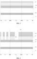
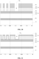
- FIGS. 1 to 18 are schematic structure diagrams corresponding to each step in a method of manufacturing a semiconductor structure. The method thereof comprises the following steps:
- a substrate 11 comprising a first region 111, a second region 112 and a third region 113, wherein the second region 112 is disposed between the first region 111 and the third region 113; and a target layer 121, a protective layer 13, an initial mask layer 141 and an initial intermediate layer 15 are formed on the substrate 11, which are stacked in sequence.
- a first photoresist layer 161 having a first opening pattern is formed on the initial intermediate layer 15; and the initial intermediate layer 15 is etched with the first opening pattern to form an intermediate trench 15a which exposes the surface of the initial mask layer 141.
- the arrangement density of the intermediate trenches 15a in the first region 111 is higher than the arrangement density of the intermediate trenches 15a in the second region 112, and the arrangement density of the intermediate trenches 15a in the second region 112 is higher than the arrangement density of the intermediate trenches 15a in the third region 113.
- an initial sacrificial layer 171 covering the bottom and the sidewall of the intermediate trench 15a, and the initial sacrificial layer 171 also covers the tops of the initial intermediate layers 15 in the first region 111, the second region 112 and the third region 113.
- a deposition process is performed to form an initial fill layer 181 filling the intermediate trench 15a.
- the deposition rates and the deposition time in different regions are the same. That is, the total material of the initial fill layer 181 deposited per unit area in any region is the same. Since the arrangement density of the intermediate trenches 15a in the first region 111, the second region 112 and the third region 113 decreases gradually, the first region 111 comprises the most number of intermediate trenches 15a per unit area and the second region 112 comprises the second most number of intermediate trenches 15a per unit area. The more intermediate trenches 15a there are, the more the material of the initial fill layer 181 can be accommodated, the less redundant material of the initial fill layer 181 there will be left on the initial intermediate layer 15 and the lower the top surface of the initial fill layer 181 will be. Accordingly, the top surface of the initial fill layer 181 in the first region 111, the second region 112 and the third region 113 rises gradually.
- the initial fill layer 181 is etched and the remaining initial fill layer 181 exposes the top surface of the initial sacrificial layer 171 which covers the sidewall of the intermediate trench 15a; and the initial sacrificial layer 171 covering the sidewall of the intermediate trench 15a is etched to form an initial gap 15b which exposes the surface of the initial mask layer 141.
- an initial gap 15b need not be formed in the third region 113. Accordingly, there is no intermediate trench 15a and initial sacrificial layer 171 in the initial intermediate layer 15 in the third region 113, and the initial fill layer 181 in the third region 113 need not be removed.
- the initial mask layer 141 is etched through the initial gap 15b to form a first mask layer 142; and the remaining initial intermediate layer 15, the remaining initial sacrificial layer 171 and the remaining initial fill layer 181 are removed after the first mask layer 142 is formed.
- the first mask layer 142 has a plurality of fourth openings 142a with the same opening width in a direction parallel to the substrate 11, wherein the width of the fourth opening 142a is equal to the thickness of the initial sacrificial layer 171 which covers the sidewall of the intermediate trench 15a; in addition, since the arrangement density of the intermediate trenches 15a in the first region 111, the second region 112 and the third region 113 decreases gradually, the arrangement density of the initial gaps 15b in the first region 111, the second region 112 and the third region 113 decreases gradually, and the arrangement density of the fourth openings 142a in the first region 111, the second region 112 and the third region 113 decreases gradually.
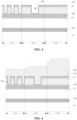
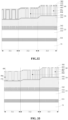
- the first mask layer 142 there is formed on the first mask layer 142 an isolation layer 19 and an intermediate layer 20 stacked in sequence.
- the top surface of the isolation layer 19 in the first region 111, the second region 112 and the third region 113 gradually rises when the isolation layer 19 and the intermediate layer 20 are uniformly deposited in different regions. Accordingly, the top surface of the intermediate layer 20 in the first region 111, the second region 112 and the third region 113 gradually rises.
- the intermediate layer 20 in the first region 111 there is formed in the intermediate layer 20 in the first region 111 at least one first trench 20a, which exposes the surface of the isolation layer 19; and there is formed a first sacrificial layer 172 which covers the bottom and the sidewall of the first trench 20a and the top surface of the intermediate layer 20 in the first region 111, the second region 112 and the third region 113.
- a second photoresist layer 162 is formed which fills the first trench 20a and is disposed on the intermediate layer 20 in the first region 111, the second region 112, and the third region 113.
- the second photoresist layer 162 has a second opening pattern disposed in the third region 113.
- the first sacrificial layer 172 and the intermediate layer 20 are etched with the second opening pattern to form a third trench 20C which is disposed in the intermediate layer 20 in the third region 113; and the second photoresist layer is removed after the third trench 20C is formed.
- a fill layer 182 is formed which fills the first trench 20a and the third trench 20c, and the upper surface of the fill layer 182 is higher than the upper surface of the intermediate layer 20.
- the total material of the fill layer 182 deposited per unit area in any region is the same.
- the top surface positions of the fill layer 182 in the different regions depend on two factors: one is the top surface position of the intermediate layer 20 in a region and the other is the arrangement density and the opening width of the trenches or the openings in the intermediate layer 20 in a region. The higher the top surface of the intermediate layer 20 is, the higher the top surface of the fill layer 182 is. Whereas the higher the arrangement density and the opening width of the trenches or openings in the intermediate layer 20 is, the lower the top surface of the fill layer 182 is.
- the top surface of the intermediate layer 20 in the first region 111 is lower than the top surface of the intermediate layer 20 in the second region 112, and the intermediate layer 20 in the first region 111 has the first trench 20a therein while the intermediate layer 20 in the second region 112 does not have a trench or an opening therein. Accordingly, the top surface of the fill layer 182 in the first region 111 is lower than the top surface of the fill layer 182 in the second region 112.
- the fill layer 182 on the intermediate layer 20 in the first edge region 111a is thicker, whereas the fill layer 182 on the intermediate layer 20 in the first central region 111b is thinner.
- the fill layer 182 is formed using a spin-coating process, the whole structure of the fill layer 182 will be loose and the strength of the structure will be low, thereby making the layer prone to collapse for lack of support. Accordingly, if the material of the fill layer 182 is carbon or a carbon-containing organic substance, the fill layer 182 which will have a softer texture, lower hardness and lower structure strength is also prone to collapse for lack of support.
- the intermediate layer 20 in the third region 113 has the third trenches 20C therein such that the top surface of the fill layer 182 in the third region 113 may be higher or lower than or flush with the top surface of the fill layer 182 in the second region 112 as the third trenches 20C vary in arrangement density and opening width.
- a portion of the fill layer 182 material in the third region 113 may collapse for lack of support and may slide to the second region 112 or even the first region 111, such that the top surface of the fill layer 182 in the first edge region 111a is higher; and when the top surface of the fill layer 182 in the third region 113 is lower than the top surface of the fill layer 182 in the second region 112, a portion of the fill layer 182 material in the second region 112 may slide to the third region 113, thereby lowering the top surface of the fill layer 182 in the second region 112 and reducing the height difference between the top surface of the fill layer 182 in the first region 111 and the top surface of the fill layer 182 in the second region 112, which helps prevent a portion of the fill layer 182 material in the second region 112 from sliding to the first region 111.
- the fill layer 182 is etched using a maskless dry etching process.
- the to-be-etched fill layers 182 in different regions have the same thickness. If the fill layer 182 on the intermediate layer 20 in the first edge region 111a is thicker and the fill layer 182 on the intermediate layer 20 in the first central region 111b is thinner, the top surface of the first sacrificial layer 172 in the first edge region 111a is still covered by the fill layer 182 when the top surface of the first sacrificial layer 172 in the first central region 111b is exposed.
- the first sacrificial layer 172 on the sidewall of the first trench 20a is etched to form a first opening 20b; the isolation layer 19 and the first mask layer 142 are sequentially etched through the first opening 20b to form a second mask layer 143; and after the second mask layer 143 is formed, the remaining isolation layer 19, the remaining intermediate layer 20, the remaining first sacrificial layer 172 and the remaining fill layer 182 are removed.
- the fill layer 182 is still left on the intermediate layer 20 in the first edge region 111a, the first sacrificial layer 172 which covers the sidewall of the first trench 20a has not been completely etched. Therefore, the pattern of the first opening 20b is incomplete, and the opening pattern of the second mask layer 143 which is formed by etching through the first opening 20b is also incomplete.
- a transfer layer 21 and a third photoresist layer 163 are formed which are sequentially stacked, wherein the third photoresist layer 163 has a third opening pattern disposed in the second region 112 and the third region 113.
- the transfer layer 21 and the second mask layer 143 are sequentially etched using the third opening pattern to form a third mask layer 144; and after the third mask layer 144 is formed, the remaining transfer layer 21 and the third photoresist layer 163 are removed, and the protective layer 13 and the target layer 121 are sequentially etched through the opening pattern of the third mask layer 144, wherein the remaining target layer 121 serves as the target pattern 122.
- the opening pattern of the second mask layer 143 is incomplete, the opening pattern of the third mask layer 144 and the ultimately formed target pattern 122 are incomplete.
- FIGS. 19 to 35 are schematic structure diagrams corresponding to each step of the method of manufacturing a semiconductor structure provided by the embodiment of the present application. The method comprises the following steps:
- a substrate 31 comprising a first region 311, a second region 312 and a third region 313, wherein the second region 312 is disposed between the first region 311 and the third region 313; and there are formed on the substrate 31 a target layer 321, a protective layer 33, an initial mask layer 341 and an initial intermediate layer 35 which are sequentially stacked.
- the first region 311 is an array region
- the second region 312 is a core region
- the third region 313 is a peripheral region.
- the array region, the core region and the peripheral region all comprise a bit line structure, and the arrangement density of the bit line structures in the array region is higher than the arrangement density of the bit line structures in the core region and in the peripheral region.
- first region 311, the second region 312, and the third region 313 refer to the different regions of the semiconductor structure which are divided with reference to the substrate 31, and do not simply refer to the different parts of the substrate 31.
- the first region 311 comprises a portion of the substrate 31 and other layers formed on the substrate 31.
- the protective layer 33 comprises a first protective layer 331 and a second protective layer 332 stacked in sequence, wherein the second protective layer 332 has a higher hardness than the initial mask layer 341 and can be used as a hard mask layer complementary to the initial mask layer 341.
- the material of the initial mask layer 341 comprises silicon dioxide and the material of the second protective layer 332 comprises silicon oxynitride.
- the initial intermediate layer 35 comprises a first initial intermediate layer 351 and a second initial intermediate layer 352 which are sequentially stacked, and the first initial intermediate layer 351 having the same material as the second protective layer 332 can be used as a hard mask layer complementary to a subsequently formed photoresist layer on the initial intermediate layer 35.
- the first protective layer 331 may have a lower hardness than the second protective layer 332 in order to shorten the duration of the etching process and to avoid damages to the target layer 321; and similarly, the first initial intermediate layer 351 may have a lower hardness than the second initial intermediate layer 352 in order to shorten the duration of the etching process and to avoid damages to the initial mask layer 341.
- a first photoresist layer 361 having a first opening pattern is formed on the initial intermediate layer 35; and the initial intermediate layer 35 is etched through the first opening pattern to form an intermediate trench 35a which exposes the surface of the initial mask layer 341.
- the arrangement density of the intermediate trenches 35a of the first region 311 is higher than the arrangement density of the intermediate trenches 35a in the second region 312, and the arrangement density of the intermediate trenches 35a in the second region 312 is higher than the arrangement density of the intermediate trenches 35a in the third region 313; in addition, the first opening pattern and the intermediate trench 35a have a first extending direction, and specifically the first extending direction may be 120°.
- an initial sacrificial layer 371 is formed, which covers the bottom and the sidewall of the intermediate trench 35a as well as the top surfaces of the initial intermediate layer 35 in the first region 311, the second region 312 and the third region 313.
- the first photoresist layer 361 needs to be removed; and the initial sacrificial layer 371 may have the same material as the initial mask layer 341, which helps to lessen the types of materials required for the semiconductor manufacturing process and to reduce the cost and the complexity of the semiconductor manufacturing process.
- a deposition process is performed to form an initial fill layer 381 filling the intermediate trench 35a.
- the deposition rates and the deposition time in different regions are the same, that is, the total material of the initial fill layer 381 deposited per unit area in any region is the same. Since the arrangement density of the intermediate trenches 35a in the first region 311, the second region 312 and the third region 313 decreases gradually, the first region 311 comprises the most number of intermediate trenches 35a per unit area and the second region 312 comprises the second most number of intermediate trenches 35a per unit area. The more intermediate trenches 35a there are, the more the material of the initial fill layer 381 can be accommodated, the less redundant material of the initial fill layer 381 there will be left on the initial intermediate layer 35 and the lower the top surface of the initial fill layer 381 will be. Accordingly, the top surface of the initial fill layer 381 in the first region 311, the second region 312 and the third region 313 rises gradually.
- the initial fill layer 381 is etched and the remaining initial fill layer 381 exposes the top surface of the initial sacrificial layer 371 which covers the sidewall of the intermediate trench 35a; and the initial sacrificial layer 371 which covers the sidewall of the intermediate trench 35a is etched to form an initial gap 35b which exposes the surface of the initial mask layer 341.
- an initial gap 35b need not be formed in the third region 313. Accordingly, there is no intermediate trench 35a and no initial sacrificial layer 371 in the initial intermediate layer 35 in the third region 313, and the initial fill layer 381 in the third region 313 need not be removed.
- the initial mask layer 341 is etched through the initial gap 35b to form a first mask layer 342; and the remaining initial intermediate layer 35, the remaining initial sacrificial layer 371 and the remaining initial fill layer 381 are removed after the first mask layer 342 is formed.
- the first mask layer 342 has a plurality of fourth openings 342a with the same opening width in a direction parallel to the substrate 31, wherein the width is equal to the thickness of the initial sacrificial layer 371 which covers the sidewall of the intermediate trench 35a; and the fourth opening 342a which has a first extending direction has the same extending direction as the intermediate trench 35a,; in addition, since the arrangement density of the intermediate trenches 35a in the first region 311, the second region 312 and the third region 313 decreases gradually, the arrangement density of the initial gaps 35b in the first region 311, the second region 312 and the third region 313 decreases gradually, and the arrangement density of the fourth openings 342a in the first region 311, the second region 312 and the third region 313 decreases gradually.
- the first mask layer 342 there is formed on the first mask layer 342 an isolation layer 39 and an intermediate layer 40 stacked in sequence.
- the top surface of the isolation layer 39 in the first region 311, the second region 312, and the third region 313 gradually rises when the isolation layer 39 and the intermediate layer 40 are uniformly deposited in different regions, and the top surface of the intermediate layer 40 in the first region 311, the second region 312 and the third region 313 gradually rises.
- the isolation layer 39 comprises a first isolation layer 391 and a second isolation layer 392 stacked in sequence, wherein the first isolation layer 391 has a lower hardness than the second isolation layer 392 but a bigger thickness than the second isolation layer 392, which helps shorten the etching duration of the isolation layer 39; and the intermediate layer 40 comprises a first intermediate layer 401 and a second intermediate layer 402 stacked in sequence, wherein the first intermediate layer 401 has a lower hardness than the second intermediate layer 402 but a bigger thickness than the second intermediate layer 402, which helps shorten the etching duration of the intermediate layer 40.
- the second isolation layer 392 may have the same material as the first mask layer 342, the first intermediate layer 401 may have the same material as the first isolation layer 391, the second intermediate layer 402 is used as a hard mask layer, and the second intermediate layer 402 may have the same material as the second protective layer 332, which helps lessen the types of materials required for the semiconductor manufacturing process and the types of etching agents and reduce the cost and the complexity of the semiconductor manufacturing process.
- At least one first trench 40a is formed in the intermediate layer 40 in the first region 311, wherein the first trench 40a exposes the surface of the isolation layer 39; and a sacrificial layer 372 is formed, wherein the sacrificial layer 372 covers the bottom and the sidewall of the first trench 40a as well as the top surface of the intermediate layer 40 which covers the first region 311, the second region 312 and the third region 313.
- the first region 311 comprises a first edge region 311a adjacent to the second region 312 and a first central region 311b remote from the second region 312, wherein the first trench 40a is at least partially disposed in the first edge region 311a and the sacrificial layer 372 covering the sidewall of the first trench 40a is at least partially disposed in the first edge region 311a; in addition, the sacrificial layer 372 may have the same material as the second isolation layer 392.
- the first trench 40a has a second extending direction, for example, a direction of 60°.
- the orthographic projection of the first extending direction is diagonal to the orthographic projection of the second extending direction in a plane parallel to the substrate 31.
- a second photoresist layer 362 is formed, which fills the first trench 40a and is disposed on the intermediate layer 40 in the first region 311, the second region 312, and the third region 313. And the second photoresist layer 362 has a second opening pattern, through which the intermediate layer 40 is etched.
- the second opening pattern of the second photoresist layer 362 is disposed at least in the second region 312, and the intermediate layer 40 is etched with the second opening pattern to form at least one second trench 40b in the second region 312, which helps the subsequently formed fill layer partially fill into the second trench 40b, thereby reducing the difference between the height of the top surface of the fill layer in the first region 311 and the height of the top surface of the fill layer in the second region 312, preventing a portion of the fill layer material in the second region 312 from sliding to the first region 311 for lack of support, and ensuring that the thickness of the fill layer on the intermediate layer 40 in the first edge region 311a and the first center region 31 1b of the first region 311 remains the same.
- the second trench 40b has a smaller opening width than the first trench 40a in a direction parallel to the substrate 31, thereby avoiding etching through the second isolation layer 392 due to the etch loading effect, ensuring the isolating effect of the second isolation layer 392 and avoiding etching the first isolation layer 391 and the first mask layer 342 in case the second isolation layer 392 is etched through; meanwhile, the arrangement density of the second trenches 40b is higher than the arrangement density of the first trenches 40a, which helps the second trenches 40b in the second region 312 accommodate more fill layer material, so that the height difference between the top surface of the fill layer in the first region 311 and the top surface of the fill layer in the second region 312 is small after the fill layer is formed and the fill layer material in the second region 312 is prevented from sliding to the first region 311.
- the thickness of the subsequently formed fill layer on the intermediate layer 40 in the first region 311 and in the second region 312 is equaled by adjusting the opening width and the arrangement density of the second trenches 40b. Therefore, after the fill layer is formed, the fill layer on the intermediate layer 40 in the first region 311 and the second region 312 can be etched by the same maskless dry etching process to expose the top surface of the sacrificial layer 372.
- the second opening pattern of the second photoresist layer 362 is also disposed in the third region 313.
- a portion of the intermediate layer 40 in the third region 313 is etched to form a third trench 40c.
- the third trench 40c in the third region 313 can accommodate a portion of the subsequently deposited fill layer material, which helps prevent the fill layer material in the third region 313 from sliding to the first region 311 and helps a portion of the fill layer material in the second region 312 slide to the third region 313, thereby further reducing the height difference between the top surface of the fill layer in the first region 311 and the top surface of the fill layer in the second region 312 in a direction perpendicular to the top surface of the substrate 31.
- the second region 312 due to external restrictions, cannot have the second trenches 40b formed in high arrangement density, a portion of the fill layer material in the second region 312 is directed to slide to the third region 313, which can ease to some extent the problem of the low arrangement density of the second trenches 40b in the second region 312, ensure that the height difference between the top surface of the fill layer in the first region 311 and the top surface of the fill layer in the second region 312 is smaller than a first preset value, and prevent a portion of the fill layer material in the second region 312 from sliding to the first region 311.
- the opening width of the third trench 40c is equal to the opening width of the second trench 40b and the arrangement density of the third trenches 40c is equal to the arrangement density of the second trenches 40b.
- the fill layer on the intermediate layer 40 in the second region 312 and the fill layer on the intermediate layer 40 in the third region 313 can have same thickness in the process of depositing the fill layer, so that after the fill layer is formed, the fill layer on the intermediate layer 40 in the first region 311, the second region 312 and the third region 313 can be etched by the same maskless dry etching process to expose the sacrificial layer 372.
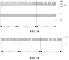
- the second photoresist layer is removed, and a fill layer 382 is formed which fills the first trench 40a, the second trench 40b and the third trench 40c, wherein the top surface of the fill layer 382 in each region is higher than the top surface of the intermediate layer 40 in the corresponding region.
- the fill layer 382 is formed by a spin-coating process which has a faster rate in layer formation and helps shorten the manufacturing process; furthermore, the material of the fill layer 382 comprises carbon or carbon-containing organic substances which are soft in texture and are easy to be etched and removed, thereby further shortening the manufacturing process of the semiconductor structure.
- the height difference between the top surface of the fill layer 382 in the first region 311 and the top surface of the fill layer 382 in the second region 312 is smaller than or equal to the first preset value, which helps prevent a portion of the fill layer 382 material in the second region 312 from sliding to the first region 311 due to lack of support; furthermore, the height difference between the top surface of the fill layer 382 in the first region 311 and the top surface of the fill layer 382 in the third region 313 is smaller than or equal to the second preset value which is greater than the first preset value, which helps prevent a portion of the fill layer material of the third region 313 from sliding to the first region 311 due to lack of support.
- the thickness of the fill layer 382 on the intermediate layer 40 in the first edge region 311a is equal to that in the first central region 311b, and the fill layers 382 on the intermediate layers 40 in the first region 311, the second region 312, and the third region 313 have the same thickness.
- the fill layer 382 has the same material as the first intermediate layer 401 such that the same etching agent can subsequently be used to etch a mixed layer composed of the first intermediate layer 401 and the remaining fill layer 382 at a fast rate to form the second opening and the third opening, thereby avoiding the problem of uneven etching and the further problem of an inaccurate opening pattern, guaranteeing the accurate formation of the second opening and the third opening, and performing accurate etching of the first mask layer 342.
- the maskless dry etching process is performed to remove a portion of the fill layer 382 in the first region 311 until the top surface of the sacrificial layer 372 is exposed and until the remaining fill layer 382 in the first region 311 fills the first trench 40a.
- the fill layer 382 on the intermediate layer 40 in the first region 311, the second region 312, and the third region 313 is removed in the same step of the process as the top surface of the sacrificial layer 372 in the first region 311, the second region 312, and the third region 313 is exposed.
- the maskless dry etching process can simultaneously expose the top surface of the sacrificial layer 371 in the first edge region 311a and the first central region 311b without having to over-etch the fill layer 382 in the first trench 40a to expose the top surface of the sacrificial layer 371 in the first edge region 311a after the top surface of the sacrificial layer 371 in the first central region 311b is exposed.
- the fill layer 382 in the first trench 40a tends to have good integrity, thereby ensuring that the first opening subsequently formed by etching the sacrificial layer 372 on the sidewall of the first trench 40a with the intermediate layer 40 and the fill layer as a mask meets the requirements of the preset pattern, and avoiding an oversized first opening caused by etching a portion of the fill layer 382 in the first trench 40a.
- a third photoresist layer 363 is formed, which has a third opening pattern disposed in the second region 312 and the third region 313; a mixed layer composed of the intermediate layer 40 and the remaining fill layer 382 is etched through the third opening pattern to form a second opening 40d disposed in the second region 312 and a third opening 40e disposed in the third region 313.
- the second opening 40d and the third opening 40e expose the top surface of the second isolation layer 392 such that the second isolation layer 392 exposed by the second opening 40d and the third opening 40e can be etched through in the subsequent process step of forming a first opening, with an additional process step of etching the second isolation layer 392 omitted and the etching time shortened.
- the third photoresist layer 363 is removed, and the sacrificial layer 372 on the sidewall of the first trench 40a in the first region 311 is etched to form a first opening 40f.
- the sacrificial layer 372 may be removed by a maskless dry etching process to etch through the second isolation layer 392 in the first region 311, the second region 312 and the third region 313 when forming the first opening 40f.
- the first opening 40f which has a second extending direction, has the same extending direction as the first trench 40a.
- a mask pattern identical to the target pattern may be formed on the first mask layer 342.
- the first extending direction is 120°
- the second extending direction is 60°
- a diamond-shaped target pattern may be formed on the first mask layer 342.
- the second opening 40d and the third opening 40e are formed before the formation of the first opening 40f, which prevents the third photoresist layer 363 (refer to FIG. 31 ) from falling into the first opening 40f, thereby reducing the difficulty in removing the third photoresist layer 363 and shortening the time of removing the third photoresist layer 363.
- the second isolation layer 392, the first isolation layer 391, and the first mask layer 342 are sequentially etched through the first opening 40f, the second opening 40d and the third opening 40e to form a second mask layer 344, which has the same mask pattern as the target pattern; after the second mask layer 344 is formed, the remaining isolation layer 39, the remaining intermediate layer 40, the remaining fill layer 382 and the remaining sacrificial layer 372 are removed.
- the protective layer 33 and the target layer 321 are sequentially etched using the second mask layer 344, wherein the remaining target layer 321 serves as the target pattern 322; after the target pattern 322 is formed, the second mask layer 344 and the remaining protective layer 33 are removed.
- the second trench is formed in the second region such that a portion of the fill layer material in the second region falls into the second trench, thereby reducing the height difference between the top surface of the fill layer in the first region and the top surface of the fill layer in the second region, avoiding a collapse of the fill layer in the second region whereby a portion of the material will slide to the top of the first region and exposing all the top surface of the sacrificial layer without over-etching in the subsequent maskless dry etching process. Therefore, a complete first opening is formed and selective etching is performed completely to the target layer.
Landscapes
- Engineering & Computer Science (AREA)
- Computer Hardware Design (AREA)
- Physics & Mathematics (AREA)
- Condensed Matter Physics & Semiconductors (AREA)
- General Physics & Mathematics (AREA)
- Manufacturing & Machinery (AREA)
- Microelectronics & Electronic Packaging (AREA)
- Power Engineering (AREA)
- Chemical & Material Sciences (AREA)
- Inorganic Chemistry (AREA)
- General Chemical & Material Sciences (AREA)
- Chemical Kinetics & Catalysis (AREA)
- Element Separation (AREA)
Abstract
Description
- The present application is based on
Chinese Patent Application No. 202110341446.0, filed on March 30, 2021 - The present application relates to the field of semiconductors, and in particular to a method for manufacturing a semiconductor structure.
- Before subjecting a layer to selective etching, it is generally necessary to form a mask layer with an opening pattern. The mask layer may be either a photoresist layer or a mask layer composed of one or more other materials. The opening pattern may be formed either by exposing and developing photoresist, or by etching particular materials in a composite layer which are generally formed in a particular position in advance and occupy the position of a to-be-formed opening pattern.
- However, the etching of a to-be-etched region may be affected by adjacent regions. For example, a particular material is covered and cannot be exposed to the etching agent such that a preset opening pattern cannot be formed, thereby subjecting the target layer to incomplete selective etching.
- The embodiment of the application provides a method of manufacturing a semiconductor structure, whereby selective etching can be performed completely to the target layer.
- To solve the above problems, the embodiment of the application provides a method of manufacturing a semiconductor structure, which comprises the following steps: providing a substrate, comprising a first region, a second region, and a third region, wherein the second region is disposed between the first region and the third region; forming a target layer, a first mask layer, an isolation layer and an intermediate layer sequentially on the substrate, wherein the intermediate layer in the first region has at least one first trench therein which exposes the isolation layer, and the bottom and the sidewall of the first trench are covered with a sacrificial layer; etching a portion of the intermediate layer in the second region to form at least one second trench which is disposed in the intermediate layer in the second region; forming a fill layer which fills the first trench and the second trench, wherein the top surface of the fill layer is higher than the top surface of the intermediate layer, and the height difference between the top surface of the fill layer in the first region and the top surface of the fill layer in the second region is smaller than or equal to a first preset value in the direction perpendicular to the top surface of the substrate; performing a maskless dry etching process to remove a portion of the fill layer in the first region until the top surface of the sacrificial layer is exposed and the remaining fill layer in the first region fills the first trench; removing the sacrificial layer which covers the sidewall of the first trench to form a first opening in the first region, wherein the first opening exposes the surface of the isolation layer; and etching sequentially a portion of the isolation layer, a portion of the first mask layer and a portion of the target layer in the first region through the first opening, whereby the remaining target layer forms a target pattern.
- In the above technical scheme, before the fill layer is formed, the second trench is formed in the second region such that a portion of the fill layer material in the second region falls into the second trench, thereby reducing the height difference between the top surface of the fill layer in the first region and the top surface of the fill layer in the second region, avoiding a collapse of the fill layer in the second region whereby a portion of the material will slide to the top of the first region and enabling all the top surface of the sacrificial layer to be exposed without over-etching in the subsequent maskless dry etching process. Therefore, a complete first opening is formed and selective etching is performed completely to the target layer.
- In addition, before removing the sacrificial layer on the sidewall of the first trench to form the first opening, the second opening and the third opening are formed, which prevents the photoresist layer used to form the second opening and the third opening from filling the first opening, thereby avoiding the trouble in removing the photoresist material which falls into the first opening and ensuring the effective execution of the subsequent etching process.
- One or more embodiments are illustrated by way of example with reference to the accompanying drawings, and the figures in the drawings are not to be limiting to scale unless specifically stated.
-
FIGS. 1 to 18 are schematic structure diagrams corresponding to each step in a method of manufacturing a semiconductor structure; -
FIGS. 19 to 35 are schematic structure diagrams corresponding to each step in the method of manufacturing a semiconductor structure provided by the embodiment of the present application. -
FIGS. 1 to 18 are schematic structure diagrams corresponding to each step in a method of manufacturing a semiconductor structure. The method thereof comprises the following steps: - Referring to
FIG. 1 , there is provided asubstrate 11, comprising afirst region 111, asecond region 112 and athird region 113, wherein thesecond region 112 is disposed between thefirst region 111 and thethird region 113; and atarget layer 121, aprotective layer 13, aninitial mask layer 141 and an initialintermediate layer 15 are formed on thesubstrate 11, which are stacked in sequence. - Referring to
FIG. 2 , afirst photoresist layer 161 having a first opening pattern is formed on the initialintermediate layer 15; and the initialintermediate layer 15 is etched with the first opening pattern to form anintermediate trench 15a which exposes the surface of theinitial mask layer 141. - The arrangement density of the
intermediate trenches 15a in thefirst region 111 is higher than the arrangement density of theintermediate trenches 15a in thesecond region 112, and the arrangement density of theintermediate trenches 15a in thesecond region 112 is higher than the arrangement density of theintermediate trenches 15a in thethird region 113. - Referring to
FIG. 3 , there is formed an initialsacrificial layer 171 covering the bottom and the sidewall of theintermediate trench 15a, and the initialsacrificial layer 171 also covers the tops of the initialintermediate layers 15 in thefirst region 111, thesecond region 112 and thethird region 113. - Referring to
FIG. 4 , a deposition process is performed to form aninitial fill layer 181 filling theintermediate trench 15a. - In performing a maskless deposition process, the deposition rates and the deposition time in different regions are the same. That is, the total material of the
initial fill layer 181 deposited per unit area in any region is the same. Since the arrangement density of theintermediate trenches 15a in thefirst region 111, thesecond region 112 and thethird region 113 decreases gradually, thefirst region 111 comprises the most number ofintermediate trenches 15a per unit area and thesecond region 112 comprises the second most number ofintermediate trenches 15a per unit area. The moreintermediate trenches 15a there are, the more the material of theinitial fill layer 181 can be accommodated, the less redundant material of theinitial fill layer 181 there will be left on the initialintermediate layer 15 and the lower the top surface of theinitial fill layer 181 will be. Accordingly, the top surface of theinitial fill layer 181 in thefirst region 111, thesecond region 112 and thethird region 113 rises gradually. - Referring to
FIGS. 5 and 6 , theinitial fill layer 181 is etched and the remaininginitial fill layer 181 exposes the top surface of the initialsacrificial layer 171 which covers the sidewall of theintermediate trench 15a; and the initialsacrificial layer 171 covering the sidewall of theintermediate trench 15a is etched to form aninitial gap 15b which exposes the surface of theinitial mask layer 141. - Herein, since the
initial mask layer 141 in thethird region 113 need not be etched, aninitial gap 15b need not be formed in thethird region 113. Accordingly, there is nointermediate trench 15a and initialsacrificial layer 171 in the initialintermediate layer 15 in thethird region 113, and theinitial fill layer 181 in thethird region 113 need not be removed. - Referring to
FIGS. 6 and7 , theinitial mask layer 141 is etched through theinitial gap 15b to form afirst mask layer 142; and the remaining initialintermediate layer 15, the remaining initialsacrificial layer 171 and the remaininginitial fill layer 181 are removed after thefirst mask layer 142 is formed. - The
first mask layer 142 has a plurality offourth openings 142a with the same opening width in a direction parallel to thesubstrate 11, wherein the width of thefourth opening 142a is equal to the thickness of the initialsacrificial layer 171 which covers the sidewall of theintermediate trench 15a; in addition, since the arrangement density of theintermediate trenches 15a in thefirst region 111, thesecond region 112 and thethird region 113 decreases gradually, the arrangement density of theinitial gaps 15b in thefirst region 111, thesecond region 112 and thethird region 113 decreases gradually, and the arrangement density of thefourth openings 142a in thefirst region 111, thesecond region 112 and thethird region 113 decreases gradually. - Referring to
FIG. 8 , there is formed on thefirst mask layer 142 anisolation layer 19 and anintermediate layer 20 stacked in sequence. - Since the arrangement density of the
fourth openings 142a in thefirst region 111, thesecond region 112 and thethird region 113 decreases gradually, the top surface of theisolation layer 19 in thefirst region 111, thesecond region 112, and thethird region 113 gradually rises when theisolation layer 19 and theintermediate layer 20 are uniformly deposited in different regions. Accordingly, the top surface of theintermediate layer 20 in thefirst region 111, thesecond region 112 and thethird region 113 gradually rises. - Referring to
FIG. 9 , there is formed in theintermediate layer 20 in thefirst region 111 at least onefirst trench 20a, which exposes the surface of theisolation layer 19; and there is formed a firstsacrificial layer 172 which covers the bottom and the sidewall of thefirst trench 20a and the top surface of theintermediate layer 20 in thefirst region 111, thesecond region 112 and thethird region 113. - Referring to
FIG. 10 , a secondphotoresist layer 162 is formed which fills thefirst trench 20a and is disposed on theintermediate layer 20 in thefirst region 111, thesecond region 112, and thethird region 113. The secondphotoresist layer 162 has a second opening pattern disposed in thethird region 113. - Referring to
FIG. 11 , the firstsacrificial layer 172 and theintermediate layer 20 are etched with the second opening pattern to form a third trench 20C which is disposed in theintermediate layer 20 in thethird region 113; and the second photoresist layer is removed after the third trench 20C is formed. - Referring to
FIG. 12 , afill layer 182 is formed which fills thefirst trench 20a and thethird trench 20c, and the upper surface of thefill layer 182 is higher than the upper surface of theintermediate layer 20. - Since the deposition processes have the same deposition rate and deposition time in different regions, the total material of the
fill layer 182 deposited per unit area in any region is the same. The top surface positions of thefill layer 182 in the different regions depend on two factors: one is the top surface position of theintermediate layer 20 in a region and the other is the arrangement density and the opening width of the trenches or the openings in theintermediate layer 20 in a region. The higher the top surface of theintermediate layer 20 is, the higher the top surface of thefill layer 182 is. Whereas the higher the arrangement density and the opening width of the trenches or openings in theintermediate layer 20 is, the lower the top surface of thefill layer 182 is. - Specifically, the top surface of the
intermediate layer 20 in thefirst region 111 is lower than the top surface of theintermediate layer 20 in thesecond region 112, and theintermediate layer 20 in thefirst region 111 has thefirst trench 20a therein while theintermediate layer 20 in thesecond region 112 does not have a trench or an opening therein. Accordingly, the top surface of thefill layer 182 in thefirst region 111 is lower than the top surface of thefill layer 182 in thesecond region 112. - When the difference between the height of the top surface of the
fill layer 182 in thefirst region 111 and the height of the top surface of thefill layer 182 in thesecond region 112 is bigger than the first preset value, a portion of thefill layer 182 material at the edge of thesecond region 112 may collapse for lack of support and may slide toward afirst edge region 111a in thefirst region 111, such that the top surface of thefill layer 182 in thefirst edge region 111a is higher. In other words, thefill layer 182 on theintermediate layer 20 in thefirst edge region 111a is thicker, whereas thefill layer 182 on theintermediate layer 20 in the firstcentral region 111b is thinner. - Further, if the
fill layer 182 is formed using a spin-coating process, the whole structure of thefill layer 182 will be loose and the strength of the structure will be low, thereby making the layer prone to collapse for lack of support. Accordingly, if the material of thefill layer 182 is carbon or a carbon-containing organic substance, thefill layer 182 which will have a softer texture, lower hardness and lower structure strength is also prone to collapse for lack of support. - In addition, although the top surface of the
intermediate layer 20 in thesecond region 112 is lower than the top surface of theintermediate layer 20 in thethird region 113, theintermediate layer 20 in thethird region 113 has the third trenches 20C therein such that the top surface of thefill layer 182 in thethird region 113 may be higher or lower than or flush with the top surface of thefill layer 182 in thesecond region 112 as the third trenches 20C vary in arrangement density and opening width. - When the top surface of the
fill layer 182 in thethird region 113 is higher than the top surface of thefill layer 182 in thesecond region 112, a portion of thefill layer 182 material in thethird region 113 may collapse for lack of support and may slide to thesecond region 112 or even thefirst region 111, such that the top surface of thefill layer 182 in thefirst edge region 111a is higher; and when the top surface of thefill layer 182 in thethird region 113 is lower than the top surface of thefill layer 182 in thesecond region 112, a portion of thefill layer 182 material in thesecond region 112 may slide to thethird region 113, thereby lowering the top surface of thefill layer 182 in thesecond region 112 and reducing the height difference between the top surface of thefill layer 182 in thefirst region 111 and the top surface of thefill layer 182 in thesecond region 112, which helps prevent a portion of thefill layer 182 material in thesecond region 112 from sliding to thefirst region 111. - Referring to
FIG. 13 , thefill layer 182 is etched using a maskless dry etching process. - In the process of a maskless dry etching, the to-be-etched
fill layers 182 in different regions have the same thickness. If thefill layer 182 on theintermediate layer 20 in thefirst edge region 111a is thicker and thefill layer 182 on theintermediate layer 20 in the firstcentral region 111b is thinner, the top surface of the firstsacrificial layer 172 in thefirst edge region 111a is still covered by thefill layer 182 when the top surface of the firstsacrificial layer 172 in the firstcentral region 111b is exposed. - Referring to
FIGS. 14 and15 , the firstsacrificial layer 172 on the sidewall of thefirst trench 20a is etched to form a first opening 20b; theisolation layer 19 and thefirst mask layer 142 are sequentially etched through the first opening 20b to form asecond mask layer 143; and after thesecond mask layer 143 is formed, theremaining isolation layer 19, the remainingintermediate layer 20, the remaining firstsacrificial layer 172 and theremaining fill layer 182 are removed. - Since the
fill layer 182 is still left on theintermediate layer 20 in thefirst edge region 111a, the firstsacrificial layer 172 which covers the sidewall of thefirst trench 20a has not been completely etched. Therefore, the pattern of the first opening 20b is incomplete, and the opening pattern of thesecond mask layer 143 which is formed by etching through the first opening 20b is also incomplete. - Referring to
FIG. 16 , atransfer layer 21 and athird photoresist layer 163 are formed which are sequentially stacked, wherein thethird photoresist layer 163 has a third opening pattern disposed in thesecond region 112 and thethird region 113. - Referring to
FIGS. 17 and 18 , thetransfer layer 21 and thesecond mask layer 143 are sequentially etched using the third opening pattern to form athird mask layer 144; and after thethird mask layer 144 is formed, the remainingtransfer layer 21 and thethird photoresist layer 163 are removed, and theprotective layer 13 and thetarget layer 121 are sequentially etched through the opening pattern of thethird mask layer 144, wherein the remainingtarget layer 121 serves as thetarget pattern 122. - Since the opening pattern of the
second mask layer 143 is incomplete, the opening pattern of thethird mask layer 144 and the ultimately formedtarget pattern 122 are incomplete. - In order to further clarify the purpose, technical schemes and advantages of the embodiment of the present application, the embodiment of the present application will be described in detail with reference to the accompanying drawings. However, one of ordinary skill in the art will appreciate that in the embodiment of the present application a plurality of technical details have been presented for readers to better understand this application. However, even without these technical details and various changes and modifications based on the following embodiment the technical schemes claimed herein may be realized.
-
FIGS. 19 to 35 are schematic structure diagrams corresponding to each step of the method of manufacturing a semiconductor structure provided by the embodiment of the present application. The method comprises the following steps: - Referring to
FIG. 19 , there is provided asubstrate 31, comprising afirst region 311, asecond region 312 and athird region 313, wherein thesecond region 312 is disposed between thefirst region 311 and thethird region 313; and there are formed on the substrate 31 atarget layer 321, aprotective layer 33, aninitial mask layer 341 and an initialintermediate layer 35 which are sequentially stacked. - In the present embodiment, the
first region 311 is an array region, thesecond region 312 is a core region, and thethird region 313 is a peripheral region. The array region, the core region and the peripheral region all comprise a bit line structure, and the arrangement density of the bit line structures in the array region is higher than the arrangement density of the bit line structures in the core region and in the peripheral region. - It should be noted that the
first region 311, thesecond region 312, and thethird region 313 refer to the different regions of the semiconductor structure which are divided with reference to thesubstrate 31, and do not simply refer to the different parts of thesubstrate 31. Thefirst region 311 comprises a portion of thesubstrate 31 and other layers formed on thesubstrate 31. - In the present embodiment, the
protective layer 33 comprises a firstprotective layer 331 and a secondprotective layer 332 stacked in sequence, wherein the secondprotective layer 332 has a higher hardness than theinitial mask layer 341 and can be used as a hard mask layer complementary to theinitial mask layer 341. Specifically, the material of theinitial mask layer 341 comprises silicon dioxide and the material of the secondprotective layer 332 comprises silicon oxynitride. The initialintermediate layer 35 comprises a first initialintermediate layer 351 and a second initialintermediate layer 352 which are sequentially stacked, and the first initialintermediate layer 351 having the same material as the secondprotective layer 332 can be used as a hard mask layer complementary to a subsequently formed photoresist layer on the initialintermediate layer 35. - The first
protective layer 331 may have a lower hardness than the secondprotective layer 332 in order to shorten the duration of the etching process and to avoid damages to thetarget layer 321; and similarly, the first initialintermediate layer 351 may have a lower hardness than the second initialintermediate layer 352 in order to shorten the duration of the etching process and to avoid damages to theinitial mask layer 341. - Referring to
FIG. 20 , afirst photoresist layer 361 having a first opening pattern is formed on the initialintermediate layer 35; and the initialintermediate layer 35 is etched through the first opening pattern to form anintermediate trench 35a which exposes the surface of theinitial mask layer 341. - In the embodiment, the arrangement density of the
intermediate trenches 35a of thefirst region 311 is higher than the arrangement density of theintermediate trenches 35a in thesecond region 312, and the arrangement density of theintermediate trenches 35a in thesecond region 312 is higher than the arrangement density of theintermediate trenches 35a in thethird region 313; in addition, the first opening pattern and theintermediate trench 35a have a first extending direction, and specifically the first extending direction may be 120°. - Referring to
FIG. 21 , an initialsacrificial layer 371 is formed, which covers the bottom and the sidewall of theintermediate trench 35a as well as the top surfaces of the initialintermediate layer 35 in thefirst region 311, thesecond region 312 and thethird region 313. - Before the initial
sacrificial layer 371 is formed, thefirst photoresist layer 361 needs to be removed; and the initialsacrificial layer 371 may have the same material as theinitial mask layer 341, which helps to lessen the types of materials required for the semiconductor manufacturing process and to reduce the cost and the complexity of the semiconductor manufacturing process. - Referring to
FIG. 22 , a deposition process is performed to form aninitial fill layer 381 filling theintermediate trench 35a. - In performing a maskless deposition process, the deposition rates and the deposition time in different regions are the same, that is, the total material of the
initial fill layer 381 deposited per unit area in any region is the same. Since the arrangement density of theintermediate trenches 35a in thefirst region 311, thesecond region 312 and thethird region 313 decreases gradually, thefirst region 311 comprises the most number ofintermediate trenches 35a per unit area and thesecond region 312 comprises the second most number ofintermediate trenches 35a per unit area. The moreintermediate trenches 35a there are, the more the material of theinitial fill layer 381 can be accommodated, the less redundant material of theinitial fill layer 381 there will be left on the initialintermediate layer 35 and the lower the top surface of theinitial fill layer 381 will be. Accordingly, the top surface of theinitial fill layer 381 in thefirst region 311, thesecond region 312 and thethird region 313 rises gradually. - Referring to
FIGS. 23 and24 , theinitial fill layer 381 is etched and the remaininginitial fill layer 381 exposes the top surface of the initialsacrificial layer 371 which covers the sidewall of theintermediate trench 35a; and the initialsacrificial layer 371 which covers the sidewall of theintermediate trench 35a is etched to form aninitial gap 35b which exposes the surface of theinitial mask layer 341. - In the present document, since the
initial mask layer 341 in thethird region 313 need not be etched, aninitial gap 35b need not be formed in thethird region 313. Accordingly, there is nointermediate trench 35a and no initialsacrificial layer 371 in the initialintermediate layer 35 in thethird region 313, and theinitial fill layer 381 in thethird region 313 need not be removed. - Referring to
FIGS. 24 and 25 , theinitial mask layer 341 is etched through theinitial gap 35b to form afirst mask layer 342; and the remaining initialintermediate layer 35, the remaining initialsacrificial layer 371 and the remaininginitial fill layer 381 are removed after thefirst mask layer 342 is formed. - The
first mask layer 342 has a plurality offourth openings 342a with the same opening width in a direction parallel to thesubstrate 31, wherein the width is equal to the thickness of the initialsacrificial layer 371 which covers the sidewall of theintermediate trench 35a; and thefourth opening 342a which has a first extending direction has the same extending direction as theintermediate trench 35a,; in addition, since the arrangement density of theintermediate trenches 35a in thefirst region 311, thesecond region 312 and thethird region 313 decreases gradually, the arrangement density of theinitial gaps 35b in thefirst region 311, thesecond region 312 and thethird region 313 decreases gradually, and the arrangement density of thefourth openings 342a in thefirst region 311, thesecond region 312 and thethird region 313 decreases gradually. - Referring to
FIG. 26 , there is formed on thefirst mask layer 342 anisolation layer 39 and anintermediate layer 40 stacked in sequence. - Since the arrangement density of the
fourth openings 342a in thefirst region 311, thesecond region 312 and thethird region 313 decreases gradually, the top surface of theisolation layer 39 in thefirst region 311, thesecond region 312, and thethird region 313 gradually rises when theisolation layer 39 and theintermediate layer 40 are uniformly deposited in different regions, and the top surface of theintermediate layer 40 in thefirst region 311, thesecond region 312 and thethird region 313 gradually rises. - In the embodiment, the
isolation layer 39 comprises afirst isolation layer 391 and asecond isolation layer 392 stacked in sequence, wherein thefirst isolation layer 391 has a lower hardness than thesecond isolation layer 392 but a bigger thickness than thesecond isolation layer 392, which helps shorten the etching duration of theisolation layer 39; and theintermediate layer 40 comprises a firstintermediate layer 401 and a secondintermediate layer 402 stacked in sequence, wherein the firstintermediate layer 401 has a lower hardness than the secondintermediate layer 402 but a bigger thickness than the secondintermediate layer 402, which helps shorten the etching duration of theintermediate layer 40. - The
second isolation layer 392 may have the same material as thefirst mask layer 342, the firstintermediate layer 401 may have the same material as thefirst isolation layer 391, the secondintermediate layer 402 is used as a hard mask layer, and the secondintermediate layer 402 may have the same material as the secondprotective layer 332, which helps lessen the types of materials required for the semiconductor manufacturing process and the types of etching agents and reduce the cost and the complexity of the semiconductor manufacturing process. - Referring to
FIG. 27 , at least onefirst trench 40a is formed in theintermediate layer 40 in thefirst region 311, wherein thefirst trench 40a exposes the surface of theisolation layer 39; and asacrificial layer 372 is formed, wherein thesacrificial layer 372 covers the bottom and the sidewall of thefirst trench 40a as well as the top surface of theintermediate layer 40 which covers thefirst region 311, thesecond region 312 and thethird region 313. - In the embodiment, the
first region 311 comprises afirst edge region 311a adjacent to thesecond region 312 and a firstcentral region 311b remote from thesecond region 312, wherein thefirst trench 40a is at least partially disposed in thefirst edge region 311a and thesacrificial layer 372 covering the sidewall of thefirst trench 40a is at least partially disposed in thefirst edge region 311a; in addition, thesacrificial layer 372 may have the same material as thesecond isolation layer 392. - In the embodiment, the
first trench 40a has a second extending direction, for example, a direction of 60°. The orthographic projection of the first extending direction is diagonal to the orthographic projection of the second extending direction in a plane parallel to thesubstrate 31. - Referring to
FIG. 28 , asecond photoresist layer 362 is formed, which fills thefirst trench 40a and is disposed on theintermediate layer 40 in thefirst region 311, thesecond region 312, and thethird region 313. And thesecond photoresist layer 362 has a second opening pattern, through which theintermediate layer 40 is etched. - In the embodiment, the second opening pattern of the
second photoresist layer 362 is disposed at least in thesecond region 312, and theintermediate layer 40 is etched with the second opening pattern to form at least onesecond trench 40b in thesecond region 312, which helps the subsequently formed fill layer partially fill into thesecond trench 40b, thereby reducing the difference between the height of the top surface of the fill layer in thefirst region 311 and the height of the top surface of the fill layer in thesecond region 312, preventing a portion of the fill layer material in thesecond region 312 from sliding to thefirst region 311 for lack of support, and ensuring that the thickness of the fill layer on theintermediate layer 40 in thefirst edge region 311a and thefirst center region 31 1b of thefirst region 311 remains the same. - In the embodiment, the
second trench 40b has a smaller opening width than thefirst trench 40a in a direction parallel to thesubstrate 31, thereby avoiding etching through thesecond isolation layer 392 due to the etch loading effect, ensuring the isolating effect of thesecond isolation layer 392 and avoiding etching thefirst isolation layer 391 and thefirst mask layer 342 in case thesecond isolation layer 392 is etched through; meanwhile, the arrangement density of thesecond trenches 40b is higher than the arrangement density of thefirst trenches 40a, which helps thesecond trenches 40b in thesecond region 312 accommodate more fill layer material, so that the height difference between the top surface of the fill layer in thefirst region 311 and the top surface of the fill layer in thesecond region 312 is small after the fill layer is formed and the fill layer material in thesecond region 312 is prevented from sliding to thefirst region 311. - Further, the thickness of the subsequently formed fill layer on the
intermediate layer 40 in thefirst region 311 and in thesecond region 312 is equaled by adjusting the opening width and the arrangement density of thesecond trenches 40b. Therefore, after the fill layer is formed, the fill layer on theintermediate layer 40 in thefirst region 311 and thesecond region 312 can be etched by the same maskless dry etching process to expose the top surface of thesacrificial layer 372. - In the embodiment, the second opening pattern of the
second photoresist layer 362 is also disposed in thethird region 313. In the same process as etching a portion of theintermediate layer 40 in thesecond region 312 through the second opening pattern, a portion of theintermediate layer 40 in thethird region 313 is etched to form athird trench 40c. Therefore, thethird trench 40c in thethird region 313 can accommodate a portion of the subsequently deposited fill layer material, which helps prevent the fill layer material in thethird region 313 from sliding to thefirst region 311 and helps a portion of the fill layer material in thesecond region 312 slide to thethird region 313, thereby further reducing the height difference between the top surface of the fill layer in thefirst region 311 and the top surface of the fill layer in thesecond region 312 in a direction perpendicular to the top surface of thesubstrate 31. - It should be noted that when the
second region 312, due to external restrictions, cannot have thesecond trenches 40b formed in high arrangement density, a portion of the fill layer material in thesecond region 312 is directed to slide to thethird region 313, which can ease to some extent the problem of the low arrangement density of thesecond trenches 40b in thesecond region 312, ensure that the height difference between the top surface of the fill layer in thefirst region 311 and the top surface of the fill layer in thesecond region 312 is smaller than a first preset value, and prevent a portion of the fill layer material in thesecond region 312 from sliding to thefirst region 311. - In the embodiment, the opening width of the
third trench 40c is equal to the opening width of thesecond trench 40b and the arrangement density of thethird trenches 40c is equal to the arrangement density of thesecond trenches 40b. By providing both thesecond trench 40c and thethird trench 40c with the same accommodating capacity per unit area, the fill layer on theintermediate layer 40 in thesecond region 312 and the fill layer on theintermediate layer 40 in thethird region 313 can have same thickness in the process of depositing the fill layer, so that after the fill layer is formed, the fill layer on theintermediate layer 40 in thefirst region 311, thesecond region 312 and thethird region 313 can be etched by the same maskless dry etching process to expose thesacrificial layer 372. - Referring to
FIG. 29 , the second photoresist layer is removed, and afill layer 382 is formed which fills thefirst trench 40a, thesecond trench 40b and thethird trench 40c, wherein the top surface of thefill layer 382 in each region is higher than the top surface of theintermediate layer 40 in the corresponding region. - In the embodiment, the
fill layer 382 is formed by a spin-coating process which has a faster rate in layer formation and helps shorten the manufacturing process; furthermore, the material of thefill layer 382 comprises carbon or carbon-containing organic substances which are soft in texture and are easy to be etched and removed, thereby further shortening the manufacturing process of the semiconductor structure. - In the embodiment, the height difference between the top surface of the
fill layer 382 in thefirst region 311 and the top surface of thefill layer 382 in thesecond region 312 is smaller than or equal to the first preset value, which helps prevent a portion of thefill layer 382 material in thesecond region 312 from sliding to thefirst region 311 due to lack of support; furthermore, the height difference between the top surface of thefill layer 382 in thefirst region 311 and the top surface of thefill layer 382 in thethird region 313 is smaller than or equal to the second preset value which is greater than the first preset value, which helps prevent a portion of the fill layer material of thethird region 313 from sliding to thefirst region 311 due to lack of support. - In addition, the thickness of the
fill layer 382 on theintermediate layer 40 in thefirst edge region 311a is equal to that in the firstcentral region 311b, and the fill layers 382 on theintermediate layers 40 in thefirst region 311, thesecond region 312, and thethird region 313 have the same thickness. - In the embodiment, the
fill layer 382 has the same material as the firstintermediate layer 401 such that the same etching agent can subsequently be used to etch a mixed layer composed of the firstintermediate layer 401 and the remainingfill layer 382 at a fast rate to form the second opening and the third opening, thereby avoiding the problem of uneven etching and the further problem of an inaccurate opening pattern, guaranteeing the accurate formation of the second opening and the third opening, and performing accurate etching of thefirst mask layer 342. - Referring to
FIG. 30 , the maskless dry etching process is performed to remove a portion of thefill layer 382 in thefirst region 311 until the top surface of thesacrificial layer 372 is exposed and until the remainingfill layer 382 in thefirst region 311 fills thefirst trench 40a. - In the embodiment, the
fill layer 382 on theintermediate layer 40 in thefirst region 311, thesecond region 312, and thethird region 313 is removed in the same step of the process as the top surface of thesacrificial layer 372 in thefirst region 311, thesecond region 312, and thethird region 313 is exposed. - Since the thickness of the
fill layer 382 on theintermediate layer 40 in thefirst edge region 311a is equal to that in the first central region 3 11b, the maskless dry etching process can simultaneously expose the top surface of thesacrificial layer 371 in thefirst edge region 311a and the firstcentral region 311b without having to over-etch thefill layer 382 in thefirst trench 40a to expose the top surface of thesacrificial layer 371 in thefirst edge region 311a after the top surface of thesacrificial layer 371 in the firstcentral region 311b is exposed. Accordingly, thefill layer 382 in thefirst trench 40a tends to have good integrity, thereby ensuring that the first opening subsequently formed by etching thesacrificial layer 372 on the sidewall of thefirst trench 40a with theintermediate layer 40 and the fill layer as a mask meets the requirements of the preset pattern, and avoiding an oversized first opening caused by etching a portion of thefill layer 382 in thefirst trench 40a. - In addition, since the
fill layer 382 on theintermediate layer 40 in thesecond region 312 and thethird region 313 is removed simultaneously, no separate etching processes need to be performed to selectively remove the remainingfill layer 382 on theintermediate layer 40 in thesecond region 312 and thethird region 313 before the formation of the second opening and the third opening, which helps shorten the duration of manufacturing the semiconductor structure; further, as thefill layer 382 in thesecond trench 40b and thethird trench 40c is not over-etched by the maskless dry etching process, there will not be the problem of an oversized opening caused by over-etching, thereby ensuring the accuracy of the patterns of the second opening and the third opening which are formed later by etching a mixed layer composed of theintermediate layer 40 and the remainingfill layer 382. - Referring to
FIG. 31 , athird photoresist layer 363 is formed, which has a third opening pattern disposed in thesecond region 312 and thethird region 313; a mixed layer composed of theintermediate layer 40 and the remainingfill layer 382 is etched through the third opening pattern to form asecond opening 40d disposed in thesecond region 312 and athird opening 40e disposed in thethird region 313. - In the embodiment, the
second opening 40d and thethird opening 40e expose the top surface of thesecond isolation layer 392 such that thesecond isolation layer 392 exposed by thesecond opening 40d and thethird opening 40e can be etched through in the subsequent process step of forming a first opening, with an additional process step of etching thesecond isolation layer 392 omitted and the etching time shortened. - Referring to
FIGS. 32 and 33 , thethird photoresist layer 363 is removed, and thesacrificial layer 372 on the sidewall of thefirst trench 40a in thefirst region 311 is etched to form afirst opening 40f. - In the embodiment, the
sacrificial layer 372 may be removed by a maskless dry etching process to etch through thesecond isolation layer 392 in thefirst region 311, thesecond region 312 and thethird region 313 when forming thefirst opening 40f. - In addition, the
first opening 40f, which has a second extending direction, has the same extending direction as thefirst trench 40a. When thefirst mask layer 342 is etched through thefirst opening 40f, a mask pattern identical to the target pattern may be formed on thefirst mask layer 342. Specifically, the first extending direction is 120°, the second extending direction is 60°, and a diamond-shaped target pattern may be formed on thefirst mask layer 342. - In addition, the
second opening 40d and thethird opening 40e are formed before the formation of thefirst opening 40f, which prevents the third photoresist layer 363 (refer toFIG. 31 ) from falling into thefirst opening 40f, thereby reducing the difficulty in removing thethird photoresist layer 363 and shortening the time of removing thethird photoresist layer 363. - Referring to
FIGS. 33 and34 , thesecond isolation layer 392, thefirst isolation layer 391, and thefirst mask layer 342 are sequentially etched through thefirst opening 40f, thesecond opening 40d and thethird opening 40e to form asecond mask layer 344, which has the same mask pattern as the target pattern; after thesecond mask layer 344 is formed, the remainingisolation layer 39, the remainingintermediate layer 40, the remainingfill layer 382 and the remainingsacrificial layer 372 are removed. - Referring to
FIGS. 34 and 35 , theprotective layer 33 and thetarget layer 321 are sequentially etched using thesecond mask layer 344, wherein the remainingtarget layer 321 serves as thetarget pattern 322; after thetarget pattern 322 is formed, thesecond mask layer 344 and the remainingprotective layer 33 are removed. - In the embodiment, before the formation of the fill layer, the second trench is formed in the second region such that a portion of the fill layer material in the second region falls into the second trench, thereby reducing the height difference between the top surface of the fill layer in the first region and the top surface of the fill layer in the second region, avoiding a collapse of the fill layer in the second region whereby a portion of the material will slide to the top of the first region and exposing all the top surface of the sacrificial layer without over-etching in the subsequent maskless dry etching process. Therefore, a complete first opening is formed and selective etching is performed completely to the target layer.
- It will be apparent to one of ordinary skill in the art that the above described embodiments are specific embodiments to implement the present application and that in practical application various revisions in form and detail may be made thereto without departing from the spirit and scope of the present application. Any person skilled in the art may make their own revisions and modifications without departing from the spirit and scope of the present application, so the scope of protection of the present application shall be subject to the scope defined by the claims.
Claims (15)
- A method for manufacturing a semiconductor structure, comprising:providing a substrate, comprising a first region, a second region, and a third region, wherein the second region is disposed between the first region and the third region;forming a target layer, a first mask layer, an isolation layer and an intermediate layer sequentially on the substrate, wherein the intermediate layer in the first region has at least one first trench therein which exposes the isolation layer, and the bottom and the sidewall of the first trench are covered with a sacrificial layer;etching a portion of the intermediate layer in the second region to form at least one second trench which is disposed in the intermediate layer in the second region;forming a fill layer which fills the first trench and the second trench, wherein the top surface of the fill layer is higher than the top surface of the intermediate layer; and the height difference between the top surface of the fill layer in the first region and the top surface of the fill layer in the second region is smaller than or equal to a first preset value in the direction perpendicular to the top surface of the substrate;performing a maskless dry etching process to remove a portion of the fill layer in the first region until the top surface of the sacrificial layer is exposed and until the remaining fill layer in the first region fills the first trench;removing the sacrificial layer which covers the sidewall of the first trench to form a first opening in the first region, wherein the first opening exposes the surface of the isolation layer; andetching sequentially a portion of the isolation layer, a portion of the first mask layer and a portion of the target layer in the first region through the first opening, whereby the remaining target layer forms a target pattern.
- The method of claim 1, wherein the opening width of the second trench is smaller than the opening width of the first trench and the arrangement density of the second trenches is higher than the arrangement density of the first trenches.
- The method of claim 1, wherein, in the same process step of etching a portion of the intermediate layer in the second region, a portion of the intermediate layer in the third region is etched to form a third trench in the third region;
and the fill layer fills the third trench, and in the direction perpendicular to the top surface of the substrate the height difference between the top surface of the fill layer in the first region and the top surface of the fill layer in the third region is smaller than or equal to a second preset value which is higher than the first preset value. - The method of claim 3, wherein the opening width of the third trench is equal to the opening width of the second trench and the arrangement density of the third trenches is equal to the arrangement density of the second trenches.
- The method of claim 3, wherein the first region is an array region, the second region is a core region and the third region is a peripheral region.
- The method of claim 1, wherein before the sacrificial layer on the sidewall of the first trench is removed, a further step is comprised:
etching a portion of the intermediate layer in the second region and a portion of the intermediate layer in the third region to form a second opening and a third opening; wherein the second opening is disposed in the second region and the third opening is disposed in the third region. - The method of claim 6, wherein the second opening and the third opening expose the top surface of the isolation layer.
- The method of claim 6, wherein in the same process step of sequentially etching a portion of the isolation layer, a portion of the first mask layer and a portion of the target layer on the first region through the first opening, further steps are comprised:
etching sequentially a portion of the isolation layer, a portion of the first mask layer and a portion of the target layer in the second region through the second opening, and etching sequentially a portion of the isolation layer, a portion of the first mask layer and a portion of the target layer in the third region through the third opening. - The method of claim 6, wherein the material of the fill layer is the same as that of the intermediate layer.
- The method of claim 1, wherein the first mask layer has a plurality of fourth openings, which have the same opening width in the direction parallel to the substrate, have a first extending direction parallel to the surface of the substrate and are filled with the isolation layer.
- The method of claim 10, wherein the arrangement density of the fourth openings in the first region is higher the arrangement density of the fourth openings that in the second region, the top surface of the isolation layer in the second region is higher than the top surface of the isolation layer in the first region, and the top surface of the intermediate layer in the second region is higher than the top surface of the intermediate layer in the first region.
- The method of claim 10, wherein the arrangement density of the fourth openings in the second region is higher than the arrangement density of the fourth openings in the third region, the top surface of the isolation layer in the third region is higher than the top surface of the isolation layer in the second region, and the top surface of the intermediate layer in the third region is higher than the top surface of the intermediate layer in the second region.
- The method of claim 10, wherein the first opening has a second extending direction parallel to the surface of the substrate, and the orthographic projection of the first extending direction is diagonal to the orthographic projection of the second extending direction in a plane parallel to the substrate.
- The method of claim 10, wherein the process of forming the first mask layer comprises the steps of:providing the substrate, the target layer and the initial mask layer stacked in sequence;forming on the initial mask layer an initial intermediate layer and a photoresist layer stacked in sequence, wherein the photoresist layer has an opening pattern with the first extending direction;etching the initial intermediate layer through the opening pattern to form an intermediate trench which exposes the surface of the initial mask layer;forming an initial sacrificial layer which covers the bottom and the sidewall of the intermediate trench, and forming an initial fill layer which fills the intermediate trench, wherein the initial fill layer exposes the top surface of the initial sacrificial layer;removing the initial sacrificial layer which covers the sidewall of the intermediate trench to form an initial gap which exposes the surface of the initial mask layer;etching the initial mask layer through the initial gap to form a first mask layer; andremoving the remaining initial intermediate layer, the remaining initial sacrificial layer and the remaining initial fill layer after the first mask layer is formed.
- The method of claim 1, wherein the fill layer is formed by a spin-coating process, and the material of the fill layer comprises carbon or a carbon-containing compound.
Applications Claiming Priority (2)
| Application Number | Priority Date | Filing Date | Title |
|---|---|---|---|
| CN202110341446.0A CN113078056B (en) | 2021-03-30 | 2021-03-30 | Method for manufacturing semiconductor structure |
| PCT/CN2021/112301 WO2022205736A1 (en) | 2021-03-30 | 2021-08-12 | Method for manufacturing semiconductor structure |
Publications (2)
| Publication Number | Publication Date |
|---|---|
| EP4199043A1 true EP4199043A1 (en) | 2023-06-21 |
| EP4199043A4 EP4199043A4 (en) | 2024-07-10 |
Family
ID=83448358
Family Applications (1)
| Application Number | Title | Priority Date | Filing Date |
|---|---|---|---|
| EP21934380.3A Pending EP4199043A4 (en) | 2021-03-30 | 2021-08-12 | Method for manufacturing semiconductor structure |
Country Status (2)
| Country | Link |
|---|---|
| US (1) | US12046472B2 (en) |
| EP (1) | EP4199043A4 (en) |
Family Cites Families (7)
| Publication number | Priority date | Publication date | Assignee | Title |
|---|---|---|---|---|
| KR100905827B1 (en) * | 2006-09-29 | 2009-07-02 | 주식회사 하이닉스반도체 | Method for forming hard mask pattern in semiconductor device |
| KR20090010399A (en) * | 2007-07-23 | 2009-01-30 | 삼성전자주식회사 | Method of forming fine patterns of semiconductor device using double patterning process |
| KR101566405B1 (en) * | 2009-01-07 | 2015-11-05 | 삼성전자주식회사 | Method of forming patterns of semiconductor device |
| KR102564402B1 (en) * | 2018-12-07 | 2023-08-08 | 에스케이하이닉스 주식회사 | Method for fabricating a semiconductor device |
| TWI761827B (en) * | 2020-05-05 | 2022-04-21 | 力晶積成電子製造股份有限公司 | Semiconductor patterning process |
| US20230343641A1 (en) * | 2020-12-29 | 2023-10-26 | Western Digital Technologies, Inc. | Method of making a three-dimensional memory device using composite hard masks for formation of deep via openings |
| KR20220110379A (en) * | 2021-01-29 | 2022-08-08 | 삼성전자주식회사 | semiconductor device and manufacturing method thereof |
-
2021
- 2021-08-12 EP EP21934380.3A patent/EP4199043A4/en active Pending
- 2021-11-22 US US17/456,071 patent/US12046472B2/en active Active
Also Published As
| Publication number | Publication date |
|---|---|
| US12046472B2 (en) | 2024-07-23 |
| EP4199043A4 (en) | 2024-07-10 |
| US20220319848A1 (en) | 2022-10-06 |
Similar Documents
| Publication | Publication Date | Title |
|---|---|---|
| US8822285B2 (en) | Nonvolatile memory device and method of manufacturing the same | |
| US20120156866A1 (en) | Method of forming patterns of semiconductor device | |
| US20090130852A1 (en) | Process for improving critical dimension uniformity of integrated circuit arrays | |
| TWI477999B (en) | Method for fabricating semiconductor device using spacer patterning technique | |
| TW201814829A (en) | Apparatus and method of forming self-aligned cuts in a non-mandrel line of an array of metal lines | |
| US20230209823A1 (en) | Method of manufacturing memory device and patterning method | |
| US6713884B2 (en) | Method of forming an alignment mark structure using standard process steps for forming vertical gate transistors | |
| CN113078056B (en) | Method for manufacturing semiconductor structure | |
| EP4199043A1 (en) | Method for manufacturing semiconductor structure | |
| US8399955B2 (en) | Method of forming patterns of semiconductor device | |
| CN110707004B (en) | Semiconductor device and method of forming the same | |
| US7816270B2 (en) | Method of forming minute patterns in semiconductor device using double patterning | |
| CN112447582A (en) | Method for forming trench isolation structure in substrate | |
| CN210607187U (en) | Memory device | |
| CN111341725B (en) | Method for manufacturing semiconductor pattern | |
| CN115206979A (en) | Memory assembly and manufacturing method thereof | |
| JP4330523B2 (en) | Method for forming dummy layer of split gate flash memory device | |
| US20210265378A1 (en) | Manufacturing method of semiconductor memory device and semiconductor memory device | |
| CN111640752B (en) | Memory and forming method thereof | |
| KR101082719B1 (en) | Method of manufacturing patterns for a semiconductor device | |
| CN113725166B (en) | Semiconductor structure preparation method and semiconductor structure | |
| CN211182204U (en) | Memory device | |
| US20240297051A1 (en) | Method for manufacturing semiconductor device | |
| US20230402314A1 (en) | Method for manufacturing semiconductor device, and semiconductor device | |
| US7060561B2 (en) | Method for fabricating memory device |
Legal Events
| Date | Code | Title | Description |
|---|---|---|---|
| STAA | Information on the status of an ep patent application or granted ep patent |
Free format text: STATUS: THE INTERNATIONAL PUBLICATION HAS BEEN MADE |
|
| PUAI | Public reference made under article 153(3) epc to a published international application that has entered the european phase |
Free format text: ORIGINAL CODE: 0009012 |
|
| STAA | Information on the status of an ep patent application or granted ep patent |
Free format text: STATUS: REQUEST FOR EXAMINATION WAS MADE |
|
| 17P | Request for examination filed |
Effective date: 20230317 |
|
| AK | Designated contracting states |
Kind code of ref document: A1 Designated state(s): AL AT BE BG CH CY CZ DE DK EE ES FI FR GB GR HR HU IE IS IT LI LT LU LV MC MK MT NL NO PL PT RO RS SE SI SK SM TR |
|
| REG | Reference to a national code |
Ref country code: DE Ref legal event code: R079 Free format text: PREVIOUS MAIN CLASS: H01L0021308000 Ipc: H01L0021033000 |
|
| A4 | Supplementary search report drawn up and despatched |
Effective date: 20240612 |
|
| DAV | Request for validation of the european patent (deleted) | ||
| DAX | Request for extension of the european patent (deleted) | ||
| RIC1 | Information provided on ipc code assigned before grant |
Ipc: H01L 21/311 20060101ALI20240606BHEP Ipc: H01L 21/033 20060101AFI20240606BHEP |