EP4198984A1 - Adaptive control circuit of static random access memory - Google Patents
Adaptive control circuit of static random access memory Download PDFInfo
- Publication number
- EP4198984A1 EP4198984A1 EP22210449.9A EP22210449A EP4198984A1 EP 4198984 A1 EP4198984 A1 EP 4198984A1 EP 22210449 A EP22210449 A EP 22210449A EP 4198984 A1 EP4198984 A1 EP 4198984A1
- Authority
- EP
- European Patent Office
- Prior art keywords
- transistor
- node
- control circuit
- adaptive control
- terminal coupled
- Prior art date
- Legal status (The legal status is an assumption and is not a legal conclusion. Google has not performed a legal analysis and makes no representation as to the accuracy of the status listed.)
- Granted
Links
Images




Classifications
-
- G—PHYSICS
- G11—INFORMATION STORAGE
- G11C—STATIC STORES
- G11C11/00—Digital stores characterised by the use of particular electric or magnetic storage elements; Storage elements therefor
- G11C11/21—Digital stores characterised by the use of particular electric or magnetic storage elements; Storage elements therefor using electric elements
- G11C11/34—Digital stores characterised by the use of particular electric or magnetic storage elements; Storage elements therefor using electric elements using semiconductor devices
- G11C11/40—Digital stores characterised by the use of particular electric or magnetic storage elements; Storage elements therefor using electric elements using semiconductor devices using transistors
- G11C11/41—Digital stores characterised by the use of particular electric or magnetic storage elements; Storage elements therefor using electric elements using semiconductor devices using transistors forming static cells with positive feedback, i.e. cells not needing refreshing or charge regeneration, e.g. bistable multivibrator or Schmitt trigger
- G11C11/412—Digital stores characterised by the use of particular electric or magnetic storage elements; Storage elements therefor using electric elements using semiconductor devices using transistors forming static cells with positive feedback, i.e. cells not needing refreshing or charge regeneration, e.g. bistable multivibrator or Schmitt trigger using field-effect transistors only
-
- G—PHYSICS
- G11—INFORMATION STORAGE
- G11C—STATIC STORES
- G11C11/00—Digital stores characterised by the use of particular electric or magnetic storage elements; Storage elements therefor
- G11C11/21—Digital stores characterised by the use of particular electric or magnetic storage elements; Storage elements therefor using electric elements
- G11C11/34—Digital stores characterised by the use of particular electric or magnetic storage elements; Storage elements therefor using electric elements using semiconductor devices
- G11C11/40—Digital stores characterised by the use of particular electric or magnetic storage elements; Storage elements therefor using electric elements using semiconductor devices using transistors
- G11C11/41—Digital stores characterised by the use of particular electric or magnetic storage elements; Storage elements therefor using electric elements using semiconductor devices using transistors forming static cells with positive feedback, i.e. cells not needing refreshing or charge regeneration, e.g. bistable multivibrator or Schmitt trigger
- G11C11/413—Auxiliary circuits, e.g. for addressing, decoding, driving, writing, sensing, timing or power reduction
- G11C11/417—Auxiliary circuits, e.g. for addressing, decoding, driving, writing, sensing, timing or power reduction for memory cells of the field-effect type
-
- G—PHYSICS
- G11—INFORMATION STORAGE
- G11C—STATIC STORES
- G11C11/00—Digital stores characterised by the use of particular electric or magnetic storage elements; Storage elements therefor
- G11C11/21—Digital stores characterised by the use of particular electric or magnetic storage elements; Storage elements therefor using electric elements
- G11C11/34—Digital stores characterised by the use of particular electric or magnetic storage elements; Storage elements therefor using electric elements using semiconductor devices
- G11C11/40—Digital stores characterised by the use of particular electric or magnetic storage elements; Storage elements therefor using electric elements using semiconductor devices using transistors
- G11C11/41—Digital stores characterised by the use of particular electric or magnetic storage elements; Storage elements therefor using electric elements using semiconductor devices using transistors forming static cells with positive feedback, i.e. cells not needing refreshing or charge regeneration, e.g. bistable multivibrator or Schmitt trigger
- G11C11/413—Auxiliary circuits, e.g. for addressing, decoding, driving, writing, sensing, timing or power reduction
- G11C11/417—Auxiliary circuits, e.g. for addressing, decoding, driving, writing, sensing, timing or power reduction for memory cells of the field-effect type
- G11C11/419—Read-write [R-W] circuits
-
- H—ELECTRICITY
- H03—ELECTRONIC CIRCUITRY
- H03K—PULSE TECHNIQUE
- H03K4/00—Generating pulses having essentially a finite slope or stepped portions
- H03K4/94—Generating pulses having essentially a finite slope or stepped portions having trapezoidal shape
-
- G—PHYSICS
- G11—INFORMATION STORAGE
- G11C—STATIC STORES
- G11C7/00—Arrangements for writing information into, or reading information out from, a digital store
- G11C7/10—Input/output [I/O] data interface arrangements, e.g. I/O data control circuits, I/O data buffers
- G11C7/1078—Data input circuits, e.g. write amplifiers, data input buffers, data input registers, data input level conversion circuits
- G11C7/1084—Data input buffers, e.g. comprising level conversion circuits, circuits for adapting load
-
- G—PHYSICS
- G11—INFORMATION STORAGE
- G11C—STATIC STORES
- G11C7/00—Arrangements for writing information into, or reading information out from, a digital store
- G11C7/22—Read-write [R-W] timing or clocking circuits; Read-write [R-W] control signal generators or management
- G11C7/225—Clock input buffers
Definitions
- the disclosure generally relates to a control circuit, and more specifically, to an adaptive control circuit of SRAM (Static Random Access Memory).
- SRAM Static Random Access Memory
- the disclosure is directed to an adaptive control circuit of SRAM (Static Random Access Memory).
- the adaptive control circuit includes a switch circuit, a forward diode-connected transistor, a backward diode-connected transistor, and a first delay circuit.
- the switch circuit is supplied by a supply voltage, and is coupled to a first node.
- the backward diode-connected transistor is coupled in parallel with the forward diode-connected transistor between the first node and a second node.
- the first delay circuit is coupled between the second node and a ground voltage.
- the forward diode-connected transistor will be enabled if the supply voltage is higher than or equal to a threshold voltage.
- the switch circuit includes a first transistor.
- the first transistor has a control terminal for receiving a clock voltage, a first terminal coupled to the supply voltage, and a second terminal coupled to the first node.
- the first transistor is implemented with a PMOSFET (P-type Metal-Oxide-Semiconductor Field-Effect Transistor).
- PMOSFET P-type Metal-Oxide-Semiconductor Field-Effect Transistor
- the forward diode-connected transistor is a second transistor which has a control terminal coupled to the first node, a first terminal coupled to the second node, and a second terminal coupled to the first node.
- the second transistor is implemented with an NMOSFET (N-type Metal-Oxide-Semiconductor Field-Effect Transistor).
- NMOSFET N-type Metal-Oxide-Semiconductor Field-Effect Transistor
- the backward diode-connected transistor is a third transistor which has a control terminal coupled to the second node, a first terminal coupled to the first node, and a second terminal coupled to the second node.
- the third transistor is implemented with an NMOSFET.
- the first delay circuit is a capacitive element or a resistive element.
- the first delay circuit includes a fourth transistor.
- the fourth transistor has a control terminal coupled to the second node, a first terminal coupled to the ground voltage, and a second terminal coupled to the ground voltage.
- the fourth transistor is implemented with an NMOSFET.
- the switch circuit further includes a fifth transistor.
- the fifth transistor has a control terminal for receiving the clock voltage, a first terminal coupled to the ground voltage, and a second terminal coupled to the first node.
- the fifth transistor is implemented with an NMOSFET.
- the adaptive control circuit further includes a second delay circuit coupled to the first node.
- the second delay circuit includes a sixth transistor.
- the sixth transistor has a control terminal coupled to the ground voltage, a first terminal coupled to the first node, and a second terminal coupled to the ground voltage.
- the sixth transistor is implemented with an NMOSFET.
- the adaptive control circuit further includes a third delay circuit coupled to the first node.
- the third delay circuit includes a seventh transistor.
- the seventh transistor has a control terminal coupled to the first node, a first terminal coupled to the ground voltage, and a second terminal coupled to the ground voltage.
- the seventh transistor is implemented with an NMOSFET.
- the adaptive control circuit further includes an inverter.
- the inverter has an input terminal coupled to the first node, and a second terminal coupled to an output node.
- FIG. 1 is a diagram of an adaptive control circuit 100 of SRAM (Static Random Access Memory) according to an embodiment of the invention.
- the adaptive control circuit 100 includes a switch circuit 110, a forward diode-connected transistor 120, a backward diode-connected transistor 130, and a first delay circuit 140.
- the switch circuit 110 is supplied by a supply voltage VCC, and is coupled to a first node N1.
- the supply voltage VCC is variable.
- the supply voltage VCC may have any voltage level which is higher than or equal to 0.4V, but it is not limited thereto.
- the backward diode-connected transistor 130 is coupled in parallel with the forward diode-connected transistor 120 between the first node N1 and a second node N2.
- the first delay circuit 140 is coupled between the second node N2 and the ground voltage VSS.
- the ground voltage VSS may have a voltage level of OV.
- the first delay circuit 140 may be a capacitive element or a resistive element, but it is not limited thereto.
- both the forward diode-connected transistor 120 and the backward diode-connected transistor 130 will be disabled.
- the forward diode-connected transistor 120 will be enabled (the backward diode-connected transistor 130 may also be enabled).
- the aforementioned threshold voltage may be equal to 0.6V, but it is not limited thereto.
- the enabled forward diode-connected transistor 120 can conduct a first current I1 from the first node N1 to the second node N2.
- the backward diode-connected transistor 130 is enabled, it will conduct a second current 12 from the second node N2 to the first node N1, so as to make the first delay circuit 140 return to its initial state.
- this design for the adaptive control circuit 100 not only provides an acceptable operational speed but also maintains a sufficient read margin.
- the operational speed of the adaptive control circuit 100 may be at least 100MHz, and the read margin of the adaptive control circuit 100 may be at least 100mV, but they are not limited thereto. Therefore, the proposed adaptive control circuit 100 will have good operational performance even if it is supplied by the variable supply voltage VCC.
- FIG. 2 is a circuit diagram of an adaptive control circuit 200 of SRAM according to an embodiment of the invention.
- the adaptive control circuit 200 includes a switch circuit 210, a forward diode-connected transistor 220, a backward diode-connected transistor 230, and a first delay circuit 240.
- the switch circuit 210 includes a first transistor M1.
- the first transistor M1 has a control terminal (e.g., a gate) for receiving a clock voltage VA, a first terminal (e.g., a source/drain) coupled to a supply voltage VCC, and a second terminal (e.g., another source/drain) coupled to a first node N1.
- the forward diode-connected transistor 220 is a second transistor M2 which has a control terminal (e.g., a gate) coupled to the first node N1, a first terminal (e.g., a source/drain) coupled to a second node N2, and a second terminal (e.g., another source/drain) coupled to the first node N1.
- the backward diode-connected transistor 230 is a third transistor M3 which has a control terminal (e.g., a gate) coupled to the second node N2, a first terminal (e.g., a source/drain) coupled to the first node N1, and a second terminal (e.g., another source/drain) coupled to the second node N2.
- the first delay circuit 240 includes a fourth transistor M4.
- the fourth transistor M4 has a control terminal (e.g., a gate) coupled to the second node N2, a first terminal (e.g., a source/drain) coupled to the ground voltage VSS, and a second terminal (e.g., another source/drain) coupled to the ground voltage VSS.
- the first transistor M1 is implemented with a PMOSFET (P-type Metal-Oxide-Semiconductor Field-Effect Transistor), and each of the second transistor M2, the third transistor M3, and the fourth transistor M4 is implemented with an NMOSFET (N-type Metal-Oxide-Semiconductor Field-Effect Transistor).
- PMOSFET P-type Metal-Oxide-Semiconductor Field-Effect Transistor
- NMOSFET N-type Metal-Oxide-Semiconductor Field-Effect Transistor
- the first transistor M1 will be enabled to pre-charge the first node N1. Conversely, if the clock voltage VA has a high logic level, the first transistor M1 will stop pre-charging the first node N1.
- the second transistor M2 is configured to selectively conduct a first current I1 from the first node N1 to the second node N2.
- the third transistor M3 is configured to selectively conduct a second current 12 from the second node N2 to the first node N1.
- the fourth transistor M4 is used as a small-size chip capacitor.
- Other features of the adaptive control circuit 200 of FIG. 2 are similar to those of the adaptive control circuit 100 of FIG. 1 . Therefore, the two embodiments can achieve similar levels of performance.
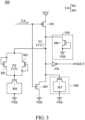
- FIG. 3 is a circuit diagram of an adaptive control circuit 300 of SRAM according to an embodiment of the invention.
- FIG. 3 is similar to FIG. 2 .
- a switch circuit 310 of the adaptive control circuit 300 further includes a fifth transistor M5
- the adaptive control circuit 300 further includes a second delay circuit 350, a third delay circuit 360, and an inverter 370.
- the second delay circuit 350, the third delay circuit 360, and the inverter 370 are all coupled to the first node N1.
- the fifth transistor M5 has a control terminal (e.g., a gate) for receiving the clock voltage VA, a first terminal (e.g., a source/drain) coupled to the ground voltage VSS, and a second terminal (e.g., another source/drain) coupled to the first node N1.
- the second delay circuit 350 includes a sixth transistor M6.
- the sixth transistor M6 has a control terminal (e.g., a gate) coupled to the ground voltage VSS, a first terminal (e.g., a source/drain) coupled to the first node N1, and a second terminal (e.g., another source/drain) coupled to the ground voltage VSS.
- the third delay circuit 360 includes a seventh transistor M7.
- the seventh transistor M7 has a control terminal (e.g., a gate) coupled to the first node N1, a first terminal (e.g., a source/drain) coupled to the ground voltage VSS, and a second terminal (e.g., another source/drain) coupled to the ground voltage VSS.
- each of the fifth transistor M5, the sixth transistor M6, and the seventh transistor M7 is implemented with an NMOSFET.
- the inverter 370 has an input terminal coupled to the first node N1, and a second terminal coupled to an output node NOUT.
- the adaptive control circuit 300 is a tracking circuit for controlling a cell array of SRAM (not shown). If the clock voltage VA has a low logic level, the fifth transistor M5 will be disabled. Conversely, if the clock voltage VA has a high logic level, the fifth transistor M5 will be enabled to discharge the first node N1.
- each of the second delay circuit 350 and the third delay circuit 360 is a capacitive element or a resistive element with a different circuit design.
- the output node NOUT of the adaptive control circuit 300 is arranged to output the control voltage for controlling the relative circuitry of SRAM (not shown).
- Other features of the adaptive control circuit 300 of FIG. 3 are similar to those of the adaptive control circuit 200 of FIG. 2 . Therefore, the two embodiments can achieve similar levels of performance.
- FIG. 4 is a diagram of voltage waveforms of the adaptive control circuit 300 according to an embodiment of the invention.
- the horizontal axis represents the time.
- the vertical axes represent the voltage levels of the clock voltage VA, a first voltage V1 at the first node N1, and a second voltage V2 at the second node N2.
- the clock voltage VA rises to a high logic level
- the first voltage V1 at the first node N1 will become lower
- the clock voltage VA drops to a low logic level
- the first voltage V1 at the first node N1 will become higher.
- the second voltage V2 at the second node N2 has relatively small variations since it is limited by both the second transistor M2 and the third transistor M3.
- FIG. 5 is a diagram of the relationship between the read margin and the supply voltage VCC of the adaptive control circuit 300 according to an embodiment of the invention.
- the horizontal axis represents the voltage level of the supply voltage VCC.
- the vertical axis represents the voltage level of the read margin.
- the read margin of the adaptive control circuit 300 is always greater than a minimum voltage level VL, regardless of the variations of the supply voltage VCC.
- the minimum voltage level VL may be equal to 100m V, but it is not limited thereto. Therefore, the adaptive control circuit 300 can keep a sufficient read margin.
- the read margin of the adaptive control circuit 300 is also enhanced by the fourth transistor M4 used as a chip capacitor.
- the charge and dis-charge current to the capacitance is adaptively limited for a wide-voltage range operation. Hence, the corresponding operational speed can achieve a quite acceptable target (e.g., faster than 100MHz).
- the invention proposes an adaptive control circuit of SRAM. Compared to the conventional design, the invention has at least the advantages of the adaptive supply voltage, the wide-range operation, the sufficient read margin, the low leakage, and the fast operational speed, and therefore it is suitable for application in a variety of electronic devices.
- the adaptive control circuit of the invention is not limited to the configurations of FIGS. 1-5 .
- the invention may merely include any one or more features of any one or more embodiments of FIGS. 1-5 . In other words, not all of the features displayed in the figures should be implemented in the adaptive control circuit of the invention.
- MOSFET Metal-Oxide-Semiconductor Field-Effect Transistor
- the invention is not limited thereto, and those skilled in the art may use other types of transistors, such as BJT (Bipolar Junction Transistor), JFET (Junction Gate Field Effect Transistor), FinFET (Fin Field Effect Transistor), etc., without affecting the performance of the invention.
- BJT Bipolar Junction Transistor
- JFET Junction Gate Field Effect Transistor
- FinFET Fin Field Effect Transistor
Landscapes
- Engineering & Computer Science (AREA)
- Microelectronics & Electronic Packaging (AREA)
- Computer Hardware Design (AREA)
- Static Random-Access Memory (AREA)
Abstract
Description
- The disclosure generally relates to a control circuit, and more specifically, to an adaptive control circuit of SRAM (Static Random Access Memory).
- In a conventional design, if the control circuit of a SRAM (Static Random Access Memory) is supplied by a variable supply voltage, the corresponding read margin of the control circuit may be insufficient. Furthermore, the control circuit may suffer from a slow operational speed. Accordingly, there is a need to propose a novel solution for solving the problems of the prior art.
- In an exemplary embodiment, the disclosure is directed to an adaptive control circuit of SRAM (Static Random Access Memory). The adaptive control circuit includes a switch circuit, a forward diode-connected transistor, a backward diode-connected transistor, and a first delay circuit. The switch circuit is supplied by a supply voltage, and is coupled to a first node. The backward diode-connected transistor is coupled in parallel with the forward diode-connected transistor between the first node and a second node. The first delay circuit is coupled between the second node and a ground voltage.
- In some embodiments, if the supply voltage is higher than or equal to a threshold voltage, the forward diode-connected transistor will be enabled.
- In some embodiments, the switch circuit includes a first transistor. The first transistor has a control terminal for receiving a clock voltage, a first terminal coupled to the supply voltage, and a second terminal coupled to the first node.
- In some embodiments, the first transistor is implemented with a PMOSFET (P-type Metal-Oxide-Semiconductor Field-Effect Transistor).
- In some embodiments, the forward diode-connected transistor is a second transistor which has a control terminal coupled to the first node, a first terminal coupled to the second node, and a second terminal coupled to the first node.
- In some embodiments, the second transistor is implemented with an NMOSFET (N-type Metal-Oxide-Semiconductor Field-Effect Transistor).
- In some embodiments, the backward diode-connected transistor is a third transistor which has a control terminal coupled to the second node, a first terminal coupled to the first node, and a second terminal coupled to the second node.
- In some embodiments, the third transistor is implemented with an NMOSFET.
- In some embodiments, the first delay circuit is a capacitive element or a resistive element.
- In some embodiments, the first delay circuit includes a fourth transistor. The fourth transistor has a control terminal coupled to the second node, a first terminal coupled to the ground voltage, and a second terminal coupled to the ground voltage.
- In some embodiments, the fourth transistor is implemented with an NMOSFET.
- In some embodiments, the switch circuit further includes a fifth transistor. The fifth transistor has a control terminal for receiving the clock voltage, a first terminal coupled to the ground voltage, and a second terminal coupled to the first node.
- In some embodiments, the fifth transistor is implemented with an NMOSFET.
- In some embodiments, the adaptive control circuit further includes a second delay circuit coupled to the first node.
- In some embodiments, the second delay circuit includes a sixth transistor. The sixth transistor has a control terminal coupled to the ground voltage, a first terminal coupled to the first node, and a second terminal coupled to the ground voltage.
- In some embodiments, the sixth transistor is implemented with an NMOSFET.
- In some embodiments, the adaptive control circuit further includes a third delay circuit coupled to the first node.
- In some embodiments, the third delay circuit includes a seventh transistor. The seventh transistor has a control terminal coupled to the first node, a first terminal coupled to the ground voltage, and a second terminal coupled to the ground voltage.
- In some embodiments, the seventh transistor is implemented with an NMOSFET.
- In some embodiments, the adaptive control circuit further includes an inverter. The inverter has an input terminal coupled to the first node, and a second terminal coupled to an output node.
- The invention can be more fully understood by reading the subsequent detailed description and examples with references made to the accompanying drawings, wherein:
-
FIG. 1 is a diagram of an adaptive control circuit of SRAM (Static Random Access Memory) according to an embodiment of the invention; -
FIG. 2 is a circuit diagram of an adaptive control circuit of SRAM according to an embodiment of the invention; -
FIG. 3 is a circuit diagram of an adaptive control circuit of SRAM according to an embodiment of the invention; -
FIG. 4 is a diagram of voltage waveforms of an adaptive control circuit according to an embodiment of the invention; and -
FIG. 5 is a diagram of the relationship between a read margin and a supply voltage of an adaptive control circuit according to an embodiment of the invention. - In order to illustrate the purposes, features and advantages of the invention, the embodiments and figures of the invention will be described in detail as follows.
- Certain terms are used throughout the description and following claims to refer to particular components. As one skilled in the art will appreciate, manufacturers may refer to a component by different names. This document does not intend to distinguish between components that differ in name but not function. In the following description and in the claims, the terms "include" and "comprise" are used in an open-ended fashion, and thus should be interpreted to mean "include, but not limited to...". The term "substantially" means the value is within an acceptable error range. One skilled in the art can solve the technical problem within a predetermined error range and achieve the proposed technical performance. Also, the term "couple" is intended to mean either an indirect or direct electrical connection. Accordingly, if one device is coupled to another device, that connection may be through a direct electrical connection, or through an indirect electrical connection via other devices and connections.
-
FIG. 1 is a diagram of anadaptive control circuit 100 of SRAM (Static Random Access Memory) according to an embodiment of the invention. As shown inFIG. 1 , theadaptive control circuit 100 includes aswitch circuit 110, a forward diode-connectedtransistor 120, a backward diode-connectedtransistor 130, and afirst delay circuit 140. Theswitch circuit 110 is supplied by a supply voltage VCC, and is coupled to a first node N1. The supply voltage VCC is variable. For example, the supply voltage VCC may have any voltage level which is higher than or equal to 0.4V, but it is not limited thereto. The backward diode-connectedtransistor 130 is coupled in parallel with the forward diode-connectedtransistor 120 between the first node N1 and a second node N2. Thefirst delay circuit 140 is coupled between the second node N2 and the ground voltage VSS. For example, the ground voltage VSS may have a voltage level of OV. Thefirst delay circuit 140 may be a capacitive element or a resistive element, but it is not limited thereto. - In some embodiments, if the supply voltage VCC is lower than a threshold voltage, both the forward diode-connected
transistor 120 and the backward diode-connectedtransistor 130 will be disabled. In alternative embodiments, if the supply voltage VCC is higher than or equal to the threshold voltage, the forward diode-connectedtransistor 120 will be enabled (the backward diode-connectedtransistor 130 may also be enabled). For example, the aforementioned threshold voltage may be equal to 0.6V, but it is not limited thereto. The enabled forward diode-connectedtransistor 120 can conduct a first current I1 from the first node N1 to the second node N2. On the other hand, if the backward diode-connectedtransistor 130 is enabled, it will conduct a second current 12 from the second node N2 to the first node N1, so as to make thefirst delay circuit 140 return to its initial state. - According to practical measurements, this design for the
adaptive control circuit 100 not only provides an acceptable operational speed but also maintains a sufficient read margin. For example, the operational speed of theadaptive control circuit 100 may be at least 100MHz, and the read margin of theadaptive control circuit 100 may be at least 100mV, but they are not limited thereto. Therefore, the proposedadaptive control circuit 100 will have good operational performance even if it is supplied by the variable supply voltage VCC. - The following embodiments will introduce different configurations and detail structural features of the
adaptive control circuit 100. It should be understood that these figures and descriptions are merely exemplary, rather than limitations of the invention. -
FIG. 2 is a circuit diagram of anadaptive control circuit 200 of SRAM according to an embodiment of the invention. In the embodiment ofFIG. 2 , theadaptive control circuit 200 includes aswitch circuit 210, a forward diode-connectedtransistor 220, a backward diode-connectedtransistor 230, and afirst delay circuit 240. - The
switch circuit 210 includes a first transistor M1. The first transistor M1 has a control terminal (e.g., a gate) for receiving a clock voltage VA, a first terminal (e.g., a source/drain) coupled to a supply voltage VCC, and a second terminal (e.g., another source/drain) coupled to a first node N1. The forward diode-connectedtransistor 220 is a second transistor M2 which has a control terminal (e.g., a gate) coupled to the first node N1, a first terminal (e.g., a source/drain) coupled to a second node N2, and a second terminal (e.g., another source/drain) coupled to the first node N1. The backward diode-connectedtransistor 230 is a third transistor M3 which has a control terminal (e.g., a gate) coupled to the second node N2, a first terminal (e.g., a source/drain) coupled to the first node N1, and a second terminal (e.g., another source/drain) coupled to the second node N2. Thefirst delay circuit 240 includes a fourth transistor M4. The fourth transistor M4 has a control terminal (e.g., a gate) coupled to the second node N2, a first terminal (e.g., a source/drain) coupled to the ground voltage VSS, and a second terminal (e.g., another source/drain) coupled to the ground voltage VSS. In some embodiments, the first transistor M1 is implemented with a PMOSFET (P-type Metal-Oxide-Semiconductor Field-Effect Transistor), and each of the second transistor M2, the third transistor M3, and the fourth transistor M4 is implemented with an NMOSFET (N-type Metal-Oxide-Semiconductor Field-Effect Transistor). - If the clock voltage VA has a low logic level, the first transistor M1 will be enabled to pre-charge the first node N1. Conversely, if the clock voltage VA has a high logic level, the first transistor M1 will stop pre-charging the first node N1. The second transistor M2 is configured to selectively conduct a first current I1 from the first node N1 to the second node N2. The third transistor M3 is configured to selectively conduct a second current 12 from the second node N2 to the first node N1. The fourth transistor M4 is used as a small-size chip capacitor. Other features of the
adaptive control circuit 200 ofFIG. 2 are similar to those of theadaptive control circuit 100 ofFIG. 1 . Therefore, the two embodiments can achieve similar levels of performance. -
FIG. 3 is a circuit diagram of anadaptive control circuit 300 of SRAM according to an embodiment of the invention.FIG. 3 is similar toFIG. 2 . In the embodiment ofFIG. 3 , aswitch circuit 310 of theadaptive control circuit 300 further includes a fifth transistor M5, and theadaptive control circuit 300 further includes asecond delay circuit 350, athird delay circuit 360, and aninverter 370. Thesecond delay circuit 350, thethird delay circuit 360, and theinverter 370 are all coupled to the first node N1. - The fifth transistor M5 has a control terminal (e.g., a gate) for receiving the clock voltage VA, a first terminal (e.g., a source/drain) coupled to the ground voltage VSS, and a second terminal (e.g., another source/drain) coupled to the first node N1. The
second delay circuit 350 includes a sixth transistor M6. The sixth transistor M6 has a control terminal (e.g., a gate) coupled to the ground voltage VSS, a first terminal (e.g., a source/drain) coupled to the first node N1, and a second terminal (e.g., another source/drain) coupled to the ground voltage VSS. Thethird delay circuit 360 includes a seventh transistor M7. The seventh transistor M7 has a control terminal (e.g., a gate) coupled to the first node N1, a first terminal (e.g., a source/drain) coupled to the ground voltage VSS, and a second terminal (e.g., another source/drain) coupled to the ground voltage VSS. In some embodiments, each of the fifth transistor M5, the sixth transistor M6, and the seventh transistor M7 is implemented with an NMOSFET. Theinverter 370 has an input terminal coupled to the first node N1, and a second terminal coupled to an output node NOUT. - In the embodiment of
FIG. 3 , theadaptive control circuit 300 is a tracking circuit for controlling a cell array of SRAM (not shown). If the clock voltage VA has a low logic level, the fifth transistor M5 will be disabled. Conversely, if the clock voltage VA has a high logic level, the fifth transistor M5 will be enabled to discharge the first node N1. In alternative embodiments, each of thesecond delay circuit 350 and thethird delay circuit 360 is a capacitive element or a resistive element with a different circuit design. The output node NOUT of theadaptive control circuit 300 is arranged to output the control voltage for controlling the relative circuitry of SRAM (not shown). Other features of theadaptive control circuit 300 ofFIG. 3 are similar to those of theadaptive control circuit 200 ofFIG. 2 . Therefore, the two embodiments can achieve similar levels of performance. -
FIG. 4 is a diagram of voltage waveforms of theadaptive control circuit 300 according to an embodiment of the invention. The horizontal axis represents the time. The vertical axes represent the voltage levels of the clock voltage VA, a first voltage V1 at the first node N1, and a second voltage V2 at the second node N2. According to the measurement ofFIG. 4 , if the clock voltage VA rises to a high logic level, the first voltage V1 at the first node N1 will become lower, and if the clock voltage VA drops to a low logic level, the first voltage V1 at the first node N1 will become higher. It should be noted that the second voltage V2 at the second node N2 has relatively small variations since it is limited by both the second transistor M2 and the third transistor M3. -
FIG. 5 is a diagram of the relationship between the read margin and the supply voltage VCC of theadaptive control circuit 300 according to an embodiment of the invention. The horizontal axis represents the voltage level of the supply voltage VCC. The vertical axis represents the voltage level of the read margin. According to the measurement ofFIG. 5 , the read margin of theadaptive control circuit 300 is always greater than a minimum voltage level VL, regardless of the variations of the supply voltage VCC. For example, the minimum voltage level VL may be equal to 100m V, but it is not limited thereto. Therefore, theadaptive control circuit 300 can keep a sufficient read margin. It should be understood that the read margin of theadaptive control circuit 300 is also enhanced by the fourth transistor M4 used as a chip capacitor. Furthermore, because of thecontrol circuit 200, the charge and dis-charge current to the capacitance is adaptively limited for a wide-voltage range operation. Hence, the corresponding operational speed can achieve a quite acceptable target (e.g., faster than 100MHz). - The invention proposes an adaptive control circuit of SRAM. Compared to the conventional design, the invention has at least the advantages of the adaptive supply voltage, the wide-range operation, the sufficient read margin, the low leakage, and the fast operational speed, and therefore it is suitable for application in a variety of electronic devices.
- It should be noted that the above voltages, currents, resistances, inductances, capacitances and other element parameters are not limitations of the invention. A designer can adjust these settings according to different requirements. The adaptive control circuit of the invention is not limited to the configurations of
FIGS. 1-5 . The invention may merely include any one or more features of any one or more embodiments ofFIGS. 1-5 . In other words, not all of the features displayed in the figures should be implemented in the adaptive control circuit of the invention. Although the embodiments of the invention use MOSFET (Metal-Oxide-Semiconductor Field-Effect Transistor) as examples, the invention is not limited thereto, and those skilled in the art may use other types of transistors, such as BJT (Bipolar Junction Transistor), JFET (Junction Gate Field Effect Transistor), FinFET (Fin Field Effect Transistor), etc., without affecting the performance of the invention. - Use of ordinal terms such as "first", "second", "third", etc., in the claims to modify a claim element does not by itself connote any priority, precedence, or order of one claim element over another or the temporal order in which acts of a method are performed, but are used merely as labels to distinguish one claim element having a certain name from another element having the same name (but for use of the ordinal term) to distinguish the claim elements.
- While the invention has been described by way of example and in terms of the preferred embodiments, it should be understood that the invention is not limited to the disclosed embodiments. On the contrary, it is intended to cover various modifications and similar arrangements (as would be apparent to those skilled in the art). Therefore, the scope of the appended claims should be accorded the broadest interpretation so as to encompass all such modifications and similar arrangements.
Claims (15)
- An adaptive control circuit of SRAM (Static Random Access Memory), comprising:a switch circuit, supplied by a supply voltage, and coupled to a first node;a forward diode-connected transistor;a backward diode-connected transistor, coupled in parallel with the forward diode-connected transistor between the first node and a second node; anda first delay circuit, coupled between the second node and a ground voltage.
- The adaptive control circuit as claimed in claim 1, wherein if the supply voltage is higher than or equal to a threshold voltage, the forward diode-connected transistor is enabled.
- The adaptive control circuit as claimed in claim 1 or 2, wherein the switch circuit comprises:
a first transistor, wherein the first transistor has a control terminal for receiving a clock voltage, a first terminal coupled to the supply voltage, and a second terminal coupled to the first node. - The adaptive control circuit as claimed in claim 3, wherein the first transistor is implemented with a PMOSFET (P-type Metal-Oxide-Semiconductor Field-Effect Transistor).
- The adaptive control circuit as claimed in any one of the preceding claims, wherein the forward diode-connected transistor is a second transistor which has a control terminal coupled to the first node, a first terminal coupled to the second node, and a second terminal coupled to the first node.
- The adaptive control circuit as claimed in claim 5, wherein the second transistor is implemented with an NMOSFET (N-type Metal-Oxide-Semiconductor Field-Effect Transistor).
- The adaptive control circuit as claimed in any one of the preceding claims, wherein the backward diode-connected transistor is a third transistor which has a control terminal coupled to the second node, a first terminal coupled to the first node, and a second terminal coupled to the second node.
- The adaptive control circuit as claimed in any one of the preceding claims, wherein the first delay circuit is a capacitive element or a resistive element.
- The adaptive control circuit as claimed in any one of claims 1 to 7, wherein the first delay circuit comprises:
a fourth transistor, wherein the fourth transistor has a control terminal coupled to the second node, a first terminal coupled to the ground voltage, and a second terminal coupled to the ground voltage. - The adaptive control circuit as claimed in claim 3 and in any claim that is dependent on claim 3, wherein the switch circuit further comprises:
a fifth transistor, wherein the fifth transistor has a control terminal for receiving the clock voltage, a first terminal coupled to the ground voltage, and a second terminal coupled to the first node. - The adaptive control circuit as claimed in any one of the preceding claims, further comprising:
a second delay circuit, coupled to the first node. - The adaptive control circuit as claimed in claim 11, wherein the second delay circuit comprises:
a sixth transistor, wherein the sixth transistor has a control terminal coupled to the ground voltage, a first terminal coupled to the first node, and a second terminal coupled to the ground voltage. - The adaptive control circuit as claimed in claim 11 or 12, further comprising:
a third delay circuit, coupled to the first node. - The adaptive control circuit as claimed in claim 13, wherein the third delay circuit comprises:
a seventh transistor, wherein the seventh transistor has a control terminal coupled to the first node, a first terminal coupled to the ground voltage, and a second terminal coupled to the ground voltage. - The adaptive control circuit as claimed in any one of the preceding claims, further comprising:
an inverter, wherein the inverter has an input terminal coupled to the first node, and a second terminal coupled to an output node.
Applications Claiming Priority (2)
| Application Number | Priority Date | Filing Date | Title |
|---|---|---|---|
| US202163290742P | 2021-12-17 | 2021-12-17 | |
| US17/936,559 US12087355B2 (en) | 2021-12-17 | 2022-09-29 | Adaptive control circuit of static random access memory |
Publications (2)
| Publication Number | Publication Date |
|---|---|
| EP4198984A1 true EP4198984A1 (en) | 2023-06-21 |
| EP4198984B1 EP4198984B1 (en) | 2025-07-09 |
Family
ID=84367026
Family Applications (1)
| Application Number | Title | Priority Date | Filing Date |
|---|---|---|---|
| EP22210449.9A Active EP4198984B1 (en) | 2021-12-17 | 2022-11-30 | Adaptive control circuit of static random access memory |
Country Status (4)
| Country | Link |
|---|---|
| US (1) | US12087355B2 (en) |
| EP (1) | EP4198984B1 (en) |
| CN (1) | CN116266464A (en) |
| TW (1) | TWI853328B (en) |
Citations (2)
| Publication number | Priority date | Publication date | Assignee | Title |
|---|---|---|---|---|
| EP1089286B1 (en) * | 1992-10-02 | 2005-01-26 | Samsung Electronics Co., Ltd. | Clock suspending circuitry |
| US7457182B2 (en) * | 2003-11-28 | 2008-11-25 | Fujitsu Limited | Semiconductor memory including self-timing circuit |
Family Cites Families (22)
| Publication number | Priority date | Publication date | Assignee | Title |
|---|---|---|---|---|
| JPS5780774A (en) | 1980-11-07 | 1982-05-20 | Hitachi Ltd | Semiconductor integrated circuit device |
| US5565807A (en) * | 1994-09-16 | 1996-10-15 | National Semiconductor Corporation | BiCMOS power-up circuit with hysteresis |
| US6590800B2 (en) * | 2001-06-15 | 2003-07-08 | Augustine Wei-Chun Chang | Schottky diode static random access memory (DSRAM) device, a method for making same, and CFET based DTL |
| US7408830B2 (en) * | 2006-11-07 | 2008-08-05 | Taiwan Semiconductor Manufacturing Co. | Dynamic power supplies for semiconductor devices |
| US7920409B1 (en) * | 2007-06-05 | 2011-04-05 | Arizona Board Of Regents For And On Behalf Of Arizona State University | SRAM cell with intrinsically high stability and low leakage |
| JP2010272148A (en) * | 2009-05-19 | 2010-12-02 | Renesas Electronics Corp | SRAM (Static Random Access Memory) and method of accessing SRAM |
| US9621156B2 (en) * | 2013-12-17 | 2017-04-11 | Analog Devices Global | Analog switches and methods for controlling analog switches |
| US8659958B2 (en) * | 2011-06-22 | 2014-02-25 | Mediatek Inc. | Memory device and related control method |
| US8982651B2 (en) * | 2013-03-28 | 2015-03-17 | Stmicroelectronics International N.V. | Memory with an assist determination controller and associated methods |
| US9520195B2 (en) * | 2013-10-09 | 2016-12-13 | Macronix International Co., Ltd. | Sensing amplifier utilizing bit line clamping devices and sensing method thereof |
| US9437752B2 (en) * | 2014-03-12 | 2016-09-06 | QuTel, Inc. | Compact memory structure including tunneling diode |
| US9257178B1 (en) * | 2014-11-26 | 2016-02-09 | Taiwan Semiconductor Manufacturing Company Limited | Devices and methods for writing to a memory cell of a memory |
| US9997236B1 (en) * | 2016-12-12 | 2018-06-12 | Stmicroelectronics International N.V. | Read assist circuit with process, voltage and temperature tracking for a static random access memory (SRAM) |
| CN109996366A (en) | 2017-12-29 | 2019-07-09 | 简斯任 | LED illumination system with dimming function |
| US10090751B1 (en) * | 2018-02-21 | 2018-10-02 | Ixys, Llc | Gate driver for switching converter having body diode power loss minimization |
| CN110956990B (en) * | 2018-09-26 | 2022-03-01 | 展讯通信(上海)有限公司 | SRAM read delay control circuit and SRAM |
| JP2020136902A (en) | 2019-02-19 | 2020-08-31 | キオクシア株式会社 | Semiconductor device and memory system |
| US10878891B1 (en) * | 2019-06-18 | 2020-12-29 | Samsung Electronics Co., Ltd. | SRAM bitcell supply block with multiple operating modes |
| CN111179990B (en) * | 2019-12-31 | 2021-07-27 | 展讯通信(上海)有限公司 | Write operation auxiliary circuit |
| US11855619B2 (en) * | 2020-01-15 | 2023-12-26 | Taiwan Semiconductor Manufacturing Company Ltd. | Power switch circuit, IC structure of power switch circuit, and method of forming IC structure |
| US12106800B2 (en) * | 2022-02-16 | 2024-10-01 | Taiwan Semiconductor Manufacturing Company, Ltd. | Adaptive word line control circuit |
| US11881859B2 (en) * | 2022-05-20 | 2024-01-23 | Texas Instruments Incorporated | Schmitt trigger circuit having mismatched input and supply |
-
2022
- 2022-09-29 US US17/936,559 patent/US12087355B2/en active Active
- 2022-10-28 TW TW111141064A patent/TWI853328B/en active
- 2022-11-14 CN CN202211419209.2A patent/CN116266464A/en active Pending
- 2022-11-30 EP EP22210449.9A patent/EP4198984B1/en active Active
Patent Citations (2)
| Publication number | Priority date | Publication date | Assignee | Title |
|---|---|---|---|---|
| EP1089286B1 (en) * | 1992-10-02 | 2005-01-26 | Samsung Electronics Co., Ltd. | Clock suspending circuitry |
| US7457182B2 (en) * | 2003-11-28 | 2008-11-25 | Fujitsu Limited | Semiconductor memory including self-timing circuit |
Non-Patent Citations (1)
| Title |
|---|
| TADAYOSHI ENOMOTO ET AL: "A Large "Read" and "Write" Margins, Low Leakage Power, Six-Transistor 90-nm CMOS SRAM", IEICE TRANSACTIONS ON ELECTRONICS, vol. E94-C, no. 4, 1 April 2011 (2011-04-01), pages 530 - 538, XP055002234, ISSN: 0916-8524, DOI: 10.1587/transele.E94.C.530 * |
Also Published As
| Publication number | Publication date |
|---|---|
| US20230197144A1 (en) | 2023-06-22 |
| EP4198984B1 (en) | 2025-07-09 |
| TWI853328B (en) | 2024-08-21 |
| CN116266464A (en) | 2023-06-20 |
| US12087355B2 (en) | 2024-09-10 |
| TW202326729A (en) | 2023-07-01 |
Similar Documents
| Publication | Publication Date | Title |
|---|---|---|
| US12388438B2 (en) | Semiconductor integrated circuit device and semiconductor system including the same | |
| US20260025070A1 (en) | Charge pump circuit | |
| US6778000B2 (en) | Integrated circuit devices that provide constant time delays irrespective of temperature variation | |
| US8274846B2 (en) | Reference voltage generation circuit and semiconductor memory | |
| US9659607B2 (en) | Sense amplifier circuit and semiconductor memory device | |
| US20070097769A1 (en) | Semiconductor memory | |
| US9177622B2 (en) | Supply independent delayer | |
| US7911870B2 (en) | Fuse data read circuit having control circuit between fuse and current mirror circuit | |
| US7932764B2 (en) | Delay circuit with constant time delay independent of temperature variations | |
| US10204676B2 (en) | Double data rate synchronous dynamic random access memory and output driving circuit thereof | |
| US12087355B2 (en) | Adaptive control circuit of static random access memory | |
| US10862468B1 (en) | Delay circuit | |
| US8369174B2 (en) | Power up signal generation circuit | |
| JP3641345B2 (en) | Delay circuit using substrate bias effect | |
| US20220019252A1 (en) | Amplifier and voltage generation circuit including the same | |
| US10777234B2 (en) | Off-chip driver | |
| US11621634B1 (en) | Electronic device | |
| CN117762181B (en) | Power supply circuit, power supply voltage providing method and memory | |
| TWI892637B (en) | Driver circuit | |
| US20250309639A1 (en) | Electrostatic discharge protection circuit | |
| US9275705B2 (en) | Integrated circuit for storing information | |
| US20090168554A1 (en) | Low couple effect bit-line voltage generator | |
| CN121791657A (en) | Charge pump voltage regulator circuit and electronic equipment | |
| CN117572930A (en) | Digital circuit working voltage generating circuit, oscillator circuit and chip | |
| KR19990029036U (en) | Sense Enable Signal Generator |
Legal Events
| Date | Code | Title | Description |
|---|---|---|---|
| PUAI | Public reference made under article 153(3) epc to a published international application that has entered the european phase |
Free format text: ORIGINAL CODE: 0009012 |
|
| STAA | Information on the status of an ep patent application or granted ep patent |
Free format text: STATUS: THE APPLICATION HAS BEEN PUBLISHED |
|
| AK | Designated contracting states |
Kind code of ref document: A1 Designated state(s): AL AT BE BG CH CY CZ DE DK EE ES FI FR GB GR HR HU IE IS IT LI LT LU LV MC ME MK MT NL NO PL PT RO RS SE SI SK SM TR |
|
| STAA | Information on the status of an ep patent application or granted ep patent |
Free format text: STATUS: REQUEST FOR EXAMINATION WAS MADE |
|
| 17P | Request for examination filed |
Effective date: 20231220 |
|
| RBV | Designated contracting states (corrected) |
Designated state(s): AL AT BE BG CH CY CZ DE DK EE ES FI FR GB GR HR HU IE IS IT LI LT LU LV MC ME MK MT NL NO PL PT RO RS SE SI SK SM TR |
|
| GRAP | Despatch of communication of intention to grant a patent |
Free format text: ORIGINAL CODE: EPIDOSNIGR1 |
|
| STAA | Information on the status of an ep patent application or granted ep patent |
Free format text: STATUS: GRANT OF PATENT IS INTENDED |
|
| RIC1 | Information provided on ipc code assigned before grant |
Ipc: G11C 7/22 20060101ALN20250213BHEP Ipc: G11C 7/10 20060101ALN20250213BHEP Ipc: H03K 4/94 20060101ALI20250213BHEP Ipc: G11C 11/417 20060101AFI20250213BHEP |
|
| INTG | Intention to grant announced |
Effective date: 20250318 |
|
| GRAS | Grant fee paid |
Free format text: ORIGINAL CODE: EPIDOSNIGR3 |
|
| GRAA | (expected) grant |
Free format text: ORIGINAL CODE: 0009210 |
|
| STAA | Information on the status of an ep patent application or granted ep patent |
Free format text: STATUS: THE PATENT HAS BEEN GRANTED |
|
| AK | Designated contracting states |
Kind code of ref document: B1 Designated state(s): AL AT BE BG CH CY CZ DE DK EE ES FI FR GB GR HR HU IE IS IT LI LT LU LV MC ME MK MT NL NO PL PT RO RS SE SI SK SM TR |
|
| REG | Reference to a national code |
Ref country code: GB Ref legal event code: FG4D |
|
| REG | Reference to a national code |
Ref country code: CH Ref legal event code: EP |
|
| REG | Reference to a national code |
Ref country code: IE Ref legal event code: FG4D |
|
| REG | Reference to a national code |
Ref country code: DE Ref legal event code: R096 Ref document number: 602022017261 Country of ref document: DE |
|
| REG | Reference to a national code |
Ref country code: NL Ref legal event code: MP Effective date: 20250709 |
|
| PG25 | Lapsed in a contracting state [announced via postgrant information from national office to epo] |
Ref country code: PT Free format text: LAPSE BECAUSE OF FAILURE TO SUBMIT A TRANSLATION OF THE DESCRIPTION OR TO PAY THE FEE WITHIN THE PRESCRIBED TIME-LIMIT Effective date: 20251110 |
|
| PG25 | Lapsed in a contracting state [announced via postgrant information from national office to epo] |
Ref country code: NL Free format text: LAPSE BECAUSE OF FAILURE TO SUBMIT A TRANSLATION OF THE DESCRIPTION OR TO PAY THE FEE WITHIN THE PRESCRIBED TIME-LIMIT Effective date: 20250709 |
|
| REG | Reference to a national code |
Ref country code: AT Ref legal event code: MK05 Ref document number: 1812670 Country of ref document: AT Kind code of ref document: T Effective date: 20250709 |
|
| PG25 | Lapsed in a contracting state [announced via postgrant information from national office to epo] |
Ref country code: IS Free format text: LAPSE BECAUSE OF FAILURE TO SUBMIT A TRANSLATION OF THE DESCRIPTION OR TO PAY THE FEE WITHIN THE PRESCRIBED TIME-LIMIT Effective date: 20251109 |
|
| PGFP | Annual fee paid to national office [announced via postgrant information from national office to epo] |
Ref country code: DE Payment date: 20251119 Year of fee payment: 4 |
|
| PG25 | Lapsed in a contracting state [announced via postgrant information from national office to epo] |
Ref country code: NO Free format text: LAPSE BECAUSE OF FAILURE TO SUBMIT A TRANSLATION OF THE DESCRIPTION OR TO PAY THE FEE WITHIN THE PRESCRIBED TIME-LIMIT Effective date: 20251009 |
|
| REG | Reference to a national code |
Ref country code: LT Ref legal event code: MG9D |
|
| PG25 | Lapsed in a contracting state [announced via postgrant information from national office to epo] |
Ref country code: AT Free format text: LAPSE BECAUSE OF FAILURE TO SUBMIT A TRANSLATION OF THE DESCRIPTION OR TO PAY THE FEE WITHIN THE PRESCRIBED TIME-LIMIT Effective date: 20250709 |
|
| PG25 | Lapsed in a contracting state [announced via postgrant information from national office to epo] |
Ref country code: FI Free format text: LAPSE BECAUSE OF FAILURE TO SUBMIT A TRANSLATION OF THE DESCRIPTION OR TO PAY THE FEE WITHIN THE PRESCRIBED TIME-LIMIT Effective date: 20250709 |
|
| PG25 | Lapsed in a contracting state [announced via postgrant information from national office to epo] |
Ref country code: HR Free format text: LAPSE BECAUSE OF FAILURE TO SUBMIT A TRANSLATION OF THE DESCRIPTION OR TO PAY THE FEE WITHIN THE PRESCRIBED TIME-LIMIT Effective date: 20250709 |
|
| PGFP | Annual fee paid to national office [announced via postgrant information from national office to epo] |
Ref country code: FR Payment date: 20251014 Year of fee payment: 4 |
|
| PG25 | Lapsed in a contracting state [announced via postgrant information from national office to epo] |
Ref country code: GR Free format text: LAPSE BECAUSE OF FAILURE TO SUBMIT A TRANSLATION OF THE DESCRIPTION OR TO PAY THE FEE WITHIN THE PRESCRIBED TIME-LIMIT Effective date: 20251010 |
|
| PG25 | Lapsed in a contracting state [announced via postgrant information from national office to epo] |
Ref country code: SE Free format text: LAPSE BECAUSE OF FAILURE TO SUBMIT A TRANSLATION OF THE DESCRIPTION OR TO PAY THE FEE WITHIN THE PRESCRIBED TIME-LIMIT Effective date: 20250709 |
|
| PG25 | Lapsed in a contracting state [announced via postgrant information from national office to epo] |
Ref country code: LV Free format text: LAPSE BECAUSE OF FAILURE TO SUBMIT A TRANSLATION OF THE DESCRIPTION OR TO PAY THE FEE WITHIN THE PRESCRIBED TIME-LIMIT Effective date: 20250709 |
|
| PG25 | Lapsed in a contracting state [announced via postgrant information from national office to epo] |
Ref country code: PL Free format text: LAPSE BECAUSE OF FAILURE TO SUBMIT A TRANSLATION OF THE DESCRIPTION OR TO PAY THE FEE WITHIN THE PRESCRIBED TIME-LIMIT Effective date: 20250709 Ref country code: BG Free format text: LAPSE BECAUSE OF FAILURE TO SUBMIT A TRANSLATION OF THE DESCRIPTION OR TO PAY THE FEE WITHIN THE PRESCRIBED TIME-LIMIT Effective date: 20250709 |
|
| PG25 | Lapsed in a contracting state [announced via postgrant information from national office to epo] |
Ref country code: RS Free format text: LAPSE BECAUSE OF FAILURE TO SUBMIT A TRANSLATION OF THE DESCRIPTION OR TO PAY THE FEE WITHIN THE PRESCRIBED TIME-LIMIT Effective date: 20251009 |
|
| PG25 | Lapsed in a contracting state [announced via postgrant information from national office to epo] |
Ref country code: ES Free format text: LAPSE BECAUSE OF FAILURE TO SUBMIT A TRANSLATION OF THE DESCRIPTION OR TO PAY THE FEE WITHIN THE PRESCRIBED TIME-LIMIT Effective date: 20250709 |
|
| PG25 | Lapsed in a contracting state [announced via postgrant information from national office to epo] |
Ref country code: RO Free format text: LAPSE BECAUSE OF FAILURE TO SUBMIT A TRANSLATION OF THE DESCRIPTION OR TO PAY THE FEE WITHIN THE PRESCRIBED TIME-LIMIT Effective date: 20250709 |
|
| PG25 | Lapsed in a contracting state [announced via postgrant information from national office to epo] |
Ref country code: SM Free format text: LAPSE BECAUSE OF FAILURE TO SUBMIT A TRANSLATION OF THE DESCRIPTION OR TO PAY THE FEE WITHIN THE PRESCRIBED TIME-LIMIT Effective date: 20250709 |
|
| PG25 | Lapsed in a contracting state [announced via postgrant information from national office to epo] |
Ref country code: DK Free format text: LAPSE BECAUSE OF FAILURE TO SUBMIT A TRANSLATION OF THE DESCRIPTION OR TO PAY THE FEE WITHIN THE PRESCRIBED TIME-LIMIT Effective date: 20250709 |
|
| PG25 | Lapsed in a contracting state [announced via postgrant information from national office to epo] |
Ref country code: IT Free format text: LAPSE BECAUSE OF FAILURE TO SUBMIT A TRANSLATION OF THE DESCRIPTION OR TO PAY THE FEE WITHIN THE PRESCRIBED TIME-LIMIT Effective date: 20250709 |
|
| PG25 | Lapsed in a contracting state [announced via postgrant information from national office to epo] |
Ref country code: CZ Free format text: LAPSE BECAUSE OF FAILURE TO SUBMIT A TRANSLATION OF THE DESCRIPTION OR TO PAY THE FEE WITHIN THE PRESCRIBED TIME-LIMIT Effective date: 20250709 |
|
| PG25 | Lapsed in a contracting state [announced via postgrant information from national office to epo] |
Ref country code: EE Free format text: LAPSE BECAUSE OF FAILURE TO SUBMIT A TRANSLATION OF THE DESCRIPTION OR TO PAY THE FEE WITHIN THE PRESCRIBED TIME-LIMIT Effective date: 20250709 Ref country code: SK Free format text: LAPSE BECAUSE OF FAILURE TO SUBMIT A TRANSLATION OF THE DESCRIPTION OR TO PAY THE FEE WITHIN THE PRESCRIBED TIME-LIMIT Effective date: 20250709 |
|
| PLBE | No opposition filed within time limit |
Free format text: ORIGINAL CODE: 0009261 |
|
| STAA | Information on the status of an ep patent application or granted ep patent |
Free format text: STATUS: NO OPPOSITION FILED WITHIN TIME LIMIT |