EP4198749B1 - Entpriorisierung spekulativer code-leitungen in on-chip-cache-speichern - Google Patents
Entpriorisierung spekulativer code-leitungen in on-chip-cache-speichern Download PDFInfo
- Publication number
- EP4198749B1 EP4198749B1 EP22206038.6A EP22206038A EP4198749B1 EP 4198749 B1 EP4198749 B1 EP 4198749B1 EP 22206038 A EP22206038 A EP 22206038A EP 4198749 B1 EP4198749 B1 EP 4198749B1
- Authority
- EP
- European Patent Office
- Prior art keywords
- cache
- code
- processor
- unit
- memory
- Prior art date
- Legal status (The legal status is an assumption and is not a legal conclusion. Google has not performed a legal analysis and makes no representation as to the accuracy of the status listed.)
- Active
Links
Images



Classifications
-
- G—PHYSICS
- G06—COMPUTING OR CALCULATING; COUNTING
- G06F—ELECTRIC DIGITAL DATA PROCESSING
- G06F9/00—Arrangements for program control, e.g. control units
- G06F9/06—Arrangements for program control, e.g. control units using stored programs, i.e. using an internal store of processing equipment to receive or retain programs
- G06F9/30—Arrangements for executing machine instructions, e.g. instruction decode
- G06F9/30003—Arrangements for executing specific machine instructions
- G06F9/3004—Arrangements for executing specific machine instructions to perform operations on memory
- G06F9/30047—Prefetch instructions; cache control instructions
-
- G—PHYSICS
- G06—COMPUTING OR CALCULATING; COUNTING
- G06F—ELECTRIC DIGITAL DATA PROCESSING
- G06F12/00—Accessing, addressing or allocating within memory systems or architectures
- G06F12/02—Addressing or allocation; Relocation
- G06F12/08—Addressing or allocation; Relocation in hierarchically structured memory systems, e.g. virtual memory systems
- G06F12/0802—Addressing of a memory level in which the access to the desired data or data block requires associative addressing means, e.g. caches
- G06F12/0893—Caches characterised by their organisation or structure
- G06F12/0897—Caches characterised by their organisation or structure with two or more cache hierarchy levels
-
- G—PHYSICS
- G06—COMPUTING OR CALCULATING; COUNTING
- G06F—ELECTRIC DIGITAL DATA PROCESSING
- G06F12/00—Accessing, addressing or allocating within memory systems or architectures
- G06F12/02—Addressing or allocation; Relocation
- G06F12/08—Addressing or allocation; Relocation in hierarchically structured memory systems, e.g. virtual memory systems
- G06F12/0802—Addressing of a memory level in which the access to the desired data or data block requires associative addressing means, e.g. caches
- G06F12/0806—Multiuser, multiprocessor or multiprocessing cache systems
- G06F12/084—Multiuser, multiprocessor or multiprocessing cache systems with a shared cache
-
- G—PHYSICS
- G06—COMPUTING OR CALCULATING; COUNTING
- G06F—ELECTRIC DIGITAL DATA PROCESSING
- G06F12/00—Accessing, addressing or allocating within memory systems or architectures
- G06F12/02—Addressing or allocation; Relocation
- G06F12/08—Addressing or allocation; Relocation in hierarchically structured memory systems, e.g. virtual memory systems
- G06F12/0802—Addressing of a memory level in which the access to the desired data or data block requires associative addressing means, e.g. caches
- G06F12/0875—Addressing of a memory level in which the access to the desired data or data block requires associative addressing means, e.g. caches with dedicated cache, e.g. instruction or stack
-
- G—PHYSICS
- G06—COMPUTING OR CALCULATING; COUNTING
- G06F—ELECTRIC DIGITAL DATA PROCESSING
- G06F12/00—Accessing, addressing or allocating within memory systems or architectures
- G06F12/02—Addressing or allocation; Relocation
- G06F12/08—Addressing or allocation; Relocation in hierarchically structured memory systems, e.g. virtual memory systems
- G06F12/12—Replacement control
- G06F12/121—Replacement control using replacement algorithms
- G06F12/126—Replacement control using replacement algorithms with special data handling, e.g. priority of data or instructions, handling errors or pinning
-
- G—PHYSICS
- G06—COMPUTING OR CALCULATING; COUNTING
- G06F—ELECTRIC DIGITAL DATA PROCESSING
- G06F9/00—Arrangements for program control, e.g. control units
- G06F9/06—Arrangements for program control, e.g. control units using stored programs, i.e. using an internal store of processing equipment to receive or retain programs
- G06F9/30—Arrangements for executing machine instructions, e.g. instruction decode
- G06F9/38—Concurrent instruction execution, e.g. pipeline or look ahead
- G06F9/3802—Instruction prefetching
- G06F9/3814—Implementation provisions of instruction buffers, e.g. prefetch buffer; banks
-
- G—PHYSICS
- G06—COMPUTING OR CALCULATING; COUNTING
- G06F—ELECTRIC DIGITAL DATA PROCESSING
- G06F9/00—Arrangements for program control, e.g. control units
- G06F9/06—Arrangements for program control, e.g. control units using stored programs, i.e. using an internal store of processing equipment to receive or retain programs
- G06F9/30—Arrangements for executing machine instructions, e.g. instruction decode
- G06F9/38—Concurrent instruction execution, e.g. pipeline or look ahead
- G06F9/3836—Instruction issuing, e.g. dynamic instruction scheduling or out of order instruction execution
-
- G—PHYSICS
- G06—COMPUTING OR CALCULATING; COUNTING
- G06F—ELECTRIC DIGITAL DATA PROCESSING
- G06F2212/00—Indexing scheme relating to accessing, addressing or allocation within memory systems or architectures
- G06F2212/45—Caching of specific data in cache memory
- G06F2212/452—Instruction code
-
- G—PHYSICS
- G06—COMPUTING OR CALCULATING; COUNTING
- G06F—ELECTRIC DIGITAL DATA PROCESSING
- G06F2212/00—Indexing scheme relating to accessing, addressing or allocation within memory systems or architectures
- G06F2212/62—Details of cache specific to multiprocessor cache arrangements
Definitions
- the present disclosure generally relates to the field of computer processors. More particularly, an embodiment relates to de-prioritizing speculative code lines in on-chip caches.
- a "cache" memory is used to store data for faster access by a processor instead of having to access a main memory.
- Multiple levels of cache may be used, with a lower level cache (e.g., level 1) being closer to the processor than a higher level cache (such as level 2).
- the lower level cache is generally more expensive and smaller in size than a higher level cache.
- the size of cache can be increased to allow for faster access to data, but the increase in size comes with an increased cost due to the additional footprint and/or an increased power consumption. Hence, any increase to cache sizes would have to be weighed carefully against the costs.
- US 2016/0092373 A1 shows a processor which includes a front end, a cache, and a cache controller.
- the front end includes logic to receive an instruction defining a priority dataset.
- the priority dataset includes ranges of memory addresses each corresponding to a respective priority level.
- US 2017/0371660 A1 shows a processor includes multiple processor cores and a load-store queue. Each processor core is configured to execute an instruction block including load and store instructions.
- the instruction block can be identified by a block identifier, and each of the load and store instructions is identified with a load-store identifier.
- speculative code footprints sometimes range up to three times larger than non-speculative code footprints and occupy nearly 25% to 30% of processor caches such as the Level 1 (L1) code cache and the Level 2 (L2) cache (which is shared between code and data in some implementations).
- processor caches such as the Level 1 (L1) code cache and the Level 2 (L2) cache (which is shared between code and data in some implementations).
- some embodiments provide one or more techniques for de-prioritizing speculative code lines in on-chip caches.
- An embodiment identifies and deprioritizes such speculative code lines in the L2 cache.
- some embodiments effectively prioritize storage of non-speculative code lines and data lines in the L2 cache. Through better caching of such L2 frequently accessed lines, a speedup in workload execution can be achieved.
- This technique can be extended to other on-chip caches storing code lines such as the L1 code cache, shared Last Level Cache (LLC), etc.
- a "code line” generally refers to a cache line (e.g., in L2 cache) that stores an instruction or a micro-operation.
- one or more embodiments can improve performance by allotting L2 cache space of rarely-used speculative code lines to store frequently used code and data lines.
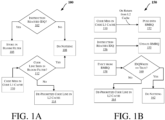
- FIGs. 1A and 1B illustrate flow diagrams of methods 100 and 150 to de-prioritize speculative code lines in on-chip caches, according to some embodiments.
- One or more of the operations of methods 100 and 150 may be performed by one or more components of FIGs. 4-8 , such as a processor, processor core, or other logic circuitry discussed herein.
- an operation 102 determines whether an instruction has reached pre-allocation or an Instruction Dispatch Queue (IDQ) 104. Once an instruction reaches IDQ at operation 102, operation 105 stores an indicia in a Bloom filter 106 (e.g., indicating that the instruction is likely to retire).
- a Bloom filter generally refers to a data/storage structure or storage unit (such as those discussed herein with reference to FIGs. 4A-8 ) used for holding state (in an embodiment, each bit in the Bloom filter denotes a block of 128B (Bytes) which reached the IDQ 104). Bloom filters are generally used to store approximate state.
- the size of a Bloom filter is relatively smaller - and hence Bloom filters are attractive to use in hardware solutions.
- the Bloom filter is 8 kB (kilo Bytes), e.g., including four tables of 2 kB each, capable of tracking 128B code regions.
- the use of four tables is part of a Bloom filter design; namely, each table may be accessed with a different hash function.
- the use of multiple hashes reduces the number of false positives in a Bloom filter.
- Method 100 performs no action at operation 108 if an instruction does not reach the IDQ 104 (e.g., indicating that the instruction is unlikely to retire).
- the Bloom filter hardware may be contained in one hardware cluster, called the front end in some processor implementations.
- the instruction(s) or micro-operations ("uops") indicia stored in the Bloom filter 106 may include the virtual address of (e.g., all) instruction(s)/uop(s) being allocated in the IDQ 104.
- the IDQ 104 is a queue where instructions/uops are stored prior to their allocation in the pre-execution stage of the processor pipeline.
- Operation 102 may be performed by logic provided in the front end 430 or execution engine 450, or logic coupled between the front end 430 and the execution engine 450 to identify a simple metric to predict whether a code line (stored in an L2 cache (such as L2 caches discussed herein, e.g., L2 cache 476 of FIG. 4B ) is speculative. For example, code lines whose instructions do not reach pre-allocation stage or the IDQ 104 are identified at operation 102, which are likely to be speculative. Generally, the IDQ 104 allows the code processing to run ahead.
- L2 cache such as L2 caches discussed herein, e.g., L2 cache 476 of FIG. 4B
- the pre-allocation stage occurs after the decode stage (e.g., decode state 406 of FIG. 4A , so the branch and target information are known at this point, or after decoding by the decode circuitry 440 in the front end 430 of FIG. 4B ), but prior to pre-scheduling/pre-allocation into a scheduler, e.g., prior to reaching the allocate stage 408 of FIG. 4A or rename/allocator circuitry 452 and scheduler(s) 456 in the execution engine 450 of FIG. 4B . Doing so before allocation is in part because the identified code line/micro-operation is considered likely to retire (e.g., by the retirement unit 454 of FIG. 4B ). Hence, the information stored in the Bloom filter 106 can be used to predict whether a code line is speculative (e.g., by assuming that code lines represented in the Bloom filter are likely to retire).
- a code miss in code L1 cache triggers operation 112 to determine whether a code line corresponding to the code miss in the L1 cache is present in the Bloom filter 106.
- operation 112 checks the Bloom filter 106 for the corresponding virtual address of the code miss. If the Bloom filter does not contain an indicia corresponding to the code miss (or otherwise a corresponding reference is absent from the Bloom filter), the code line is deemed as speculative and such speculative lines are assigned lower priority in the L2 cache at operation 114, e.g., both at the time of allocation and demand access.
- the code miss request is forwarded to the L2 cache with an indication to de-prioritize that code line in the L2 cache (e.g., with a hit in the L2 cache, the age of the code line is set to 0 (or a lowest priority value for earliest eviction from the L2 cache), and with a miss in L2 cache, an entry is inserted into the L2 cache for the code line with age 0 (or a lowest priority value for earliest eviction from the L2 cache)). Otherwise if the code line is not seen in the Bloom filter at operation 112, method 100 performs no action at operation 108.
- a miss in the Bloom filter 106 (which means that the 128B block has not been seen in IDQ 104) is a true miss - not a false negative.
- a hit in the Bloom filter 106 means that the 128B block may or may not have reached the IDQ 104 - false positives are possible.
- a false positive would, however, not hurt/reduce performance relative to current implementations, and would merely potentially reduce the performance upside of embodiments since code lines that could have been de-prioritized are not being de-prioritized.
- some embodiments use an 8KB Bloom filter that tracks code bytes at 128B granularity, as this is found to potentially reduce false positives.
- RMRQ 154 is a 16-entry queue First In First Out (FIFO) queue. Each RMRQ entry contains four fields:
- a new entry is pushed into RMRQ 154 at operation 152 when a code line is fetched from L2 cache, e.g., into an Instruction Stream Buffer (ISB, which may function in a manner similar to a code cache's MSHR (Miss Status Handling Register)). Moreover, the MSHR holds the request that missed in code L1 cache and is responsible for filling back into the code L1 cache once MSHR receives data from the L2 cache. For the oldest entry popped/evicted from RMRQ 154 at an operation 158, there are the following possibilities:
- the IDQWrite field is set to TRUE for the RMRQ entry whose VirtAddr matches the instruction's program counter.
- arbitration logic of a L2 cache controller's determines which request will arbitrate the L2 cache in a particular cycle.
- the L2 cache controller (not shown but may be coupled to and/or located on the same integrated circuit device as the L2 cache) may be modified to assign the highest priority to L2 de-prioritization requests received from the RMRQ 154.
- L2 controller arbitrates the L2 cache, and for the code line whose address matches the requested address, the priority value is set to 0 (lowest priority value for earliest eviction from the L2 cache).
- the RMRQ mechanism requires minimal hardware (e.g., 250 bytes) but its implementation may require communication between two hardware clusters - the front end 430 and the L2 cache 476.
- method 150 tracks code lines (in a queue of about 250 Bytes) returned from the L2 cache 476and whether they reach the IDQ 104.
- a (e.g., data-less) request is issued to the L2 cache to de-prioritize the identified code line in the L2 cache.
- the data-less request may include the code line address with another flag (e.g., 2 bits) to cause the age of that code line to be set to 0 (or lowest priority value for earliest eviction from the L2 cache).
- one or more embodiments are able to:
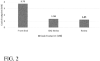
- FIG. 2 illustrates a sample average code footprint observed across stages in a processor pipeline for large code footprint workloads, according to an embodiment.
- a code line is considered non-speculative if the instructions of the code line are executed by the processor.
- FIG. 2 it can be observed that most instructions that are eventually executed by the processor reach the pre-execution stage. This can be observed by tracking unique code footprints observed at different stages in the pipeline. As shown in FIG. 2 , the unique code footprint observed at the pre-execution stage (i.e., IDQ write) is almost the same as retired/executed stage.
- this information augments one or more embodiments in the following ways: (1) instructions may reach the pre-execution stage approximately 1000+ cycles earlier than the retired stage; hence, tracking pre-execution stage results in an early indication about whether a line is speculative or not; and (2) the hardware cluster for the pre-execution stage (IDQ write) is located next to the front end, where the decision about deprioritizing code lines is made; hence, resulting in tracking pre-execution stage results in a smaller and less complicated communication channel.
- FIG. 3 illustrates the impact of proposed techniques on a suite of large code footprint workloads, according to an embodiment.
- the baseline system mimics a sample server processor.
- the proposed Bloom filter 106 and RMRQ 154 approaches improve a workload's performance (geometric mean) by about 1.8 percent and 2 percent, respectively.
- the proposed Bloom filter and RMRQ techniques improve workload performance by about 4.6% and 6.2%, respectively.
- At least one embodiment deprioritizes speculative code lines in the L2 cache by: (1) identifying a simple metric to predict if a code line is speculative or not (for example, code lines whose instructions do not reach the pre-allocation stage/IDQ are identified, which are very likely to be speculative); and (2) using the above-mentioned metric with one of two techniques to de-prioritize speculative code lines in the L2 cache. Both techniques under (2) may make minimal changes to existing hardware. Also, the above heuristic (1) enables low-hardware-cost solutions to optimize for speculative lines in at least one embodiment.
- some embodiments may be applied in computing systems that include one or more processors (e.g., where the one or more processors may include one or more processor cores), such as those discussed with reference to FIGs. 1A et seq., including for example a desktop computer, a workstation, a computer server, a server blade, or a mobile computing device.
- the mobile computing device may include a smartphone, tablet, UMPC (Ultra-Mobile Personal Computer), laptop computer, Ultrabook TM computing device, wearable devices (such as a smart watch, smart ring, smart bracelet, or smart glasses), etc.
- Processor cores may be implemented in different ways, for different purposes, and in different processors.
- implementations of such cores may include: 1) a general purpose in-order core intended for general-purpose computing; 2) a high performance general purpose out-of-order core intended for general-purpose computing; 3) a special purpose core intended primarily for graphics and/or scientific (throughput) computing.
- Implementations of different processors may include: 1) a CPU (Central Processing Unit) including one or more general purpose in-order cores intended for general-purpose computing and/or one or more general purpose out-of-order cores intended for general-purpose computing; and 2) a coprocessor including one or more special purpose cores intended primarily for graphics and/or scientific (throughput).
- CPU Central Processing Unit
- Such different processors lead to different computer system architectures, which may include: 1) the coprocessor on a separate chip from the CPU; 2) the coprocessor on a separate die in the same package as a CPU; 3) the coprocessor on the same die as a CPU (in which case, such a coprocessor is sometimes referred to as special purpose logic, such as integrated graphics and/or scientific (throughput) logic, or as special purpose cores); and 4) a system on a chip that may include on the same die the described CPU (sometimes referred to as the application core(s) or application processor(s)), the above described coprocessor, and additional functionality.
- Exemplary core architectures are described next, followed by descriptions of exemplary processors and computer architectures.
- FIG. 4A is a block diagram illustrating both an exemplary in-order pipeline and an exemplary register renaming, out-of-order issue/execution pipeline according to embodiments.
- FIG. 4B is a block diagram illustrating both an exemplary embodiment of an in-order architecture core and an exemplary register renaming, out-of-order issue/execution architecture core to be included in a processor according to embodiments.
- the solid lined boxes in FIGS. 4A-B illustrate the in-order pipeline and in-order core, while the optional addition of the dashed lined boxes illustrates the register renaming, out-of-order issue/execution pipeline and core. Given that the in-order aspect is a subset of the out-of-order aspect, the out-of-order aspect will be described.
- a processor pipeline 400 includes a fetch stage 402, a length decode stage 404, a decode stage 406, an allocation stage 408, a renaming stage 410, a scheduling (also known as a dispatch or issue) stage 412, a register read/memory read stage 414, an execute stage 416, a write back/memory write stage 418, an exception handling stage 422, and a commit stage 424.
- the core 490 includes a microcode ROM or other medium that stores microcode for certain macroinstructions (e.g., in decode unit 440 or otherwise within the front end unit 430).
- the decode unit 440 is coupled to a rename/allocator unit 452 in the execution engine unit 450.
- FIG. 6 is a block diagram of a processing system 600, according to an embodiment.
- the system 600 includes one or more processors 602 and one or more graphics processors 608, and may be a single processor desktop system, a multiprocessor workstation system, or a server system having a large number of processors 602 or processor cores 607.
- the system 600 is a processing platform incorporated within a system-on-a-chip (SoC or SOC) integrated circuit for use in mobile, handheld, or embedded devices.
- SoC system-on-a-chip
- the one or more processors 602 each include one or more processor cores 607 to process instructions which, when executed, perform operations for system and user software.
- each of the one or more processor cores 607 is configured to process a specific instruction set 609.
- instruction set 609 may facilitate Complex Instruction Set Computing (CISC), Reduced Instruction Set Computing (RISC), or computing via a Very Long Instruction Word (VLIW).
- Multiple processor cores 607 may each process a different instruction set 609, which may include instructions to facilitate the emulation of other instruction sets.
- Processor core 607 may also include other processing devices, such a Digital Signal Processor (DSP).
- DSP Digital Signal Processor
- Memory device 620 can be a dynamic random access memory (DRAM) device, a static random access memory (SRAM) device, flash memory device, phase-change memory device, or some other memory device having suitable performance to serve as process memory.
- the memory device 620 can operate as system memory for the system 600, to store data 622 and instructions 621 for use when the one or more processors 602 executes an application or process.
- Memory controller hub 616 also couples with an optional external graphics processor 612, which may communicate with the one or more graphics processors 608 in processors 602 to perform graphics and media operations.
- ICH 630 enables peripherals to connect to memory device 620 and processor 602 via a high-speed I/O bus.
- the I/O peripherals include, but are not limited to, an audio controller 646, a firmware interface 628, a wireless transceiver 626 (e.g., Wi-Fi, Bluetooth), a data storage device 624 (e.g., hard disk drive, flash memory, etc.), and a legacy I/O controller 640 for coupling legacy (e.g., Personal System 2 (PS/2)) devices to the system.
- legacy I/O controller 640 for coupling legacy (e.g., Personal System 2 (PS/2)) devices to the system.
- PS/2 Personal System 2
- USB Universal Serial Bus
- a network controller 634 may also couple to ICH 630.
- a high-performance network controller (not shown) couples to processor bus 610.
- the system 600 shown is exemplary and not limiting, as other types of data processing systems that are differently configured may also be used.
- the I/O controller hub 630 may be integrated within the one or more processor 602, or the memory controller hub 616 and I/O controller hub 630 may be integrated into a discreet external graphics processor, such as the external graphics processor 612.
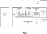
- FIG. 7 is a block diagram of an embodiment of a processor 700 having one or more processor cores 702A to 702N, an integrated memory controller 714, and an integrated graphics processor 708. Those elements of FIG. 7 having the same reference numbers (or names) as the elements of any other figure herein can operate or function in any manner similar to that described elsewhere herein, but are not limited to such.
- Processor 700 can include additional cores up to and including additional core 702N represented by the dashed lined boxes.
- Each of processor cores 702A to 702N includes one or more internal cache units 704A to 704N. In some embodiments each processor core also has access to one or more shared cached units 706.
- the internal cache units 704A to 704N and shared cache units 706 represent a cache memory hierarchy within the processor 700.
- the cache memory hierarchy may include at least one level of instruction and data cache within each processor core and one or more levels of shared mid-level cache, such as a Level 2 (L2), Level 3 (L3), Level 4 (L4), or other levels of cache, where the highest level of cache before external memory is classified as the LLC.
- cache coherency logic maintains coherency between the various cache units 706 and 704A to 704N.
- processor 700 may also include a set of one or more bus controller units 716 and a system agent core 710.
- the one or more bus controller units 716 manage a set of peripheral buses, such as one or more Peripheral Component Interconnect buses (e.g., PCI, PCI Express).
- System agent core 710 provides management functionality for the various processor components.
- system agent core 710 includes one or more integrated memory controllers 714 to manage access to various external memory devices (not shown).
- one or more of the processor cores 702A to 702N include support for simultaneous multi-threading.
- the system agent core 710 includes components for coordinating and operating cores 702A to 702N during multi-threaded processing.
- System agent core 710 may additionally include a power control unit (PCU), which includes logic and components to regulate the power state of processor cores 702A to 702N and graphics processor 708.
- PCU power control unit
- processor 700 additionally includes graphics processor 708 to execute graphics processing operations.
- the graphics processor 708 couples with the set of shared cache units 706, and the system agent core 710, including the one or more integrated memory controllers 714.
- a display controller 711 is coupled with the graphics processor 708 to drive graphics processor output to one or more coupled displays.
- display controller 711 may be a separate module coupled with the graphics processor via at least one interconnect, or may be integrated within the graphics processor 708 or system agent core 710.
- a ring based interconnect unit 712 is used to couple the internal components of the processor 700.
- an alternative interconnect unit may be used, such as a point-to-point interconnect, a switched interconnect, or other techniques, including techniques well known in the art.
- graphics processor 708 couples with the ring interconnect 712 via an I/O link 713.
- the exemplary I/O link 713 represents at least one of multiple varieties of I/O interconnects, including an on package I/O interconnect which facilitates communication between various processor components and a high-performance embedded memory module 718, such as an eDRAM (or embedded DRAM) module.
- a high-performance embedded memory module 718 such as an eDRAM (or embedded DRAM) module.
- each of the processor cores 702 to 702N and graphics processor 708 use embedded memory modules 718 as a shared Last Level Cache.
- processor cores 702A to 702N are homogenous cores executing the same instruction set architecture.
- processor cores 702A to 702N are heterogeneous in terms of instruction set architecture (ISA), where one or more of processor cores 702A to 702N execute a first instruction set, while at least one of the other cores executes a subset of the first instruction set or a different instruction set.
- processor cores 702A to 702N are heterogeneous in terms of microarchitecture, where one or more cores having a relatively higher power consumption couple with one or more power cores having a lower power consumption.
- processor 700 can be implemented on one or more chips or as an SoC integrated circuit having the illustrated components, in addition to other components.
- FIG. 8 is a block diagram of a graphics processor 800, which may be a discrete graphics processing unit, or may be a graphics processor integrated with a plurality of processing cores.
- the graphics processor communicates via a memory mapped I/O interface to registers on the graphics processor and with commands placed into the processor memory.
- graphics processor 800 includes a memory interface 814 to access memory.
- Memory interface 814 can be an interface to local memory, one or more internal caches, one or more shared external caches, and/or to system memory.
- graphics processor 800 also includes a display controller 802 to drive display output data to a display device 820.
- Display controller 802 includes hardware for one or more overlay planes for the display and composition of multiple layers of video or user interface elements.
- graphics processor 800 includes a video codec engine 806 to encode, decode, or transcode media to, from, or between one or more media encoding formats, including, but not limited to Moving Picture Experts Group (MPEG) formats such as MPEG-2, Advanced Video Coding (AVC) formats such as H.264/MPEG-4 AVC, as well as the Society of Motion Picture & Television Engineers (SMPTE) 321M/VC-1 , and Joint Photographic Experts Group (JPEG) formats such as JPEG, and Motion JPEG (MJPEG) formats.
- MPEG Moving Picture Experts Group
- AVC Advanced Video Coding
- SMPTE Society of Motion Picture & Television Engineers
- JPEG Joint Photographic Experts Group
- JPEG Joint Photographic Experts Group
- graphics processor 800 includes a block image transfer (BLIT) engine 804 to perform two-dimensional (2D) rasterizer operations including, for example, bit-boundary block transfers.
- 2D two-dimensional
- 3D graphics operations are performed using one or more components of graphics processing engine (GPE) 810.
- graphics processing engine 810 is a compute engine for performing graphics operations, including three-dimensional (3D) graphics operations and media operations.
- GPE 810 includes a 3D pipeline 812 for performing 3D operations, such as rendering three-dimensional images and scenes using processing functions that act upon 3D primitive shapes (e.g., rectangle, triangle, etc.).
- the 3D pipeline 812 includes programmable and fixed function elements that perform various tasks within the element and/or spawn execution threads to a 3D/Media sub-system 815. While 3D pipeline 812 can be used to perform media operations, an embodiment of GPE 810 also includes a media pipeline 816 that is specifically used to perform media operations, such as video post-processing and image enhancement.
- media pipeline 816 includes fixed function or programmable logic units to perform one or more specialized media operations, such as video decode acceleration, video de-interlacing, and video encode acceleration in place of, or on behalf of video codec engine 806.
- media pipeline 816 additionally includes a thread spawning unit to spawn threads for execution on 3D/Media sub-system 815. The spawned threads perform computations for the media operations on one or more graphics execution units included in 3D/Media sub-system 815.
- 3D/Media subsystem 815 includes logic for executing threads spawned by 3D pipeline 812 and media pipeline 816.
- the pipelines send thread execution requests to 3D/Media subsystem 815, which includes thread dispatch logic for arbitrating and dispatching the various requests to available thread execution resources.
- the execution resources include an array of graphics execution units to process the 3D and media threads.
- 3D/Media subsystem 815 includes one or more internal caches for thread instructions and data.
- the subsystem also includes shared memory, including registers and addressable memory, to share data between threads and to store output data.
- one or more operations discussed with reference to Figs. 1A et seq. may be performed by one or more components (interchangeably referred to herein as "logic") discussed with reference to any of the figures.
- the operations discussed herein may be implemented as hardware (e.g., logic circuitry), software, firmware, or combinations thereof, which may be provided as a computer program product, e.g., including one or more tangible (e.g., non-transitory) machine-readable or computer-readable media having stored thereon instructions (or software procedures) used to program a computer to perform a process discussed herein.
- the machine-readable medium may include a storage device such as those discussed with respect to the figures.
- Such computer-readable media may be downloaded as a computer program product, wherein the program may be transferred from a remote computer (e.g., a server) to a requesting computer (e.g., a client) by way of data signals provided in a carrier wave or other propagation medium via a communication link (e.g., a bus, a modem, or a network connection).
- a remote computer e.g., a server
- a requesting computer e.g., a client
- a communication link e.g., a bus, a modem, or a network connection
- Coupled may mean that two or more elements are in direct physical or electrical contact.
- Coupled may mean that two or more elements are in direct physical or electrical contact.
- coupled may also mean that two or more elements may not be in direct contact with each other, but may still cooperate or interact with each other.
Landscapes
- Engineering & Computer Science (AREA)
- Theoretical Computer Science (AREA)
- Physics & Mathematics (AREA)
- General Engineering & Computer Science (AREA)
- General Physics & Mathematics (AREA)
- Software Systems (AREA)
- Memory System Of A Hierarchy Structure (AREA)
- Advance Control (AREA)
Claims (3)
- Einrichtung, umfassend:einen Logikschaltkreis zum Bestimmen, ob eine Speicherstruktur eine Referenz auf eine Anforderung wegen eines fehlenden Codes enthält, bevor die Anforderung wegen eines fehlenden Codes an einen gemeinsam genutzten Cache (706) übertragen wird; undwobei der Logikschaltkreis eine Entpriorisierung einer spekulativen Codezeile, die der Anforderung wegen eines fehlenden Codes entspricht, im gemeinsam genutzten Cache als Reaktion auf das Nichtvorhandensein der Referenz in der Speicherstruktur bewirkt,wobei die Anforderung wegen eines fehlenden Codes an den gemeinsam genutzten Cache gerichtet wird;wobei die Speicherstruktur ein Bloom-Filter (106) umfasst;wobei der Logikschaltkreis die Anforderung wegen eines fehlenden Codes mit einer Angabe, die Codezeile im gemeinsam genutzten Cache als Reaktion auf das Nichtvorhandensein der Referenz in der Speicherstruktur zu entpriorisieren, an den gemeinsam genutzten Cache weiterleiten soll,wobei der gemeinsam genutzte Cache ein Level 2-Cache ;L2-Cache; (476) ist oder wobei die Anforderung wegen eines fehlenden Codes nach einem Fehlen in einem Level 1-Cache ;L1-Cache; für Code an den gemeinsam genutzten Cache gerichtet wird; undwobei die Speicherstruktur ein Zeichen einer oder mehrerer Anweisungen oder einer oder mehrerer Mikrooperationen, die in einer Instruction Dispatch Queue ;IDQ; (104) zugeordnet wurden, speichern soll oder wobei die IDQ (104) eine Anweisung oder eine Mikrooperation vor der Zuordnung in einer Vorausführungsphase einer Prozessor-Pipeline (400) speichern soll.
- Einrichtung nach Anspruch 1, wobei die Speicherstruktur eine virtuelle Adresse einer oder mehrerer Anweisungen oder einer oder mehrerer Mikrooperationen, die in einer IDQ (104) zugeordnet wurden, speichern soll oder wobei die IDQ (104) eine Anweisung oder eine Mikrooperation vor der Zuordnung in einer Vorausführungsphase einer Prozessor-Pipeline (400) speichern soll.
- Einrichtung nach Anspruch 1, wobei ein Prozessor, der einen oder mehrere Prozessorkerne aufweist, eines oder mehrere umfasst von: dem Logikschaltkreis und dem gemeinsamen Cache.
Applications Claiming Priority (1)
| Application Number | Priority Date | Filing Date | Title |
|---|---|---|---|
| US17/551,172 US12417182B2 (en) | 2021-12-14 | 2021-12-14 | De-prioritizing speculative code lines in on-chip caches |
Publications (2)
| Publication Number | Publication Date |
|---|---|
| EP4198749A1 EP4198749A1 (de) | 2023-06-21 |
| EP4198749B1 true EP4198749B1 (de) | 2024-12-11 |
Family
ID=84330348
Family Applications (1)
| Application Number | Title | Priority Date | Filing Date |
|---|---|---|---|
| EP22206038.6A Active EP4198749B1 (de) | 2021-12-14 | 2022-11-08 | Entpriorisierung spekulativer code-leitungen in on-chip-cache-speichern |
Country Status (3)
| Country | Link |
|---|---|
| US (1) | US12417182B2 (de) |
| EP (1) | EP4198749B1 (de) |
| CN (1) | CN116263671A (de) |
Families Citing this family (5)
| Publication number | Priority date | Publication date | Assignee | Title |
|---|---|---|---|---|
| US12182018B2 (en) | 2020-12-23 | 2024-12-31 | Intel Corporation | Instruction and micro-architecture support for decompression on core |
| US12242851B2 (en) | 2021-09-09 | 2025-03-04 | Intel Corporation | Verifying compressed stream fused with copy or transform operations |
| US12417182B2 (en) | 2021-12-14 | 2025-09-16 | Intel Corporation | De-prioritizing speculative code lines in on-chip caches |
| US12360768B2 (en) | 2021-12-16 | 2025-07-15 | Intel Corporation | Throttling code fetch for speculative code paths |
| CN117909092B (zh) * | 2023-12-22 | 2026-02-24 | 进迭时空(杭州)科技有限公司 | 一种优化缓存延迟的旁路访问方法及系统 |
Family Cites Families (88)
| Publication number | Priority date | Publication date | Assignee | Title |
|---|---|---|---|---|
| US5809268A (en) | 1995-06-29 | 1998-09-15 | International Business Machines Corporation | Method and system for tracking resource allocation within a processor |
| JPH0922353A (ja) | 1995-07-05 | 1997-01-21 | Toshiba Corp | 1チップ・マイクロコンピュータおよびその命令コード格納方法 |
| US5699537A (en) | 1995-12-22 | 1997-12-16 | Intel Corporation | Processor microarchitecture for efficient dynamic scheduling and execution of chains of dependent instructions |
| US6049866A (en) | 1996-09-06 | 2000-04-11 | Silicon Graphics, Inc. | Method and system for an efficient user mode cache manipulation using a simulated instruction |
| US6879266B1 (en) | 1997-08-08 | 2005-04-12 | Quickshift, Inc. | Memory module including scalable embedded parallel data compression and decompression engines |
| US6388585B1 (en) | 1998-08-11 | 2002-05-14 | Matsushita Electric Industrial Co Ltd | Method for data compression and decompression using decompression instructions |
| US6233645B1 (en) | 1998-11-02 | 2001-05-15 | Compaq Computer Corporation | Dynamically disabling speculative prefetch when high priority demand fetch opportunity use is high |
| US6208273B1 (en) | 1999-01-29 | 2001-03-27 | Interactive Silicon, Inc. | System and method for performing scalable embedded parallel data compression |
| US6505293B1 (en) | 1999-07-07 | 2003-01-07 | Intel Corporation | Register renaming to optimize identical register values |
| US6625723B1 (en) | 1999-07-07 | 2003-09-23 | Intel Corporation | Unified renaming scheme for load and store instructions |
| US6446145B1 (en) | 2000-01-06 | 2002-09-03 | International Business Machines Corporation | Computer memory compression abort and bypass mechanism when cache write back buffer is full |
| US6862662B1 (en) | 2000-03-03 | 2005-03-01 | Micron Technology, Inc. | High density storage scheme for semiconductor memory |
| US7287649B2 (en) | 2001-05-18 | 2007-10-30 | Broadcom Corporation | System on a chip for packet processing |
| US7051195B2 (en) | 2001-10-26 | 2006-05-23 | Hewlett-Packard Development Company, L.P. | Method of optimization of CPU and chipset performance by support of optional reads by CPU and chipset |
| US7114059B2 (en) | 2001-11-05 | 2006-09-26 | Intel Corporation | System and method to bypass execution of instructions involving unreliable data during speculative execution |
| US7181598B2 (en) | 2002-05-17 | 2007-02-20 | Intel Corporation | Prediction of load-store dependencies in a processing agent |
| US6934865B2 (en) | 2002-07-09 | 2005-08-23 | University Of Massachusetts | Controlling a processor resource based on a compile-time prediction of number of instructions-per-cycle that will be executed across plural cycles by the processor |
| US6976131B2 (en) * | 2002-08-23 | 2005-12-13 | Intel Corporation | Method and apparatus for shared cache coherency for a chip multiprocessor or multiprocessor system |
| US7257693B2 (en) | 2004-01-15 | 2007-08-14 | Intel Corporation | Multi-processor computing system that employs compressed cache lines' worth of information and processor capable of use in said system |
| US20050289300A1 (en) | 2004-06-24 | 2005-12-29 | International Business Machines Corporation | Disable write back on atomic reserved line in a small cache system |
| US7519796B1 (en) | 2004-06-30 | 2009-04-14 | Sun Microsystems, Inc. | Efficient utilization of a store buffer using counters |
| US7392366B2 (en) | 2004-09-17 | 2008-06-24 | International Business Machines Corp. | Adaptive fetch gating in multithreaded processors, fetch control and method of controlling fetches |
| US7548908B2 (en) * | 2005-06-24 | 2009-06-16 | Yahoo! Inc. | Dynamic bloom filter for caching query results |
| US20080282034A1 (en) | 2005-09-19 | 2008-11-13 | Via Technologies, Inc. | Memory Subsystem having a Multipurpose Cache for a Stream Graphics Multiprocessor |
| US7721071B2 (en) | 2006-02-28 | 2010-05-18 | Mips Technologies, Inc. | System and method for propagating operand availability prediction bits with instructions through a pipeline in an out-of-order processor |
| US8032734B2 (en) | 2006-09-06 | 2011-10-04 | Mips Technologies, Inc. | Coprocessor load data queue for interfacing an out-of-order execution unit with an in-order coprocessor |
| US7925868B2 (en) | 2007-01-24 | 2011-04-12 | Arm Limited | Suppressing register renaming for conditional instructions predicted as not executed |
| US7627742B2 (en) | 2007-04-10 | 2009-12-01 | International Business Machines Corporation | Method and apparatus for conserving power by throttling instruction fetching when a processor encounters low confidence branches in an information handling system |
| US8006073B1 (en) | 2007-09-28 | 2011-08-23 | Oracle America, Inc. | Simultaneous speculative threading light mode |
| US20100223237A1 (en) | 2007-11-05 | 2010-09-02 | University Of Florida Research Foundation, Inc. | Lossless data compression and real-time decompression |
| US8006070B2 (en) | 2007-12-05 | 2011-08-23 | International Business Machines Corporation | Method and apparatus for inhibiting fetch throttling when a processor encounters a low confidence branch instruction in an information handling system |
| US8447948B1 (en) | 2008-04-25 | 2013-05-21 | Amazon Technologies, Inc | Dynamic selective cache compression |
| US9639479B2 (en) | 2009-09-23 | 2017-05-02 | Nvidia Corporation | Instructions for managing a parallel cache hierarchy |
| US8914617B2 (en) | 2009-12-26 | 2014-12-16 | Intel Corporation | Tracking mechanism coupled to retirement in reorder buffer for indicating sharing logical registers of physical register in record indexed by logical register |
| US8627044B2 (en) | 2010-10-06 | 2014-01-07 | Oracle International Corporation | Issuing instructions with unresolved data dependencies |
| WO2012051281A2 (en) | 2010-10-12 | 2012-04-19 | Soft Machines, Inc. | An instruction sequence buffer to store branches having reliably predictable instruction sequences |
| US8738860B1 (en) | 2010-10-25 | 2014-05-27 | Tilera Corporation | Computing in parallel processing environments |
| JP5879527B2 (ja) | 2011-05-25 | 2016-03-08 | パナソニックIpマネジメント株式会社 | 情報処理装置および情報処理方法 |
| US9459866B2 (en) | 2011-12-30 | 2016-10-04 | Intel Corporation | Vector frequency compress instruction |
| US9367323B2 (en) | 2012-06-15 | 2016-06-14 | International Business Machines Corporation | Processor assist facility |
| US20140095814A1 (en) | 2012-09-28 | 2014-04-03 | Morris Marden | Memory Renaming Mechanism in Microarchitecture |
| US9547594B2 (en) | 2013-03-15 | 2017-01-17 | Intel Corporation | Instructions to mark beginning and end of non transactional code region requiring write back to persistent storage |
| GB2515076B (en) | 2013-06-13 | 2020-07-15 | Advanced Risc Mach Ltd | A data processing apparatus and method for handling retrieval of instructions from an instruction cache |
| WO2015057828A1 (en) | 2013-10-15 | 2015-04-23 | Mill Computing, Inc. | Computer processor employing cache memory storing backless cache lines |
| US9471494B2 (en) | 2013-12-20 | 2016-10-18 | Intel Corporation | Method and apparatus for cache line write back operation |
| US9292449B2 (en) | 2013-12-20 | 2016-03-22 | Intel Corporation | Cache memory data compression and decompression |
| CN103810297B (zh) | 2014-03-07 | 2017-02-01 | 华为技术有限公司 | 基于重删技术的写方法、读方法、写装置和读装置 |
| US10409763B2 (en) | 2014-06-30 | 2019-09-10 | Intel Corporation | Apparatus and method for efficiently implementing a processor pipeline |
| US9405706B2 (en) | 2014-09-25 | 2016-08-02 | Intel Corporation | Instruction and logic for adaptive dataset priorities in processor caches |
| GB2533768B (en) | 2014-12-19 | 2021-07-21 | Advanced Risc Mach Ltd | Cleaning a write-back cache |
| US9513919B2 (en) | 2015-04-28 | 2016-12-06 | Intel Corporation | Method and apparatus for speculative decompression |
| US10705964B2 (en) | 2015-04-28 | 2020-07-07 | Intel Corporation | Controlling displacement in a co-operative and adaptive multiple-level memory system |
| US9552169B2 (en) | 2015-05-07 | 2017-01-24 | Intel Corporation | Apparatus and method for efficient memory renaming prediction using virtual registers |
| US20170046164A1 (en) | 2015-08-14 | 2017-02-16 | Qualcomm Incorporated | High performance recovery from misspeculation of load latency |
| US9928068B2 (en) | 2015-12-07 | 2018-03-27 | International Business Machines Corporation | Hardware managed dynamic thread fetch rate control |
| US10296463B2 (en) | 2016-01-07 | 2019-05-21 | Samsung Electronics Co., Ltd. | Instruction prefetcher dynamically controlled by readily available prefetcher accuracy |
| US9836405B2 (en) | 2016-01-29 | 2017-12-05 | International Business Machines Corporation | Dynamic management of virtual memory blocks exempted from cache memory access |
| GB2547189A (en) | 2016-02-03 | 2017-08-16 | Swarm64 As | Cache and method |
| US10474462B2 (en) | 2016-02-29 | 2019-11-12 | Qualcomm Incorporated | Dynamic pipeline throttling using confidence-based weighting of in-flight branch instructions |
| US20170371660A1 (en) | 2016-06-23 | 2017-12-28 | Microsoft Technology Licensing, Llc | Load-store queue for multiple processor cores |
| US10002081B2 (en) | 2016-07-05 | 2018-06-19 | Intel Corporation | Apparatus for hardware implementation of heterogeneous decompression processing |
| US20180150256A1 (en) | 2016-11-29 | 2018-05-31 | Intel Corporation | Technologies for data deduplication in disaggregated architectures |
| US20180165097A1 (en) | 2016-12-14 | 2018-06-14 | Palo Alto Research Center Incorporated | Dispatch of processor read results |
| US10875435B1 (en) | 2017-03-30 | 2020-12-29 | Zoox, Inc. | Headrest with passenger flaps |
| WO2019005105A1 (en) | 2017-06-30 | 2019-01-03 | Intel Corporation | ACTIVATION OF SPECULATIVE MEMORY |
| US10331558B2 (en) | 2017-07-28 | 2019-06-25 | Apple Inc. | Systems and methods for performing memory compression |
| US10954674B2 (en) | 2018-05-08 | 2021-03-23 | Gregory A. Header | Heated snow guard |
| US10691529B2 (en) | 2018-06-20 | 2020-06-23 | Intel Corporation | Supporting random access of compressed data |
| US11258704B2 (en) | 2018-06-29 | 2022-02-22 | Intel Corporation | Technologies for managing network traffic through heterogeneous networks |
| US10936404B2 (en) | 2018-06-30 | 2021-03-02 | Intel Corporation | Technologies for error detection in compressed data streams |
| US10671550B1 (en) | 2019-01-03 | 2020-06-02 | International Business Machines Corporation | Memory offloading a problem using accelerators |
| US10831497B2 (en) | 2019-01-31 | 2020-11-10 | International Business Machines Corporation | Compression/decompression instruction specifying a history buffer to be used in the compression/decompression of data |
| US11681533B2 (en) | 2019-02-25 | 2023-06-20 | Intel Corporation | Restricted speculative execution mode to prevent observable side effects |
| KR20210136994A (ko) | 2019-03-15 | 2021-11-17 | 인텔 코포레이션 | 매트릭스 가속기 아키텍처 내에서의 시스톨릭 분리 |
| CN113439265A (zh) | 2019-03-15 | 2021-09-24 | 英特尔公司 | 用于更新多gpu配置中的存储器侧高速缓存的系统和方法 |
| US11086625B2 (en) | 2019-09-10 | 2021-08-10 | Apple Inc. | Compression assist instructions |
| US11809902B2 (en) | 2020-09-24 | 2023-11-07 | Advanced Micro Devices, Inc. | Fine-grained conditional dispatching |
| US12066945B2 (en) | 2020-12-22 | 2024-08-20 | Intel Corporation | Dynamic shared cache partition for workload with large code footprint |
| US12182018B2 (en) | 2020-12-23 | 2024-12-31 | Intel Corporation | Instruction and micro-architecture support for decompression on core |
| US12028094B2 (en) | 2020-12-23 | 2024-07-02 | Intel Corporation | Application programming interface for fine grained low latency decompression within processor core |
| US20220197813A1 (en) | 2020-12-23 | 2022-06-23 | Intel Corporation | Application programming interface for fine grained low latency decompression within processor core |
| US20220197643A1 (en) | 2020-12-23 | 2022-06-23 | Intel Corporation | Speculative decompression within processor core caches |
| US11889348B2 (en) | 2021-02-19 | 2024-01-30 | Qualcomm Incorporated | Techniques for compressing feedback values in wireless communications |
| US11576078B2 (en) | 2021-03-15 | 2023-02-07 | International Business Machines Corporation | Selective compression of data for uplink to a telecommunication network |
| WO2023287533A1 (en) | 2021-07-13 | 2023-01-19 | SiFive, Inc. | Processor power management using instruction throttling |
| US12242851B2 (en) | 2021-09-09 | 2025-03-04 | Intel Corporation | Verifying compressed stream fused with copy or transform operations |
| US11625349B1 (en) | 2021-11-18 | 2023-04-11 | Arm Limited | Apparatus and method for managing prefetch transactions |
| US12417182B2 (en) | 2021-12-14 | 2025-09-16 | Intel Corporation | De-prioritizing speculative code lines in on-chip caches |
-
2021
- 2021-12-14 US US17/551,172 patent/US12417182B2/en active Active
-
2022
- 2022-10-27 CN CN202211329988.7A patent/CN116263671A/zh active Pending
- 2022-11-08 EP EP22206038.6A patent/EP4198749B1/de active Active
Also Published As
| Publication number | Publication date |
|---|---|
| CN116263671A (zh) | 2023-06-16 |
| US12417182B2 (en) | 2025-09-16 |
| EP4198749A1 (de) | 2023-06-21 |
| US20230185718A1 (en) | 2023-06-15 |
Similar Documents
| Publication | Publication Date | Title |
|---|---|---|
| US12417182B2 (en) | De-prioritizing speculative code lines in on-chip caches | |
| US11436695B2 (en) | Coarse grain coherency | |
| EP4209915B1 (de) | Registerdateivorausholen | |
| EP4152167A1 (de) | Skalierbares adressdecodierschema für cxl typ-2 geräte mit programmierbarer verschachtelungsgranularität | |
| EP4020230B1 (de) | Anwendungsprogrammierungsschnittstelle für feinkörnige niedriglatente dekomprimierung im prozessorkern | |
| US12455701B2 (en) | Scalable access control checking for cross-address-space data movement | |
| US20250117329A1 (en) | Instruction and Micro-Architecture Support for Decompression on Core | |
| US20230091205A1 (en) | Memory side prefetch architecture for improved memory bandwidth | |
| EP4020231B1 (de) | Spekulative dekomprimierung in prozessorkern-cachespeichern | |
| US11928472B2 (en) | Branch prefetch mechanisms for mitigating frontend branch resteers | |
| EP4020223B1 (de) | Erhöhung der speicherbandbreite pro kern unter verwendung von vergessensspeichern | |
| WO2023173276A1 (en) | Universal core to accelerator communication architecture | |
| US20170322887A1 (en) | Method to control cache replacement for decoupled data fetch | |
| US12360768B2 (en) | Throttling code fetch for speculative code paths | |
| CN121681410A (zh) | 用于许多核处理器中改善的数据共享的被延迟高速缓存写回指令 | |
| US20240220410A1 (en) | Leveraging System Cache for Performance Cores |
Legal Events
| Date | Code | Title | Description |
|---|---|---|---|
| PUAI | Public reference made under article 153(3) epc to a published international application that has entered the european phase |
Free format text: ORIGINAL CODE: 0009012 |
|
| STAA | Information on the status of an ep patent application or granted ep patent |
Free format text: STATUS: THE APPLICATION HAS BEEN PUBLISHED |
|
| AK | Designated contracting states |
Kind code of ref document: A1 Designated state(s): AL AT BE BG CH CY CZ DE DK EE ES FI FR GB GR HR HU IE IS IT LI LT LU LV MC ME MK MT NL NO PL PT RO RS SE SI SK SM TR |
|
| STAA | Information on the status of an ep patent application or granted ep patent |
Free format text: STATUS: REQUEST FOR EXAMINATION WAS MADE |
|
| REG | Reference to a national code |
Ref country code: DE Ref legal event code: R079 Free format text: PREVIOUS MAIN CLASS: G06F0012089700 Ipc: G06F0012087500 Ref document number: 602022008588 Country of ref document: DE |
|
| 17P | Request for examination filed |
Effective date: 20231218 |
|
| RBV | Designated contracting states (corrected) |
Designated state(s): AL AT BE BG CH CY CZ DE DK EE ES FI FR GB GR HR HU IE IS IT LI LT LU LV MC ME MK MT NL NO PL PT RO RS SE SI SK SM TR |
|
| RIC1 | Information provided on ipc code assigned before grant |
Ipc: G06F 12/126 20160101ALI20240116BHEP Ipc: G06F 9/38 20180101ALI20240116BHEP Ipc: G06F 12/0897 20160101ALI20240116BHEP Ipc: G06F 12/0875 20160101AFI20240116BHEP |
|
| STAA | Information on the status of an ep patent application or granted ep patent |
Free format text: STATUS: EXAMINATION IS IN PROGRESS |
|
| 17Q | First examination report despatched |
Effective date: 20240221 |
|
| GRAP | Despatch of communication of intention to grant a patent |
Free format text: ORIGINAL CODE: EPIDOSNIGR1 |
|
| STAA | Information on the status of an ep patent application or granted ep patent |
Free format text: STATUS: GRANT OF PATENT IS INTENDED |
|
| INTG | Intention to grant announced |
Effective date: 20240708 |
|
| GRAS | Grant fee paid |
Free format text: ORIGINAL CODE: EPIDOSNIGR3 |
|
| GRAA | (expected) grant |
Free format text: ORIGINAL CODE: 0009210 |
|
| STAA | Information on the status of an ep patent application or granted ep patent |
Free format text: STATUS: THE PATENT HAS BEEN GRANTED |
|
| AK | Designated contracting states |
Kind code of ref document: B1 Designated state(s): AL AT BE BG CH CY CZ DE DK EE ES FI FR GB GR HR HU IE IS IT LI LT LU LV MC ME MK MT NL NO PL PT RO RS SE SI SK SM TR |
|
| REG | Reference to a national code |
Ref country code: GB Ref legal event code: FG4D |
|
| REG | Reference to a national code |
Ref country code: CH Ref legal event code: EP |
|
| REG | Reference to a national code |
Ref country code: DE Ref legal event code: R096 Ref document number: 602022008588 Country of ref document: DE |
|
| REG | Reference to a national code |
Ref country code: IE Ref legal event code: FG4D |
|
| P01 | Opt-out of the competence of the unified patent court (upc) registered |
Free format text: CASE NUMBER: APP_65900/2024 Effective date: 20241213 |
|
| REG | Reference to a national code |
Ref country code: NL Ref legal event code: FP |
|
| REG | Reference to a national code |
Ref country code: LT Ref legal event code: MG9D |
|
| PG25 | Lapsed in a contracting state [announced via postgrant information from national office to epo] |
Ref country code: HR Free format text: LAPSE BECAUSE OF FAILURE TO SUBMIT A TRANSLATION OF THE DESCRIPTION OR TO PAY THE FEE WITHIN THE PRESCRIBED TIME-LIMIT Effective date: 20241211 |
|
| PG25 | Lapsed in a contracting state [announced via postgrant information from national office to epo] |
Ref country code: FI Free format text: LAPSE BECAUSE OF FAILURE TO SUBMIT A TRANSLATION OF THE DESCRIPTION OR TO PAY THE FEE WITHIN THE PRESCRIBED TIME-LIMIT Effective date: 20241211 |
|
| PG25 | Lapsed in a contracting state [announced via postgrant information from national office to epo] |
Ref country code: BG Free format text: LAPSE BECAUSE OF FAILURE TO SUBMIT A TRANSLATION OF THE DESCRIPTION OR TO PAY THE FEE WITHIN THE PRESCRIBED TIME-LIMIT Effective date: 20241211 |
|
| PG25 | Lapsed in a contracting state [announced via postgrant information from national office to epo] |
Ref country code: ES Free format text: LAPSE BECAUSE OF FAILURE TO SUBMIT A TRANSLATION OF THE DESCRIPTION OR TO PAY THE FEE WITHIN THE PRESCRIBED TIME-LIMIT Effective date: 20241211 |
|
| PG25 | Lapsed in a contracting state [announced via postgrant information from national office to epo] |
Ref country code: NO Free format text: LAPSE BECAUSE OF FAILURE TO SUBMIT A TRANSLATION OF THE DESCRIPTION OR TO PAY THE FEE WITHIN THE PRESCRIBED TIME-LIMIT Effective date: 20250311 |
|
| PG25 | Lapsed in a contracting state [announced via postgrant information from national office to epo] |
Ref country code: LV Free format text: LAPSE BECAUSE OF FAILURE TO SUBMIT A TRANSLATION OF THE DESCRIPTION OR TO PAY THE FEE WITHIN THE PRESCRIBED TIME-LIMIT Effective date: 20241211 Ref country code: GR Free format text: LAPSE BECAUSE OF FAILURE TO SUBMIT A TRANSLATION OF THE DESCRIPTION OR TO PAY THE FEE WITHIN THE PRESCRIBED TIME-LIMIT Effective date: 20250312 |
|
| PG25 | Lapsed in a contracting state [announced via postgrant information from national office to epo] |
Ref country code: RS Free format text: LAPSE BECAUSE OF FAILURE TO SUBMIT A TRANSLATION OF THE DESCRIPTION OR TO PAY THE FEE WITHIN THE PRESCRIBED TIME-LIMIT Effective date: 20250311 |
|
| REG | Reference to a national code |
Ref country code: AT Ref legal event code: MK05 Ref document number: 1750943 Country of ref document: AT Kind code of ref document: T Effective date: 20241211 |
|
| PG25 | Lapsed in a contracting state [announced via postgrant information from national office to epo] |
Ref country code: SM Free format text: LAPSE BECAUSE OF FAILURE TO SUBMIT A TRANSLATION OF THE DESCRIPTION OR TO PAY THE FEE WITHIN THE PRESCRIBED TIME-LIMIT Effective date: 20241211 |
|
| PG25 | Lapsed in a contracting state [announced via postgrant information from national office to epo] |
Ref country code: PL Free format text: LAPSE BECAUSE OF FAILURE TO SUBMIT A TRANSLATION OF THE DESCRIPTION OR TO PAY THE FEE WITHIN THE PRESCRIBED TIME-LIMIT Effective date: 20241211 |
|
| PG25 | Lapsed in a contracting state [announced via postgrant information from national office to epo] |
Ref country code: IS Free format text: LAPSE BECAUSE OF FAILURE TO SUBMIT A TRANSLATION OF THE DESCRIPTION OR TO PAY THE FEE WITHIN THE PRESCRIBED TIME-LIMIT Effective date: 20250411 |
|
| PG25 | Lapsed in a contracting state [announced via postgrant information from national office to epo] |
Ref country code: PT Free format text: LAPSE BECAUSE OF FAILURE TO SUBMIT A TRANSLATION OF THE DESCRIPTION OR TO PAY THE FEE WITHIN THE PRESCRIBED TIME-LIMIT Effective date: 20250411 |
|
| PG25 | Lapsed in a contracting state [announced via postgrant information from national office to epo] |
Ref country code: EE Free format text: LAPSE BECAUSE OF FAILURE TO SUBMIT A TRANSLATION OF THE DESCRIPTION OR TO PAY THE FEE WITHIN THE PRESCRIBED TIME-LIMIT Effective date: 20241211 |
|
| PG25 | Lapsed in a contracting state [announced via postgrant information from national office to epo] |
Ref country code: RO Free format text: LAPSE BECAUSE OF FAILURE TO SUBMIT A TRANSLATION OF THE DESCRIPTION OR TO PAY THE FEE WITHIN THE PRESCRIBED TIME-LIMIT Effective date: 20241211 Ref country code: AT Free format text: LAPSE BECAUSE OF FAILURE TO SUBMIT A TRANSLATION OF THE DESCRIPTION OR TO PAY THE FEE WITHIN THE PRESCRIBED TIME-LIMIT Effective date: 20241211 |
|
| PG25 | Lapsed in a contracting state [announced via postgrant information from national office to epo] |
Ref country code: SK Free format text: LAPSE BECAUSE OF FAILURE TO SUBMIT A TRANSLATION OF THE DESCRIPTION OR TO PAY THE FEE WITHIN THE PRESCRIBED TIME-LIMIT Effective date: 20241211 |
|
| PG25 | Lapsed in a contracting state [announced via postgrant information from national office to epo] |
Ref country code: CZ Free format text: LAPSE BECAUSE OF FAILURE TO SUBMIT A TRANSLATION OF THE DESCRIPTION OR TO PAY THE FEE WITHIN THE PRESCRIBED TIME-LIMIT Effective date: 20241211 |
|
| PG25 | Lapsed in a contracting state [announced via postgrant information from national office to epo] |
Ref country code: IT Free format text: LAPSE BECAUSE OF FAILURE TO SUBMIT A TRANSLATION OF THE DESCRIPTION OR TO PAY THE FEE WITHIN THE PRESCRIBED TIME-LIMIT Effective date: 20241211 |
|
| PG25 | Lapsed in a contracting state [announced via postgrant information from national office to epo] |
Ref country code: SE Free format text: LAPSE BECAUSE OF FAILURE TO SUBMIT A TRANSLATION OF THE DESCRIPTION OR TO PAY THE FEE WITHIN THE PRESCRIBED TIME-LIMIT Effective date: 20241211 |
|
| REG | Reference to a national code |
Ref country code: DE Ref legal event code: R097 Ref document number: 602022008588 Country of ref document: DE |
|
| PG25 | Lapsed in a contracting state [announced via postgrant information from national office to epo] |
Ref country code: DK Free format text: LAPSE BECAUSE OF FAILURE TO SUBMIT A TRANSLATION OF THE DESCRIPTION OR TO PAY THE FEE WITHIN THE PRESCRIBED TIME-LIMIT Effective date: 20241211 |
|
| PLBE | No opposition filed within time limit |
Free format text: ORIGINAL CODE: 0009261 |
|
| STAA | Information on the status of an ep patent application or granted ep patent |
Free format text: STATUS: NO OPPOSITION FILED WITHIN TIME LIMIT |
|
| PGFP | Annual fee paid to national office [announced via postgrant information from national office to epo] |
Ref country code: NL Payment date: 20251024 Year of fee payment: 4 |
|
| 26N | No opposition filed |
Effective date: 20250912 |
|
| PGFP | Annual fee paid to national office [announced via postgrant information from national office to epo] |
Ref country code: DE Payment date: 20250923 Year of fee payment: 4 |
|
| PGFP | Annual fee paid to national office [announced via postgrant information from national office to epo] |
Ref country code: FR Payment date: 20251023 Year of fee payment: 4 |