EP4198620A1 - Display device - Google Patents
Display device Download PDFInfo
- Publication number
- EP4198620A1 EP4198620A1 EP20880380.9A EP20880380A EP4198620A1 EP 4198620 A1 EP4198620 A1 EP 4198620A1 EP 20880380 A EP20880380 A EP 20880380A EP 4198620 A1 EP4198620 A1 EP 4198620A1
- Authority
- EP
- European Patent Office
- Prior art keywords
- disposed
- substrate
- display device
- ink layer
- layer
- Prior art date
- Legal status (The legal status is an assumption and is not a legal conclusion. Google has not performed a legal analysis and makes no representation as to the accuracy of the status listed.)
- Granted
Links
Images

Classifications
-
- G—PHYSICS
- G02—OPTICS
- G02F—OPTICAL DEVICES OR ARRANGEMENTS FOR THE CONTROL OF LIGHT BY MODIFICATION OF THE OPTICAL PROPERTIES OF THE MEDIA OF THE ELEMENTS INVOLVED THEREIN; NON-LINEAR OPTICS; FREQUENCY-CHANGING OF LIGHT; OPTICAL LOGIC ELEMENTS; OPTICAL ANALOGUE/DIGITAL CONVERTERS
- G02F1/00—Devices or arrangements for the control of the intensity, colour, phase, polarisation or direction of light arriving from an independent light source, e.g. switching, gating or modulating; Non-linear optics
- G02F1/01—Devices or arrangements for the control of the intensity, colour, phase, polarisation or direction of light arriving from an independent light source, e.g. switching, gating or modulating; Non-linear optics for the control of the intensity, phase, polarisation or colour
- G02F1/13—Devices or arrangements for the control of the intensity, colour, phase, polarisation or direction of light arriving from an independent light source, e.g. switching, gating or modulating; Non-linear optics for the control of the intensity, phase, polarisation or colour based on liquid crystals, e.g. single liquid crystal display cells
- G02F1/133—Constructional arrangements; Operation of liquid crystal cells; Circuit arrangements
- G02F1/1333—Constructional arrangements; Manufacturing methods
- G02F1/133308—Support structures for LCD panels, e.g. frames or bezels
-
- G—PHYSICS
- G02—OPTICS
- G02F—OPTICAL DEVICES OR ARRANGEMENTS FOR THE CONTROL OF LIGHT BY MODIFICATION OF THE OPTICAL PROPERTIES OF THE MEDIA OF THE ELEMENTS INVOLVED THEREIN; NON-LINEAR OPTICS; FREQUENCY-CHANGING OF LIGHT; OPTICAL LOGIC ELEMENTS; OPTICAL ANALOGUE/DIGITAL CONVERTERS
- G02F1/00—Devices or arrangements for the control of the intensity, colour, phase, polarisation or direction of light arriving from an independent light source, e.g. switching, gating or modulating; Non-linear optics
- G02F1/01—Devices or arrangements for the control of the intensity, colour, phase, polarisation or direction of light arriving from an independent light source, e.g. switching, gating or modulating; Non-linear optics for the control of the intensity, phase, polarisation or colour
- G02F1/13—Devices or arrangements for the control of the intensity, colour, phase, polarisation or direction of light arriving from an independent light source, e.g. switching, gating or modulating; Non-linear optics for the control of the intensity, phase, polarisation or colour based on liquid crystals, e.g. single liquid crystal display cells
- G02F1/133—Constructional arrangements; Operation of liquid crystal cells; Circuit arrangements
- G02F1/1333—Constructional arrangements; Manufacturing methods
- G02F1/133308—Support structures for LCD panels, e.g. frames or bezels
- G02F1/133317—Intermediate frames, e.g. between backlight housing and front frame
-
- G—PHYSICS
- G02—OPTICS
- G02B—OPTICAL ELEMENTS, SYSTEMS OR APPARATUS
- G02B6/00—Light guides; Structural details of arrangements comprising light guides and other optical elements, e.g. couplings
- G02B6/0001—Light guides; Structural details of arrangements comprising light guides and other optical elements, e.g. couplings specially adapted for lighting devices or systems
- G02B6/0011—Light guides; Structural details of arrangements comprising light guides and other optical elements, e.g. couplings specially adapted for lighting devices or systems the light guides being planar or of plate-like form
- G02B6/0081—Mechanical or electrical aspects of the light guide and light source in the lighting device peculiar to the adaptation to planar light guides, e.g. concerning packaging
- G02B6/0086—Positioning aspects
- G02B6/0088—Positioning aspects of the light guide or other optical sheets in the package
-
- G—PHYSICS
- G02—OPTICS
- G02B—OPTICAL ELEMENTS, SYSTEMS OR APPARATUS
- G02B6/00—Light guides; Structural details of arrangements comprising light guides and other optical elements, e.g. couplings
- G02B6/0001—Light guides; Structural details of arrangements comprising light guides and other optical elements, e.g. couplings specially adapted for lighting devices or systems
- G02B6/0011—Light guides; Structural details of arrangements comprising light guides and other optical elements, e.g. couplings specially adapted for lighting devices or systems the light guides being planar or of plate-like form
- G02B6/0081—Mechanical or electrical aspects of the light guide and light source in the lighting device peculiar to the adaptation to planar light guides, e.g. concerning packaging
- G02B6/0086—Positioning aspects
- G02B6/009—Positioning aspects of the light source in the package
-
- G—PHYSICS
- G02—OPTICS
- G02F—OPTICAL DEVICES OR ARRANGEMENTS FOR THE CONTROL OF LIGHT BY MODIFICATION OF THE OPTICAL PROPERTIES OF THE MEDIA OF THE ELEMENTS INVOLVED THEREIN; NON-LINEAR OPTICS; FREQUENCY-CHANGING OF LIGHT; OPTICAL LOGIC ELEMENTS; OPTICAL ANALOGUE/DIGITAL CONVERTERS
- G02F1/00—Devices or arrangements for the control of the intensity, colour, phase, polarisation or direction of light arriving from an independent light source, e.g. switching, gating or modulating; Non-linear optics
- G02F1/01—Devices or arrangements for the control of the intensity, colour, phase, polarisation or direction of light arriving from an independent light source, e.g. switching, gating or modulating; Non-linear optics for the control of the intensity, phase, polarisation or colour
- G02F1/13—Devices or arrangements for the control of the intensity, colour, phase, polarisation or direction of light arriving from an independent light source, e.g. switching, gating or modulating; Non-linear optics for the control of the intensity, phase, polarisation or colour based on liquid crystals, e.g. single liquid crystal display cells
- G02F1/133—Constructional arrangements; Operation of liquid crystal cells; Circuit arrangements
- G02F1/1333—Constructional arrangements; Manufacturing methods
-
- G—PHYSICS
- G02—OPTICS
- G02F—OPTICAL DEVICES OR ARRANGEMENTS FOR THE CONTROL OF LIGHT BY MODIFICATION OF THE OPTICAL PROPERTIES OF THE MEDIA OF THE ELEMENTS INVOLVED THEREIN; NON-LINEAR OPTICS; FREQUENCY-CHANGING OF LIGHT; OPTICAL LOGIC ELEMENTS; OPTICAL ANALOGUE/DIGITAL CONVERTERS
- G02F1/00—Devices or arrangements for the control of the intensity, colour, phase, polarisation or direction of light arriving from an independent light source, e.g. switching, gating or modulating; Non-linear optics
- G02F1/01—Devices or arrangements for the control of the intensity, colour, phase, polarisation or direction of light arriving from an independent light source, e.g. switching, gating or modulating; Non-linear optics for the control of the intensity, phase, polarisation or colour
- G02F1/13—Devices or arrangements for the control of the intensity, colour, phase, polarisation or direction of light arriving from an independent light source, e.g. switching, gating or modulating; Non-linear optics for the control of the intensity, phase, polarisation or colour based on liquid crystals, e.g. single liquid crystal display cells
- G02F1/133—Constructional arrangements; Operation of liquid crystal cells; Circuit arrangements
- G02F1/1333—Constructional arrangements; Manufacturing methods
- G02F1/133308—Support structures for LCD panels, e.g. frames or bezels
- G02F1/133311—Environmental protection, e.g. against dust or humidity
-
- G—PHYSICS
- G02—OPTICS
- G02F—OPTICAL DEVICES OR ARRANGEMENTS FOR THE CONTROL OF LIGHT BY MODIFICATION OF THE OPTICAL PROPERTIES OF THE MEDIA OF THE ELEMENTS INVOLVED THEREIN; NON-LINEAR OPTICS; FREQUENCY-CHANGING OF LIGHT; OPTICAL LOGIC ELEMENTS; OPTICAL ANALOGUE/DIGITAL CONVERTERS
- G02F1/00—Devices or arrangements for the control of the intensity, colour, phase, polarisation or direction of light arriving from an independent light source, e.g. switching, gating or modulating; Non-linear optics
- G02F1/01—Devices or arrangements for the control of the intensity, colour, phase, polarisation or direction of light arriving from an independent light source, e.g. switching, gating or modulating; Non-linear optics for the control of the intensity, phase, polarisation or colour
- G02F1/13—Devices or arrangements for the control of the intensity, colour, phase, polarisation or direction of light arriving from an independent light source, e.g. switching, gating or modulating; Non-linear optics for the control of the intensity, phase, polarisation or colour based on liquid crystals, e.g. single liquid crystal display cells
- G02F1/133—Constructional arrangements; Operation of liquid crystal cells; Circuit arrangements
- G02F1/1333—Constructional arrangements; Manufacturing methods
- G02F1/133308—Support structures for LCD panels, e.g. frames or bezels
- G02F1/133314—Back frames
-
- G—PHYSICS
- G02—OPTICS
- G02F—OPTICAL DEVICES OR ARRANGEMENTS FOR THE CONTROL OF LIGHT BY MODIFICATION OF THE OPTICAL PROPERTIES OF THE MEDIA OF THE ELEMENTS INVOLVED THEREIN; NON-LINEAR OPTICS; FREQUENCY-CHANGING OF LIGHT; OPTICAL LOGIC ELEMENTS; OPTICAL ANALOGUE/DIGITAL CONVERTERS
- G02F1/00—Devices or arrangements for the control of the intensity, colour, phase, polarisation or direction of light arriving from an independent light source, e.g. switching, gating or modulating; Non-linear optics
- G02F1/01—Devices or arrangements for the control of the intensity, colour, phase, polarisation or direction of light arriving from an independent light source, e.g. switching, gating or modulating; Non-linear optics for the control of the intensity, phase, polarisation or colour
- G02F1/13—Devices or arrangements for the control of the intensity, colour, phase, polarisation or direction of light arriving from an independent light source, e.g. switching, gating or modulating; Non-linear optics for the control of the intensity, phase, polarisation or colour based on liquid crystals, e.g. single liquid crystal display cells
- G02F1/133—Constructional arrangements; Operation of liquid crystal cells; Circuit arrangements
- G02F1/1333—Constructional arrangements; Manufacturing methods
- G02F1/133308—Support structures for LCD panels, e.g. frames or bezels
- G02F1/133331—Cover glasses
-
- G—PHYSICS
- G02—OPTICS
- G02F—OPTICAL DEVICES OR ARRANGEMENTS FOR THE CONTROL OF LIGHT BY MODIFICATION OF THE OPTICAL PROPERTIES OF THE MEDIA OF THE ELEMENTS INVOLVED THEREIN; NON-LINEAR OPTICS; FREQUENCY-CHANGING OF LIGHT; OPTICAL LOGIC ELEMENTS; OPTICAL ANALOGUE/DIGITAL CONVERTERS
- G02F1/00—Devices or arrangements for the control of the intensity, colour, phase, polarisation or direction of light arriving from an independent light source, e.g. switching, gating or modulating; Non-linear optics
- G02F1/01—Devices or arrangements for the control of the intensity, colour, phase, polarisation or direction of light arriving from an independent light source, e.g. switching, gating or modulating; Non-linear optics for the control of the intensity, phase, polarisation or colour
- G02F1/13—Devices or arrangements for the control of the intensity, colour, phase, polarisation or direction of light arriving from an independent light source, e.g. switching, gating or modulating; Non-linear optics for the control of the intensity, phase, polarisation or colour based on liquid crystals, e.g. single liquid crystal display cells
- G02F1/133—Constructional arrangements; Operation of liquid crystal cells; Circuit arrangements
- G02F1/1333—Constructional arrangements; Manufacturing methods
- G02F1/1335—Structural association of cells with optical devices, e.g. polarisers or reflectors
- G02F1/133509—Filters, e.g. light shielding masks
- G02F1/133512—Light shielding layers, e.g. black matrix
-
- G—PHYSICS
- G02—OPTICS
- G02F—OPTICAL DEVICES OR ARRANGEMENTS FOR THE CONTROL OF LIGHT BY MODIFICATION OF THE OPTICAL PROPERTIES OF THE MEDIA OF THE ELEMENTS INVOLVED THEREIN; NON-LINEAR OPTICS; FREQUENCY-CHANGING OF LIGHT; OPTICAL LOGIC ELEMENTS; OPTICAL ANALOGUE/DIGITAL CONVERTERS
- G02F1/00—Devices or arrangements for the control of the intensity, colour, phase, polarisation or direction of light arriving from an independent light source, e.g. switching, gating or modulating; Non-linear optics
- G02F1/01—Devices or arrangements for the control of the intensity, colour, phase, polarisation or direction of light arriving from an independent light source, e.g. switching, gating or modulating; Non-linear optics for the control of the intensity, phase, polarisation or colour
- G02F1/13—Devices or arrangements for the control of the intensity, colour, phase, polarisation or direction of light arriving from an independent light source, e.g. switching, gating or modulating; Non-linear optics for the control of the intensity, phase, polarisation or colour based on liquid crystals, e.g. single liquid crystal display cells
- G02F1/133—Constructional arrangements; Operation of liquid crystal cells; Circuit arrangements
- G02F1/1333—Constructional arrangements; Manufacturing methods
- G02F1/1335—Structural association of cells with optical devices, e.g. polarisers or reflectors
- G02F1/133528—Polarisers
-
- G—PHYSICS
- G02—OPTICS
- G02F—OPTICAL DEVICES OR ARRANGEMENTS FOR THE CONTROL OF LIGHT BY MODIFICATION OF THE OPTICAL PROPERTIES OF THE MEDIA OF THE ELEMENTS INVOLVED THEREIN; NON-LINEAR OPTICS; FREQUENCY-CHANGING OF LIGHT; OPTICAL LOGIC ELEMENTS; OPTICAL ANALOGUE/DIGITAL CONVERTERS
- G02F1/00—Devices or arrangements for the control of the intensity, colour, phase, polarisation or direction of light arriving from an independent light source, e.g. switching, gating or modulating; Non-linear optics
- G02F1/01—Devices or arrangements for the control of the intensity, colour, phase, polarisation or direction of light arriving from an independent light source, e.g. switching, gating or modulating; Non-linear optics for the control of the intensity, phase, polarisation or colour
- G02F1/13—Devices or arrangements for the control of the intensity, colour, phase, polarisation or direction of light arriving from an independent light source, e.g. switching, gating or modulating; Non-linear optics for the control of the intensity, phase, polarisation or colour based on liquid crystals, e.g. single liquid crystal display cells
- G02F1/133—Constructional arrangements; Operation of liquid crystal cells; Circuit arrangements
- G02F1/1333—Constructional arrangements; Manufacturing methods
- G02F1/1335—Structural association of cells with optical devices, e.g. polarisers or reflectors
- G02F1/1336—Illuminating devices
- G02F1/133602—Direct backlight
- G02F1/133605—Direct backlight including specially adapted reflectors
-
- G—PHYSICS
- G02—OPTICS
- G02F—OPTICAL DEVICES OR ARRANGEMENTS FOR THE CONTROL OF LIGHT BY MODIFICATION OF THE OPTICAL PROPERTIES OF THE MEDIA OF THE ELEMENTS INVOLVED THEREIN; NON-LINEAR OPTICS; FREQUENCY-CHANGING OF LIGHT; OPTICAL LOGIC ELEMENTS; OPTICAL ANALOGUE/DIGITAL CONVERTERS
- G02F1/00—Devices or arrangements for the control of the intensity, colour, phase, polarisation or direction of light arriving from an independent light source, e.g. switching, gating or modulating; Non-linear optics
- G02F1/01—Devices or arrangements for the control of the intensity, colour, phase, polarisation or direction of light arriving from an independent light source, e.g. switching, gating or modulating; Non-linear optics for the control of the intensity, phase, polarisation or colour
- G02F1/13—Devices or arrangements for the control of the intensity, colour, phase, polarisation or direction of light arriving from an independent light source, e.g. switching, gating or modulating; Non-linear optics for the control of the intensity, phase, polarisation or colour based on liquid crystals, e.g. single liquid crystal display cells
- G02F1/133—Constructional arrangements; Operation of liquid crystal cells; Circuit arrangements
- G02F1/1333—Constructional arrangements; Manufacturing methods
- G02F1/1335—Structural association of cells with optical devices, e.g. polarisers or reflectors
- G02F1/1336—Illuminating devices
- G02F1/133602—Direct backlight
- G02F1/133606—Direct backlight including a specially adapted diffusing, scattering or light controlling members
-
- G—PHYSICS
- G02—OPTICS
- G02F—OPTICAL DEVICES OR ARRANGEMENTS FOR THE CONTROL OF LIGHT BY MODIFICATION OF THE OPTICAL PROPERTIES OF THE MEDIA OF THE ELEMENTS INVOLVED THEREIN; NON-LINEAR OPTICS; FREQUENCY-CHANGING OF LIGHT; OPTICAL LOGIC ELEMENTS; OPTICAL ANALOGUE/DIGITAL CONVERTERS
- G02F1/00—Devices or arrangements for the control of the intensity, colour, phase, polarisation or direction of light arriving from an independent light source, e.g. switching, gating or modulating; Non-linear optics
- G02F1/01—Devices or arrangements for the control of the intensity, colour, phase, polarisation or direction of light arriving from an independent light source, e.g. switching, gating or modulating; Non-linear optics for the control of the intensity, phase, polarisation or colour
- G02F1/13—Devices or arrangements for the control of the intensity, colour, phase, polarisation or direction of light arriving from an independent light source, e.g. switching, gating or modulating; Non-linear optics for the control of the intensity, phase, polarisation or colour based on liquid crystals, e.g. single liquid crystal display cells
- G02F1/133—Constructional arrangements; Operation of liquid crystal cells; Circuit arrangements
- G02F1/1333—Constructional arrangements; Manufacturing methods
- G02F1/1335—Structural association of cells with optical devices, e.g. polarisers or reflectors
- G02F1/1336—Illuminating devices
- G02F1/133602—Direct backlight
- G02F1/133608—Direct backlight including particular frames or supporting means
-
- G—PHYSICS
- G02—OPTICS
- G02B—OPTICAL ELEMENTS, SYSTEMS OR APPARATUS
- G02B6/00—Light guides; Structural details of arrangements comprising light guides and other optical elements, e.g. couplings
- G02B6/0001—Light guides; Structural details of arrangements comprising light guides and other optical elements, e.g. couplings specially adapted for lighting devices or systems
- G02B6/0011—Light guides; Structural details of arrangements comprising light guides and other optical elements, e.g. couplings specially adapted for lighting devices or systems the light guides being planar or of plate-like form
- G02B6/0033—Means for improving the coupling-out of light from the light guide
- G02B6/005—Means for improving the coupling-out of light from the light guide provided by one optical element, or plurality thereof, placed on the light output side of the light guide
- G02B6/0051—Diffusing sheet or layer
-
- G—PHYSICS
- G02—OPTICS
- G02B—OPTICAL ELEMENTS, SYSTEMS OR APPARATUS
- G02B6/00—Light guides; Structural details of arrangements comprising light guides and other optical elements, e.g. couplings
- G02B6/0001—Light guides; Structural details of arrangements comprising light guides and other optical elements, e.g. couplings specially adapted for lighting devices or systems
- G02B6/0011—Light guides; Structural details of arrangements comprising light guides and other optical elements, e.g. couplings specially adapted for lighting devices or systems the light guides being planar or of plate-like form
- G02B6/0033—Means for improving the coupling-out of light from the light guide
- G02B6/005—Means for improving the coupling-out of light from the light guide provided by one optical element, or plurality thereof, placed on the light output side of the light guide
- G02B6/0053—Prismatic sheet or layer; Brightness enhancement element, sheet or layer
-
- G—PHYSICS
- G02—OPTICS
- G02B—OPTICAL ELEMENTS, SYSTEMS OR APPARATUS
- G02B6/00—Light guides; Structural details of arrangements comprising light guides and other optical elements, e.g. couplings
- G02B6/0001—Light guides; Structural details of arrangements comprising light guides and other optical elements, e.g. couplings specially adapted for lighting devices or systems
- G02B6/0011—Light guides; Structural details of arrangements comprising light guides and other optical elements, e.g. couplings specially adapted for lighting devices or systems the light guides being planar or of plate-like form
- G02B6/0033—Means for improving the coupling-out of light from the light guide
- G02B6/005—Means for improving the coupling-out of light from the light guide provided by one optical element, or plurality thereof, placed on the light output side of the light guide
- G02B6/0055—Reflecting element, sheet or layer
-
- G—PHYSICS
- G02—OPTICS
- G02F—OPTICAL DEVICES OR ARRANGEMENTS FOR THE CONTROL OF LIGHT BY MODIFICATION OF THE OPTICAL PROPERTIES OF THE MEDIA OF THE ELEMENTS INVOLVED THEREIN; NON-LINEAR OPTICS; FREQUENCY-CHANGING OF LIGHT; OPTICAL LOGIC ELEMENTS; OPTICAL ANALOGUE/DIGITAL CONVERTERS
- G02F1/00—Devices or arrangements for the control of the intensity, colour, phase, polarisation or direction of light arriving from an independent light source, e.g. switching, gating or modulating; Non-linear optics
- G02F1/01—Devices or arrangements for the control of the intensity, colour, phase, polarisation or direction of light arriving from an independent light source, e.g. switching, gating or modulating; Non-linear optics for the control of the intensity, phase, polarisation or colour
- G02F1/13—Devices or arrangements for the control of the intensity, colour, phase, polarisation or direction of light arriving from an independent light source, e.g. switching, gating or modulating; Non-linear optics for the control of the intensity, phase, polarisation or colour based on liquid crystals, e.g. single liquid crystal display cells
- G02F1/133—Constructional arrangements; Operation of liquid crystal cells; Circuit arrangements
- G02F1/1333—Constructional arrangements; Manufacturing methods
- G02F1/133388—Constructional arrangements; Manufacturing methods with constructional differences between the display region and the peripheral region
-
- G—PHYSICS
- G02—OPTICS
- G02F—OPTICAL DEVICES OR ARRANGEMENTS FOR THE CONTROL OF LIGHT BY MODIFICATION OF THE OPTICAL PROPERTIES OF THE MEDIA OF THE ELEMENTS INVOLVED THEREIN; NON-LINEAR OPTICS; FREQUENCY-CHANGING OF LIGHT; OPTICAL LOGIC ELEMENTS; OPTICAL ANALOGUE/DIGITAL CONVERTERS
- G02F2201/00—Constructional arrangements not provided for in groups G02F1/00 - G02F7/00
- G02F2201/50—Protective arrangements
- G02F2201/501—Blocking layers, e.g. against migration of ions
-
- G—PHYSICS
- G02—OPTICS
- G02F—OPTICAL DEVICES OR ARRANGEMENTS FOR THE CONTROL OF LIGHT BY MODIFICATION OF THE OPTICAL PROPERTIES OF THE MEDIA OF THE ELEMENTS INVOLVED THEREIN; NON-LINEAR OPTICS; FREQUENCY-CHANGING OF LIGHT; OPTICAL LOGIC ELEMENTS; OPTICAL ANALOGUE/DIGITAL CONVERTERS
- G02F2202/00—Materials and properties
- G02F2202/28—Adhesive materials or arrangements
Definitions
- the present invention relates to the field of display technologies, and in particular to a display device.
- a periphery of a glass cover 11 of a display module and a bearing surface of a middle frame 12 of an entire device are glued and fixed. Therebetween, factors affecting bonding characteristics and functions mainly come from a difference in an ink surface 13 (bonding surface) of the glass cover.
- One way to measure surface energy is dyne level.
- the dyne level of the glued ink surface of the glass cover after cleaning is required to be no less than 36.
- Silicone oil has a negative effect on the dyne level of the ink surface. Specifically, When the silicone oil continuously precipitates out of the silicone glue, it will be dispersed in microscopic voids of the ink surface 13 through its capillary and other physical diffusion effects on the ink surface 13 where it is attached. However, the existing cleaning method cannot completely wipe it. Residual silicone oil causes the dyne level of the ink surface of the glass cover to exceed the standard (less than 36).
- a main component of silicone glue is trimethoxy-terminated polydimethylsiloxane, which forms a chemically stable siloxane polymer after curing.
- Low molecular weight siloxane (D3-D10) is mixed into the polymer macromolecule, and because of its strong volatility, it will volatilize and adhere to a substrate (such as CG screen printing ink) during and after curing of the silicone. Because a methyl group at an end of a chain exhibits hydrophobic characteristics, it changes a surface condition, such as reduced surface energy (decrease in dyne level).
- the purpose of the present invention is to provide a display device that prevents an ink layer from being contaminated and improves product performance.
- the present invention provides a display device, including a middle frame including a bottom plate and a side frame; a first substrate including a display region and a non-display region disposed above the bottom plate; a second substrate disposed above the display region of the first substrate; a cover plate disposed above the second substrate and the side frame; an ink layer disposed on a side of the cover plate close to the first substrate and corresponding to the non-display region, wherein a part of the ink layer is positioned corresponding to the middle frame; and a silicone glue disposed between the ink layer and the first substrate and corresponding to the non-display region; wherein a barrier structure is provided on a side of the ink layer close to the first substrate.
- the barrier structure includes a slot or a barrier block.
- the ink layer includes a first ink layer disposed on the side of the cover plate close to the first substrate, and a cover bottom layer disposed on a side of the first ink layer away from the cover plate.
- barrier block is disposed between the side frame and the silicone glue.
- a thickness of the barrier block is same as a thickness of the silicone glue, and a material of the barrier block includes ink.
- the barrier block is disposed on a side of the cover bottom layer away from the first ink layer.
- the slot is defined between the side frame and the silicone glue.
- the slot extends downward to an upper surface of the first ink layer.
- a printing ink layer is arranged in the slot.
- the display device further including a lower polarizer disposed on a side of the first substrate away from the second substrate; an upper polarizer disposed on a side of the second substrate away from the first substrate; an optically clear adhesive (OCA) glue layer disposed between the upper polarizer and the cover plate; and a backlight structure disposed between the lower polarizer and the bottom plate; wherein the backlight structure includes a backplate including a support plate and a side plate; a reflective layer disposed on the support plate; a light guide plate disposed on the reflective layer; a scattering layer disposed on the light guide plate; a prism layer disposed on the scattering layer; and a backlight source disposed at an end of the light guide plate and disposed on the side plate.
- OCA optically clear adhesive
- the beneficial effects of the present invention are as follows.
- the present invention provides a display device, and by providing the barrier block or the slot on the side of the ink layer close to the first substrate, the barrier block is disposed between the silicone glue and the side frame to prevent the ink layer on the cover plate from spreading of a pollution source, so that an ink layer surface of the glass cover plate of the display module can meet dyne specification requirements. It also ensures an adhesive strength of the middle frame and the cover plate to prevent bonding failure.
- first and second are only used for descriptive purposes, and cannot be understood as indicating or implying relative importance or implicitly indicating the number of indicated technical features. Thus, the features defined with “first” and “second” may explicitly or implicitly include one or more of these features. In the description of this application, unless otherwise specified, “plurality” means two or more. In addition, the term “including” and any variations thereof is intended to cover non-exclusive inclusion.
- a first embodiment of the present invention provides a display device 100, which includes a middle frame 104, a first substrate 101, a second substrate 102, a cover plate 103, an ink layer 108, and a silicone glue 109.
- the middle frame 104 includes a bottom plate 1041 and a side frame 1042, the side frame 1042 is disposed perpendicular to the bottom plate 1041, and the middle frame 104 is formed integrally.
- the middle frame 104 can also adopt a split structure and be formed by assembly and combination.
- the first substrate 101 includes a display region 120 and a non-display region 130, and the first substrate 101 is positioned above the bottom plate 1041.
- the first substrate 101 is an array substrate.
- the second substrate 102 is positioned above the display region 120 of the first substrate 101, and the second substrate 102 is a color filter substrate.
- a liquid crystal layer is provided between the first substrate 101 and the second substrate 102. Because the present invention does not involve a structure of the liquid crystal layer, it is not shown in FIG. 2 .
- the cover plate 103 is disposed above the second substrate 102 and the side frame 1042.
- the ink layer 108 is disposed on a side of the cover plate 103 close to the first substrate 101 and corresponds to the non-display region 130. A part of the ink layer 108 is positioned corresponding to a position of the middle frame 104, specifically, is disposed in an L-shaped opening of the middle frame 104, and is bonded to the middle frame 104 through an adhesive layer.
- the silicone glue 109 is disposed between the ink layer 108 and the first substrate 101 and corresponds to the non-display region 130.
- a barrier structure 1011 is provided on a side of the ink layer 108 close to the first substrate 101.
- the barrier structure 1011 is a barrier block, and the barrier structure 1011 is disposed between the silicone glue 109 and the side frame 1042.
- the barrier structure 1011 is configured to block precipitation and diffusion of the silicone glue 109, and a material of the barrier block includes ink.
- a thickness of the barrier block is same as a thickness of the silicone glue 109.
- the ink used as the barrier block has a special formula and printing process, and has a function of preventing the diffusion of pollution sources (silicone oil).
- pollution sources silicone oil
- the ink requires a smooth surface and is not prone to physical diffusion such as capillary.
- the ink layer 108 includes a first ink layer 1081 and a cover bottom layer 1082.
- the first ink layer 1081 is disposed on the side of the cover plate 103 close to the first substrate 101.
- the cover bottom layer 1082 is disposed on a side of the first ink layer 1081 away from the cover plate 103.
- the barrier structure 1011 is disposed on a side of the cover bottom layer 1082 away from the first ink layer 1081.
- the barrier block is formed by printing a barrier ink, times of printing is not less than one printing, and a printing thickness is greater than 7um.
- a printing process of a glass cover plate 103 such as black ink
- a main body black and a ground black i.e. the ink layer 108 are printed
- a step of "barrier ink” is added to form the barrier block 1011, and a region of that is finally cleaned.
- a surface pattern of the barrier block can be made into a stripe shape or a grid shape, or a shape with a flat surface, to prevent capillary phenomenon on a surface of the ink layer 108.
- the display device 100 further includes a lower polarizer 105, an upper polarizer 106, an optically clear adhesive (OCA) glue layer 107, and a backlight structure 110.
- OCA optically clear adhesive
- the lower polarizer 105 is disposed on a side of the first substrate 101 away from the second substrate 102.
- the upper polarizer 106 is disposed on a side of the second substrate 102 away from the first substrate 101.
- the OCA glue layer 107 is disposed between the upper polarizer 106 and the cover plate 103.
- the backlight structure 110 is disposed between the lower polarizer 105 and the bottom plate 1041.
- the backlight structure 110 includes a backplate 111, a reflective layer 112, a light guide plate 113, a scattering layer 114, a prism layer 115, and a backlight source 117.
- the backplate 111 includes a support plate 1111 and a side plate 1112, and the side plate 1112 is disposed perpendicular to the support plate 1111.
- the reflective layer 112 is disposed on the support plate 1111.
- the light guide plate 113 is disposed on the reflective layer 112.
- the scattering layer 114 is disposed on the light guide plate 113.
- the prism layer 115 is disposed on the scattering layer 114.
- the backlight source 117 is disposed at one end of the light guide plate 113 and is disposed on the side plate 1112.
- a spacer pad 116 is provided between the side plate 1112 and the lower polarizer 105, a chip-on-film 1012 is provided on the lower polarizer 105, and the chip-on-film 1012 is bent downward to a bottom of the support plate 1111.
- the first embodiment of the present invention provides a display device 100, and by providing the barrier structure 1011 disposed on the side of the ink layer 108 close to the first substrate 101, the barrier structure 1011 is disposed between the silicone glue 109 and the side frame 1042 to prevent the ink layer 108 on the cover plate 103 from spreading of a pollution source, so that the surface of the ink layer 108 of the glass cover plate 103 of a display module can meet dyne specification requirements. It also ensures an adhesive strength of the middle frame 104 and the cover plate 103 to prevent bonding failure.
- a second embodiment of the present invention provides the display device 100a.
- the difference lies in that the ink layer 108a is provided with a barrier structure 1083a on a side close to the first substrate 101a.
- the barrier structure 1083a is a slot.
- the slot extends from an upper surface of the cover bottom layer 1082a downward to an upper surface of the first ink layer 1081a.
- the slot is defined between the side frame 1042 and the silicone glue 109, and the slot is a blocking slot for separating a diffusion channel of the silicone glue 109.
- the slot 1083a is patterned by a printing screen, and finally cleaned.
- the second embodiment of the present invention provides the display device 100a, and by providing the slot (barrier structure 1083a) disposed on the side of the ink layer 108 close to the first substrate 101, the slot is defined between the silicone glue 109a and the side frame 1042a to prevent the ink layer 108a from spreading of a pollution source, so that the surface of the ink layer 108 of the glass cover plate 103 of the display module can meet dyne specification requirements. It also ensures an adhesive strength of the middle frame 104a and the cover plate 103a to prevent bonding failure.
- a third embodiment of the present invention provides the display device 100b. Compared with the second embodiment, the difference lies in that a printing ink layer 1084b is provided inside the slot (barrier structure 1083b) of the ink layer 108b.
- the printing ink layer 1084b can prevent the physical diffusion of pollution sources, and a barrier effect of the third embodiment is better than that of the second embodiment.
Landscapes
- Physics & Mathematics (AREA)
- Nonlinear Science (AREA)
- General Physics & Mathematics (AREA)
- Optics & Photonics (AREA)
- Crystallography & Structural Chemistry (AREA)
- Chemical & Material Sciences (AREA)
- Mathematical Physics (AREA)
- Environmental & Geological Engineering (AREA)
- Environmental Sciences (AREA)
- Engineering & Computer Science (AREA)
- Life Sciences & Earth Sciences (AREA)
- Toxicology (AREA)
- Health & Medical Sciences (AREA)
- Ecology (AREA)
- Biodiversity & Conservation Biology (AREA)
- Devices For Indicating Variable Information By Combining Individual Elements (AREA)
- Liquid Crystal (AREA)
Abstract
Description
- The present invention relates to the field of display technologies, and in particular to a display device.
- As shown in
FIG. 1 , in a field of display terminals, usually a periphery of aglass cover 11 of a display module and a bearing surface of amiddle frame 12 of an entire device are glued and fixed. Therebetween, factors affecting bonding characteristics and functions mainly come from a difference in an ink surface 13 (bonding surface) of the glass cover. One way to measure surface energy is dyne level. Generally, in an actual display product terminal, the dyne level of the glued ink surface of the glass cover after cleaning is required to be no less than 36. - In conventional art, in order to meet the dyne level requirement, a surface cleanliness of the glass cover needs to be controlled during a manufacturing process. Cleaning methods mainly include plasma and alcohol wiping. Existing solutions are limited to a fact that foreign matter on a surface of the glass cover can be directly removed without leaving any residue after cleaning. If the glued surface of the glass cover of the display module cannot be physically or chemically cleaned to remove contaminants, an end product of the display is at risk of use and reliability. In a display module process, there is contamination with existing materials such as
silicone glue 14, which is used for adhesive bonding between a display screen (LCD glass) and the glass cover. Silicone glue contains chemical components such as silicone oil which is easy to precipitate. Silicone oil has a negative effect on the dyne level of the ink surface. Specifically, When the silicone oil continuously precipitates out of the silicone glue, it will be dispersed in microscopic voids of theink surface 13 through its capillary and other physical diffusion effects on theink surface 13 where it is attached. However, the existing cleaning method cannot completely wipe it. Residual silicone oil causes the dyne level of the ink surface of the glass cover to exceed the standard (less than 36). A main component of silicone glue is trimethoxy-terminated polydimethylsiloxane, which forms a chemically stable siloxane polymer after curing. Low molecular weight siloxane (D3-D10) is mixed into the polymer macromolecule, and because of its strong volatility, it will volatilize and adhere to a substrate (such as CG screen printing ink) during and after curing of the silicone. Because a methyl group at an end of a chain exhibits hydrophobic characteristics, it changes a surface condition, such as reduced surface energy (decrease in dyne level). - The purpose of the present invention is to provide a display device that prevents an ink layer from being contaminated and improves product performance.
- In order to achieve the above objective, the present invention provides a display device, including a middle frame including a bottom plate and a side frame; a first substrate including a display region and a non-display region disposed above the bottom plate; a second substrate disposed above the display region of the first substrate; a cover plate disposed above the second substrate and the side frame; an ink layer disposed on a side of the cover plate close to the first substrate and corresponding to the non-display region, wherein a part of the ink layer is positioned corresponding to the middle frame; and a silicone glue disposed between the ink layer and the first substrate and corresponding to the non-display region; wherein a barrier structure is provided on a side of the ink layer close to the first substrate.
- Furthermore, the barrier structure includes a slot or a barrier block.
- Furthermore, the ink layer includes a first ink layer disposed on the side of the cover plate close to the first substrate, and a cover bottom layer disposed on a side of the first ink layer away from the cover plate.
- Furthermore, the barrier block is disposed between the side frame and the silicone glue.
- Furthermore, a thickness of the barrier block is same as a thickness of the silicone glue, and a material of the barrier block includes ink.
- Furthermore, the barrier block is disposed on a side of the cover bottom layer away from the first ink layer.
- Furthermore, the slot is defined between the side frame and the silicone glue.
- Furthermore, the slot extends downward to an upper surface of the first ink layer.
- Furthermore, a printing ink layer is arranged in the slot.
- Furthermore, the display device further including a lower polarizer disposed on a side of the first substrate away from the second substrate; an upper polarizer disposed on a side of the second substrate away from the first substrate; an optically clear adhesive (OCA) glue layer disposed between the upper polarizer and the cover plate; and a backlight structure disposed between the lower polarizer and the bottom plate; wherein the backlight structure includes a backplate including a support plate and a side plate; a reflective layer disposed on the support plate; a light guide plate disposed on the reflective layer; a scattering layer disposed on the light guide plate; a prism layer disposed on the scattering layer; and a backlight source disposed at an end of the light guide plate and disposed on the side plate.
- The beneficial effects of the present invention are as follows. The present invention provides a display device, and by providing the barrier block or the slot on the side of the ink layer close to the first substrate, the barrier block is disposed between the silicone glue and the side frame to prevent the ink layer on the cover plate from spreading of a pollution source, so that an ink layer surface of the glass cover plate of the display module can meet dyne specification requirements. It also ensures an adhesive strength of the middle frame and the cover plate to prevent bonding failure.
- The following describes the specific embodiments of the present application in detail with reference to the accompanying drawings, which will make the technical solutions and other beneficial effects of the present application obvious.
-
FIG. 1 is a schematic structural diagram of a display device according to a conventional art. -
FIG. 2 is a schematic structural diagram of a display device according to a first embodiment of the present invention. -
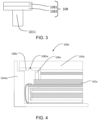
FIG. 3 is a schematic structural diagram of an ink layer and a barrier block according to the first embodiment of the present invention. -
FIG. 4 is a schematic structural diagram of a display device according to a second embodiment of the present invention. -
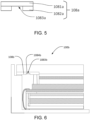
FIG. 5 is a schematic structural diagram of an ink layer and a slot according to the second embodiment of the present invention. -
FIG. 6 is a schematic structural diagram of a display device according to a third embodiment of the present invention. -
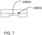
FIG. 7 is a schematic structural diagram of an ink layer, a slot, and a printing ink layer according to the third embodiment of the present invention. - Reference numerals of the present invention are:
-
display device 100; -
middle frame 104;first substrate 101;second substrate 102; -
cover plate 103;ink layer 108;silicone glue 109; -
bottom plate 1041;side frame 1042;barrier block 1011; -
lower polarizer 105;upper polarizer 106; optically clear adhesive (OCA)glue layer 107; -
backlight structure 110;backplate 111;reflective layer 112; -
light guide plate 113;scattering layer 114;prism layer 115; -
backlight source 117; chip onfilm 1012;support plate 1111; -
side plate 1112;spacer pad 116;display region 120; and - non-display
region 130. - The specific structure and functional details disclosed herein are only representative, and are used for the purpose of describing exemplary embodiments of the present application. However, the present application can be implemented in many alternative forms, and should not be interpreted as being limited only to the embodiments set forth herein.
- In the description of the present invention, it is to be understood that the terms such as "center", "transverse", "upper", "lower", "left", "right", "vertical", "horizontal", "top", "bottom", "inside", "outside", etc., the orientation or positional relationship of the indications is based on the orientation or positional relationship shown in the drawings, and is merely for the convenience of the description of the application and the simplified description, rather than indicating or implying that the device or component referred to has a specific orientation, in a specific orientation. The construction and operation are therefore not to be construed as limiting the invention. In addition, the terms "first" and "second" are only used for descriptive purposes, and cannot be understood as indicating or implying relative importance or implicitly indicating the number of indicated technical features. Thus, the features defined with "first" and "second" may explicitly or implicitly include one or more of these features. In the description of this application, unless otherwise specified, "plurality" means two or more. In addition, the term "including" and any variations thereof is intended to cover non-exclusive inclusion.
- In the description of the present application, it should be noted that the terms "installation", "connected", and "coupled" should be understood in a broad sense, unless explicitly stated and limited otherwise. For example, they may be fixed connections, removable connected or integrally connected; it can be mechanical, electrical, or can communicate with each other; it can be directly connected, or it can be indirectly connected through an intermediate medium, it can be an internal communication of two elements or an interaction relationship of two elements. For those of ordinary skill in the art, the specific meanings of the above terms in the present application can be understood according to specific situations.
- The terms used herein are only for describing specific embodiments and are not intended to limit the exemplary embodiments. Unless the context clearly dictates otherwise, the singular forms "a" and "one" used herein are also intended to include the plural. It should also be understood that the terms "including" and/or "including" used herein specify the existence of the stated features, integers, steps, operations, units and/or components, and do not exclude the existence or addition of one or more other features, integers, steps, operations, units, components, and/or combinations thereof.
- As shown in
FIG. 2 , a first embodiment of the present invention provides adisplay device 100, which includes amiddle frame 104, afirst substrate 101, asecond substrate 102, acover plate 103, anink layer 108, and asilicone glue 109. - The
middle frame 104 includes abottom plate 1041 and aside frame 1042, theside frame 1042 is disposed perpendicular to thebottom plate 1041, and themiddle frame 104 is formed integrally. Of course, in other embodiments, themiddle frame 104 can also adopt a split structure and be formed by assembly and combination. - The
first substrate 101 includes adisplay region 120 and anon-display region 130, and thefirst substrate 101 is positioned above thebottom plate 1041. Thefirst substrate 101 is an array substrate. - The
second substrate 102 is positioned above thedisplay region 120 of thefirst substrate 101, and thesecond substrate 102 is a color filter substrate. - In the present embodiment, a liquid crystal layer is provided between the
first substrate 101 and thesecond substrate 102. Because the present invention does not involve a structure of the liquid crystal layer, it is not shown inFIG. 2 . - The
cover plate 103 is disposed above thesecond substrate 102 and theside frame 1042. - The
ink layer 108 is disposed on a side of thecover plate 103 close to thefirst substrate 101 and corresponds to thenon-display region 130. A part of theink layer 108 is positioned corresponding to a position of themiddle frame 104, specifically, is disposed in an L-shaped opening of themiddle frame 104, and is bonded to themiddle frame 104 through an adhesive layer. - The
silicone glue 109 is disposed between theink layer 108 and thefirst substrate 101 and corresponds to thenon-display region 130. - A
barrier structure 1011 is provided on a side of theink layer 108 close to thefirst substrate 101. - The
barrier structure 1011 is a barrier block, and thebarrier structure 1011 is disposed between thesilicone glue 109 and theside frame 1042. - The
barrier structure 1011 is configured to block precipitation and diffusion of thesilicone glue 109, and a material of the barrier block includes ink. A thickness of the barrier block is same as a thickness of thesilicone glue 109. - The ink used as the barrier block has a special formula and printing process, and has a function of preventing the diffusion of pollution sources (silicone oil). The ink requires a smooth surface and is not prone to physical diffusion such as capillary.
- As shown in
FIG. 3 , theink layer 108 includes afirst ink layer 1081 and acover bottom layer 1082. - The
first ink layer 1081 is disposed on the side of thecover plate 103 close to thefirst substrate 101. - The
cover bottom layer 1082 is disposed on a side of thefirst ink layer 1081 away from thecover plate 103. - The
barrier structure 1011 is disposed on a side of thecover bottom layer 1082 away from thefirst ink layer 1081. - The barrier block is formed by printing a barrier ink, times of printing is not less than one printing, and a printing thickness is greater than 7um. In a printing process of a glass cover plate 103 (such as black ink), after a main body black and a ground black (i.e. the ink layer 108) are printed, a step of "barrier ink" is added to form the
barrier block 1011, and a region of that is finally cleaned. - A surface pattern of the barrier block can be made into a stripe shape or a grid shape, or a shape with a flat surface, to prevent capillary phenomenon on a surface of the
ink layer 108. - In an embodiment, the
display device 100 further includes alower polarizer 105, anupper polarizer 106, an optically clear adhesive (OCA)glue layer 107, and abacklight structure 110. - The
lower polarizer 105 is disposed on a side of thefirst substrate 101 away from thesecond substrate 102. - The
upper polarizer 106 is disposed on a side of thesecond substrate 102 away from thefirst substrate 101. - The
OCA glue layer 107 is disposed between theupper polarizer 106 and thecover plate 103. - The
backlight structure 110 is disposed between thelower polarizer 105 and thebottom plate 1041. - The
backlight structure 110 includes abackplate 111, areflective layer 112, alight guide plate 113, ascattering layer 114, aprism layer 115, and abacklight source 117. - The
backplate 111 includes asupport plate 1111 and aside plate 1112, and theside plate 1112 is disposed perpendicular to thesupport plate 1111. - The
reflective layer 112 is disposed on thesupport plate 1111. Thelight guide plate 113 is disposed on thereflective layer 112. Thescattering layer 114 is disposed on thelight guide plate 113. Theprism layer 115 is disposed on thescattering layer 114. Thebacklight source 117 is disposed at one end of thelight guide plate 113 and is disposed on theside plate 1112. - A
spacer pad 116 is provided between theside plate 1112 and thelower polarizer 105, a chip-on-film 1012 is provided on thelower polarizer 105, and the chip-on-film 1012 is bent downward to a bottom of thesupport plate 1111. - The first embodiment of the present invention provides a
display device 100, and by providing thebarrier structure 1011 disposed on the side of theink layer 108 close to thefirst substrate 101, thebarrier structure 1011 is disposed between thesilicone glue 109 and theside frame 1042 to prevent theink layer 108 on thecover plate 103 from spreading of a pollution source, so that the surface of theink layer 108 of theglass cover plate 103 of a display module can meet dyne specification requirements. It also ensures an adhesive strength of themiddle frame 104 and thecover plate 103 to prevent bonding failure. - As shown in
FIG. 4 andFIG. 5 , a second embodiment of the present invention provides thedisplay device 100a. Compared with the first embodiment, the difference lies in that theink layer 108a is provided with abarrier structure 1083a on a side close to thefirst substrate 101a. Thebarrier structure 1083a is a slot. - The slot extends from an upper surface of the cover bottom layer 1082a downward to an upper surface of the
first ink layer 1081a. - The slot is defined between the
side frame 1042 and thesilicone glue 109, and the slot is a blocking slot for separating a diffusion channel of thesilicone glue 109. - In the second embodiment, during an ink printing process of the
first ink layer 1081a and the cover bottom layer 1082a, before finishing a printing process of the final cover bottom layer 1082a, theslot 1083a is patterned by a printing screen, and finally cleaned. - The second embodiment of the present invention provides the
display device 100a, and by providing the slot (barrier structure 1083a) disposed on the side of theink layer 108 close to thefirst substrate 101, the slot is defined between thesilicone glue 109a and theside frame 1042a to prevent theink layer 108a from spreading of a pollution source, so that the surface of theink layer 108 of theglass cover plate 103 of the display module can meet dyne specification requirements. It also ensures an adhesive strength of the middle frame 104a and thecover plate 103a to prevent bonding failure. - As shown in
FIG. 6 andFIG. 7 , a third embodiment of the present invention provides thedisplay device 100b. Compared with the second embodiment, the difference lies in that aprinting ink layer 1084b is provided inside the slot (barrier structure 1083b) of theink layer 108b. - The
printing ink layer 1084b can prevent the physical diffusion of pollution sources, and a barrier effect of the third embodiment is better than that of the second embodiment. - Embodiments of the present invention have been described, but not intended to impose any unduly constraint to the appended claims. For a person skilled in the art, any modification of equivalent structure or equivalent process made according to the disclosure and drawings of the present invention, or any application thereof, directly or indirectly, to other related fields of technique, is considered encompassed in the scope of protection defined by the claims of the present invention.
Claims (13)
- A display device, comprising:a middle frame comprising a bottom plate and a side frame;a first substrate comprising a display region and a non-display region disposed above the bottom plate;a second substrate disposed above the display region of the first substrate;a cover plate disposed above the second substrate and the side frame;an ink layer disposed on a side of the cover plate close to the first substrate and corresponding to the non-display region, wherein a part of the ink layer is positioned corresponding to the middle frame; anda silicone glue disposed between the ink layer and the first substrate and corresponding to the non-display region;wherein a barrier structure is provided on a side of the ink layer close to the first substrate.
- The display device according to claim 1, wherein the barrier structure comprises a slot.
- The display device according to claim 1, wherein the barrier structure comprises a barrier block.
- The display device according to claim 1, wherein the ink layer comprises a first ink layer disposed on the side of the cover plate close to the first substrate, and a cover bottom layer disposed on a side of the first ink layer away from the cover plate.
- The display device according to claim 3, wherein the barrier block is disposed between the side frame and the silicone glue.
- The display device according to claim 5, wherein a thickness of the barrier block is same as a thickness of the silicone glue.
- The display device according to claim 3, wherein a material of the barrier block comprises ink.
- The display device according to claim 5, wherein the barrier block is disposed on a side of the cover bottom layer away from the first ink layer.
- The display device according to claim 2, wherein the slot is defined between the side frame and the silicone glue.
- The display device according to claim 9, wherein the slot extends downward to an upper surface of the first ink layer.
- The display device according to claim 9, wherein a printing ink layer is arranged in the slot.
- The display device according to claim 1, further comprising:a lower polarizer disposed on a side of the first substrate away from the second substrate;an upper polarizer disposed on a side of the second substrate away from the first substrate;an optically clear adhesive (OCA) glue layer disposed between the upper polarizer and the cover plate; anda backlight structure disposed between the lower polarizer and the bottom plate.
- The display device according to claim 9, wherein the backlight structure comprises:a backplate comprising a support plate and a side plate;a reflective layer disposed on the support plate;a light guide plate disposed on the reflective layer;a scattering layer disposed on the light guide plate;a prism layer disposed on the scattering layer; anda backlight source disposed at an end of the light guide plate and disposed on the side plate.
Priority Applications (1)
| Application Number | Priority Date | Filing Date | Title |
|---|---|---|---|
| EP25224894.3A EP4707881A3 (en) | 2020-08-05 | 2020-08-24 | Display device |
Applications Claiming Priority (2)
| Application Number | Priority Date | Filing Date | Title |
|---|---|---|---|
| CN202010775853.8A CN111965871B (en) | 2020-08-05 | 2020-08-05 | Display device |
| PCT/CN2020/110775 WO2022027737A1 (en) | 2020-08-05 | 2020-08-24 | Display device |
Related Child Applications (2)
| Application Number | Title | Priority Date | Filing Date |
|---|---|---|---|
| EP25224894.3A Division EP4707881A3 (en) | 2020-08-05 | 2020-08-24 | Display device |
| EP25224894.3A Division-Into EP4707881A3 (en) | 2020-08-05 | 2020-08-24 | Display device |
Publications (3)
| Publication Number | Publication Date |
|---|---|
| EP4198620A1 true EP4198620A1 (en) | 2023-06-21 |
| EP4198620A4 EP4198620A4 (en) | 2024-08-28 |
| EP4198620B1 EP4198620B1 (en) | 2026-01-28 |
Family
ID=77179128
Family Applications (2)
| Application Number | Title | Priority Date | Filing Date |
|---|---|---|---|
| EP25224894.3A Pending EP4707881A3 (en) | 2020-08-05 | 2020-08-24 | Display device |
| EP20880380.9A Active EP4198620B1 (en) | 2020-08-05 | 2020-08-24 | Display device |
Family Applications Before (1)
| Application Number | Title | Priority Date | Filing Date |
|---|---|---|---|
| EP25224894.3A Pending EP4707881A3 (en) | 2020-08-05 | 2020-08-24 | Display device |
Country Status (2)
| Country | Link |
|---|---|
| US (1) | US11086157B1 (en) |
| EP (2) | EP4707881A3 (en) |
Families Citing this family (6)
| Publication number | Priority date | Publication date | Assignee | Title |
|---|---|---|---|---|
| CN110045541B (en) * | 2019-03-28 | 2021-02-26 | 武汉华星光电技术有限公司 | Backlight structure, liquid crystal display panel and electronic equipment |
| CN114023916A (en) * | 2021-10-20 | 2022-02-08 | 业成科技(成都)有限公司 | Curved cover plate preparation method, curved cover plate and electronic equipment |
| KR20230126241A (en) * | 2022-02-21 | 2023-08-30 | 삼성디스플레이 주식회사 | display device |
| CN114527606B (en) | 2022-03-02 | 2024-04-05 | 武汉华星光电技术有限公司 | Display module and display device |
| TWI864543B (en) * | 2022-12-30 | 2024-12-01 | 晨豐光電股份有限公司 | Glass display cover with patterned structure and manufacturing method thereof |
| CN118736966B (en) * | 2024-06-27 | 2025-11-14 | 昆山国显光电有限公司 | Cover plate, display device, and method for manufacturing the cover plate |
Family Cites Families (9)
| Publication number | Priority date | Publication date | Assignee | Title |
|---|---|---|---|---|
| JPH0627442A (en) | 1992-07-09 | 1994-02-04 | Nec Kagoshima Ltd | Color liquid crystal display device |
| JP5938858B2 (en) * | 2011-07-27 | 2016-06-22 | 三菱電機株式会社 | Display device |
| US20150168767A1 (en) | 2012-06-11 | 2015-06-18 | Sharp Kabushiki Kaisha | Display device |
| JP6291397B2 (en) * | 2014-10-28 | 2018-03-14 | 株式会社ジャパンディスプレイ | Liquid crystal display |
| CN105607332A (en) | 2016-01-04 | 2016-05-25 | 京东方科技集团股份有限公司 | Color film substrate, display panel and display device |
| CN107942570A (en) | 2017-11-01 | 2018-04-20 | 广东欧珀移动通信有限公司 | A terminal, a display component, and a color filter substrate |
| CN110376780B (en) | 2019-07-20 | 2024-04-02 | 深圳阜时科技有限公司 | Under-screen detection system, liquid crystal display device and backlight module |
| CN110853522B (en) | 2019-11-29 | 2023-06-20 | 武汉天马微电子有限公司 | Display screen device |
| CN111128024B (en) * | 2019-12-30 | 2021-10-29 | 厦门天马微电子有限公司 | Display device |
-
2020
- 2020-08-24 US US17/049,355 patent/US11086157B1/en active Active
- 2020-08-24 EP EP25224894.3A patent/EP4707881A3/en active Pending
- 2020-08-24 EP EP20880380.9A patent/EP4198620B1/en active Active
Also Published As
| Publication number | Publication date |
|---|---|
| EP4707881A3 (en) | 2026-05-13 |
| EP4198620B1 (en) | 2026-01-28 |
| EP4707881A2 (en) | 2026-03-11 |
| EP4198620A4 (en) | 2024-08-28 |
| US11086157B1 (en) | 2021-08-10 |
Similar Documents
| Publication | Publication Date | Title |
|---|---|---|
| US11086157B1 (en) | Display device | |
| CN111965871B (en) | Display device | |
| EP0789295B1 (en) | Display unit having a transparent touchswitch and a liquid crystal display, and manufacturing method of the same | |
| KR100718560B1 (en) | Liquid Crystal Display and Manufacturing Method Thereof | |
| CN111736402B (en) | Display plasma module and display device | |
| US20120107980A1 (en) | Liquid crystal display device and method of fabricating the same | |
| KR101797244B1 (en) | In-plane switching mode liquid crystal display | |
| WO2007119409A1 (en) | Large-sized substrate and liquid crystal device employing the large-sized substrate and method for producing the liquid crystal device | |
| CN115527439A (en) | Display module, terminal and manufacturing method of display module | |
| US20080239208A1 (en) | Polymer Dispersed Liquid Crystal Formulations for Modulator Fabrication | |
| CN210199447U (en) | Vehicle-mounted display screen device and automobile | |
| US20050077005A1 (en) | Method for fabricating electro-optic light modulator | |
| TW201502679A (en) | Electrophoretic device, manufacturing method for electrophoretic device, and electronic apparatus | |
| JP2006235010A (en) | Electro-optic display device and manufacturing method thereof | |
| CN109212850A (en) | Liquid crystal display panel preparation method and liquid crystal display panel | |
| TW569065B (en) | Liquid crystal display panel | |
| US12498605B2 (en) | Display module and display apparatus | |
| JPH1083247A (en) | Display device | |
| EA044047B1 (en) | DISPLAY DEVICE | |
| CN109633962B (en) | display device | |
| CN101866080A (en) | LCD panel | |
| CN212276176U (en) | Display panel and terminal | |
| CN219302836U (en) | Dye liquid crystal color-changing film | |
| JP2005234309A (en) | Optical component manufacturing method, optical component | |
| US20140104540A1 (en) | Liquid crystal panel and the apparatus using the same |
Legal Events
| Date | Code | Title | Description |
|---|---|---|---|
| STAA | Information on the status of an ep patent application or granted ep patent |
Free format text: STATUS: UNKNOWN |
|
| STAA | Information on the status of an ep patent application or granted ep patent |
Free format text: STATUS: THE INTERNATIONAL PUBLICATION HAS BEEN MADE |
|
| PUAI | Public reference made under article 153(3) epc to a published international application that has entered the european phase |
Free format text: ORIGINAL CODE: 0009012 |
|
| STAA | Information on the status of an ep patent application or granted ep patent |
Free format text: STATUS: REQUEST FOR EXAMINATION WAS MADE |
|
| 17P | Request for examination filed |
Effective date: 20210507 |
|
| AK | Designated contracting states |
Kind code of ref document: A1 Designated state(s): AL AT BE BG CH CY CZ DE DK EE ES FI FR GB GR HR HU IE IS IT LI LT LU LV MC MK MT NL NO PL PT RO RS SE SI SK SM TR |
|
| DAV | Request for validation of the european patent (deleted) | ||
| DAX | Request for extension of the european patent (deleted) | ||
| A4 | Supplementary search report drawn up and despatched |
Effective date: 20240730 |
|
| RIC1 | Information provided on ipc code assigned before grant |
Ipc: G02B 6/00 20060101ALI20240724BHEP Ipc: G02F 1/13357 20060101ALI20240724BHEP Ipc: G02F 1/1335 20060101ALI20240724BHEP Ipc: G02F 1/1333 20060101AFI20240724BHEP |
|
| GRAP | Despatch of communication of intention to grant a patent |
Free format text: ORIGINAL CODE: EPIDOSNIGR1 |
|
| STAA | Information on the status of an ep patent application or granted ep patent |
Free format text: STATUS: GRANT OF PATENT IS INTENDED |
|
| INTG | Intention to grant announced |
Effective date: 20250819 |
|
| GRAS | Grant fee paid |
Free format text: ORIGINAL CODE: EPIDOSNIGR3 |
|
| GRAA | (expected) grant |
Free format text: ORIGINAL CODE: 0009210 |
|
| STAA | Information on the status of an ep patent application or granted ep patent |
Free format text: STATUS: THE PATENT HAS BEEN GRANTED |
|
| AK | Designated contracting states |
Kind code of ref document: B1 Designated state(s): AL AT BE BG CH CY CZ DE DK EE ES FI FR GB GR HR HU IE IS IT LI LT LU LV MC MK MT NL NO PL PT RO RS SE SI SK SM TR |
|
| P01 | Opt-out of the competence of the unified patent court (upc) registered |
Free format text: CASE NUMBER: UPC_APP_0018308_4198620/2025 Effective date: 20251218 |
|
| REG | Reference to a national code |
Ref country code: CH Ref legal event code: F10 Free format text: ST27 STATUS EVENT CODE: U-0-0-F10-F00 (AS PROVIDED BY THE NATIONAL OFFICE) Effective date: 20260128 Ref country code: GB Ref legal event code: FG4D |
|
| REG | Reference to a national code |
Ref country code: DE Ref legal event code: R096 Ref document number: 602020066284 Country of ref document: DE |
|
| REG | Reference to a national code |
Ref country code: IE Ref legal event code: FG4D |