EP4198527A1 - Method and system for determining a capacitance value - Google Patents
Method and system for determining a capacitance value Download PDFInfo
- Publication number
- EP4198527A1 EP4198527A1 EP22214049.3A EP22214049A EP4198527A1 EP 4198527 A1 EP4198527 A1 EP 4198527A1 EP 22214049 A EP22214049 A EP 22214049A EP 4198527 A1 EP4198527 A1 EP 4198527A1
- Authority
- EP
- European Patent Office
- Prior art keywords
- transformed
- capacitor
- current signal
- voltage signal
- determining
- Prior art date
- Legal status (The legal status is an assumption and is not a legal conclusion. Google has not performed a legal analysis and makes no representation as to the accuracy of the status listed.)
- Pending
Links
Images




Classifications
-
- G—PHYSICS
- G01—MEASURING; TESTING
- G01R—MEASURING ELECTRIC VARIABLES; MEASURING MAGNETIC VARIABLES
- G01R27/00—Arrangements for measuring resistance, reactance, impedance, or electric characteristics derived therefrom
- G01R27/02—Measuring real or complex resistance, reactance, impedance, or other two-pole characteristics derived therefrom, e.g. time constant
- G01R27/26—Measuring inductance or capacitance; Measuring quality factor, e.g. by using the resonance method; Measuring loss factor; Measuring dielectric constants ; Measuring impedance or related variables
- G01R27/2605—Measuring capacitance
-
- G—PHYSICS
- G01—MEASURING; TESTING
- G01R—MEASURING ELECTRIC VARIABLES; MEASURING MAGNETIC VARIABLES
- G01R19/00—Arrangements for measuring currents or voltages or for indicating presence or sign thereof
- G01R19/02—Measuring effective values, i.e. root-mean-square values
-
- G—PHYSICS
- G01—MEASURING; TESTING
- G01R—MEASURING ELECTRIC VARIABLES; MEASURING MAGNETIC VARIABLES
- G01R27/00—Arrangements for measuring resistance, reactance, impedance, or electric characteristics derived therefrom
- G01R27/02—Measuring real or complex resistance, reactance, impedance, or other two-pole characteristics derived therefrom, e.g. time constant
- G01R27/08—Measuring resistance by measuring both voltage and current
Definitions
- the present disclosure relates generally to capacitors. More specifically, the present disclosure relates to determining a capacitance value of a capacitor.
- Capacitors are commonly used components in electrical devices or systems. For example, capacitors are used as filters in power packs, inverters, etc. Factors like temperature fluctuations, voltage fluctuations, humidity fluctuations, increased vibrations and ripple currents, and variations in a load can lead to fluctuations in capacitance of a capacitor. The fluctuations in the capacitance can lead to failure or an un-interrupted downtime of the electrical device. Hence, continuous monitoring and detection of fault is needed to detect degradation in the capacitor. Inductance (L), Capacitance (C), and Resistance (R) (LCR) meter is a commonly known device to estimate the capacitance value of a capacitance. The LCR meter is used as an off-line technique and can be an intrusive measurement technique.
- One aspect of the present disclosure provides a method for determining a capacitance value of a capacitor.
- the method includes receiving a current signal flowing through the capacitor and receiving a voltage signal applied across the capacitor.
- the received voltage signal and the received current signal are filtered with a low pass filter.
- the filtered voltage signal and the filtered current signal are then discretized.
- the discretized voltage signal and the discretized current signal are transformed into a frequency domain.
- the capacitance value of the capacitor is determined from the transformed voltage signal and the transformed current signal.
- Another aspect of the present disclosure provides a method for determining a capacitance value of a capacitor.
- the method includes receiving a current signal flowing through the capacitor and receiving a voltage signal applied across the capacitor.
- the received voltage signal and the received current signal are filtered with a low pass filter.
- the filtered voltage signal and the filtered current signal are sampled.
- a fast Fourier transform is performed for each of the sampled voltage signal and the sampled current signal.
- An impedance of the capacitor is determined from the transformed voltage signal and the transformed current signal.
- a capacitive reactance of the capacitor is determined from an imaginary part of the impedance.
- the capacitance value of the capacitor is determined from the capacitive reactance.
- Yet another aspect of the present disclosure provides a method for determining a capacitance value of a capacitor.
- the method includes receiving a current signal flowing through the capacitor and receiving a voltage signal applied across the capacitor.
- the received voltage signal and the received current signal are filtered with a low pass filter.
- the filtered voltage signal and the filtered current signal are discretized.
- a fast Fourier transform is performed for each of the sampled voltage signal and the sampled current signal. Magnitudes of the transformed current signal and the transformed voltage signal are filtered at a pre-defined frequency with a band pass filter.
- An impedance of the capacitor is determined from the filtered magnitudes of the transformed current signal and the transformed voltage signal.
- the capacitance value of the capacitor is determined from the determined impedance.
- the present disclosure provides techniques for determining a capacitance value of a capacitor.
- the capacitance value is estimated passively during the operation of the capacitor.
- the capacitance value is estimated from a current signal flowing through the capacitor and a voltage signal applied across the capacitor at a dominant frequency and at a ripple frequency.
- FIG. 1 illustrates an example operating environment 100 in accordance with examples of the present disclosure.
- example environment 100 includes a capacitor 102, a current sensor 104, a voltage sensor 106, and a capacitance estimator 108.
- environment 100 further includes an input side and an output side.
- the input side may include a power source and the output side may include an electrical load, for example, a motor.
- Capacitor 102 can be part of an electrical device, for example, an invertor driving the motor.
- capacitor 102 can be a ceramic capacitor, a film and paper capacitor, a polymer capacitor, an electrolytic capacitor, etc.
- Current sensor 104 measures a current flowing though capacitor 102.
- current sensor 104 measures the current flowing through capacitor 102 using a magnetic field and without interrupting the working of capacitor 102.
- Voltage sensor 106 measures a voltage applied across the capacitor. Voltage sensor 106 also measures the voltage applied across capacitor 102 without interrupting the working of capacitor 102.
- the current flowing through capacitor 102 and measured by current sensor 104 is represented in time domain as current signal I(t).
- the voltage applied across capacitor 102 and measured by voltage sensor 106 can be represented in time domain as voltage signal V(t).
- the current signal I(t) and the voltage signal V(t) are time domain analog signals.
- Capacitance estimator 108 determines or estimates the capacitance value of capacitor 102 from the current signal I(t) and the voltage signal V(t) received from current sensor 104 and voltage sensor 106 respectively.
- capacitance estimator 108 estimates the capacitance value of capacitor 102 passively without interrupting the functioning of capacitor 102. That is, capacitance estimator 108 can estimate the capacitance value of capacitor 102 during use, that is, when capacitor 102 is online. Thus, capacitance estimator 108 can estimate the capacitance value of capacitor 102 without taking capacitor 102 offline.
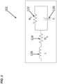
- Figure 2 illustrates an equivalent model of capacitor 102.
- discrete capacitors such as capacitor 102
- Capacitor 102 deviate from ideal capacitors that only stores and releases electrical energy with no dissipation.
- Capacitor 102 unlike ideal capacitor has losses and parasitic inductive parts.
- properties of capacitor 102 can be defined and specified by the equivalent circuit or model shown in Figure 2 .
- the equivalent model of capacitor 102 is composed of an idealized capacitor (C) 120, a parallel resistor (Rp) 122, a series resistor (Rs) 124, and an inductor (L) 126.
- Parallel resistor (Rp) 122 may represent an insulation resistance (Rins) of a dielectric material of capacitor 102 and a resistance representing a leakage current (Rleak) of capacitor 102.
- Series resistor (Rs) 124 may represent ohmic losses of capacitor 102 and is also referred to as an Equivalent Series Resistor (ESR).
- Inductor (L) 126 may represent a self-inductance of capacitor 102 and is also referred to as an Equivalent Series Inductance (ESL).
- both, idealized capacitance (C) 120 and inductor (L) 126 are frequency driven impedances and thus can vary with the frequency.
- inductor (L) 126 may be small and its influence can generally be seen only at high frequencies.
- FIG 3 illustrates an impedance spectrum 130 of capacitor 102.
- impedance spectrum 130 of capacitor 102 is generally V-shaped.
- the capacitive characteristics that is, the capacitive impedance X C
- the reactive impedance X L cancel each other out, and the total impedance is purely resistive parts, that is, series resistor (Rs) 124 or ESR, of capacitor 102.
- the inductive characteristics that is, the inductive impedance X L
- the inductive impedance X L the inductive impedance of capacitor 102 is dominant.
- the self-resonating frequency is a frequency at which the capacitive impedance X C and the reactive impedance X L of capacitor 102 cause equally large but opposite impedances.
- the impedance characteristics at different frequencies can be used to determine the capacitance value of capacitor 102.
- FIG. 4 illustrates components of capacitance estimator 108 in accordance with principles of the present disclosure.
- capacitor estimator 108 includes a low pass filter 142, an analog to digital convertor 144, a window operator 146, a Fast Fourier Transform (FFT) operator 148, a first estimator 150, a band pass filter 152, a Root Mean Square (RMS) calculator 154, and a second estimator 156.
- FFT Fast Fourier Transform
- first estimator 150 a band pass filter 152
- RMS Root Mean Square
- second estimator 108 may include additional or less components than those depicted. The functioning of the components of capacitor estimator 108 will be described in the following sections of the disclosure in combination with methods of determining the capacitance value of capacitor 102.
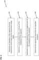
- Figure 5 illustrates a flow diagram of a method 200 for determining the capacitance value of capacitor 102.
- method 200 can be performed by capacitance estimator 108.
- method 200 is performed by a processor connected to a memory device.
- the memory device may store the instructions which, when executed by the processor, perform method 200.
- the current signal I(t) and the voltage signal V(t) are received or acquired.
- the current signal I(t) is received from current sensor 104 and the voltage signal V(t) is received from voltage sensor 106.
- the current signal I(t) and the voltage signal V(t) are received at low pass filter 142.
- low pass filter 142 can be connected to each of current sensor 104 and voltage sensor 106 and receives the current signal I(t) from current sensor 104 and the voltage signal V(t) from voltage sensor 106.
- the received current signal I(t) and the received voltage signal V(t) are filtered.
- the received current signal I(t) and the voltage signal V(t) are filtered using low pass filter 142.
- the current signal I(t) and the voltage signal V(t) are filtered simultaneously or in parallel.
- low pass filter 142 can include multiple filters for filtering the current signal I(t) and the voltage signal V(t) simultaneously.
- the current signal I(t) and the voltage signal V(t) can be filtered simultaneously using dedicated low pass filters 142.
- Low pass filter 142 allows signals with a frequency lower than a selected cut-off frequency and attenuates signals with frequencies higher than the cut-off frequency.
- the cut-off frequency can be selected as a dominant frequency, a ripple frequency, or a switching frequency.
- the cut-off frequency can be a multiple of a dominant frequency, a ripple frequency, and/or a switching frequency.
- the cut-off frequency can be harmonics of a dominant frequency, a ripple frequency, and /or a switching frequency.
- the dominant frequency is the frequency with a maximum amplitude.
- the switching frequency is the frequency at which the inverter is operating.
- the dominant frequency and the switching frequency can depend on the inverter design and applications.
- the switching frequency can be either 8kHz or 12 kHz.
- the ripple frequency is the higher order frequency components of either the dominant frequency or the switching frequency.
- the ripple frequency can be dominant as compared to its fundamental frequency.
- the filtered current signal I(t) and the filtered voltage signal V(t) are discretized.
- the filtered current signal I(t) and the filtered voltage signal V(t) are discretized by sampling.
- the current signal I(t) and the voltage signal V(t) are sampled using Analog to Digital Convertor (ADC) 144.
- ADC 144 is connected to low pass filter 142 and receives the filtered current signal I(t) and the filtered voltage signal V(t) from low pass filter 142.
- a rate of sampling can be pre-defined.
- the current signal I(t) and the voltage signal V(t) may be sampled at a rate of 32 samples per cycle.
- the filtered current signal I(t) and the filtered voltage signal V(t) can be reduced from continuous time signals to discrete time signals.
- sampling is performed by measuring a value of the current signal I(t) and the voltage signal V(t) over a sampling interval or a sampling period represented by T seconds.
- the filtered current signal I(t) and the filtered voltage signal V(t) can be sampled simultaneously or in parallel. For example, each of the filtered current signal I(t) and the filtered voltage signal V(t) can be sampled simultaneously using dedicated ADCs 144.
- the rate of sampling can be lower compared to that at the switching frequency.
- the sampling rate or the sampling frequency can be 5 to 10 times of the frequency of interest.
- the frequency of interest can be either one of the dominant frequency, the switching frequency, or the ripple frequency.
- the sampling period is the inverse of the sampling frequency.
- windowing is performed on the discretized current signal I(t) and the discretized voltage signal V(t).
- the windowing is performed by window operator 146.
- window operator 146 can be connected to ADC 144 and receives the discretized current signal I(t) and the discretized voltage signal V(t) from ADC 144. Window operator 146 then performs the windowing on the discretized current signal I(t) and the discretized voltage signal V(t). During windowing, the discretized current signal I(t) and voltage signal V(t) are multiplied by a pre-defined window function.
- the product of the multiplication has a zero value outside a chosen interval and all that is remaining is where the discretized current signal I(t) and voltage signal V(t) and the window function overlap.
- the window function is a finite length window with an amplitude that varies smoothly and gradually toward zero at the edges.
- the window function can include a Hanning window function.
- the windowing is performed on the discretized current signal I(t) and the discretized voltage signal V(t) to detect transient events and time averaging of frequency spectra.
- the discretized current signal I(t) and the discretized voltage signal V(t) are windowed simultaneously or in parallel. For example, each of the discretized current signal I(t) and the discretized voltage signal V(t) can be filtered simultaneously using dedicated window operators 146.
- the windowed discretized current signal I(t) and the windowed discretized voltage signal V(t) are transformed into a frequency domain.
- the windowed discretized current signal I(t) and the windowed discretized voltage signal V(t) are transformed into the frequency domain using Fast Fourier Transform (FFT) operator 148.
- FFT operator 148 can be connected to window operator 146 and receives the windowed discretized current signal I(t) and the windowed discretized voltage signal V(t) from window operator 146.
- FFT operator 148 then transforms the windowed discretized current signal I(t) and the windowed discretized voltage signal V(t) from the time domain to frequency domain.
- FFT operator 148 determines discrete Fourier transform of each of the windowed discretized current signal I(t) and the windowed discretized voltage signal V(t).
- the frequency domain representation of the windowed discretized current signal I(t) and the windowed discretized voltage signal V(t) shows currents and voltages present at different frequencies.
- the windowed discretized current signal I(t) and the windowed discretized voltage signal V(t) are transformed simultaneously or in parallel. For example, each of the windowed discretized current signal I(t) and the windowed discretized voltage signal V(t) are transformed simultaneously using dedicated FFT operators 148.
- the capacitance value of capacitor 102 is determined from the transformed current signal I(t) and the transformed voltage signal V(t).
- the disclosure provides two methods to determine the capacitance value of capacitor 102 from the transformed current signal I(t) and the transformed voltage signal V(t).
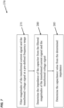
- Figure 6 illustrates first method 240 for determining the capacitance value of capacitor 102 from the transformed current signal I(t) and the transformed voltage signal V(t).
- first method 240 is performed by capacitance estimator 108.
- method 240 is performed by a processor connected to a memory device. The memory device may store the instructions which, when executed by the processor, perform method 240.
- an impedance Z of capacitor 102 is determined from the transformed current I(t) and voltage V(t) signals.
- the impedance Z of capacitor 102 is determined by first estimator 150.
- first estimator 150 is connected to FFT operator 148 and receives the transformed current signal I(t) and the transformed voltage signal V(t) from FFT operator 150.
- First estimator 150 determines the impedance Z from the transformed current signal I(t) and the transformed voltage signal V(t).
- the impedance Z is determined by dividing the transformed voltage signal V(t) with the transformed current signal I(t). For example, the transformed voltage signal V(t) is divided by the transformed current signal I(t) at a dominant frequency, where the amplitudes of the current signal I(t) and voltage signal V(t) are maximum.
- a resultant vector diagram of impedance Z is shown in Figure 8 .
- the vector diagram of the impedance Z is also referred to as an impedance triangle where the sides of the triangle represent the real and imaginary portions of the impedance Z.
- the discretized current signal I(t) and the discretized voltage signal V(t) can be transformed at the dominant frequencies ( f df ), the ripple frequency ( f rf ), or at their respective harmonics using FFT operator 148.
- V ( kf rf ) and I ( kf rf ) are the voltage and current values obtained from the FFT carried out on the windowed discretized current signal I[n] and the windowed discretized voltage signal V[n] at the ripple frequency and where k is ⁇ 1, 2, 3,4, 5, ... ⁇ .
- V ( kf df ) and I ( kf df ) are the voltage and current values obtained from the FFT carried out on the windowed discretized current signal I[n] and the windowed discretized voltage signal V[n] at the dominating frequency and where k is ⁇ 1, 2, 3, 4, 5, ... ⁇ .
- a capacitive reactance is estimated from an imaginary part of the impedance Z.
- X C ZSin ( ⁇ ) ( or ) imag ( Z ).
- the capacitive reactance X C is determined by first estimator 150.
- the capacitance value of capacitor 102 is determined from the capacitive reactance X C .
- the capacitance values that is, C estm 1 ( kfr f ) and C estm 1 ( kf df ) from the capacitive reactance X C are determined by first estimator 150.
- Figure 7 illustrates a second method 270 for determining the capacitance value of capacitor 102.
- Second method 270 utilizes the dominant frequency to determine the capacitance value.
- method 270 can be performed by capacitance estimator 108.
- method 270 is performed by a processor connected to a memory device. The memory device may store the instructions which, when executed by the processor, perform method 270.
- the windowed discretized time series signals (that is, the windowed discretized voltage signal V y [ n ] and the windowed discretized current signal I y [ n ]) are obtained by passing the discretized current signal I[n] and the discretized voltage signal V[n] through a window function w [ n ] to obtain the windowed discretized current signal I y [ n ] and the windowed discretized voltage signal V y [ n ] respectively.
- the windowed discretized voltage signal V y ( n ) and the windowed discretized current signal I y ( n ) are converted into the frequency domain using FFT operator 148.
- Second method 270 determines the capacitance value of capacitor 102 from the magnitudes of the voltage signal V [ k ] and the current signal I [ k ] in the frequency domain.
- the magnitudes of the voltage signal V [ k ] and the current signal I [ k ] are filtered at a pre-defined frequency range.
- the magnitudes of the voltage signal V [ k ] and the current signal I [ k ] are filtered at the pre-defined range using band pass filter 152.
- band pass filter 152 is connected to FFT operator 148 and receives the magnitudes of the voltage signal V [ k ] and the current signal I [ k ] from FFT operator 148.
- Band pass filter 152 then filters both the magnitude of the voltage signal V [ k ] and the magnitude of the current signal I [ k ] at the pre-defined range.
- band pass filter 152 can include multiple filters for filtering the magnitudes of the current signal I [ k ] and the voltage signal V [ k ] simultaneously.
- the magnitudes of each of the current signal I [ k ] and the voltage signal V [ k ] are filtered simultaneously using dedicated band pass filters 152.
- pre-defined range of the bandpass filtered is centered around either one of the dominant frequency, the ripple frequency, or the switching frequency with a variable deviation. The deviation or bandwidth can be far smaller than the dominant frequency, the ripple frequency, or the switching frequency.
- pre-defined range is determined as a center frequency plus upper cutoff frequency and the center frequency minus lower cutoff frequency, where the center frequency is one of the dominant frequency, the ripple frequency, or the switching frequency.
- band pass filter 152 passes frequencies within the pre-defined range and attenuates frequencies outside of that range.
- the pre-defined range is centered around the dominating frequency, the ripple frequency, or their harmonics.
- the impedance Z is determined from the filtered magnitudes of the current signal I kf df [ k ] and the voltage signal V kf df [ k ] .
- the impedance Z is calculated from Root Mean Square (RMS) values of the filtered current signal I kf df [ k ] and the voltage signal V kf df [ k ].
- RMS calculator 154 is connected to band pass filter 152 and receives the filtered magnitudes of the current signal I kf df [ k ] and the voltage signal V kf df [ k ] from band pass filter 152.
- RMS calculator 152 determines the RMS values of the filtered magnitudes of the current signal I kf df [ k ] and the voltage signal V kf df [ k ] .
- the RMS values of the filtered magnitudes of the current signal I kf df [ k ] and the voltage signal V kf df [ k ] are determined simultaneously or in parallel.
- the RMS values for each of the filtered magnitudes of the current signal I kf df [ k ] and the voltage signal V kf df [ k ] are determined simultaneously using dedicated RMS calculators 152.
- the Z estm 2 is determined by second estimator 156.
- second estimator 156 is connected to RMS calculator 154 and receives the RMS values of each of the filtered magnitudes of the current signal I kf df [ k ] and the voltage signal V kf df [ k ] from RMS calculator 154.
- Second estimator 156 determines Z estm 2 from the RMS values of the filtered magnitudes of the current signal I kf df [ k ] and the voltage signal V kf df [ k ] .
- the capacitance value of capacitor 102 is determined from the impedance value Z estm 2 .
- the C estm 2 is determined by second estimator 156.
- the techniques disclosed herein provide a real time online estimate of the capacitance value and ESR 124 of capacitor 102.
- the disclosed techniques use the dominant and/or ripple frequencies for analysis, therefore, estimation of the parameters can be achieved at low sampling rate (for example, 10kHz). Due to a lower sampling rate, the techniques disclosed herein can be implemented on an embedded board with lower memory.
- the techniques disclosed herein are independent of type, manufacturer, and make of capacitor 102.
- the techniques disclosed herein are applicable for individual capacitor as well as capacitor banks.
- the estimation errors are independent of the load and or Revolution Per Minute (RPM) of the load under test.
- RPM Revolution Per Minute
- the techniques disclosed herein can be used for online estimation of the capacitance value and ESR 124 of Direct Current (DC) capacitor in High Voltage DC (HVDC) fuel pump application.
- the techniques disclosed herein can be applied to individual, as well as, bank level capacitors used in a DC link various other applications like inverters, converters, etc.
- it can be used in Uninterrupted Power Supply (UPS) applications, HVDC fuel pumps, Alternate Fuel Transfer Manifolds (AFTMs), industrial drives, aircrafts, and electric vehicles-inverters/converters, etc.
- UPS Uninterrupted Power Supply
- HVDC fuel pumps Alternate Fuel Transfer Manifolds (AFTMs)
- AFTMs Alternate Fuel Transfer Manifolds
- industrial drives aircrafts
- aircrafts and electric vehicles-inverters/converters, etc.
- a method for determining a capacitance value of a capacitor comprising:
- Aspect 2 The method of Aspect 1, wherein filtering each of the received voltage signal and the received current signal with the low pass filter comprises filtering each of the received voltage signal and the received current signal with the low pass filter at one of the following: a dominant frequency and a ripple frequency.
- a method for determining a capacitance value of a capacitor comprising:
- Aspect 7 The method of Aspect 6, wherein determining the impedance of the capacitor from the filtered magnitudes of the transformed current signal and the transformed voltage signal comprises:
- Aspect 9 The method of Aspect 6, wherein filtering the magnitudes of the transformed current signal and the transformed voltage signal at the pre-defined frequency comprises filtering the magnitudes of the transformed current signal and the transformed voltage signal at a dominant frequency with a band pass filter.
- Aspect 10 The method of Aspect 6, further comprising windowing the discretized voltage signal and the discretized current signal.
Landscapes
- Physics & Mathematics (AREA)
- General Physics & Mathematics (AREA)
- Measurement Of Resistance Or Impedance (AREA)
Abstract
A method for determining a capacitance value of a capacitor is provided. The method includes receiving a current signal flowing through the capacitor and receiving a voltage signal applied across the capacitor. The received voltage signal and the received current signal are filtered with a low pass filter. The filtered voltage signal and the filtered current signal are then discretized. The discretized voltage signal and the discretized current signal are transformed into a frequency domain. The capacitance value of the capacitor is determined from the transformed voltage signal and the transformed current signal.
Description
- The present disclosure relates generally to capacitors. More specifically, the present disclosure relates to determining a capacitance value of a capacitor.
- Capacitors are commonly used components in electrical devices or systems. For example, capacitors are used as filters in power packs, inverters, etc. Factors like temperature fluctuations, voltage fluctuations, humidity fluctuations, increased vibrations and ripple currents, and variations in a load can lead to fluctuations in capacitance of a capacitor. The fluctuations in the capacitance can lead to failure or an un-interrupted downtime of the electrical device. Hence, continuous monitoring and detection of fault is needed to detect degradation in the capacitor. Inductance (L), Capacitance (C), and Resistance (R) (LCR) meter is a commonly known device to estimate the capacitance value of a capacitance. The LCR meter is used as an off-line technique and can be an intrusive measurement technique.
- One aspect of the present disclosure provides a method for determining a capacitance value of a capacitor. The method includes receiving a current signal flowing through the capacitor and receiving a voltage signal applied across the capacitor. The received voltage signal and the received current signal are filtered with a low pass filter. The filtered voltage signal and the filtered current signal are then discretized. The discretized voltage signal and the discretized current signal are transformed into a frequency domain. The capacitance value of the capacitor is determined from the transformed voltage signal and the transformed current signal.
- Another aspect of the present disclosure provides a method for determining a capacitance value of a capacitor. The method includes receiving a current signal flowing through the capacitor and receiving a voltage signal applied across the capacitor. The received voltage signal and the received current signal are filtered with a low pass filter. The filtered voltage signal and the filtered current signal are sampled. A fast Fourier transform is performed for each of the sampled voltage signal and the sampled current signal. An impedance of the capacitor is determined from the transformed voltage signal and the transformed current signal. A capacitive reactance of the capacitor is determined from an imaginary part of the impedance. The capacitance value of the capacitor is determined from the capacitive reactance.
- Yet another aspect of the present disclosure provides a method for determining a capacitance value of a capacitor. The method includes receiving a current signal flowing through the capacitor and receiving a voltage signal applied across the capacitor. The received voltage signal and the received current signal are filtered with a low pass filter. The filtered voltage signal and the filtered current signal are discretized. A fast Fourier transform is performed for each of the sampled voltage signal and the sampled current signal. Magnitudes of the transformed current signal and the transformed voltage signal are filtered at a pre-defined frequency with a band pass filter. An impedance of the capacitor is determined from the filtered magnitudes of the transformed current signal and the transformed voltage signal. The capacitance value of the capacitor is determined from the determined impedance.
- These and other features and advantages will be apparent from a reading of the following detailed description and a review of the associated drawings. A variety of additional aspects will be set forth in the description that follows. These aspects can relate to individual features and to combinations of features. It is to be understood that both the foregoing general description and the following detailed description are exemplary and explanatory only and are not restrictive of the broad concepts upon which the embodiments disclosed herein are based.
- The accompanying drawings which are incorporated in and constitute a part of the description, illustrate several aspects of the disclosure. A brief description of the drawings is as follows:
-
Figure 1 illustrates an example environment in accordance with principles of the present disclosure. -
Figure 2 illustrates an equivalent model of a capacitor. -
Figure 3 illustrates an impedance spectrum of a capacitor. -
Figure 4 illustrates components of a capacitance estimator. -
Figure 5 illustrates a flow diagram of a method for determining the capacitance value of a capacitor. -
Figure 6 illustrate a flow diagram of a first method for determining the capacitance value of a capacitor. -
Figure 7 illustrates a flow diagram of a second method for determining the capacitance value of a capacitor. -
Figure 8 illustrates an impedance triangle of a capacitor. - Reference will now be made in detail to exemplary aspects of the present disclosure that are illustrated in the accompanying drawings. Wherever possible, the same reference numbers will be used throughout the drawings to refer to the same or like structure.
- The present disclosure provides techniques for determining a capacitance value of a capacitor. The capacitance value is estimated passively during the operation of the capacitor. In certain examples, the capacitance value is estimated from a current signal flowing through the capacitor and a voltage signal applied across the capacitor at a dominant frequency and at a ripple frequency.
-
Figure 1 illustrates anexample operating environment 100 in accordance with examples of the present disclosure. As illustrated inFigure 1 ,example environment 100 includes acapacitor 102, acurrent sensor 104, avoltage sensor 106, and acapacitance estimator 108. In certain examples,environment 100 further includes an input side and an output side. The input side may include a power source and the output side may include an electrical load, for example, a motor. Capacitor 102 can be part of an electrical device, for example, an invertor driving the motor. In certain examples,capacitor 102 can be a ceramic capacitor, a film and paper capacitor, a polymer capacitor, an electrolytic capacitor, etc. -
Current sensor 104 measures a current flowing thoughcapacitor 102. In some examples,current sensor 104 measures the current flowing throughcapacitor 102 using a magnetic field and without interrupting the working ofcapacitor 102.Voltage sensor 106 measures a voltage applied across the capacitor.Voltage sensor 106 also measures the voltage applied acrosscapacitor 102 without interrupting the working ofcapacitor 102. In examples, the current flowing throughcapacitor 102 and measured bycurrent sensor 104 is represented in time domain as current signal I(t). Similarly, the voltage applied acrosscapacitor 102 and measured byvoltage sensor 106 can be represented in time domain as voltage signal V(t). In certain examples, the current signal I(t) and the voltage signal V(t) are time domain analog signals. -
Current sensor 104 andvoltage sensor 106 provide the measured current signal I(t) and the measured voltage signal V(t) tocapacitance estimator 108. For example,capacitance estimator 108 can be connected to bothcurrent sensor 104 andvoltage sensor 106.Capacitance estimator 108 determines or estimates the capacitance value ofcapacitor 102 from the current signal I(t) and the voltage signal V(t) received fromcurrent sensor 104 andvoltage sensor 106 respectively. In certain examples and discussed in greater detail in the following portions of the specification,capacitance estimator 108 estimates the capacitance value ofcapacitor 102 passively without interrupting the functioning ofcapacitor 102. That is,capacitance estimator 108 can estimate the capacitance value ofcapacitor 102 during use, that is, whencapacitor 102 is online. Thus,capacitance estimator 108 can estimate the capacitance value ofcapacitor 102 without takingcapacitor 102 offline. -
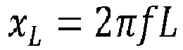
Figure 2 illustrates an equivalent model ofcapacitor 102. In examples, discrete capacitors, such ascapacitor 102, deviate from ideal capacitors that only stores and releases electrical energy with no dissipation.Capacitor 102, unlike ideal capacitor has losses and parasitic inductive parts. Hence, properties ofcapacitor 102 can be defined and specified by the equivalent circuit or model shown inFigure 2 . As shown inFigure 2 , the equivalent model ofcapacitor 102 is composed of an idealized capacitor (C) 120, a parallel resistor (Rp) 122, a series resistor (Rs) 124, and an inductor (L) 126. Parallel resistor (Rp) 122 may represent an insulation resistance (Rins) of a dielectric material ofcapacitor 102 and a resistance representing a leakage current (Rleak) ofcapacitor 102. Series resistor (Rs) 124 may represent ohmic losses ofcapacitor 102 and is also referred to as an Equivalent Series Resistor (ESR). Inductor (L) 126 may represent a self-inductance ofcapacitor 102 and is also referred to as an Equivalent Series Inductance (ESL). - In certain examples, both, idealized capacitance (C) 120 and inductor (L) 126 are frequency driven impedances and thus can vary with the frequency. For example, capacitive impendence XC is calculated as:

-
Figure 3 illustrates animpedance spectrum 130 ofcapacitor 102. As shown inFigure 3 ,impedance spectrum 130 ofcapacitor 102 is generally V-shaped. For example, up until a self-resonating frequency, the capacitive characteristics (that is, the capacitive impedance XC) ofcapacitor 102 is dominant. At the self-resonating frequency, the capacitive impedance XC and the reactive impedance XL cancel each other out, and the total impedance is purely resistive parts, that is, series resistor (Rs) 124 or ESR, ofcapacitor 102. After the self-resonating frequency, the inductive characteristics (that is, the inductive impedance XL) ofcapacitor 102 is dominant. In examples, the self-resonating frequency is a frequency at which the capacitive impedance XC and the reactive impedance XL ofcapacitor 102 cause equally large but opposite impedances. In other examples, the impedance characteristics at different frequencies can be used to determine the capacitance value ofcapacitor 102. -
Figure 4 illustrates components ofcapacitance estimator 108 in accordance with principles of the present disclosure. As shown,capacitor estimator 108 includes alow pass filter 142, an analog todigital convertor 144, awindow operator 146, a Fast Fourier Transform (FFT)operator 148, afirst estimator 150, aband pass filter 152, a Root Mean Square (RMS)calculator 154, and asecond estimator 156. In other examples,capacitance estimator 108 may include additional or less components than those depicted. The functioning of the components ofcapacitor estimator 108 will be described in the following sections of the disclosure in combination with methods of determining the capacitance value ofcapacitor 102. -
Figure 5 illustrates a flow diagram of amethod 200 for determining the capacitance value ofcapacitor 102. In certain examples,method 200 can be performed bycapacitance estimator 108. In other examples,method 200 is performed by a processor connected to a memory device. The memory device may store the instructions which, when executed by the processor, performmethod 200. - At
block 205 ofmethod 200, the current signal I(t) and the voltage signal V(t) are received or acquired. For example, the current signal I(t) is received fromcurrent sensor 104 and the voltage signal V(t) is received fromvoltage sensor 106. In certain examples, the current signal I(t) and the voltage signal V(t) are received atlow pass filter 142. For example,low pass filter 142 can be connected to each ofcurrent sensor 104 andvoltage sensor 106 and receives the current signal I(t) fromcurrent sensor 104 and the voltage signal V(t) fromvoltage sensor 106. - At
block 210 ofmethod 200, the received current signal I(t) and the received voltage signal V(t) are filtered. The received current signal I(t) and the voltage signal V(t) are filtered usinglow pass filter 142. In certain examples, the current signal I(t) and the voltage signal V(t) are filtered simultaneously or in parallel. For examples,low pass filter 142 can include multiple filters for filtering the current signal I(t) and the voltage signal V(t) simultaneously. The current signal I(t) and the voltage signal V(t) can be filtered simultaneously using dedicated low pass filters 142. -
Low pass filter 142, in some examples, allows signals with a frequency lower than a selected cut-off frequency and attenuates signals with frequencies higher than the cut-off frequency. In certain examples, the cut-off frequency can be selected as a dominant frequency, a ripple frequency, or a switching frequency. In other examples, the cut-off frequency can be a multiple of a dominant frequency, a ripple frequency, and/or a switching frequency. In some other examples, the cut-off frequency can be harmonics of a dominant frequency, a ripple frequency, and /or a switching frequency. The dominant frequency is the frequency with a maximum amplitude. The switching frequency is the frequency at which the inverter is operating. The dominant frequency and the switching frequency can depend on the inverter design and applications. In some examples, the switching frequency can be either 8kHz or 12 kHz. The ripple frequency is the higher order frequency components of either the dominant frequency or the switching frequency. In some examples, the ripple frequency can be dominant as compared to its fundamental frequency. - At
block 215 ofmethod 200, the filtered current signal I(t) and the filtered voltage signal V(t) are discretized. In certain examples, the filtered current signal I(t) and the filtered voltage signal V(t) are discretized by sampling. The current signal I(t) and the voltage signal V(t) are sampled using Analog to Digital Convertor (ADC) 144. For example,ADC 144 is connected tolow pass filter 142 and receives the filtered current signal I(t) and the filtered voltage signal V(t) fromlow pass filter 142. - A rate of sampling can be pre-defined. For example, the current signal I(t) and the voltage signal V(t) may be sampled at a rate of 32 samples per cycle. During sampling, the filtered current signal I(t) and the filtered voltage signal V(t) can be reduced from continuous time signals to discrete time signals. In certain examples, sampling is performed by measuring a value of the current signal I(t) and the voltage signal V(t) over a sampling interval or a sampling period represented by T seconds. The filtered current signal I(t) and the filtered voltage signal V(t) can be sampled simultaneously or in parallel. For example, each of the filtered current signal I(t) and the filtered voltage signal V(t) can be sampled simultaneously using
dedicated ADCs 144. In certain examples, since the filtered current signal I(t) and the filtered voltage signal V(t) are at the dominant frequency and the ripple frequency, the rate of sampling can be lower compared to that at the switching frequency. In examples, the sampling rate or the sampling frequency can be 5 to 10 times of the frequency of interest. The frequency of interest can be either one of the dominant frequency, the switching frequency, or the ripple frequency. The sampling period is the inverse of the sampling frequency. - At
block 220 ofmethod 200, windowing is performed on the discretized current signal I(t) and the discretized voltage signal V(t). In examples, the windowing is performed bywindow operator 146. For example,window operator 146 can be connected toADC 144 and receives the discretized current signal I(t) and the discretized voltage signal V(t) fromADC 144.Window operator 146 then performs the windowing on the discretized current signal I(t) and the discretized voltage signal V(t). During windowing, the discretized current signal I(t) and voltage signal V(t) are multiplied by a pre-defined window function. The product of the multiplication has a zero value outside a chosen interval and all that is remaining is where the discretized current signal I(t) and voltage signal V(t) and the window function overlap. In certain examples, the window function is a finite length window with an amplitude that varies smoothly and gradually toward zero at the edges. In certain examples, the window function can include a Hanning window function. In certain examples, the windowing is performed on the discretized current signal I(t) and the discretized voltage signal V(t) to detect transient events and time averaging of frequency spectra. In examples, the discretized current signal I(t) and the discretized voltage signal V(t) are windowed simultaneously or in parallel. For example, each of the discretized current signal I(t) and the discretized voltage signal V(t) can be filtered simultaneously usingdedicated window operators 146. - At
block 225 ofmethod 200, the windowed discretized current signal I(t) and the windowed discretized voltage signal V(t) are transformed into a frequency domain. In certain examples, the windowed discretized current signal I(t) and the windowed discretized voltage signal V(t) are transformed into the frequency domain using Fast Fourier Transform (FFT)operator 148. For example,FFT operator 148 can be connected towindow operator 146 and receives the windowed discretized current signal I(t) and the windowed discretized voltage signal V(t) fromwindow operator 146.FFT operator 148 then transforms the windowed discretized current signal I(t) and the windowed discretized voltage signal V(t) from the time domain to frequency domain. For example,FFT operator 148 determines discrete Fourier transform of each of the windowed discretized current signal I(t) and the windowed discretized voltage signal V(t). - In certain examples, the frequency domain representation of the windowed discretized current signal I(t) and the windowed discretized voltage signal V(t) shows currents and voltages present at different frequencies. In certain examples, the windowed discretized current signal I(t) and the windowed discretized voltage signal V(t) are transformed simultaneously or in parallel. For example, each of the windowed discretized current signal I(t) and the windowed discretized voltage signal V(t) are transformed simultaneously using
dedicated FFT operators 148. - At
block 230 ofmethod 200, the capacitance value ofcapacitor 102 is determined from the transformed current signal I(t) and the transformed voltage signal V(t). In some examples and discussed in greater detail in the following portions, the disclosure provides two methods to determine the capacitance value ofcapacitor 102 from the transformed current signal I(t) and the transformed voltage signal V(t). -
Figure 6 illustratesfirst method 240 for determining the capacitance value ofcapacitor 102 from the transformed current signal I(t) and the transformed voltage signal V(t). In some examples,first method 240 is performed bycapacitance estimator 108. In other examples,method 240 is performed by a processor connected to a memory device. The memory device may store the instructions which, when executed by the processor, performmethod 240. - At
block 245 offirst method 240, an impedance Z ofcapacitor 102 is determined from the transformed current I(t) and voltage V(t) signals. In certain examples, the impedance Z ofcapacitor 102 is determined byfirst estimator 150. For example,first estimator 150 is connected toFFT operator 148 and receives the transformed current signal I(t) and the transformed voltage signal V(t) fromFFT operator 150.First estimator 150 then determines the impedance Z from the transformed current signal I(t) and the transformed voltage signal V(t). - In certain examples, the impedance Z is determined by dividing the transformed voltage signal V(t) with the transformed current signal I(t). For example, the transformed voltage signal V(t) is divided by the transformed current signal I(t) at a dominant frequency, where the amplitudes of the current signal I(t) and voltage signal V(t) are maximum. For example, the impedance Z is represented as:


Figure 8 . The vector diagram of the impedance Z is also referred to as an impedance triangle where the sides of the triangle represent the real and imaginary portions of the impedance Z. - In certain examples, the discretized current signal I(t) and the discretized voltage signal V(t) can be transformed at the dominant frequencies (fdf ), the ripple frequency (frf ), or at their respective harmonics using
FFT operator 148. Hence, the impedance Z at the ripple frequency is calculated as:

- At
block 250 offirst method 240,ESR 124 forcapacitor 102 is determined from a real part of the impedance Z. For example, from the impedance triangle ofFigure 8 , ESR = ZCos(θ) (or) real(Z). Hence,ESR 124 at the ripple frequency is calculated as:
ESR 124 at the dominating frequency is calculated as:
ESR 124 is determined byfirst estimator 150. - At
block 255 offirst method 240, a capacitive reactance is estimated from an imaginary part of the impedance Z. For example, from the impedance triangle ofFigure 8 , XC = ZSin(θ) (or) imag(Z). Hence, the capacitive reactance XC at the ripple frequency is calculated as:

first estimator 150. - At
block 260 offirst method 240, the capacitance value ofcapacitor 102 is determined from the capacitive reactance XC. For example, the capacitance value ofcapacitor 102 at the ripple frequency is calculated from the capacitive reactance XC as:
ESR 124 and the estimated capacitance value ofcapacitor 102 at the ripple frequency. Similarly, the capacitance value ofcapacitor 102 at the dominant frequency is calculated from the capacitive reactance XC as:
ESR 124 and the estimated capacitance value ofcapacitor 102 at the dominating frequency. In certain examples, the capacitance values (that is, C estm1(kfrf ) and C estm1(kfdf )) from the capacitive reactance XC are determined byfirst estimator 150. -
Figure 7 illustrates asecond method 270 for determining the capacitance value ofcapacitor 102.Second method 270 utilizes the dominant frequency to determine the capacitance value. In certain examples,method 270 can be performed bycapacitance estimator 108. In other examples,method 270 is performed by a processor connected to a memory device. The memory device may store the instructions which, when executed by the processor, performmethod 270. - In certain examples, the windowed discretized time series signals (that is, the windowed discretized voltage signal Vy [n] and the windowed discretized current signal Iy [n]) are obtained by passing the discretized current signal I[n] and the discretized voltage signal V[n] through a window function w[n] to obtain the windowed discretized current signal Iy [n] and the windowed discretized voltage signal Vy [n] respectively. For example, the windowed discretized voltage signal Vy [n] is calculated as:


- In certain examples, the windowed discretized voltage signal Vy (n) and the windowed discretized current signal I y(n) are converted into the frequency domain using
FFT operator 148. For example, the windowed discretized voltage signal Vy (n) is converted into the frequency domain as:

Second method 270 determines the capacitance value ofcapacitor 102 from the magnitudes of the voltage signal V[k] and the current signal I[k] in the frequency domain. - For example, at
block 275 ofsecond method 270, the magnitudes of the voltage signal V[k] and the current signal I[k] are filtered at a pre-defined frequency range. In certain examples, the magnitudes of the voltage signal V[k] and the current signal I[k] are filtered at the pre-defined range usingband pass filter 152. For example,band pass filter 152 is connected toFFT operator 148 and receives the magnitudes of the voltage signal V[k] and the current signal I[k] fromFFT operator 148.Band pass filter 152 then filters both the magnitude of the voltage signal V[k] and the magnitude of the current signal I[k] at the pre-defined range. In certain examples, the magnitudes of the current signal I[k] and the voltage signal V[k] are filtered simultaneously or in parallel. For examples,band pass filter 152 can include multiple filters for filtering the magnitudes of the current signal I[k] and the voltage signal V[k] simultaneously. For example, the magnitudes of each of the current signal I[k] and the voltage signal V[k] are filtered simultaneously using dedicated band pass filters 152. In certain examples, pre-defined range of the bandpass filtered is centered around either one of the dominant frequency, the ripple frequency, or the switching frequency with a variable deviation. The deviation or bandwidth can be far smaller than the dominant frequency, the ripple frequency, or the switching frequency. In certain examples, pre-defined range is determined as a center frequency plus upper cutoff frequency and the center frequency minus lower cutoff frequency, where the center frequency is one of the dominant frequency, the ripple frequency, or the switching frequency. - In certain examples,
band pass filter 152 passes frequencies within the pre-defined range and attenuates frequencies outside of that range. In some examples, the pre-defined range is centered around the dominating frequency, the ripple frequency, or their harmonics. For example, the magnitude of the voltage signal V[k] can be filtered at the dominating frequency as:

- At
block 280 ofsecond method 270, the impedance Z is determined from the filtered magnitudes of the current signal Ikfdf [k] and the voltage signal Vkfdf [k]. In examples, the impedance Z is calculated from Root Mean Square (RMS) values of the filtered current signal Ikfdf [k] and the voltage signal Vkfdf [k]. For example,RMS calculator 154 is connected to bandpass filter 152 and receives the filtered magnitudes of the current signal Ikfdf [k] and the voltage signal Vkfdf [k] fromband pass filter 152.RMS calculator 152 then determines the RMS values of the filtered magnitudes of the current signal Ikfdf [k] and the voltage signal Vkfdf [k]. In certain examples, the RMS values of the filtered magnitudes of the current signal Ikfdf [k] and the voltage signal Vkfdf [k] are determined simultaneously or in parallel. For example, the RMS values for each of the filtered magnitudes of the current signal Ikfdf [k] and the voltage signal Vkfdf [k] are determined simultaneously usingdedicated RMS calculators 152. - In certain examples, the impedance Z is calculated as:

second estimator 156. For example,second estimator 156 is connected toRMS calculator 154 and receives the RMS values of each of the filtered magnitudes of the current signal Ikfdf [k] and the voltage signal Vkfdf [k] fromRMS calculator 154.Second estimator 156 then determines Z estm2 from the RMS values of the filtered magnitudes of the current signal Ikfdf [k] and the voltage signal Vkfdf [k]. - At
block 285 ofsecond method 270, the capacitance value ofcapacitor 102 is determined from the impedance value Z estm2. For example, the capacitance value ofcapacitor 102 is calculated as:
second estimator 156. - In certain examples, the techniques disclosed herein provide a real time online estimate of the capacitance value and
ESR 124 ofcapacitor 102. The disclosed techniques use the dominant and/or ripple frequencies for analysis, therefore, estimation of the parameters can be achieved at low sampling rate (for example, 10kHz). Due to a lower sampling rate, the techniques disclosed herein can be implemented on an embedded board with lower memory. The techniques disclosed herein are independent of type, manufacturer, and make ofcapacitor 102. In addition, the techniques disclosed herein are applicable for individual capacitor as well as capacitor banks. Moreover, the estimation errors are independent of the load and or Revolution Per Minute (RPM) of the load under test. - In certain examples, the techniques disclosed herein can be used for online estimation of the capacitance value and
ESR 124 of Direct Current (DC) capacitor in High Voltage DC (HVDC) fuel pump application. In addition, the techniques disclosed herein can be applied to individual, as well as, bank level capacitors used in a DC link various other applications like inverters, converters, etc. Moreover, it can be used in Uninterrupted Power Supply (UPS) applications, HVDC fuel pumps, Alternate Fuel Transfer Manifolds (AFTMs), industrial drives, aircrafts, and electric vehicles-inverters/converters, etc. - Aspect 1. A method for determining a capacitance value of a capacitor, the method comprising:
- receiving a current signal flowing through the capacitor;
- receiving a voltage signal applied across the capacitor;
- filtering each of the received voltage signal and the received current signal with a low pass filter;
- sampling each of the filtered voltage signal and the filtered current signal;
- performing a fast Fourier transform of each of the sampled voltage signal and the sampled current signal;
- determining an impedance of the capacitor from the transformed voltage signal and the transformed current signal;
- determining a capacitive reactance of the capacitor from an imaginary part of the impedance; and
- determining the capacitance value of the capacitor from the capacitive reactance.
- Aspect 2. The method of Aspect 1, wherein filtering each of the received voltage signal and the received current signal with the low pass filter comprises filtering each of the received voltage signal and the received current signal with the low pass filter at one of the following: a dominant frequency and a ripple frequency.
- Aspect 3. The method of Aspect 1, wherein determining the impedance of the capacitor from the transformed voltage signal and the transformed current signal comprises determining the impedance as

- Aspect 4. The method of Aspect 3, further comprising determining the capacitive reactance of the capacitor from the imaginary part of the impedance as: XC (kf
df ) = imag(Z(kfdf )). - Aspect 5. The method of Aspect 4, further comprising determining the capacitance value of the capacitor from the capacitive reactance as:

- Aspect 6. A method for determining a capacitance value of a capacitor, the method comprising:
- receiving a current signal flowing through the capacitor;
- receiving a voltage signal applied across the capacitor;
- filtering each of the received voltage signal and the received current signal with a low pass filter;
- discretizing each of the filtered voltage signal and the filtered current signal;
- performing a fast Fourier transform of each of the discretized voltage signal and the discretized current signal;
- filtering magnitudes of the transformed current signal and the transformed voltage signal at a pre-defined frequency with a band pass filter;
- determining an impedance of the capacitor from the filtered magnitudes of the transformed current signal and the transformed voltage signal; and
- determining the capacitance value of the capacitor from the determined impedance.
- Aspect 7. The method of Aspect 6, wherein determining the impedance of the capacitor from the filtered magnitudes of the transformed current signal and the transformed voltage signal comprises:
- determining a Root Mean Square (RMS) value of the filtered magnitude of the transformed current signal;
- determining a RMS value of the filtered magnitude of the transformed current signal; and
- determining the impedance of the capacitor by dividing the RMS value of the filtered magnitude of the transformed current signal with the RMS value of the filtered magnitude of the transformed current signal.
- Aspect 8. The method of Aspect 6, wherein determining the capacitance value of the capacitor from the determined impedance comprises the capacitance value of the capacitor as:

- Aspect 9. The method of Aspect 6, wherein filtering the magnitudes of the transformed current signal and the transformed voltage signal at the pre-defined frequency comprises filtering the magnitudes of the transformed current signal and the transformed voltage signal at a dominant frequency with a band pass filter.
- Aspect 10. The method of Aspect 6, further comprising windowing the discretized voltage signal and the discretized current signal.
- From the forgoing detailed description, it will be evident that modifications and variations can be made without departing from the spirit and scope of the disclosure.
Claims (15)
- A method for determining a capacitance value of a capacitor, the method comprising:receiving a current signal flowing through the capacitor;receiving a voltage signal applied across the capacitor;filtering each of the received voltage signal and the received current signal with a low pass filter;discretizing each of the filtered voltage signal and the filtered current signal;transforming each of the discretized voltage signal and the discretized current signal into frequency domain; anddetermining the capacitance value of the capacitor from the transformed voltage signal and the transformed current signal.
- The method of claim 1, wherein determining the capacitance value of the capacitor from the transformed voltage signal and the transformed current signal comprises:determining an impedance of the capacitor from the transformed voltage signal and the transformed current signal;determining a capacitive reactance of the capacitor from an imaginary part of the impedance; anddetermining the capacitance value of the capacitor from the capacitive reactance.
- The method of claim 2, further comprising:
determining a series resistance of the capacitor from a real part of the impedance. - The method of claim 2, wherein determining the impedance of the capacitor from the transformed voltage signal and the transformed current signal comprises determining the impedance of the capacitor from the transformed voltage signal and the transformed current signal transformed at a dominant frequency.
- The method of claim 2, wherein determining the impedance of the capacitor from the transformed voltage signal and the transformed current signal comprises determining the impedance of the capacitor from the transformed voltage signal and the transformed current signal transformed at a ripple frequency.
- The method of claim 1, wherein determining the capacitance value of the capacitor from the transformed voltage signal and the transformed current signal comprises:filtering magnitudes of the transformed current signal and the transformed voltage signal at a pre-defined frequency;determining the impedance of the capacitor from the filtered magnitudes of the transformed current signal and the transformed voltage signal; anddetermining the capacitance value of the capacitor from the determined impedance.
- The method of claim 6, wherein determining the impedance of the capacitor from the filtered magnitudes of the transformed current signal and the transformed voltage signal comprises:determining a Root Mean Square (RMS) value of the filtered magnitude of the transformed current signal;determining a RMS value of the filtered magnitude of the transformed current signal; anddetermine the impedance of the capacitor by dividing the RMS value of the filtered magnitude of the transformed current signal with the RMS value of the filtered magnitude of the transformed current signal.
- The method of claim 6, wherein determining the capacitance value of the capacitor from the determined impedance comprises the capacitance value of the capacitor as:

- The method of claim 6, wherein filtering the magnitudes of the transformed current signal and the transformed voltage signal at the pre-defined frequency comprises filtering the magnitudes of the transformed current signal and the transformed voltage signal at a dominant frequency with a band pass filter.
- The method of claim 6, wherein determining the impedance of the capacitor from the transformed voltage signal and the transformed current signal comprises determining the impedance as

- The method of claim 10, further comprising determining the capacitive reactance of the capacitor from the imaginary part of the impedance as: XC (kfdf ) = imag(Z(kfdf )).
- The method of claim 11, further comprising determining the capacitance value of the capacitor from the capacitive reactance as:

- The method of claim 1, wherein filtering the magnitudes of the transformed current signal and the transformed voltage signal at the pre-defined frequency comprises filtering the magnitudes of the transformed current signal and the transformed voltage signal at a dominant frequency with a band pass filter.
- The method of claim 1, wherein transforming each of the discretized voltage signal and the discretized current signal into the frequency domain comprises performing a fast Fourier transform of each of the discretized voltage signal and the discretized current signal.
- The method of claim 1, wherein filtering each of the received voltage signal and the received current signal with the low pass filter comprises filtering each of the received voltage signal and the received current signal with the low pass filter at one of the following: a dominant frequency and a ripple frequency.
Applications Claiming Priority (1)
| Application Number | Priority Date | Filing Date | Title |
|---|---|---|---|
| IN202111058965 | 2021-12-17 |
Publications (1)
| Publication Number | Publication Date |
|---|---|
| EP4198527A1 true EP4198527A1 (en) | 2023-06-21 |
Family
ID=84537828
Family Applications (1)
| Application Number | Title | Priority Date | Filing Date |
|---|---|---|---|
| EP22214049.3A Pending EP4198527A1 (en) | 2021-12-17 | 2022-12-16 | Method and system for determining a capacitance value |
Country Status (2)
| Country | Link |
|---|---|
| US (1) | US20230194587A1 (en) |
| EP (1) | EP4198527A1 (en) |
Families Citing this family (2)
| Publication number | Priority date | Publication date | Assignee | Title |
|---|---|---|---|---|
| CN117871959A (en) * | 2023-12-29 | 2024-04-12 | 苏州长风航空电子有限公司 | Capacitance acquisition device of a capacitive sensor |
| CN119335442B (en) * | 2024-09-27 | 2025-10-28 | 南昌大学 | A method for monitoring the state of DC bus capacitor of photovoltaic inverter |
Citations (3)
| Publication number | Priority date | Publication date | Assignee | Title |
|---|---|---|---|---|
| GB2175700A (en) * | 1985-05-15 | 1986-12-03 | Secr Defence | Battery residual capacity measurement |
| CN107870265A (en) * | 2017-05-19 | 2018-04-03 | 中国矿业大学 | A detection method of grid-to-ground capacitance based on high-precision DFT |
| CN111220862A (en) * | 2019-10-31 | 2020-06-02 | 北京交通大学 | Method for monitoring residual life of direct current capacitor of three-phase uncontrolled rectification alternating current-direct current-alternating current system |
-
2022
- 2022-12-13 US US18/080,449 patent/US20230194587A1/en active Pending
- 2022-12-16 EP EP22214049.3A patent/EP4198527A1/en active Pending
Patent Citations (3)
| Publication number | Priority date | Publication date | Assignee | Title |
|---|---|---|---|---|
| GB2175700A (en) * | 1985-05-15 | 1986-12-03 | Secr Defence | Battery residual capacity measurement |
| CN107870265A (en) * | 2017-05-19 | 2018-04-03 | 中国矿业大学 | A detection method of grid-to-ground capacitance based on high-precision DFT |
| CN111220862A (en) * | 2019-10-31 | 2020-06-02 | 北京交通大学 | Method for monitoring residual life of direct current capacitor of three-phase uncontrolled rectification alternating current-direct current-alternating current system |
Non-Patent Citations (1)
| Title |
|---|
| SOLIMAN HAMMAM ET AL: "A Review of the Condition Monitoring of Capacitors in Power Electronic Converters", IEEE TRANSACTIONS ON INDUSTRY APPLICATIONS, IEEE SERVICE CENTER, PISCATAWAY, NJ, US, vol. 52, no. 6, 1 November 2016 (2016-11-01), pages 4976 - 4989, XP011634697, ISSN: 0093-9994, [retrieved on 20161118], DOI: 10.1109/TIA.2016.2591906 * |
Also Published As
| Publication number | Publication date |
|---|---|
| US20230194587A1 (en) | 2023-06-22 |
Similar Documents
| Publication | Publication Date | Title |
|---|---|---|
| US20230194587A1 (en) | Method and system for determining a capacitance value | |
| US10128650B2 (en) | Relay protection method and apparatus against LC parallel circuit detuning faults | |
| CN102401866B (en) | Detecting method of detuning fault element of triple-tuned DC filter | |
| EP3779475B1 (en) | Insulation detection circuit and insulation detection method | |
| CN104950180B (en) | Cell batteries internal resistance accurate measurement method based on EIS | |
| US10527666B2 (en) | Method and device for determining the fault location in the case of a fault on an electric line | |
| CN102998544A (en) | Method for diagnosing operating state of windings in short-circuiting of transformer | |
| Prasanth et al. | Online equivalent series resistance estimation method for condition monitoring of DC-link capacitors | |
| EP3971592A1 (en) | Fault location determination in a power transmission system | |
| US20130293258A1 (en) | Method and system for detecting a defect on the dc power supply bus of a power converter | |
| CN110161395B (en) | Method and system for monitoring insulation state of inverter driving motor on line | |
| CN115166515A (en) | Method for monitoring ground insulation of variable frequency motor on line based on leakage current frequency domain characteristics | |
| CN109375048A (en) | A transmission line parameter identification method and device based on fault recording data | |
| CN105301410A (en) | Method and device for online detection of electromagnetic compatibility performance of intelligent assembly of transformer substation | |
| CN112946515A (en) | Online monitoring method and device for converter transformer network side sleeve | |
| CN115792536A (en) | Method for online evaluation of main insulation state of variable frequency motor | |
| CN107017636A (en) | A kind of charging pile stress_responsive genes and filtering method | |
| CN1797014A (en) | Detection method for testing current in resistance property of lightning arrester | |
| US8600687B2 (en) | Signal analyzer for analyzing dynamic behavior of a target system | |
| Probst et al. | Using capacitive electric field sensors to measure transient overvoltages: A case study | |
| CN111505524A (en) | On-line monitoring method of cascade converter and applicable cascade converter | |
| CN113671410A (en) | Ground fault detection method and system for arc suppression coil and small resistance grounded distribution network | |
| CN113281668A (en) | Energy storage battery impedance identification method and system based on driving inverter and application | |
| CN120490872B (en) | Online Measurement Method of Internal Resistance of Multi-Frequency Small-Signal Discharge Based on Harmonic Analysis | |
| CN110346645A (en) | A kind of super capacitor internal resistance measuring method, device and computer readable storage medium |
Legal Events
| Date | Code | Title | Description |
|---|---|---|---|
| PUAI | Public reference made under article 153(3) epc to a published international application that has entered the european phase |
Free format text: ORIGINAL CODE: 0009012 |
|
| STAA | Information on the status of an ep patent application or granted ep patent |
Free format text: STATUS: REQUEST FOR EXAMINATION WAS MADE |
|
| 17P | Request for examination filed |
Effective date: 20221216 |
|
| AK | Designated contracting states |
Kind code of ref document: A1 Designated state(s): AL AT BE BG CH CY CZ DE DK EE ES FI FR GB GR HR HU IE IS IT LI LT LU LV MC ME MK MT NL NO PL PT RO RS SE SI SK SM TR |
|
| STAA | Information on the status of an ep patent application or granted ep patent |
Free format text: STATUS: EXAMINATION IS IN PROGRESS |
|
| 17Q | First examination report despatched |
Effective date: 20250605 |