EP4195902A1 - Elektrolumineszenzanzeige - Google Patents
Elektrolumineszenzanzeige Download PDFInfo
- Publication number
- EP4195902A1 EP4195902A1 EP22197692.1A EP22197692A EP4195902A1 EP 4195902 A1 EP4195902 A1 EP 4195902A1 EP 22197692 A EP22197692 A EP 22197692A EP 4195902 A1 EP4195902 A1 EP 4195902A1
- Authority
- EP
- European Patent Office
- Prior art keywords
- planarization layer
- pixel
- layer
- bank
- contact hole
- Prior art date
- Legal status (The legal status is an assumption and is not a legal conclusion. Google has not performed a legal analysis and makes no representation as to the accuracy of the status listed.)
- Pending
Links
Images




Classifications
-
- H—ELECTRICITY
- H10—SEMICONDUCTOR DEVICES; ELECTRIC SOLID-STATE DEVICES NOT OTHERWISE PROVIDED FOR
- H10K—ORGANIC ELECTRIC SOLID-STATE DEVICES
- H10K59/00—Integrated devices, or assemblies of multiple devices, comprising at least one organic light-emitting element covered by group H10K50/00
- H10K59/10—OLED displays
- H10K59/12—Active-matrix OLED [AMOLED] displays
- H10K59/131—Interconnections, e.g. wiring lines or terminals
- H10K59/1315—Interconnections, e.g. wiring lines or terminals comprising structures specially adapted for lowering the resistance
-
- H—ELECTRICITY
- H10—SEMICONDUCTOR DEVICES; ELECTRIC SOLID-STATE DEVICES NOT OTHERWISE PROVIDED FOR
- H10K—ORGANIC ELECTRIC SOLID-STATE DEVICES
- H10K59/00—Integrated devices, or assemblies of multiple devices, comprising at least one organic light-emitting element covered by group H10K50/00
- H10K59/10—OLED displays
- H10K59/12—Active-matrix OLED [AMOLED] displays
- H10K59/122—Pixel-defining structures or layers, e.g. banks
-
- H—ELECTRICITY
- H10—SEMICONDUCTOR DEVICES; ELECTRIC SOLID-STATE DEVICES NOT OTHERWISE PROVIDED FOR
- H10K—ORGANIC ELECTRIC SOLID-STATE DEVICES
- H10K59/00—Integrated devices, or assemblies of multiple devices, comprising at least one organic light-emitting element covered by group H10K50/00
- H10K59/10—OLED displays
- H10K59/12—Active-matrix OLED [AMOLED] displays
- H10K59/121—Active-matrix OLED [AMOLED] displays characterised by the geometry or disposition of pixel elements
-
- H—ELECTRICITY
- H10—SEMICONDUCTOR DEVICES; ELECTRIC SOLID-STATE DEVICES NOT OTHERWISE PROVIDED FOR
- H10K—ORGANIC ELECTRIC SOLID-STATE DEVICES
- H10K59/00—Integrated devices, or assemblies of multiple devices, comprising at least one organic light-emitting element covered by group H10K50/00
- H10K59/10—OLED displays
- H10K59/12—Active-matrix OLED [AMOLED] displays
- H10K59/121—Active-matrix OLED [AMOLED] displays characterised by the geometry or disposition of pixel elements
- H10K59/1213—Active-matrix OLED [AMOLED] displays characterised by the geometry or disposition of pixel elements the pixel elements being TFTs
-
- H—ELECTRICITY
- H10—SEMICONDUCTOR DEVICES; ELECTRIC SOLID-STATE DEVICES NOT OTHERWISE PROVIDED FOR
- H10K—ORGANIC ELECTRIC SOLID-STATE DEVICES
- H10K59/00—Integrated devices, or assemblies of multiple devices, comprising at least one organic light-emitting element covered by group H10K50/00
- H10K59/10—OLED displays
- H10K59/12—Active-matrix OLED [AMOLED] displays
- H10K59/123—Connection of the pixel electrodes to the thin film transistors [TFT]
-
- H—ELECTRICITY
- H10—SEMICONDUCTOR DEVICES; ELECTRIC SOLID-STATE DEVICES NOT OTHERWISE PROVIDED FOR
- H10K—ORGANIC ELECTRIC SOLID-STATE DEVICES
- H10K59/00—Integrated devices, or assemblies of multiple devices, comprising at least one organic light-emitting element covered by group H10K50/00
- H10K59/10—OLED displays
- H10K59/12—Active-matrix OLED [AMOLED] displays
- H10K59/124—Insulating layers formed between TFT elements and OLED elements
-
- H—ELECTRICITY
- H10—SEMICONDUCTOR DEVICES; ELECTRIC SOLID-STATE DEVICES NOT OTHERWISE PROVIDED FOR
- H10K—ORGANIC ELECTRIC SOLID-STATE DEVICES
- H10K59/00—Integrated devices, or assemblies of multiple devices, comprising at least one organic light-emitting element covered by group H10K50/00
- H10K59/10—OLED displays
- H10K59/12—Active-matrix OLED [AMOLED] displays
- H10K59/131—Interconnections, e.g. wiring lines or terminals
-
- H—ELECTRICITY
- H10—SEMICONDUCTOR DEVICES; ELECTRIC SOLID-STATE DEVICES NOT OTHERWISE PROVIDED FOR
- H10K—ORGANIC ELECTRIC SOLID-STATE DEVICES
- H10K59/00—Integrated devices, or assemblies of multiple devices, comprising at least one organic light-emitting element covered by group H10K50/00
- H10K59/80—Constructional details
- H10K59/805—Electrodes
- H10K59/8052—Cathodes
- H10K59/80522—Cathodes combined with auxiliary electrodes
Definitions
- the present disclosure relates to an electroluminescence display. Especially, the present disclosure relates to an electroluminescence display having an improved image quality stability by eliminating or blocking the lateral leakage current between neighboring pixels. In addition, the present disclosure relates to an electroluminescence display having an improved image quality stability by lowering the resistance of the cathod electrode adopting an auxiliary cathode line.
- CTRs cathode ray tubes
- LCDs liquid crystal displays
- PDPs plasma display panels
- electroluminescent displays are used to display image data of various products such as computer, mobile phones, bank deposit and withdrawal devices (ATMs), and vehicle navigation systems according to their unique characteristics and purposes.
- the organic light emitting diode display which is a self-luminous display, has excellent optical performance such as wide viewing angle and high color reproducibility, and its application field is gradually widened, so it is in the spotlight for an high quality image display device. Due to these advantages, it is attacting attention as the most suitable display device for implementing 8K ultra-high resolution displays beyond 4K. As the resolution is increased, the size of the emission area occupied in the pixel also becomes smaller. In order to maximize the size of the emission area, it is preferable to apply a top emission type structure.
- the transparent conductive material has a higher sheet resistance than the metal material, it may be difficult to maintain a constant cathode voltage when implementing a large-area display device. Accordingly, in a large area electroluminescent display having a top emission type, a structure for connecting to a signal line having a low-resistance may be required in order to lower the sheet resistance of the cathode electrode.
- the distance between pixels in the electroluminescence display becomes narrower.
- electrons or holes may leak in the lateral (or horizontal) direction along the functional layer included into the emission layer (or light emitting layer) between neighboring pixels.
- a problem of inaccurate color reproduction may be occurred.
- the purpose of the present disclosure is to provide an electroluminescence display having a large-area ultra-high resolution and excellent image quality.
- Another purpose of the present disclosure is to provide an electroluminescence display in which a cathode voltage may be maintained constant in a top emission type display suitable for implementing the ultra-high-resolution structure.
- Still another purpose of the present disclosure is to provide an ultra-high-resolution electroluminescence display that minimizes the effect of parasitic currents among densly arranged pixels.
- an electroluminescence display comprises: a pixel disposed on a substrate; a low resistance line disposed on one side of the pixel; a passivation layer on the low resistance line covering the entire substrate; a planarization layer on the passivation layer covering the entire substrate; a cathode contact hole exposing a part of the low resistance line; an anode electrode disposed on the planarization layer; an under-cut trench formed in the planarization layer disposed between the anode electrode and the cathode contact hole; a bank covering circumference area of the anode electrode; an emission layer on the bank, the anode electrode and the planarization layer and a cathode electrode on the emission layer, wherein the cathode electrode is connected to the low resistance line through the cathode contact hole.
- the electroluminescence display further comprises: a pixel trench formed by removing a part of the planarization layer as being around the anode electrode at outside of the bank.
- the pixel trench is formed by removing a part of the planarization layer adjacent to (or away from, or to a side of, or at an outside of) the anode electrode and/or the bank.
- the emission layer extends to a neighboring pixel through the pixel trench.
- the cathode contact hole is formed at some areas overlapped with the low resistance line at the pixel trench. In other words, the cathode contact hole overlaps the low resistance line in the pixel trench.
- the cathode contact hole includes: a first aperture formed at the passivation layer and having a first width; and a second aperture formed at the planarization layer and having a second width narrower than the first width.
- the emission layer is disposed on some of the low resistance line exposed as corresponding to the second width.
- the cathode electrode is connected to the low resistance line exposed as corresponding to the first width.
- a ratio of a depth of the under-cut trench to a thickness of the planarization layer is any one of 1:1 to 3:4.
- the bank is disposed between the anode electrode and the under-cut trench.
- the bank fills the under-cut trench and covers a part of the planarization layer.
- the bank does not cover portions of the planarization layer between the under-cut trench and the cathode contact hole.
- the electroluminescence display further comprises: a thin film transistor disposed under the passivation layer and connected to the anode electrode.
- the electroluminescence display comprises: a first pixel and a second pixel disposed next to each other on a substrate; a low resistance line disposed between the first pixel and the second pixel; a passivation layer on the low resistance line and covering the substrate; a first planarization layer disposed at the first pixel on the passivation layer; a second planarization layer disposed at the second pixel on the passivation layer; a first anode electrode on the first planarization layer; a second anode electrode on the second planarization layer; a cathode contact hole exposing a part of the low resistance line between the first planarization layer and the second planarization layer; a first under-cut trench formed at the first planarization layer between the first anode electrode and the cathode contact hole; a second under-cut trench formed at the second planarization layer between the second anode electrode and the cathode contact hole; a first bank covering circumference areas of the first anode electrode;
- the electroluminescence display further comprises: a pixel trench disposed between the first planarization layer and the second planarization layer, and exposing the passivation layer.
- the emission layer extends from the first pixel to the second pixel via the pixel trench.
- the cathode contact hole is formed at some portions overlapped with the low resistance line in the pixel trench. In other words, the cathode contact hole overlaps the low resistance line in the pixel trench.
- the cathode contact hole comprises: a first aperture formed at the passivation layer and having a first width; a second aperture formed between the first planarization layer and the second planarization layer, and having a second width narrower than the first width.
- the emission layer is disposed on some of the low resistance line exposed as corresponding to the second width.
- the cathode electrode is connected to the low resistance line exposed as corresponding to the first width.
- a ratio of a depth of the under-cut trench and a thickness of the first planarization layer, and a ratio of the depth of the under-cut trench and a thickness of the second planarization layer are any one of 1:1 to 3:4.
- the first bank exposes the first under-cut trench and the first planarization layer.
- the second bank exposes the second under-cut trench and the second planarization layer.
- the first bank fills the first under-cut trench.
- the second bank fills the second under-cut trench.
- the first bank does not cover some of the first planarization layer between the first under-cut trench and the cathode contact hole.
- the second bank does not cover some of the second planarization layer between the second under-cut trench and the cathode contact hole.
- an electroluminescence display comprises a first pixel including a first transistor and a first light emitting diode, the first light emitting diode including a first anode, a first emission layer, and a cathode; a second pixel including a second transistor and a second light emitting diode, the second light emitting diode including a second anode, a second emission layer, and the cathode; a passivation layer covering the first transistor and the second transistor; a planarization layer between the passivation layer and the first and second light emitting diodes; a low resistance line between the first pixel and the second pixel; a cathode contact hole between the first pixel and the second pixel, the cathode contact hole formed through the planarization layer and through a part of the passivation layer and exposing a part of the low resistance line; and a dummy emission layer formed of a same material as the first emission layer and the second emission layer in the cathode contact
- the electroluminescence display may further comprise a first bank between the first pixel and the cathode contact hole; a second bank between the second pixel and the second contact hole; a first undercut trench formed in the planarization layer between the first bank and the cathode contact hole, the first undercut trench spaced apart from the cathode contact hole; and a second undercut trench formed in the planarization layer between the second bank and the cathode contact hole, the second undercut trench spaced apart from the cathode contact hole.
- the first bank fills the first undercut trench and the second bank fills the second undercut trench. In another embodiment, the first and the second undercut trenches expose the passivation layer.
- the electroluminescent display according to the present disclosure provides a top emission type electroluminescence display capable of maximizing an aperture ratio of an emission region to a pixel area in order to implement the ultra-high resolution.
- the sheet resistance of the cathode electrode may be maintained constant over the whole area of the display.
- the electroluminescence display according to the present disclosure may provide excellent image quality in an ultr-high resolution and large-area electroluminescence display.
- the element In construing an element, the element is construed as including an error or tolerance range even where no explicit description of such an error or tolerance range is provided.
- the upper part and the lower part of an object concerned may be changed depending on the orientation of the object. Consequently, where a first element is described as positioned “on” a second element, the first element may be positioned “below” the second element or “above” the second element in the figure or in an actual configuration, depending on the orientation of the object.
- first, second, A, B, (a), and (b) may be used. These terms are used merely to distinguish one element from another, and not to define a particular nature, order, sequence, or number of the elements.
- an element is described as being “linked”, “coupled,” or “connected” to another element, that element may be directly or indirectly connected to that other element unless otherwise specified. It is to be understood that additional element or elements may be “interposed” between the two elements that are described as “linked,” “connected,” or “coupled” to each other.
- the term "at least one” should be understood as including any and all combinations of one or more of the associated listed items.
- the meaning of "at least one of a first element, a second element, and a third element” encompasses the combination of all three listed elements, combinations of any two of the three elements, as well as each individual element, the first element, the second element, and the third element.
- Fig. 1 is a plane view illustrating a schematic structure of an electroluminescence display according to the present disclosure.
- X-axis refers to the direction parallel to the scan line
- Y-axis refers to the direction of the data line
- Z-axis refers to the height direction of the display device.
- the electroluminescence display comprises a substrate 110, a gate (or scan) driver 200, a data pad portion 300, a source driving IC (Integrated Circuit) 410, a flexible film 430, a circuit board 450, and a timing controller 500.
- the substrate 110 may include an electrical insulating material or a flexible material.
- the substrate 110 may be made of a glass, a metal or a plastic, but it is not limited thereto.
- the substrate 110 may be made of the flexible material such as plastic.
- the substrate 110 may include a transparent polyimide material.
- the substrate 110 may include a display area DA and a non-display area NDA.
- the display area DA which is an area for representing the video images, may be defined as the majority middle area of the substrate 110, but it is not limited thereto.
- a plurality of scan lines (or gate lines), a plurality of data lines and a plurality of pixels P may be formed or disposed.
- Each of pixels may include a plurality of sub pixels SP.
- Each of sub pixels includes the scan line and the data line, respectively.
- one of pixel P may includes three sub pixels SP or four sub pixels SP.
- the non-display area NDA which is an area not representing the video images, may be defined at the circumference areas of the substrate 110 surrounding all or some of the display area DA.
- the gate driver 200 and the data pad portion 300 may be formed or disposed.
- the gate driver 200 may supply the scan (or gate) signals to the scan lines according to the gate control signal received from the timing controller 500.
- the gate driver 200 may be formed at the non-display area NDA at any one outside of the display area DA on the substrate 110, as a GIP (Gate driver In Panel) type.
- GIP type means that the gate driver 200 is directly formed on the substrate 110.
- the data pad portion 300 may supply the data signals to the data line according to the data control signal received from the timing controller 500.
- the data pad portion 300 may be made as a driver chip and mounted on the flexible film 430. Further, the flexible film 430 may be attached at the non-display area NDA at any one outside of the display area DA on the substrate 110, as a TAB (Tape Automated Bonding) type.
- the source driving IC 410 may receive the digial video data and the source control signal from the timing controller 500.
- the source driving IC 410 may convert the digital video data into the analog data voltages according to the source control signal and then supply that to the data lines.
- the source driving IC 410 is made as a chip type, it may be installed on the flexible film 430 as a COF (Chip On Film) or COP (Chip On Plastic) type.
- the flexible film 430 may include a plurality of first link lines connecting the data pad portion 300 to the source driving IC 410, and a plurality of second link lines connecting the data pad portion 300 to the circuit board 450.
- the flexible film 430 may be attached on the data pad portion 300 using an anisotropic conducting film, so that the data pad portion 300 may be connected to the first link lines of the flexible film 430.
- the circuit board 450 may be attached to the flexible film 430.
- the circuit board 450 may include a plurality of circuits implemented as the driving chips.
- the circuit board 450 may be a printed circuit board or a flexible printed circuit board.
- the timing controller 500 may receive the digital video data and the timing signal from a external system board through the line cables of the circuit board 450.
- the timing controller 500 may generate a gate control signal for controlling the operation timing of the gate driver 200 and a source control signal for controlling the source driving IC 410, based on the timig signal.
- the timing controller 500 may supply the gate control signal to the gate driver 200 and supply the source control signal to the source driving IC 410.
- the timing controller 500 may be formed as one chip with the source driving IC 410 and mounted on the substrate 110.
- the electroluminescence display may have a plurality of pixels P arrayed in a matrix manner.
- Each of pixels P may include four sub-pixels SP.
- one of pixel P may include a red sub-pixel SPR, a green sub-pixel SPG, a blue sub-pixel SPB and a white sub-pixel SPW.
- one pixel P may include three sub-pixels SP or five sub-pixels SP.
- the sub-pixels SP may be arrayed with a predetermined distance (or gap) from each other. Further, the pixels P may be arrayed with a predetermined distance (or gap) from each other.
- the pixel gap between the pixels P may be wider than the sub-pixel gap between the sub-pixels SP.
- all sub-pixels SP may be arrayed with the sub-pixel gap without distinction between the pixel gap and the sub-pixel gap.
- Fig. 2 is a circuit diagram illustrating a structure of one sub-pixel included in the electroluminescence display according to the present disclosure.
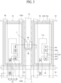
- Fig. 3 is an enlarged plan view illustrating a structure between two neighboring pixels arrayed as shown in Fig. 1 .
- Fig. 4 is a cross-sectional view along cutting line I-I' in Fig. 3 , for illustrating the electroluminescence display according to a preferred embodiment of the present disclosure.
- Fig. 3 shows the planar structure focusing on the circular part 'J' in Fig. 1 .
- one sub-pixel SP of the light emitting display may be defined by a scan line SL, a data line DL and a driving current line VDD.
- One sub-pixel SP of the light emitting display may include a switching thin film transistor ST, a driving thin film transistor DT, a light emitting diode OLE and a storage capacitance Cst.
- the driving current line VDD may be supplied with a high-level voltage for driving the light emitting diode OLE.
- a switching thin film transistor ST and a driving thin film transistor DT may be formed on a substrate SUB.
- the switching thin film transistor ST may be disposed at the portion where the scan line SL and the data line DL is crossing.
- the switching thin film transistor ST may include a switching gate electrode SG, a switching source electrode SS and a switching drain electrode SD.
- the switching gate electrode SG may be connected to the scan line SL, or be one portion of the scan line SL as shown in Fig. 3 .
- the switching source electrode SS may be connected to the data line DL and the switching drain electrode SD may be connected to the driving thin film transistor DT.
- the switching thin film transistor ST may play a role of selecting a pixel which would be driven.
- the driving thin film transistor DT may play a role of driving the light emitting diode OLE of the selected pixel by the switching thin film transistor ST.
- the driving thin film transistor DT may include a driving gate electrode DG, a driving source electrode DS and a driving drain electrode DD.
- the driving gate electrode DG may be connected to the switching drain electrode SD of the switching thin film transistor ST.
- the driving gate electrode DG may be connected to the switching drain electrode SD via the drain contact hole DH penetrating the gate insulating layer GI.
- the driving source electrode DS may be connected to the driving current line VDD, and the driving drain electrode DD may be connected to an anode electrode ANO of the light emitting diode OLE.
- a storage capacitance Cst may be disposed between the driving gate electrode DG of the driving thin film transistor DT and the anode electrode ANO of the light emitting diode OLE.
- the driving thin film transistor DT may be disposed between the driving current line VDD and the light emitting diode OLE.
- the driving thin film transistor DT may control the amount of electric currents flowing to the light emitting diode OLE from the driving current line VDD according to the voltage level of the driving gate electrode DG connected to the switching drain electrode SD of the switching thin film transistor ST.
- the light emitting diode OLE may include an anode electrode ANO, a light emitting layer EL and a cathode electrode CAT.
- the light emitting diode OLE may emit light according to the amount of the electric current contolled by the driving thin film transistor DT. In other word, the light emitting diode OLE may be driven by the voltage differences between the low-level voltage and the high-level voltage contolled by the driving thin film transistor DT.
- the anode electrode ANO of the light emitting diode OLE may be connected to the driving drain electrode DD of the driving thin film transistor DT, and the cathode electrode CAT may be connected to a low-level voltage line Vss where a low-level potential voltage is supplied. That is, the light emitting diode OLE may be driven by the high-level voltage controlled by the driving thin film transistor DT and the low-level voltage supplied from the low-level voltage line Vss.
- the semiconductor layers SA and DA may be formed on the substrate 110.
- the semiconductor layer may include a switching semiconductor layer SA of the switching thin film transistor ST and a driving semiconductor layer DA of the driving thin film transistor DT.
- the gate insulating layer GI is deposited on the semiconductor layer SA and DA to cover the entire substrate 110.
- the gate electrodes SG and DG may be formed on the gate insulating layer GI overlapped with the gate line SL and the semiconductor layers SA and DA.
- the gate electrode may include a switching gate electrode SG of the switching thin film transistor ST and a driving gate electrode DG of the driving thin film transistor DT.
- the swiching gate electrode SG may be branched from the gate line SL or may be defined as one portion of the gate line SL.
- the intermediate insulating layer ILD may be deposited on the gate line SL and the gate electrode SG and DG to cover the entire substrate 110.
- the source electrodes SS and DS, the drain electrodes SD and DD, the low-resistance line LL, the data line DL and the driving current line VDD may be disposed.
- the source electrodes may include a switching source electrode SS of the switching thin film transistor ST and a driving source electrode DS of the driving thin film transistor DT.
- the drain electrodes may include a switching drain electrode SD of the switching thin film transistor ST and a driving drain electrode DD of the driving thin film transistor DT.
- the source electrode SS and DS may contact one side of the semiconductor layer SA and DA via a contact hole penetrating the intermediate insulating layer ILD and the gate insulating layer GI.
- the drain electrode SD and DD may contact the other side of the semiconductor layer SA and DA via another contact hole penetrating the intermediate insulating layer ILD and the gate insulating layer GI.
- the switching source electrode SS may be branched from the data line DL.
- the switching drain electrode SD may be connected to the driving gate electrode DG and the driving thin film transistor DT.
- the driving source electrode DS may be branched from the driving current line VDD.
- the low-resistance line LL may be disposed between two neighboring pixel columns. In some cases, one low-resistance line LL may be disposed at every two or three pixel-columns.
- the low-resistance line LL may be connected to the cathode electrode CAT of the light emitting diode OLE. Otherwise, the low-resistance line LL may be connected to the low-voltage line VSS. In some cases, the low-resistance line LL may be the low-voltage line VSS.
- the passivation layer PAS may be deposited on the substrate 110 having the thin film transistors ST and DT.
- the passivation layer PAS may be made of an inorganic material including silicon oxide or silicon nitride.
- the planarization layer PL may be deposited on the passivation layer PAS.
- the planarization layer PL may be the thin film for flattening the non-uniform surface of the substrate 110 on which the thin film transistors ST and DT are formed. In order to make the uneven surface condition of the substrate 110, the planarization layer PL may be formed of an organic material.
- the passivation layer PAS and the planarization layer PL may include the pixel contact hole PH exposing some portions of the driving drain electrode DD of the driving thin film transistor DT.
- the anode electrode ANO may be formed on the planarization layer PL covering the thin film transistors ST and DT.
- the anode electrode ANO may be connected to the driving drain electrode DD of the driving thin film transistor DT through a pixel contact hole PH formed at the planarization layer PL.
- the anode electrode ANO may have various structures and different materials according to the emission type of the organic light emitting diode OLE. For example, for the bottom emission type in which the light may be provided to the substrate 110 direction from the emission layer EL, the anode electrode ANO may be made of a transparent conductive material.
- the anode electrode ANO of the bottom emission type may include oxide conductive material such as indium-zinc-oxide (or IZO) or indium-tin-oxide (or ITO).
- oxide conductive material such as indium-zinc-oxide (or IZO) or indium-tin-oxide (or ITO).
- ITO indium-tin-oxide
- the anode electrode ANO may be made of metal materials having excellent light reflectance.
- a bank BA may be formed on the anode electrode ANO.
- the bank BA may cover the circumference areas of the anode electrode ANO and may expose most of middle areas of the anode electrode ANO, so the bank BA may define the emission area.
- the bank BA may cover a portion of the top surface at the edge of the top surface and a corresponding portion of the side surface of the anode electrode ANO and may expose most of the middle area of the anode electrode ANO, so the bank BA may define the emission area as shown in fig. 4 .
- An emission layer EL may be deposited on the anode electrode ANO and the bank BA.
- the emission layer EL may be deposited over the entire surface of the display area DA on the substrate 110, covering the anode electrodes ANO and banks BA.
- the emission layer EL may include two or more stacked emission portions for emitting white light.
- the emission layer EL may include a first emission layer providing first color light and a second emission layer providing second color light, for emitting the white light by comining the first color light and the second color light.
- the emission layer EL may include any one of the blue emission layer, the green emission layer and the red emission layer for providing the light color corresponding to the color allocated at the pixel.
- the light emitting diode OLE may further include functional layers for enhancing the light emitting efficiency and/or life-time of the emission layer EL.
- the cathode electrode CAT may be disposed on the emission layer EL.
- the cathode electrode CAT may be stacked on the emission layer EL as being in surface contact with each other.
- the cathode electrode CAT may be formed as one sheet element over the entire area of the substrate 110 as being commonly connected whole emission layers EL disposed at all pixels.
- the cathode electrode CAT may include metal material having excellent light reflection ratio.
- the cathode electrode CAT may include at least any one of silver (Ag), aluminum (Al), molybdenum (Mo), titanium (Ti), copper (Cu), gold (Au), magnesium (Mg), calcium (Ca) or barium (Ba).
- the electroluminescence display according to the present disclosure may include a sub-pixel trench PLP which is formed by patterning the planarization layer PL.
- the sub-pixel trench PLP may be disposed as surrounding each of the sub-pixel, so that it may distinguish any one sub-pixel SP form the neighboring sub-pixel SP.
- On the planarization layer PL surrounded by the sub-pixel trench PLP there is one of: the anode electrode ANO and/or the bank BA.
- the bank BA may be disposed between end of the anode electrode ANO and end of the planarization layer PL surrounded by the sub-pixel trench PLP. That is, the bank BA may have a structure of patterned along the circumference area of the anode electrode ANO.
- 'sub-pixel trench' is referred when a sub-pixel is used as a basic unit.
- a 'sub-pixel' may be referred to as a 'pixel' and a 'pixel' is described as a basic unit, it may be referred to as a 'pixel trench'.
- the electroluminescence display according to the present disclosure may include a cathode contact hole CON for connecting the low-resistance line LL and the cathode electrode CAT.
- the cathod contact hole CON may be formed by penetrating the passivation layer PAS and the planarization layer PL covering the low-resistance line LL.
- the passivation layer PAS stacked under the planarization layer PL may have an under-cut profile formed by being over-etched than the planarization layer PL.
- the emission layer EL may be deposited only at a middle area of the low-resistance line LL exposed by the cathode contact hole CON.
- the emission layer EL may include an organic material.
- the emission layer EL may not be stacked on the etched side wall at the under-cut area, but on some of the exposed area of the surface. Since this stacked portion is not connected to the emission layer EL, it is referred to as a 'dummy emission layer DEL'.
- the cathode electrode CAT stacked on the emission layer EL may be also stacked from the under-cut portion to the etched side wall and the top surface. As a result, the cathode electrode CAT may extend from one pixel P1 through the cathode contact hole CON to the neighboring pixel P2, and then may be connected to the low-resistance line LL.
- the electroluminescence display according to the present disclosure may include an under-cut trench TR between cathode contact hole CON and the bank BA.
- the under-cut trench TR may be an element for preventing the end portion of the planarization layer PL from being damaged at the under-cut portion forming the cathode contact hole CON.
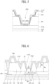
- Fig. 5 is an enlarged cross-sectional view of the circular part 'M' in Fig. 4 .
- Fig. 6 is an enlarged cross-sectional view of the circular part 'N' in Fig. 4 .
- the functional layer which is a part of the emission layer may be formed as a common layer covering the entire surface of the substrate.
- the hole injection layer and the hole transport layer stacked just over the anode electrode ANO, and the electron injection layer and the electron transport layer stacked just under the cathode electrode CAT may be formed as a continuous common layer covering the banks BA and the sub-pixels SP. That is, most of the emission layer EL may be stacked on all of the display area DA of the substrate 110.
- pixel density unit, PPI: Pixel Per Inch
- PPI Pixel Per Inch
- the size of the pixel P becomes smaller, and the distance between the neighboring pixels P becomes narrower.
- electrons or charges may move in a lateral direction through the functional layers connecting between the neighboring sub-pixels SP, thereby affecting the function and/or operation of the neighboring sub-pixel SP.
- This flow of the electrons or charges between neighboring sub-pixels SP may be defined as lateral leakage current (or LLC).
- lateral leakage current increases, color information of an image may be distorted and thus image quality may be deteriorated.
- the electroluminescence display according to the present disclosure may further include a sub-pixel trench PLP formed by removing some parts of the planarization layer PL, so as to distinguish each sub-pixel SP.
- the passivation layer PAS stacked under the planarization layer PL may be exposed through the sub-pixel trench PLP.
- the sub-pixel trench PLP may have a depth lower than the thickness of the planarization layer PL so that the passivation layer PAS may not be exposed.
- the emission layer EL stacked on this portion may have longer path of current between neighboring sub-pixels SP.
- the path of the lateral leakage current along the functional layers connected between the neighboring sub-pixels SP may become longer.
- the lateral leakage current transferred from one sub-pixel SP to the neighboring sub-pixel SP may be suppressed, thereby preventing image quality from being deteriorated.
- the thickness of the emission layer EL stacked on the etched sidewall may decrease. In this case, the electrical resistance may be increased in the emission layer EL through which the lateral leakage current is transmitted so that the lateral leakage current may not be easily flow.
- the cathode electrode CAT may be preferably formed of a transparent conductive material such as ITO (Indium-Tin-Oxide) or IZO(Indium-Zinc-Oxide). ITO and IZO may have relatively high sheet resistance than that of metal materials. As the sheet resistance of the cathode electrode is increased, the voltage of the cathode electrode may not be constantly maintained over the entire display screen, and thus image quality may be non-uniformed.
- ITO Indium-Tin-Oxide
- IZO Indium-Zinc-Oxide
- the ultra-high-resolution large area electroluminescence display it may be preferable to have a top emission type capable of ensuring a light emitting area enough to have same luminance with lower power consumption. Accordingly, in the ultra-high-resolution large area electroluminescence display, it is preferable to include a low resistance line LL for lowering the sheet resistance of the cathode electrode.
- the low resistance line LL may be connected to the cathode electrode CAT stacked on the emission layer EL to lower the sheet resistance of the cathode electrode CAT.
- the electroluminescence display may include a cathode contact hole CON at the planarization layer PL on which the light emitting diode OLE may be disposed.
- the cathode contact hole CON may expose some portions of the low resistance line LL by removing some portions of the passivation layer PAS and the planarization layer PL covering the low resistance line LL.
- the passivation layer PAS may have a first aperture OA1 having a first width W1.
- the planarization layer PL may have a second aperture OA2 having a second width W2. Further, the first width W1 may be wider than the second width W2, and the first aperture OA1 and the second aperture OA2 are disposed so that their center points are overlapped each other.
- the cathode contact hole CON may be formed after the anode electrode ANO is patterned, the bank BA is formed, the planarization layer PL exposed between the banks BA is patterned, and then the passivation layer PAS is etched.
- the passivation layer PAS may be over-etched to form the first aperture OA1 wider than the second aperture OA2 formed at the planarization layer PL.
- the cathode contact hole COM may be formed as having the under-cut structure.
- the emission layer EL may be deposited on the substrate 110 as covering whole of the display area DA.
- the emission layer EL may be formed of an organic material.
- the emission layer EL may be stacked only on the area vertically exposed by the cathode contact hole CON. Meanwhile, in the cathode contact hie CON, the emission layer EL may be only partially stacked on the inclined side wall which is formed by etching of the planarization layer PL.
- the emission layer EL may be disconnected at the cathode contact hole CON by the under-cut structure of the cathode contact hole CON.
- the cathode electrode CAT may be deposited on the emission layer EL as covering the entire surface of the substrate 110.
- the cathode electrode CAT may be formed of a transparent conductive material such as ITO or IZO. These transparent conductive materials may be inorganic materials, and when it is stacked on a stepped surface, the step-coverage is very excellent.
- the cathode electrode may be deposited along the etched sidewall even inside the cathode contact hole CON having an under-cut structure. Since the cathode electrode CAT is stacked while covering all inside surfaces of the cathode contact hole CON as shown in Fig. 6 , it has a continuous structure over the entire area of the substrate 110 without disconnection.
- the cathode electrode CAT may contact the low resistance line LL exposed by the cathode contact hole CON. That is, since the emission layer EL does not completely cover the surface of the low resistance line LL exposed to the cathode contact hole CON, the cathode electrode CAT is connected to the low resistance line LL.
- the under-cut trench TR may be formed at the planarization layer PL disposed between the bank BA and the cathode contact hole CON.
- the under-cut trench TR may be an element provided to completely maintain the structure of the cathode contact hole CON having the under-cut structure.
- the under-cut trench TR may be a trench formed by removing a partial thickness of the planarization layer PL.
- Ha: Hb which is a ratio of the thickness Ha of the planarization layer PL to the depth Hb of the under-cut trench TR, may have a value greater than or equal to 4:3.
- the depth Hb of the under-cut trench TR may be equal to or smaller than the thickness Ha of the maximum planarization layer PL. That is, the ratio relationship between the depth Hb of the under-cut trench TR and the thickness Ha of the planarization layer PL may be selected from any one value within the range of 4:3 ⁇ Ha:Hb ⁇ 1:1.
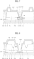
- Fig. 7 is an enlarged cross-sectional view illustrating a structure of the electroluminescence display without the under-cut trench according to the present disclosure.
- Fig. 7 shows the cross-sectional structure of the cathode contact hole CON, in the case that the under-cut trench TR is not formed around the cathode contact hole CON.
- the first aperture OA1 is formed by patterning the passivation layer PAS to form a cathode contact hole CON.
- the end of the planarization layer PL may be lifted upward from the horizontal direction. This may occur because the bank BA does not completely cover the entire planarization layer PL, but covers only a partial area of the planarization layer PL. It may be caused by a phenomenon in which the etched end of the planarization layer PL is shrunk during a heat treatment process that may be performed in the over-etching process.
- the emission layer EL when the emission layer EL is deposited, the emission layer EL may be stacked along the etched sidewall of the cathode contact hole CON. As the result, all of the low resistance line LL exposed to the cathode contact hole CON may be covered by the emission layer EL. Further, since the cathode electrode CAT is subsequently stacked on the emission layer EL, the cathode electrode CAT may not be connected to the low resistance line LL.
- the thermal stress applied to the planarization layer PL may be distributed through the under-cut trench TR.
- a phenomenon in which the etched end of the planarization layer PL is lifted may not be occurred.
- the emission layer EL may expose most of the low resistance line LL in the cathode contact hole CON.
- the cathode electrode CAT when the cathode electrode CAT is deposited, the cathode electrode CAT may be physically and electrically connected to the low resistance line LL.
- FIG. 8 is a cross-sectional view illustrating the structure of the under-cut trench according to another example of the present disclosure.
- the under-cut trench TR according to another example may have a structure completely filled by the bank BA.
- the under-cut trench TR may be disposed between the anode electrode ANO and the cathode contact hole CON.
- the bank BA may be preferably formed to have a smaller width than the planarization layer PL exposed outside the anode electrode ANO.
- the bank BA may be spaced apart from the end of the planarization layer PL by a predetermined distance L inwardly.
- Fig. 9 is an enlarged cross-sectional view illustrating a structure in which a bank and a planarization layer are formed in the same pattern in the electroluminescence display according to the present disclosure.
- the etched sidewall W forming the cathode contact hole CON may have a very steep slope, and the slope length of the sidewall may be also relatively long.
- the etched sidewall W of the cathode contact hole CON may have a length corresponding to the sum of the thickness of the bank BA and the thickness of the planarization layer PL.
- the entire etched sidewall W may not be covered.
- the emission layer EL may include organic material.
- the amount of the deposited of the emission layer EL on the etched sidewall W may be very small.
- the cathode electrode CAT which includes inorganic material may not cover the entire etched sidewall W, and its connectivity may be cut off. As a result, the cathode electrode CAT and the low resistance line LL may not be completely connected in the cathode contact hole CON.
- the bank BA does not completely cover the planarization layer PL, but the bank BA exposes some portions of the planarization layer PL, as shown in Figs. 6 and 8 .
- the bank BA covers the under-cut trench TR, it is preferable not to completely cover the planarization layer PL.
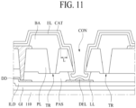
- Fig. 10 is a cross-sectional view illustrating a structure of the under-cut trench according to another embodiment of the present disclosure.
- the under-cut trench TR according to another embodiment of the present disclosure may have the same depth as the thickness of the planarization layer PL.
- the depth of the under-cut trench TR may be etched corresponding to the same thickness of the planarization layer PL.
- the bank BA may be formed to completely fill the under-cut trench TR.
- the under-cut trench TR may be disposed between the anode electrode ANO and the cathode contact hole CON. Even in this structure, when the cathode contact hole CON having an under-cut structure is formed, the problem that the etched end of the planarization layer PL is lifted may not occur.
- the bank BA is preferably formed to have a smaller width than the planarization layer PL exposed outside the anode electrode ANO.
- the bank BA is preferable to form the bank BA to be spaced apart from the end of the planarization layer PL by a predetermined distance L inward.
- FIG. 12 is a plane view illustrating a structure of the electroluminescence display according to another embodiment of the present disclosure.
- the electroluminescence display shown in Fig. 12 may be a diagram illustrating a case in which the pixel density is very high.
- all sub-pixels SP disposed in the display area DA may be uniformly spaced apart.
- an interval between the pixels P may not be specifically defined.
- a low resistance line LL may be disposed between the plurality of sub-pixel columns.
- a cathode contact hole CON may be formed on the low resistance line LL, and the cathode electrode CAT and the low resistance line LL may be connected via the cathode contact hole CON.
- the spacing between the sub-pixels SP is very narrow, it may not be easy to form the cathode contact hole CON.
- the cathode contact hole CON may be formed at the intersection area K where four neighboring pixels P are adjacent.
- a cathode contact hole CON may be formed at the intersection area K where the white sub-pixel SPW of the first pixel P1, the red sub-pixel SPR of the second pixel P2, the white sub-pixel SPW of the third pixel P3 and the red sub-pixel SPR of the fourth pixel P4 intersect.
- the areas corresponding to the intersection portions of the four sub-pixels SP may be partially removed to ensure the square intersection area K.
- planarization layer PL and the passivation layer PAS may be patterned in the square intersection area K to form a cathode contact hole CON exposing the low resistance line LL disposed there-under.
- the electroluminescence display according to the present disclosure may include a structure in which the low resistance line LL is disposed between two adjacent sub-pixels SP of two neighboring pixels P, and a cathode contact hole CON is disposed for exposing some portions of the low resistance line LL.
- the patterns for forming the cathode contact hole CON may be disposed as overlapping the sub-pixel trench PLP disposed between two anode electrodes ANO disposed at both sides. In other words, the cathode contact hole may overlap the low resistance line in the pixel trench.
- Fig. 3 in order to clearly show the structure of the cathode contact hole CON, it is illustrated as having a shape protruding from the planarization layer PL on both sides. Meanwhile, the cathode contact hole CON may be formed by arranging the planarization layer PL on both sides without a protruding shape, and etching only the passivation layer PAS exposed there-between.
- Fig. 12 shows a structure in which the low resistance line LL is disposed with a higher resolution.
- Fig. 12 shows the structure in which the cathode contact hole CON is disposed by forming partially removed regions inside each sub-pixel SP at the portion where the four sub-pixels SP are arranged.
Landscapes
- Engineering & Computer Science (AREA)
- Microelectronics & Electronic Packaging (AREA)
- Physics & Mathematics (AREA)
- Geometry (AREA)
- Electroluminescent Light Sources (AREA)
- Devices For Indicating Variable Information By Combining Individual Elements (AREA)
Applications Claiming Priority (1)
| Application Number | Priority Date | Filing Date | Title |
|---|---|---|---|
| KR1020210177811A KR102959069B1 (ko) | 2021-12-13 | 전계 발광 표시장치 |
Publications (1)
| Publication Number | Publication Date |
|---|---|
| EP4195902A1 true EP4195902A1 (de) | 2023-06-14 |
Family
ID=83457239
Family Applications (1)
| Application Number | Title | Priority Date | Filing Date |
|---|---|---|---|
| EP22197692.1A Pending EP4195902A1 (de) | 2021-12-13 | 2022-09-26 | Elektrolumineszenzanzeige |
Country Status (3)
| Country | Link |
|---|---|
| US (1) | US20230189572A1 (de) |
| EP (1) | EP4195902A1 (de) |
| CN (1) | CN116264795A (de) |
Cited By (1)
| Publication number | Priority date | Publication date | Assignee | Title |
|---|---|---|---|---|
| WO2025020744A1 (zh) * | 2023-07-27 | 2025-01-30 | 京东方科技集团股份有限公司 | 显示面板、其制作方法及显示装置 |
Citations (3)
| Publication number | Priority date | Publication date | Assignee | Title |
|---|---|---|---|---|
| KR20170078969A (ko) * | 2015-12-29 | 2017-07-10 | 엘지디스플레이 주식회사 | 유기전계발광표시 장치 및 이의 제조방법 |
| KR20180013226A (ko) * | 2016-07-29 | 2018-02-07 | 엘지디스플레이 주식회사 | 유기 발광 표시 장치 및 그 제조 방법 |
| EP3761366A1 (de) * | 2019-07-05 | 2021-01-06 | Samsung Display Co., Ltd. | Anzeigevorrichtung |
Family Cites Families (1)
| Publication number | Priority date | Publication date | Assignee | Title |
|---|---|---|---|---|
| KR102593461B1 (ko) * | 2018-10-19 | 2023-10-24 | 엘지디스플레이 주식회사 | 유기 발광 표시 장치 |
-
2022
- 2022-07-19 US US17/868,620 patent/US20230189572A1/en active Pending
- 2022-08-01 CN CN202210915703.1A patent/CN116264795A/zh active Pending
- 2022-09-26 EP EP22197692.1A patent/EP4195902A1/de active Pending
Patent Citations (3)
| Publication number | Priority date | Publication date | Assignee | Title |
|---|---|---|---|---|
| KR20170078969A (ko) * | 2015-12-29 | 2017-07-10 | 엘지디스플레이 주식회사 | 유기전계발광표시 장치 및 이의 제조방법 |
| KR20180013226A (ko) * | 2016-07-29 | 2018-02-07 | 엘지디스플레이 주식회사 | 유기 발광 표시 장치 및 그 제조 방법 |
| EP3761366A1 (de) * | 2019-07-05 | 2021-01-06 | Samsung Display Co., Ltd. | Anzeigevorrichtung |
Cited By (1)
| Publication number | Priority date | Publication date | Assignee | Title |
|---|---|---|---|---|
| WO2025020744A1 (zh) * | 2023-07-27 | 2025-01-30 | 京东方科技集团股份有限公司 | 显示面板、其制作方法及显示装置 |
Also Published As
| Publication number | Publication date |
|---|---|
| KR20230089293A (ko) | 2023-06-20 |
| US20230189572A1 (en) | 2023-06-15 |
| CN116264795A (zh) | 2023-06-16 |
Similar Documents
| Publication | Publication Date | Title |
|---|---|---|
| KR102717811B1 (ko) | 유기 발광 표시 장치 | |
| US10403845B2 (en) | Top-emissive organic light-emitting diode display | |
| US10431768B2 (en) | Organic light-emitting display device including auxiliary electrode | |
| US12185617B2 (en) | Display cell and display device with power line having slit pattern in cut-off area | |
| EP4203651A1 (de) | Elektrolumineszenzanzeige | |
| EP4203659B1 (de) | Elektrolumineszenzanzeige mit reparaturstruktur und verfahren zur herstellung davon | |
| US20250280724A1 (en) | Electroluminescence Display | |
| US12446410B2 (en) | Electroluminescence display | |
| EP4195902A1 (de) | Elektrolumineszenzanzeige | |
| US20230200193A1 (en) | Electroluminescence display | |
| US20240188362A1 (en) | Light emitting display device | |
| US12538648B2 (en) | Top emission type electroluminescence display with reduced distance between anode and cathode | |
| KR102959069B1 (ko) | 전계 발광 표시장치 | |
| US20260123241A1 (en) | Light emitting display device | |
| US20250081746A1 (en) | Light emitting display device | |
| US20240224623A1 (en) | Electroluminescence display | |
| US20230209917A1 (en) | Bottom emission type electroluminescence display | |
| US20250194302A1 (en) | Display device | |
| US20240260313A1 (en) | Light emitting display device | |
| US20240260361A1 (en) | Light emitting display device |
Legal Events
| Date | Code | Title | Description |
|---|---|---|---|
| PUAI | Public reference made under article 153(3) epc to a published international application that has entered the european phase |
Free format text: ORIGINAL CODE: 0009012 |
|
| STAA | Information on the status of an ep patent application or granted ep patent |
Free format text: STATUS: REQUEST FOR EXAMINATION WAS MADE |
|
| 17P | Request for examination filed |
Effective date: 20220926 |
|
| AK | Designated contracting states |
Kind code of ref document: A1 Designated state(s): AL AT BE BG CH CY CZ DE DK EE ES FI FR GB GR HR HU IE IS IT LI LT LU LV MC MK MT NL NO PL PT RO RS SE SI SK SM TR |
|
| RBV | Designated contracting states (corrected) |
Designated state(s): AL AT BE BG CH CY CZ DE DK EE ES FI FR GB GR HR HU IE IS IT LI LT LU LV MC MK MT NL NO PL PT RO RS SE SI SK SM TR |
|
| STAA | Information on the status of an ep patent application or granted ep patent |
Free format text: STATUS: EXAMINATION IS IN PROGRESS |
|
| 17Q | First examination report despatched |
Effective date: 20250228 |