EP4195398A1 - Printed circuit board (pcb) assembly and electronic device - Google Patents
Printed circuit board (pcb) assembly and electronic device Download PDFInfo
- Publication number
- EP4195398A1 EP4195398A1 EP22847104.1A EP22847104A EP4195398A1 EP 4195398 A1 EP4195398 A1 EP 4195398A1 EP 22847104 A EP22847104 A EP 22847104A EP 4195398 A1 EP4195398 A1 EP 4195398A1
- Authority
- EP
- European Patent Office
- Prior art keywords
- battery
- conductor
- groove area
- pcb
- disposed
- Prior art date
- Legal status (The legal status is an assumption and is not a legal conclusion. Google has not performed a legal analysis and makes no representation as to the accuracy of the status listed.)
- Granted
Links
Images



Classifications
-
- H—ELECTRICITY
- H01—ELECTRIC ELEMENTS
- H01M—PROCESSES OR MEANS, e.g. BATTERIES, FOR THE DIRECT CONVERSION OF CHEMICAL ENERGY INTO ELECTRICAL ENERGY
- H01M50/00—Constructional details or processes of manufacture of the non-active parts of electrochemical cells other than fuel cells, e.g. hybrid cells
- H01M50/50—Current conducting connections for cells or batteries
- H01M50/502—Interconnectors for connecting terminals of adjacent batteries; Interconnectors for connecting cells outside a battery casing
-
- H—ELECTRICITY
- H01—ELECTRIC ELEMENTS
- H01M—PROCESSES OR MEANS, e.g. BATTERIES, FOR THE DIRECT CONVERSION OF CHEMICAL ENERGY INTO ELECTRICAL ENERGY
- H01M10/00—Secondary cells; Manufacture thereof
- H01M10/42—Methods or arrangements for servicing or maintenance of secondary cells or secondary half-cells
- H01M10/425—Structural combination with electronic components, e.g. electronic circuits integrated to the outside of the casing
-
- H—ELECTRICITY
- H01—ELECTRIC ELEMENTS
- H01M—PROCESSES OR MEANS, e.g. BATTERIES, FOR THE DIRECT CONVERSION OF CHEMICAL ENERGY INTO ELECTRICAL ENERGY
- H01M50/00—Constructional details or processes of manufacture of the non-active parts of electrochemical cells other than fuel cells, e.g. hybrid cells
- H01M50/20—Mountings; Secondary casings or frames; Racks, modules or packs; Suspension devices; Shock absorbers; Transport or carrying devices; Holders
- H01M50/284—Mountings; Secondary casings or frames; Racks, modules or packs; Suspension devices; Shock absorbers; Transport or carrying devices; Holders with incorporated circuit boards, e.g. printed circuit boards [PCB]
-
- H—ELECTRICITY
- H01—ELECTRIC ELEMENTS
- H01M—PROCESSES OR MEANS, e.g. BATTERIES, FOR THE DIRECT CONVERSION OF CHEMICAL ENERGY INTO ELECTRICAL ENERGY
- H01M50/00—Constructional details or processes of manufacture of the non-active parts of electrochemical cells other than fuel cells, e.g. hybrid cells
- H01M50/50—Current conducting connections for cells or batteries
- H01M50/502—Interconnectors for connecting terminals of adjacent batteries; Interconnectors for connecting cells outside a battery casing
- H01M50/514—Methods for interconnecting adjacent batteries or cells
-
- H—ELECTRICITY
- H01—ELECTRIC ELEMENTS
- H01M—PROCESSES OR MEANS, e.g. BATTERIES, FOR THE DIRECT CONVERSION OF CHEMICAL ENERGY INTO ELECTRICAL ENERGY
- H01M50/00—Constructional details or processes of manufacture of the non-active parts of electrochemical cells other than fuel cells, e.g. hybrid cells
- H01M50/50—Current conducting connections for cells or batteries
- H01M50/502—Interconnectors for connecting terminals of adjacent batteries; Interconnectors for connecting cells outside a battery casing
- H01M50/519—Interconnectors for connecting terminals of adjacent batteries; Interconnectors for connecting cells outside a battery casing comprising printed circuit boards [PCB]
-
- H—ELECTRICITY
- H05—ELECTRIC TECHNIQUES NOT OTHERWISE PROVIDED FOR
- H05K—PRINTED CIRCUITS; CASINGS OR CONSTRUCTIONAL DETAILS OF ELECTRIC APPARATUS; MANUFACTURE OF ASSEMBLAGES OF ELECTRICAL COMPONENTS
- H05K1/00—Printed circuits
- H05K1/18—Printed circuits structurally associated with non-printed electric components
-
- H—ELECTRICITY
- H05—ELECTRIC TECHNIQUES NOT OTHERWISE PROVIDED FOR
- H05K—PRINTED CIRCUITS; CASINGS OR CONSTRUCTIONAL DETAILS OF ELECTRIC APPARATUS; MANUFACTURE OF ASSEMBLAGES OF ELECTRICAL COMPONENTS
- H05K1/00—Printed circuits
- H05K1/18—Printed circuits structurally associated with non-printed electric components
- H05K1/182—Printed circuits structurally associated with non-printed electric components associated with components mounted in printed circuit boards [PCB], e.g. insert-mounted components [IMC]
- H05K1/183—Printed circuits structurally associated with non-printed electric components associated with components mounted in printed circuit boards [PCB], e.g. insert-mounted components [IMC] associated with components mounted in and supported by recessed areas of the PCBs
-
- H—ELECTRICITY
- H05—ELECTRIC TECHNIQUES NOT OTHERWISE PROVIDED FOR
- H05K—PRINTED CIRCUITS; CASINGS OR CONSTRUCTIONAL DETAILS OF ELECTRIC APPARATUS; MANUFACTURE OF ASSEMBLAGES OF ELECTRICAL COMPONENTS
- H05K3/00—Apparatus or processes for manufacturing printed circuits
- H05K3/30—Assembling printed circuits with electric components, e.g. with resistors
- H05K3/32—Assembling printed circuits with electric components, e.g. with resistors electrically connecting electric components or wires to printed circuits
- H05K3/328—Assembling printed circuits with electric components, e.g. with resistors electrically connecting electric components or wires to printed circuits by welding
-
- H—ELECTRICITY
- H05—ELECTRIC TECHNIQUES NOT OTHERWISE PROVIDED FOR
- H05K—PRINTED CIRCUITS; CASINGS OR CONSTRUCTIONAL DETAILS OF ELECTRIC APPARATUS; MANUFACTURE OF ASSEMBLAGES OF ELECTRICAL COMPONENTS
- H05K2201/00—Indexing scheme relating to printed circuits covered by H05K1/00
- H05K2201/09—Shape and layout
- H05K2201/09009—Substrate related
- H05K2201/09036—Recesses or grooves in insulating substrate
-
- H—ELECTRICITY
- H05—ELECTRIC TECHNIQUES NOT OTHERWISE PROVIDED FOR
- H05K—PRINTED CIRCUITS; CASINGS OR CONSTRUCTIONAL DETAILS OF ELECTRIC APPARATUS; MANUFACTURE OF ASSEMBLAGES OF ELECTRICAL COMPONENTS
- H05K2201/00—Indexing scheme relating to printed circuits covered by H05K1/00
- H05K2201/09—Shape and layout
- H05K2201/09209—Shape and layout details of conductors
- H05K2201/09372—Pads and lands
- H05K2201/09472—Recessed pad for surface mounting; Recessed electrode of component
-
- H—ELECTRICITY
- H05—ELECTRIC TECHNIQUES NOT OTHERWISE PROVIDED FOR
- H05K—PRINTED CIRCUITS; CASINGS OR CONSTRUCTIONAL DETAILS OF ELECTRIC APPARATUS; MANUFACTURE OF ASSEMBLAGES OF ELECTRICAL COMPONENTS
- H05K2201/00—Indexing scheme relating to printed circuits covered by H05K1/00
- H05K2201/10—Details of components or other objects attached to or integrated in a printed circuit board
- H05K2201/10007—Types of components
- H05K2201/10037—Printed or non-printed battery
-
- H—ELECTRICITY
- H05—ELECTRIC TECHNIQUES NOT OTHERWISE PROVIDED FOR
- H05K—PRINTED CIRCUITS; CASINGS OR CONSTRUCTIONAL DETAILS OF ELECTRIC APPARATUS; MANUFACTURE OF ASSEMBLAGES OF ELECTRICAL COMPONENTS
- H05K2201/00—Indexing scheme relating to printed circuits covered by H05K1/00
- H05K2201/10—Details of components or other objects attached to or integrated in a printed circuit board
- H05K2201/10613—Details of electrical connections of non-printed components, e.g. special leads
-
- Y—GENERAL TAGGING OF NEW TECHNOLOGICAL DEVELOPMENTS; GENERAL TAGGING OF CROSS-SECTIONAL TECHNOLOGIES SPANNING OVER SEVERAL SECTIONS OF THE IPC; TECHNICAL SUBJECTS COVERED BY FORMER USPC CROSS-REFERENCE ART COLLECTIONS [XRACs] AND DIGESTS
- Y02—TECHNOLOGIES OR APPLICATIONS FOR MITIGATION OR ADAPTATION AGAINST CLIMATE CHANGE
- Y02E—REDUCTION OF GREENHOUSE GAS [GHG] EMISSIONS, RELATED TO ENERGY GENERATION, TRANSMISSION OR DISTRIBUTION
- Y02E60/00—Enabling technologies; Technologies with a potential or indirect contribution to GHG emissions mitigation
- Y02E60/10—Energy storage using batteries
Definitions
- This application relates to the field of terminal technologies, and in particular, to a printed circuit board PCB assembly and an electronic device.
- dual batteries are increasingly used in the industry as an apparatus for supplying power to terminal devices.
- a steel sheet is usually installed on a surface of a printed circuit board (Printed-circuit Board, PCB), and serves as a power cable for connecting two battery negative electrodes. It should be noted that the thicker and wider the conductor, the smaller its impedance. Therefore, a width of a steel sheet that serves as a power cable is usually greater than a preset width threshold. As more and more components are used on the PCB, a steel sheet mounted on a surface occupies a relatively large area on the PCB, and consequently. an area of another component that can be installed on the PCB is reduced.
- PCB printed circuit Board
- Embodiments of this application provide a printed circuit board PCB assembly and an electronic device, so as to reduce an area proportion of a power cable connecting two battery negative electrodes on a PCB.
- a printed circuit board PCB assembly where the PCB assembly includes a PCB, a first conductor, a first battery, and a second battery; the PCB includes a groove area;
- the PCB assembly includes a PCB, a first conductor, a first battery, and a second battery.
- the PCB includes a groove area.
- the first battery and the second battery are disposed on different sides of the groove area.
- the first conductor is disposed in the groove area, and the first conductor is configured to connect the first battery and the second battery. That is, in this embodiment of this application, the first battery and the second battery are connected by using the first conductor in the groove area, thereby preventing a power cable connecting the first battery and the second battery from occupying an area on the PCB, and increasing an area in which other components can be installed on the PCB.
- the PCB component further includes a target component, the target component is a component disposed in the groove area, and the first conductor is a bracket that fastens the target component to the groove area.
- the PCB assembly provided in this embodiment of this application includes a PCB, a first conductor, a first battery, and a second battery, and a target component.
- the PCB includes a groove area.
- the first battery and the second battery are disposed on different sides of the groove area.
- the first conductor is disposed in the groove area, and the first conductor is a bracket that fastens the target component to the groove area, and is configured to connect the first battery and the second battery.
- the target component is a component disposed in the groove area.
- the first conductor that is configured to connect the first battery and the second battery is a reused bracket that fastens the target component to the groove area, thereby further reducing an area occupied by the power cable connecting the first battery and the second battery on the PCB, reducing costs of the PCB assembly, and increasing an area in which other components can be installed on the PCB.
- the PCB assembly further includes an insulating material, and the insulating material is disposed between the first conductor and the target component.
- disposing the insulating material between the first conductor and the target component can avoid short circuit between the target component and the first battery and the second battery.
- the target component is a camera module.
- the target component is a camera module
- the first conductor that is configured to connect the first battery and the second battery reuses the bracket that fastens the target component to the groove area, thereby further reducing an area occupied by the power cable connecting the first battery and the second battery on the PCB, reducing costs of the PCB assembly, and increasing an area in which other components can be installed on the PCB.
- the PCB assembly when a distance between the first battery and the groove area is greater than a preset distance threshold, the PCB assembly further includes a second conductor, the second conductor is disposed between the first battery and the groove area, and the second conductor is configured to connect the first conductor and the first battery; and/or when a distance between the second battery and the groove area is greater than the preset distance threshold, the PCB assembly further includes a third conductor, the third conductor is disposed between the second battery and the groove area, and the third conductor is configured to connect the first conductor and the second battery.
- the PCB assembly includes a PCB, a first conductor, a first battery, a second battery, a target component, and a second conductor.
- the PCB includes a groove area.
- the first battery and the second battery are disposed on different sides of the groove area.
- the first conductor is disposed in the groove area.
- the target component is a component disposed in the groove area.
- the first conductor is also a bracket that fastens the target component to the groove area.
- a distance between the first battery and the groove area is greater than a preset distance threshold.
- the second conductor is disposed between the first battery and the groove area. The second conductor is connected to the first battery and the second battery by using the first conductor and the second conductor.
- the first battery may be disposed in a position far away from the groove area, and does not need to be disposed close to the groove area.
- the first battery and the second battery may be connected by using the first conductor and the second conductor, thereby improving flexibility of the disposing position of the first battery.
- a width of each of the first conductor, the second conductor, and the third conductor is greater than a preset width threshold.
- the first conductor is fastened to the groove area by using a welding method.
- the first conductor is fastened to the groove area by using a welding method. Only a relatively small pad needs to be disposed on the PCB, so that the first conductor can be fastened to the groove area. This further reduces an area occupied by the power cable of the first battery and the second battery on the PCB, and increases an area in which other components can be installed on the PCB.
- an electronic device includes a printed circuit board PCB assembly, and the PCB assembly includes a PCB, a first conductor, a first battery, and a second battery; the PCB includes a groove area; the first battery and the second battery are disposed on different sides of the groove area; and the first conductor is disposed in a groove area, and the first conductor is configured to connect the first battery and the second battery.
- the PCB component further includes a target component, the target component is a component disposed in the groove area, and the first conductor is a bracket that fastens the target component to the groove area.
- the PCB assembly further includes an insulating material, and the insulating material is disposed between the first conductor and the target component.
- the PCB assembly when a distance between the first battery and the groove area is greater than a preset distance threshold, the PCB assembly further includes a second conductor, the second conductor is disposed between the first battery and the groove area, and the second conductor is configured to connect the first conductor and the first battery; and/or when a distance between the second battery and the groove area is greater than the preset distance threshold, the PCB assembly further includes a third conductor, the third conductor is disposed between the second battery and the groove area, and the third conductor is configured to connect the first conductor and the second battery.
- a width of each of the first conductor, the second conductor, and the third conductor is greater than a preset width threshold.
- the first conductor is fastened to the groove area by using a welding method.
- first”, “second”, and “third” are used for descriptive purposes only, and cannot be construed as indicating or implying relative importance or implicitly indicating the quantity of technical features indicated. Therefore, the features defined with “first”, “second” and “third” may explicitly or implicitly include one or more of the features.
- a PCB assembly provided in embodiments of this application may be applied to an electronic device.
- the electronic device may be a laptop computer, a tablet computer, a palmtop computer, a vehicle-mounted terminal, a point of sales terminal, a wearable device, a mobile phone, or the like.
- a power cable connecting two battery negative electrodes may be a steel sheet, and the steel sheet may be attached to a surface of the PCB by using a surface mounted technology (Surface Mounted Technology, SMT).
- SMT Surface Mounted Technology
- the steel sheet is grounded by using a precision detection resistor, and the precision detection resistor may be configured to detect a current value on the steel sheet.
- impedance of the power cable connecting two battery negative electrodes is lower than a preset impedance threshold (for example, 2 mohms). The wider the conductor is, the lower the impedance is. Therefore, a width of the steel sheet is relatively large.
- the PCB assembly includes a PCB, a first battery, a second battery, and a first conductor.
- the first conductor is a conductor disposed in the groove area, and may be configured to support a component disposed in the groove area.
- the first battery and the second battery are disposed on different sides of the groove area. For example, as shown in (a) in FIG. 2 , the first battery is disposed on a left side of the groove area, and the second battery is disposed on a right side of the groove area. As shown in (b) in FIG.
- the first conductor in the groove area is reused as a power cable that connects the first battery and the second battery, so that the power cable that connects the first battery and the second battery does not need to occupy an additional area of the PCB, thereby increasing an of an component-installable area on the PCB.
- an embodiment of this application provides a PCB assembly 1000, and the PCB assembly 1000 includes a PCB 1100, a first conductor 1200, a first battery 1300, and a second battery 1400.
- the PCB 1100 includes a groove area 1101.
- the first battery 1300 and the second battery 1400 are disposed on different sides of the groove area 1101.
- the first conductor 1200 is disposed in a groove area 1101, and the first conductor 1200 is configured to connect the first battery 1300 and the second battery 1400.
- FIG. 3 is a top view of the PCB assembly 1000 according to an embodiment of this application, and (b) in FIG. 3 is a side view of the PCB assembly 1000 shown in (a) in FIG. 3 .
- the groove area 1101 may be disposed in any area on the PCB 1100.
- a position of the groove area 1101 on the PCB 1100 is not limited in this embodiment of this application.
- the first battery 1300 and the second battery 1400 are disposed on different sides of the groove area 1101.
- the first battery 1300 may be disposed on a left side of the groove area 1101, and the second battery 1400 is disposed on a right side of the groove area 1101.
- the first battery 1300 may be disposed on the left side of the groove area 1101, and the second battery 1400 is disposed on a top of the groove area 1101.
- the first battery 1300 may be disposed on the left side of the groove area 1101, and the second battery 1400 is disposed under the groove area 1101. That is, the first battery 1300 and the second battery 1400 may be flexibly disposed on different sides of the groove area 1101 based on a requirement of the user.
- the following uses an example in which the first battery 1300 is disposed on the left side of the groove area 1101, and the second battery 1400 is disposed on the right side of the groove area 1101 to describe how to connect the first battery 1300 and the second battery 1400 by using the first conductor 1200.
- the first conductor 1200 is a metal conductor disposed on the groove area 1101.
- a metal type of the first conductor 1200 is not limited in embodiments of this application.
- the first conductor 1200 may be a bracket configured to support a component installed on the PCB 1100.
- the first conductor 1200 may be a steel sheet. Because a resistance coefficient of a steel material is relatively low, a width of the first conductor 1200 may be less than a width of a power cable of an inter-PCB cable.
- the first conductor 1200 may be used as a power cable that connects a negative electrode of the first battery 1300 and a negative electrode of the second battery 1400, so that the negative electrode of the first battery 1300 and the negative electrode of the second battery 1400 are conductive, thereby implementing dual-battery power supply of the electronic device.
- the PCB assembly includes a PCB, a first conductor, a first battery, and a second battery.
- the PCB includes a groove area.
- the first battery and the second battery are disposed on different sides of the groove area.
- the first conductor is disposed in the groove area, and the first conductor is configured to connect the first battery and the second battery. That is, in this embodiment of this application, the first battery and the second battery are connected by using the first conductor in the groove area, thereby preventing a power cable connecting the first battery and the second battery from occupying an area on the PCB, and increasing an area in which other components can be installed on the PCB.
- a PCB assembly 1000 is provided.
- the PCB assembly 1000 includes a PCB 1100, a first conductor 1200, a first battery 1300, a second battery 1400, and a target component 1500.
- the PCB 1100 includes a groove area 1101.
- the first battery 1300 and the second battery 1400 are disposed on different sides of the groove area 1101.
- the first conductor 1200 is disposed in the groove area 1101.
- the first conductor 1200 is configured to connect the first battery 1300 and the second battery 1400.
- the target component 1500 is a component disposed in the groove area 1101.
- the first conductor 1200 is also a bracket that fastens the target component 1500 to the groove area 1101.
- FIG. 5 is a top view of the PCB assembly 1000
- (b) in FIG. 5 is a side view of the PCB assembly 1000 shown in (a) in FIG. 5 .
- the target component 1500 is a component with a relatively large size.
- a groove needs to be dug on the PCB 1100 to obtain the groove area 1101, and then the target component 1500 is installed in the groove area.
- a type of the target component 1500 is not limited in this embodiment of this application.
- the target component 1500 may be a camera module.
- the first conductor 1200 is a bracket that fastens the target component 1500 to the groove area 1101. It should be noted that a connection apparatus for fastening the target component 1500 to the first conductor 1200 is disposed on the first conductor 1200. Then, the first conductor 1200 may be fastened to the groove area 1101, so that the first conductor 1200 can be fastened to the groove area 1101, and the target component 1500 can be fastened to the groove area.
- a width of the first conductor 1200 used to fasten the camera module is also usually large.
- the width of the first conductor 1200 may be the same as the width of the camera module.
- the width of the first conductor 1200 may be set to 7.8 mm, and a thickness may be set to 0.2 mm.
- the width of the first conductor 1200 can better support the camera module.
- the width of the first conductor 1200 may be less than the width of the target component 1500. It should be noted that impedance of the power cable between the first battery 1300 and the second battery 1400 must be less than a preset impedance threshold, so that dual-battery power supply can be implemented. The impedance of the power cable is closely related to a width thereof. The wider the power cable is, the lower the impedance is. Therefore, the width of the first conductor 1200 used to connect the first battery 1300 and the second battery 1400 needs to be greater than a preset width threshold. The preset width threshold may be obtained through calculation according to an impedance calculation formula of the conductor.
- a minimum width of the first conductor 1200 may be set to 3 mm, and a thickness may be set to 0.2 mm.
- a width of the first conductor is less than the width of the target component 1500, a total area of the first conductor 1500 is relatively small, and costs of the first conductor 1500 may be reduced.
- the width of the first conductor 1200 may be the same as or different from the width of the target component 1500, which is not limited in this embodiment of this application.
- a clamping groove may be disposed on the first conductor 1200, and the clamping groove is used to fasten the target component 1500 to the first conductor 1200.
- an adhesive material may be disposed on the first conductor 1200, and the target component 1500 is bonded to the first conductor 1200. This is not limited in this embodiment of this application.
- the first conductor 1200 may be fastened to the groove area 1101 by using a welding method.
- a flange for welding is disposed on the first conductor 1200, and a pad is disposed on an area adjacent to the groove area 1101 on the PCB 1100 (an area of the pad is usually relatively small).
- the flange on the first conductor 1200 is fastened to the groove area 1101.
- the first conductor is fastened to the groove area by using a welding method. Only a relatively small pad needs to be disposed on the PCB, so that the first conductor can be fastened to the groove area. This further reduces an area occupied by the power cable of the first battery and the second battery on the PCB, and increases an area in which other components can be installed on the PCB.
- an insulating material 1600 may be disposed between the first conductor 1200 and the target component 1500.
- the insulating material 1600 is usually a material with excellent electrical insulation, which can still maintain electrical insulation well at high frequencies.
- the insulating material 1600 may be Polyethylene terephthalate (Polyethylene terephthalate, PET).
- the PCB assembly provided in this embodiment of this application includes a PCB, a first conductor, a first battery, and a second battery, and a target component.
- the PCB includes a groove area.
- the first battery and the second battery are disposed on different sides of the groove area.
- the first conductor is disposed in the groove area, and the first conductor is a bracket that fastens the target component to the groove area, and is configured to connect the first battery and the second battery.
- the target component is a component disposed in the groove area.
- the first conductor that is configured to connect the first battery and the second battery is a reused bracket that fastens the target component to the groove area, thereby further reducing an area occupied by the power cable connecting the first battery and the second battery on the PCB, reducing costs of the PCB assembly, and increasing an area in which other components can be installed on the PCB.
- a PCB assembly 1000 includes a PCB 1100, a first conductor 1200, a first battery 1300, a second battery 1400, a target component 1500, and a second conductor 1700.
- the PCB 1100 includes a groove area 1101.
- the first battery 1300 and the second battery 1400 are disposed on different sides of the groove area 1101.
- the first conductor 1200 is disposed in the groove area 1101.
- the target component 1500 is a component disposed in the groove area 1101.
- the first conductor 1200 is also a bracket that fastens the target component 1500 to the groove area 1101.
- a distance between the first battery 1300 and the groove area 1101 is greater than a preset distance threshold.
- the second conductor 1700 is disposed between the first battery 1300 and the groove area 1101.
- the first battery 1300 and the second battery 1400 are connected by using the second conductor 1700 and the first conductor 1200.
- FIG. 7 is a top view of the PCB assembly 1000
- (b) in FIG. 7 is a side view of the PCB assembly 1000 shown in (a) in FIG. 7 .
- the second conductor 1700 may be used as a power cable that connects the first conductor 1200 and the first battery 1300, and then the first conductor 1200 is connected to the second battery 1400, to implement connection between the first battery 1300 and the second battery 1400.
- the second conductor 1700 may be a metal conductor, and a metal type of the second conductor 1200 is not limited in this embodiment of this application.
- the second conductor 1700 may be a steel sheet.
- a width of the second conductor 1700 is usually less than a width of a power cable of an inter-PCB cable.
- the PCB assembly includes a PCB, a first conductor, a first battery, a second battery, a target component, and a second conductor.
- the PCB includes a groove area.
- the first battery and the second battery are disposed on different sides of the groove area.
- the first conductor is disposed in the groove area.
- the target component is a component disposed in the groove area.
- the first conductor is also a bracket that fastens the target component to the groove area.
- a distance between the first battery and the groove area is greater than a preset distance threshold.
- the second conductor is disposed between the first battery and the groove area. The second conductor is connected to the first battery and the second battery by using the first conductor and the second conductor.
- the first battery may be disposed in a position far away from the groove area, and does not need to be disposed close to the groove area.
- the first battery and the second battery may be connected by using the first conductor and the second conductor, thereby improving flexibility of the disposing position of the first battery.
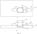
- a PCB assembly 1000 includes a PCB 1100, a first conductor 1200, a first battery 1300, a second battery 1400, a target component 1500, andathird conductor 1800.
- the PCB 1100 includes a groove area 1101.
- the first battery 1300 and the second battery 1400 are disposed on different sides of the groove area 1101.
- the first conductor 1200 is disposed in the groove area 1101.
- the target component 1500 is a component disposed in the groove area 1101.
- the first conductor 1200 is also a bracket that fastens the target component 1500 to the groove area 1101.
- a distance between the second battery 1400 and the groove area 1101 is greater than a preset distance threshold.
- the third conductor 1800 is disposed between the second battery 1400 and the groove area 1101.
- the first battery 1300 and the second battery 1400 are connected by using the third conductor 1800 and the first conductor 1200.
- FIG. 8 is a top view of the PCB assembly 1000
- (b) in FIG. 8 is a side view of the PCB assembly 1000 shown in (a) in FIG. 8 .
- the second conductor 1800 may be used as a power cable that connects the first conductor 1200 and the second battery 1400, and then the first conductor 1200 is connected to the first battery 1300, to implement connection between the first battery 1300 and the second battery 1400.
- the third conductor 1800 may be a metal conductor.
- a metal type of the third conductor 1800 is not limited in this embodiment of this application.
- the third conductor 1800 may be a steel sheet.
- a width of the third conductor 1800 is usually less than a width of a power cable of an inter-PCB cable.
- the PCB assembly includes a PCB, a first conductor, a first battery, a second battery, a target component, and a third conductor.
- the PCB includes a groove area.
- the first battery and the second battery are disposed on different sides of the groove area.
- the first conductor is disposed in the groove area.
- the target component is a component disposed in the groove area.
- the first conductor is also a bracket that fastens the target component to the groove area.
- a distance between the second battery and the groove area is greater than a preset distance threshold.
- the third conductor is disposed between the second battery and the groove area.
- the first battery and the second battery are connected by using the first conductor and the third conductor. That is, when the second battery is disposed at a position away from the groove area, the first battery and the second battery may be connected by using the first conductor and the third conductor, thereby improving flexibility of the disposing position of the second battery.
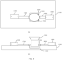
- a PCB assembly 1000 is provided.
- the PCB assembly 1000 includes a PCB 1100, a first conductor 1200, a first battery 1300, a second battery 1400, a target component 1500, a second conductor 1700, and a third conductor 1800.
- the PCB 1100 includes a groove area 1101.
- the first battery 1300 and the second battery 1400 are disposed on different sides of the groove area 1101.
- the first conductor 1200 is disposed in the groove area 1101.
- the target component 1500 is a component disposed in the groove area 1101.
- the first conductor 1200 is also a bracket that fastens the target component 1500 in the groove area 1101.
- a distance between the first battery 1300 and the groove area 1101 is greater than a preset distance threshold.
- the second conductor 1700 is disposed between the first battery 1300 and the groove area 1101, and is configured to connect the first conductor 1200 and the first battery 1300.
- a distance between the second battery 1400 and the groove area 1101 is greater than a preset distance threshold.
- the third conductor 1800 is disposed between the second battery 1400 and the groove area 1101, and is configured to connect the first conductor 1300 and the second battery 1400.
- FIG. 9 is a top view of the PCB assembly 1000
- (b) in FIG. 9 is a side view of the PCB assembly 1000 shown in (a) in FIG. 9 .
- a user needs to place the first battery 1300 and the second battery 1400 in positions far away from the groove area 1101.
- a distance between the first battery 1300 and the groove area 1101 is relatively large, and a distance between the second battery 1400 and the groove area 1101 is relatively large.
- the second conductor 1700 may be used as a power cable that connects the first conductor 1200 and the first battery 1300.
- the distance between the second battery 1400 and the groove area 1101 is also greater than a preset distance threshold.
- the third conductor 1800 is used as a power cable that connects the first conductor 1200 and the second battery 1400. This is equivalent to using the first conductor 1200, the second conductor 1700, and the third conductor 1800 as a power cable that connects the first battery 1300 and the second battery 1400, thereby implementing connection between the first battery 1300 and the second battery 1400.
- Impedance of the power cable between the first battery 1100 and the second battery 1300 must be less than a preset impedance threshold, so that dual-battery power supply can be implemented.
- the impedance of the power cable is closely related to a width thereof. The wider the power cable is, the lower the impedance is. Therefore, a width of each of the first conductor 1200, the second conductor 1700, and the third conductor 1800 that are used to connect the first battery 1100 and the second battery 1300 needs to be greater than a preset width threshold.
- the PCB assembly includes a PCB, a first conductor, a first battery, a second battery, a target component, a second conductor, and a third conductor.
- the PCB includes a groove area, and the first battery and the second battery are disposed on different sides of the groove area.
- the first conductor is disposed in the groove area.
- the target component is a component disposed in the groove area.
- the first conductor is also a bracket that fastens the target component to the groove area.
- a distance between the first battery and the groove area is greater than a preset distance threshold.
- the second conductor is disposed between the first battery and the groove area. The second conductor is configured to connect the first conductor and the first battery.
- a distance between the second battery and the groove area is greater than a preset distance threshold.
- the third conductor is disposed between the second battery and the groove area.
- the third conductor is configured to connect the first conductor and the second battery. That is, when both the first battery and the second battery are far away from the groove area, the first battery and the second battery may be connected by using the first conductor, the second conductor, and the third conductor, thereby improving flexibility of the disposing positions of the first battery and the position of the second battery.
- an electronic device is further provided in this application, where the electronic device includes a printed circuit board PCB assembly, and the PCB assembly includes a PCB, a first conductor, a first battery, and a second battery.
- the PCB includes a groove area.
- the first battery and the second battery are disposed on different sides of the groove area.
- the first conductor is disposed in the groove area, and the first conductor is configured to connect the first battery and the second battery.
- the PCB component further includes a target component, the target component is a component disposed in the groove area, and the first conductor is a bracket that fastens the target component to the groove area.
- the PCB assembly further includes an insulating material, and the insulating material is disposed between the first conductor and the target component.
- the PCB assembly when a distance between the first battery and the groove area is greater than a preset distance threshold, the PCB assembly further includes a second conductor, the second conductor is disposed between the first battery and the groove area, and the second conductor is configured to connect the first conductor and the first battery; and/or when a distance between the second battery and the groove area is greater than the preset distance threshold, the PCB assembly further includes a third conductor, the third conductor is disposed between the second battery and the groove area, and the third conductor is configured to connect the first conductor and the second battery.
- a width of each of the first conductor, the second conductor, and the third conductor is greater than a preset width threshold.
- the first conductor is fastened to the groove area by using a welding method.
- a type of an electronic device is not limited in this embodiment of this application.
- the electronic device may be but is not limited to a mobile phone, a tablet computer, a smart sound box, a smart large screen (also referred to as a smart TV), a wearable device, or the like.
- FIG. 10 is a schematic diagram of a structure of an electronic device 100.
- the electronic device 100 may include a processor 110, an external memory interface 120, an internal memory 121, a universal serial bus (universal serial bus, USB) interface 130, a charging management module 140, a power management module 141, a battery 142, an antenna 1, an antenna 2, a mobile communication module 150, a wireless communication module 160, an audio module 170, a speaker 170A, a receiver 170B, a microphone 170C, a headset jack 170D, a sensor module 180, a key 190, a motor 191, an indicator 192, a camera 193, a display 194, and a subscriber identification module (subscriber identification module, SIM) card interface 195, and the like.
- SIM subscriber identification module
- the sensor module 180 may include a pressure sensor 180A, a gyro sensor 180B, a barometric pressure sensor 180C, a magnetic sensor 180D, an acceleration sensor 180E, a distance sensor 180F, an optical proximity sensor 180G, a fingerprint sensor 180H, a temperature sensor 180J, a touch sensor 180K, an ambient light sensor 180L, a bone conduction sensor 180M, and the like.
- the electronic device 100 may include more or fewer components than those shown in the figure, or combine some components, or split some components, or have different component arrangements.
- the illustrated components may be implemented by using hardware, software or a combination of software and hardware.
- the processor 110 may include one or more processing units.
- the processor 110 may include an application processor (application processor, AP), a modem processor, a graphics processing unit (graphics processing unit, GPU), an image signal processor (image signal processor, ISP), a controller, a memory, a video codec, a digital signal processor (digital signal processor, DSP), a baseband processor, and/or a neural-network processing unit (neural-network processing unit, NPU).
- Different processing units may be independent components, or may be integrated in one or more processors.
- the controller may be a nerve center and a command center of the electronic device 100.
- the controller may generate an operation control signal based on instruction operation code and a timing signal, to complete control of instruction fetch and instruction execution.
- a memory may further be disposed in the processor 110, to store instructions and data.
- the memory in the processor 110 is a cache.
- the memory may store an instruction or data that has just been used or is cyclically used by the processor 110. If the processor 110 needs to use the instructions or the data again, the instructions or the data may be directly invoked from the memory. Therefore, repeated access is avoided, and a waiting time of the processor 110 is reduced, thereby improving system efficiency.
- the interface connection relationship between the modules illustrated in the embodiments of this application is merely an example for description, and does not constitute a limitation on the structure of the electronic device 100.
- the electronic device 100 may alternatively use an interface connection mode that is different from those in the foregoing embodiments, or use a combination of a plurality of interface connection modes.
- the charging management module 140 is configured to receive a charging input from a charger.
- the charger may be a wireless charger or a wired charger.
- the charging management module 140 may receive a charging input of a wired charger by using a USB interface 130.
- the charging management module 140 may receive a wireless charging input by using a wireless charging coil of the electronic device 100.
- the charging management module 140 may further supply power to the electronic device 100 by using the power management module 141.
- the power management module 141 is configured to be connected to the battery 142, the charging management module 140, and the processor 110.
- the power management module 141 receives an input from the battery 142 and/or an input from the charging management module 140, and supplies power to the processor 110, the internal memory 121, an external memory, the display 194, the camera 193, the wireless communication module 160, and the like.
- the power management module 141 may be further configured to monitor a parameter such as a battery capacity, a quantity of battery cycles, and a battery health status (leakage and impedance).
- the power management module 141 may alternatively be disposed in the processor 110.
- the power management module 141 and the charging management module 140 may alternatively be disposed in a same component.
- the electronic device 100 can implement a photographing function by using the ISP, the camera 193, the video codec, the GPU, the display 194, the application processor, and the like.
- the ISP is configured to process data fed back by the camera 193. For example, during photographing, a shutter is opened, light is transmitted to a photosensitive element of the camera by using a lens, an optical signal is converted into an electrical signal, and the electrical signal is transmitted by the photosensitive element of the camera to the ISP for processing and converted into an image visible to a naked eye.
- the ISP may further perform algorithm optimization on noise, brightness, and a skin color of the image.
- the ISP may further optimize parameters such as exposure and a color temperature of a photographing scenario.
- the ISP may be disposed on the camera 193.
- the camera 193 is configured to capture a still image or a video.
- An optical image of an object is generated by using a lens and is projected to a photosensitive element.
- the photosensitive element may be a charge coupled device (charge coupled device, CCD) or a complementary metal-oxide-semiconductor (complementary metal-oxide-semiconductor, CMOS) phototransistor.
- CCD charge coupled device
- CMOS complementary metal-oxide-semiconductor
- the photosensitive element converts an optical signal into an electrical signal, and then transmits the electrical signal to the ISP to convert into a digital image signal.
- the ISP outputs the digital image signal to the DSP for processing.
- the DSP converts the digital image signal into an image signal in a standard format such as RGB or YUV.
- the electronic device 100 may include one or N cameras 193, where N is a positive integer greater than 1.
- the camera 193 may be the foregoing camera module.
- any electronic device mentioned in this embodiment of this application may include more or fewer modules than those in the electronic device 100.
Landscapes
- Engineering & Computer Science (AREA)
- Chemical & Material Sciences (AREA)
- Chemical Kinetics & Catalysis (AREA)
- Electrochemistry (AREA)
- General Chemical & Material Sciences (AREA)
- Microelectronics & Electronic Packaging (AREA)
- Manufacturing & Machinery (AREA)
- Battery Mounting, Suspending (AREA)
Abstract
Description
- This application claims priority to
Chinese Patent Application No. 202111216999. X, filed with the China National Intellectual Property Administration on October 19, 2021 - This application relates to the field of terminal technologies, and in particular, to a printed circuit board PCB assembly and an electronic device.
- To increase a charging speed of terminal devices, dual batteries are increasingly used in the industry as an apparatus for supplying power to terminal devices.
- Supplying power by using dual batteries requires that impedance of a power cable connecting two battery negative electrodes is lower than a preset impedance threshold. As a common low-impedance material, a steel sheet is usually installed on a surface of a printed circuit board (Printed-circuit Board, PCB), and serves as a power cable for connecting two battery negative electrodes. It should be noted that the thicker and wider the conductor, the smaller its impedance. Therefore, a width of a steel sheet that serves as a power cable is usually greater than a preset width threshold. As more and more components are used on the PCB, a steel sheet mounted on a surface occupies a relatively large area on the PCB, and consequently. an area of another component that can be installed on the PCB is reduced.
- Therefore, how to reduce an area proportion of the power cable connecting the two battery negative electrodes on the PCB becomes an urgent problem to be resolved.
- Embodiments of this application provide a printed circuit board PCB assembly and an electronic device, so as to reduce an area proportion of a power cable connecting two battery negative electrodes on a PCB.
- According to a first aspect, a printed circuit board PCB assembly, where the PCB assembly includes a PCB, a first conductor, a first battery, and a second battery; the PCB includes a groove area;
- the first battery and the second battery are disposed on different sides of the groove area; and
- the first conductor is disposed in the groove area, and the first conductor is configured to connect the first battery and the second battery.
- According to the PCB assembly provided in this embodiment of this application, the PCB assembly includes a PCB, a first conductor, a first battery, and a second battery. The PCB includes a groove area. The first battery and the second battery are disposed on different sides of the groove area. The first conductor is disposed in the groove area, and the first conductor is configured to connect the first battery and the second battery. That is, in this embodiment of this application, the first battery and the second battery are connected by using the first conductor in the groove area, thereby preventing a power cable connecting the first battery and the second battery from occupying an area on the PCB, and increasing an area in which other components can be installed on the PCB.
- In an embodiment, the PCB component further includes a target component, the target component is a component disposed in the groove area, and the first conductor is a bracket that fastens the target component to the groove area.
- The PCB assembly provided in this embodiment of this application includes a PCB, a first conductor, a first battery, and a second battery, and a target component. The PCB includes a groove area. The first battery and the second battery are disposed on different sides of the groove area. The first conductor is disposed in the groove area, and the first conductor is a bracket that fastens the target component to the groove area, and is configured to connect the first battery and the second battery. The target component is a component disposed in the groove area. That is, the first conductor that is configured to connect the first battery and the second battery is a reused bracket that fastens the target component to the groove area, thereby further reducing an area occupied by the power cable connecting the first battery and the second battery on the PCB, reducing costs of the PCB assembly, and increasing an area in which other components can be installed on the PCB.
- In an embodiment, the PCB assembly further includes an insulating material, and the insulating material is disposed between the first conductor and the target component.
- In a possible case, when a bottom of the target component is a conductor, disposing the insulating material between the first conductor and the target component can avoid short circuit between the target component and the first battery and the second battery.
- In an embodiment, the target component is a camera module.
- In this embodiment of this application, that the target component is a camera module is equivalent to that the first conductor that is configured to connect the first battery and the second battery reuses the bracket that fastens the target component to the groove area, thereby further reducing an area occupied by the power cable connecting the first battery and the second battery on the PCB, reducing costs of the PCB assembly, and increasing an area in which other components can be installed on the PCB.
- In an embodiment, when a distance between the first battery and the groove area is greater than a preset distance threshold, the PCB assembly further includes a second conductor, the second conductor is disposed between the first battery and the groove area, and the second conductor is configured to connect the first conductor and the first battery; and/or when a distance between the second battery and the groove area is greater than the preset distance threshold, the PCB assembly further includes a third conductor, the third conductor is disposed between the second battery and the groove area, and the third conductor is configured to connect the first conductor and the second battery.
- In this embodiment of this application, the PCB assembly includes a PCB, a first conductor, a first battery, a second battery, a target component, and a second conductor. The PCB includes a groove area. The first battery and the second battery are disposed on different sides of the groove area. The first conductor is disposed in the groove area. The target component is a component disposed in the groove area. The first conductor is also a bracket that fastens the target component to the groove area. A distance between the first battery and the groove area is greater than a preset distance threshold. The second conductor is disposed between the first battery and the groove area. The second conductor is connected to the first battery and the second battery by using the first conductor and the second conductor. That is, the first battery may be disposed in a position far away from the groove area, and does not need to be disposed close to the groove area. When the first battery is disposed at the position away from the groove area, the first battery and the second battery may be connected by using the first conductor and the second conductor, thereby improving flexibility of the disposing position of the first battery.
- In an embodiment, a width of each of the first conductor, the second conductor, and the third conductor is greater than a preset width threshold.
- In an embodiment, the first conductor is fastened to the groove area by using a welding method.
- In this embodiment of this application, the first conductor is fastened to the groove area by using a welding method. Only a relatively small pad needs to be disposed on the PCB, so that the first conductor can be fastened to the groove area. This further reduces an area occupied by the power cable of the first battery and the second battery on the PCB, and increases an area in which other components can be installed on the PCB.
- According to a second aspect, an electronic device is provided, where the electronic device includes a printed circuit board PCB assembly, and the PCB assembly includes a PCB, a first conductor, a first battery, and a second battery; the PCB includes a groove area; the first battery and the second battery are disposed on different sides of the groove area; and the first conductor is disposed in a groove area, and the first conductor is configured to connect the first battery and the second battery.
- In an embodiment, the PCB component further includes a target component, the target component is a component disposed in the groove area, and the first conductor is a bracket that fastens the target component to the groove area.
- In an embodiment, the PCB assembly further includes an insulating material, and the insulating material is disposed between the first conductor and the target component.
- In an embodiment, when a distance between the first battery and the groove area is greater than a preset distance threshold, the PCB assembly further includes a second conductor, the second conductor is disposed between the first battery and the groove area, and the second conductor is configured to connect the first conductor and the first battery; and/or when a distance between the second battery and the groove area is greater than the preset distance threshold, the PCB assembly further includes a third conductor, the third conductor is disposed between the second battery and the groove area, and the third conductor is configured to connect the first conductor and the second battery.
- In an embodiment, a width of each of the first conductor, the second conductor, and the third conductor is greater than a preset width threshold.
- In an embodiment, the first conductor is fastened to the groove area by using a welding method.
-
-
FIG. 1 is a schematic diagram of a dual-power connection; -
FIG. 2 is a schematic diagram of an application scenario of a PCB assembly according to an embodiment of this application; -
FIG. 3 is a schematic diagram of a structure of a PCB assembly according to an embodiment of this application; -
FIG. 4 is a schematic diagram of a battery position of a PCB assembly according to an embodiment of this application; -
FIG. 5 is a schematic diagram of a structure a PCB assembly according to another embodiment of this application; -
FIG. 6 is a schematic diagram of a structure of a first conductor, an insulating material, and a target component according to an embodiment of this application; -
FIG. 7 is a schematic diagram of a structure a PCB assembly according to another embodiment of this application; -
FIG. 8 is a schematic diagram of a structure a PCB assembly according to another embodiment of this application; -
FIG. 9 is a schematic diagram of a structure a PCB assembly according to another embodiment of this application; and -
FIG. 10 is a schematic diagram of an electronic device according to an embodiment of this application. - Technical solutions in the embodiments of this application are described below with reference to the accompanying drawings in the embodiments of this application. In descriptions of embodiments of this application, unless otherwise specified, "/" means "or", for example, A/B may mean "A or B"; "and/or" used herein is only used to describe an association relationship between associated obj ects, and indicates that three relationships may exist. For example, "A and/or B" may indicate the following: Only A exists, both A and B exist, and only B exists. In addition, in the descriptions of embodiments of this application, "a plurality of means two or more than two.
- In the following, the terms "first", "second", and "third" are used for descriptive purposes only, and cannot be construed as indicating or implying relative importance or implicitly indicating the quantity of technical features indicated. Therefore, the features defined with "first", "second" and "third" may explicitly or implicitly include one or more of the features.
- A PCB assembly provided in embodiments of this application may be applied to an electronic device. Optionally, the electronic device may be a laptop computer, a tablet computer, a palmtop computer, a vehicle-mounted terminal, a point of sales terminal, a wearable device, a mobile phone, or the like.
- Currently, an electronic device using dual-battery power supply is used, and negative electrodes of the two batteries are connected by using a power cable. For example, as shown in
FIG. 1 , a power cable connecting two battery negative electrodes may be a steel sheet, and the steel sheet may be attached to a surface of the PCB by using a surface mounted technology (Surface Mounted Technology, SMT). The steel sheet is grounded by using a precision detection resistor, and the precision detection resistor may be configured to detect a current value on the steel sheet. To ensure good performance of the dual-battery power supply, it is usually required that impedance of the power cable connecting two battery negative electrodes is lower than a preset impedance threshold (for example, 2 mohms). The wider the conductor is, the lower the impedance is. Therefore, a width of the steel sheet is relatively large. - To increase a component-installable area on a PCB, the PCB assembly provided in this embodiment of this application includes a PCB, a first battery, a second battery, and a first conductor. There is a groove area on the PCB, and the first conductor is a conductor disposed in the groove area, and may be configured to support a component disposed in the groove area. The first battery and the second battery are disposed on different sides of the groove area. For example, as shown in (a) in
FIG. 2 , the first battery is disposed on a left side of the groove area, and the second battery is disposed on a right side of the groove area. As shown in (b) inFIG. 2 , in this application, the first conductor in the groove area is reused as a power cable that connects the first battery and the second battery, so that the power cable that connects the first battery and the second battery does not need to occupy an additional area of the PCB, thereby increasing an of an component-installable area on the PCB. - The following describes in detail the PCB assembly provided in embodiments of this application with reference to
FIG. 3 to FIG. 10 . - As shown in
FIG. 3 , an embodiment of this application provides aPCB assembly 1000, and thePCB assembly 1000 includes aPCB 1100, afirst conductor 1200, afirst battery 1300, and asecond battery 1400. ThePCB 1100 includes agroove area 1101. Thefirst battery 1300 and thesecond battery 1400 are disposed on different sides of thegroove area 1101. Thefirst conductor 1200 is disposed in agroove area 1101, and thefirst conductor 1200 is configured to connect thefirst battery 1300 and thesecond battery 1400. - It should be noted that (a) in
FIG. 3 is a top view of thePCB assembly 1000 according to an embodiment of this application, and (b) inFIG. 3 is a side view of thePCB assembly 1000 shown in (a) inFIG. 3 . - It should be understood that the
groove area 1101 may be disposed in any area on thePCB 1100. A position of thegroove area 1101 on thePCB 1100 is not limited in this embodiment of this application. Thefirst battery 1300 and thesecond battery 1400 are disposed on different sides of thegroove area 1101. - For example, as shown in (a) in
FIG. 4 , thefirst battery 1300 may be disposed on a left side of thegroove area 1101, and thesecond battery 1400 is disposed on a right side of thegroove area 1101. Alternatively, as shown in (b) inFIG. 4 , thefirst battery 1300 may be disposed on the left side of thegroove area 1101, and thesecond battery 1400 is disposed on a top of thegroove area 1101. Alternatively, as shown in (c) inFIG. 4 , thefirst battery 1300 may be disposed on the left side of thegroove area 1101, and thesecond battery 1400 is disposed under thegroove area 1101. That is, thefirst battery 1300 and thesecond battery 1400 may be flexibly disposed on different sides of thegroove area 1101 based on a requirement of the user. - The following uses an example in which the
first battery 1300 is disposed on the left side of thegroove area 1101, and thesecond battery 1400 is disposed on the right side of thegroove area 1101 to describe how to connect thefirst battery 1300 and thesecond battery 1400 by using thefirst conductor 1200. - The
first conductor 1200 is a metal conductor disposed on thegroove area 1101. A metal type of thefirst conductor 1200 is not limited in embodiments of this application. In a possible case, thefirst conductor 1200 may be a bracket configured to support a component installed on thePCB 1100. When thefirst conductor 1200 is bracket that supports a component, thefirst conductor 1200 may be a steel sheet. Because a resistance coefficient of a steel material is relatively low, a width of thefirst conductor 1200 may be less than a width of a power cable of an inter-PCB cable. - For example, as shown in (a) in
FIG. 3 and (b) inFIG. 3 , when thefirst battery 1300 is disposed on the left side of thegroove area 1101 and thesecond battery 1400 is disposed on the right side of thegroove area 1101, thefirst conductor 1200 may be used as a power cable that connects a negative electrode of thefirst battery 1300 and a negative electrode of thesecond battery 1400, so that the negative electrode of thefirst battery 1300 and the negative electrode of thesecond battery 1400 are conductive, thereby implementing dual-battery power supply of the electronic device. - According to the PCB assembly provided in this embodiment of this application, the PCB assembly includes a PCB, a first conductor, a first battery, and a second battery. The PCB includes a groove area. The first battery and the second battery are disposed on different sides of the groove area. The first conductor is disposed in the groove area, and the first conductor is configured to connect the first battery and the second battery. That is, in this embodiment of this application, the first battery and the second battery are connected by using the first conductor in the groove area, thereby preventing a power cable connecting the first battery and the second battery from occupying an area on the PCB, and increasing an area in which other components can be installed on the PCB.
- In an embodiment, as shown in
FIG. 5 , aPCB assembly 1000 is provided. ThePCB assembly 1000 includes aPCB 1100, afirst conductor 1200, afirst battery 1300, asecond battery 1400, and atarget component 1500. ThePCB 1100 includes agroove area 1101. Thefirst battery 1300 and thesecond battery 1400 are disposed on different sides of thegroove area 1101. Thefirst conductor 1200 is disposed in thegroove area 1101. Thefirst conductor 1200 is configured to connect thefirst battery 1300 and thesecond battery 1400. Thetarget component 1500 is a component disposed in thegroove area 1101. Thefirst conductor 1200 is also a bracket that fastens thetarget component 1500 to thegroove area 1101. - It should be noted that (a) in
FIG. 5 is a top view of thePCB assembly 1000, and (b) inFIG. 5 is a side view of thePCB assembly 1000 shown in (a) inFIG. 5 . - Generally, the
target component 1500 is a component with a relatively large size. When thetarget component 1500 is installed on thePCB 1100, a groove needs to be dug on thePCB 1100 to obtain thegroove area 1101, and then thetarget component 1500 is installed in the groove area. A type of thetarget component 1500 is not limited in this embodiment of this application. - Optionally, the
target component 1500 may be a camera module. - The
first conductor 1200 is a bracket that fastens thetarget component 1500 to thegroove area 1101. It should be noted that a connection apparatus for fastening thetarget component 1500 to thefirst conductor 1200 is disposed on thefirst conductor 1200. Then, thefirst conductor 1200 may be fastened to thegroove area 1101, so that thefirst conductor 1200 can be fastened to thegroove area 1101, and thetarget component 1500 can be fastened to the groove area. - When the
target component 1500 is a camera module, because the camera module is usually large, a width of thefirst conductor 1200 used to fasten the camera module is also usually large. For example, the width of thefirst conductor 1200 may be the same as the width of the camera module. For example, when the width of the camera module is 7.8 mm, the width of thefirst conductor 1200 may be set to 7.8 mm, and a thickness may be set to 0.2 mm. When the width of thefirst conductor 1200 is the same as the width of the camera module, thefirst conductor 1200 can better support the camera module. - In a possible case, the width of the
first conductor 1200 may be less than the width of thetarget component 1500. It should be noted that impedance of the power cable between thefirst battery 1300 and thesecond battery 1400 must be less than a preset impedance threshold, so that dual-battery power supply can be implemented. The impedance of the power cable is closely related to a width thereof. The wider the power cable is, the lower the impedance is. Therefore, the width of thefirst conductor 1200 used to connect thefirst battery 1300 and thesecond battery 1400 needs to be greater than a preset width threshold. The preset width threshold may be obtained through calculation according to an impedance calculation formula of the conductor. For example, according to the impedance calculation formula of the conductor, a minimum width of thefirst conductor 1200 may be set to 3 mm, and a thickness may be set to 0.2 mm. When the width of the first conductor is less than the width of thetarget component 1500, a total area of thefirst conductor 1500 is relatively small, and costs of thefirst conductor 1500 may be reduced. - In conclusion, the width of the
first conductor 1200 may be the same as or different from the width of thetarget component 1500, which is not limited in this embodiment of this application. - For example, a clamping groove may be disposed on the
first conductor 1200, and the clamping groove is used to fasten thetarget component 1500 to thefirst conductor 1200. Alternatively, an adhesive material may be disposed on thefirst conductor 1200, and thetarget component 1500 is bonded to thefirst conductor 1200. This is not limited in this embodiment of this application. - For example, the
first conductor 1200 may be fastened to thegroove area 1101 by using a welding method. For example, a flange for welding is disposed on thefirst conductor 1200, and a pad is disposed on an area adjacent to thegroove area 1101 on the PCB 1100 (an area of the pad is usually relatively small). By welding the flange on thefirst conductor 1200 to the pad disposed on the adjacent area, thefirst conductor 1200 is fastened to thegroove area 1101. - In this embodiment of this application, the first conductor is fastened to the groove area by using a welding method. Only a relatively small pad needs to be disposed on the PCB, so that the first conductor can be fastened to the groove area. This further reduces an area occupied by the power cable of the first battery and the second battery on the PCB, and increases an area in which other components can be installed on the PCB.
- To avoid short circuit between the
target component 1500 and thefirst battery 1300 and thesecond battery 1400, optionally, as shown inFIG. 6 , an insulatingmaterial 1600 may be disposed between thefirst conductor 1200 and thetarget component 1500. - The insulating
material 1600 is usually a material with excellent electrical insulation, which can still maintain electrical insulation well at high frequencies. For example, the insulatingmaterial 1600 may be Polyethylene terephthalate (Polyethylene terephthalate, PET). - The PCB assembly provided in this embodiment of this application includes a PCB, a first conductor, a first battery, and a second battery, and a target component. The PCB includes a groove area. The first battery and the second battery are disposed on different sides of the groove area. The first conductor is disposed in the groove area, and the first conductor is a bracket that fastens the target component to the groove area, and is configured to connect the first battery and the second battery. The target component is a component disposed in the groove area. That is, the first conductor that is configured to connect the first battery and the second battery is a reused bracket that fastens the target component to the groove area, thereby further reducing an area occupied by the power cable connecting the first battery and the second battery on the PCB, reducing costs of the PCB assembly, and increasing an area in which other components can be installed on the PCB.
- In an example, as shown in
FIG. 7 , aPCB assembly 1000 is provided. ThePCB assembly 1000 includes aPCB 1100, afirst conductor 1200, afirst battery 1300, asecond battery 1400, atarget component 1500, and asecond conductor 1700. ThePCB 1100 includes agroove area 1101. Thefirst battery 1300 and thesecond battery 1400 are disposed on different sides of thegroove area 1101. Thefirst conductor 1200 is disposed in thegroove area 1101. Thetarget component 1500 is a component disposed in thegroove area 1101. Thefirst conductor 1200 is also a bracket that fastens thetarget component 1500 to thegroove area 1101. A distance between thefirst battery 1300 and thegroove area 1101 is greater than a preset distance threshold. Thesecond conductor 1700 is disposed between thefirst battery 1300 and thegroove area 1101. Thefirst battery 1300 and thesecond battery 1400 are connected by using thesecond conductor 1700 and thefirst conductor 1200. - It should be noted that (a) in
FIG. 7 is a top view of thePCB assembly 1000, and (b) inFIG. 7 is a side view of thePCB assembly 1000 shown in (a) inFIG. 7 . - In a possible case, a user needs to place the
first battery 1300 in a position away from thegroove area 1101. In this case, the distance between thefirst battery 1300 and thegroove area 1101 is large. When the distance between thefirst battery 1300 and thegroove area 1101 is greater than the preset distance threshold, thesecond conductor 1700 may be used as a power cable that connects thefirst conductor 1200 and thefirst battery 1300, and then thefirst conductor 1200 is connected to thesecond battery 1400, to implement connection between thefirst battery 1300 and thesecond battery 1400. - It should be noted that the
second conductor 1700 may be a metal conductor, and a metal type of thesecond conductor 1200 is not limited in this embodiment of this application. In an example, thesecond conductor 1700 may be a steel sheet. When thesecond conductor 1700 is a steel sheet, because a resistance coefficient of the steel material is relatively low, a width of thesecond conductor 1700 is usually less than a width of a power cable of an inter-PCB cable. - In this embodiment of this application, the PCB assembly includes a PCB, a first conductor, a first battery, a second battery, a target component, and a second conductor. The PCB includes a groove area. The first battery and the second battery are disposed on different sides of the groove area. The first conductor is disposed in the groove area. The target component is a component disposed in the groove area. The first conductor is also a bracket that fastens the target component to the groove area. A distance between the first battery and the groove area is greater than a preset distance threshold. The second conductor is disposed between the first battery and the groove area. The second conductor is connected to the first battery and the second battery by using the first conductor and the second conductor. That is, the first battery may be disposed in a position far away from the groove area, and does not need to be disposed close to the groove area. When the first battery is disposed at the position away from the groove area, the first battery and the second battery may be connected by using the first conductor and the second conductor, thereby improving flexibility of the disposing position of the first battery.
- In an example, as shown in
FIG. 8 , aPCB assembly 1000 is provided. ThePCB assembly 1000 includes aPCB 1100, afirst conductor 1200, afirst battery 1300, asecond battery 1400, atarget component 1500,andathird conductor 1800. ThePCB 1100 includes agroove area 1101. Thefirst battery 1300 and thesecond battery 1400 are disposed on different sides of thegroove area 1101. Thefirst conductor 1200 is disposed in thegroove area 1101. Thetarget component 1500 is a component disposed in thegroove area 1101. Thefirst conductor 1200 is also a bracket that fastens thetarget component 1500 to thegroove area 1101. A distance between thesecond battery 1400 and thegroove area 1101 is greater than a preset distance threshold. Thethird conductor 1800 is disposed between thesecond battery 1400 and thegroove area 1101. Thefirst battery 1300 and thesecond battery 1400 are connected by using thethird conductor 1800 and thefirst conductor 1200. - It should be noted that (a) in
FIG. 8 is a top view of thePCB assembly 1000, and (b) inFIG. 8 is a side view of thePCB assembly 1000 shown in (a) inFIG. 8 . - In a possible case, a user needs to place the
second battery 1400 in a position away from thegroove area 1101. In this case, the distance between thesecond battery 1400 and thegroove area 1101 is large. When the distance between thesecond battery 1400 and thegroove area 1101 is greater than the preset distance threshold, thesecond conductor 1800 may be used as a power cable that connects thefirst conductor 1200 and thesecond battery 1400, and then thefirst conductor 1200 is connected to thefirst battery 1300, to implement connection between thefirst battery 1300 and thesecond battery 1400. - The
third conductor 1800 may be a metal conductor. A metal type of thethird conductor 1800 is not limited in this embodiment of this application. In an example, thethird conductor 1800 may be a steel sheet. When thethird conductor 1800 is a steel sheet, because a resistance coefficient of the steel material is relatively low, a width of thethird conductor 1800 is usually less than a width of a power cable of an inter-PCB cable. - In this embodiment of this application, the PCB assembly includes a PCB, a first conductor, a first battery, a second battery, a target component, and a third conductor. The PCB includes a groove area. The first battery and the second battery are disposed on different sides of the groove area. The first conductor is disposed in the groove area. The target component is a component disposed in the groove area. The first conductor is also a bracket that fastens the target component to the groove area. A distance between the second battery and the groove area is greater than a preset distance threshold. The third conductor is disposed between the second battery and the groove area. The first battery and the second battery are connected by using the first conductor and the third conductor. That is, when the second battery is disposed at a position away from the groove area, the first battery and the second battery may be connected by using the first conductor and the third conductor, thereby improving flexibility of the disposing position of the second battery.
- In an example, as shown in
FIG. 9 , aPCB assembly 1000 is provided. ThePCB assembly 1000 includes aPCB 1100, afirst conductor 1200, afirst battery 1300, asecond battery 1400, atarget component 1500, asecond conductor 1700, and athird conductor 1800. ThePCB 1100 includes agroove area 1101. Thefirst battery 1300 and thesecond battery 1400 are disposed on different sides of thegroove area 1101. Thefirst conductor 1200 is disposed in thegroove area 1101. Thetarget component 1500 is a component disposed in thegroove area 1101. Thefirst conductor 1200 is also a bracket that fastens thetarget component 1500 in thegroove area 1101. A distance between thefirst battery 1300 and thegroove area 1101 is greater than a preset distance threshold. Thesecond conductor 1700 is disposed between thefirst battery 1300 and thegroove area 1101, and is configured to connect thefirst conductor 1200 and thefirst battery 1300. A distance between thesecond battery 1400 and thegroove area 1101 is greater than a preset distance threshold. Thethird conductor 1800 is disposed between thesecond battery 1400 and thegroove area 1101, and is configured to connect thefirst conductor 1300 and thesecond battery 1400. - It should be noted that (a) in
FIG. 9 is a top view of thePCB assembly 1000, and (b) inFIG. 9 is a side view of thePCB assembly 1000 shown in (a) inFIG. 9 . - In a possible case, a user needs to place the
first battery 1300 and thesecond battery 1400 in positions far away from thegroove area 1101. In this case, a distance between thefirst battery 1300 and thegroove area 1101 is relatively large, and a distance between thesecond battery 1400 and thegroove area 1101 is relatively large. When the distance between thefirst battery 1300 and thegroove area 1101 is greater than a preset distance threshold, thesecond conductor 1700 may be used as a power cable that connects thefirst conductor 1200 and thefirst battery 1300. In addition, the distance between thesecond battery 1400 and thegroove area 1101 is also greater than a preset distance threshold. Thethird conductor 1800 is used as a power cable that connects thefirst conductor 1200 and thesecond battery 1400. This is equivalent to using thefirst conductor 1200, thesecond conductor 1700, and thethird conductor 1800 as a power cable that connects thefirst battery 1300 and thesecond battery 1400, thereby implementing connection between thefirst battery 1300 and thesecond battery 1400. - Impedance of the power cable between the
first battery 1100 and thesecond battery 1300 must be less than a preset impedance threshold, so that dual-battery power supply can be implemented. The impedance of the power cable is closely related to a width thereof. The wider the power cable is, the lower the impedance is. Therefore, a width of each of thefirst conductor 1200, thesecond conductor 1700, and thethird conductor 1800 that are used to connect thefirst battery 1100 and thesecond battery 1300 needs to be greater than a preset width threshold. - In this embodiment of this application, the PCB assembly includes a PCB, a first conductor, a first battery, a second battery, a target component, a second conductor, and a third conductor. The PCB includes a groove area, and the first battery and the second battery are disposed on different sides of the groove area. The first conductor is disposed in the groove area. The target component is a component disposed in the groove area. The first conductor is also a bracket that fastens the target component to the groove area. A distance between the first battery and the groove area is greater than a preset distance threshold. The second conductor is disposed between the first battery and the groove area. The second conductor is configured to connect the first conductor and the first battery. A distance between the second battery and the groove area is greater than a preset distance threshold. The third conductor is disposed between the second battery and the groove area. The third conductor is configured to connect the first conductor and the second battery. That is, when both the first battery and the second battery are far away from the groove area, the first battery and the second battery may be connected by using the first conductor, the second conductor, and the third conductor, thereby improving flexibility of the disposing positions of the first battery and the position of the second battery.
- In a possible case, an electronic device is further provided in this application, where the electronic device includes a printed circuit board PCB assembly, and the PCB assembly includes a PCB, a first conductor, a first battery, and a second battery. The PCB includes a groove area. The first battery and the second battery are disposed on different sides of the groove area. The first conductor is disposed in the groove area, and the first conductor is configured to connect the first battery and the second battery.
- In an embodiment, the PCB component further includes a target component, the target component is a component disposed in the groove area, and the first conductor is a bracket that fastens the target component to the groove area.
- In an embodiment, the PCB assembly further includes an insulating material, and the insulating material is disposed between the first conductor and the target component.
- In an embodiment, when a distance between the first battery and the groove area is greater than a preset distance threshold, the PCB assembly further includes a second conductor, the second conductor is disposed between the first battery and the groove area, and the second conductor is configured to connect the first conductor and the first battery; and/or when a distance between the second battery and the groove area is greater than the preset distance threshold, the PCB assembly further includes a third conductor, the third conductor is disposed between the second battery and the groove area, and the third conductor is configured to connect the first conductor and the second battery.
- In an embodiment, a width of each of the first conductor, the second conductor, and the third conductor is greater than a preset width threshold.
- In an embodiment, the first conductor is fastened to the groove area by using a welding method.
- An implementation method and technical effects of the electronic device provided in this embodiment of this application are similar to those of the foregoing PCB assembly, and details are not described herein again.
- A type of an electronic device is not limited in this embodiment of this application. For example, the electronic device may be but is not limited to a mobile phone, a tablet computer, a smart sound box, a smart large screen (also referred to as a smart TV), a wearable device, or the like.
- For example,
FIG. 10 is a schematic diagram of a structure of anelectronic device 100. Theelectronic device 100 may include aprocessor 110, anexternal memory interface 120, an internal memory 121, a universal serial bus (universal serial bus, USB) interface 130, acharging management module 140, apower management module 141, abattery 142, anantenna 1, anantenna 2, amobile communication module 150, awireless communication module 160, anaudio module 170, aspeaker 170A, areceiver 170B, amicrophone 170C, aheadset jack 170D, asensor module 180, a key 190, amotor 191, anindicator 192, acamera 193, adisplay 194, and a subscriber identification module (subscriber identification module, SIM) card interface 195, and the like. Thesensor module 180 may include apressure sensor 180A, agyro sensor 180B, a barometric pressure sensor 180C, amagnetic sensor 180D, anacceleration sensor 180E, adistance sensor 180F, an optical proximity sensor 180G, afingerprint sensor 180H, atemperature sensor 180J, atouch sensor 180K, an ambient light sensor 180L, abone conduction sensor 180M, and the like. - It may be understood that a structure shown in this embodiment of this application does not constitute a specific limitation on the
electronic device 100. In some other embodiments of this application, theelectronic device 100 may include more or fewer components than those shown in the figure, or combine some components, or split some components, or have different component arrangements. The illustrated components may be implemented by using hardware, software or a combination of software and hardware. - The
processor 110 may include one or more processing units. For example, theprocessor 110 may include an application processor (application processor, AP), a modem processor, a graphics processing unit (graphics processing unit, GPU), an image signal processor (image signal processor, ISP), a controller, a memory, a video codec, a digital signal processor (digital signal processor, DSP), a baseband processor, and/or a neural-network processing unit (neural-network processing unit, NPU). Different processing units may be independent components, or may be integrated in one or more processors. - The controller may be a nerve center and a command center of the
electronic device 100. The controller may generate an operation control signal based on instruction operation code and a timing signal, to complete control of instruction fetch and instruction execution. - A memory may further be disposed in the
processor 110, to store instructions and data. In some embodiments, the memory in theprocessor 110 is a cache. The memory may store an instruction or data that has just been used or is cyclically used by theprocessor 110. If theprocessor 110 needs to use the instructions or the data again, the instructions or the data may be directly invoked from the memory. Therefore, repeated access is avoided, and a waiting time of theprocessor 110 is reduced, thereby improving system efficiency. - It can be understood that the interface connection relationship between the modules illustrated in the embodiments of this application is merely an example for description, and does not constitute a limitation on the structure of the
electronic device 100. In some other embodiments of this application, theelectronic device 100 may alternatively use an interface connection mode that is different from those in the foregoing embodiments, or use a combination of a plurality of interface connection modes. - The
charging management module 140 is configured to receive a charging input from a charger. The charger may be a wireless charger or a wired charger. In some embodiments of wired charging, thecharging management module 140 may receive a charging input of a wired charger by using a USB interface 130. In some embodiments of wireless charging, thecharging management module 140 may receive a wireless charging input by using a wireless charging coil of theelectronic device 100. When charging thebattery 142, thecharging management module 140 may further supply power to theelectronic device 100 by using thepower management module 141. - The
power management module 141 is configured to be connected to thebattery 142, thecharging management module 140, and theprocessor 110. Thepower management module 141 receives an input from thebattery 142 and/or an input from thecharging management module 140, and supplies power to theprocessor 110, the internal memory 121, an external memory, thedisplay 194, thecamera 193, thewireless communication module 160, and the like. Thepower management module 141 may be further configured to monitor a parameter such as a battery capacity, a quantity of battery cycles, and a battery health status (leakage and impedance). In some other embodiments, thepower management module 141 may alternatively be disposed in theprocessor 110. In some other embodiments, thepower management module 141 and thecharging management module 140 may alternatively be disposed in a same component. - The
electronic device 100 can implement a photographing function by using the ISP, thecamera 193, the video codec, the GPU, thedisplay 194, the application processor, and the like. - The ISP is configured to process data fed back by the
camera 193. For example, during photographing, a shutter is opened, light is transmitted to a photosensitive element of the camera by using a lens, an optical signal is converted into an electrical signal, and the electrical signal is transmitted by the photosensitive element of the camera to the ISP for processing and converted into an image visible to a naked eye. The ISP may further perform algorithm optimization on noise, brightness, and a skin color of the image. The ISP may further optimize parameters such as exposure and a color temperature of a photographing scenario. In some embodiments, the ISP may be disposed on thecamera 193. - The
camera 193 is configured to capture a still image or a video. An optical image of an object is generated by using a lens and is projected to a photosensitive element. The photosensitive element may be a charge coupled device (charge coupled device, CCD) or a complementary metal-oxide-semiconductor (complementary metal-oxide-semiconductor, CMOS) phototransistor. The photosensitive element converts an optical signal into an electrical signal, and then transmits the electrical signal to the ISP to convert into a digital image signal. The ISP outputs the digital image signal to the DSP for processing. The DSP converts the digital image signal into an image signal in a standard format such as RGB or YUV. In some embodiments, theelectronic device 100 may include one orN cameras 193, where N is a positive integer greater than 1. In some embodiments, thecamera 193 may be the foregoing camera module. - It should be noted that any electronic device mentioned in this embodiment of this application may include more or fewer modules than those in the
electronic device 100. - In the foregoing embodiments, descriptions of the embodiments have respective focuses. For a part that is not detailed or described in an embodiment, refer to related descriptions in other embodiments. It should be understood that sequence numbers of the foregoing steps do not mean execution sequences in the embodiments. The execution sequences of the processes should be determined based on functions and internal logic of the processes, and should not be construed as any limitation on the implementation processes of the embodiments of this application. In addition, as used herein, the terms such as "first", "second", and "third" are used only for the purpose of description, and should not be understood as indicating or implying relative importance. Referring to "one embodiment" or "some embodiments" or the like described in the specification of this application means that one or more embodiments of this application include a specific feature, structure, or characteristic described with reference to the embodiment. Therefore, the statements "in one embodiment", "in some embodiments", "in some other embodiments", and the like appearing at different positions in this specification do not mean that these embodiments are all necessarily referred to, but mean "one or more but not all embodiments", unless otherwise specifically emphasized in other ways.
- Finally, it should be noted that the foregoing descriptions are merely specific implementations of this application, but are not intended to limit the protection scope of this application. Any variation or replacement within the technical scope disclosed in this application shall fall within the protection scope of this application. Therefore, the protection scope of this application shall be subject to the protection scope of the claims.
Claims (12)
- A printed circuit board PCB assembly, wherein the PCB assembly comprises a PCB, a first conductor, a first battery, and a second battery; the PCB comprises a groove area;the first battery and the second battery are disposed on different sides of the groove area; andthe first conductor is disposed in the groove area, and the first conductor is configured to connect the first battery and the second battery.
- The PCB assembly according to claim 1, wherein the PCB assembly further comprises a target component, the target component is a component disposed in the groove area, and the first conductor is a bracket that fastens the target component to the groove area.
- The PCB assembly according to claim 2, wherein the PCB assembly further comprises an insulating material, and the insulating material is disposed between the first conductor and the target component.
- The PCB assembly according to any one of claims 1 to 3, wherein when a distance between the first battery and the groove area is greater than a preset distance threshold, the PCB assembly further comprises a second conductor, the second conductor is disposed between the first battery and the groove area, and the second conductor is configured to connect the first conductor and the first battery; and/or
when a distance between the second battery and the groove area is greater than the preset distance threshold, the PCB assembly further comprises a third conductor, the third conductor is disposed between the second battery and the groove area, and the third conductor is configured to connect the first conductor and the second battery. - The PCB assembly according to claim 4, wherein a width of each of the first conductor, the second conductor, and the third conductor is greater than a preset width threshold.
- The PCB assembly according to any one of claims 1 to 5, wherein the first conductor is fastened to the groove area by using a welding method.
- An electronic device, wherein the electronic device comprises a printed circuit board PCB assembly, and the PCB assembly comprises a PCB, a first conductor, a first battery, and a second battery; the PCB comprises a groove area;the first battery and the second battery are disposed on different sides of the groove area; andthe first conductor is disposed in the groove area, and the first conductor is configured to connect the first battery and the second battery.
- The electronic device according to claim 7, wherein the PCB assembly further comprises a target component, the target component is a component disposed in the groove area, and the first conductor is a bracket that fastens the target component to the groove area.
- The electronic device according to claim 8, wherein the PCB assembly further comprises an insulating material, and the insulating material is disposed between the first conductor and the target component.
- The electronic device according to any one of claims 7 to 9, wherein when a distance between the first battery and the groove area is greater than a preset distance threshold, the PCB assembly further comprises a second conductor, the second conductor is disposed between the first battery and the groove area, and the second conductor is configured to connect the first conductor and the first battery; and/or
when a distance between the second battery and the groove area is greater than the preset distance threshold, the PCB assembly further comprises a third conductor, the third conductor is disposed between the second battery and the groove area, and the third conductor is configured to connect the first conductor and the second battery. - The electronic device according to claim 10, wherein a width of each of the first conductor, the second conductor, and the third conductor is greater than a preset width threshold.
- The electronic device according to any one of claims 7 to 11, wherein the first conductor is fastened to the groove area by using a welding method.
Applications Claiming Priority (2)
| Application Number | Priority Date | Filing Date | Title |
|---|---|---|---|
| CN202111216999.XA CN115000638B (en) | 2021-10-19 | 2021-10-19 | Printed circuit board PCB assembly and electronic equipment |
| PCT/CN2022/115914 WO2023065836A1 (en) | 2021-10-19 | 2022-08-30 | Printed circuit board (pcb) assembly and electronic device |
Publications (3)
| Publication Number | Publication Date |
|---|---|
| EP4195398A1 true EP4195398A1 (en) | 2023-06-14 |
| EP4195398A4 EP4195398A4 (en) | 2024-08-07 |
| EP4195398B1 EP4195398B1 (en) | 2025-09-17 |
Family
ID=83018271
Family Applications (1)
| Application Number | Title | Priority Date | Filing Date |
|---|---|---|---|
| EP22847104.1A Active EP4195398B1 (en) | 2021-10-19 | 2022-08-30 | Printed circuit board (pcb) assembly and electronic device |
Country Status (4)
| Country | Link |
|---|---|
| US (1) | US12127347B2 (en) |
| EP (1) | EP4195398B1 (en) |
| CN (2) | CN115000638B (en) |
| WO (1) | WO2023065836A1 (en) |
Family Cites Families (16)
| Publication number | Priority date | Publication date | Assignee | Title |
|---|---|---|---|---|
| JPS60125768U (en) * | 1984-02-02 | 1985-08-24 | キヤノン株式会社 | electrical circuit board |
| JPH0722005A (en) * | 1993-07-06 | 1995-01-24 | Yuasa Corp | Battery layout method for printed circuit board |
| JP3625778B2 (en) | 2001-03-30 | 2005-03-02 | 三洋電機株式会社 | Printed circuit board for mounting coin-type electrical elements |
| CN1787542A (en) * | 2004-12-06 | 2006-06-14 | 明基电通股份有限公司 | Electronic device and battery replacement method thereof |
| CN201690250U (en) | 2010-05-21 | 2010-12-29 | 希姆通信息技术(上海)有限公司 | Double-cell electric-supplying device |
| TWM417912U (en) * | 2011-03-30 | 2011-12-11 | Xintech Entpr Co Ltd | Dual power source conduction structure for automatic color-changing welding lens |
| TW201351786A (en) * | 2012-06-13 | 2013-12-16 | Acer Inc | Battery connector |
| US20140201996A1 (en) * | 2013-01-24 | 2014-07-24 | Barnesandnoble.Com Llc | Techniques for split wire routing for a bracket in a device |
| WO2016029203A1 (en) | 2014-08-22 | 2016-02-25 | Pathion Inc. | Using distributed battery management system circuit boards as dc busses in an energy storage system |
| US20170025660A1 (en) * | 2015-07-22 | 2017-01-26 | Vitzrocell Co. Ltd. | Battery assembly using printed circuit board substrate including bus bar |
| US11670805B2 (en) * | 2017-10-31 | 2023-06-06 | Snap Inc. | Nested PCM battery pack |
| CN208401972U (en) * | 2018-05-16 | 2019-01-18 | Oppo广东移动通信有限公司 | A kind of camera module |
| WO2020200338A1 (en) | 2019-04-05 | 2020-10-08 | Scio Technology Gmbh | Battery cell macromodule housing, contacting device for a battery cell macromodule housing, housing cover for a contacting device for a battery cell macromodule housing, and battery cell macromodule |
| CN111988455A (en) * | 2020-08-07 | 2020-11-24 | 惠州Tcl移动通信有限公司 | Mobile terminal |
| CN212723800U (en) * | 2020-08-21 | 2021-03-16 | 上海闻泰电子科技有限公司 | A mobile terminal and its main board |
| CN213817321U (en) | 2020-12-28 | 2021-07-27 | 南京云驱智能科技有限公司 | Double-battery system and double-battery manager |
-
2021
- 2021-10-19 CN CN202111216999.XA patent/CN115000638B/en active Active
- 2021-10-19 CN CN202310153970.4A patent/CN116264340A/en active Pending
-
2022
- 2022-08-30 EP EP22847104.1A patent/EP4195398B1/en active Active
- 2022-08-30 US US18/041,042 patent/US12127347B2/en active Active
- 2022-08-30 WO PCT/CN2022/115914 patent/WO2023065836A1/en not_active Ceased
Also Published As
| Publication number | Publication date |
|---|---|
| US12127347B2 (en) | 2024-10-22 |
| US20240268032A1 (en) | 2024-08-08 |
| EP4195398A4 (en) | 2024-08-07 |
| EP4195398B1 (en) | 2025-09-17 |
| CN115000638A (en) | 2022-09-02 |
| WO2023065836A1 (en) | 2023-04-27 |
| CN116264340A (en) | 2023-06-16 |
| CN115000638B (en) | 2023-03-07 |
Similar Documents
| Publication | Publication Date | Title |
|---|---|---|
| WO2020091442A1 (en) | Shielding film including plurality of layers and electronic device using the same | |
| WO2021060679A1 (en) | Electronic device including interposer | |
| KR102086792B1 (en) | An electronic device including removable component | |
| US20160029511A1 (en) | Electronic device including heating element | |
| WO2015026199A1 (en) | Electronic device and method of operating the same | |
| EP4277034B1 (en) | Antenna combination system and terminal device | |
| WO2019240543A1 (en) | Electronic device including flexible printed circuit board adjacent to antenna | |
| US11799192B2 (en) | Electronic device including sensor | |
| WO2016024736A1 (en) | Antenna device and electronic device | |
| EP3036792A1 (en) | Electronic device and method of operating the same | |
| WO2012054846A2 (en) | Multi-media device containing a plurality of image capturing devices | |
| EP4412418B1 (en) | Circuit board, related apparatus and control method | |
| EP4498530A1 (en) | Electronic device | |
| US12619203B2 (en) | Switch switching method and related apparatus | |
| WO2021025501A1 (en) | Electronic device having wireless charging function and control method thereof | |
| EP4195398B1 (en) | Printed circuit board (pcb) assembly and electronic device | |
| WO2015137766A1 (en) | Method of providing antenna by using component in electronic device and the electronic device therefor | |
| WO2015141974A1 (en) | Input device for detecting external input | |
| HK40074413A (en) | Printed circuit board pcb assembly and electronic device | |
| CN219017911U (en) | an electronic device | |
| HK40074413B (en) | Printed circuit board pcb assembly and electronic device | |
| WO2021080289A1 (en) | Electronic device having connection path between buck converters | |
| CN114845034B (en) | Camera assembly and terminal equipment | |
| WO2020238122A1 (en) | Image collection device and electronic apparatus | |
| CN122052257A (en) | Overvoltage protection circuit, wireless charging receiving device and wireless charging control method |
Legal Events
| Date | Code | Title | Description |
|---|---|---|---|
| STAA | Information on the status of an ep patent application or granted ep patent |
Free format text: STATUS: UNKNOWN |
|
| STAA | Information on the status of an ep patent application or granted ep patent |
Free format text: STATUS: THE INTERNATIONAL PUBLICATION HAS BEEN MADE |
|
| PUAI | Public reference made under article 153(3) epc to a published international application that has entered the european phase |
Free format text: ORIGINAL CODE: 0009012 |
|
| STAA | Information on the status of an ep patent application or granted ep patent |
Free format text: STATUS: REQUEST FOR EXAMINATION WAS MADE |
|
| 17P | Request for examination filed |
Effective date: 20230131 |
|
| AK | Designated contracting states |
Kind code of ref document: A1 Designated state(s): AL AT BE BG CH CY CZ DE DK EE ES FI FR GB GR HR HU IE IS IT LI LT LU LV MC MK MT NL NO PL PT RO RS SE SI SK SM TR |
|
| A4 | Supplementary search report drawn up and despatched |
Effective date: 20240709 |
|
| RIC1 | Information provided on ipc code assigned before grant |
Ipc: H01M 50/514 20210101ALI20240703BHEP Ipc: H01M 50/502 20210101AFI20240703BHEP |
|
| DAV | Request for validation of the european patent (deleted) | ||
| DAX | Request for extension of the european patent (deleted) | ||
| STAA | Information on the status of an ep patent application or granted ep patent |
Free format text: STATUS: EXAMINATION IS IN PROGRESS |
|
| 17Q | First examination report despatched |
Effective date: 20250123 |
|
| GRAP | Despatch of communication of intention to grant a patent |
Free format text: ORIGINAL CODE: EPIDOSNIGR1 |
|
| STAA | Information on the status of an ep patent application or granted ep patent |
Free format text: STATUS: GRANT OF PATENT IS INTENDED |
|
| INTG | Intention to grant announced |
Effective date: 20250327 |
|
| GRAS | Grant fee paid |
Free format text: ORIGINAL CODE: EPIDOSNIGR3 |
|
| GRAA | (expected) grant |
Free format text: ORIGINAL CODE: 0009210 |
|
| STAA | Information on the status of an ep patent application or granted ep patent |
Free format text: STATUS: THE PATENT HAS BEEN GRANTED |
|
| AK | Designated contracting states |
Kind code of ref document: B1 Designated state(s): AL AT BE BG CH CY CZ DE DK EE ES FI FR GB GR HR HU IE IS IT LI LT LU LV MC MK MT NL NO PL PT RO RS SE SI SK SM TR |
|
| REG | Reference to a national code |
Ref country code: GB Ref legal event code: FG4D |
|
| REG | Reference to a national code |
Ref country code: CH Ref legal event code: EP |
|
| REG | Reference to a national code |
Ref country code: DE Ref legal event code: R096 Ref document number: 602022021745 Country of ref document: DE |
|
| REG | Reference to a national code |
Ref country code: IE Ref legal event code: FG4D |
|
| REG | Reference to a national code |
Ref country code: NL Ref legal event code: FP |
|
| PG25 | Lapsed in a contracting state [announced via postgrant information from national office to epo] |
Ref country code: NO Free format text: LAPSE BECAUSE OF FAILURE TO SUBMIT A TRANSLATION OF THE DESCRIPTION OR TO PAY THE FEE WITHIN THE PRESCRIBED TIME-LIMIT Effective date: 20251217 |
|
| REG | Reference to a national code |
Ref country code: LT Ref legal event code: MG9D |
|
| PG25 | Lapsed in a contracting state [announced via postgrant information from national office to epo] |
Ref country code: FI Free format text: LAPSE BECAUSE OF FAILURE TO SUBMIT A TRANSLATION OF THE DESCRIPTION OR TO PAY THE FEE WITHIN THE PRESCRIBED TIME-LIMIT Effective date: 20250917 |
|
| PG25 | Lapsed in a contracting state [announced via postgrant information from national office to epo] |
Ref country code: HR Free format text: LAPSE BECAUSE OF FAILURE TO SUBMIT A TRANSLATION OF THE DESCRIPTION OR TO PAY THE FEE WITHIN THE PRESCRIBED TIME-LIMIT Effective date: 20250917 |
|
| PG25 | Lapsed in a contracting state [announced via postgrant information from national office to epo] |
Ref country code: GR Free format text: LAPSE BECAUSE OF FAILURE TO SUBMIT A TRANSLATION OF THE DESCRIPTION OR TO PAY THE FEE WITHIN THE PRESCRIBED TIME-LIMIT Effective date: 20251218 |
|
| PG25 | Lapsed in a contracting state [announced via postgrant information from national office to epo] |
Ref country code: SE Free format text: LAPSE BECAUSE OF FAILURE TO SUBMIT A TRANSLATION OF THE DESCRIPTION OR TO PAY THE FEE WITHIN THE PRESCRIBED TIME-LIMIT Effective date: 20250917 |
|
| PG25 | Lapsed in a contracting state [announced via postgrant information from national office to epo] |
Ref country code: LV Free format text: LAPSE BECAUSE OF FAILURE TO SUBMIT A TRANSLATION OF THE DESCRIPTION OR TO PAY THE FEE WITHIN THE PRESCRIBED TIME-LIMIT Effective date: 20250917 |
|
| PG25 | Lapsed in a contracting state [announced via postgrant information from national office to epo] |
Ref country code: BG Free format text: LAPSE BECAUSE OF FAILURE TO SUBMIT A TRANSLATION OF THE DESCRIPTION OR TO PAY THE FEE WITHIN THE PRESCRIBED TIME-LIMIT Effective date: 20250917 |
|
| PG25 | Lapsed in a contracting state [announced via postgrant information from national office to epo] |
Ref country code: RS Free format text: LAPSE BECAUSE OF FAILURE TO SUBMIT A TRANSLATION OF THE DESCRIPTION OR TO PAY THE FEE WITHIN THE PRESCRIBED TIME-LIMIT Effective date: 20251217 |
|
| REG | Reference to a national code |
Ref country code: AT Ref legal event code: MK05 Ref document number: 1839173 Country of ref document: AT Kind code of ref document: T Effective date: 20250917 |
|
| PG25 | Lapsed in a contracting state [announced via postgrant information from national office to epo] |
Ref country code: SM Free format text: LAPSE BECAUSE OF FAILURE TO SUBMIT A TRANSLATION OF THE DESCRIPTION OR TO PAY THE FEE WITHIN THE PRESCRIBED TIME-LIMIT Effective date: 20250917 |
|
| PG25 | Lapsed in a contracting state [announced via postgrant information from national office to epo] |
Ref country code: ES Free format text: LAPSE BECAUSE OF FAILURE TO SUBMIT A TRANSLATION OF THE DESCRIPTION OR TO PAY THE FEE WITHIN THE PRESCRIBED TIME-LIMIT Effective date: 20250917 |
|
| PG25 | Lapsed in a contracting state [announced via postgrant information from national office to epo] |
Ref country code: AT Free format text: LAPSE BECAUSE OF FAILURE TO SUBMIT A TRANSLATION OF THE DESCRIPTION OR TO PAY THE FEE WITHIN THE PRESCRIBED TIME-LIMIT Effective date: 20250917 |
|
| PG25 | Lapsed in a contracting state [announced via postgrant information from national office to epo] |
Ref country code: IT Free format text: LAPSE BECAUSE OF FAILURE TO SUBMIT A TRANSLATION OF THE DESCRIPTION OR TO PAY THE FEE WITHIN THE PRESCRIBED TIME-LIMIT Effective date: 20250917 |
|
| PG25 | Lapsed in a contracting state [announced via postgrant information from national office to epo] |
Ref country code: IS Free format text: LAPSE BECAUSE OF FAILURE TO SUBMIT A TRANSLATION OF THE DESCRIPTION OR TO PAY THE FEE WITHIN THE PRESCRIBED TIME-LIMIT Effective date: 20260117 |
|
| PG25 | Lapsed in a contracting state [announced via postgrant information from national office to epo] |
Ref country code: CZ Free format text: LAPSE BECAUSE OF FAILURE TO SUBMIT A TRANSLATION OF THE DESCRIPTION OR TO PAY THE FEE WITHIN THE PRESCRIBED TIME-LIMIT Effective date: 20250917 Ref country code: PT Free format text: LAPSE BECAUSE OF FAILURE TO SUBMIT A TRANSLATION OF THE DESCRIPTION OR TO PAY THE FEE WITHIN THE PRESCRIBED TIME-LIMIT Effective date: 20260119 |
|
| PG25 | Lapsed in a contracting state [announced via postgrant information from national office to epo] |
Ref country code: PL Free format text: LAPSE BECAUSE OF FAILURE TO SUBMIT A TRANSLATION OF THE DESCRIPTION OR TO PAY THE FEE WITHIN THE PRESCRIBED TIME-LIMIT Effective date: 20250917 |
|
| PG25 | Lapsed in a contracting state [announced via postgrant information from national office to epo] |
Ref country code: SK Free format text: LAPSE BECAUSE OF FAILURE TO SUBMIT A TRANSLATION OF THE DESCRIPTION OR TO PAY THE FEE WITHIN THE PRESCRIBED TIME-LIMIT Effective date: 20250917 Ref country code: EE Free format text: LAPSE BECAUSE OF FAILURE TO SUBMIT A TRANSLATION OF THE DESCRIPTION OR TO PAY THE FEE WITHIN THE PRESCRIBED TIME-LIMIT Effective date: 20250917 |