EP4195261A1 - Semiconductor package having lead frame with semiconductor die and component module mounted on opposite surfaces of the lead frame and methods of manufacture thereof - Google Patents
Semiconductor package having lead frame with semiconductor die and component module mounted on opposite surfaces of the lead frame and methods of manufacture thereof Download PDFInfo
- Publication number
- EP4195261A1 EP4195261A1 EP22207302.5A EP22207302A EP4195261A1 EP 4195261 A1 EP4195261 A1 EP 4195261A1 EP 22207302 A EP22207302 A EP 22207302A EP 4195261 A1 EP4195261 A1 EP 4195261A1
- Authority
- EP
- European Patent Office
- Prior art keywords
- die pad
- component module
- leadframe
- semiconductor package
- electrical connection
- Prior art date
- Legal status (The legal status is an assumption and is not a legal conclusion. Google has not performed a legal analysis and makes no representation as to the accuracy of the status listed.)
- Granted
Links
Images



Classifications
-
- H—ELECTRICITY
- H10—SEMICONDUCTOR DEVICES; ELECTRIC SOLID-STATE DEVICES NOT OTHERWISE PROVIDED FOR
- H10W—GENERIC PACKAGES, INTERCONNECTIONS, CONNECTORS OR OTHER CONSTRUCTIONAL DETAILS OF DEVICES COVERED BY CLASS H10
- H10W70/00—Package substrates; Interposers; Redistribution layers [RDL]
- H10W70/40—Leadframes
- H10W70/411—Chip-supporting parts, e.g. die pads
-
- H—ELECTRICITY
- H10—SEMICONDUCTOR DEVICES; ELECTRIC SOLID-STATE DEVICES NOT OTHERWISE PROVIDED FOR
- H10W—GENERIC PACKAGES, INTERCONNECTIONS, CONNECTORS OR OTHER CONSTRUCTIONAL DETAILS OF DEVICES COVERED BY CLASS H10
- H10W70/00—Package substrates; Interposers; Redistribution layers [RDL]
- H10W70/40—Leadframes
- H10W70/464—Additional interconnections in combination with leadframes
- H10W70/468—Circuit boards
-
- H—ELECTRICITY
- H10—SEMICONDUCTOR DEVICES; ELECTRIC SOLID-STATE DEVICES NOT OTHERWISE PROVIDED FOR
- H10W—GENERIC PACKAGES, INTERCONNECTIONS, CONNECTORS OR OTHER CONSTRUCTIONAL DETAILS OF DEVICES COVERED BY CLASS H10
- H10W70/00—Package substrates; Interposers; Redistribution layers [RDL]
- H10W70/40—Leadframes
- H10W70/474—Batteries in combination with leadframes
-
- H—ELECTRICITY
- H10—SEMICONDUCTOR DEVICES; ELECTRIC SOLID-STATE DEVICES NOT OTHERWISE PROVIDED FOR
- H10W—GENERIC PACKAGES, INTERCONNECTIONS, CONNECTORS OR OTHER CONSTRUCTIONAL DETAILS OF DEVICES COVERED BY CLASS H10
- H10W74/00—Encapsulations, e.g. protective coatings
- H10W74/10—Encapsulations, e.g. protective coatings characterised by their shape or disposition
- H10W74/111—Encapsulations, e.g. protective coatings characterised by their shape or disposition the semiconductor body being completely enclosed
-
- H—ELECTRICITY
- H10—SEMICONDUCTOR DEVICES; ELECTRIC SOLID-STATE DEVICES NOT OTHERWISE PROVIDED FOR
- H10W—GENERIC PACKAGES, INTERCONNECTIONS, CONNECTORS OR OTHER CONSTRUCTIONAL DETAILS OF DEVICES COVERED BY CLASS H10
- H10W72/00—Interconnections or connectors in packages
- H10W72/30—Die-attach connectors
- H10W72/351—Materials of die-attach connectors
- H10W72/353—Materials of die-attach connectors not comprising solid metals or solid metalloids, e.g. ceramics
- H10W72/354—Materials of die-attach connectors not comprising solid metals or solid metalloids, e.g. ceramics comprising polymers
-
- H—ELECTRICITY
- H10—SEMICONDUCTOR DEVICES; ELECTRIC SOLID-STATE DEVICES NOT OTHERWISE PROVIDED FOR
- H10W—GENERIC PACKAGES, INTERCONNECTIONS, CONNECTORS OR OTHER CONSTRUCTIONAL DETAILS OF DEVICES COVERED BY CLASS H10
- H10W72/00—Interconnections or connectors in packages
- H10W72/851—Dispositions of multiple connectors or interconnections
- H10W72/874—On different surfaces
- H10W72/884—Die-attach connectors and bond wires
-
- H—ELECTRICITY
- H10—SEMICONDUCTOR DEVICES; ELECTRIC SOLID-STATE DEVICES NOT OTHERWISE PROVIDED FOR
- H10W—GENERIC PACKAGES, INTERCONNECTIONS, CONNECTORS OR OTHER CONSTRUCTIONAL DETAILS OF DEVICES COVERED BY CLASS H10
- H10W72/00—Interconnections or connectors in packages
- H10W72/90—Bond pads, in general
- H10W72/931—Shapes of bond pads
-
- H—ELECTRICITY
- H10—SEMICONDUCTOR DEVICES; ELECTRIC SOLID-STATE DEVICES NOT OTHERWISE PROVIDED FOR
- H10W—GENERIC PACKAGES, INTERCONNECTIONS, CONNECTORS OR OTHER CONSTRUCTIONAL DETAILS OF DEVICES COVERED BY CLASS H10
- H10W90/00—Package configurations
- H10W90/701—Package configurations characterised by the relative positions of pads or connectors relative to package parts
- H10W90/731—Package configurations characterised by the relative positions of pads or connectors relative to package parts of die-attach connectors
- H10W90/736—Package configurations characterised by the relative positions of pads or connectors relative to package parts of die-attach connectors between a chip and a stacked lead frame, conducting package substrate or heat sink
-
- H—ELECTRICITY
- H10—SEMICONDUCTOR DEVICES; ELECTRIC SOLID-STATE DEVICES NOT OTHERWISE PROVIDED FOR
- H10W—GENERIC PACKAGES, INTERCONNECTIONS, CONNECTORS OR OTHER CONSTRUCTIONAL DETAILS OF DEVICES COVERED BY CLASS H10
- H10W90/00—Package configurations
- H10W90/701—Package configurations characterised by the relative positions of pads or connectors relative to package parts
- H10W90/751—Package configurations characterised by the relative positions of pads or connectors relative to package parts of bond wires
- H10W90/756—Package configurations characterised by the relative positions of pads or connectors relative to package parts of bond wires between a chip and a stacked lead frame, conducting package substrate or heat sink
Definitions
- Embodiments of the subject matter described herein relate generally to a semiconductor package having a lead frame with semiconductor die and component module mounted on opposite surfaces of the lead frame and methods of manufacture thereof.
- a lead frame has a die pad for mounting a semiconductor die and leads surrounding the die pad. Each lead ends at respective die bond pad and bond wires connect the die to the respective bond pads.
- the lead frame is made of a conductive material such as copper or an alloy and customized with a conductive pattern to which passive components are directly mounted using materials such as a silver palladium alloy to form a circuit of the passive components.
- the lead frame also includes insertion terminals integrated with the conductive pattern.
- a portion of the lead frame is encapsulated with an encapsulant to form a semiconductor package and the insertion terminals inserted into a socket, through hole, or crimping mount which accepts the insertion terminals.
- the passive components facilitate filtering of signals between the semiconductor die of semiconductor package and circuitry coupled to the socket, through hole, or crimping mount which accepts the insertion terminals.
- Embodiments disclosed herein are directed to a semiconductor package having a lead frame with semiconductor die and component module mounted on opposite surfaces of the lead frame and methods of manufacture thereof.
- a semiconductor die is mounted on a split die pad of the lead frame on one surface of the lead frame and the component module is mounted on the split die pad on the other surface of the lead frame.
- the component module mounted on the other surface of the lead frame includes a substrate such as a printed circuit board on which passive components is mounted and coupled together by electrical connections such as traces on the substrate to form a circuit.
- the component module is further electrically coupled to the split die pad.
- a portion of the lead frame including the semiconductor die and the component module is encapsulated with an encapsulant such as a thermoplastic epoxy to form the semiconductor package.
- Well known structures and techniques have not been shown in detail in order not to obfuscate the description.
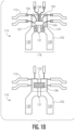
- FIGs. 1A-1B show respectively an example cross section view of an example semiconductor package and example surfaces of a simplified leadframe in the example semiconductor package according to an embodiment.
- the lead frame 102 may include a first surface 114 and an opposite second surface 116 which are planar surfaces of the lead frame 102.
- the leadframe 102 may be made of a conductive material such as copper, aluminum, or an alloy.
- the lead frame 102 may have a plurality of leads 110 and insertion terminals 118. In an example, six leads 110 are shown which terminate around a split die pad 120 of the leadframe 102 outlined by a dotted line.
- the leads 110 may be electrically coupled by a soldering or other process to a printed circuit board (not shown) or other substrate on which the semiconductor package 112 is mounted.
- the split die pad 120 may be split by a gap 121 of the leadframe 102 to form a first die pad side 122 and second die pad side 124, respectively, which are electrically isolated by a non-conductive material.
- the non-conductive material may be air before encapsulation and an encapsulant after encapsulation as described below.
- the split die pad 120 may support a semiconductor die 104.
- the semiconductor die 104 may be mounted on the split die pad 120 on a first surface 114 of the leadframe 102 and attached, for example, with a non-conductive adhesive such as an epoxy or adhesive tape.
- the semiconductor die 104 may be an integrated circuit such as a microprocessor that performs general processing or a dedicated circuit that performs a specific application such as motion sensing, pressure sensing, or speed sensing as examples.
- the leads 110 that terminate around the split die pad 120 may have respective bond pads 130.
- the semiconductor die 104 may be connected to the leads 110 by respective wires 108 from the semiconductor die 104 to the bond pads 130 on the leads 110.
- the insertion terminals 118 may include a first insertion terminal 126 and a second insertion terminal 128 which are integrated with the first die pad side 122 and second die pad side 124, respectively.
- the insertion terminals 118 may be arranged to be inserted in an insertion socket, through hole, or crimping mount (all not shown) which accepts the insertion terminals 118.
- the insertion socket, through hole, or crimping mount may be located on the printed circuit board or other substrate which the semiconductor package 112 is mounted on and further electrically coupled to additional circuitry such as a bus structure.
- the bus structure may allow communication between the semiconductor die 104 and yet additional circuitry coupled to the bus structure.
- the communication may include signals associated with the specific application of the integrated circuit and the yet additional circuitry may process the signals.
- a wire 108 may be coupled between a bond pad of the insertion terminals 118 and the semiconductor die 104 to provide for an electrical connection between the insertion terminals 118 to the semiconductor die 104.
- the semiconductor die 104 may receive or transmit signals via the insertion terminals 118 in an example.
- Embodiments disclosed herein are directed to mounting a component module 106 on the second surface 116 of the leadframe 102 which is opposite the first surface 114.
- the component module 106 may include one or more passive components such as resistors, capacitors, or inductors.
- the component module 106 may be mounted on the split die pad 120 of the lead frame 102 by a conductive adhesive such as an epoxy, adhesive tape, or solder.
- the component module 106 may be mounted directly opposite the semiconductor die 104 on the second surface 116.
- the components 136 of the component module 106 may perform a filtering of signals applied to the insertion terminals 118 by one or more of the semiconductor die 104 and the additional circuitry which is coupled to the socket, through hole, or crimping mount which accepts the insertion terminals 118. At least a portion of the leadframe 102 including the semiconductor die 104 and the component module 106 may then be encapsulated with an encapsulant 138 by a plastic (e.g., thermoset, thermoplastic) outlined by a dotted line and a molding process to form the semiconductor package 112.
- a plastic e.g., thermoset, thermoplastic
- the terminals 118 and the leads 110 may protrude from the encapsulant of the semiconductor package 112 to facilitate the electrical connections described above.
- FIG. 2 is an example of the component module 106 in accordance with an embodiment.
- a substrate 200 of the component module 106 may have a first surface 202 and a second surface 204.
- the substrate 200 may be a printed circuit board (PCB) in an example with conductive traces 212 that form an example circuit of passive components 210 such as capacitors (C) or resistors (R).
- passive components 210 On the first surface 202, passive components 210 may be mounted.
- the substrate 200 may have one or more electrical connections.
- one electrical connection 206 may be electrically coupled to the insertion terminal 126 and another electrical connection 208 may be electrically coupled to the insertion terminal 128 when the component module 106 is mounted over the split die 120 on the second surface 116 of the leadframe 102 opposite to where the semiconductor die 104 is mounted.
- the passive components 210 may perform a filtering of signals applied to the insertion terminals 118.
- the mounting of the component module 106 as described herein reduces a size of the semiconductor package 112 compared to directly mounting passive components on a conductive pattern on a leadframe and mounting the passive components on a same surface where a semiconductor die is mounted. Further, the arrangement disclosed herein allows for increasing density of the passive components 210 on the leadframe 102 compared to placing the passive components 136 directly on the conductive pattern of the leadframe 102 which limits a maximum density of passive components 210 on the leadframe 102. Additionally, the use of the component module 106 allows for different circuits of the passive components 210 to be realized and mounted to the leadframe 102 by changing the circuit on the substrate 200 and without having to change the conductive pattern of the leadframe 102 on which the passive components 210 would be otherwise directly mounted to.
- cost of materials to mount the component module 106 to the leadframe 102 may be less than cost to mount the passive components 136 directly to the leadframe.
- the component module 106 may be mounted to the leadframe 102 using a conductive epoxy, eutectic alloy, or solder which is less expensive than using materials such as a silver palladium alloy to mount the passive components 136 directly to the conductive pattern of the leadframe 102.
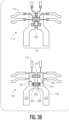
- FIGs. 3A-3B show respectively an example cross section view and example surfaces of a simplified leadframe 102 in an example semiconductor package 350 according to an embodiment.
- the leadframe 102 may further accommodate a two pole component 302 such as a battery in addition to the component module 106.
- the two pole device 302 may be mounted across the split die pad 120.
- One pole 304 of the two pole device 202 may be coupled to the first die pad side 122 and another pole 306 may be coupled to the second die pad side 124 of the leadframe 102 where the component module 106 is also mounted.
- a portion of the leadframe 102 which includes the semiconductor die 104, the two pole component 302, and the component module 106 may then be encapsulated with an encapsulant 138.
- the leadframe 102 allows for increased density of components by including both the component module 106 and the two pole device 202 in the semiconductor package 350.
- FIG. 4 is an example flow chart 400 of functions associated with manufacture of the semiconductor package 112 according to an embodiment.
- a semiconductor die 104 is mounted on a first surface 114 of a leadframe 102.
- the semiconductor die 104 may be coupled to leads 110 and insertion terminals 118 of the leadframe 102 by respective wires 108 from the semiconductor die 104 and affixed to bond pads 130 of the leads 110.
- the semiconductor die 104 may be mounted on a split die pad 120 of the leadframe 102 with a non-conductive adhesive in an example.
- a component module 106 may be mounted on a second surface 116 of the leadframe 102 opposite to the firsr surface 114.
- the component module 106 may be mounted on a split die pad 120 of the leadframe 102 and affixed by a conductive adhesive to the leadframe 102. At step 406, at least a portion of the leadframe 102 with the semiconductor die 104 and the component module 106 is encapsulated with an encapsulant 138.
- a semiconductor package comprises: a leadframe having a plurality of insertion terminals, a split die pad, and one or more leads; a component module having one or more passive components mounted on a substrate; a semiconductor die having an integrated circuit; wherein the component module is mounted on the split die pad at a first surface of the leadframe and forms an electrical connection with the insertion terminals and the semiconductor die is mounted on the split die pad at a second surface of the leadframe which is opposite to the first surface.
- the substrate is a printed circuit board comprising the one or more passive components, the printed circuit board having with a first contact which forms a first electrical connection of the component module with a first die pad side of the split die pad and a second contact which forms a second electrical connection of the component module with a second die pad side of the split die pad.
- the component module further comprises a conductive trace which couples the passive components to form a circuit of the passive components.
- the semiconductor package further comprises a two pole component mounted on the split die pad, wherein a first electrical connection of the two pole component forms an electrical connection with a first die pad side of the split die pad and a second electrical connection of the two pole component forms a second electrical connection with a second die pad side of the split die pad.
- the two pole component is a battery.
- the passive components are configured as a circuit.
- the split die pad has a first die pad side and a second die pad side separated by a gap of non-conductive material.
- the semiconductor package further comprises an encapsulant which encapsulates the semiconductor die, the component module, and at least a portion of the leadframe.
- the semiconductor package further comprises bond wires which form an electrical connection between the semiconductor die and respective bond pads of the one or more leads and the insertion leads.
- the component module is mounted to the leadframe by a conductive adhesive.
- the conductive adhesive is an epoxy.
- the leadframe is a conductive metal or alloy.
- a method of assembling a semiconductor package comprises: mounting a component module having one or more passive components on a split die pad at a first surface of a leadframe, the leadframe having a plurality of insertion terminals, a split die pad, and one or more leads, the mounted component module forms an electrical connection between the insertion terminals and the component module; mounting a semiconductor die having an integrated circuit on a split die pad at a second surface of the leadframe which is opposite to the first surface; and encapsulating one or more of the component module and the semiconductor die with an encapsulant to form the semiconductor package.
- the substrate is a printed circuit board comprising the one or more passive components, the printed circuit board having with a first contact which forms a first electrical connection of the component module with a first die pad side of the split die pad and a second contact which forms a second electrical connection of the component module with a second die pad side of the split die pad.
- the method further comprises mounting a two pole component on the split die pad, wherein a first electrical connection of the two pole component forms an electrical connection with a first die pad side of the split die pad and a second electrical connection forms an electrical connection with a second die pad side of the split die pad.
- the passive components are configured as a circuit.
- the split die pad has a first die pad side and a second die pad side separated by a gap of non-conductive material.
- encapsulating with the encapsulant comprises encapsulating at least a portion of the leadframe.
- the method further comprises connecting bond wires between the semiconductor die and respective bond pads of the one or more leads and the respective insertion terminals to electrically connect the semiconductor die to the one or more leads and the insertion terminals.
- mounting a component module comprises affixing the component module to the leadframe by a conductive adhesive.
Landscapes
- Lead Frames For Integrated Circuits (AREA)
Abstract
Description
- Embodiments of the subject matter described herein relate generally to a semiconductor package having a lead frame with semiconductor die and component module mounted on opposite surfaces of the lead frame and methods of manufacture thereof.
- A lead frame has a die pad for mounting a semiconductor die and leads surrounding the die pad. Each lead ends at respective die bond pad and bond wires connect the die to the respective bond pads. The lead frame is made of a conductive material such as copper or an alloy and customized with a conductive pattern to which passive components are directly mounted using materials such as a silver palladium alloy to form a circuit of the passive components. The lead frame also includes insertion terminals integrated with the conductive pattern. A portion of the lead frame is encapsulated with an encapsulant to form a semiconductor package and the insertion terminals inserted into a socket, through hole, or crimping mount which accepts the insertion terminals. The passive components facilitate filtering of signals between the semiconductor die of semiconductor package and circuitry coupled to the socket, through hole, or crimping mount which accepts the insertion terminals.
- A complete understanding of the subject matter may be derived by referring to the detailed description and claims when considered in conjunction with the following figures, wherein like reference numbers refer to similar elements throughout the figures.
-
FIGs. 1A-1B show respectively an example cross section view of an example semiconductor package and example surfaces of a simplified leadframe in the example semiconductor package according to an embodiment. -
FIG. 2 is an example of a component module in accordance with an embodiment. -
FIGs. 3A-3B show an example cross section view and example surfaces of a simplified leadframe in another example semiconductor package according to an embodiment. -
FIG. 4 is an example flow chart of functions associated with manufacturing the semiconductor package according to an embodiment. - Embodiments disclosed herein are directed to a semiconductor package having a lead frame with semiconductor die and component module mounted on opposite surfaces of the lead frame and methods of manufacture thereof. A semiconductor die is mounted on a split die pad of the lead frame on one surface of the lead frame and the component module is mounted on the split die pad on the other surface of the lead frame. The component module mounted on the other surface of the lead frame includes a substrate such as a printed circuit board on which passive components is mounted and coupled together by electrical connections such as traces on the substrate to form a circuit. The component module is further electrically coupled to the split die pad. A portion of the lead frame including the semiconductor die and the component module is encapsulated with an encapsulant such as a thermoplastic epoxy to form the semiconductor package. Well known structures and techniques have not been shown in detail in order not to obfuscate the description.
-
FIGs. 1A-1B show respectively an example cross section view of an example semiconductor package and example surfaces of a simplified leadframe in the example semiconductor package according to an embodiment. Thelead frame 102 may include afirst surface 114 and an oppositesecond surface 116 which are planar surfaces of thelead frame 102. In an example, theleadframe 102 may be made of a conductive material such as copper, aluminum, or an alloy. Further, thelead frame 102 may have a plurality ofleads 110 andinsertion terminals 118. In an example, sixleads 110 are shown which terminate around asplit die pad 120 of theleadframe 102 outlined by a dotted line. In an example, theleads 110 may be electrically coupled by a soldering or other process to a printed circuit board (not shown) or other substrate on which thesemiconductor package 112 is mounted. Thesplit die pad 120 may be split by agap 121 of theleadframe 102 to form a firstdie pad side 122 and seconddie pad side 124, respectively, which are electrically isolated by a non-conductive material. The non-conductive material may be air before encapsulation and an encapsulant after encapsulation as described below. The split diepad 120 may support asemiconductor die 104. In an example, the semiconductor die 104 may be mounted on the split diepad 120 on afirst surface 114 of theleadframe 102 and attached, for example, with a non-conductive adhesive such as an epoxy or adhesive tape. The semiconductor die 104 may be an integrated circuit such as a microprocessor that performs general processing or a dedicated circuit that performs a specific application such as motion sensing, pressure sensing, or speed sensing as examples. The leads 110 that terminate around the split diepad 120 may haverespective bond pads 130. In an example, the semiconductor die 104 may be connected to theleads 110 byrespective wires 108 from the semiconductor die 104 to thebond pads 130 on theleads 110. In an example, theinsertion terminals 118 may include afirst insertion terminal 126 and asecond insertion terminal 128 which are integrated with the firstdie pad side 122 and seconddie pad side 124, respectively. In an example, theinsertion terminals 118 may be arranged to be inserted in an insertion socket, through hole, or crimping mount (all not shown) which accepts theinsertion terminals 118. The insertion socket, through hole, or crimping mount may be located on the printed circuit board or other substrate which thesemiconductor package 112 is mounted on and further electrically coupled to additional circuitry such as a bus structure. The bus structure may allow communication between the semiconductor die 104 and yet additional circuitry coupled to the bus structure. In an example, the communication may include signals associated with the specific application of the integrated circuit and the yet additional circuitry may process the signals. Further, awire 108 may be coupled between a bond pad of theinsertion terminals 118 and the semiconductor die 104 to provide for an electrical connection between theinsertion terminals 118 to the semiconductor die 104. The semiconductor die 104 may receive or transmit signals via theinsertion terminals 118 in an example. - Embodiments disclosed herein are directed to mounting a
component module 106 on thesecond surface 116 of theleadframe 102 which is opposite thefirst surface 114. Thecomponent module 106 may include one or more passive components such as resistors, capacitors, or inductors. Thecomponent module 106 may be mounted on the split diepad 120 of thelead frame 102 by a conductive adhesive such as an epoxy, adhesive tape, or solder. In an example, thecomponent module 106 may be mounted directly opposite the semiconductor die 104 on thesecond surface 116. In an example, the components 136 of thecomponent module 106 may perform a filtering of signals applied to theinsertion terminals 118 by one or more of the semiconductor die 104 and the additional circuitry which is coupled to the socket, through hole, or crimping mount which accepts theinsertion terminals 118. At least a portion of theleadframe 102 including the semiconductor die 104 and thecomponent module 106 may then be encapsulated with anencapsulant 138 by a plastic (e.g., thermoset, thermoplastic) outlined by a dotted line and a molding process to form thesemiconductor package 112. In an example, theterminals 118 and theleads 110 may protrude from the encapsulant of thesemiconductor package 112 to facilitate the electrical connections described above. -
FIG. 2 is an example of thecomponent module 106 in accordance with an embodiment. Asubstrate 200 of thecomponent module 106 may have afirst surface 202 and asecond surface 204. Thesubstrate 200 may be a printed circuit board (PCB) in an example withconductive traces 212 that form an example circuit ofpassive components 210 such as capacitors (C) or resistors (R). On thefirst surface 202,passive components 210 may be mounted. Further, on thesecond surface 204, thesubstrate 200 may have one or more electrical connections. In an example, oneelectrical connection 206 may be electrically coupled to theinsertion terminal 126 and anotherelectrical connection 208 may be electrically coupled to theinsertion terminal 128 when thecomponent module 106 is mounted over the split die 120 on thesecond surface 116 of theleadframe 102 opposite to where the semiconductor die 104 is mounted. In an example, thepassive components 210 may perform a filtering of signals applied to theinsertion terminals 118. - The mounting of the
component module 106 as described herein reduces a size of thesemiconductor package 112 compared to directly mounting passive components on a conductive pattern on a leadframe and mounting the passive components on a same surface where a semiconductor die is mounted. Further, the arrangement disclosed herein allows for increasing density of thepassive components 210 on theleadframe 102 compared to placing the passive components 136 directly on the conductive pattern of theleadframe 102 which limits a maximum density ofpassive components 210 on theleadframe 102. Additionally, the use of thecomponent module 106 allows for different circuits of thepassive components 210 to be realized and mounted to theleadframe 102 by changing the circuit on thesubstrate 200 and without having to change the conductive pattern of theleadframe 102 on which thepassive components 210 would be otherwise directly mounted to. Still additionally, cost of materials to mount thecomponent module 106 to theleadframe 102 may be less than cost to mount the passive components 136 directly to the leadframe. Thecomponent module 106 may be mounted to theleadframe 102 using a conductive epoxy, eutectic alloy, or solder which is less expensive than using materials such as a silver palladium alloy to mount the passive components 136 directly to the conductive pattern of theleadframe 102. -
FIGs. 3A-3B show respectively an example cross section view and example surfaces of asimplified leadframe 102 in anexample semiconductor package 350 according to an embodiment. Theleadframe 102 may further accommodate a twopole component 302 such as a battery in addition to thecomponent module 106. The twopole device 302 may be mounted across the split diepad 120. Onepole 304 of the twopole device 202 may be coupled to the firstdie pad side 122 and anotherpole 306 may be coupled to the seconddie pad side 124 of theleadframe 102 where thecomponent module 106 is also mounted. A portion of theleadframe 102 which includes the semiconductor die 104, the twopole component 302, and thecomponent module 106 may then be encapsulated with anencapsulant 138. In an example, theleadframe 102 allows for increased density of components by including both thecomponent module 106 and the twopole device 202 in thesemiconductor package 350. -
FIG. 4 is anexample flow chart 400 of functions associated with manufacture of thesemiconductor package 112 according to an embodiment. Atstep 402, asemiconductor die 104 is mounted on afirst surface 114 of aleadframe 102. In examples, the semiconductor die 104 may be coupled toleads 110 andinsertion terminals 118 of theleadframe 102 byrespective wires 108 from the semiconductor die 104 and affixed tobond pads 130 of theleads 110. The semiconductor die 104 may be mounted on asplit die pad 120 of theleadframe 102 with a non-conductive adhesive in an example. Atstep 404, acomponent module 106 may be mounted on asecond surface 116 of theleadframe 102 opposite to thefirsr surface 114. Thecomponent module 106 may be mounted on asplit die pad 120 of theleadframe 102 and affixed by a conductive adhesive to theleadframe 102. Atstep 406, at least a portion of theleadframe 102 with the semiconductor die 104 and thecomponent module 106 is encapsulated with anencapsulant 138. - In one embodiment, a semiconductor package is disclosed. The semiconductor package comprises: a leadframe having a plurality of insertion terminals, a split die pad, and one or more leads; a component module having one or more passive components mounted on a substrate; a semiconductor die having an integrated circuit; wherein the component module is mounted on the split die pad at a first surface of the leadframe and forms an electrical connection with the insertion terminals and the semiconductor die is mounted on the split die pad at a second surface of the leadframe which is opposite to the first surface. In an embodiment, the substrate is a printed circuit board comprising the one or more passive components, the printed circuit board having with a first contact which forms a first electrical connection of the component module with a first die pad side of the split die pad and a second contact which forms a second electrical connection of the component module with a second die pad side of the split die pad. In an embodiment, the component module further comprises a conductive trace which couples the passive components to form a circuit of the passive components. In an embodiment, the semiconductor package further comprises a two pole component mounted on the split die pad, wherein a first electrical connection of the two pole component forms an electrical connection with a first die pad side of the split die pad and a second electrical connection of the two pole component forms a second electrical connection with a second die pad side of the split die pad. In an embodiment, the two pole component is a battery. In an embodiment, the passive components are configured as a circuit. In an embodiment, the split die pad has a first die pad side and a second die pad side separated by a gap of non-conductive material. In an embodiment, the semiconductor package further comprises an encapsulant which encapsulates the semiconductor die, the component module, and at least a portion of the leadframe. In an embodiment, the semiconductor package further comprises bond wires which form an electrical connection between the semiconductor die and respective bond pads of the one or more leads and the insertion leads. In an embodiment, the component module is mounted to the leadframe by a conductive adhesive. In an embodiment, the conductive adhesive is an epoxy. In an embodiment, the leadframe is a conductive metal or alloy.
- In another embodiment, a method of assembling a semiconductor package is disclosed. The method comprises: mounting a component module having one or more passive components on a split die pad at a first surface of a leadframe, the leadframe having a plurality of insertion terminals, a split die pad, and one or more leads, the mounted component module forms an electrical connection between the insertion terminals and the component module; mounting a semiconductor die having an integrated circuit on a split die pad at a second surface of the leadframe which is opposite to the first surface; and encapsulating one or more of the component module and the semiconductor die with an encapsulant to form the semiconductor package. In an embodiment, the substrate is a printed circuit board comprising the one or more passive components, the printed circuit board having with a first contact which forms a first electrical connection of the component module with a first die pad side of the split die pad and a second contact which forms a second electrical connection of the component module with a second die pad side of the split die pad. In an embodiment, the method further comprises mounting a two pole component on the split die pad, wherein a first electrical connection of the two pole component forms an electrical connection with a first die pad side of the split die pad and a second electrical connection forms an electrical connection with a second die pad side of the split die pad. In an embodiment, the passive components are configured as a circuit. In an embodiment, the split die pad has a first die pad side and a second die pad side separated by a gap of non-conductive material. In an embodiment, encapsulating with the encapsulant comprises encapsulating at least a portion of the leadframe. In an embodiment, the method further comprises connecting bond wires between the semiconductor die and respective bond pads of the one or more leads and the respective insertion terminals to electrically connect the semiconductor die to the one or more leads and the insertion terminals. In an embodiment, mounting a component module comprises affixing the component module to the leadframe by a conductive adhesive.
- For the sake of brevity, conventional semiconductor fabrication techniques may not be described in detail herein. In addition, certain terminology may also be used herein for reference only, and thus are not intended to be limiting, and the terms "first", "second" and other such numerical terms referring to structures do not imply a sequence or order unless clearly indicated by the context.
- The foregoing description refers to elements or nodes or features being "connected" or "coupled" together. As used herein, unless expressly stated otherwise, "connected" means that one element is directly joined to (or directly communicates with) another element, and not necessarily mechanically. Likewise, unless expressly stated otherwise, "coupled" means that one element is directly or indirectly joined to (or directly or indirectly communicates with) another element, and not necessarily mechanically. Thus, although the schematic shown in the figures depict one exemplary arrangement of elements, additional intervening elements, devices, features, or components may be present in an embodiment of the depicted subject matter.
- Although the operations of the method(s) herein are shown and described in a particular order, the order of the operations of each method may be altered so that certain operations may be performed in an inverse order or so that certain operations may be performed, at least in part, concurrently with other operations unless expressly indicated. In another embodiment, instructions or sub-operations of distinct operations may be implemented in an intermittent and/or alternating manner.
- While at least one exemplary embodiment has been presented in the foregoing detailed description, it should be appreciated that a vast number of variations exist. It should also be appreciated that the exemplary embodiment or embodiments described herein are not intended to limit the scope, applicability, or configuration of the claimed subject matter in any way. Rather, the foregoing detailed description will provide those skilled in the art with a convenient road map for implementing the described embodiment or embodiments. It should be understood that various changes can be made in the function and arrangement of elements without departing from the scope defined by the claims, which includes known equivalents and foreseeable equivalents at the time of filing this patent application.
Claims (15)
- A semiconductor package comprising:a leadframe having a plurality of insertion terminals, a split die pad, and one or more leads;a component module having one or more passive components mounted on a substrate;a semiconductor die having an integrated circuit;wherein the component module is mounted on the split die pad at a first surface of the leadframe and forms an electrical connection with the insertion terminals and the semiconductor die is mounted on the split die pad at a second surface of the leadframe which is opposite to the first surface.
- The semiconductor package of claim 1, wherein the substrate is a printed circuit board comprising the one or more passive components, the printed circuit board having with a first contact which forms a first electrical connection of the component module with a first die pad side of the split die pad and a second contact which forms a second electrical connection of the component module with a second die pad side of the split die pad.
- The semiconductor package of any of claims 1 to 2, wherein the component module further comprises a conductive trace which couples the passive components to form a circuit of the passive components.
- The semiconductor package of any of claims 1 to 3, further comprising a two pole component mounted on the split die pad, wherein a first electrical connection of the two pole component forms an electrical connection with a first die pad side of the split die pad and a second electrical connection of the two pole component forms a second electrical connection with a second die pad side of the split die pad.
- The semiconductor package of claim 4, wherein the two pole component is a battery.
- The semiconductor package of any of claims 1 to 5, wherein the passive components are configured as a circuit.
- The semiconductor package of any of claims 1 to 6, wherein the split die pad has a first die pad side and a second die pad side separated by a gap of non-conductive material.
- The semiconductor package of any of claims 1 to 7, further comprising an encapsulant which encapsulates the semiconductor die, the component module, and at least a portion of the leadframe.
- The semiconductor package of any of claims 1 to 8, further comprising bond wires which form an electrical connection between the semiconductor die and respective bond pads of the one or more leads and the insertion leads.
- The semiconductor package of any of claims 1 to 9, wherein the component module is mounted to the leadframe by a conductive adhesive.
- The semiconductor package of claim 10, wherein the conductive adhesive is an epoxy.
- The semiconductor package of any of claims 1 to 11, wherein the leadframe is a conductive metal or alloy.
- A method of assembling a semiconductor package comprising:mounting a component module having one or more passive components on a split die pad at a first surface of a leadframe, the leadframe having a plurality of insertion terminals, a split die pad, and one or more leads, the mounted component module forms an electrical connection between the insertion terminals and the component module;mounting a semiconductor die having an integrated circuit on a split die pad at a second surface of the leadframe which is opposite to the first surface; andencapsulating one or more of the component module and the semiconductor die with an encapsulant to form the semiconductor package.
- The method of claim 13, wherein the substrate is a printed circuit board comprising the one or more passive components, the printed circuit board having with a first contact which forms a first electrical connection of the component module with a first die pad side of the split die pad and a second contact which forms a second electrical connection of the component module with a second die pad side of the split die pad.
- The method of any of claims 13 to 14, further comprising mounting a two pole component on the split die pad, wherein a first electrical connection of the two pole component forms an electrical connection with a first die pad side of the split die pad and a second electrical connection forms an electrical connection with a second die pad side of the split die pad.
Applications Claiming Priority (1)
| Application Number | Priority Date | Filing Date | Title |
|---|---|---|---|
| US17/643,193 US12125771B2 (en) | 2021-12-08 | 2021-12-08 | Semiconductor package having lead frame with semiconductor die and component module mounted on opposite surfaces of the lead frame and methods of manufacture thereof |
Publications (2)
| Publication Number | Publication Date |
|---|---|
| EP4195261A1 true EP4195261A1 (en) | 2023-06-14 |
| EP4195261B1 EP4195261B1 (en) | 2026-01-07 |
Family
ID=84331734
Family Applications (1)
| Application Number | Title | Priority Date | Filing Date |
|---|---|---|---|
| EP22207302.5A Active EP4195261B1 (en) | 2021-12-08 | 2022-11-14 | Semiconductor package having lead frame with semiconductor die and component module mounted on opposite surfaces of the lead frame and methods of manufacture thereof |
Country Status (2)
| Country | Link |
|---|---|
| US (1) | US12125771B2 (en) |
| EP (1) | EP4195261B1 (en) |
Citations (3)
| Publication number | Priority date | Publication date | Assignee | Title |
|---|---|---|---|---|
| JPS6114731A (en) * | 1984-06-29 | 1986-01-22 | Nec Kansai Ltd | Semiconductor device |
| JPH01282853A (en) * | 1988-05-09 | 1989-11-14 | Mitsubishi Electric Corp | Semiconductor device |
| US20040094826A1 (en) * | 2002-09-20 | 2004-05-20 | Yang Chin An | Leadframe pakaging apparatus and packaging method thereof |
Family Cites Families (29)
| Publication number | Priority date | Publication date | Assignee | Title |
|---|---|---|---|---|
| US5012323A (en) * | 1989-11-20 | 1991-04-30 | Micron Technology, Inc. | Double-die semiconductor package having a back-bonded die and a face-bonded die interconnected on a single leadframe |
| US5689135A (en) * | 1995-12-19 | 1997-11-18 | Micron Technology, Inc. | Multi-chip device and method of fabrication employing leads over and under processes |
| US6531784B1 (en) * | 2000-06-02 | 2003-03-11 | Amkor Technology, Inc. | Semiconductor package with spacer strips |
| US6472758B1 (en) * | 2000-07-20 | 2002-10-29 | Amkor Technology, Inc. | Semiconductor package including stacked semiconductor dies and bond wires |
| US7416011B2 (en) | 2005-01-27 | 2008-08-26 | Delphi Technologies, Inc. | Electronic assembly having a substrate laminated within a backplate cavity |
| DE102005055761B4 (en) * | 2005-11-21 | 2008-02-07 | Infineon Technologies Ag | Power semiconductor component with semiconductor chip stack in bridge circuit and method for producing the same |
| US7535086B2 (en) * | 2006-08-03 | 2009-05-19 | Stats Chippac Ltd. | Integrated circuit package-on-package stacking system |
| US7843047B2 (en) * | 2008-11-21 | 2010-11-30 | Stats Chippac Ltd. | Encapsulant interposer system with integrated passive devices and manufacturing method therefor |
| US8062932B2 (en) * | 2008-12-01 | 2011-11-22 | Alpha & Omega Semiconductor, Inc. | Compact semiconductor package with integrated bypass capacitor and method |
| US8178954B2 (en) * | 2009-07-31 | 2012-05-15 | Alpha & Omega Semiconductor, Inc. | Structure of mixed semiconductor encapsulation structure with multiple chips and capacitors |
| US9257375B2 (en) * | 2009-07-31 | 2016-02-09 | Alpha and Omega Semiconductor Inc. | Multi-die semiconductor package |
| US20120326287A1 (en) * | 2011-06-27 | 2012-12-27 | National Semiconductor Corporation | Dc/dc convertor power module package incorporating a stacked controller and construction methodology |
| US8304887B2 (en) | 2009-12-10 | 2012-11-06 | Texas Instruments Incorporated | Module package with embedded substrate and leadframe |
| US8426952B2 (en) * | 2011-01-14 | 2013-04-23 | International Rectifier Corporation | Stacked half-bridge package with a common conductive leadframe |
| US8994157B1 (en) | 2011-05-27 | 2015-03-31 | Scientific Components Corporation | Circuit system in a package |
| US8643176B2 (en) * | 2011-07-27 | 2014-02-04 | Infineon Technologies Ag | Power semiconductor chip having two metal layers on one face |
| US8951847B2 (en) * | 2012-01-18 | 2015-02-10 | Intersil Americas LLC | Package leadframe for dual side assembly |
| US10128219B2 (en) * | 2012-04-25 | 2018-11-13 | Texas Instruments Incorporated | Multi-chip module including stacked power devices with metal clip |
| US9589929B2 (en) * | 2013-03-14 | 2017-03-07 | Vishay-Siliconix | Method for fabricating stack die package |
| US9966330B2 (en) * | 2013-03-14 | 2018-05-08 | Vishay-Siliconix | Stack die package |
| KR102337876B1 (en) * | 2014-06-10 | 2021-12-10 | 삼성전자주식회사 | Semiconductor package and method of manufacturing the same |
| US20180190776A1 (en) * | 2016-12-30 | 2018-07-05 | Sireesha Gogineni | Semiconductor chip package with cavity |
| US10943855B2 (en) * | 2017-08-23 | 2021-03-09 | Semiconductor Components Industries, Llc | Electronic device packaging with galvanic isolation |
| US11088055B2 (en) * | 2018-12-14 | 2021-08-10 | Texas Instruments Incorporated | Package with dies mounted on opposing surfaces of a leadframe |
| US11817438B2 (en) | 2019-01-14 | 2023-11-14 | Intel Corporationd | System in package with interconnected modules |
| US11158567B2 (en) * | 2019-08-09 | 2021-10-26 | Texas Instruments Incorporated | Package with stacked power stage and integrated control die |
| KR102729072B1 (en) * | 2019-08-28 | 2024-11-13 | 삼성전자주식회사 | Semiconductor package |
| US12074123B2 (en) * | 2020-04-03 | 2024-08-27 | Macom Technology Solutions Holdings, Inc. | Multi level radio frequency (RF) integrated circuit components including passive devices |
| US11562949B2 (en) * | 2020-06-17 | 2023-01-24 | Texas Instruments Incorporated | Semiconductor package including undermounted die with exposed backside metal |
-
2021
- 2021-12-08 US US17/643,193 patent/US12125771B2/en active Active
-
2022
- 2022-11-14 EP EP22207302.5A patent/EP4195261B1/en active Active
Patent Citations (3)
| Publication number | Priority date | Publication date | Assignee | Title |
|---|---|---|---|---|
| JPS6114731A (en) * | 1984-06-29 | 1986-01-22 | Nec Kansai Ltd | Semiconductor device |
| JPH01282853A (en) * | 1988-05-09 | 1989-11-14 | Mitsubishi Electric Corp | Semiconductor device |
| US20040094826A1 (en) * | 2002-09-20 | 2004-05-20 | Yang Chin An | Leadframe pakaging apparatus and packaging method thereof |
Also Published As
| Publication number | Publication date |
|---|---|
| US12125771B2 (en) | 2024-10-22 |
| US20230178457A1 (en) | 2023-06-08 |
| EP4195261B1 (en) | 2026-01-07 |
Similar Documents
| Publication | Publication Date | Title |
|---|---|---|
| EP2538761B1 (en) | Intelligent Power Module and related assembling method | |
| US6002165A (en) | Multilayered lead frame for semiconductor packages | |
| KR100600683B1 (en) | Semiconductor device and manufacturing method thereof | |
| US6482674B1 (en) | Semiconductor package having metal foil die mounting plate | |
| US8048719B2 (en) | Semiconductor device and manufacturing method thereof | |
| US20090152694A1 (en) | Electronic device | |
| US10707156B2 (en) | Electronic device | |
| EP0729646B1 (en) | Electronic system circuit package | |
| EP1520296B1 (en) | Wearable silicon chip | |
| US10790220B2 (en) | Press-fit semiconductor device | |
| JPH08306723A (en) | Electronic circuit board and manufacturing method thereof | |
| JPH05121644A (en) | Electronic circuit device | |
| EP1636840B1 (en) | Micro lead frame substrate and method for its manufacture | |
| US12513870B2 (en) | Power module | |
| US12125771B2 (en) | Semiconductor package having lead frame with semiconductor die and component module mounted on opposite surfaces of the lead frame and methods of manufacture thereof | |
| US9117807B2 (en) | Integrated passives package, semiconductor module and method of manufacturing | |
| US20250212334A1 (en) | Semiconductor module | |
| JP2737332B2 (en) | Integrated circuit device | |
| JP4311294B2 (en) | Electronic device and manufacturing method thereof | |
| CN120237128A (en) | Electronic package with lid containing battery | |
| JPH0685165A (en) | Semiconductor device and manufacture thereof | |
| US20200035577A1 (en) | Packaged integrated circuit | |
| JPH07169795A (en) | Semiconductor device | |
| JPH04239161A (en) | Resin-sealed type semiconductor device | |
| JPH08204305A (en) | Hybrid integrated circuit device |
Legal Events
| Date | Code | Title | Description |
|---|---|---|---|
| PUAI | Public reference made under article 153(3) epc to a published international application that has entered the european phase |
Free format text: ORIGINAL CODE: 0009012 |
|
| STAA | Information on the status of an ep patent application or granted ep patent |
Free format text: STATUS: THE APPLICATION HAS BEEN PUBLISHED |
|
| AK | Designated contracting states |
Kind code of ref document: A1 Designated state(s): AL AT BE BG CH CY CZ DE DK EE ES FI FR GB GR HR HU IE IS IT LI LT LU LV MC ME MK MT NL NO PL PT RO RS SE SI SK SM TR |
|
| STAA | Information on the status of an ep patent application or granted ep patent |
Free format text: STATUS: REQUEST FOR EXAMINATION WAS MADE |
|
| 17P | Request for examination filed |
Effective date: 20231214 |
|
| RBV | Designated contracting states (corrected) |
Designated state(s): AL AT BE BG CH CY CZ DE DK EE ES FI FR GB GR HR HU IE IS IT LI LT LU LV MC ME MK MT NL NO PL PT RO RS SE SI SK SM TR |
|
| GRAP | Despatch of communication of intention to grant a patent |
Free format text: ORIGINAL CODE: EPIDOSNIGR1 |
|
| STAA | Information on the status of an ep patent application or granted ep patent |
Free format text: STATUS: GRANT OF PATENT IS INTENDED |
|
| INTG | Intention to grant announced |
Effective date: 20251006 |
|
| GRAS | Grant fee paid |
Free format text: ORIGINAL CODE: EPIDOSNIGR3 |
|
| GRAA | (expected) grant |
Free format text: ORIGINAL CODE: 0009210 |
|
| STAA | Information on the status of an ep patent application or granted ep patent |
Free format text: STATUS: THE PATENT HAS BEEN GRANTED |
|
| AK | Designated contracting states |
Kind code of ref document: B1 Designated state(s): AL AT BE BG CH CY CZ DE DK EE ES FI FR GB GR HR HU IE IS IT LI LT LU LV MC ME MK MT NL NO PL PT RO RS SE SI SK SM TR |
|
| REG | Reference to a national code |
Ref country code: CH Ref legal event code: F10 Free format text: ST27 STATUS EVENT CODE: U-0-0-F10-F00 (AS PROVIDED BY THE NATIONAL OFFICE) Effective date: 20260107 Ref country code: GB Ref legal event code: FG4D |
|
| REG | Reference to a national code |
Ref country code: DE Ref legal event code: R096 Ref document number: 602022028326 Country of ref document: DE |
|
| REG | Reference to a national code |
Ref country code: IE Ref legal event code: FG4D |
|
| REG | Reference to a national code |
Ref country code: NL Ref legal event code: MP Effective date: 20260107 |
|
| PG25 | Lapsed in a contracting state [announced via postgrant information from national office to epo] |
Ref country code: NL Free format text: LAPSE BECAUSE OF FAILURE TO SUBMIT A TRANSLATION OF THE DESCRIPTION OR TO PAY THE FEE WITHIN THE PRESCRIBED TIME-LIMIT Effective date: 20260107 |
|
| REG | Reference to a national code |
Ref country code: AT Ref legal event code: MK05 Ref document number: 1876182 Country of ref document: AT Kind code of ref document: T Effective date: 20260107 |
|
| PG25 | Lapsed in a contracting state [announced via postgrant information from national office to epo] |
Ref country code: RS Free format text: LAPSE BECAUSE OF FAILURE TO SUBMIT A TRANSLATION OF THE DESCRIPTION OR TO PAY THE FEE WITHIN THE PRESCRIBED TIME-LIMIT Effective date: 20260407 |
|
| PG25 | Lapsed in a contracting state [announced via postgrant information from national office to epo] |
Ref country code: ES Free format text: LAPSE BECAUSE OF FAILURE TO SUBMIT A TRANSLATION OF THE DESCRIPTION OR TO PAY THE FEE WITHIN THE PRESCRIBED TIME-LIMIT Effective date: 20260107 |
|
| PG25 | Lapsed in a contracting state [announced via postgrant information from national office to epo] |
Ref country code: PL Free format text: LAPSE BECAUSE OF FAILURE TO SUBMIT A TRANSLATION OF THE DESCRIPTION OR TO PAY THE FEE WITHIN THE PRESCRIBED TIME-LIMIT Effective date: 20260107 |
|
| PG25 | Lapsed in a contracting state [announced via postgrant information from national office to epo] |
Ref country code: GR Free format text: LAPSE BECAUSE OF FAILURE TO SUBMIT A TRANSLATION OF THE DESCRIPTION OR TO PAY THE FEE WITHIN THE PRESCRIBED TIME-LIMIT Effective date: 20260408 |
|
| REG | Reference to a national code |
Ref country code: LT Ref legal event code: MG9D |
|
| PG25 | Lapsed in a contracting state [announced via postgrant information from national office to epo] |
Ref country code: LT Free format text: LAPSE BECAUSE OF FAILURE TO SUBMIT A TRANSLATION OF THE DESCRIPTION OR TO PAY THE FEE WITHIN THE PRESCRIBED TIME-LIMIT Effective date: 20260107 |
|
| PG25 | Lapsed in a contracting state [announced via postgrant information from national office to epo] |
Ref country code: NO Free format text: LAPSE BECAUSE OF FAILURE TO SUBMIT A TRANSLATION OF THE DESCRIPTION OR TO PAY THE FEE WITHIN THE PRESCRIBED TIME-LIMIT Effective date: 20260407 |
|
| PG25 | Lapsed in a contracting state [announced via postgrant information from national office to epo] |
Ref country code: SE Free format text: LAPSE BECAUSE OF FAILURE TO SUBMIT A TRANSLATION OF THE DESCRIPTION OR TO PAY THE FEE WITHIN THE PRESCRIBED TIME-LIMIT Effective date: 20260107 Ref country code: AT Free format text: LAPSE BECAUSE OF FAILURE TO SUBMIT A TRANSLATION OF THE DESCRIPTION OR TO PAY THE FEE WITHIN THE PRESCRIBED TIME-LIMIT Effective date: 20260107 Ref country code: FI Free format text: LAPSE BECAUSE OF FAILURE TO SUBMIT A TRANSLATION OF THE DESCRIPTION OR TO PAY THE FEE WITHIN THE PRESCRIBED TIME-LIMIT Effective date: 20260107 |
|
| PG25 | Lapsed in a contracting state [announced via postgrant information from national office to epo] |
Ref country code: HR Free format text: LAPSE BECAUSE OF FAILURE TO SUBMIT A TRANSLATION OF THE DESCRIPTION OR TO PAY THE FEE WITHIN THE PRESCRIBED TIME-LIMIT Effective date: 20260107 |
|
| PG25 | Lapsed in a contracting state [announced via postgrant information from national office to epo] |
Ref country code: IS Free format text: LAPSE BECAUSE OF FAILURE TO SUBMIT A TRANSLATION OF THE DESCRIPTION OR TO PAY THE FEE WITHIN THE PRESCRIBED TIME-LIMIT Effective date: 20260507 Ref country code: PT Free format text: LAPSE BECAUSE OF FAILURE TO SUBMIT A TRANSLATION OF THE DESCRIPTION OR TO PAY THE FEE WITHIN THE PRESCRIBED TIME-LIMIT Effective date: 20260507 |
|
| PG25 | Lapsed in a contracting state [announced via postgrant information from national office to epo] |
Ref country code: LV Free format text: LAPSE BECAUSE OF FAILURE TO SUBMIT A TRANSLATION OF THE DESCRIPTION OR TO PAY THE FEE WITHIN THE PRESCRIBED TIME-LIMIT Effective date: 20260107 |
|
| PG25 | Lapsed in a contracting state [announced via postgrant information from national office to epo] |
Ref country code: BG Free format text: LAPSE BECAUSE OF FAILURE TO SUBMIT A TRANSLATION OF THE DESCRIPTION OR TO PAY THE FEE WITHIN THE PRESCRIBED TIME-LIMIT Effective date: 20260107 |