EP4195260A2 - Transistor with odd-mode oscillation stabilization circuit - Google Patents
Transistor with odd-mode oscillation stabilization circuit Download PDFInfo
- Publication number
- EP4195260A2 EP4195260A2 EP22204791.2A EP22204791A EP4195260A2 EP 4195260 A2 EP4195260 A2 EP 4195260A2 EP 22204791 A EP22204791 A EP 22204791A EP 4195260 A2 EP4195260 A2 EP 4195260A2
- Authority
- EP
- European Patent Office
- Prior art keywords
- coupled
- bond pad
- conductive structure
- transistor
- conductive
- Prior art date
- Legal status (The legal status is an assumption and is not a legal conclusion. Google has not performed a legal analysis and makes no representation as to the accuracy of the status listed.)
- Pending
Links
- 230000010355 oscillation Effects 0.000 title claims abstract description 32
- 230000006641 stabilisation Effects 0.000 title claims abstract description 22
- 238000011105 stabilization Methods 0.000 title claims abstract description 22
- 239000000758 substrate Substances 0.000 claims abstract description 74
- 239000004065 semiconductor Substances 0.000 claims abstract description 37
- 239000000463 material Substances 0.000 claims description 14
- 230000003321 amplification Effects 0.000 description 16
- 238000003199 nucleic acid amplification method Methods 0.000 description 16
- 230000010363 phase shift Effects 0.000 description 16
- JMASRVWKEDWRBT-UHFFFAOYSA-N Gallium nitride Chemical compound [Ga]#N JMASRVWKEDWRBT-UHFFFAOYSA-N 0.000 description 5
- 229910002601 GaN Inorganic materials 0.000 description 4
- 238000012986 modification Methods 0.000 description 4
- 230000004048 modification Effects 0.000 description 4
- 230000008901 benefit Effects 0.000 description 3
- 230000005540 biological transmission Effects 0.000 description 3
- 239000012212 insulator Substances 0.000 description 3
- JBRZTFJDHDCESZ-UHFFFAOYSA-N AsGa Chemical compound [As]#[Ga] JBRZTFJDHDCESZ-UHFFFAOYSA-N 0.000 description 2
- 239000003990 capacitor Substances 0.000 description 2
- 239000002131 composite material Substances 0.000 description 2
- 230000001186 cumulative effect Effects 0.000 description 2
- 230000003111 delayed effect Effects 0.000 description 2
- 230000005669 field effect Effects 0.000 description 2
- 230000012447 hatching Effects 0.000 description 2
- 230000017525 heat dissipation Effects 0.000 description 2
- 238000000034 method Methods 0.000 description 2
- 229910021420 polycrystalline silicon Inorganic materials 0.000 description 2
- 229920005591 polysilicon Polymers 0.000 description 2
- 229910001218 Gallium arsenide Inorganic materials 0.000 description 1
- XUIMIQQOPSSXEZ-UHFFFAOYSA-N Silicon Chemical compound [Si] XUIMIQQOPSSXEZ-UHFFFAOYSA-N 0.000 description 1
- 230000009286 beneficial effect Effects 0.000 description 1
- 230000001419 dependent effect Effects 0.000 description 1
- 238000000151 deposition Methods 0.000 description 1
- 230000001627 detrimental effect Effects 0.000 description 1
- 238000010586 diagram Methods 0.000 description 1
- 239000008393 encapsulating agent Substances 0.000 description 1
- 238000005530 etching Methods 0.000 description 1
- 229910052751 metal Inorganic materials 0.000 description 1
- 239000002184 metal Substances 0.000 description 1
- 238000000059 patterning Methods 0.000 description 1
- 230000003014 reinforcing effect Effects 0.000 description 1
- 229910052594 sapphire Inorganic materials 0.000 description 1
- 239000010980 sapphire Substances 0.000 description 1
- 230000011218 segmentation Effects 0.000 description 1
- 238000000926 separation method Methods 0.000 description 1
- 229910052710 silicon Inorganic materials 0.000 description 1
- 239000010703 silicon Substances 0.000 description 1
- HBMJWWWQQXIZIP-UHFFFAOYSA-N silicon carbide Chemical compound [Si+]#[C-] HBMJWWWQQXIZIP-UHFFFAOYSA-N 0.000 description 1
- 229910010271 silicon carbide Inorganic materials 0.000 description 1
- 230000003595 spectral effect Effects 0.000 description 1
- 230000000087 stabilizing effect Effects 0.000 description 1
Images


Classifications
-
- H—ELECTRICITY
- H01—ELECTRIC ELEMENTS
- H01L—SEMICONDUCTOR DEVICES NOT COVERED BY CLASS H10
- H01L27/00—Devices consisting of a plurality of semiconductor or other solid-state components formed in or on a common substrate
- H01L27/02—Devices consisting of a plurality of semiconductor or other solid-state components formed in or on a common substrate including semiconductor components specially adapted for rectifying, oscillating, amplifying or switching and having at least one potential-jump barrier or surface barrier; including integrated passive circuit elements with at least one potential-jump barrier or surface barrier
- H01L27/04—Devices consisting of a plurality of semiconductor or other solid-state components formed in or on a common substrate including semiconductor components specially adapted for rectifying, oscillating, amplifying or switching and having at least one potential-jump barrier or surface barrier; including integrated passive circuit elements with at least one potential-jump barrier or surface barrier the substrate being a semiconductor body
- H01L27/06—Devices consisting of a plurality of semiconductor or other solid-state components formed in or on a common substrate including semiconductor components specially adapted for rectifying, oscillating, amplifying or switching and having at least one potential-jump barrier or surface barrier; including integrated passive circuit elements with at least one potential-jump barrier or surface barrier the substrate being a semiconductor body including a plurality of individual components in a non-repetitive configuration
- H01L27/0611—Devices consisting of a plurality of semiconductor or other solid-state components formed in or on a common substrate including semiconductor components specially adapted for rectifying, oscillating, amplifying or switching and having at least one potential-jump barrier or surface barrier; including integrated passive circuit elements with at least one potential-jump barrier or surface barrier the substrate being a semiconductor body including a plurality of individual components in a non-repetitive configuration integrated circuits having a two-dimensional layout of components without a common active region
- H01L27/0617—Devices consisting of a plurality of semiconductor or other solid-state components formed in or on a common substrate including semiconductor components specially adapted for rectifying, oscillating, amplifying or switching and having at least one potential-jump barrier or surface barrier; including integrated passive circuit elements with at least one potential-jump barrier or surface barrier the substrate being a semiconductor body including a plurality of individual components in a non-repetitive configuration integrated circuits having a two-dimensional layout of components without a common active region comprising components of the field-effect type
- H01L27/0629—Devices consisting of a plurality of semiconductor or other solid-state components formed in or on a common substrate including semiconductor components specially adapted for rectifying, oscillating, amplifying or switching and having at least one potential-jump barrier or surface barrier; including integrated passive circuit elements with at least one potential-jump barrier or surface barrier the substrate being a semiconductor body including a plurality of individual components in a non-repetitive configuration integrated circuits having a two-dimensional layout of components without a common active region comprising components of the field-effect type in combination with diodes, or resistors, or capacitors
-
- H—ELECTRICITY
- H01—ELECTRIC ELEMENTS
- H01L—SEMICONDUCTOR DEVICES NOT COVERED BY CLASS H10
- H01L23/00—Details of semiconductor or other solid state devices
- H01L23/48—Arrangements for conducting electric current to or from the solid state body in operation, e.g. leads, terminal arrangements ; Selection of materials therefor
- H01L23/482—Arrangements for conducting electric current to or from the solid state body in operation, e.g. leads, terminal arrangements ; Selection of materials therefor consisting of lead-in layers inseparably applied to the semiconductor body
- H01L23/4824—Pads with extended contours, e.g. grid structure, branch structure, finger structure
-
- H—ELECTRICITY
- H01—ELECTRIC ELEMENTS
- H01L—SEMICONDUCTOR DEVICES NOT COVERED BY CLASS H10
- H01L27/00—Devices consisting of a plurality of semiconductor or other solid-state components formed in or on a common substrate
- H01L27/02—Devices consisting of a plurality of semiconductor or other solid-state components formed in or on a common substrate including semiconductor components specially adapted for rectifying, oscillating, amplifying or switching and having at least one potential-jump barrier or surface barrier; including integrated passive circuit elements with at least one potential-jump barrier or surface barrier
- H01L27/0203—Particular design considerations for integrated circuits
- H01L27/0207—Geometrical layout of the components, e.g. computer aided design; custom LSI, semi-custom LSI, standard cell technique
-
- H—ELECTRICITY
- H01—ELECTRIC ELEMENTS
- H01L—SEMICONDUCTOR DEVICES NOT COVERED BY CLASS H10
- H01L23/00—Details of semiconductor or other solid state devices
- H01L23/48—Arrangements for conducting electric current to or from the solid state body in operation, e.g. leads, terminal arrangements ; Selection of materials therefor
- H01L23/481—Internal lead connections, e.g. via connections, feedthrough structures
-
- H—ELECTRICITY
- H01—ELECTRIC ELEMENTS
- H01L—SEMICONDUCTOR DEVICES NOT COVERED BY CLASS H10
- H01L23/00—Details of semiconductor or other solid state devices
- H01L23/58—Structural electrical arrangements for semiconductor devices not otherwise provided for, e.g. in combination with batteries
- H01L23/64—Impedance arrangements
- H01L23/66—High-frequency adaptations
-
- H—ELECTRICITY
- H01—ELECTRIC ELEMENTS
- H01L—SEMICONDUCTOR DEVICES NOT COVERED BY CLASS H10
- H01L24/00—Arrangements for connecting or disconnecting semiconductor or solid-state bodies; Methods or apparatus related thereto
- H01L24/01—Means for bonding being attached to, or being formed on, the surface to be connected, e.g. chip-to-package, die-attach, "first-level" interconnects; Manufacturing methods related thereto
- H01L24/02—Bonding areas ; Manufacturing methods related thereto
- H01L24/04—Structure, shape, material or disposition of the bonding areas prior to the connecting process
- H01L24/05—Structure, shape, material or disposition of the bonding areas prior to the connecting process of an individual bonding area
-
- H—ELECTRICITY
- H01—ELECTRIC ELEMENTS
- H01L—SEMICONDUCTOR DEVICES NOT COVERED BY CLASS H10
- H01L29/00—Semiconductor devices adapted for rectifying, amplifying, oscillating or switching, or capacitors or resistors with at least one potential-jump barrier or surface barrier, e.g. PN junction depletion layer or carrier concentration layer; Details of semiconductor bodies or of electrodes thereof ; Multistep manufacturing processes therefor
- H01L29/40—Electrodes ; Multistep manufacturing processes therefor
- H01L29/41—Electrodes ; Multistep manufacturing processes therefor characterised by their shape, relative sizes or dispositions
- H01L29/423—Electrodes ; Multistep manufacturing processes therefor characterised by their shape, relative sizes or dispositions not carrying the current to be rectified, amplified or switched
- H01L29/42312—Gate electrodes for field effect devices
- H01L29/42316—Gate electrodes for field effect devices for field-effect transistors
- H01L29/4232—Gate electrodes for field effect devices for field-effect transistors with insulated gate
- H01L29/42372—Gate electrodes for field effect devices for field-effect transistors with insulated gate characterised by the conducting layer, e.g. the length, the sectional shape or the lay-out
- H01L29/42376—Gate electrodes for field effect devices for field-effect transistors with insulated gate characterised by the conducting layer, e.g. the length, the sectional shape or the lay-out characterised by the length or the sectional shape
-
- H—ELECTRICITY
- H01—ELECTRIC ELEMENTS
- H01L—SEMICONDUCTOR DEVICES NOT COVERED BY CLASS H10
- H01L29/00—Semiconductor devices adapted for rectifying, amplifying, oscillating or switching, or capacitors or resistors with at least one potential-jump barrier or surface barrier, e.g. PN junction depletion layer or carrier concentration layer; Details of semiconductor bodies or of electrodes thereof ; Multistep manufacturing processes therefor
- H01L29/40—Electrodes ; Multistep manufacturing processes therefor
- H01L29/41—Electrodes ; Multistep manufacturing processes therefor characterised by their shape, relative sizes or dispositions
- H01L29/423—Electrodes ; Multistep manufacturing processes therefor characterised by their shape, relative sizes or dispositions not carrying the current to be rectified, amplified or switched
- H01L29/42312—Gate electrodes for field effect devices
- H01L29/42316—Gate electrodes for field effect devices for field-effect transistors
- H01L29/4232—Gate electrodes for field effect devices for field-effect transistors with insulated gate
- H01L29/42372—Gate electrodes for field effect devices for field-effect transistors with insulated gate characterised by the conducting layer, e.g. the length, the sectional shape or the lay-out
- H01L29/4238—Gate electrodes for field effect devices for field-effect transistors with insulated gate characterised by the conducting layer, e.g. the length, the sectional shape or the lay-out characterised by the surface lay-out
-
- H—ELECTRICITY
- H01—ELECTRIC ELEMENTS
- H01L—SEMICONDUCTOR DEVICES NOT COVERED BY CLASS H10
- H01L29/00—Semiconductor devices adapted for rectifying, amplifying, oscillating or switching, or capacitors or resistors with at least one potential-jump barrier or surface barrier, e.g. PN junction depletion layer or carrier concentration layer; Details of semiconductor bodies or of electrodes thereof ; Multistep manufacturing processes therefor
- H01L29/66—Types of semiconductor device ; Multistep manufacturing processes therefor
- H01L29/68—Types of semiconductor device ; Multistep manufacturing processes therefor controllable by only the electric current supplied, or only the electric potential applied, to an electrode which does not carry the current to be rectified, amplified or switched
- H01L29/76—Unipolar devices, e.g. field effect transistors
- H01L29/772—Field effect transistors
- H01L29/78—Field effect transistors with field effect produced by an insulated gate
-
- H—ELECTRICITY
- H03—ELECTRONIC CIRCUITRY
- H03F—AMPLIFIERS
- H03F1/00—Details of amplifiers with only discharge tubes, only semiconductor devices or only unspecified devices as amplifying elements
- H03F1/02—Modifications of amplifiers to raise the efficiency, e.g. gliding Class A stages, use of an auxiliary oscillation
- H03F1/0205—Modifications of amplifiers to raise the efficiency, e.g. gliding Class A stages, use of an auxiliary oscillation in transistor amplifiers
- H03F1/0288—Modifications of amplifiers to raise the efficiency, e.g. gliding Class A stages, use of an auxiliary oscillation in transistor amplifiers using a main and one or several auxiliary peaking amplifiers whereby the load is connected to the main amplifier using an impedance inverter, e.g. Doherty amplifiers
-
- H—ELECTRICITY
- H03—ELECTRONIC CIRCUITRY
- H03F—AMPLIFIERS
- H03F3/00—Amplifiers with only discharge tubes or only semiconductor devices as amplifying elements
- H03F3/189—High frequency amplifiers, e.g. radio frequency amplifiers
- H03F3/19—High frequency amplifiers, e.g. radio frequency amplifiers with semiconductor devices only
- H03F3/195—High frequency amplifiers, e.g. radio frequency amplifiers with semiconductor devices only in integrated circuits
-
- H—ELECTRICITY
- H01—ELECTRIC ELEMENTS
- H01L—SEMICONDUCTOR DEVICES NOT COVERED BY CLASS H10
- H01L2223/00—Details relating to semiconductor or other solid state devices covered by the group H01L23/00
- H01L2223/58—Structural electrical arrangements for semiconductor devices not otherwise provided for
- H01L2223/64—Impedance arrangements
- H01L2223/66—High-frequency adaptations
- H01L2223/6644—Packaging aspects of high-frequency amplifiers
- H01L2223/665—Bias feed arrangements
-
- H—ELECTRICITY
- H01—ELECTRIC ELEMENTS
- H01L—SEMICONDUCTOR DEVICES NOT COVERED BY CLASS H10
- H01L2223/00—Details relating to semiconductor or other solid state devices covered by the group H01L23/00
- H01L2223/58—Structural electrical arrangements for semiconductor devices not otherwise provided for
- H01L2223/64—Impedance arrangements
- H01L2223/66—High-frequency adaptations
- H01L2223/6644—Packaging aspects of high-frequency amplifiers
- H01L2223/6655—Matching arrangements, e.g. arrangement of inductive and capacitive components
-
- H—ELECTRICITY
- H01—ELECTRIC ELEMENTS
- H01L—SEMICONDUCTOR DEVICES NOT COVERED BY CLASS H10
- H01L2224/00—Indexing scheme for arrangements for connecting or disconnecting semiconductor or solid-state bodies and methods related thereto as covered by H01L24/00
- H01L2224/01—Means for bonding being attached to, or being formed on, the surface to be connected, e.g. chip-to-package, die-attach, "first-level" interconnects; Manufacturing methods related thereto
- H01L2224/02—Bonding areas; Manufacturing methods related thereto
- H01L2224/04—Structure, shape, material or disposition of the bonding areas prior to the connecting process
- H01L2224/05—Structure, shape, material or disposition of the bonding areas prior to the connecting process of an individual bonding area
- H01L2224/0554—External layer
- H01L2224/0555—Shape
-
- H—ELECTRICITY
- H03—ELECTRONIC CIRCUITRY
- H03F—AMPLIFIERS
- H03F2200/00—Indexing scheme relating to amplifiers
- H03F2200/451—Indexing scheme relating to amplifiers the amplifier being a radio frequency amplifier
Abstract
Description
- The present invention relates generally to transistors. More specifically, the present invention relates to a transistor layout utilizing a circuit configured to stabilize odd-mode oscillations in the transistor during operation.
- Radio Frequency (RF) power transistors that are sufficiently large relative to the wavelength of their maximum frequency of operation may be vulnerable to odd-mode instability, which is a phenomenon in which an undesirable oscillation becomes established in the transistor as a resonance between different parts of the transistor itself. This resonance can be viewed as a signal being amplified as it travels laterally from one end of the device to the other end and then back, reinforcing itself with each round trip. Besides just physical size and maximum operating frequency, other factors also can be relevant to whether significant odd-mode oscillations will occur within a transistor. In order to reduce or eliminate detrimental effects on transistor performance associated with odd-mode oscillations, designers strive to design transistors in which significant odd-mode oscillations are less likely to occur.
- The accompanying figures in which like reference numerals refer to identical or functionally similar elements throughout the separate views, the figures are not necessarily drawn to scale, and which together with the detailed description below are incorporated in and form part of the specification, serve to further illustrate various embodiments and to explain various principles and advantages all in accordance with the present invention.
-
FIG. 1 shows a schematic of a common source field effect transistor (FET) circuit configuration; -
FIG. 2 shows a top view of a layout of a prior art FET cell; -
FIG. 3 shows a top view of a layout of another prior art FET cell; -
FIGs 4A, 4B ,4C, and 4D (referred to collectively asFIG. 4 ) show top, partial top, and cross-sectional views of a layout of a FET cell in accordance with an embodiment of the present invention; -
FIG. 5 shows a top view of a FET that includes multiple instances of the FET cell ofFIG. 4 ; -
FIG. 6 shows a schematic diagram of an amplifier, in accordance with an example embodiment of the present invention; and -
FIG. 7 shows a top view of an amplifier module, in accordance with an example embodiment of the present invention. - An RF power transistor includes a semiconductor die with a plurality of interdigitated, elongated source and drain regions, along with elongated channel regions located between adjacent source and drain regions. The source regions are electrically connected to a ground reference (e.g., a conductive layer on the back side of the transistor die) using through substrate vias. The drain regions are contacted by elongated, conductive drain terminals, and an output end of each drain terminal is electrically connected to a drain bond pad (also referred to as an "output" bond pad herein), which extends perpendicularly to the drain terminals. The drain bond pad functions to combine the signals produced by the drain terminals, and serves as the output terminal for the power transistor. An elongated gate structure overlies each channel region, and an RF signal applied to the gate structures varies the electrical conductivity of the channels, thus varying the amount of current flowing between sets of adjacent source and drain regions. An input end of each gate structure is connected to a gate bond pad (also referred to as an "input" bond pad herein), and the gate bond pad is configured to receive an input RF signal for amplification, and to convey that signal to the gate structures. During operation, an amplified version of the input RF signal is produced at the drain bond pad.
- As discussed above, RF power transistors that are sufficiently large relative to the wavelength of their maximum frequency of operation may be vulnerable to odd-mode instability due to odd-mode oscillations that occur during operation. As will be described in greater detail later, embodiments of the inventive subject matter each include an RF power transistor that includes an odd-mode oscillation stabilization circuit.
- The instant disclosure is provided to further explain in an enabling fashion at least one embodiment in accordance with the present invention. The disclosure is further offered to enhance an understanding and appreciation for the inventive principles and advantages thereof, rather than to limit in any manner the invention. The invention is defined solely by the appended claims including any amendments made during the pendency of this application and all equivalents of those claims as issued.
- It should be understood that the use of relational terms, if any, such as first and second, top and bottom, and the like are used solely to distinguish one from another entity or action without necessarily requiring or implying any actual such relationship or order between such entities or actions. Furthermore, some of the figures may be illustrated using various shading and/or hatching to distinguish the different elements produced within the various structural layers. These different elements within the structural layers may be produced utilizing current and upcoming microfabrication techniques of depositing, patterning, etching, and so forth. Accordingly, although different shading and/or hatching is utilized in the illustrations, the different elements within the structural layers may be formed out of the same material.
- Referring to
FIG. 1, FIG. 1 shows a schematic of a common source field-effect transistor (FET)device configuration 100. In commonsource FET configuration 100, the gate, G, serves as aninput port 122 and the drain, D, serves as anoutput port 124. The source, S, serves as acommon connection 126 incommon source configuration 100 since the source is grounded as shown inFIG. 1 . Thus,common source configuration 100 is an example of a two-port active device in which two of the three terminals of the FET serve as the input and output ports and the third terminal is utilized as the common connection. For clarity of discussion, transistor layouts discussed herein havecommon source configuration 100. However, the following discussion applies equivalently to other two-port active device configurations in which, for example, the gate may serve as the common connection or the drain may serve as the common connection. - Some FET cells (e.g., microwave power FET cells) rely on conductive through substrate vias (TSVs) to minimize common-node inductance, because the common-node inductance limits the high-frequency performance of the FET cell. Designing the location of these TSVs within a FET layout presents a tradeoff between performance and die size. FET performance may benefit from placing TSVs within the source region immediately adjacent to the gate. However, die size can be significantly reduced when the TSVs are not placed immediately adjacent to the gate.
- In dealing with this tradeoff, power FET layouts have generally fallen into one of two design configurations, a "slot via" layout and an "end via" layout. In the "slot via" layout, one or more TSVs are placed in each source region between active gate regions. In the "end via" layout, the TSVs are placed outside a bounding box defined by the active regions, generally on the input side of the FET cell due to practical electromigration constraints that may be present on the higher-power output side.
-
FIG. 2 shows a top view of a layout of a priorart FET cell 200. FETcell 200 may employ a multi-layer circuit approach configured to be disposed in and on asemiconductor substrate 232. FETcell 200 includes an active region, generally denoted by adashed line box 234. Theactive region 234 incudes multiple sets of elongated gate structures and underlying channel regions, referred to herein as gate fingers 236 (six shown), elongated drain terminals and underlying drain regions, referred to herein as drain fingers 238 (three shown), and elongated source regions and overlying source terminals, referred to herein as source fingers 240 (four shown) disposed insubstrate 232. The drain andsource fingers gate finger 236 positioned between sets of adjacent drain andsource fingers source fingers -
Gate fingers 236 are coupled together by aconductive gate bus 242, which in turn is connected to a first bond pad, referred to herein as aninput bond pad 244. More specifically, theinput bond pad 244 is coupled togate bus 242 at an input side ofactive region 234. Similarly,drain fingers 238 are coupled together by aconductive drain bus 246, which in turn is connected to a second bond pad, referred to herein as anoutput bond pad 248. More specifically, theoutput bond pad 248 is coupled tobus 246 at an output side ofactive region 234. One ormore TSVs 250 are electrically connected to eachsource finger 240.TSVs 250 extend throughsubstrate 232 and serve to electrically connect thesource fingers 240 to a ground plane (e.g., a conductive layer, not shown) on a lower surface ofsubstrate 232.TSVs 250 are placed in eachsource finger 240 adjacent togate fingers 236. Further details ofFET cell 200 are not shown for clarity of illustration. - FET
cell 200 represents a six gate (e.g., six gate fingers 236) single transistor "cell" having a "slot via" layout (e.g., including oblongTSVs 250 in the source regions). In a typical transistor product, the single transistor cell ofFET cell 200 may be replicated side-by-side to build up a full-size transistor. InFET cell 200, peak power is typically limited by the current-handling capability (width) ofdrain fingers 238. -
FIG. 3 shows a top view of a layout of another priorart FET cell 300.FET cell 300 may also employ a multi-layer circuit approach configured to be disposed within asemiconductor substrate 354.FET cell 300 includes an active region, generally denoted by a dashedline box 356, having sets of interdigitated gate fingers 358 (six shown), drain fingers 360 (three shown), and source fingers 362 (four shown) disposed insubstrate 354 in a substantially parallel configuration. All of thegate fingers 358 are coupled together by a gate bus 364 (shaded with a stippled pattern, and partially underlying feature 372). A first bond pad, referred to herein as aninput bond pad 366, is coupled to thegate bus 364 at an input side ofactive region 356. Similarly, drainfingers 360 are coupled together by adrain bus 368, and a second bond pad, referred to herein as anoutput bond pad 370, is coupled to thedrain bus 368 at an output side ofactive region 356.Source fingers 362 are coupled via asource bus 372 to asingle TSV 374.TSV 374 extends throughsubstrate 354 and serves to connect thesource fingers 362 to a ground plane (e.g., a conductive layer, not shown) on a lower surface ofsubstrate 354. Further details ofFET cell 300 are not shown for clarity of illustration. -
FET cell 300 represents a six gate (e.g., six gate fingers 358) single transistor cell having an "end via" layout (e.g., a single circular TSV 374). Again, in a typical transistor product, the single transistor cell ofFET cell 300 may be replicated side-by-side to build up a full-size transistor. LikeFET cell 200, peak power is again limited by the current-handling capability (related to the width) ofdrain fingers 360. - Referring concurrently to
FIGs 2 and 3 , because there are no TSVs insource fingers 362 ofFET cell 300, as compared toFET cell 200, thesource fingers 362 can be made dramatically narrower inFET cell 300 than thesource fingers 240 ofFET cell 200. This is beneficial when smaller device size is desired, and thus the "end via" layout ofFET cell 300 may be preferred, in some designs. However, common-node inductance (also referred to as source inductance) may now be significantly higher inFET cell 300, as compared toFET cell 200, because inFET cell 300, sixgate fingers 358 share asingle TSV 374, rather than sharing eightTSVs 250 as shown in the "slot via" layout ofFET cell 200. The significantly higher common-node inductance of the "end via" layout ofFET cell 300 may degrade the power gain relative to the "slot via" layout ofFET cell 200. In addition, neitherFET cell - As discussed above, RF power FETs that are sufficiently large relative to the wavelength of their maximum frequency of operation may be vulnerable to odd-mode instability due to odd-mode oscillations that occur during operation. In a FET that includes multiple FET cells arranged in parallel, one method for addressing odd-mode oscillations is to break the input and/or output bond pads into segments, where a different bond pad segment may be coupled to each FET cell. Resistors may then be directly connected across adjacent bond pad segments. These resistors dissipate energy for any signals traveling laterally within the transistor itself (i.e., in a direction that is parallel to the length dimension of the input and output bond pads, or perpendicular to the elongated source and drain regions), while having little or no impact on the intended signal for amplification (assuming the intended signal is applied evenly across the transistor).
- However, breaking the input and/or output bond pads into segments is generally undesirable for product design. The number of bond wires and the spacing between those bond wires are both critical parameters for RF power FET design. Instead, having a single unbroken, and continuous bond pad coupled to the multiple FET cells would provide maximum flexibility for these two design parameters. However, when a bond pad is broken into "N" equal segments, then the product designer must ensure that the number of bond wires is a multiple of N. This mathematically restricted number of bond wires may limit the ability to achieve desired performance. Additionally, no bond wires can be placed in the gaps between bond pad segments, and thus the number of bond wires connected to the transistor is reduced. Further still, it is undesirable to have different numbers of bond wires coupled to each bond pad segment, as this may result in the transistor being driven unevenly, and performance may degrade accordingly.
- Embodiments of the inventive subject matter include an RF power transistor that includes an odd-mode oscillation stabilization circuit and an unsegmented bond pad. More specifically, various embodiments of an RF power FET include one or more FET cells, where each FET cell includes 1) a transistor active area with multiple gate fingers; 2) an unsegmented and continuous bond pad spaced apart from the active area; 3) an odd-mode oscillation stabilization circuit that includes a resistor with first and second terminals connected between two of the multiple gate fingers; and 4) two distinct conductive structures connected between the unsegmented bond pad and each of the first and second resistor terminals. In further embodiments, each FET cell also includes a TSV for source region grounding located in the space between the unsegmented bond pad and the transistor active area, and the distinct conductive structures connected between the unsegmented bond pad and the resistor may be positioned on opposite sides of the TSV.
- Referring now to
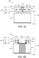
FIG. 4 (includingFIGs 4A-4D ), various views of a layout of aFET cell 400 are shown, in accordance with an embodiment of the present invention. More specifically,FIG. 4A shows a top view ofFET cell 400,FIG. 4B shows a partial top view ofFET cell 400 that depicts more clearly the features associated with the input bond pad and the connections to the gate fingers,FIG. 4C is a cross-sectional view of theFET cell 400 ofFIG. 4A throughline 4C-4C, andFIG. 4D is a cross-sectional view of theFET cell 400 ofFIG. 4A throughline 4D-4D. -
FET cell 400 may employ a multi-layer circuit approach configured to be disposed within asemiconductor substrate 402. As best shown inFIGs 4C and 4D , thesemiconductor substrate 402 includes abase semiconductor substrate 480 and a build-upstructure 490 coupled to the top surface of thebase semiconductor substrate 480. Thebase semiconductor substrate 480 may be formed, for example, from bulk or composite semiconductor materials (e.g., silicon (Si), gallium nitride (GaN), gallium arsenide (GaAs), silicon-on-insulator (Sol), GaN-on-insulator (e.g., GaN on Si, GaN on silicon carbide, GaN on sapphire, and so on), or other suitable materials). The build-upstructure 490 includes multiple dielectric layers that separate multiple patternedconductive layers FIGs 4C and 4D illustrate a build-upstructure 490 with four patterned conductive layers 492-495, other embodiments may include more or fewer conductive layers. In addition, although various features are illustrated within particular ones of the conductive layers 492-495, such features may be located in different layers than those depicted. In other words, inFIG. 4A , although the illustrated embodiment shows portions of below-describedsource bus 444 overlying portions of the below-described first and secondconductive structures gate bus 430, in alternate embodiments, the portions of the first and secondconductive structures gate bus 430 may instead overlie portions of thesource bus 444. -
FET cell 400 includes anactive region 404 formed insubstrate 402.Active region 404 is bounded by anouter periphery 406, generally represented by a dashed line box.Active region 404 includes sets of interdigitatedinput gate fingers output drain fingers common source fingers substrate 402 and oriented substantially parallel to one another. In alternate embodiments, a FET cell may include more or fewer gate fingers, drain fingers, and source fingers. For example, in some embodiments, a FET call may include as few as two gate fingers, one drain finger, and two source fingers (or two gate fingers, two drain fingers, and one source finger, if the locations of the source and drain regions are switched). - As most clearly shown in
FIG. 4B , in which various features fromFIG. 4A are removed for clarity, gate fingers 410-415 are coupled together by agate bus 430. A first bond pad, referred to herein as aninput bond pad 440, is coupled to thegate bus 430 at an input side ofactive region 404. Theinput bond pad 440 is positioned outside ofouter periphery 406 ofactive region 404 at a first longitudinal end of the interdigitated set of gate, drain and source fingers 410-415, 416-418, 420-423. - According to an embodiment, the
gate bus 430 includes a firstconductive structure 450 with a proximal end coupled to theinput bond pad 440 in afirst location 451, and a secondconductive structure 460 with a proximal end coupled to theinput bond pad 440 in asecond location 461 that is separated across a portion of theinput bond pad 440 from thefirst location 451. In order to readily distinguish the various structures in the various metal layers,gate bus 430 interconnecting gate fingers 410-415 to inputbond pad 440 are shaded with a stippled pattern. - In the illustrated embodiment, the first
conductive structure 450 includes a series-coupled arrangement ofconductive vias 452,conductive lines 453, and aconductive terminal 454 at a distal end of the firstconductive structure 450. Similarly, the secondconductive structure 460 includes a series-coupled arrangement ofconductive vias 462,conductive lines 463, and aconductive terminal 464 at a distal end of the secondconductive structure 460. As best visible inFIG. 4B , the first and secondconductive structures source TSV 446, which will be described later. As also best visible inFIG. 4B , anon-conductive gap 432 is present between theconductive terminals conductive terminals conductive structures non-conductive gap 432 is present between the distal ends of the first and secondconductive structures conductive structures non-conductive gap 432. - Proximal ends of a first set of the gate fingers 410-412 are directly electrically connected to the first
conductive structure 450, and proximal ends of a second set of the gate fingers 413-415 are directly electrically connected to the secondconductive structure 460. Accordingly, the firstconductive structure 450 provides a continuous first conductive path between the first set of gate fingers 410-412 and theinput bond pad 440, and the secondconductive structure 460 provides a continuous second conductive path between the second set of gate fingers 413-415 and theinput bond pad 440. AlthoughFIGs 4A and 4B show a first set of three gate fingers 410-412 coupled to the firstconductive structure 450, and a second set of three gate fingers 413-415 coupled to the secondconductive structure 460, in other embodiments, the first and second set of gate fingers may have fewer or more than three gate fingers, or otherwise may be differently defined. For example, in an alternate embodiment, the first set of gate fingers may include fewer fingers (e.g., only onefinger 410 or twofingers 410 and 411) and the second set of gate fingers may include more fingers (e.g., fingers 413-415plus finger 412 orfingers 412 and 411), or vice versa. As another example, the first set of gate fingers may include only a single first gate finger, and the second set of gate fingers may include only a single second gate finger. - According to an embodiment, an odd-mode oscillation stabilization circuit that includes a resistor 470 (
FIGs 4A ,4C ) is coupled across the distal ends of the first and secondconductive structures FIG. 4C , theresistor 470 may be an integrated resistor or a discrete resistor with afirst terminal 472 connected toterminal 454, and asecond terminal 474 connected toterminal 464. In embodiments in which theresistor 470 is an integrated resistor, theresistor 470 may be formed from a strip or body of resistive material (e.g., polysilicon or other suitable materials) that is integrally formed with thesemiconductor substrate 402. The body of resistive material may have a first end (or first terminal) connected to the terminal 454 and a second end (or second terminal) connected toterminal 464, with the resistance value being dependent upon the length, cross-sectional area, and electrical characteristics of the body of resistive material. Further, althoughFIG. 4C showsresistor 470 at the top surface of thesubstrate 402, the body of resistivematerial forming resistor 470 alternatively may be embedded in a layer that is below the top surface of thesubstrate 402. Alternatively, in embodiments in which theresistor 470 is a discrete resistor,terminals substrate 402, and theresistor 470 may include two conductive terminals that are connected to those bond pads. Either way, theresistor 470 may be considered to be connected acrossgap 432, or betweenterminals conductive structures gates 412 and 413), or between two sets of gate fingers (e.g., between a first set of gate fingers 410-412 and a second set of gate fingers 413-415). According to an embodiment, the resistance value ofresistor 470 is at least about 0.5 ohms, and may be as large as 5000 ohms or more. As more specific embodiments, the resistance value ofresistor 470 may be about 2 ohms, 50 ohms, 100 ohms, 1500 ohms, or some other value. The resistance value ofresistor 470 may be selected based on the total gate periphery on each side of theresistor 470, in some embodiments. As discussed above, the embodiment illustrated inFIGs 4A, 4B include three gate fingers 410-412 and 413-415 coupled to each ofconductive structures conductive structures resistor 470. - Referring again to
FIG. 4A , proximal ends of the drain fingers 416-418 are coupled together by adrain bus 419. A second bond pad, referred to herein as anoutput bond pad 442, is coupled to thedrain bus 419 at an output side ofactive region 404. Theoutput bond pad 442 is positioned outside ofouter periphery 406 ofactive region 404 at a second longitudinal end of the interdigitated set of gate, drain and source fingers 410-415, 416-418, 420-423. For enhanced understandability, drain fingers 416-418 anddrain bus 419, which interconnects drain fingers 416-418 tooutput bond pad 442, are shaded with upward and rightward directed cross-hatching. - Proximal ends of source fingers 420-423 are coupled to one another via a
source bus 444, and thesource bus 444, in turn, is coupled to asource TSV 446 disposed outside theouter periphery 406 ofactive region 404 proximateinput bond pad 440. Thesource TSV 446 more specifically is disposed between theactive area 404 and theinput bond pad 440, and also between the first and secondconductive structures source TSV 446 is surrounded (in the plane of the page forFIGs 4A and 4B ) by theinput bond pad 440, theactive area 404, and theconductive structures FET cell 400 thus represents an "end via" layout in whichsource TSV 446 is placed outside the bounding box (outer periphery 406) defined by theactive region 404. Accordingly, die size can be significantly reduced (as compared toFET cell 200 ofFIG. 2 ) by narrowing source fingers 420-423, because there are no via connections in the source fingers 420-423 ofFET cell 400. - As best shown in
FIG. 4D , thesource TSV 446 extends through base substrate 480 (i.e., between the top and bottom surfaces of the base substrate 480), and thus serves to electrically connect the source fingers 420-423 to a common node (e.g., aground plane 448 visible inFIGs 4C and 4C ) on a lower surface of thebase substrate 480. Thesource TSV 446 may have a noncircular cross-section (e.g., oval or trench-shaped), as shown inFIGs 4A and 4B , or may have a circular cross-section, in other embodiments. Again, for enhanced understandability, source fingers 420-423,source bus 444, andsource TSV 446, are shaded with downward and rightward directed cross-hatching. - In order to build a power transistor of a desired power capability, multiple instances of
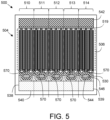
FET cell 400 may be replicated in parallel and interconnected with common input and output bond pads. For example,FIG. 5 shows a top view of aFET 500 that includes a number, N, of instances of theFET cell 400 ofFIG. 4 . More particularly,FET 500 includes fiveFET cells FET 500. - As previously discussed, semiconductor substrate 502 may include a base semiconductor substrate (e.g.,
base semiconductor substrate 480,FIGs 4C, 4D ) and a build-up structure (e.g., build-upstructure 490,FIGs 4C, 4D ) coupled to the top surface of the base semiconductor substrate. The base semiconductor substrate may be formed, for example, from bulk or composite semiconductor materials (e.g., Si, GaN, GaAs, Sol, GaN-on-insulator, or other suitable materials). The build-up structure includes multiple dielectric layers that separate multiple patterned conductive layers, along with conductive vias that electrically connect portions of the conductive layers. The various details and embodiments associated with substrate 402 (FIG. 4 ), discussed above, apply also to the substrate 502 ofFIG. 5 , and accordingly those details and embodiments are intended to apply also toFET 500. - Each of the FET cells 510-514 includes an active region (e.g.,
active region 404,FIG. 4A ) formed in the substrate 502. A combination of the active regions for all FET cells 510-514 is referred to as a cumulativeactive region 504, which is bounded by anouter periphery 506, generally represented by a dashed line box. Cumulativeactive region 504 includes all of the sets of interdigitated input gate fingers (e.g., gate fingers 410-415,FIGs 4A, 4B ), output drain fingers (e.g., drain fingers 416-418,FIG. 4A ), and common source fingers (e.g., source fingers 420-423,FIG. 4A ) for all of the FET cells 510-514, and the gate, drain, and source fingers all are oriented substantially parallel to one another. - Proximal ends of the drain fingers for all of the FET cells 510-514 are coupled together by a
drain bus 519. Anoutput bond pad 542 is coupled to thedrain bus 519 at an output side ofactive region 504. As shown inFIG. 5 , thedrain bus 519 and theoutput bond pad 542 are elongated conductive structures that extend across the combined width of all of the FET cells 510-514. WhenFET 500 is incorporated into a larger electrical system (e.g., an amplifier), a plurality of wirebonds would have first ends coupled along the length of theoutput bond pad 542, and second ends coupled to a bond pad on a substrate that supports other portions of the electrical system. - Additionally, proximal ends of the source fingers for each of the FET cells 510-514 are coupled to one another via a
source bus 544 associated with each FET cell 510-514, and eachsource bus 544, in turn, is coupled to asource TSV 546 disposed outside theouter periphery 506 of active region 504 (i.e., at a location between theactive region 504 and theinput bond pad 540, discussed below). According to an embodiment, the N source busses 544 for the N FET cells 510-514 may be electrically coupled together, as shown inFIG. 5 . - According to an embodiment, the gate fingers (e.g., gate fingers 410-415,
FIGs 4A, 4B ) for each FET cell 510-514 are coupled together by agate bus 530 associated with each FET cell 510-514. Aninput bond pad 540, is coupled to all of the gate busses 530 at an input side ofactive region 504. As shown inFIG. 5 , theinput bond pad 540 is an elongated conductive structure that extends across the combined width of all of the FET cells 510-514. More specifically, theinput bond pad 540 is formed in the semiconductor substrate 502 and spaced apart from theactive area 504, and theinput bond pad 540 is physically and electrically continuous between first and second ends 538, 539 of the input bond pad 540 (i.e., theinput bond pad 540 is unsegmented). WhenFET 500 is incorporated into a larger electrical system (e.g., an amplifier), a plurality of wirebonds would have first ends coupled along the length of theinput bond pad 540, and second ends coupled to a bond pad on a substrate that supports other portions of the electrical system. - According to an embodiment, each
gate bus 530 includes a first conductive structure (e.g.,conductive structure 450,FIGs 4A, 4B ) with a proximal end coupled to theinput bond pad 540 in a first location, and a second conductive structure (e.g.,conductive structure 460,FIGs 4A, 4B ) with a proximal end coupled to theinput bond pad 540 in a second location that is separated across a portion of theinput bond pad 540 from the first location. - As discussed above in conjunction with
FIG. 4 , each of the first and second conductive structures of eachgate bus 530 includes a series-coupled arrangement of conductive vias, conductive lines, and a conductive terminal (e.g.,terminals FIG. 4B ) at a distal end of the first and second conductive structures, and a non-conductive gap (e.g.,gap 432,FIG. 4B ) is present between the conductive terminals of eachgate bus 530. Proximal ends of a first set of the gate fingers (e.g., fingers 410-412,FIG. 4B ) are directly electrically connected to the first conductive structure, and proximal ends of a second set of the gate fingers (e.g., fingers 413-415,FIG. 4B ) are directly electrically connected to the second conductive structure. As can be seen inFIG. 5 , the first and second conductive structures of adjacent FET cells (e.g.,cells 510 and 511) may be formed from abutting portions of a single conductive feature. - According to an embodiment, an odd-mode oscillation stabilization circuit that includes multiple resistors 570 (e.g., multiple instances of
resistor 470,FIGs 4A ,4C ) is coupled to the FET cells 510-514. More specifically, within each FET cell 510-514, aresistor 570 is coupled across the distal ends of the first and second conductive structures of that FET cell 510-514. More specifically, and as best shown inFIG. 4C , eachresistor 570 may be an integrated or a discrete resistor with a first terminal (e.g., terminal 472,FIG. 4C ) connected to one of the gate bus terminals (e.g., terminal 454,FIGs 4B ,4C ), and a second terminal (e.g., terminal 474,FIG. 4C ) connected to the other one of the gate bus terminals (e.g., terminal 464,FIGs 4B ,4C ). In embodiments in which theresistors 570 are integrated resistors, theresistors 570 may be formed from resistive material (e.g., polysilicon or other suitable materials) that are integrally formed with the semiconductor substrate 502. Alternatively, in embodiments in which theresistors 570 are discrete resistors, the gate bus terminals may include bond pads exposed at the top surface of theFET 500, and theresistors 570 may be connected to those bond pads. - Referring both to
FIGs 4 and5 , the odd-mode oscillation stabilization circuits ofFET cell 400 andFET 500 comprisesresistors FET 500, also the conductive features that electrically interconnect those resistors 570 (e.g., portions of the first and second conductive structures of the gate busses 530 thatinterconnect resistors 570 across the width of the FET 500). Theresistors FET cell 400 or theFET 500, while having little or no impact on the intended signal for amplification. - Because the lateral resistance required for odd-mode stabilization is included within the
FET cells 400, 510-514, no additional resistors need to be added to an array of FET cells (e.g., FET cells 510-514), and accordingly the odd-mode stabilization may be achieved without segmenting theinput bond pad FET 500, theinput bond pad 540 extends continuously along the combined width of the plurality of FET cells 510-514, and thus theinput bond pad 540 may be described as an "unsegmented" or "physically and electrically continuous" bond pad. According to an embodiment, thebond pad 540 is formed from a single continuous portion of a single conductive layer. Essentially, the above-described embodiments provide very robust stability against odd-mode oscillations, without requiring bond pad segmentation. - In addition, by positioning the
source TSVs input bond pad active area structures FIG. 4B ) of the gate busses 430, 530 are constrained to have a minimum physical/electrical length between theinput bond pad FIGs 4A, 4B ), with a corresponding associated inductance. For example, the inductance of each of the gate busses 430, 530 may be in a range of about 10 picohenries (pH) to about 200 pH, in some embodiments, or about 45 pH to about 75pH in other embodiments, although the inductance could be smaller or larger than these ranges, as well. Even though thelateral resistor gate fingers FIGs 4A, 4B ) is shorted out by theinput bond pad lateral resistor input bond pad input bond pad structures FIG. 4B ) that run on both sides of the source TSV (e.g.,TSV FIGs 4A ,5 ), every gate finger has a connection path back to the input bond pad that does not go through the stabilizingresistor - Embodiments of
FET 500 may be incorporated into power amplifiers or other circuitry. As one specific example,FIG. 6 illustrates apower amplifier module 600 that includes aDoherty amplifier 610 implemented on a module substrate.Doherty amplifier 610 includes anRF input node 612, anRF output node 614, apower splitter 620, acarrier amplifier path 630 with one or more carrier amplifier dies, a peakingamplifier path 650 with one or more peaking amplifier dies, a phase delay andimpedance inversion element 670, and a combiningnode 672. - When incorporated into a larger RF system, the
RF input node 612 is coupled to an RF signal source, and theRF output node 614 is coupled to a load 690 (e.g., an antenna or other load). The RF signal source provides an input RF signal, which is an analog signal that includes spectral energy that typically is centered around one or more carrier frequencies. Fundamentally, theDoherty amplifier 610 is configured to amplify the input RF signal, and to produce an amplified RF signal at theRF output node 614. - The
power splitter 620 has aninput 622 and twooutputs power splitter input 622 is coupled to theRF input node 612 to receive the input RF signal. Thepower splitter 620 is configured to divide the RF input signal received atinput 622 into first and second RF signals (or carrier and peaking signals), which are provided to the carrier and peakingamplifier paths outputs power splitter 620 includes a first phase shift element, which is configured to impart a first phase shift (e.g., about a 90 degree phase shift) to the peaking signal before it is provided tooutput 626. Accordingly, atoutputs - The
outputs power splitter 620 are connected to the carrier and peakingamplifier paths carrier amplifier path 630 is configured to amplify the carrier signal from thepower splitter 620, and to provide the amplified carrier signal to thepower combining node 672. Similarly, the peakingamplifier path 650 is configured to amplify the peaking signal from thepower splitter 620, and to provide the amplified peaking signal to thepower combining node 672, where thepaths power combining node 672. - According to an embodiment, the
carrier amplifier path 630 includes an input circuit 631 (e.g., including an impedance matching circuit), acarrier amplifier 632 implemented using one or more carrier amplifier dies (e.g., one or more instances ofFET 500,FIG. 5 ), and a phase shift andimpedance inversion element 670. - The
carrier amplifier 632 includes anRF input terminal 634, anRF output terminal 638, and one or more amplification stages coupled between the input andoutput terminals RF input terminal 634 is coupled throughinput circuit 631 to thefirst output 624 of thepower splitter 620, and thus theRF input terminal 634 receives the carrier signal produced by thepower splitter 620. - Each amplification stage of the
carrier amplifier 632 includes a power transistor. In a single-stage carrier amplifier 632, a single power transistor may be implemented on a single power amplifier die. In a two-stage carrier amplifier 632, two power transistors may be implemented on a single power amplifier die, or each power amplifier may be implemented on a separate die. - Either way, each power transistor includes a control terminal and first and second current-carrying terminals (e.g., a drain terminal and a source terminal). In a single-stage device, which would include a single power transistor, the control terminal is electrically connected to the
RF input terminal 634, one of the current-carrying terminals (e.g., the drain terminal) is electrically connected to theRF output terminal 638, and the other current-carrying terminal (e.g., the source terminal) is electrically connected to a ground reference (or another voltage reference). Conversely, a two-stage amplifier would include two power transistors coupled in series, where a first transistor functions as a driver amplifier transistor that has a relatively low gain, and a second transistor functions as a final-stage amplifier transistor that has a relatively high gain. - The
RF output terminal 638 of thecarrier amplifier 632 is coupled to thepower combining node 672 through phase shift andimpedance inversion element 670, in an embodiment. According to an embodiment, the impedance inversion element is a lambda/4 (λ/4) transmission line phase shift element (e.g., a microstrip line), which imparts about a 90 degree relative phase shift to the carrier signal after amplification by thecarrier amplifier 632. A first end of theimpedance inversion element 670 is coupled to theRF output terminal 638 of thecarrier amplifier 632, and a second end of thephase shift element 670 is coupled to thepower combining node 672. - Reference is now made to the peaking
amplifier path 650, which includes a peakingamplifier 652 and an input circuit 651 (e.g., including an impedance matching circuit), in an embodiment. The peakingamplifier 652 includes anRF input terminal 654, anRF output terminal 658, and one or more amplification stages coupled between the input andoutput terminals RF input terminal 654 is coupled to thesecond output 626 of thepower splitter 620, and thus theRF input terminal 654 receives the peaking signal produced by thepower splitter 620. - As with the
carrier amplifier 632, each amplification stage of the peakingamplifier 652 includes a power transistor with a control terminal and first and second current-carrying terminals. The power transistor(s) of the peakingamplifier 652 may be electrically coupled between the RF input andoutput terminals carrier amplifier 632. Additional other details discussed with in conjunction with the description of thecarrier amplifier 632 also apply to the peakingamplifier 652, and those additional details are not reiterated here for brevity. - The
RF output terminal 658 of the peakingamplifier 652 is coupled to thepower combining node 672. According to an embodiment, theRF output terminal 658 of the peakingamplifier 652 and the combiningnode 672 are implemented with a common element. More specifically, in an embodiment, theRF output terminal 658 of the peakingamplifier 652 is configured to function both as the combiningnode 672 and as theoutput terminal 658 of the peakingamplifier 652. To facilitate combination of the amplified carrier and peaking signals, and as mentioned above, the RF output terminal 658 (and thus the combining node 672) is connected to the second end of the phase shift andimpedance inversion element 670. In other embodiments, the combiningnode 672 may be a separate element from theRF output terminal 658. - Either way, the amplified carrier and peaking RF signals combine in phase at the combining
node 672. The combiningnode 672 is electrically coupled to theRF output node 614 to provide the amplified and combined RF output signal to theRF output node 614. In an embodiment, an outputimpedance matching network 674 between the combiningnode 672 and theRF output node 614 functions to present proper load impedances to each of the carrier and peakingamplifier RF output node 614, to which an output load 690 (e.g., an antenna) is connected. -
Amplifier 610 is configured so that thecarrier amplifier path 630 provides amplification for relatively low level input signals, and bothamplification paths carrier amplifier 632 so that thecarrier amplifier 632 operates in a class AB mode, and biasing the peakingamplifier 652 so that the peakingamplifier 652 operates in a class C mode. - An example of a physical implementation of the Doherty amplifier circuit of
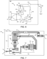
FIG. 6 now will be described in detail in conjunction withFIG. 7 . More specifically,FIG. 7 shows a top view of aDoherty amplifier module 700, in accordance with an example configuration of the present invention. -
Doherty amplifier module 700 includes asubstrate 702, a power splitter 720 (e.g.,power splitter 620,FIG. 6 ), driver-stage and final-stage carrier amplifier dies 733, 734 (e.g., corresponding tocarrier amplifier 632,FIG. 6 ), driver-stage and final-stage peaking amplifier dies 753, 754 (e.g., corresponding to peakingamplifier 652,FIG. 6 ), a phase shift and impedance inversion element 770 (e.g., phase shift andimpedance inversion element 670,FIG. 6 ), and various other circuit elements, which will be discussed in more detail below. Each of the dies 733, 734, 753, 754 may be mounted over a heat dissipation structure (e.g., a conductive coin or thermal vias) that extends through thesubstrate 702, and which enables heat produced by the dies 733, 734, 753, 754 during operation to be transferred though thesubstrate 702 to a system-level heat dissipation structure. -
Doherty amplifier module 700 may be implemented as a land grid array (LGA) module, for example. Accordingly,substrate 702 has acomponent mounting surface 704 and a land surface (not shown) oppositecomponent mounting surface 704.Component mounting surface 704 and the components mounted to thatsurface 704 optionally may be covered with an encapsulant material (not shown). Alternatively, the components could be contained within an air cavity, which is defined by various structures (not illustrated) overlying mountingsurface 704. - A conductive landing pad 711 (represented by a dashed line box) exposed at the land surface is electrically coupled through
substrate 702 to aconductive contact 712 at the mountingsurface 704.Landing pad 711 and contact 712, along with the electrical connections between them, function as the RF input node (e.g.,RF input node 612,FIG. 6 ) formodule 700. Similarly, another conductive landing pad 713 (represented by a dashed line box) exposed at the land surface is electrically coupled throughsubstrate 702 to anotherconductive contact 714 at the mountingsurface 704.Landing pad 713 and contact 714, along with the electrical connections between them, function as the RF output node (e.g.,RF output node 614,FIG. 6 ) formodule 700. -
Power splitter 720 is coupled to mountingsurface 704, and may include one or more discrete die and/or components, although it is represented inFIG. 7 as a single element.Power splitter 720 includes an input terminal 722 (e.g.,input 622,FIG. 6 ) and two output terminals, not numbered (e.g., outputs 624, 626,FIG. 6 ).Input terminal 722 is electrically coupled (e.g., through wirebonds, as shown) toconductive contact 712 to receive an input RF signal. In addition, the output terminals ofpower splitter 720 are electrically coupled (e.g., through additional wirebonds, as shown) to conductive traces, not numbered, at the mountingsurface 704.Power splitter 720 is configured to split the power of the input RF signal received throughinput terminal 722 into first and second RF signals (e.g., carrier and peaking signals), which are produced at the output terminals of thepower splitter 720. In addition,power splitter 720 may include one or more phase shift elements configured to impart about a 90 degree phase shift to the RF signal provided at one of the output terminals of thepower splitter 720.Power splitter 720 may consist of a single surface-mount component, or may consist of multiple fixed-value, passive components. - The first RF signal produced by the
power splitter 720 is amplified through a carrier amplifier path. The carrier amplifier path includes an input circuit 731 (e.g.,input circuit 631,FIG. 6 ), acarrier amplifier 732, and a phase shift and impedance inversion element 770 (e.g.,impedance inversion element 670,FIG. 6 ). -
Input circuit 731 is configured to provide proper impedance matching between the first output ofpower splitter 720 and the input to thecarrier amplifier 732. The illustrated embodiment ofcarrier amplifier 732 embodies a two-stage amplifier. More specifically, thecarrier amplifier 732 includes a driver-stage carrier amplifier die 733 coupled in series to a final-stage carrier amplifier die 734. Driver-stage carrier amplifier die 733 includes a first power transistor 736 (e.g., an instance of an embodiment ofFET 500,FIG. 5 ), which is configured to apply a relatively low gain to the carrier signal. Final-stage carrier amplifier die 734 includes a second power transistor 737 (e.g., another instance of an embodiment ofFET 500,FIG. 5 ), which is configured to apply a relatively high gain to the carrier signal after preliminary amplification by the driver-stage carrier amplifier die 733. Although not shown inFIG. 7 , an impedance matching circuit may be implemented between the first andsecond power transistors power transistors carrier amplifier 732 may embody a single stage amplifier (i.e., including only one carrier amplifier die), or may include more than two amplification stages. - An amplified RF carrier signal is produced by the final-stage carrier amplifier die 734 at
output terminal 738. In the illustrated example, theRF output terminal 738 is electrically coupled to a first end of phase shift andimpedance inversion element 770 with a plurality of parallel, closely spaced wirebonds. Phase shift andimpedance inversion element 770 may be implemented with a transmission line (e.g., a microstrip line) having an electrical length of about lambda/4 (λ/4) or less. The transmission line has a first end that is proximate to the final-stage carrier amplifier die 734 and a second end that is proximate to the final-stage peaking amplifier die 754, discussed below. - Moving back to
power splitter 720, the second RF signal produced by thepower splitter 720 is amplified through a peaking amplifier path. The peaking amplifier path includes an input circuit 751 (e.g.,input circuit 651,FIG. 6 ), and a peakingamplifier 752. -
Input circuit 751 is configured to provide proper impedance matching between the second output ofpower splitter 720 and the input to the peakingamplifier 752. The illustrated embodiment of peakingamplifier 752 embodies a two-stage amplifier. More specifically, the peakingamplifier 752 includes a driver-stage peaking amplifier die 753 coupled in series to a final-stage peaking amplifier die 754. Driver-stage peaking amplifier die 753 includes a third power transistor 756 (e.g., another instance of an embodiment ofFET 500,FIG. 5 ), which is configured to apply a relatively low gain to the peaking signal. Final-stage peaking amplifier die 754 includes a fourth power transistor 757 (e.g., another instance of an embodiment ofFET 500,FIG. 5 ), which is configured to apply a relatively high gain to the peaking signal after preliminary amplification by the driver-stage peaking amplifier die 753. Although not shown inFIG. 7 , an impedance matching circuit may be implemented between the third andfourth power transistors power transistors amplifier 752 may embody a single stage amplifier (i.e., including only one peaking amplifier die), or may include more than two amplification stages. - An amplified RF peaking signal is produced by the final-stage peaking amplifier die 754 at
RF output terminal 758.RF output terminal 758 also functions as a combining node 772 (e.g., combiningnode 672,FIG. 6 ) at which the amplified and delayed carrier amplifier signal is combined, in phase, with an amplified peaking amplifier signal. To receive the amplified and delayed carrier amplifier signal, RF output terminal 758 (and thus combining node 672) is electrically coupled to a second end of theimpedance inversion element 770 with a wirebond array. More specifically, the amplified carrier signal produced by thecarrier amplifier 732 and the amplified peaking signal produced by the peakingamplifier 752 are received at the combiningnode 772, where they combine in phase. - RF output terminal 758 (and combining node 772) is electrically coupled to a
conductive output trace 773 with a wirebond array. An output impedance matching network 774 (e.g., matchingnetwork 674,FIG. 6 ) is implemented alongoutput trace 773. In addition, adecoupling capacitor 780 may be coupled alongoutput trace 773. Outputimpedance matching network 774 functions to present the proper load impedance to combiningnode 772. Although the detail is not shown inFIG. 7 , the outputimpedance matching network 774 may include various discrete and/or integrated components (e.g., capacitors, inductors, and/or resistors) to provide the desired impedance matching. Outputimpedance matching network 774 is electrically coupled to aconductive contact 714 at mountingsurface 704.Conductive contact 714 is in electrical contact with alanding pad 713 exposed at the land surface ofsubstrate 702.Landing pad 713 and contact 714, along with the electrical connections between them, function as the RF output node (e.g.,RF output node 614,FIG. 6 ) formodule 700. - As indicated above, each of the
transistors FET 500,FIG. 5 ), which includes an odd-mode oscillation stabilization circuit as described above. In various alternate embodiments, only some (but not all) of thetransistors FET 500,FIG. 5 ) may be used where die size is not constrained primarily by thermal requirements (e.g., in peaking amplifier 754), whereas differently configured FETs may be used elsewhere (e.g., in carrier amplifier die 734). - The above described embodiment includes two-way Doherty power amplifier implementation, which includes a carrier amplifier and a peaking amplifier. According to other embodiments, a Doherty power amplifier may include more than one peaking amplifier, or
module 700 may be modified to implement types of amplifiers other than Doherty amplifiers. That is, various modifications may be made tomodule 700 while still including transistors that have an odd-mode oscillation stabilization circuit as described in detail above. - Further, although embodiments have been described herein with respect to a Doherty power amplifier, those of skill in the art would understand, based on the description herein, that embodiments of the inventive subject matter may be used in conjunction with virtually any type of single- or multiple-path amplifier. Accordingly, the transistor embodiments having the odd-mode oscillation stabilization circuits described herein are not limited to use with Doherty amplifiers, nor are the transistor embodiments having odd-mode oscillation stabilization circuits limited to use with amplifiers having only two amplification paths. Rather, the transistor embodiments having the odd-mode oscillation stabilization circuit may be implemented within a wide variety of circuits.
- A transistor includes first and second sets of gate fingers formed in an active area of a semiconductor substrate, an input bond pad formed in the semiconductor substrate and spaced apart from the active area, a first conductive structure with a proximal end coupled to the input bond pad and a distal end coupled to the first set of gate fingers, and a second conductive structure with a proximal end coupled to the input bond pad and a distal end coupled to the second set of gate fingers. A non-conductive gap is present between the distal ends of the first and second conductive structures. The transistor further includes an odd-mode oscillation stabilization circuit that includes a first resistor with a first terminal coupled to the distal end of the first conductive structure, and a second terminal coupled to the distal end of the second conductive structure.
- In a first aspect, a transistor includes first and second sets of gate fingers formed in an active area of a semiconductor substrate, an input bond pad formed in the semiconductor substrate and spaced apart from the active area, a first conductive structure with a proximal end coupled to the input bond pad and a distal end coupled to the first set of gate fingers, and a second conductive structure with a proximal end coupled to the input bond pad and a distal end coupled to the second set of gate fingers. A non-conductive gap is present between the distal ends of the first and second conductive structures. The transistor further includes an odd-mode oscillation stabilization circuit that includes a first resistor with a first terminal coupled to the distal end of the first conductive structure, and a second terminal coupled to the distal end of the second conductive structure.
- In a second aspect a transistor includes a semiconductor substrate with an active area, and an input bond pad formed in the semiconductor substrate and spaced apart from the active area. The input bond pad is physically and electrically continuous between first and second ends of the input bond pad. The transistor further includes first and second transistor cells. The first transistor cell includes a first set of gate fingers and a second set of gate fingers formed in the active area, a first conductive structure with a proximal end coupled to the input bond pad between the first and second ends and a distal end coupled to the first set of gate fingers, and a second conductive structure with a proximal end coupled to the input bond pad between the first and second ends and a distal end coupled to the second set of gate fingers. A first non-conductive gap is present between the distal ends of the first and second conductive structures. The second transistor cell includes a third set of gate fingers and a fourth set of gate fingers formed in the active area, a third conductive structure with a proximal end coupled to the input bond pad between the first and second ends and a distal end coupled to the third set of gate fingers, and a fourth conductive structure with a proximal end coupled to the input bond pad between the first and second ends and a distal end coupled to the fourth set of gate fingers. A second non-conductive gap is present between the distal ends of the third and fourth conductive structures. The transistor further includes an odd-mode oscillation stabilization circuit that includes a first resistor and a second resistor. The first resistor is coupled across the first gap to the distal ends of the first and second conductive structures, and the second resistor is coupled across the second gap to the distal ends of the third and fourth conductive structures.
- In one or more embodiments, the transistor may further comprise: a first through substrate via disposed in the semiconductor substrate between the active area and the input bond pad, wherein the first and second conductive structures are located on opposite sides of the first through substrate via; and a second through substrate via disposed in the semiconductor substrate between the active area and the input bond pad, wherein the third and fourth conductive structures are located on opposite sides of the second through substrate via.
- In one or more embodiments, the transistor may further comprise: a first source finger formed in the active area, wherein the first source finger is electrically coupled to the first through substrate via; a second source finger formed in the active area, wherein the second source finger is electrically coupled to the second through substrate via; and a conductive layer on a bottom surface of the semiconductor substrate, wherein the first and second through substrate vias electrically connect the first and second source fingers and the conductive layer.
- In one or more embodiments, the first conductive structure may include a first terminal at the distal end of the first conductive structure; the second conductive structure includes a second terminal at the distal end of the second conductive structure; the third conductive structure includes a third terminal at the distal end of the third conductive structure; the fourth conductive structure includes a fourth terminal at the distal end of the fourth conductive structure; the first resistor is connected to the first and second terminals; and the second resistor is connected to the third and fourth terminals.
- In one or more embodiments, the first, second, third, and fourth conductive structures each may be characterized by an inductance, and wherein during operation of the transistor, the first and second resistors are not shorted out by the input bond pad at frequencies at which odd-mode oscillations occur.
- In one or more embodiments, the proximal end of the first conductive structure may be coupled to the input bond pad in a first location; the proximal end of the second conductive structure is coupled to the input bond pad in a second location that is separated across a portion of the input bond pad from the first location; the proximal end of the third conductive structure is coupled to the input bond pad in a third location; and the proximal end of the fourth conductive structure is coupled to the input bond pad in a fourth location that is separated across a portion of the input bond pad from the third location.
- In one or more embodiments, the first set of gate fingers may include multiple first gate fingers; and the second set of gate fingers may include multiple second gate fingers.
- In one or more embodiments, the first set of gate fingers may include a single first gate finger; and the second set of gate fingers may include a single second gate finger.
- This disclosure is intended to explain how to fashion and use various embodiments in accordance with the invention rather than to limit the true, intended, and fair scope and spirit thereof. The foregoing description is not intended to be exhaustive or to limit the invention to the precise form disclosed. Modifications or variations are possible in light of the above teachings. The embodiment(s) was chosen and described to provide the best illustration of the principles of the invention and its practical application, and to enable one of ordinary skill in the art to utilize the invention in various embodiments and with various modifications as are suited to the particular use contemplated. All such modifications and variations are within the scope of the invention as determined by the appended claims, as may be amended during the pendency of this application for patent, and all equivalents thereof, when interpreted in accordance with the breadth to which they are fairly, legally, and equitably entitled.
Claims (10)
- A transistor comprising:a semiconductor substrate;a first set of gate fingers and a second set of gate fingers formed in an active area of the semiconductor substrate;an input bond pad formed in the semiconductor substrate and spaced apart from the active area;a first conductive structure with a proximal end coupled to the input bond pad and a distal end coupled to the first set of gate fingers;a second conductive structure with a proximal end coupled to the input bond pad and a distal end coupled to the second set of gate fingers, wherein a non-conductive gap is present between the distal ends of the first and second conductive structures; andan odd-mode oscillation stabilization circuit that includes a first resistor with first and second terminals, wherein the first terminal is coupled to the first set of gate fingers at the distal end of the first conductive structure, and the second terminal is coupled to the second set of gate fingers at the distal end of the second conductive structure.
- The transistor of claim 1, further comprising:
a through substrate via disposed in the semiconductor substrate between the active area and the input bond pad, wherein the first and second conductive structures are located on opposite sides of the through substrate via. - The transistor of claim 2, further comprising:a source finger formed in the active area, wherein the source finger is electrically coupled to the through substrate via; anda conductive layer on a bottom surface of the semiconductor substrate, wherein the through substrate via electrically connects the source finger and the conductive layer.
- The transistor of any preceding claim, wherein:the first conductive structure includes a first bond pad at the distal end of the first conductive structure;the second conductive structure includes a second bond pad at the distal end of the second conductive structure; andthe first resistor is a surface mount component coupled to the first and second bond pads.
- The transistor of any preceding claim, wherein:the first conductive structure includes a first terminal at the distal end of the first conductive structure;the second conductive structure includes a second terminal at the distal end of the second conductive structure; andthe first resistor is integrally formed with the semiconductor substrate and includes a body of resistive material with a first end connected to the first terminal, and a second end connected to the second terminal.
- The transistor of any preceding claim, wherein the first and second conductive structures each are characterized by an inductance, and wherein during operation of the transistor, the first resistor is not shorted out by the input bond pad at frequencies at which odd-mode oscillations occur.
- The transistor of any preceding claim, wherein:the proximal end of the first conductive structure is coupled to the input bond pad in a first location; andthe proximal end of the second conductive structure is coupled to the input bond pad in a second location that is separated across a portion of the input bond pad from the first location.
- The transistor of any preceding claim, wherein:the first set of gate fingers includes multiple first gate fingers; andthe second set of gate fingers includes multiple second gate fingers.
- The transistor of any of claims 1 to 7, wherein:the first set of gate fingers includes a single first gate finger; andthe second set of gate fingers includes a single second gate finger.
- The transistor of any preceding claim, further comprisinga third set of gate fingers and a fourth set of gate fingers formed in the active area of the semiconductor substrate;a third conductive structure with a proximal end coupled to the input bond pad and a distal end coupled to the third set of gate fingers; anda fourth conductive structure with a proximal end coupled to the input bond pad and a distal end coupled to the fourth set of gate fingers, andwherein the odd-mode oscillation stabilization circuit further includes a second resistor with first and second terminals, wherein the first terminal of the second resistor is coupled to the third set of gate fingers at the distal end of the third conductive structure, and the second terminal of the second resistor is coupled to the fourth set of gate fingers at the distal end of the fourth conductive structure, andwherein the input bond pad is physically and electrically continuous between the proximal ends of the first, second, third, and fourth conductive structures.
Applications Claiming Priority (1)
| Application Number | Priority Date | Filing Date | Title |
|---|---|---|---|
| US17/456,434 US11842996B2 (en) | 2021-11-24 | 2021-11-24 | Transistor with odd-mode oscillation stabilization circuit |
Publications (2)
| Publication Number | Publication Date |
|---|---|
| EP4195260A2 true EP4195260A2 (en) | 2023-06-14 |
| EP4195260A3 EP4195260A3 (en) | 2023-07-19 |
Family
ID=84044338
Family Applications (1)
| Application Number | Title | Priority Date | Filing Date |
|---|---|---|---|
| EP22204791.2A Pending EP4195260A3 (en) | 2021-11-24 | 2022-10-31 | Transistor with odd-mode oscillation stabilization circuit |
Country Status (3)
| Country | Link |
|---|---|
| US (1) | US11842996B2 (en) |
| EP (1) | EP4195260A3 (en) |
| CN (1) | CN116169135A (en) |
Family Cites Families (20)
| Publication number | Priority date | Publication date | Assignee | Title |
|---|---|---|---|---|
| JP3515886B2 (en) | 1997-09-29 | 2004-04-05 | 三菱電機株式会社 | Semiconductor device and manufacturing method thereof |
| US7688152B2 (en) * | 2006-07-10 | 2010-03-30 | Triquint Semiconductor, Inc | High frequency stabilization network for microwave devices and monolithic integrated circuits |
| US8431973B2 (en) * | 2008-12-10 | 2013-04-30 | Kabushiki Kaisha Toshiba | High frequency semiconductor device |
| US8008977B2 (en) * | 2009-04-14 | 2011-08-30 | Triquint Semiconductor, Inc. | Field-plated transistor including feedback resistor |
| JP5526221B2 (en) * | 2010-03-09 | 2014-06-18 | パナソニック株式会社 | Semiconductor device |
| JP5361951B2 (en) * | 2011-06-17 | 2013-12-04 | 株式会社東芝 | Semiconductor power amplifier |
| JP5983117B2 (en) * | 2012-07-11 | 2016-08-31 | 三菱電機株式会社 | Semiconductor device |
| JP5711778B2 (en) * | 2013-03-06 | 2015-05-07 | 株式会社東芝 | Semiconductor device |
| JP2014175368A (en) * | 2013-03-06 | 2014-09-22 | Toshiba Corp | Field effect transistor and semiconductor device |
| GB201323159D0 (en) | 2013-12-31 | 2014-02-12 | Diamond Microwave Devices Ltd | Improved matching techniques for wide-bandgap power transistors |
| US10128365B2 (en) * | 2016-03-17 | 2018-11-13 | Cree, Inc. | Bypassed gate transistors having improved stability |
| US9947616B2 (en) * | 2016-03-17 | 2018-04-17 | Cree, Inc. | High power MMIC devices having bypassed gate transistors |
| DE102017110536B4 (en) * | 2017-05-15 | 2022-06-30 | Infineon Technologies Ag | Wide band gap semiconductor device including gate fingers between bond pads and semiconductor module |
| US10545055B2 (en) * | 2017-06-13 | 2020-01-28 | Semiconductor Components Industries, Llc | Electronic device including a temperature sensor |
| US10268789B1 (en) * | 2017-10-03 | 2019-04-23 | Cree, Inc. | Transistor amplifiers having node splitting for loop stability and related methods |
| US10600746B2 (en) * | 2018-07-19 | 2020-03-24 | Cree, Inc. | Radio frequency transistor amplifiers and other multi-cell transistors having gaps and/or isolation structures between groups of unit cell transistors |
| US10629526B1 (en) | 2018-10-11 | 2020-04-21 | Nxp Usa, Inc. | Transistor with non-circular via connections in two orientations |
| US11417746B2 (en) * | 2019-04-24 | 2022-08-16 | Wolfspeed, Inc. | High power transistor with interior-fed fingers |
| EP4333304A2 (en) * | 2019-10-31 | 2024-03-06 | Infineon Technologies Austria AG | Semiconductor device and inverter |
| US11670605B2 (en) * | 2020-04-03 | 2023-06-06 | Wolfspeed, Inc. | RF amplifier devices including interconnect structures and methods of manufacturing |
-
2021
- 2021-11-24 US US17/456,434 patent/US11842996B2/en active Active
-
2022
- 2022-09-28 CN CN202211188240.XA patent/CN116169135A/en active Pending
- 2022-10-31 EP EP22204791.2A patent/EP4195260A3/en active Pending
Also Published As
| Publication number | Publication date |
|---|---|
| CN116169135A (en) | 2023-05-26 |
| US20230163121A1 (en) | 2023-05-25 |
| EP4195260A3 (en) | 2023-07-19 |
| US11842996B2 (en) | 2023-12-12 |
Similar Documents
| Publication | Publication Date | Title |
|---|---|---|
| US10879168B2 (en) | Transistor with non-circular via connections in two orientations | |
| EP3331161B1 (en) | Amplifier die with elongated side pads, and amplifier modules that incorporate such amplifier die | |
| EP3337037B1 (en) | Doherty amplifiers and amplifier modules with shunt inductance circuits that affect transmission line length between carrier and peaking amplifier outputs | |
| EP2458730B1 (en) | Radiofrequency amplifier | |
| US10593619B1 (en) | Transistor shield structure, packaged device, and method of manufacture | |
| US10594266B2 (en) | Multiple-path amplifier with series component along inverter between amplifier outputs | |
| EP1573813B1 (en) | Rf power transistor with internal bias feed | |
| US10381984B2 (en) | Amplifiers and amplifier modules with shunt inductance circuits that include high-Q capacitors | |
| EP2242103B1 (en) | Chip with field-effect transistors and contact bumps for flip-chip connection | |
| EP3771094A2 (en) | Power amplifier with shielded transmission lines | |
| EP3567630A1 (en) | Amplifiers and amplifier modules with ground plane height variation structures | |
| KR102632903B1 (en) | Transistor level input and output harmonic terminations | |
| EP3664287A1 (en) | Integrally-formed multiple-path power amplifier with on-die combining node structure | |
| JP2012049909A (en) | Wide band power amplifier | |
| CN114362698A (en) | Power amplifier module | |
| JP2643662B2 (en) | High power field effect transistor amplifier | |
| CN114068580A (en) | Transistor with I/O port in active area of transistor | |
| CN117546407A (en) | Output integrated transistor amplifier device package incorporating internal connections | |
| EP4195260A2 (en) | Transistor with odd-mode oscillation stabilization circuit | |
| JP2002100906A (en) | Microwave circuit | |
| JP2567976B2 (en) | High frequency low noise semiconductor device | |
| US20220399856A1 (en) | Doherty amplifiers and amplifier modules with shunt inductor and capacitor circuit for improved carrier harmonic loading | |
| JP3176667B2 (en) | Microwave circuit | |
| EP3664289A1 (en) | Power amplifier with integrated bias circuit having multi-point input | |
| EP3664288A1 (en) | Integrated multi-section power splitter, and multiple-path amplifiers with integrated multi-section power splitters |
Legal Events
| Date | Code | Title | Description |
|---|---|---|---|
| PUAI | Public reference made under article 153(3) epc to a published international application that has entered the european phase |
Free format text: ORIGINAL CODE: 0009012 |
|
| STAA | Information on the status of an ep patent application or granted ep patent |
Free format text: STATUS: THE APPLICATION HAS BEEN PUBLISHED |
|
| AK | Designated contracting states |
Kind code of ref document: A2 Designated state(s): AL AT BE BG CH CY CZ DE DK EE ES FI FR GB GR HR HU IE IS IT LI LT LU LV MC ME MK MT NL NO PL PT RO RS SE SI SK SM TR |
|
| PUAL | Search report despatched |
Free format text: ORIGINAL CODE: 0009013 |
|
| AK | Designated contracting states |
Kind code of ref document: A3 Designated state(s): AL AT BE BG CH CY CZ DE DK EE ES FI FR GB GR HR HU IE IS IT LI LT LU LV MC ME MK MT NL NO PL PT RO RS SE SI SK SM TR |
|
| RIC1 | Information provided on ipc code assigned before grant |
Ipc: H03F 1/00 20060101ALI20230615BHEP Ipc: H01L 23/66 20060101ALI20230615BHEP Ipc: H01L 23/482 20060101AFI20230615BHEP |