EP4195252A1 - Semiconductor structure and manufacturing method therefor - Google Patents
Semiconductor structure and manufacturing method therefor Download PDFInfo
- Publication number
- EP4195252A1 EP4195252A1 EP21865655.1A EP21865655A EP4195252A1 EP 4195252 A1 EP4195252 A1 EP 4195252A1 EP 21865655 A EP21865655 A EP 21865655A EP 4195252 A1 EP4195252 A1 EP 4195252A1
- Authority
- EP
- European Patent Office
- Prior art keywords
- dielectric layer
- supporting layer
- layer
- area
- substrate
- Prior art date
- Legal status (The legal status is an assumption and is not a legal conclusion. Google has not performed a legal analysis and makes no representation as to the accuracy of the status listed.)
- Pending
Links
Images


Classifications
-
- H—ELECTRICITY
- H10—SEMICONDUCTOR DEVICES; ELECTRIC SOLID-STATE DEVICES NOT OTHERWISE PROVIDED FOR
- H10D—INORGANIC ELECTRIC SEMICONDUCTOR DEVICES
- H10D1/00—Resistors, capacitors or inductors
- H10D1/01—Manufacture or treatment
- H10D1/041—Manufacture or treatment of capacitors having no potential barriers
- H10D1/042—Manufacture or treatment of capacitors having no potential barriers using deposition processes to form electrode extensions
-
- H—ELECTRICITY
- H10—SEMICONDUCTOR DEVICES; ELECTRIC SOLID-STATE DEVICES NOT OTHERWISE PROVIDED FOR
- H10B—ELECTRONIC MEMORY DEVICES
- H10B12/00—Dynamic random access memory [DRAM] devices
- H10B12/01—Manufacture or treatment
- H10B12/02—Manufacture or treatment for one transistor one-capacitor [1T-1C] memory cells
- H10B12/03—Making the capacitor or connections thereto
-
- H—ELECTRICITY
- H10—SEMICONDUCTOR DEVICES; ELECTRIC SOLID-STATE DEVICES NOT OTHERWISE PROVIDED FOR
- H10B—ELECTRONIC MEMORY DEVICES
- H10B12/00—Dynamic random access memory [DRAM] devices
-
- H—ELECTRICITY
- H10—SEMICONDUCTOR DEVICES; ELECTRIC SOLID-STATE DEVICES NOT OTHERWISE PROVIDED FOR
- H10B—ELECTRONIC MEMORY DEVICES
- H10B12/00—Dynamic random access memory [DRAM] devices
- H10B12/01—Manufacture or treatment
- H10B12/02—Manufacture or treatment for one transistor one-capacitor [1T-1C] memory cells
- H10B12/03—Making the capacitor or connections thereto
- H10B12/033—Making the capacitor or connections thereto the capacitor extending over the transistor
-
- H—ELECTRICITY
- H10—SEMICONDUCTOR DEVICES; ELECTRIC SOLID-STATE DEVICES NOT OTHERWISE PROVIDED FOR
- H10B—ELECTRONIC MEMORY DEVICES
- H10B12/00—Dynamic random access memory [DRAM] devices
- H10B12/01—Manufacture or treatment
- H10B12/09—Manufacture or treatment with simultaneous manufacture of the peripheral circuit region and memory cells
-
- H—ELECTRICITY
- H10—SEMICONDUCTOR DEVICES; ELECTRIC SOLID-STATE DEVICES NOT OTHERWISE PROVIDED FOR
- H10B—ELECTRONIC MEMORY DEVICES
- H10B12/00—Dynamic random access memory [DRAM] devices
- H10B12/30—DRAM devices comprising one-transistor - one-capacitor [1T-1C] memory cells
-
- H—ELECTRICITY
- H10—SEMICONDUCTOR DEVICES; ELECTRIC SOLID-STATE DEVICES NOT OTHERWISE PROVIDED FOR
- H10B—ELECTRONIC MEMORY DEVICES
- H10B12/00—Dynamic random access memory [DRAM] devices
- H10B12/50—Peripheral circuit region structures
-
- H—ELECTRICITY
- H10—SEMICONDUCTOR DEVICES; ELECTRIC SOLID-STATE DEVICES NOT OTHERWISE PROVIDED FOR
- H10D—INORGANIC ELECTRIC SEMICONDUCTOR DEVICES
- H10D1/00—Resistors, capacitors or inductors
- H10D1/60—Capacitors
- H10D1/68—Capacitors having no potential barriers
- H10D1/692—Electrodes
- H10D1/711—Electrodes having non-planar surfaces, e.g. formed by texturisation
- H10D1/716—Electrodes having non-planar surfaces, e.g. formed by texturisation having vertical extensions
Definitions
- An embodiment of the application relates to the field of semiconductors, in particular to a semiconductor structure and a method for manufacturing the semiconductor structure.
- the capacitance value may be increased only by increasing the surface area of an electrode plate or reducing the thickness of a dielectric layer.
- the capacitance structure usually adopts a double-sided capacitance structure with a supporting layer.
- etching defects frequently occur due to the edge size effect of a capacitor array and the etching load effect.
- An embodiment of the application provides a semiconductor structure and a method for manufacturing the semiconductor structure, which are beneficial to avoid damage to a substrate in a peripheral area.
- a method for manufacturing a semiconductor structure includes the following operations.
- a substrate is provided, in which the substrate includes an array area and a peripheral area adjacent to the array area, and the array area includes a buffer area connected to the peripheral area.
- a groove-type lower electrode which at least penetrates through the third dielectric layer and the second supporting layer, is formed in the buffer area, in which a bottom surface the groove-type lower electrode is located in the first dielectric layer or in the second dielectric layer.
- the third dielectric layer is removed through a wet etching process.
- the second supporting layer in the peripheral area is etched after removing the third dielectric layer.
- a semiconductor structure includes: a substrate, in which the substrate includes an array area and a peripheral area adjacent to the array area, and the array area includes a buffer area connected to the peripheral area; a first supporting layer and a second supporting layer, in which the first supporting layer is arranged in the peripheral area, the second supporting layer is arranged in the array area, and the second supporting layer is higher than the first supporting layer; and a groove-type lower electrode, in which the groove-type lower electrode is arranged in the buffer area and penetrates through the second supporting layer, a bottom surface the groove-type lower electrode is higher than a surface of the substrate and lower than the first supporting layer, or a bottom surface of the groove-type lower electrode is higher than the first supporting layer and lower than the second supporting layer.
- the dielectric layer between the second supporting layer and the substrate is divided into the first dielectric layer and the second dielectric layer through a first isolation layer. If the bottom portion of the groove-type lower electrode has a hole defect, and the etching solution may leak through the hole defect, in a process of etching the third dielectric layer, only one of the first dielectric layer and the second dielectric layer will be etched by the leaking etching solution, so as to form a leakage hole. That is to say, at least one of the first dielectric layer and the second dielectric layer between the second supporting layer and the substrate in the peripheral area is intact. In this way, when the second supporting layer in the peripheral area is removed by etching, the etching solution will not directly contact the substrate in the peripheral area due to the existence of the leakage hole, so as to avoid damage to the substrate in the peripheral area.
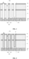
- FIG. 1 to FIG. 4 are schematic diagrams of structures corresponding to various operations in a method for manufacturing a semiconductor structure.
- a capacitance tank 106 exposing a conductive structure 101 is formed in the array area 102, and the capacitance tank 106 is configured to form a groove-type lower electrode 15.
- the substrate 10 may be divided into an array area 102 and a peripheral area 103.
- the array area 102 includes a functional area 104 in the center of the array area 102 and a buffer area 105 at the edge of the array area 102.
- the conductive structure 101 is arranged in the substrate 10.
- a width d1 of a top opening of the capacitance tank 106 is gradually reduced in a direction from the array area 102 to the peripheral area 103.
- the etching depth of the capacitance tank 106 in the buffer area 105 is relatively shallow, that is, the bottom surface of the capacitance tank 106 in the buffer area 105 may be located in the substrate 10 without exposing the conductive structure, or may be located in the first dielectric layer 11.
- the groove-type lower electrode 15 in the buffer area 105 may have an abnormal deposition thickness. Specifically, a hole is formed at the bottom portion of the groove-type lower electrode 15 due to uneven deposition thickness of the groove-type lower electrode, and the etching solution on the inner side of the groove-type lower electrode 15 may flow to the outer side of the groove-type lower electrode 15 through the hole, so as to etch the first dielectric layer 11.
- the second supporting layer 14 is etched to form a first opening 141, and the second dielectric layer 13 (with reference to FIG. 2 ) is removed through the first opening 141.
- the groove-type lower electrodes 15 with an exposed top opening are provided in the buffer area 105, and the bottom surfaces of a portion of groove-type lower electrodes 15 are located in the first dielectric layer 11.
- the etching solution for etching the second dielectric layer 13 contacts the first dielectric layer 11 through the hole at the bottom portion of the groove-type lower electrode 15 to etch the first dielectric layer 11, so that a leakage hole 111 is formed in the first dielectric layer 11.
- the leakage hole 111 may penetrate through the first dielectric layer 11.
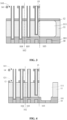
- the first supporting layer 12 is etched to form a second opening 121.
- the second supporting layer 12 in the array area 102 and the peripheral area 103 needs to be etched. Since the leakage hole 111 penetrates through the first dielectric layer 11 to expose the substrate 10, after etching through the second supporting layer 12 in the peripheral area 103, the etching solution will flow to the surface of the substrate 10 through the leakage hole 111 to continuously etch the substrate 10, so that a portion of the substrate 10 is over-etched, and even that the metal layer of the conductive structure 101 is peeled.
- the embodiments of the application provide a semiconductor structure and a method for manufacturing the semiconductor structure.
- the dielectric layer between the second supporting layer and the substrate is divided into two layers by setting the first supporting layer. Further, the etching solution flowing out of the hole at the bottom portion of the groove-type lower electrode will be only in contact with one of the dielectric layers by adjusting the position relationship between the first supporting layer and the bottom surface of the groove-type lower electrode, so that the leakage hole will only exist in one dielectric layer.
- the etching solution will not directly contact the substrate, but will be isolated by the first dielectric layer or the second dielectric layer with an intact structure, so as to ensure the structural integrity and the functional integrity of the substrate and conductive structure in the peripheral area.
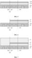
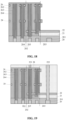
- FIG. 5 to FIG. 19 are schematic diagrams of structures corresponding to various operations in a method for manufacturing a semiconductor structure according to an embodiment of the application.
- the substrate 20 includes the array area 202 and the peripheral area 203 adjacent to the array area 202.
- the array area 202 includes a functional area 204 in the center of the array area and a buffer area 205 at the edge of the array area.
- Multiple conductive structures 201 are provided in the substrate 20, and the conductive structures 201 are arranged in the functional area 204, the buffer area 205 and the peripheral area 203.
- the material of each of the substrate 20 and the first supporting film 220 contains silicon nitride, and the silicon nitride in the substrate 20 may be used as an isolation structure to achieve an electrical isolation effect.
- the material of the first dielectric film 210 contains silicon dioxide.
- the conductive structure 201 may be a conductive contact area arranged in the substrate 20, for example an active area.
- the conductive structure 201 may also be an independent conductive plug made of the metal material, for example a tungsten block.
- the first dielectric film 210 and the first supporting film 220 in the functional area 204 are removed, the remaining portion of the first dielectric film 210 is configured as the first dielectric layer 21, and the remaining portion of the first supporting film 220 is configured as the first supporting layer 22.
- the first supporting layer 22 is not only arranged in the peripheral area 203, but also arranged in the buffer area 205.
- the first supporting layer 22 may provide support for the groove-type lower electrode subsequently formed in the buffer area 205, so as to prevent the groove-type lower electrode from being broken due to lack of support to form defects.
- the isolation of the first supporting layer 22 it is possible to retain the first dielectric layer 21 as much as possible by controlling the etching time in the wet etching process, so that the first dielectric layer 21 is avoided from being over-etched during the process of etching the second dielectric layer in contact with the first dielectric layer.
- the retained first dielectric layer 21 may be used as an additional supporting structure of the semiconductor structure to play a role of supporting the groove-type lower electrode and the conductive plug.
- the groove-type lower electrode is arranged in the buffer area 205, and the conductive plug is arranged in the peripheral area 203.
- the first dielectric layer 21 is retain, which is beneficial to avoid the upper electrode material from being deposited between the first supporting layer 22 and the substrate 20, and to reduce the process operations and shorten the process cycle without setting an addition operation for cleaning the upper electrode material or re-forming the dielectric layer for electrically isolating the upper electrode from the conductive plug.
- the second dielectric layer 23 is formed, and the second dielectric layer 23 is performed ions doping, so as to increase the etching rate of the second dielectric layer 23 in the wet etching process.
- the material of the second dielectric layer 23 may be the same as the material of the first dielectric layer 21.
- the second dielectric layer 23 is performed ions doping, which is beneficial to increase the etch selectivity ratio of the second dielectric layer 23 to the first dielectric layer 21, so that the etching of the first dielectric layer 21 with the etching solution is minimized during the process of subsequently etching the second dielectric layer 23, thereby ensuring that the first dielectric layer 21 has a relatively complete structure.
- the second supporting layer 24, the third dielectric layer 25 and the third supporting layer 26 are successively formed.
- the capacitance tanks 261 in the functional area 204 and the buffer area 205 are formed.
- each of the second supporting layer 24 and the third supporting layer 26 contains silicon nitride, and the material of the third dielectric layer 25 contains silicon dioxide.
- the capacitance tank 261 in the functional area 204 may expose the conductive structure 201 in the substrate 20, and there is gap between the bottom surface of the capacitance tank 261 in the buffer area 205 and the conductive structure 201. Specifically, the bottom surface of the capacitance tank 261 in the buffer area 205 is located in the substrate 20, the first dielectric layer 21 or the second dielectric layer 23.
- the bottom surface of the capacitance tank 261 in the buffer area 205 is located in the substrate 20 or the first dielectric layer 21.
- the second dielectric layer 23 may block the etching solution for etching the second supporting layer 24, so as to avoid the etching solution from etching the first supporting layer 22, thereby ensuring that the first supporting layer 22 may support the groove-type lower electrode in the buffer area 205.
- the bottom surface of the capacitance tank in the buffer area is located in the substrate or the second dielectric layer. It should be noted that this embodiment is based on the fact that no leakage occurs to the groove-type lower electrode of which the bottom surface is located in the substrate. When the leakage also occurs to the groove-type lower electrode of which the bottom surface is located in the substrate, the bottom surface of the groove-type lower electrode in the buffer area is limited in the first dielectric layer on the substrate, which is beneficial to avoid the leakage holes from being formed in both of the first dielectric layer and the second dielectric layer, so that the etching solution is avoided from etching through the first supporting layer to contact the substrate, thereby ensuring the preset performances of the substrate and the conductive structure.
- the height difference d2 between the bottom surface of the capacitance tank 261 and the first supporting layer 22 is comprised between 90 nm and 110 nm, for example, 95 nm, 100 nm or 105 nm. Since the hole defect usually occurs in the corner area at the bottom portion of the groove-type lower electrode, it is necessary to control the holes on the side wall of the groove-type lower electrode to be located in the first dielectric layer 21. That is, the thickness of the distribution area of the holes is less than or equal to the height difference d2, so as to ensure that the leaking etching solution only etches the first dielectric layer 21, thereby ensuring that the second dielectric layer 23 has a better structural integrity.
- the height difference d2 is vertical distance between the bottom surface of the capacitance tank 261 and the bottom surface of the first supporting layer 22, excluding the thickness of the first supporting layer 22. That is, the plugging effect of the first supporting layer 22 on the holes on the side walls of the groove-type lower electrode is not considered.
- the thickness of the first supporting layer is considered, that is, the height difference is the distance between the bottom surface of the capacitance tank and the top surface of the first supporting layer. In this way, it is beneficial to improve the position flexibility of the first supporting layer, to reduce the position accuracy requirement of the first supporting layer, and to increase the process feasibility.
- the groove-type lower electrodes 262 arranged in the buffer area 205 and the functional area 204 are formed.
- the deposition of the electrode material through the deposition process may have the problems of uneven depositing thickness and formation of holes, etc.
- the problem of formation of holes usually occurs in the corner area at the bottom portion of the groove-type lower electrode 262, thus, the smaller the width d1 of the top opening is, the more serious the problem of formation of holes is.
- Each groove-type lower electrode 262 is provided with an electrode tank 262a.
- the etching solution may contact the first dielectric layer 21 through the electrode tank 262a and the holes, so as to etch the first dielectric layer 21.
- a mask layer 27 is formed, so as to patterned etch the third supporting layer 26.
- the mask layer 27 includes a hard mask layer 271 and a photoresist layer 272.
- the photoresist layer 272 is provided with a patterned opening 272a, which is configured to define an area to be etched of the third supporting layer 26.
- the orthographic projection of the patterned opening 272a is overlapped with the orthographic projection of a portion of the groove-type lower electrodes 262, and the orthographic projection of the photoresist layer 272 is overlapped with the orthographic projection of the groove-type lower electrode 262 of which the bottom surface is located in the first dielectric layer 21.
- the third supporting layer 26 is etched to form a first opening 260.
- the photoresist layer 272 (with reference to FIG. 11 ) is removed, and the hard mask layer 271 is retained.
- the remaining portion of the hard mask layer 271 is configured to plug the top opening of the groove-type lower electrode 262, so as to avoid the etching solution from contacting the first dielectric layer 21 through the electrode tank 262a and the bottom holes when subsequently etching the third dielectric layer 25, thereby ensuring that the first dielectric layer 21 has a better structural integrity.
- the first opening 260 exposes the electrode tank 262a of a portion of the groove-type lower electrodes 262.
- the orthographic projection of the first opening is not overlapped with the orthographic projection of the groove-type lower electrode. In this way, it is beneficial to avoid the etching solution for etching the third dielectric layer from entering the electrode tank of any one of the groove-type lower electrodes, thereby further ensuring the structural integrity of each of the first dielectric layer and the second dielectric layer.
- the third dielectric layer 25 (with reference to FIG. 12 ) is removed, and the second supporting layer 24 is etched to form the second opening 241.
- the etching solution will not enter the electrode tank 262a of the specific groove-type lower electrode 262, and will not etch the first dielectric layer 21 through the bottom holes, so that the first dielectric layer 21 has a better structural integrity.
- the second supporting layer 24 and the remaining portion of the hard mark layer 271 may be simultaneously etched through a mask-less dry etching process, so as to remove the hard mask layer 271 and form the second openings 241 in the array area 202 and the peripheral area 203. Since the height difference between the top surface of the second dielectric layer 23 and the top surface of the groove-type lower electrode 262 is relatively large, when the second dielectric layer 23 is subsequently wet-etched, the etching solution is less likely to enter the electrode tank 262a. Therefore, when the second dielectric layer 23 is etched, the remaining portion of the hard mask layer 271 may be removed.
- the second dielectric layer 23 may effectively isolate the etching solution for etching the second supporting layer 24, so as to prevent the etching solution from contacting the substrate 20, thereby ensuring that the substrate 20 and the conductive structure 201 have good performances.
- the second dielectric layer 23 (with reference to FIG. 14 ) is removed.
- the capacitance structure in the buffer area 205 is usually set only to make the overall logic of the semiconductor structure correct, or to ensure that the capacitance structure in the functional area 204 is normal.
- the capacitance structure in the buffer area 205 generally does not play a role of data storage. Thus, the position of the first dielectric layer 21 in the buffer area 205 will not affect the performance of the semiconductor structure.
- a dielectric layer 263 and an upper electrode 264 are formed.
- the dielectric layer 263 covering the surface of the groove-type lower electrode 262 is formed through the deposition process.
- the upper electrode film 264a covering the first dielectric layer 21, the first supporting layer 22, the dielectric layer 263, the second supporting layer 24 and the third supporting layer 26 is formed through the deposition process.
- the upper electrode film 264a in the peripheral area 203 is removed, so as to form the upper electrode 264, so that the upper electrode 264 is avoided from electrically contacting the second conductive plug subsequently formed.
- an isolation layer 28, a first conducive plug 29 and a second conductive plug 292 are formed.
- the isolation layer 28 covering the top surface of the upper electrode 264 and filling the peripheral area 203 may be formed through the deposition process.
- the first conductive plug 291 which penetrates through the isolation layer 28 and is electrically connected to the upper electrode 264, is formed, and the second conductive plug, which penetrates through the isolation layer 28 and is connected to the conductive structure 201 in the peripheral area 203, is formed.
- the dielectric layer between the second supporting layer and the substrate is divided into two layers by forming the first supporting layer in the peripheral area, and the bottom surface of the groove-type lower electrode is located in the first dielectric layer or the second dielectric layer, so as to ensure that the leaking etching solution can only form the leakage hole in one of the dielectric layers, so that the other dielectric layer can effectively isolate the etching solution for etching the second supporting layer.
- a method for manufacturing a semiconductor structure is further provided.
- the first dielectric layer in the functional area is only doped.
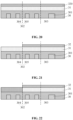
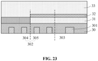
- FIG. 20 to FIG. 23 are schematic diagrams of structures corresponding to various operations in a method for manufacturing a semiconductor structure according to another embodiment of the application. The part, which is the same as or corresponds to the previous embodiment, is described with reference to the corresponding description of the previous embodiment, which is not repeated hereinafter.
- a first dielectric layer 31 and a first supporting film 320 are formed on the substrate 30.
- the first supporting film 320 covers the array area 302 and the peripheral area 303.
- the first supporting film 320 (with reference to FIG. 20 ) in the functional area 304 is removed, so as to form the first supporting layer 32 in the buffer area 305 and the peripheral area 303.
- the first dielectric layer 31 in the functional area 304 is performed ions doping, so that the etching rate of the first dielectric layer 31 in the functional area 304 in the wet etching process is increased.
- a second dielectric layer 33 covering the top surface of the first supporting layer 32 and the top surface of the first dielectric layer 31 is formed.
- a new manufacturing method is provided, so that the materials in different areas of the first dielectric layer have different etching selection ratios. In this way, it is beneficial to stop the wet etching process in time after etching the first dielectric layer 31 in the functional area 304, so as to prevent the first dielectric layer 31 in the buffer area 305 and the peripheral area 303 from being over-etched.
- an embodiment of the application further provides a semiconductor structure, which may be manufactured through the method for manufacturing the semiconductor structure described above.
- the semiconductor structure includes: a substrate 20, in which the substrate includes an array area 202 and a peripheral area 203 adjacent to the array area 202, and the array area 203 includes a buffer area 205 connected to the peripheral area 203; a first supporting layer 22 and a second supporting layer 24, in which the first supporting layer 22 is arranged in the peripheral area 203, the second supporting layer 24 is arranged in the array area 202, and the second supporting layer 24 is higher than the first supporting layer 22; a groove-type lower electrode 262, in which the groove-type lower electrode 262 is arranged in the buffer area 205 and penetrates through the second supporting layer 24, a bottom surface the groove-type lower electrode 262 is higher than a surface of the substrate 20 and lower than the first supporting layer 22, or a bottom surface the groove-type lower electrode 262 is higher than the first supporting layer 22 and lower than the second supporting layer 24.
- the bottom surface of the groove-type lower electrode 262 is higher than the surface of the substrate 20 and lower than the first supporting layer 22.
- the first supporting layer 22 is also arranged in the buffer area 205 and configured to support the groove-type lower electrode 262.
- the height difference between the bottom surface of the groove-type lower electrode 262 and the first supporting layer 22 is comprised between 90 nm and 110 nm, for example, 95 nm, 100 nm or 105 nm.
- a conductive structure 201 is provided in the substrate 20.
- the semiconductor structure further includes a first dielectric layer 21 arranged between the first supporting layer 22 and the substrate 20.
- a first dielectric layer 21 arranged between the first supporting layer 22 and the substrate 20.
- an orthographic projection of at least one conductive structure 201 in the peripheral area 203 is located in an orthographic projection of the first dielectric layer 21. In this way, it is beneficial to ensure that the first dielectric layer 21 can isolate the second conductive plug 292 from the upper electrode 264.
- the semiconductor structure further includes: an upper electrode 264, in which the upper electrode 264 covers an inner wall and an outer wall of the groove-type lower electrode 264 to form a double-sided capacitance structure, and a dielectric layer 263 is provided between the upper electrode 264 and the groove-type lower electrode 262; a first conductive plug 291 electrically connected to the upper electrode 264; and a second conductive plug 292 electrically connected to at least one conductive structure 201 in the peripheral area 203.
- the semiconductor structure further includes: a third supporting layer 26, in which the third supporting layer 26 is arranged in the array area 202 and higher than the second supporting layer 24, and the groove-type lower electrode 262 penetrates through the third supporting layer 26; and an isolation layer 28, in which the isolation layer is arranged in the array area 202 and the peripheral area 203, and each of the first conductive plug 291 and the second conductive plug 292 penetrates through the isolation layer 292.
- a semiconductor structure in this embodiment, includes a first supporting layer arranged in the peripheral area.
- the first supporting layer may be configured to define the etching range of the etching solution flowing out of the bottom portion of the groove-type lower electrode, so as to ensure the integrity of the structures in other areas, thereby protecting the substrate.
Landscapes
- Engineering & Computer Science (AREA)
- Manufacturing & Machinery (AREA)
- Semiconductor Memories (AREA)
Abstract
Description
- This application claims priority to
Chinese Patent Application No. 202010956160.9, filed on September 11, 2020 - An embodiment of the application relates to the field of semiconductors, in particular to a semiconductor structure and a method for manufacturing the semiconductor structure.
- As the size of the semiconductor structure shrinks, it becomes more and more difficult to increase or maintain the capacitance value of an individual capacitance structure. When using the same dielectric layer material, the capacitance value may be increased only by increasing the surface area of an electrode plate or reducing the thickness of a dielectric layer.
- At present, the capacitance structure usually adopts a double-sided capacitance structure with a supporting layer. During the formation of the double-sided capacitance structure, etching defects frequently occur due to the edge size effect of a capacitor array and the etching load effect.
- An embodiment of the application provides a semiconductor structure and a method for manufacturing the semiconductor structure, which are beneficial to avoid damage to a substrate in a peripheral area.
- According to a first aspect of the embodiments of the application, a method for manufacturing a semiconductor structure is provided. The method includes the following operations. A substrate is provided, in which the substrate includes an array area and a peripheral area adjacent to the array area, and the array area includes a buffer area connected to the peripheral area. A first dielectric layer, a first supporting layer, a second dielectric layer, a second supporting layer and a third dielectric layer, which are successively stacked onto one another, are formed on the substrate, in which the first supporting layer is arranged at least in the peripheral area, the first dielectric layer is arranged between the first supporting layer and the substrate, the second dielectric layer covers the first supporting layer and the substrate, and each of the second supporting layer and the third dielectric layer is arranged in the array area and the peripheral area. A groove-type lower electrode, which at least penetrates through the third dielectric layer and the second supporting layer, is formed in the buffer area, in which a bottom surface the groove-type lower electrode is located in the first dielectric layer or in the second dielectric layer. The third dielectric layer is removed through a wet etching process. The second supporting layer in the peripheral area is etched after removing the third dielectric layer.
- According to a second aspect of the embodiments of the application, a semiconductor structure is provided. The semiconductor structure includes: a substrate, in which the substrate includes an array area and a peripheral area adjacent to the array area, and the array area includes a buffer area connected to the peripheral area; a first supporting layer and a second supporting layer, in which the first supporting layer is arranged in the peripheral area, the second supporting layer is arranged in the array area, and the second supporting layer is higher than the first supporting layer; and a groove-type lower electrode, in which the groove-type lower electrode is arranged in the buffer area and penetrates through the second supporting layer, a bottom surface the groove-type lower electrode is higher than a surface of the substrate and lower than the first supporting layer, or a bottom surface of the groove-type lower electrode is higher than the first supporting layer and lower than the second supporting layer.
- Compared with the related art, the technical solutions provided by the embodiments of the application have the following advantages.
- In the abovementioned technical solutions, the dielectric layer between the second supporting layer and the substrate is divided into the first dielectric layer and the second dielectric layer through a first isolation layer. If the bottom portion of the groove-type lower electrode has a hole defect, and the etching solution may leak through the hole defect, in a process of etching the third dielectric layer, only one of the first dielectric layer and the second dielectric layer will be etched by the leaking etching solution, so as to form a leakage hole. That is to say, at least one of the first dielectric layer and the second dielectric layer between the second supporting layer and the substrate in the peripheral area is intact. In this way, when the second supporting layer in the peripheral area is removed by etching, the etching solution will not directly contact the substrate in the peripheral area due to the existence of the leakage hole, so as to avoid damage to the substrate in the peripheral area.
- One or more embodiments are exemplarily explained through the figures in the accompanying drawings corresponding thereto, these exemplary explanations do not constitute a limitation to the embodiments; and unless otherwise specifically declared, the figures in the accompanying drawings do not constitute a limitation of proportion.
-
FIG. 1-FIG. 4 are schematic sectional diagrams of structures corresponding to various operations in a method for manufacturing a semiconductor structure; -
FIG. 5-FIG. 19 are schematic diagrams of structures corresponding to various operations in a method for manufacturing a semiconductor structure according to an embodiment of the application; and -
FIG. 20-FIG. 23 are schematic diagrams of structures corresponding to various operations in a method for manufacturing a semiconductor structure according to another embodiment of the application. -
FIG. 1 to FIG. 4 are schematic diagrams of structures corresponding to various operations in a method for manufacturing a semiconductor structure. - With reference to
FIG. 1 and FIG. 2 , acapacitance tank 106 exposing aconductive structure 101 is formed in thearray area 102, and thecapacitance tank 106 is configured to form a groove-typelower electrode 15. - The
substrate 10 may be divided into anarray area 102 and aperipheral area 103. Thearray area 102 includes afunctional area 104 in the center of thearray area 102 and abuffer area 105 at the edge of thearray area 102. Theconductive structure 101 is arranged in thesubstrate 10. - During the formation of the
capacitance tank 106, due to the edge size effect, a width d1 of a top opening of thecapacitance tank 106 is gradually reduced in a direction from thearray area 102 to theperipheral area 103. Meanwhile, due to the etching load effect, the etching depth of thecapacitance tank 106 in thebuffer area 105 is relatively shallow, that is, the bottom surface of thecapacitance tank 106 in thebuffer area 105 may be located in thesubstrate 10 without exposing the conductive structure, or may be located in the firstdielectric layer 11. - In addition, during the formation of the groove-type
lower electrode 15 by performing a deposition process, since the width d1 of the top opening of thecapacitance tank 106 in thebuffer area 105 is relatively small, and the depth-to-width ratio is slightly larger, it is difficult for the electrode material to uniformly cover any surface of thecapacitance tank 106. Thus, the groove-typelower electrode 15 in thebuffer area 105 may have an abnormal deposition thickness. Specifically, a hole is formed at the bottom portion of the groove-typelower electrode 15 due to uneven deposition thickness of the groove-type lower electrode, and the etching solution on the inner side of the groove-typelower electrode 15 may flow to the outer side of the groove-typelower electrode 15 through the hole, so as to etch the firstdielectric layer 11. - With reference to
FIG. 3 , the second supportinglayer 14 is etched to form afirst opening 141, and the second dielectric layer 13 (with reference toFIG. 2 ) is removed through thefirst opening 141. - During the etching of the second
dielectric layer 13, the groove-typelower electrodes 15 with an exposed top opening are provided in thebuffer area 105, and the bottom surfaces of a portion of groove-typelower electrodes 15 are located in the firstdielectric layer 11. Thus, the etching solution for etching the seconddielectric layer 13 contacts the firstdielectric layer 11 through the hole at the bottom portion of the groove-typelower electrode 15 to etch the firstdielectric layer 11, so that aleakage hole 111 is formed in the firstdielectric layer 11. Theleakage hole 111 may penetrate through the firstdielectric layer 11. - With reference to
FIG. 4 , the first supportinglayer 12 is etched to form asecond opening 121. - During the formation of the
second opening 121, the second supportinglayer 12 in thearray area 102 and theperipheral area 103 needs to be etched. Since theleakage hole 111 penetrates through the firstdielectric layer 11 to expose thesubstrate 10, after etching through the second supportinglayer 12 in theperipheral area 103, the etching solution will flow to the surface of thesubstrate 10 through theleakage hole 111 to continuously etch thesubstrate 10, so that a portion of thesubstrate 10 is over-etched, and even that the metal layer of theconductive structure 101 is peeled. - In order to solve the abovementioned problem, the embodiments of the application provide a semiconductor structure and a method for manufacturing the semiconductor structure. The dielectric layer between the second supporting layer and the substrate is divided into two layers by setting the first supporting layer. Further, the etching solution flowing out of the hole at the bottom portion of the groove-type lower electrode will be only in contact with one of the dielectric layers by adjusting the position relationship between the first supporting layer and the bottom surface of the groove-type lower electrode, so that the leakage hole will only exist in one dielectric layer. In this way, during the process of etching the second supporting layer, even if the second supporting layer is etched through, the etching solution will not directly contact the substrate, but will be isolated by the first dielectric layer or the second dielectric layer with an intact structure, so as to ensure the structural integrity and the functional integrity of the substrate and conductive structure in the peripheral area.
- In order to make the objectives, technical solution and advantages of the embodiments of the application more apparent, hereinafter, the respective embodiments of the application will be described in detail in connection with the accompanying drawings. However, those ordinary skilled in the art may understand that, in the respective embodiments of the application, numerous technical details are set forth in order to provide a reader with a better understanding of the application. However, the technical solutions claimed in the application can also be implemented without these technical details and various changes and modifications based on the respective embodiments below.
-
FIG. 5 to FIG. 19 are schematic diagrams of structures corresponding to various operations in a method for manufacturing a semiconductor structure according to an embodiment of the application. - With reference to
FIG. 5 , thesubstrate 20, as well as a firstdielectric film 210 and a first supportingfilm 220 which are arranged on thesubstrate 20, are provided - The
substrate 20 includes thearray area 202 and theperipheral area 203 adjacent to thearray area 202. Thearray area 202 includes afunctional area 204 in the center of the array area and abuffer area 205 at the edge of the array area. Multipleconductive structures 201 are provided in thesubstrate 20, and theconductive structures 201 are arranged in thefunctional area 204, thebuffer area 205 and theperipheral area 203. - In this embodiment, the material of each of the
substrate 20 and the first supportingfilm 220 contains silicon nitride, and the silicon nitride in thesubstrate 20 may be used as an isolation structure to achieve an electrical isolation effect. The material of the firstdielectric film 210 contains silicon dioxide. Theconductive structure 201 may be a conductive contact area arranged in thesubstrate 20, for example an active area. Theconductive structure 201 may also be an independent conductive plug made of the metal material, for example a tungsten block. - With reference to
FIG. 6 , the firstdielectric film 210 and the first supportingfilm 220 in thefunctional area 204 are removed, the remaining portion of the firstdielectric film 210 is configured as the firstdielectric layer 21, and the remaining portion of the first supportingfilm 220 is configured as the first supportinglayer 22. - In this embodiment, the first supporting
layer 22 is not only arranged in theperipheral area 203, but also arranged in thebuffer area 205. The first supportinglayer 22 may provide support for the groove-type lower electrode subsequently formed in thebuffer area 205, so as to prevent the groove-type lower electrode from being broken due to lack of support to form defects. - In addition, due to the isolation of the first supporting
layer 22, it is possible to retain thefirst dielectric layer 21 as much as possible by controlling the etching time in the wet etching process, so that thefirst dielectric layer 21 is avoided from being over-etched during the process of etching the second dielectric layer in contact with the first dielectric layer. - The retained
first dielectric layer 21 may be used as an additional supporting structure of the semiconductor structure to play a role of supporting the groove-type lower electrode and the conductive plug. The groove-type lower electrode is arranged in thebuffer area 205, and the conductive plug is arranged in theperipheral area 203. In addition, thefirst dielectric layer 21 is retain, which is beneficial to avoid the upper electrode material from being deposited between the first supportinglayer 22 and thesubstrate 20, and to reduce the process operations and shorten the process cycle without setting an addition operation for cleaning the upper electrode material or re-forming the dielectric layer for electrically isolating the upper electrode from the conductive plug. - With reference to
FIG. 7 andFIG. 8 , thesecond dielectric layer 23 is formed, and thesecond dielectric layer 23 is performed ions doping, so as to increase the etching rate of thesecond dielectric layer 23 in the wet etching process. - In this embodiment, the material of the
second dielectric layer 23 may be the same as the material of thefirst dielectric layer 21. In this embodiment, thesecond dielectric layer 23 is performed ions doping, which is beneficial to increase the etch selectivity ratio of thesecond dielectric layer 23 to thefirst dielectric layer 21, so that the etching of thefirst dielectric layer 21 with the etching solution is minimized during the process of subsequently etching thesecond dielectric layer 23, thereby ensuring that thefirst dielectric layer 21 has a relatively complete structure. - With reference to
FIG. 9 , the second supportinglayer 24, thethird dielectric layer 25 and the third supportinglayer 26 are successively formed. Thecapacitance tanks 261 in thefunctional area 204 and thebuffer area 205 are formed. - The material of each of the second supporting
layer 24 and the third supportinglayer 26 contains silicon nitride, and the material of thethird dielectric layer 25 contains silicon dioxide. - Due to the edge size effect and the etching load effect, the
capacitance tank 261 in thefunctional area 204 may expose theconductive structure 201 in thesubstrate 20, and there is gap between the bottom surface of thecapacitance tank 261 in thebuffer area 205 and theconductive structure 201. Specifically, the bottom surface of thecapacitance tank 261 in thebuffer area 205 is located in thesubstrate 20, thefirst dielectric layer 21 or thesecond dielectric layer 23. - In this embodiment, the bottom surface of the
capacitance tank 261 in thebuffer area 205 is located in thesubstrate 20 or thefirst dielectric layer 21. In this way, when the etching solution leaks, the leakage hole is only formed in thefirst dielectric layer 21, and thesecond dielectric layer 23 may be kept intact. Thesecond dielectric layer 23 may block the etching solution for etching the second supportinglayer 24, so as to avoid the etching solution from etching the first supportinglayer 22, thereby ensuring that the first supportinglayer 22 may support the groove-type lower electrode in thebuffer area 205. - In some embodiments, the bottom surface of the capacitance tank in the buffer area is located in the substrate or the second dielectric layer. It should be noted that this embodiment is based on the fact that no leakage occurs to the groove-type lower electrode of which the bottom surface is located in the substrate. When the leakage also occurs to the groove-type lower electrode of which the bottom surface is located in the substrate, the bottom surface of the groove-type lower electrode in the buffer area is limited in the first dielectric layer on the substrate, which is beneficial to avoid the leakage holes from being formed in both of the first dielectric layer and the second dielectric layer, so that the etching solution is avoided from etching through the first supporting layer to contact the substrate, thereby ensuring the preset performances of the substrate and the conductive structure.
- In this embodiment, in a direction perpendicular to the surface of the
substrate 20, the height difference d2 between the bottom surface of thecapacitance tank 261 and the first supportinglayer 22 is comprised between 90 nm and 110 nm, for example, 95 nm, 100 nm or 105 nm. Since the hole defect usually occurs in the corner area at the bottom portion of the groove-type lower electrode, it is necessary to control the holes on the side wall of the groove-type lower electrode to be located in thefirst dielectric layer 21. That is, the thickness of the distribution area of the holes is less than or equal to the height difference d2, so as to ensure that the leaking etching solution only etches thefirst dielectric layer 21, thereby ensuring that thesecond dielectric layer 23 has a better structural integrity. - In this embodiment, the height difference d2 is vertical distance between the bottom surface of the
capacitance tank 261 and the bottom surface of the first supportinglayer 22, excluding the thickness of the first supportinglayer 22. That is, the plugging effect of the first supportinglayer 22 on the holes on the side walls of the groove-type lower electrode is not considered. - In some embodiments, the thickness of the first supporting layer is considered, that is, the height difference is the distance between the bottom surface of the capacitance tank and the top surface of the first supporting layer. In this way, it is beneficial to improve the position flexibility of the first supporting layer, to reduce the position accuracy requirement of the first supporting layer, and to increase the process feasibility.
- With reference to
FIG. 10 , in the same formation process, the groove-typelower electrodes 262 arranged in thebuffer area 205 and thefunctional area 204 are formed. - During the process of forming the groove-type
lower electrodes 262, since the width d1 of the top opening of thecapacitance tank 261 in thebuffer area 205 is relatively small, and the depth-to-width ratio is relatively large, the deposition of the electrode material through the deposition process may have the problems of uneven depositing thickness and formation of holes, etc. The problem of formation of holes usually occurs in the corner area at the bottom portion of the groove-typelower electrode 262, thus, the smaller the width d1 of the top opening is, the more serious the problem of formation of holes is. - Each groove-type
lower electrode 262 is provided with anelectrode tank 262a. The etching solution may contact thefirst dielectric layer 21 through theelectrode tank 262a and the holes, so as to etch thefirst dielectric layer 21. - With reference to
FIG. 11 , amask layer 27 is formed, so as to patterned etch the third supportinglayer 26. - The
mask layer 27 includes ahard mask layer 271 and aphotoresist layer 272. Thephotoresist layer 272 is provided with apatterned opening 272a, which is configured to define an area to be etched of the third supportinglayer 26. - In this embodiment, in the direction perpendicular to the surface of the
substrate 20, the orthographic projection of the patternedopening 272a is overlapped with the orthographic projection of a portion of the groove-typelower electrodes 262, and the orthographic projection of thephotoresist layer 272 is overlapped with the orthographic projection of the groove-typelower electrode 262 of which the bottom surface is located in thefirst dielectric layer 21. In this way, it is beneficial to ensure that the remaining portion of themask layer 27 may plug the top opening of the specific groove-typelower electrode 262 after etching the third supportinglayer 26. - With reference to
FIG. 12 , the third supportinglayer 26 is etched to form afirst opening 260. - In this embodiment, after forming the
first opening 260, the photoresist layer 272 (with reference toFIG. 11 ) is removed, and thehard mask layer 271 is retained. The remaining portion of thehard mask layer 271 is configured to plug the top opening of the groove-typelower electrode 262, so as to avoid the etching solution from contacting thefirst dielectric layer 21 through theelectrode tank 262a and the bottom holes when subsequently etching thethird dielectric layer 25, thereby ensuring that thefirst dielectric layer 21 has a better structural integrity. - In this embodiment, the
first opening 260 exposes theelectrode tank 262a of a portion of the groove-typelower electrodes 262. In other embodiments, in the direction perpendicular to the surface of the substrate, the orthographic projection of the first opening is not overlapped with the orthographic projection of the groove-type lower electrode. In this way, it is beneficial to avoid the etching solution for etching the third dielectric layer from entering the electrode tank of any one of the groove-type lower electrodes, thereby further ensuring the structural integrity of each of the first dielectric layer and the second dielectric layer. - With reference to
FIG. 13 andFIG. 14 , the third dielectric layer 25 (with reference toFIG. 12 ) is removed, and the second supportinglayer 24 is etched to form thesecond opening 241. - During the process of removing the
third dielectric layer 25, due to the plugging of thehard mask layer 271, the etching solution will not enter theelectrode tank 262a of the specific groove-typelower electrode 262, and will not etch thefirst dielectric layer 21 through the bottom holes, so that thefirst dielectric layer 21 has a better structural integrity. - In this embodiment, the second supporting
layer 24 and the remaining portion of thehard mark layer 271 may be simultaneously etched through a mask-less dry etching process, so as to remove thehard mask layer 271 and form thesecond openings 241 in thearray area 202 and theperipheral area 203. Since the height difference between the top surface of thesecond dielectric layer 23 and the top surface of the groove-typelower electrode 262 is relatively large, when thesecond dielectric layer 23 is subsequently wet-etched, the etching solution is less likely to enter theelectrode tank 262a. Therefore, when thesecond dielectric layer 23 is etched, the remaining portion of thehard mask layer 271 may be removed. - In this embodiment, during the process of removing the second supporting
layer 24 in theperipheral area 203, since thesecond dielectric layer 23 has a better structural integrity, and the etch selectivity ratio of thesecond dielectric layer 23 to the second supportinglayer 24 is relatively large, thesecond dielectric layer 23 may effectively isolate the etching solution for etching the second supportinglayer 24, so as to prevent the etching solution from contacting thesubstrate 20, thereby ensuring that thesubstrate 20 and theconductive structure 201 have good performances. - With reference to
FIG. 15 , the second dielectric layer 23 (with reference toFIG. 14 ) is removed. - In this embodiment, since the
first dielectric layer 21 contacts thesecond dielectric layer 23, a portion of thefirst dielectric layer 21 may be removed by etching when thesecond dielectric layer 23 is etched, and the remaining portion of thefirst dielectric layer 21 may play a role of electrical isolation and support. It should be noted that the capacitance structure in thebuffer area 205 is usually set only to make the overall logic of the semiconductor structure correct, or to ensure that the capacitance structure in thefunctional area 204 is normal. The capacitance structure in thebuffer area 205 generally does not play a role of data storage. Thus, the position of thefirst dielectric layer 21 in thebuffer area 205 will not affect the performance of the semiconductor structure. - With reference to
FIG. 16 to FIG. 18 , adielectric layer 263 and anupper electrode 264 are formed. - In this embodiment, the
dielectric layer 263 covering the surface of the groove-typelower electrode 262 is formed through the deposition process. The upper electrode film 264a covering thefirst dielectric layer 21, the first supportinglayer 22, thedielectric layer 263, the second supportinglayer 24 and the third supportinglayer 26 is formed through the deposition process. After forming the upper electrode film 264a, the upper electrode film 264a in theperipheral area 203 is removed, so as to form theupper electrode 264, so that theupper electrode 264 is avoided from electrically contacting the second conductive plug subsequently formed. - With reference to
FIG. 19 , anisolation layer 28, a first conducive plug 29 and a secondconductive plug 292 are formed. - In this embodiment, after forming the
upper electrode 264, theisolation layer 28 covering the top surface of theupper electrode 264 and filling theperipheral area 203 may be formed through the deposition process. After forming theisolation layer 28, the firstconductive plug 291, which penetrates through theisolation layer 28 and is electrically connected to theupper electrode 264, is formed, and the second conductive plug, which penetrates through theisolation layer 28 and is connected to theconductive structure 201 in theperipheral area 203, is formed. - In this embodiment, the dielectric layer between the second supporting layer and the substrate is divided into two layers by forming the first supporting layer in the peripheral area, and the bottom surface of the groove-type lower electrode is located in the first dielectric layer or the second dielectric layer, so as to ensure that the leaking etching solution can only form the leakage hole in one of the dielectric layers, so that the other dielectric layer can effectively isolate the etching solution for etching the second supporting layer.
- According to another embodiment of the application, a method for manufacturing a semiconductor structure is further provided. Different from the previous embodiment, in this embodiment, the first dielectric layer in the functional area is only doped. Detail description is made in combination with
FIG. 20 to FIG. 23. FIG. 20 to FIG. 23 are schematic diagrams of structures corresponding to various operations in a method for manufacturing a semiconductor structure according to another embodiment of the application. The part, which is the same as or corresponds to the previous embodiment, is described with reference to the corresponding description of the previous embodiment, which is not repeated hereinafter. - With reference to
FIG. 20 , afirst dielectric layer 31 and a first supportingfilm 320 are formed on thesubstrate 30. The first supportingfilm 320 covers thearray area 302 and theperipheral area 303. - With reference to
FIG. 21 , the first supporting film 320 (with reference toFIG. 20 ) in thefunctional area 304 is removed, so as to form the first supportinglayer 32 in thebuffer area 305 and theperipheral area 303. With reference toFIG. 22 , by using the first supportinglayer 32 as a mask, thefirst dielectric layer 31 in thefunctional area 304 is performed ions doping, so that the etching rate of thefirst dielectric layer 31 in thefunctional area 304 in the wet etching process is increased. - With reference to
FIG. 23 , asecond dielectric layer 33 covering the top surface of the first supportinglayer 32 and the top surface of thefirst dielectric layer 31 is formed. - In this embodiment, a new manufacturing method is provided, so that the materials in different areas of the first dielectric layer have different etching selection ratios. In this way, it is beneficial to stop the wet etching process in time after etching the
first dielectric layer 31 in thefunctional area 304, so as to prevent thefirst dielectric layer 31 in thebuffer area 305 and theperipheral area 303 from being over-etched. - Correspondingly, an embodiment of the application further provides a semiconductor structure, which may be manufactured through the method for manufacturing the semiconductor structure described above.
- With reference to
FIG. 19 , the semiconductor structure includes: asubstrate 20, in which the substrate includes anarray area 202 and aperipheral area 203 adjacent to thearray area 202, and thearray area 203 includes abuffer area 205 connected to theperipheral area 203; a first supportinglayer 22 and a second supportinglayer 24, in which the first supportinglayer 22 is arranged in theperipheral area 203, the second supportinglayer 24 is arranged in thearray area 202, and the second supportinglayer 24 is higher than the first supportinglayer 22; a groove-typelower electrode 262, in which the groove-typelower electrode 262 is arranged in thebuffer area 205 and penetrates through the second supportinglayer 24, a bottom surface the groove-typelower electrode 262 is higher than a surface of thesubstrate 20 and lower than the first supportinglayer 22, or a bottom surface the groove-typelower electrode 262 is higher than the first supportinglayer 22 and lower than the second supportinglayer 24. - In this embodiment, the bottom surface of the groove-type
lower electrode 262 is higher than the surface of thesubstrate 20 and lower than the first supportinglayer 22. The first supportinglayer 22 is also arranged in thebuffer area 205 and configured to support the groove-typelower electrode 262. - In this embodiment, in a direction perpendicular to the surface of the
substrate 20, the height difference between the bottom surface of the groove-typelower electrode 262 and the first supportinglayer 22 is comprised between 90 nm and 110 nm, for example, 95 nm, 100 nm or 105 nm. - In this embodiment, a
conductive structure 201 is provided in thesubstrate 20. The semiconductor structure further includes afirst dielectric layer 21 arranged between the first supportinglayer 22 and thesubstrate 20. In a direction perpendicular to the surface of thesubstrate 20, an orthographic projection of at least oneconductive structure 201 in theperipheral area 203 is located in an orthographic projection of thefirst dielectric layer 21. In this way, it is beneficial to ensure that thefirst dielectric layer 21 can isolate the secondconductive plug 292 from theupper electrode 264. - In this embodiment, the semiconductor structure further includes: an
upper electrode 264, in which theupper electrode 264 covers an inner wall and an outer wall of the groove-typelower electrode 264 to form a double-sided capacitance structure, and adielectric layer 263 is provided between theupper electrode 264 and the groove-typelower electrode 262; a firstconductive plug 291 electrically connected to theupper electrode 264; and a secondconductive plug 292 electrically connected to at least oneconductive structure 201 in theperipheral area 203. - In this embodiment, the semiconductor structure further includes: a third supporting
layer 26, in which the third supportinglayer 26 is arranged in thearray area 202 and higher than the second supportinglayer 24, and the groove-typelower electrode 262 penetrates through the third supportinglayer 26; and anisolation layer 28, in which the isolation layer is arranged in thearray area 202 and theperipheral area 203, and each of the firstconductive plug 291 and the secondconductive plug 292 penetrates through theisolation layer 292. - In this embodiment, a semiconductor structure is provided. The semiconductor structure includes a first supporting layer arranged in the peripheral area. The first supporting layer may be configured to define the etching range of the etching solution flowing out of the bottom portion of the groove-type lower electrode, so as to ensure the integrity of the structures in other areas, thereby protecting the substrate.
- Those of ordinary skill in the art may understand that the above embodiments are specific embodiments to implement the application. In practical applications, various changes may be made in forms and details without deviating from the spirit and scope of the application. Any person skilled in the art may make change and modifications without deviating from the spirit and scope of the application. Therefore, the protection scope of the application should be subjected the scope defined by the appended claims.
Claims (13)
- A method for manufacturing a semiconductor structure, comprising:providing a substrate, wherein the substrate comprises an array area and a peripheral area adjacent to the array area, and the array area comprises a buffer area connected to the peripheral area;forming a first dielectric layer, a first supporting layer, a second dielectric layer, a second supporting layer and a third dielectric layer, which are successively stacked onto one another, on the substrate, wherein the first supporting layer is arranged at least in the peripheral area, the first dielectric layer is arranged between the first supporting layer and the substrate, the second dielectric layer covers the first supporting layer and the substrate, and each of the second supporting layer and the third dielectric layer is arranged in the array area and the peripheral area;forming a groove-type lower electrode, which at least penetrates through the third dielectric layer and the second supporting layer, in the buffer area, wherein a bottom surface of the groove-type lower electrode is located in the first dielectric layer or in the second dielectric layer;removing the third dielectric layer through a wet etching process; andetching the second supporting layer in the peripheral area after removing the third dielectric layer.
- The method for manufacturing the semiconductor structure of claim 1, wherein the method comprises: removing the second dielectric layer after etching the second supporting layer.
- The method for manufacturing the semiconductor structure of claim 2, wherein the method comprises: after forming the second dielectric layer and before forming the second supporting layer, performing ions doping to the second dielectric layer to increase an etching rate of the second dielectric layer in the wet etching process.
- The method for manufacturing the semiconductor structure of claim 2, wherein a conductive structure is provided in the substrate, and the method comprises: forming an upper electrode covering an inner wall and an outer wall of the groove-type lower electrode after removing the second dielectric layer; and forming a first conductive plug and a second conductive plug, the first conductive plug being electrically connected to the upper electrode, and the second conductive plug being electrically connected to the conductive structure in the peripheral area.
- The method for manufacturing the semiconductor structure of claim 4, wherein the method comprises: forming an upper electrode film covering a surface of the first supporting layer, a surface of the second supporting layer and a surface of the groove-type lower electrode through a deposition process; removing the upper electrode film in the peripheral area to form the upper electrode; forming an isolation layer arranged in the array area and in the peripheral area through a deposition process; and forming the first conductive plug and the second conductive plug which penetrate through the isolation layer, the isolation layer isolating the upper electrode from the second conductive plug.
- The method for manufacturing the semiconductor structure of claim 1, wherein the array area comprises a functional area in a center of the array area and the buffer area at an edge of the array area, and wherein a plurality of groove-type lower electrodes in the buffer area and in the functional area are formed through a same formation process, a width of an opening of each groove-type lower electrode in the functional area being greater than a width of an opening of each groove-type lower electrode in the buffer area in a direction from the array area to the peripheral area.
- The method for manufacturing the semiconductor structure of claim 1, wherein the method comprises: forming a third supporting layer covering the third dielectric layer after forming the third dielectric layer, and wherein removing the third dielectric layer comprises: etching the third supporting layer to form a first opening, and etching and removing the third dielectric layer through the first opening.
- A semiconductor structure, comprising:a substrate, wherein the substrate comprises an array area and a peripheral area adjacent to the array area, and the array area comprises a buffer area connected to the peripheral area;a first supporting layer and a second supporting layer, wherein the first supporting layer is arranged in the peripheral area, the second supporting layer is arranged in the array area, and the second supporting layer is higher than the first supporting layer; anda groove-type lower electrode, wherein the groove-type lower electrode is arranged in the buffer area and penetrates through the second supporting layer, a bottom surface of the groove-type lower electrode is higher than a surface of the substrate and lower than the first supporting layer, or a bottom surface of the groove-type lower electrode is higher than the first supporting layer and lower than the second supporting layer.
- The semiconductor structure of claim 8, wherein the bottom surface of the groove-type lower electrode is higher than the surface of the substrate and lower than the first supporting layer, and the first supporting layer is also arranged in the buffer area and configured to support the groove-type lower electrode.
- The semiconductor structure of claim 8, wherein the bottom surface of the groove-type lower electrode is higher than the surface of the substrate and lower than the first supporting layer, and a height difference between the bottom surface of the groove-type lower electrode and the first supporting layer is comprised between 90 nm and 110 nm in a direction perpendicular to the surface of the substrate.
- The semiconductor structure of claim 8, wherein a plurality of conductive structures are provided in the substrate, and the semiconductor structure further comprises a first dielectric layer arranged between the first supporting layer and the substrate, and wherein an orthographic projection of at least one of the conductive structures in the peripheral area is located in an orthographic projection of the first dielectric layer in a direction perpendicular to the surface of the substrate.
- The semiconductor structure of claim 8, further comprising an upper electrode covering an inner wall and an outer wall of the groove-type lower electrode; a first conductive plug electrically connected to the upper electrode; and a second conductive plug electrically connected to at least one conductive structure in the peripheral area.
- The semiconductor structure of claim 12, further comprising: a third supporting layer, the third supporting layer being arranged in the array area and higher than the second supporting layer, and the groove-type lower electrode penetrating through the third supporting layer; and an isolation layer, the isolation layer being arranged in the array area and the peripheral area, and the first conductive plug and the second conductive plug penetrating through the isolation layer.
Applications Claiming Priority (2)
| Application Number | Priority Date | Filing Date | Title |
|---|---|---|---|
| CN202010956160.9A CN114171463B (en) | 2020-09-11 | 2020-09-11 | Semiconductor structure and method for manufacturing the same |
| PCT/CN2021/103854 WO2022052599A1 (en) | 2020-09-11 | 2021-06-30 | Semiconductor structure and manufacturing method therefor |
Publications (2)
| Publication Number | Publication Date |
|---|---|
| EP4195252A1 true EP4195252A1 (en) | 2023-06-14 |
| EP4195252A4 EP4195252A4 (en) | 2024-01-17 |
Family
ID=80627995
Family Applications (1)
| Application Number | Title | Priority Date | Filing Date |
|---|---|---|---|
| EP21865655.1A Pending EP4195252A4 (en) | 2020-09-11 | 2021-06-30 | Semiconductor structure and manufacturing method therefor |
Country Status (2)
| Country | Link |
|---|---|
| US (1) | US11955511B2 (en) |
| EP (1) | EP4195252A4 (en) |
Families Citing this family (3)
| Publication number | Priority date | Publication date | Assignee | Title |
|---|---|---|---|---|
| US11901405B2 (en) * | 2020-09-11 | 2024-02-13 | Changxin Memory Technologies, Inc. | Semiconductor structure and method for manufacturing semiconductor structure |
| CN113539955B (en) * | 2021-08-05 | 2024-02-06 | 长鑫存储技术有限公司 | Semiconductor structure and manufacturing method thereof |
| CN119255600B (en) * | 2024-10-21 | 2026-05-12 | 福建省晋华集成电路有限公司 | Semiconductor device and manufacturing method thereof |
Family Cites Families (15)
| Publication number | Priority date | Publication date | Assignee | Title |
|---|---|---|---|---|
| JP4056588B2 (en) * | 1996-11-06 | 2008-03-05 | 富士通株式会社 | Semiconductor device and manufacturing method thereof |
| US7387939B2 (en) * | 2004-07-19 | 2008-06-17 | Micron Technology, Inc. | Methods of forming semiconductor structures and capacitor devices |
| DE102007054077A1 (en) | 2007-11-13 | 2009-07-23 | Qimonda Ag | Method for producing an integrated circuit and arrangement with a substrate |
| US8274777B2 (en) | 2008-04-08 | 2012-09-25 | Micron Technology, Inc. | High aspect ratio openings |
| US7618874B1 (en) * | 2008-05-02 | 2009-11-17 | Micron Technology, Inc. | Methods of forming capacitors |
| US9076680B2 (en) | 2011-10-18 | 2015-07-07 | Micron Technology, Inc. | Integrated circuitry, methods of forming capacitors, and methods of forming integrated circuitry comprising an array of capacitors and circuitry peripheral to the array |
| US9001565B2 (en) * | 2012-04-25 | 2015-04-07 | Ps4 Luxco S.A.R.L. | Semiconductor device with memory device |
| US9041154B2 (en) | 2013-03-06 | 2015-05-26 | Nanya Technology Corp. | Contact structure and semiconductor memory device using the same |
| KR102738401B1 (en) * | 2016-12-07 | 2024-12-04 | 삼성전자주식회사 | Semiconductor device |
| CN107706206A (en) | 2017-11-02 | 2018-02-16 | 睿力集成电路有限公司 | Array of capacitors and forming method thereof, semiconductor devices |
| CN207781561U (en) | 2017-12-28 | 2018-08-28 | 德淮半导体有限公司 | A kind of cassette structure and diffusion furnace |
| CN208521929U (en) | 2018-06-07 | 2019-02-19 | 长鑫存储技术有限公司 | Capacitor device of semiconductor integrated circuit |
| CN108550569B (en) | 2018-06-07 | 2023-05-30 | 长鑫存储技术有限公司 | Capacitor device for semiconductor integrated circuit and manufacturing method thereof |
| CN110970403B (en) | 2018-09-29 | 2025-01-14 | 长鑫存储技术有限公司 | Capacitor array structure and forming method thereof, and semiconductor device |
| US11901405B2 (en) * | 2020-09-11 | 2024-02-13 | Changxin Memory Technologies, Inc. | Semiconductor structure and method for manufacturing semiconductor structure |
-
2021
- 2021-06-30 EP EP21865655.1A patent/EP4195252A4/en active Pending
- 2021-09-28 US US17/487,636 patent/US11955511B2/en active Active
Also Published As
| Publication number | Publication date |
|---|---|
| EP4195252A4 (en) | 2024-01-17 |
| US20220085151A1 (en) | 2022-03-17 |
| US11955511B2 (en) | 2024-04-09 |
Similar Documents
| Publication | Publication Date | Title |
|---|---|---|
| KR100308622B1 (en) | Dram cell capacitor and manufacturing method thereof | |
| CN114171463B (en) | Semiconductor structure and method for manufacturing the same | |
| US11955511B2 (en) | Semiconductor structure and method for manufacturing semiconductor structure | |
| KR101116359B1 (en) | Semiconductor device with buried gate and method for manufacturing | |
| US20230056204A1 (en) | Semiconductor structure and method for manufacturing same | |
| KR100301064B1 (en) | method for manufacturing cylinder-type storage electrode of semiconductor device | |
| KR20210021227A (en) | Semiconductor device with support pattern | |
| US20220028730A1 (en) | Semiconductor structure and method for manufacturing same | |
| US20220084881A1 (en) | Semiconductor structure and its manufacturing method | |
| CN114171464B (en) | Semiconductor structure and manufacturing method thereof | |
| KR100474554B1 (en) | A method for forming a semiconductor device | |
| US11901405B2 (en) | Semiconductor structure and method for manufacturing semiconductor structure | |
| KR100334572B1 (en) | Method of forming a self aligned contact in a semiconductor device | |
| US20220320111A1 (en) | Method for manufacturing semiconductor structure | |
| CN116801611A (en) | Memory, semiconductor structure and preparation method thereof | |
| US20240074164A1 (en) | Semiconductor structure, method for forming semiconductor strucutre, and memory | |
| KR100949899B1 (en) | Capacitor manufacturing method of semiconductor device | |
| US20220139926A1 (en) | Semiconductor structure and forming method thereof | |
| US20220122978A1 (en) | Memory and its manufacturing method | |
| KR100310543B1 (en) | Method of forming a semiconductor device | |
| KR100248806B1 (en) | Semiconductor memory device and manufacturing method thereof | |
| KR100546145B1 (en) | Method for forming contact plug of semiconductor device | |
| CN116685141A (en) | A method of manufacturing a semiconductor structure and its structure | |
| TW202433582A (en) | Semiconductor device and method of manufacturing the same | |
| KR20040017159A (en) | Method for fabricating storage node in semiconductor device |
Legal Events
| Date | Code | Title | Description |
|---|---|---|---|
| STAA | Information on the status of an ep patent application or granted ep patent |
Free format text: STATUS: THE INTERNATIONAL PUBLICATION HAS BEEN MADE |
|
| PUAI | Public reference made under article 153(3) epc to a published international application that has entered the european phase |
Free format text: ORIGINAL CODE: 0009012 |
|
| STAA | Information on the status of an ep patent application or granted ep patent |
Free format text: STATUS: REQUEST FOR EXAMINATION WAS MADE |
|
| 17P | Request for examination filed |
Effective date: 20230307 |
|
| AK | Designated contracting states |
Kind code of ref document: A1 Designated state(s): AL AT BE BG CH CY CZ DE DK EE ES FI FR GB GR HR HU IE IS IT LI LT LU LV MC MK MT NL NO PL PT RO RS SE SI SK SM TR |
|
| REG | Reference to a national code |
Ref country code: DE Ref legal event code: R079 Free format text: PREVIOUS MAIN CLASS: H01L0021824200 Ipc: H10B0012000000 |
|
| DAV | Request for validation of the european patent (deleted) | ||
| DAX | Request for extension of the european patent (deleted) | ||
| A4 | Supplementary search report drawn up and despatched |
Effective date: 20231218 |
|
| RIC1 | Information provided on ipc code assigned before grant |
Ipc: H10B 12/00 20230101AFI20231212BHEP |