EP4193493B1 - Système de réception de communication optique sans fil haut débit et à grande couverture - Google Patents
Système de réception de communication optique sans fil haut débit et à grande couverture Download PDFInfo
- Publication number
- EP4193493B1 EP4193493B1 EP21748568.9A EP21748568A EP4193493B1 EP 4193493 B1 EP4193493 B1 EP 4193493B1 EP 21748568 A EP21748568 A EP 21748568A EP 4193493 B1 EP4193493 B1 EP 4193493B1
- Authority
- EP
- European Patent Office
- Prior art keywords
- optical
- signal
- end subsystem
- photodiode
- received
- Prior art date
- Legal status (The legal status is an assumption and is not a legal conclusion. Google has not performed a legal analysis and makes no representation as to the accuracy of the status listed.)
- Active
Links
- 230000003287 optical effect Effects 0.000 title claims description 309
- 238000004891 communication Methods 0.000 title claims description 46
- 238000000034 method Methods 0.000 claims description 30
- 230000006870 function Effects 0.000 description 10
- 230000004044 response Effects 0.000 description 8
- 230000008901 benefit Effects 0.000 description 7
- 238000005286 illumination Methods 0.000 description 6
- 238000001228 spectrum Methods 0.000 description 5
- 230000009286 beneficial effect Effects 0.000 description 4
- 238000004590 computer program Methods 0.000 description 4
- 238000005516 engineering process Methods 0.000 description 4
- 230000003044 adaptive effect Effects 0.000 description 2
- 230000001143 conditioned effect Effects 0.000 description 2
- 230000000694 effects Effects 0.000 description 2
- 230000008569 process Effects 0.000 description 2
- 241000282412 Homo Species 0.000 description 1
- OAICVXFJPJFONN-UHFFFAOYSA-N Phosphorus Chemical compound [P] OAICVXFJPJFONN-UHFFFAOYSA-N 0.000 description 1
- 238000003491 array Methods 0.000 description 1
- 230000000903 blocking effect Effects 0.000 description 1
- 230000015556 catabolic process Effects 0.000 description 1
- 238000010276 construction Methods 0.000 description 1
- 238000013500 data storage Methods 0.000 description 1
- 238000006731 degradation reaction Methods 0.000 description 1
- 230000003203 everyday effect Effects 0.000 description 1
- 238000009434 installation Methods 0.000 description 1
- 230000001788 irregular Effects 0.000 description 1
- 239000000463 material Substances 0.000 description 1
- 230000008447 perception Effects 0.000 description 1
- 230000002688 persistence Effects 0.000 description 1
- 230000005855 radiation Effects 0.000 description 1
- 230000009467 reduction Effects 0.000 description 1
- 239000004065 semiconductor Substances 0.000 description 1
- 230000003595 spectral effect Effects 0.000 description 1
- 230000002123 temporal effect Effects 0.000 description 1
Images


Classifications
-
- H—ELECTRICITY
- H04—ELECTRIC COMMUNICATION TECHNIQUE
- H04B—TRANSMISSION
- H04B10/00—Transmission systems employing electromagnetic waves other than radio-waves, e.g. infrared, visible or ultraviolet light, or employing corpuscular radiation, e.g. quantum communication
- H04B10/11—Arrangements specific to free-space transmission, i.e. transmission through air or vacuum
- H04B10/114—Indoor or close-range type systems
- H04B10/116—Visible light communication
-
- H—ELECTRICITY
- H04—ELECTRIC COMMUNICATION TECHNIQUE
- H04B—TRANSMISSION
- H04B10/00—Transmission systems employing electromagnetic waves other than radio-waves, e.g. infrared, visible or ultraviolet light, or employing corpuscular radiation, e.g. quantum communication
- H04B10/11—Arrangements specific to free-space transmission, i.e. transmission through air or vacuum
- H04B10/114—Indoor or close-range type systems
- H04B10/1149—Arrangements for indoor wireless networking of information
Definitions
- the invention relates to the field of optical wireless communication networks, such as Li-Fi networks. More particularly, various methods, apparatus, systems, and computer-readable media are disclosed herein related to a system with receiver diversity to support high speed and large coverage optical wireless communication.
- Wi-Fi Internet-of-Things
- UV Ultraviolet
- IR Infrared
- Li-Fi is directional and shielded by light blocking materials, which provides it with the potential to deploy a larger number of access points, as compared to Wi-Fi, in a dense area of users by spatially reusing the same bandwidth.
- These key advantages over wireless radio frequency communication make Li-Fi a promising secure solution to mitigate the pressure on the crowded radio spectrum for IoT applications and indoor wireless access.
- Other possible benefits of Li-Fi include guaranteed bandwidth for a certain user, and the ability to function safely in areas otherwise susceptible to electromagnetic interference. Therefore, Li-Fi is a very promising technology to enable the next generation of immersive connectivity.
- VLC Visible-light communication
- LEDs light emitting diodes
- LDs laser diodes
- VLC is often used to embed a signal in the light emitted by an illumination source such as an everyday luminaire, e.g. room lighting or outdoor lighting, thus allowing use of the illumination from the luminaires as a carrier of information.
- the light may thus comprise both a visible illumination contribution for illuminating a target environment such as a room (typically the primary purpose of the light), and an embedded signal for providing information into the environment (typically considered a secondary function of the light).
- the modulation may typically be performed at a high enough frequency to be beyond human perception, or at least such that any visible temporal light artefacts (e.g. flicker and/or strobe artefacts) are weak enough and at sufficiently high frequencies not to be noticeable or at least to be tolerable to humans.
- the embedded signal does not affect the primary illumination function, i.e., so the user only perceives the overall illumination and not the effect of the data being modulated into that illumination.
- the signal is embedded by modulating a property of the light, typically the intensity, according to any of a variety of suitable modulation techniques.
- a property of the light typically the intensity
- suitable modulation techniques For communication at high speed, often Infrared (IR) rather than visible light communication is used.
- IR Infrared
- the ultraviolet and infrared radiation is not visible to the human eye, the technology for utilizing these regions of the spectra is the same, although variations may occur as a result of wavelength dependencies, such as in the case of refractive indices.
- there are advantages to using ultraviolet and/or infrared as these frequency ranges are not visible to the human eye, and more flexibility can be introduced in the system.
- ultraviolet quanta have higher energy levels compared to those of infrared and/or visible light, which in turn may render use of ultraviolet light undesirable in certain circumstances.
- the information in the light can be detected using any suitable light sensor or photodetector.
- the light sensor may be a photodiode.
- the light sensor may be a dedicated photocell (point detector), an array of photocells possibly with a lens, reflector, diffuser, or phosphor converter (for lower speeds), or an array of photocells (pixels) and a lens for forming an image on the array.
- the light sensor may be a dedicated photocell included in a dongle which plugs into a user device such as a smartphone, tablet or laptop, or the sensor may be integrated and or dual-purpose, such as an array of infrared detectors initially designed for 3D face recognition. Either way this may enable an application running on the user device to receive data via the light.
- Li-Fi Although a Li-Fi system has the potential to support very high data rate with its un-licensed bandwidth in the range of THz, currently commercially achievable bit rates are typically in the range of few hundreds of Mbps using spectral efficient modulations e.g., OFDM, due to the low intrinsic bandwidth (10-20 MHz) of LEDs (either visible or IR). Furthermore, it is quite appealing to have a Li-Fi system support a large coverage (e.g. 30-60 degrees according to the function of full width at half maximum (FWHM)). However, the large coverage requirement typically results in significant reduction in received optical power (high path loss, keeping the TX power under eye-safety limit), and hence it may further limit the overall throughput.
- OFDM spectral efficient modulations
- FWHM full width at half maximum
- laser, or vertical-cavity surface-emitting laser (VCSEL) based Li-Fi systems can support large modulation bandwidth. But due to the eye safety, the total amount of power emitted by laser/VCSEL is quite limited, and thus large coverage is still difficult to achieve.
- VCSEL vertical-cavity surface-emitting laser
- the present disclosure is directed to methods, apparatus, systems, computer program and computer-readable media for providing receiver diversity to enable a receiving system to achieve both high speed and large coverage. More particularly, the goal of this invention is achieved by an optical front-end subsystem as claimed in claim 1, by an optical receiver as claimed in claim 10, by an optical wireless communication system as claimed in claim 11, by a method of an optical front-end subsystem as claimed in claim 12, and by a computer program as claimed in claim 14.
- a photodiode is a semiconductor device that coverts light into electric current or voltage based on the operation mode of the device. Sometimes a photodiode is also called as a photo detector, a light detector, or a photo sensor.
- a photodiode may contain optical filters, built-in lenses, and may have large or small surface areas.
- a photodiode usually has a slower response time as its surface area increases.
- photodiodes can be classified into different types, such as PN photodiode, Schottky photodiode, PIN photodiode, and Avalanche photodiode.
- An active surface area of a photodiode may also be called an effective active area, or a surface area.
- the first photodiode and the second photodiode have different active surface areas, resulting in different characteristics of the devices allowing them to cater for different receiving scenarios.
- the sniffer circuit is used to compare the received first optical signal from the first photodiode with a first predefined reference value. When the received signal strength of the first optical signal is higher than the predefined reference value, the received first optical signal is selected as an output signal of the optical front-end subsystem. Otherwise, the received second optical signal is selected as the output signal of the optical front-end subsystem.
- the first predefined reference value may be configured in a factory preset, and the value may be dedicated to the type of the first photodiode.
- the first predefined reference value may also be dedicated to the type of the first photodiode given the size of the first active surface area.
- the first predefined reference value may also be configured during the physical installation of the optical front-end subsystem in the field.
- the first predefined reference value may be configured by a user according to a system setup, a user scenario, an application requirement, or a user preference.
- the optical front-end subsystem may preferentially select either the first optical signal received by the first photodiode or the second optical signal received by the second photodiode.
- a larger active surface area helps a photodiode to produce more current in response to incident light, but at the expense of higher junction capacitance, and hence lower speed or narrower signal bandwidth.
- the present invention aims to employ the first photodiode and the second photodiode with sufficient differences in active surface area size to cater for different application scenario.
- the optical front-end subsystem may adaptively select the optimal photodiode according to the received signal strength of the optical signal detected by the photodiode. This is because the impact of an actual user scenario, such as the actual distance from the transmitter, the incident angle of the light, the intensity of the light, and the path loss is finally reflected on the signal strength of the optical signal detected by the photodiode.
- the first photodiode is further configured to receive the first optical signal within a first signal collection area and the second photodiode is further configured to receive the second optical signal within a second signal collection area, and the second signal collection area is larger than the first signal collection area.
- the signal collection area of a photodiode should be understood as the coverage of the photodiode for receiving optical signals. Sometimes, the coverage is also defined as an angular coverage, or a field of view (FoV). Typically, a bare photodiode without any lens has a relatively wide FoV (such as 120 degrees), and then a lens on it will define the final or actual FoV. The lens may be a built-in lens of the photodiode.
- the incident light projected on the active surface area can be collected by the photodiode and be converted to an electric signal, either in a form of a current signal or a voltage signal.
- a small area photodiode collects less light and requires an additional optic (lens) to increase the optical signal collection.
- the lens would focus the incident light-beam on this small active area.
- a large angle of incidence wide FoV
- the size of the image produced by the lens will also increase and part of focus light-beam misses the active area, therefore it imposes a tradeoff between angular incident coverage vs amount of light collection.
- the incident light on the photodiode is well centered on the active surface area, or active area.
- the sniffer circuit further comprises a Root Mean Square, RMS, detector configured to estimate a received signal strength.
- RMS Root Mean Square
- the sniffer circuit needs to measure the signal strength of the received first optical signal and compare that signal strength with a predefined reference value.
- the sniffer circuit comprises a signal strength detector.
- the signal strength detector is a Root Mean Square, RMS, detector.
- the signal strength detector may be a peak detector, although for an OFDM based system, peaks values are a less well conditioned statistical variable.
- the signal strength detector may be an AC component average detector.
- the switch may be a MOSFET or a transistor.
- the second order effect of the photodiode capacitance may cause excessive noise gain increase at a higher frequency, which may even degrade signal quality at the higher frequency range.
- one or more of other parameters may be considered, such as the total input capacitance, photodiode signal range, required bandwidth, and required swing with the minimal signal.
- the first amplifier and/or the second amplifier is a transimpedance amplifier, TIA.
- a TIA is a type of current-to-voltage converter, which is commonly used with sensors, when they have a current response that is more linear than a voltage response. TIAs are very often used as a first stage amplifier to condition the received signals of a photodiode.
- the second active surface area is at least two times of the first active surface area.
- the ratio may be much bigger than two times.
- the second active surface area may be more than 10 times of the first active surface area to satisfy different application requirements.
- the sniffer circuit is configured to first check the received signal strength of the first optical signal with a predefined reference value, and to select the received first optical signal as the output of the optical front-end subsystem when the requirement is satisfied.
- the third photodiode is configured to receive the third optical signal within a third signal collection area.
- the third signal collection area is larger than the first signal collection area but smaller than the second signal collection area.
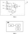
- an optical receiver for receiving optical wireless communication signals, the optical receiver comprises: an optical front-end subsystem according to the present invention; an analog front-end component configured to receive an input signal from the optical front-end subsystem for analog processing; and a modem component configured to implement baseband processing on an output of the analog processed signal from the analog front-end component.
- the disclosed optical front-end subsystem may be coupled with an analog front end and a modem to complete the optical receiver chain. Since only one receiving path is enabled after the selection in the optical front-end subsystem, the analog front end and the modem may be the same as in a convention optical receiver.
- an optical wireless communication system comprises: an optical receiver according to the present invention; an optical transmitter comprising one or more optical front-ends, and wherein each one of the one or more optical front-ends comprises a light source; and wherein the optical receiver is configured to receive optical wireless communication signals transmitted by the optical transmitter.
- the disclosed optical receiver is capable to deal with different transmitter setups, and to provide best receiving capability adaptive to an actual application scenario.
- the transmitter may comprise one or more optical front ends, with each comprising a light source.
- the light source may be one of a light-emitting diode (LED), a laser diode, a vertical-cavity surface-emitting laser (VCSEL), or a hybrid front-end with both LED and VCSEL.
- a method of an optical front-end subsystem for receiving optical wireless communication signals comprises the optical front-end subsystem: receiving, by a first photodiode with a first active surface area, a first optical signal; receiving, by a second photodiode with a second active surface area, a second optical signal; comparing, a received signal strength of the first optical signal with a predefined reference value; and selecting, the received first optical signal as an output signal of the optical front-end subsystem when the received signal strength of the first optical signal is higher than the predefined reference value; and, otherwise, selecting the received second optical signal as the output signal of the optical front-end subsystem; wherein the second active surface area is larger than the first active surface area.
- the method further comprising the optical front-end subsystem: receiving, by a third photodiode with a third active surface area, a third optical signal, and wherein the third active surface area is larger than the first active surface area but smaller than the second active surface area; comparing, a received signal strength of the third optical signal with a predefined third reference value; and selecting the received first optical signal as the output signal of the optical front-end subsystem when the received signal strength of the first optical signal is higher than the predefined reference value; or the received third optical signal as an output signal of the optical front-end subsystem when the received signal strength of the first optical signal is not higher than the predefined reference value and the received signal strength of the third optical signal is higher than the third predefined reference value; or the received second optical signal as the output signal of the optical front-end subsystem when the received signal strength of the first optical signal is not higher than the predefined reference value and the received signal strength of the third optical signal is not higher than the third predefined reference value.
- the invention may further be embodied in a computing program comprising code means which, when the program is executed by an optical front-end subsystem comprising processing means, cause the processing means to perform the method of the optical front-end subsystem as disclosed in the present invention.
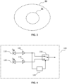
- the optical front-end subsystem 100 comprises a first photodiode 110, a second photodiode 120, a sniffer circuit 140, and a switch 150.
- the first photodiode 110 and the second photodiode 120 may be of the same type or different types of photodiodes.
- photodiodes should be understood in a broad sense, such as photo sensors, light sensors, or photo detectors, which have an active surface area.
- the first photodiode 110 differs from the second photodiode 120 in the size of the active surface area.
- the second active surface area of the second photodiode 120 is larger than the first active surface area of the first photodiode 110.
- different response times are provided by the first photodiode 110 and the second photodiode 120.
- the first photodiode 110 is capable to support higher data rate communication as compared to the second photodiode 120.
- the optical front-end subsystem 100 is configured to make use of the second photodiode to collect energy from the second signal collection area, or a wider FoV as compared to the first signal collection area. Since the active surface area is larger with the second photodiode, the second photodiode is configured to conduct optical receiving for low to medium data rates communication.
- the first photodiode is used to pair with a high-speed narrow beam optical transmitter, such as a VCSEL based optical transmitter.
- the second photodiode is used to pair with a medium to low speed wide beam optical transmitter, such as a LED based optical transmitter.
- a conventional segmented optical receiver more than one uniform photodiode or optical detectors are enabled simultaneously, with each directed to a different orientation and covering a wide FoV in combination.
- the optical receiver may need 4 or more photodiodes.
- each photodiode may have a quite narrow FoV, and then more photodiodes may be needed to cover the entire signal collection area.
- the disclosed system has the advantages on flexibility, low hardware cost, and low power consumption.
- FIG. 2 demonstrates the receiver diversity resulting from different active surface areas of the first photodiode and the second photodiode.
- x-axis represents the distance D between the optical front-end subsystem and an optical transmitter
- y-axis represents the normalized power
- V ref indicates the predefined reference value used as a threshold to compare with the received signal strength of an optical signal.
- x-axis represents the normalized power
- y-axis represents the data rate R to be supported.
- the curves are indicated by 1 st and 2 nd to distinguish between the characteristics between the first photodiode and the second photodiode. From FIG.
- the second photodiode is capable of collecting more energy as compared to the first photodiode, because of its larger active surface area.
- the first photodiode either has a short communication distance or a narrow FoV.
- the first photodiode is capable of supporting higher data rates, because of its smaller junction capacitance and shorter response time. In that sense, the first photodiode is used to cover the application scenarios of relatively short distance but high data rate communication, while the second photodiode is used to cover the application scenarios of relatively longer communication distance but low to medium data rate communication.
- FIG. 4 illustrates another possible system setup of an optical front-end subsystem of the present invention.
- a first amplifier 160 customized to a characteristic of the first photodiode 110 is connected to the first photodiode 110 to amplify the received first optical signal before the first optical signal is assessed by the sniffer circuit 140.
- a second amplifier 170 customized to a characteristic of the second photodiode 120 is connected to the second photodiode 120 to amplify the received second optical signal.
- One or more characteristics or parameters related to an individual photodiode may be considered here, such as the total input capacitance, photodiode signal range, required bandwidth, and required swing with the minimal signal.
- the assessment of the sniffer circuit is based on received optical signal after being conditioned by the amplifier. Because the output electrical signal from a photodiode is typically pretty small, to amplify such small signal from the photodiode to a sufficiently big signal is beneficial for further processing. With the first amplifier 160 dedicated to the first photodiode 110 and the second amplifier 170 dedicated to the second photodiode 120, customized design can be applied to an amplifier considering the properties of a photodiode preceding it. Thus, the optical front-end subsystem is further optimized in the two branches, as compared to the option that another amplified is placed after the switch to process either the received first optical signal or the received second optical signal, depending on the selection being made.
- FIG. 5 illustrates a further possible system setup of an optical front-end subsystem of the present invention.
- a third photodiode 130 is employed, which has a third active surface area larger than the first active surface area of the first photodiode but smaller than the second active surface area of the second photodiode.
- the second active surface area is at least two times of the first active surface area, and the ratio can be as large as 10 times or more.
- the optical front-end subsystem is further enhanced with one more fine-tuned receiving chain to provide a balance between system complexity and the requirements to cover a large variety of application scenarios.
- the optical front-end subsystem may be further extended with a further photodiode, as long as the hardware cost and complexity is justified by the application needs.
- analog front-end component and the modem component may use the same hardware as used in a conventional optical receiver, although the processing capability, such as the bandwidth and clock speed, should be sufficient to process the received signals from either the first photodiode or the second photodiode.
- FIG. 8 shows a flow chart of another implementation of the method 500 of the optical front-end subsystem 100.
- the method 500 comprises the optical front-end subsystem 100 receiving in step S501, by a first photodiode 110 with a first active surface area, a first optical signal; receiving in step S502, by a second photodiode 120 with a second active surface area, a second optical signal. Then, in step S503, the optical front-end subsystem 100 compares a received signal strength of the first optical signal with a predefined reference value.
- the method comprises the optical front-end subsystem 100 receiving, by a third photodiode 130 with a third active surface area, a third optical signal, and wherein the third active surface area is larger than the first active surface area but smaller than the second active surface area.
- the optical front-end subsystem 100 compares, a received signal strength of the third optical signal with a predefined third reference value; and selects in step S507:
- controller is used herein generally to describe various apparatus relating to, among other functions, the operation of one or more network devices or coordinators.
- a controller can be implemented in numerous ways (e.g., such as with dedicated hardware) to perform various functions discussed herein.
- a "processor” is one example of a controller which employs one or more microprocessors that may be programmed using software (e.g., microcode) to perform various functions discussed herein.
- a controller may be implemented with or without employing a processor, and also may be implemented as a combination of dedicated hardware to perform some functions and a processor (e.g., one or more programmed microprocessors and associated circuitry) to perform other functions. Examples of controller components that may be employed in various embodiments of the present disclosure include, but are not limited to, conventional microprocessors, application specific integrated circuits (ASICs), and field-programmable gate arrays (FPGAs).
- ASICs application specific integrated circuits
- FPGAs field-programmable gate arrays
Landscapes
- Engineering & Computer Science (AREA)
- Physics & Mathematics (AREA)
- Electromagnetism (AREA)
- Computer Networks & Wireless Communication (AREA)
- Signal Processing (AREA)
- Computing Systems (AREA)
- Optical Communication System (AREA)
Claims (14)
- Sous-système optique frontal (100) permettant de recevoir des signaux de communication optique sans fil, le sous-système optique frontal (100) comprenant :- une première photodiode (110) avec une première surface active configurée pour recevoir un premier signal optique ;- une deuxième photodiode (120) avec une deuxième surface active configurée pour recevoir un deuxième signal optique ;
le sous-système optique frontal (100) est caractérisé en ce que : le sous-système optique frontal (100) comprenant en outre :- un circuit renifleur (140) configuré pour comparer une intensité de signal reçu du premier signal optique à une valeur de référence prédéfinie ; et- un commutateur (150) configuré pour sélectionner le premier signal optique reçu en tant que signal de sortie du sous-système optique frontal (100) lorsque l'intensité de signal reçu du premier signal optique est supérieure à la valeur de référence prédéfinie ; et, sinon, sélectionner le deuxième signal optique reçu en tant que signal de sortie du sous-système optique frontal (100) ;
dans lequel la deuxième surface active est plus grande que la première surface active. - Sous-système optique frontal (100) selon la revendication 1, dans lequel la deuxième surface active est au moins deux fois supérieure à la première surface active.
- Sous-système optique frontal (100) selon la revendication 1 ou 2, dans lequel la première photodiode (110) est en outre configurée pour recevoir le premier signal optique dans une première zone de collecte de signaux (Z1) et la deuxième photodiode (120) est en outre configurée pour recevoir le deuxième signal optique dans une seconde zone de collecte de signaux (Z2), et la seconde zone de collecte de signaux (Z2) est plus grande que la première zone de collecte de signaux (Z1).
- Sous-système optique frontal (100) selon l'une quelconque des revendications précédentes, dans lequel la première zone de collecte de signaux (Z1) est entièrement couverte par la seconde zone de collecte de signaux (Z2).
- Sous-système optique frontal (100) selon l'une quelconque des revendications précédentes, dans lequel la première photodiode (110) est configurée pour prendre en charge un débit de données plus élevé que la deuxième photodiode (120).
- Sous-système optique frontal (100) selon l'une quelconque des revendications précédentes, dans lequel le circuit renifleur (140) comprend en outre un détecteur de valeur quadratique moyenne, RMS, configuré pour estimer une intensité de signal reçu.
- Sous-système optique frontal (100) selon l'une quelconque des revendications précédentes, le sous-système optique frontal (100) comprend en outre :- un premier amplificateur (160) connecté à la première photodiode (110) et configuré pour amplifier le premier signal optique reçu à l'aide d'un premier circuit amplificateur personnalisé pour une caractéristique de la première photodiode (110) ; et- un deuxième amplificateur (170), connecté à la deuxième photodiode (120), configuré pour amplifier le deuxième signal optique reçu à l'aide d'un second circuit amplificateur personnalisé pour une caractéristique de la deuxième photodiode (120) ; et
dans lequel le circuit renifleur (140) est en outre configuré pour comparer l'intensité de signal reçu du premier signal optique à une seconde valeur de référence prédéfinie, après que le premier signal optique est amplifié par le premier amplificateur (160). - Sous-système optique frontal (100) selon la revendication 7, dans lequel le premier amplificateur (160) et/ou le deuxième amplificateur (170) est un amplificateur transimpédance, TIA.
- Sous-système optique frontal (100) selon l'une quelconque des revendications précédentes, le sous-système optique frontal (100) comprenant en outre :- une troisième photodiode (130) avec une troisième surface active configurée pour recevoir un troisième signal optique, et dans lequel la troisième surface active est plus grande que la première surface active mais plus petite que la deuxième surface active ; etdans lequel le circuit renifleur (140) est en outre configuré pour :- comparer une intensité de signal reçu du troisième signal optique à une troisième valeur de référence prédéfinie ; etla commutation (150) est en outre configurée pour :- sélectionner le premier signal optique reçu en tant que signal de sortie du sous-système optique frontal (100) lorsque l'intensité de signal reçu du premier signal optique est supérieure à la valeur de référence prédéfinie ; et, pour sélectionner le troisième signal optique reçu en tant que signal de sortie du sous-système optique frontal (100) lorsque l'intensité de signal reçu du premier signal optique n'est pas supérieure à la valeur de référence prédéfinie et que l'intensité de signal reçu du troisième signal optique est supérieure à la troisième valeur de référence prédéfinie ; et, sinon, sélectionner le deuxième signal optique reçu en tant que signal de sortie du sous-système optique frontal (100).
- Récepteur optique (200) permettant de recevoir des signaux de communication optique sans fil, le récepteur optique comprenant :- un sous-système optique frontal (100) selon l'une quelconque des précédentes revendications 1 à 9 ;- un composant analogique frontal (210) configuré pour recevoir un signal d'entrée provenant du sous-système optique frontal (100) pour un traitement analogique ; et- un composant modem (220) configuré pour mettre en oeuvre un traitement de bande de base sur une sortie du signal traité analogique provenant du composant analogique frontal (210).
- Système de communication optique sans-fil, le système de communication optique sans fil comprenant :- un récepteur optique (200) selon la revendication 10 ;- un émetteur optique comprenant une ou plusieurs extrémités avant optiques, et dans lequel chacune de la ou des extrémités avant optiques comprend une source de lumière ;
et dans lequel le récepteur optique est configuré pour recevoir des signaux de communication optique sans fil transmis par l'émetteur optique. - Procédé (500) selon un sous-système optique frontal (100) permettant de recevoir des signaux de communication optique sans fil, le procédé comprenant le sous-système optique frontal (100) :- la réception (S501), par une première photodiode (110) avec une première surface active, un premier signal optique ;- la réception (S502), par une deuxième photodiode (120) avec une deuxième surface active, un deuxième signal optique ;
le procédé (500) est caractérisé en ce que :
le procédé (500) comprenant en outre le sous-système optique frontal (100) :- la comparaison (S503) d'une intensité de signal reçu du premier signal optique avec une valeur de référence prédéfinie ; et- la sélection (S504), du premier signal optique reçu en tant que signal de sortie du sous-système optique frontal lorsque l'intensité de signal reçu du premier signal optique est supérieure à la valeur de référence prédéfinie ; et, sinon, la sélection du deuxième signal optique reçu en tant que signal de sortie du sous-système optique frontal ;
dans lequel la deuxième surface active est plus grande que la première surface active. - Procédé (500) selon la revendication 12, le procédé (500) comprenant en outre le sous-système optique frontal (100) :- la réception (S505), par une troisième photodiode (130) avec une troisième surface active, d'un troisième signal optique, et dans lequel la troisième surface active est plus grande que la première surface active mais plus petite que la deuxième surface active ;- la comparaison (S506) d'une intensité de signal reçu du troisième signal optique à une troisième valeur de référence prédéfinie ; et- la sélection (S507)o du premier signal optique reçu en tant que signal de sortie du sous-système optique frontal lorsque l'intensité de signal reçu du premier signal optique est supérieure à la valeur de référence prédéfinie ; ouo du troisième signal optique reçu en tant que signal de sortie du sous-système optique frontal lorsque l'intensité de signal reçu du premier signal optique n'est pas supérieure à la valeur de référence prédéfinie et que l'intensité de signal reçu du troisième signal optique est supérieure à la troisième valeur de référence prédéfinie ; ouo du deuxième signal optique reçu en tant que signal de sortie du sous-système optique frontal lorsque l'intensité de signal reçu du premier signal optique n'est pas supérieure à la valeur de référence prédéfinie et que l'intensité de signal reçu du troisième signal optique n'est pas supérieure à la troisième valeur de référence prédéfinie.
- Programme informatique comprenant un moyen de code qui, lorsque le programme est exécuté par un moyen de traitement de signal du sous-système optique frontal (100) selon les revendications 1 à 9, amène le sous-système optique frontal à mettre en oeuvre l'un quelconque des procédés selon les revendications 12 à 13.
Applications Claiming Priority (2)
| Application Number | Priority Date | Filing Date | Title |
|---|---|---|---|
| EP20189817 | 2020-08-06 | ||
| PCT/EP2021/070326 WO2022028888A1 (fr) | 2020-08-06 | 2021-07-21 | Système de réception pour communication sans fil optique à grande vitesse et à grande couverture |
Publications (2)
| Publication Number | Publication Date |
|---|---|
| EP4193493A1 EP4193493A1 (fr) | 2023-06-14 |
| EP4193493B1 true EP4193493B1 (fr) | 2023-12-13 |
Family
ID=71994365
Family Applications (1)
| Application Number | Title | Priority Date | Filing Date |
|---|---|---|---|
| EP21748568.9A Active EP4193493B1 (fr) | 2020-08-06 | 2021-07-21 | Système de réception de communication optique sans fil haut débit et à grande couverture |
Country Status (5)
| Country | Link |
|---|---|
| US (1) | US20230283374A1 (fr) |
| EP (1) | EP4193493B1 (fr) |
| JP (1) | JP7413605B2 (fr) |
| CN (1) | CN116097584A (fr) |
| WO (1) | WO2022028888A1 (fr) |
Family Cites Families (6)
| Publication number | Priority date | Publication date | Assignee | Title |
|---|---|---|---|---|
| JP4704206B2 (ja) | 2004-12-21 | 2011-06-15 | パナソニック株式会社 | 光受信器 |
| JP2007135144A (ja) | 2005-11-14 | 2007-05-31 | Shimizu Corp | 可視光通信用受信装置 |
| US7929865B2 (en) * | 2007-07-27 | 2011-04-19 | Hewlett-Packard Development Company, L.P. | Free space WDM signal detector |
| JP2011135206A (ja) | 2009-12-22 | 2011-07-07 | Panasonic Corp | 光ワイヤレス通信装置 |
| JP2017055375A (ja) | 2015-09-10 | 2017-03-16 | 住友電工システムソリューション株式会社 | 光ビーコン |
| JP2018129095A (ja) | 2018-05-10 | 2018-08-16 | 住友電気工業株式会社 | 光ビーコン及び車載機 |
-
2021
- 2021-07-21 JP JP2023507828A patent/JP7413605B2/ja active Active
- 2021-07-21 US US18/019,476 patent/US20230283374A1/en active Pending
- 2021-07-21 EP EP21748568.9A patent/EP4193493B1/fr active Active
- 2021-07-21 WO PCT/EP2021/070326 patent/WO2022028888A1/fr active Application Filing
- 2021-07-21 CN CN202180057101.0A patent/CN116097584A/zh active Pending
Also Published As
| Publication number | Publication date |
|---|---|
| JP2023532146A (ja) | 2023-07-26 |
| CN116097584A (zh) | 2023-05-09 |
| US20230283374A1 (en) | 2023-09-07 |
| EP4193493A1 (fr) | 2023-06-14 |
| JP7413605B2 (ja) | 2024-01-15 |
| WO2022028888A1 (fr) | 2022-02-10 |
Similar Documents
| Publication | Publication Date | Title |
|---|---|---|
| US10680719B2 (en) | Electronic device associated with a photovoltaic module to optimise the throughput of a bidirectional VLC transmission | |
| Jenila et al. | Green indoor optical wireless communication systems: Pathway towards pervasive deployment | |
| JP2001292107A (ja) | 受信装置、送信装置、および通信システム | |
| US11750284B2 (en) | Optical wireless communication system and method | |
| US20230361874A1 (en) | Receiver and associated mobile communications device | |
| US20200136724A1 (en) | Conformal visible light communication (vlc) receiver and method of use | |
| Ali et al. | Giga-bit Transmission between an Eye-safe transmitter and wide field-of-view SiPM receiver | |
| EP4193493B1 (fr) | Système de réception de communication optique sans fil haut débit et à grande couverture | |
| Soltani et al. | Terabit indoor laser-based wireless communications: LiFi 2.0 for 6G | |
| US10187146B2 (en) | Light converting device | |
| WO2022048845A1 (fr) | Système de réception pour communication sans fil optique à grande vitesse et à grande couverture | |
| Azarkh et al. | Optimal detector size for optical wireless communication links with wide coverage | |
| KR102211484B1 (ko) | 무선 광통신에서 배경 광 잡음의 완화를 위한 공간 선택적 신호 수신 장치 및 방법 | |
| Alqudah et al. | Optical wireless multispot diffusing: a MIMO configuration | |
| US20240022325A1 (en) | A hybrid optical transmitter for high speed optical wireless communication | |
| EP4005113A1 (fr) | Système et procédé de transferts intercellulaires dans un réseau de communications sans fil optique | |
| Singh et al. | Performance Evaluation of Visible Light Communication System based on Optical Power Distribution with Channel Delay Spread and SNR | |
| Vaishali et al. | Lambertian Luminous Intensity Radiation Pattern Analysis in OLOS Indoor Propagation for Better Connectivity | |
| Olaluyi et al. | Investigation of Visible Light Communication in an Indoor Environment: A Case Study of Afe Babalola University’s Communication Laboratory | |
| US11177882B2 (en) | Receiver for low-power optical signals with operation in conditions of high incidence of background light and application in visible light communication | |
| KR102018216B1 (ko) | 가시광 통신용 수신장치 | |
| WO2022243229A1 (fr) | Technique de sectorisation pour communication sans fil optique à grande vitesse | |
| Liu et al. | Wireless Laser Uplink Scheme with 1550-Nm Wavelength for Indoor Visible Light Communications | |
| Han et al. | Optical Spectrum Estimation Technique for Optical Interference Cancellation in High Speed Transmission MISO-OCVLC Environment | |
| Shorna et al. | Performance Analysis of spot diffusion technique for indoor optical communication system employing LDPC |
Legal Events
| Date | Code | Title | Description |
|---|---|---|---|
| STAA | Information on the status of an ep patent application or granted ep patent |
Free format text: STATUS: UNKNOWN |
|
| STAA | Information on the status of an ep patent application or granted ep patent |
Free format text: STATUS: THE INTERNATIONAL PUBLICATION HAS BEEN MADE |
|
| PUAI | Public reference made under article 153(3) epc to a published international application that has entered the european phase |
Free format text: ORIGINAL CODE: 0009012 |
|
| STAA | Information on the status of an ep patent application or granted ep patent |
Free format text: STATUS: REQUEST FOR EXAMINATION WAS MADE |
|
| 17P | Request for examination filed |
Effective date: 20230306 |
|
| AK | Designated contracting states |
Kind code of ref document: A1 Designated state(s): AL AT BE BG CH CY CZ DE DK EE ES FI FR GB GR HR HU IE IS IT LI LT LU LV MC MK MT NL NO PL PT RO RS SE SI SK SM TR |
|
| DAV | Request for validation of the european patent (deleted) | ||
| DAX | Request for extension of the european patent (deleted) | ||
| GRAP | Despatch of communication of intention to grant a patent |
Free format text: ORIGINAL CODE: EPIDOSNIGR1 |
|
| STAA | Information on the status of an ep patent application or granted ep patent |
Free format text: STATUS: GRANT OF PATENT IS INTENDED |
|
| INTG | Intention to grant announced |
Effective date: 20230706 |
|
| GRAS | Grant fee paid |
Free format text: ORIGINAL CODE: EPIDOSNIGR3 |
|
| GRAA | (expected) grant |
Free format text: ORIGINAL CODE: 0009210 |
|
| STAA | Information on the status of an ep patent application or granted ep patent |
Free format text: STATUS: THE PATENT HAS BEEN GRANTED |
|
| AK | Designated contracting states |
Kind code of ref document: B1 Designated state(s): AL AT BE BG CH CY CZ DE DK EE ES FI FR GB GR HR HU IE IS IT LI LT LU LV MC MK MT NL NO PL PT RO RS SE SI SK SM TR |
|
| P01 | Opt-out of the competence of the unified patent court (upc) registered |
Effective date: 20231102 |
|
| REG | Reference to a national code |
Ref country code: GB Ref legal event code: FG4D |
|
| REG | Reference to a national code |
Ref country code: CH Ref legal event code: EP |
|
| REG | Reference to a national code |
Ref country code: DE Ref legal event code: R096 Ref document number: 602021007731 Country of ref document: DE |
|
| REG | Reference to a national code |
Ref country code: IE Ref legal event code: FG4D |
|
| PG25 | Lapsed in a contracting state [announced via postgrant information from national office to epo] |
Ref country code: GR Free format text: LAPSE BECAUSE OF FAILURE TO SUBMIT A TRANSLATION OF THE DESCRIPTION OR TO PAY THE FEE WITHIN THE PRESCRIBED TIME-LIMIT Effective date: 20240314 |
|
| REG | Reference to a national code |
Ref country code: LT Ref legal event code: MG9D |
|
| PG25 | Lapsed in a contracting state [announced via postgrant information from national office to epo] |
Ref country code: LT Free format text: LAPSE BECAUSE OF FAILURE TO SUBMIT A TRANSLATION OF THE DESCRIPTION OR TO PAY THE FEE WITHIN THE PRESCRIBED TIME-LIMIT Effective date: 20231213 |
|
| REG | Reference to a national code |
Ref country code: NL Ref legal event code: MP Effective date: 20231213 |
|
| PG25 | Lapsed in a contracting state [announced via postgrant information from national office to epo] |
Ref country code: ES Free format text: LAPSE BECAUSE OF FAILURE TO SUBMIT A TRANSLATION OF THE DESCRIPTION OR TO PAY THE FEE WITHIN THE PRESCRIBED TIME-LIMIT Effective date: 20231213 |
|
| PG25 | Lapsed in a contracting state [announced via postgrant information from national office to epo] |
Ref country code: LT Free format text: LAPSE BECAUSE OF FAILURE TO SUBMIT A TRANSLATION OF THE DESCRIPTION OR TO PAY THE FEE WITHIN THE PRESCRIBED TIME-LIMIT Effective date: 20231213 Ref country code: GR Free format text: LAPSE BECAUSE OF FAILURE TO SUBMIT A TRANSLATION OF THE DESCRIPTION OR TO PAY THE FEE WITHIN THE PRESCRIBED TIME-LIMIT Effective date: 20240314 Ref country code: ES Free format text: LAPSE BECAUSE OF FAILURE TO SUBMIT A TRANSLATION OF THE DESCRIPTION OR TO PAY THE FEE WITHIN THE PRESCRIBED TIME-LIMIT Effective date: 20231213 Ref country code: BG Free format text: LAPSE BECAUSE OF FAILURE TO SUBMIT A TRANSLATION OF THE DESCRIPTION OR TO PAY THE FEE WITHIN THE PRESCRIBED TIME-LIMIT Effective date: 20240313 |