EP4192002A1 - Procédé de génération d'un filtre de désentrelacement et appareil de traitement d'images - Google Patents
Procédé de génération d'un filtre de désentrelacement et appareil de traitement d'images Download PDFInfo
- Publication number
- EP4192002A1 EP4192002A1 EP21212245.1A EP21212245A EP4192002A1 EP 4192002 A1 EP4192002 A1 EP 4192002A1 EP 21212245 A EP21212245 A EP 21212245A EP 4192002 A1 EP4192002 A1 EP 4192002A1
- Authority
- EP
- European Patent Office
- Prior art keywords
- pixels
- interlacing
- representation
- spatial frequency
- frequency domain
- Prior art date
- Legal status (The legal status is an assumption and is not a legal conclusion. Google has not performed a legal analysis and makes no representation as to the accuracy of the status listed.)
- Pending
Links
Images




Classifications
-
- H—ELECTRICITY
- H04—ELECTRIC COMMUNICATION TECHNIQUE
- H04N—PICTORIAL COMMUNICATION, e.g. TELEVISION
- H04N23/00—Cameras or camera modules comprising electronic image sensors; Control thereof
- H04N23/60—Control of cameras or camera modules
- H04N23/68—Control of cameras or camera modules for stable pick-up of the scene, e.g. compensating for camera body vibrations
- H04N23/682—Vibration or motion blur correction
- H04N23/683—Vibration or motion blur correction performed by a processor, e.g. controlling the readout of an image memory
-
- G—PHYSICS
- G06—COMPUTING OR CALCULATING; COUNTING
- G06T—IMAGE DATA PROCESSING OR GENERATION, IN GENERAL
- G06T5/00—Image enhancement or restoration
- G06T5/73—Deblurring; Sharpening
-
- G—PHYSICS
- G06—COMPUTING OR CALCULATING; COUNTING
- G06T—IMAGE DATA PROCESSING OR GENERATION, IN GENERAL
- G06T5/00—Image enhancement or restoration
- G06T5/10—Image enhancement or restoration using non-spatial domain filtering
-
- G—PHYSICS
- G06—COMPUTING OR CALCULATING; COUNTING
- G06T—IMAGE DATA PROCESSING OR GENERATION, IN GENERAL
- G06T5/00—Image enhancement or restoration
- G06T5/20—Image enhancement or restoration using local operators
-
- G—PHYSICS
- G06—COMPUTING OR CALCULATING; COUNTING
- G06T—IMAGE DATA PROCESSING OR GENERATION, IN GENERAL
- G06T5/00—Image enhancement or restoration
- G06T5/70—Denoising; Smoothing
-
- G—PHYSICS
- G06—COMPUTING OR CALCULATING; COUNTING
- G06T—IMAGE DATA PROCESSING OR GENERATION, IN GENERAL
- G06T7/00—Image analysis
- G06T7/10—Segmentation; Edge detection
- G06T7/168—Segmentation; Edge detection involving transform domain methods
-
- H—ELECTRICITY
- H04—ELECTRIC COMMUNICATION TECHNIQUE
- H04N—PICTORIAL COMMUNICATION, e.g. TELEVISION
- H04N23/00—Cameras or camera modules comprising electronic image sensors; Control thereof
- H04N23/20—Cameras or camera modules comprising electronic image sensors; Control thereof for generating image signals from infrared radiation only
- H04N23/23—Cameras or camera modules comprising electronic image sensors; Control thereof for generating image signals from infrared radiation only from thermal infrared radiation
-
- H—ELECTRICITY
- H04—ELECTRIC COMMUNICATION TECHNIQUE
- H04N—PICTORIAL COMMUNICATION, e.g. TELEVISION
- H04N23/00—Cameras or camera modules comprising electronic image sensors; Control thereof
- H04N23/80—Camera processing pipelines; Components thereof
- H04N23/81—Camera processing pipelines; Components thereof for suppressing or minimising disturbance in the image signal generation
-
- G—PHYSICS
- G06—COMPUTING OR CALCULATING; COUNTING
- G06T—IMAGE DATA PROCESSING OR GENERATION, IN GENERAL
- G06T2207/00—Indexing scheme for image analysis or image enhancement
- G06T2207/10—Image acquisition modality
- G06T2207/10048—Infrared image
-
- G—PHYSICS
- G06—COMPUTING OR CALCULATING; COUNTING
- G06T—IMAGE DATA PROCESSING OR GENERATION, IN GENERAL
- G06T2207/00—Indexing scheme for image analysis or image enhancement
- G06T2207/20—Special algorithmic details
- G06T2207/20021—Dividing image into blocks, subimages or windows
-
- G—PHYSICS
- G06—COMPUTING OR CALCULATING; COUNTING
- G06T—IMAGE DATA PROCESSING OR GENERATION, IN GENERAL
- G06T2207/00—Indexing scheme for image analysis or image enhancement
- G06T2207/20—Special algorithmic details
- G06T2207/20048—Transform domain processing
- G06T2207/20056—Discrete and fast Fourier transform, [DFT, FFT]
-
- G—PHYSICS
- G06—COMPUTING OR CALCULATING; COUNTING
- G06T—IMAGE DATA PROCESSING OR GENERATION, IN GENERAL
- G06T2207/00—Indexing scheme for image analysis or image enhancement
- G06T2207/20—Special algorithmic details
- G06T2207/20172—Image enhancement details
- G06T2207/20201—Motion blur correction
-
- H—ELECTRICITY
- H04—ELECTRIC COMMUNICATION TECHNIQUE
- H04N—PICTORIAL COMMUNICATION, e.g. TELEVISION
- H04N25/00—Circuitry of solid-state image sensors [SSIS]; Control thereof
- H04N25/40—Extracting pixel data from image sensors by controlling scanning circuits, e.g. by modifying the number of pixels sampled or to be sampled
Definitions
- the present invention relates to method of generating a de-interlacing filter, the method being of the type that, for example, is applied to an image to remove motion artefacts.
- the present invention also relates to an image processing apparatus of the type that, for example, processes an image to remove motion artefacts.
- Video interlacing is a known technique to reduce transmission bandwidth requirements for frames of video content.
- a video frame is divided into multiple subframes, for example two subframes.
- Each subframe occurs consecutively in a repeating alternating pattern, for example: subframe 1 - subframe 2 - subframe 1 - subframe 2, - ....
- the effect of dividing the video frame is, for example, to halve the bandwidth required to transmit the video frame and hence video content.
- the MLX90640 far infra-red thermal sensor array available from Melexis Technologies NV supports two subframes, because the readout circuit of the sensor array is shared between two sets of detector cells. In operation, measurements in respect of a first set of detector cells are made during a first subframe and then measurements in respect of a second set of detector cells are made during a second subsequent subframe following immediately after the first subframe. Hence, a full measurement frame of the sensor array is updated at a speed of half the refresh rate.
- a default arrangement for reading the detector cells of the sensor array is a chequerboard pattern, whereby detector cells of a first logical "colour" are read during the first subframe and detector cells of a second logical "colour" are read during the second subframe.
- This manner of reading the detector cells is known as interlaced scanning and is susceptible to so-called motion artifacts, also known as interlacing effects.
- the motion artifacts appear when an object being captured in the field of view of the sensor array moves sufficiently fast so as to be in different spatial positions during each subframe when the respective sets of detector cells are being read, i.e. the moving object is imaged onto a different sets of detector cells between subframes.
- a method of generating a de-interlacing filter comprising: analysing a pixel array comprising an interlacing pattern of pixels, the interlacing pattern of pixels comprising a first plurality of pixels and a second plurality of pixels configured to be read during a first measurement subframe and a second measurement subframe of a plurality of measurement subframes, respectively; generating an n-state representation of the interlacing pattern of pixels distinguishing between the first plurality of pixels and the second plurality of pixels, where n is the number of measurement subframes; translating the n-state representation of the interlacing pattern to a spatial frequency domain, thereby generating a spatial frequency domain representation of the n-state representation of the interlacing pattern; removing a DC signal component from the spatial frequency domain representation of the n-state representation of the interlacing pattern, thereby generating a DC-less spatial frequency domain representation; selecting a kernel filter configured to blur; and convolving the DC-less spatial frequency
- the first and second measurement subframes may relate to different time intervals within a measurement time frame.
- the first and second measurement subframes may be consecutive.
- the first and second measurement subframes may be non-overlapping.
- the kernel filter may be a Gaussian blur filter or a box blur filter.
- the interlacing pattern may be a chequerboard pattern.
- the interlacing pattern may be an interleaved pattern.
- the interleaved pattern may comprise a series of alternating horizontal lines of pixels.
- the interlacing pattern of pixels may comprise a third plurality of pixels to be read in respect of a third measurement subframe; the n-state representation of the interlacing pattern of pixels may distinguish between the first plurality of pixels, the second plurality of pixels, and the third plurality of pixels.
- Translating the n-state representation of the interlacing pattern to the spatial frequency domain may comprise: calculating a two-dimensional Fourier transform in respect of the n-state representation of the interlacing pattern.
- Generating the n-state representation of the interlacing pattern of pixels may comprise: generating a measurement subframe map of the pixel array; the measurement subframe map may be an array representing each pixel of the pixel array; and for each element of the measurement subframe map, recording the measurement subframe assigned to the corresponding pixel of the pixel array.
- the plurality of measurement subframes may be two measurement subframes.
- the plurality of measurement subframes may be three measurement subframes.
- a method of de-interlacing an image comprising: capturing an image; translating the image to the spatial frequency domain; generating a de-interlacing filter as set forth above in relation to the first aspect of the present invention; and applying the de-interlacing filter to the spatial frequency domain representation of the image captured.
- the de-interlacing filter may be applied by multiplying the de-interlacing filter with the frequency domain representation of the image captured, thereby generating a de-interlaced image in the spatial frequency domain.
- the method may further comprise: translating the de-interlaced image in the spatial frequency domain to the spatial domain.
- the image captured may be a thermal image.
- an image processing apparatus comprising: a pixel array configured to receive electromagnetic radiation and measure electrical signals generated by each pixel of the pixel array in response to receipt of the electromagnetic radiation, the pixel array comprising an interlacing pattern of pixels, the interlacing pattern of pixels comprising a first plurality of pixels and a second plurality of pixels configured to be read during a first measurement subframe and a second measurement subframe of a plurality of measurement subframes, respectively; and a signal processing circuit configured to analyse the pixel array and to generate an n-state representation of the interlacing pattern of pixels distinguishing between the first plurality of pixels and the second plurality of pixels, where n is the number of measurement subframes; wherein the signal processing circuit is configured to translate the n-state representation of the interlacing pattern to a spatial frequency domain, thereby generating a spatial frequency domain representation of the n-state representation of the interlacing pattern; the signal processing circuit is configured to remove a DC signal component from the spatial frequency domain representation of the
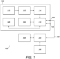
- an imaging system for example a temperature imaging system 100, comprises a far infra-red thermal sensor array 102, for example an MLX90640 sensor available from Melexis Technologies NV, the thermal sensor array 102 being operably coupled to a processing resource 104, for example a microcontroller, constituting a signal processing circuit.
- the processing resource 104 is operably coupled to a digital memory 106 and an input/output (I/O) interface 108.
- the I/O interface 108 can be operably coupled to a display (not shown) for providing a visual representation of the measurements made by the thermal sensor array 102 and an input device (not shown) for receiving control information, for example setting parameters, and triggering measurement.
- the thermal sensor array 102 comprises an array of M pixels 110, for example an array of 32 x 24 pixels, the array of sensors 102 being operably coupled to an array of M amplifiers 112.
- the array of M amplifiers 112 is operably coupled to an array of M Analogue-to-Digital Converters (ADCs) 114, the array of M ADCs 114 being operably coupled to an Inter-Integrated Circuit (I 2 C) unit 116 in order to support communications between the thermal sensor array 102 and the processing resource 104.
- a serial data port 118 of the I 2 C unit 116 is therefore operably coupled to the processing resource 104 via a serial data line 120.
- the I 2 C unit 116 also has a clock input 122 for receiving a clock signal in common with the processing resource 104 for communications purposes.
- the I 2 C unit 116 is also operably coupled to a volatile memory, for example a Random Access Memory (RAM) 124 and a non-volatile memory, for example an Electronically Erasable Programmable Read Only Memory (EEPROM) 126.
- RAM Random Access Memory
- EEPROM Electronically Erasable Programmable Read Only Memory
- the array of M pixels 110 of the thermal sensor array 102 of Figure 1 comprises a first set of pixels and a second set of pixels that respectively share the array of M amplifiers 112 and the array of M ADCs 114 in accordance with a first interlacing scan sequence.
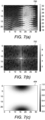
- the first interlacing scan sequence has a first interlacing pixel pattern 300 ( Figure 3(a) ) associated therewith, the first interlacing scan sequence employing a first interlacing subframe and a second interlacing subframe within a measurement subframe.
- a de-interlacing filter can be generated on-the-fly or can be pre-generated and stored in the digital memory 106 for repeated use.
- the processing resource 104 analyses the first interlacing pixel pattern 300 in order to generate (Step 200) a digital representation of the first interlacing pixel pattern 300, for example using a binary representation for each pixel according to the interlacing subframe to which the pixel relates.
- a digital representation of the first interlacing pixel pattern 300 for example using a binary representation for each pixel according to the interlacing subframe to which the pixel relates.
- the first interlacing scan sequence employs two subframes, two distinct values are used to designate spatially the subframes to which each pixel relates, the positional information associated with each pixel and subframe being recorded in an array data structure, for example.
- the digital representation of the first interlacing pixel pattern 300 constitutes a map of the pixel array distinguishing pixels assigned to different subframes and hence designates a subframe of the interlacing pixel scan sequence to which each pixel of the array of M pixels 110 relates. More generally, the interlacing pixel pattern comprises a first plurality of pixels and a second plurality of pixels configured to be read during a first measurement subframe and a second measurement subframe of a plurality of measurement subframes, respectively, each of the first and second measurement subframes corresponding to a different period of time within a measurement time frame. In this example, the first and second measurement subframes alternate over a plurality of measurement frames.
- an n-state representation of the interlacing pixel pattern is generated and distinguishes between the first plurality of pixels and the second plurality of pixels, where n is the number of measurement subframes.
- n is the number of measurement subframes.
- two distinct values are employed to distinguish between pixels relating to the first measurement subframe and the second measurement subframe.
- n-bit binary numbers can be employed to represent respectively each measurement subframe.
- the processing resource 104 generates (Step 202) a two-dimensional Fast Fourier Transform (FFT) of the digital representation of the first interlacing pixel pattern 300 to yield a first 2D FFT representation 302 ( Figure 3(b) ) constituting a spatial frequency domain representation of the n-state representation of the first interlacing pixel pattern 300.
- FFT Fast Fourier Transform
- the spatial frequency of images is defined as the number of lines per millimeter.
- abrupt changes in temperature between two neighboring pixels for example as caused by a moving object in the field of view of the thermal sensor array 102, leads to high frequency components in the spatial frequency domain.
- the highest frequencies associated with the motion artefacts are located in the corners of the first 2D FFT binary representation 302.
- the first 2D FFT binary representation 302 also comprises a DC component, but the de-interlacing filter only has to remove the high frequency components and so it is necessary to remove (Step 204) the DC component from the first 2D FFT binary representation 302 when generating the de-interlacing filter, the DC component being located in the centre of the first 2D FFT binary representation 302. Following removal of the DC component, a first DC-less 2D FFT binary representation results, constituting a DC-less spatial frequency domain representation.
- a kernel filter configured to blur can be selected and applied, by convolution, to the first DC-less 2D FFT binary representation in order to include those frequencies in the interlacing filter that is being generated.
- the blurring kernel is a Gaussian kernel, but other suitable kernels can be employed depending upon the distribution of the high-frequency components in the first 2D FFT binary representation 302.
- the Gaussian kernel is particularly suited owing to frequencies of the first 2D FFT binary representation 302 being evenly distributed in x and y directions.
- other blur filters can be employed, for example a box blur filter.
- the processing resource 104 therefore applies (Step 206) the Gaussian blurring kernel by convolution to the first DC-less 2D FFT binary representation to yield the de-interlacing filter 304 ( Figure 3(c) ).
- the convolution is achieved by generating an FFT of the kernel filter and multiplying the FFT of the kernel filter with the first DC-less 2D FFT binary representation.
- a second interlacing scan sequence is employed instead of the first interlacing scan sequence.
- the second interlacing scan sequence employs a second interlacing pixel pattern 400 ( Figure 4(a) ), which the processing resource 104 analyses in order to generate (Step 200) a digital representation of the second interlacing pixel pattern 400, for example using a binary representation for each pixel according to the interlacing subframe to which the pixel relates, as in the example of the first interlacing pixel pattern 300 described above.
- the processing resource 104 generates (Step 202) a two-dimensional Fast Fourier Transform (FFT) of the digital representation of the second interlacing pixel pattern 400 to yield a second 2D FFT binary representation 402 ( Figure 4(b) ).
- FFT Fast Fourier Transform
- the second interlacing scan sequence which employs an alternating horizontal line pattern constituting an example of an interleaved pattern
- the highest frequencies associated with the motion artefacts are now located centrally in the upper and lower regions of the second 2D FFT binary representation 402.
- the second 2D FFT binary representation 402 again also comprises a DC component, but the de-interlacing filter only has to remove the high frequency components and so it is necessary to remove (Step 204) the DC component from the second 2D FFT binary representation 402 when generating the de-interlacing filter, the DC component being again located in the centre of the second 2D FFT binary representation 402. Following removal of the DC component, a second DC-less 2D FFT binary representation results.
- a blurring kernel can again be applied, by convolution, to the second DC-less 2D FFT binary representation in order to include, in the interlacing filter that is being generated, frequencies around the locations of the high frequencies in the second DC-less 2D FFT binary representation.
- the blurring kernel is a Gaussian kernel, but other suitable kernels can be employed depending upon the distribution of the high-frequency components in the second 2D FFT binary representation 402.
- the processing resource 104 therefore applies (Step 206) the Gaussian blurring kernel to the second DC-less 2D FFT binary representation to yield the second de-interlacing filter 404 ( Figure 4(c) ).
- an image captured by the temperature imaging system 100 is de-interlaced as follows. Electromagnetic radiation emitted by an object is received by the array of M pixels 110 and electrical signals are generated in response to the received electromagnetic radiation and measured by the thermal sensor array 102.
- the temperature imaging system 100 thus initially captures (Step 500) a first image 600 ( Figure 6(a) ). Thereafter, the processing resource 104 generates (Step 502) a first 2D FFT of the captured image 602 ( Figure 6(b) ), thereby translating the first image 600 to the spatial frequency domain, as well as generating (Step 504) the first de-interlacing filter 304 ( Figure 6(c) ).
- the first de-interlacing filter 304 is in the spatial frequency domain, as of course is the first 2D FFT of the captured image 602.
- the first 2D FFT of the captured image 602 is then convolved with the first de-interlacing filter 304, but as both are in the spatial frequency domain, the convolution is achieved by simple multiplication (Step 506) of the first 2D FFT of the captured image 602 with the first de-interlacing filter 304 to yield a first frequency domain filtered image 604 ( Figure 6(d) ) in the spatial frequency domain.
- the first frequency domain filtered image 604 is converted back to the spatial domain by performing an inverse FFT on the first frequency domain filtered image 604 to yield a first de-interlaced image 606 ( Figure 6(e) ).
- an image is again captured by the temperature imaging system 100 and de-interlaced as follows.
- the temperature imaging system 100 initially captures (Step 500) a second image 700 ( Figure 7(a) ). Thereafter, the processing resource 104 generates (Step 502) a second 2D FFT of the captured image 702 ( Figure 7(b) ) as well as generating (Step 504) the second de-interlacing filter 404 ( Figure 7(c) ).
- the second de-interlacing filter 404 is in the spatial frequency domain, as of course is the second 2D FFT of the captured image 702.
- the second 2D FFT of the captured image 702 is then convolved with the second de-interlacing filter 404, but as both are in the spatial frequency domain, the convolution is achieved by simple multiplication (Step 506) of the second 2D FFT of the captured image 702 with the second de-interlacing filter 404 to yield a second frequency domain filtered image 704 ( Figure 7(d) ).
- the second frequency domain filtered image 704 is converted back to the spatial domain by performing an inverse FFT on the second frequency domain filtered image 704 to yield a second de-interlaced image 706 ( Figure 6(c) ).
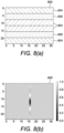
- the third interlacing pattern 800 comprises a first plurality of pixels arranged as a central band of pixels 802 assigned to a first subframe, a second plurality of pixels arranged as two outer bands of pixels 804 assigned to a second subframe and a third plurality of pixels arranged as a third pair of bands 806 of pixels sandwiched between the central band of pixels 802 and the two outer bands of pixels 804, respectively.
- a 2D FFT of the first subframe 808 ( Figure 8(b) ), a 2D FFT of the second subframe 810 ( Figure 8(c) ), and a 2D FFT of the third subframe 812 ( Figure 8(d) ) show that the respective interlacing frequencies of the three subframe scan sequence are closer to the DC component and are thus more challenging to filter.
- measurement results of a most recently measured subframe can replace a previously filtered image and the replacement image can be filtered with the corresponding de-interlace filter.
- each measured subframe is filtered using a respective associated de-interlace filter, for example subframe #1 is filtered using de-interlace filter #1, subframe #2 is filtered using de-interlace filter #2, and subframe #3 is filtered using de-interlace filter #3.
Landscapes
- Engineering & Computer Science (AREA)
- Physics & Mathematics (AREA)
- General Physics & Mathematics (AREA)
- Theoretical Computer Science (AREA)
- Multimedia (AREA)
- Signal Processing (AREA)
- Computer Vision & Pattern Recognition (AREA)
- Health & Medical Sciences (AREA)
- Toxicology (AREA)
- Image Processing (AREA)
Priority Applications (3)
| Application Number | Priority Date | Filing Date | Title |
|---|---|---|---|
| EP21212245.1A EP4192002A1 (fr) | 2021-12-03 | 2021-12-03 | Procédé de génération d'un filtre de désentrelacement et appareil de traitement d'images |
| US17/984,387 US20230177656A1 (en) | 2021-12-03 | 2022-11-10 | Method of generating a de-interlacing filter and image processing apparatus |
| CN202211550749.4A CN116228610A (zh) | 2021-12-03 | 2022-12-05 | 生成去隔行滤波器的方法以及图像处理装置 |
Applications Claiming Priority (1)
| Application Number | Priority Date | Filing Date | Title |
|---|---|---|---|
| EP21212245.1A EP4192002A1 (fr) | 2021-12-03 | 2021-12-03 | Procédé de génération d'un filtre de désentrelacement et appareil de traitement d'images |
Publications (1)
| Publication Number | Publication Date |
|---|---|
| EP4192002A1 true EP4192002A1 (fr) | 2023-06-07 |
Family
ID=78821095
Family Applications (1)
| Application Number | Title | Priority Date | Filing Date |
|---|---|---|---|
| EP21212245.1A Pending EP4192002A1 (fr) | 2021-12-03 | 2021-12-03 | Procédé de génération d'un filtre de désentrelacement et appareil de traitement d'images |
Country Status (3)
| Country | Link |
|---|---|
| US (1) | US20230177656A1 (fr) |
| EP (1) | EP4192002A1 (fr) |
| CN (1) | CN116228610A (fr) |
Citations (3)
| Publication number | Priority date | Publication date | Assignee | Title |
|---|---|---|---|---|
| US6055018A (en) * | 1997-11-04 | 2000-04-25 | Ati Technologies, Inc. | System and method for reconstructing noninterlaced captured content for display on a progressive screen |
| US20040056978A1 (en) * | 1998-08-11 | 2004-03-25 | Dvdo, Inc. | Method and apparatus for deinterlacing digital video images |
| US20100238355A1 (en) * | 2007-09-10 | 2010-09-23 | Volker Blume | Method And Apparatus For Line Based Vertical Motion Estimation And Compensation |
Family Cites Families (2)
| Publication number | Priority date | Publication date | Assignee | Title |
|---|---|---|---|---|
| US8125524B2 (en) * | 2008-12-12 | 2012-02-28 | Nxp B.V. | System and method for the detection of de-interlacing of scaled video |
| US10473429B1 (en) * | 2018-08-21 | 2019-11-12 | BAE Systems lnformation and Electronic Systems Integration Inc. | Projectile detection system and method |
-
2021
- 2021-12-03 EP EP21212245.1A patent/EP4192002A1/fr active Pending
-
2022
- 2022-11-10 US US17/984,387 patent/US20230177656A1/en active Pending
- 2022-12-05 CN CN202211550749.4A patent/CN116228610A/zh active Pending
Patent Citations (3)
| Publication number | Priority date | Publication date | Assignee | Title |
|---|---|---|---|---|
| US6055018A (en) * | 1997-11-04 | 2000-04-25 | Ati Technologies, Inc. | System and method for reconstructing noninterlaced captured content for display on a progressive screen |
| US20040056978A1 (en) * | 1998-08-11 | 2004-03-25 | Dvdo, Inc. | Method and apparatus for deinterlacing digital video images |
| US20100238355A1 (en) * | 2007-09-10 | 2010-09-23 | Volker Blume | Method And Apparatus For Line Based Vertical Motion Estimation And Compensation |
Also Published As
| Publication number | Publication date |
|---|---|
| US20230177656A1 (en) | 2023-06-08 |
| CN116228610A (zh) | 2023-06-06 |
Similar Documents
| Publication | Publication Date | Title |
|---|---|---|
| US6625325B2 (en) | Noise cleaning and interpolating sparsely populated color digital image using a variable noise cleaning kernel | |
| US6211515B1 (en) | Adaptive non-uniformity compensation using feedforward shunting and wavelet filter | |
| US7486844B2 (en) | Color interpolation apparatus and color interpolation method utilizing edge indicators adjusted by stochastic adjustment factors to reconstruct missing colors for image pixels | |
| EP2357607B1 (fr) | Appareil de traitement des informations, procédé de traitement et support de stockage lisible sur un ordinateur | |
| US8836813B2 (en) | Image processing device and image processing method | |
| US7983503B2 (en) | Advanced noise reduction in digital cameras | |
| EP0304643A2 (fr) | Procédé et appareil pour la reconstruction de échantillons manquants | |
| KR20080078606A (ko) | 단일화된 삼차원 비선형 필터링을 이용한 비디오 노이즈제거 장치 및 방법 | |
| JP7132364B2 (ja) | マルチレベル・バイラテラル・ノイズフィルタリングのための方法、装置、およびシステム | |
| JP2003078812A (ja) | デジタル画像における動きによるぼけを低減する方法 | |
| CN109076144B (zh) | 图像处理装置、图像处理方法以及存储介质 | |
| EP2698990A1 (fr) | Circuit intégré de lecture à traitement d'image numérique ayant de multiples circuits d'échantillonnage | |
| JP3908169B2 (ja) | カラー画像データをセンシングかつ補間するための方法およびシステム | |
| KR20130008030A (ko) | 디지털 촬상을 위한 상관해제된 채널 샘플링 | |
| US20230177656A1 (en) | Method of generating a de-interlacing filter and image processing apparatus | |
| US5949915A (en) | Image processing method and apparatus | |
| JPH1031737A (ja) | 画像処理方法 | |
| JP6705054B2 (ja) | 撮像装置 | |
| EP2819397B1 (fr) | Imagerie à plage dynamique élevée | |
| Baranov et al. | High-quality uhd demosaicing on low-cost fpga | |
| KR20180136973A (ko) | 화상 처리 장치, 화상 처리 프로그램과 화상 처리 방법, 및 화상 송수신 시스템과 화상 송수신 방법 | |
| Ramanath et al. | Demosaicking as a bilateral filtering process | |
| KR102362805B1 (ko) | 모바일 디지털 이미지 확대 필터 장치 및 방법 | |
| JPH05308576A (ja) | ビデオ信号処理方式 | |
| JP2001217684A (ja) | 分析バンク及び合成バンクを有するフィルタバンク装置及び光学的走査装置 |
Legal Events
| Date | Code | Title | Description |
|---|---|---|---|
| PUAI | Public reference made under article 153(3) epc to a published international application that has entered the european phase |
Free format text: ORIGINAL CODE: 0009012 |
|
| STAA | Information on the status of an ep patent application or granted ep patent |
Free format text: STATUS: THE APPLICATION HAS BEEN PUBLISHED |
|
| AK | Designated contracting states |
Kind code of ref document: A1 Designated state(s): AL AT BE BG CH CY CZ DE DK EE ES FI FR GB GR HR HU IE IS IT LI LT LU LV MC MK MT NL NO PL PT RO RS SE SI SK SM TR |
|
| STAA | Information on the status of an ep patent application or granted ep patent |
Free format text: STATUS: REQUEST FOR EXAMINATION WAS MADE |
|
| 17P | Request for examination filed |
Effective date: 20231128 |
|
| RBV | Designated contracting states (corrected) |
Designated state(s): AL AT BE BG CH CY CZ DE DK EE ES FI FR GB GR HR HU IE IS IT LI LT LU LV MC MK MT NL NO PL PT RO RS SE SI SK SM TR |
|
| STAA | Information on the status of an ep patent application or granted ep patent |
Free format text: STATUS: EXAMINATION IS IN PROGRESS |
|
| 17Q | First examination report despatched |
Effective date: 20241114 |
|
| REG | Reference to a national code |
Ref country code: DE Ref legal event code: R079 Free format text: PREVIOUS MAIN CLASS: H04N0005341000 Ipc: G06T0005100000 |
|
| GRAP | Despatch of communication of intention to grant a patent |
Free format text: ORIGINAL CODE: EPIDOSNIGR1 |
|
| STAA | Information on the status of an ep patent application or granted ep patent |
Free format text: STATUS: GRANT OF PATENT IS INTENDED |
|
| RIC1 | Information provided on ipc code assigned before grant |
Ipc: G06T 5/10 20060101AFI20250918BHEP Ipc: G06T 5/20 20060101ALI20250918BHEP Ipc: G06T 5/70 20240101ALI20250918BHEP Ipc: H04N 23/23 20230101ALI20250918BHEP Ipc: H04N 23/68 20230101ALI20250918BHEP Ipc: H04N 23/81 20230101ALI20250918BHEP Ipc: H04N 25/40 20230101ALI20250918BHEP |
|
| INTG | Intention to grant announced |
Effective date: 20251002 |
|
| GRAJ | Information related to disapproval of communication of intention to grant by the applicant or resumption of examination proceedings by the epo deleted |
Free format text: ORIGINAL CODE: EPIDOSDIGR1 |
|
| STAA | Information on the status of an ep patent application or granted ep patent |
Free format text: STATUS: EXAMINATION IS IN PROGRESS |
|
| GRAP | Despatch of communication of intention to grant a patent |
Free format text: ORIGINAL CODE: EPIDOSNIGR1 |
|
| STAA | Information on the status of an ep patent application or granted ep patent |
Free format text: STATUS: GRANT OF PATENT IS INTENDED |
|
| INTC | Intention to grant announced (deleted) | ||
| INTG | Intention to grant announced |
Effective date: 20260204 |