EP4191659A1 - Production method for high-frequency package - Google Patents
Production method for high-frequency package Download PDFInfo
- Publication number
- EP4191659A1 EP4191659A1 EP20947171.3A EP20947171A EP4191659A1 EP 4191659 A1 EP4191659 A1 EP 4191659A1 EP 20947171 A EP20947171 A EP 20947171A EP 4191659 A1 EP4191659 A1 EP 4191659A1
- Authority
- EP
- European Patent Office
- Prior art keywords
- lead
- frame
- interval
- distal end
- linear portion
- Prior art date
- Legal status (The legal status is an assumption and is not a legal conclusion. Google has not performed a legal analysis and makes no representation as to the accuracy of the status listed.)
- Granted
Links
Images









Classifications
-
- H—ELECTRICITY
- H10—SEMICONDUCTOR DEVICES; ELECTRIC SOLID-STATE DEVICES NOT OTHERWISE PROVIDED FOR
- H10W—GENERIC PACKAGES, INTERCONNECTIONS, CONNECTORS OR OTHER CONSTRUCTIONAL DETAILS OF DEVICES COVERED BY CLASS H10
- H10W95/00—Packaging processes not covered by the other groups of this subclass
-
- H—ELECTRICITY
- H01—ELECTRIC ELEMENTS
- H01P—WAVEGUIDES; RESONATORS, LINES, OR OTHER DEVICES OF THE WAVEGUIDE TYPE
- H01P11/00—Apparatus or processes specially adapted for manufacturing waveguides or resonators, lines, or other devices of the waveguide type
- H01P11/001—Manufacturing waveguides or transmission lines of the waveguide type
- H01P11/003—Manufacturing lines with conductors on a substrate, e.g. strip lines, slot lines
-
- H—ELECTRICITY
- H01—ELECTRIC ELEMENTS
- H01P—WAVEGUIDES; RESONATORS, LINES, OR OTHER DEVICES OF THE WAVEGUIDE TYPE
- H01P3/00—Waveguides; Transmission lines of the waveguide type
- H01P3/02—Waveguides; Transmission lines of the waveguide type with two longitudinal conductors
- H01P3/026—Coplanar striplines [CPS]
-
- H—ELECTRICITY
- H01—ELECTRIC ELEMENTS
- H01P—WAVEGUIDES; RESONATORS, LINES, OR OTHER DEVICES OF THE WAVEGUIDE TYPE
- H01P5/00—Coupling devices of the waveguide type
- H01P5/02—Coupling devices of the waveguide type with invariable factor of coupling
- H01P5/022—Transitions between lines of the same kind and shape, but with different dimensions
- H01P5/028—Transitions between lines of the same kind and shape, but with different dimensions between strip lines
-
- H—ELECTRICITY
- H10—SEMICONDUCTOR DEVICES; ELECTRIC SOLID-STATE DEVICES NOT OTHERWISE PROVIDED FOR
- H10W—GENERIC PACKAGES, INTERCONNECTIONS, CONNECTORS OR OTHER CONSTRUCTIONAL DETAILS OF DEVICES COVERED BY CLASS H10
- H10W44/00—Electrical arrangements for controlling or matching impedance
- H10W44/20—Electrical arrangements for controlling or matching impedance at high-frequency [HF] or radio frequency [RF]
-
- H—ELECTRICITY
- H10—SEMICONDUCTOR DEVICES; ELECTRIC SOLID-STATE DEVICES NOT OTHERWISE PROVIDED FOR
- H10W—GENERIC PACKAGES, INTERCONNECTIONS, CONNECTORS OR OTHER CONSTRUCTIONAL DETAILS OF DEVICES COVERED BY CLASS H10
- H10W70/00—Package substrates; Interposers; Redistribution layers [RDL]
- H10W70/01—Manufacture or treatment
- H10W70/04—Manufacture or treatment of leadframes
- H10W70/048—Mechanical treatments, e.g. punching, cutting, deforming or cold welding
-
- H—ELECTRICITY
- H10—SEMICONDUCTOR DEVICES; ELECTRIC SOLID-STATE DEVICES NOT OTHERWISE PROVIDED FOR
- H10W—GENERIC PACKAGES, INTERCONNECTIONS, CONNECTORS OR OTHER CONSTRUCTIONAL DETAILS OF DEVICES COVERED BY CLASS H10
- H10W70/00—Package substrates; Interposers; Redistribution layers [RDL]
- H10W70/01—Manufacture or treatment
- H10W70/05—Manufacture or treatment of insulating or insulated package substrates, or of interposers, or of redistribution layers
- H10W70/093—Connecting or disconnecting other interconnections thereto or therefrom, e.g. connecting bond wires or bumps
-
- H—ELECTRICITY
- H10—SEMICONDUCTOR DEVICES; ELECTRIC SOLID-STATE DEVICES NOT OTHERWISE PROVIDED FOR
- H10W—GENERIC PACKAGES, INTERCONNECTIONS, CONNECTORS OR OTHER CONSTRUCTIONAL DETAILS OF DEVICES COVERED BY CLASS H10
- H10W70/00—Package substrates; Interposers; Redistribution layers [RDL]
- H10W70/40—Leadframes
- H10W70/421—Shapes or dispositions
-
- H—ELECTRICITY
- H10—SEMICONDUCTOR DEVICES; ELECTRIC SOLID-STATE DEVICES NOT OTHERWISE PROVIDED FOR
- H10W—GENERIC PACKAGES, INTERCONNECTIONS, CONNECTORS OR OTHER CONSTRUCTIONAL DETAILS OF DEVICES COVERED BY CLASS H10
- H10W70/00—Package substrates; Interposers; Redistribution layers [RDL]
- H10W70/40—Leadframes
- H10W70/479—Leadframes on or in insulating or insulated package substrates, interposers, or redistribution layers
-
- H—ELECTRICITY
- H10—SEMICONDUCTOR DEVICES; ELECTRIC SOLID-STATE DEVICES NOT OTHERWISE PROVIDED FOR
- H10W—GENERIC PACKAGES, INTERCONNECTIONS, CONNECTORS OR OTHER CONSTRUCTIONAL DETAILS OF DEVICES COVERED BY CLASS H10
- H10W70/00—Package substrates; Interposers; Redistribution layers [RDL]
- H10W70/60—Insulating or insulated package substrates; Interposers; Redistribution layers
- H10W70/62—Insulating or insulated package substrates; Interposers; Redistribution layers characterised by their interconnections
- H10W70/65—Shapes or dispositions of interconnections
-
- H—ELECTRICITY
- H10—SEMICONDUCTOR DEVICES; ELECTRIC SOLID-STATE DEVICES NOT OTHERWISE PROVIDED FOR
- H10W—GENERIC PACKAGES, INTERCONNECTIONS, CONNECTORS OR OTHER CONSTRUCTIONAL DETAILS OF DEVICES COVERED BY CLASS H10
- H10W90/00—Package configurations
- H10W90/701—Package configurations characterised by the relative positions of pads or connectors relative to package parts
-
- G—PHYSICS
- G02—OPTICS
- G02B—OPTICAL ELEMENTS, SYSTEMS OR APPARATUS
- G02B6/00—Light guides; Structural details of arrangements comprising light guides and other optical elements, e.g. couplings
- G02B6/24—Coupling light guides
- G02B6/42—Coupling light guides with opto-electronic elements
- G02B6/4201—Packages, e.g. shape, construction, internal or external details
- G02B6/4274—Electrical aspects
- G02B6/4279—Radio frequency signal propagation aspects of the electrical connection, high frequency adaptations
-
- H—ELECTRICITY
- H10—SEMICONDUCTOR DEVICES; ELECTRIC SOLID-STATE DEVICES NOT OTHERWISE PROVIDED FOR
- H10W—GENERIC PACKAGES, INTERCONNECTIONS, CONNECTORS OR OTHER CONSTRUCTIONAL DETAILS OF DEVICES COVERED BY CLASS H10
- H10W44/00—Electrical arrangements for controlling or matching impedance
- H10W44/20—Electrical arrangements for controlling or matching impedance at high-frequency [HF] or radio frequency [RF]
- H10W44/203—Electrical connections
- H10W44/223—Differential pair signal lines
-
- H—ELECTRICITY
- H10—SEMICONDUCTOR DEVICES; ELECTRIC SOLID-STATE DEVICES NOT OTHERWISE PROVIDED FOR
- H10W—GENERIC PACKAGES, INTERCONNECTIONS, CONNECTORS OR OTHER CONSTRUCTIONAL DETAILS OF DEVICES COVERED BY CLASS H10
- H10W70/00—Package substrates; Interposers; Redistribution layers [RDL]
- H10W70/40—Leadframes
- H10W70/421—Shapes or dispositions
- H10W70/424—Cross-sectional shapes
- H10W70/427—Bent parts
- H10W70/429—Bent parts being the outer leads
-
- H—ELECTRICITY
- H10—SEMICONDUCTOR DEVICES; ELECTRIC SOLID-STATE DEVICES NOT OTHERWISE PROVIDED FOR
- H10W—GENERIC PACKAGES, INTERCONNECTIONS, CONNECTORS OR OTHER CONSTRUCTIONAL DETAILS OF DEVICES COVERED BY CLASS H10
- H10W70/00—Package substrates; Interposers; Redistribution layers [RDL]
- H10W70/40—Leadframes
- H10W70/421—Shapes or dispositions
- H10W70/442—Shapes or dispositions of multiple leadframes in a single chip
-
- H—ELECTRICITY
- H10—SEMICONDUCTOR DEVICES; ELECTRIC SOLID-STATE DEVICES NOT OTHERWISE PROVIDED FOR
- H10W—GENERIC PACKAGES, INTERCONNECTIONS, CONNECTORS OR OTHER CONSTRUCTIONAL DETAILS OF DEVICES COVERED BY CLASS H10
- H10W70/00—Package substrates; Interposers; Redistribution layers [RDL]
- H10W70/60—Insulating or insulated package substrates; Interposers; Redistribution layers
- H10W70/67—Insulating or insulated package substrates; Interposers; Redistribution layers characterised by their insulating layers or insulating parts
- H10W70/68—Shapes or dispositions thereof
- H10W70/685—Shapes or dispositions thereof comprising multiple insulating layers
-
- H—ELECTRICITY
- H10—SEMICONDUCTOR DEVICES; ELECTRIC SOLID-STATE DEVICES NOT OTHERWISE PROVIDED FOR
- H10W—GENERIC PACKAGES, INTERCONNECTIONS, CONNECTORS OR OTHER CONSTRUCTIONAL DETAILS OF DEVICES COVERED BY CLASS H10
- H10W72/00—Interconnections or connectors in packages
- H10W72/071—Connecting or disconnecting
- H10W72/072—Connecting or disconnecting of bump connectors
- H10W72/07231—Techniques
- H10W72/07236—Soldering or alloying
Definitions
- the present invention relates to a manufacturing method for a high-frequency package including a differential coplanar line.
- a high-frequency signal device package including a differential coplanar line in which two ground lines are arranged across two signal lines adjacent to each other is used.
- the differential coplanar line it is important to make an appropriate high-frequency design for impedance matching and the like between the ground line and the signal line or between the two adjacent signal lines from a printed board to a semiconductor chip.
- Patent Literature 1 Japanese Patent No. 4934733
- Non-Patent Literature 1 Implementation Agreement for Integrated Dual Polarization Intradyne Coherent Receivers, IA # OIF-DPC-RX-01.2, November 14, 2013 .
- Non-Patent Literature 2 Chang Fei Yee, "Key high-speed connector layout techniques", [searched July 10, 2020], (https://www.edn.com/key-high-speed-connector-layout-techniques /) .
- non-patent literature 1 shows an optical reception module 400 which includes a DC terminal 403 and an output terminal 404 and on which an optical circuit 401 configured to perform optical signal processing for optical signals input from two input ports 402a and 402b is mounted, as shown in Fig. 6 .
- a high-frequency lead pin that affects the high-frequency characteristic in the optical reception module including a plurality of high-frequency lead pins are not disclosed.
- the three-dimensional shape of lead pins is shown (see Fig. 7 ). It is assumed that all the pitch intervals between metal pads on a printed board and the intervals between the lead pins are equal from the contact surface. Since the impedance becomes high in portions exposed to air, two signal lead pins are preferably brought as close as possible even from halfway. However, such a structure is not shown in detail and is not mentioned at all.
- the present invention has been made to solve the above-described problem, and has as its object to provide an efficient manufacturing method for a high-frequency package, which changes the interval between lead pins.
- a manufacturing method for a high-frequency package comprising a first step of preparing a package main body including a substrate formed of alternately laminated insulator layers and conductor layers, a first differential coplanar line formed on a surface of the substrate, a second differential coplanar line formed on a back surface of the substrate on a side of a mounting surface of the substrate and connected to the first differential coplanar line, a first signal pad arranged on a side of the back surface of the substrate and connected to a first signal line of the second differential coplanar line, a second signal pad arranged on the side of the back surface of the substrate and connected to a second signal line of the second differential coplanar line, and two ground pads arranged on the side of the back surface of the substrate and connected to two ground lines of the second differential coplanar line, a second step of preparing a first lead frame including a plate-shaped first frame, a first lead, and a second lead, each of the first lead and the second lead including a
- the interval between the linear portion of the first lead and the linear portion of the second lead is adjusted. It is therefore possible to provide an efficient manufacturing method for a high-frequency package, which changes the interval between lead pins.
- a package main body 100 is prepared (first step).
- the package main body 100 includes a substrate 101 formed by alternately laminated insulator layers and conductor layers, a first differential coplanar line 102 formed on the surface of the substrate 101, and a second differential coplanar line 103 formed on the back surface on the side of the mounting surface of the substrate 101 and connected to the first differential coplanar line 102.
- Fig. 1B shows the side of the mounting surface of the package main body 100 (substrate 101).
- a spacer 107 configured to make the distance constant between a part of the package main body 100 and a mounting board on which these are mounted is provided on the package main body 100 (substrate 101) .
- the package main body 100 includes a first signal pad 104, a second signal pad 105, and two ground pads 106.
- the first signal pad 104 is arranged on the side of the back surface (mounting surface) of the substrate 101 and connected to the first signal line of the second differential coplanar line 103.
- the second signal pad 105 is arranged on the side of the back surface of the substrate 101 and connected to the second signal line of the second differential coplanar line 103.
- the first signal pad 104 and the second signal pad 105 have an interval that gradually increases from the center side of the package main body 100 toward an end side.
- the two ground pads 106 are arranged on the side of the back surface of the substrate 101 and connected to the two ground lines of the second differential coplanar line 103.
- a first lead frame 110 is prepared (second step), and a second lead frame 112 is prepared (third step).
- the first lead frame 110 includes a plate-shaped first frame 111, a first lead 114, and a second lead 115.
- the first lead 114 and the second lead 115 respectively include linear portions extending on a plane including the plane of the first frame 111, bent portions 114a and 115a bent in a direction for separating from the plane including the plane of the first frame 111, and distal end portions 114b and 115b at the tips of the bent portions 114a and 115a.
- the interval between the distal end portion 114b of the first lead 114 and the distal end portion 115b of the second lead 115 is the interval between the first signal pad 104 and the second signal pad 105.
- the interval between the first signal pad 104 and the second signal pad 105 is narrower than the interval between the first signal pad 104 and the ground pad 106, which are adjacent to each other, and the interval between the second signal pad 105 and the ground pad 106, which are adjacent to each other.
- the first lead frame 110 has a shape in which the interval between the first lead 114 and the second lead 115 becomes wider from the side of the distal end portions 114b and 115b to the side of the first frame 111. Also, in the first lead 114 and the second lead 115, thin portions 114c and 115c having a small thickness are provided in the middle of the linear portions to facilitate a cutting work to be performed in post-processing.
- the second lead frame 112 includes a second frame 113 and two third leads 116.
- Each of the two third leads 116 includes a linear portion extending on a plane including the plane of the second frame 113, a bent portion 116a that is bent in a direction for separating from the plane including the plane of the second frame 113, and a distal end portion 116b at the tip of the bent portion 116a.
- the interval between the distal end portions 116b of the two third leads 116 is the interval between the two ground pads 106.
- the second lead frame 112 has a shape in which the interval between the two third leads 116 is the same interval from the side of the distal end portions 116b to the side of the second frame 113.
- a thin portion 116c having a small thickness is provided in the middle of the linear portion to facilitate a cutting work to be performed in post-processing.
- the first lead frame 110 and the second lead frame 112 are arranged at a predetermined position and overlaid. At this time, in a region 117 of the linear portion of a predetermined length from the bent portion, the positions of the bottom surfaces of the leads are made to match.
- the region 117 can be used as a reference plane in post-processing.
- the distal end portion 114b of the first lead 114 of the first lead frame 110 is connected to the first signal pad 104
- the distal end portion 115b of the second lead 115 is connected to the second signal pad 105
- the distal end portion 116b of the third lead 116 of the second lead frame 112 is connected to the ground pad 106 (fourth step).
- the above-described connection can be done by soldering using silver solder or the like.
- the interval gradually decreases from the end portion of the package main body 100 toward the center side. In the same way as in this state, the interval between the first lead 114 and the second lead 115 gradually decreases toward the distal end portions 114b and 115b.
- the first frame 111 is separated from the first lead 114 and the second lead 115, and the second frame 113 is separated from the third leads 116 (fifth step).
- the thin portions with a small thickness in the middle of the linear portions of the leads are cut at once using a cutting blade 118 to make each lead have a predetermined length.
- the finish shape of the first lead 114 and the second lead 115 and the finish shape of the third leads 116 are different.
- the interval between the first lead 114 and the second lead 115 gradually changes and decreases from the cut end indicated by a dotted ellipse in Fig. 1I toward the bent portions.
- the interval between the linear portion of the first lead 114 and the linear portion of the second lead 115 is adjusted (sixth step).
- a holding jig 121 is fixed to the side of the mounting surface of the package main body 100.
- the interval between the linear portion of the first lead 114 and the linear portion of the second lead 115 is adjusted using a lead shape changing jig 122.
- the lead shape changing jig 122 includes a base portion 122a, and projecting portions 122b and 122c provided on the base portion 122a.
- Each of the projecting portions 122b and 122c has a strip shape extending in the same direction as the leads in a planar view.
- each of the projecting portions 122b and 122c has a sectional shape that gradually becomes wider from the upper portion toward the lower portion (the side of the base portion 122a).
- the width of each of the projecting portions 122b and 122c gradually increases from the upper portion of the lower portion such that the interval between the projecting portions gradually decreases.
- the projecting portions 122b and 122c have an even interval in a predetermined portion on the side of the base portion 122a.
- the first lead 114 and the second lead 115 are arranged between the projecting portion 122b and the projecting portion 122c, and the package main body 100 with the holding jig 121 fixed on it is slid in the vertical direction to the side of the base portion 122a of the lead shape changing jig 122. Accordingly, the first lead 114 and the second lead 115 are deformed along the gradually decreasing interval between the projecting portion 122b and the projecting portion 122c, and the interval between the first lead 114 and the second lead 115 gradually changes (decreases).
- the lengths of the first lead 114, the second lead 115, and the third leads 116 are aligned (seventh step). For example, as shown in Fig. 1O , the leads are cut at once using the cutting blade 118, thereby aligning the lengths of the first lead 114, the second lead 115, and the third leads 116, as shown in Fig. 1P .
- a high-frequency package in which the pitches between the third leads 116 serving as ground lead pins and the first lead 114 and the second lead 115 serving as signal lead pins are aligned can be obtained.
- the pitch width of the differential signal lead pins can be made wider than that. This can align the pitches of all lead pins and make contribution to improvement of productivity when mounting the package on a board.
- a package main body 100 is prepared (first step).
- a first lead frame 110 is prepared (second step), and a second lead frame 112 is prepared (third step).
- a distal end portion 114b of a first lead 114 of the first lead frame 110 is connected to a first signal pad 104
- a distal end portion 115b of a second lead 115 is connected to a second signal pad 105
- a distal end portion 116b of a third lead 116 of the second lead frame 112 is connected to a ground pad 106 (fourth step).
- the first frame 111 is separated from the first lead 114 and the second lead 115, and the second frame 113 is separated from the third leads 116 by the same method as in the above-described first embodiment (fifth step).
- a lead shape changing jig 131 is prepared.
- the package main body 100 is slid in a predetermined direction on the surface of the lead shape changing jig 131, thereby adjusting the interval between the linear portion of the first lead 114 and the linear portion of the second lead 115.
- the lead shape changing jig 131 includes a base portion 131a, guides 131b provided at the two ends of the upper surface of the base portion 131a, and a plurality of projections 131c aligned on the upper surface of the base portion 131a.
- the interval between the two guides 131b is the same as the width between the outer sides of the two third leads 116 arranged outside.
- each of the plurality of projections 131c has a rectangular shape in a planar view, which has long sides in the direction (slide direction) for sliding the package main body 100.
- the interval between the projections 131c adjacent to each other is the same as the width of each lead.
- the width of each of the plurality of projections 131c in the array direction equals the interval to arrange the bent portions of the leads.
- the package main body 100 is mounted on the upper surface of the base portion 131a provided with the plurality of projections 131c.
- the array direction of the pads provided on the mounting surface of a substrate 101 is set vertical to the slide direction.
- the bent portions of the leads are fitted between the projections 131c adjacent to each other.
- the package main body 100 When the package main body 100 is mounted on the upper surface of the base portion 131a, as described above, the package main body 100 is slid in the slide direction ( Fig. 2C ). By this slide, the interval between the first lead 114 and the second lead 115 gradually changes (decreases). When the cut ends of the leads are moved up to the center of the plurality of projections 131c, and the lead shape changing jig 131 is detached after that, the interval between the linear portion of the first lead 114 and the linear portion of the second lead 115 becomes equal over the whole area (the pitches become even), as shown in Fig. 2D .
- the lengths of the first lead 114, the second lead 115, and the third leads 116 are aligned, as in the above-described first embodiment (seventh step).
- a high-frequency package in which the pitches between the third leads 116 serving as ground lead pins and the first lead 114 and the second lead 115 serving as signal lead pins are aligned can be obtained.
- the pitches of the differential signal lead pins are corrected using a slide-type lead shape changing jig.
- the pitch width of the differential signal lead pins can be made wider than that. This can align the pitches of all lead pins and make contribution to improvement of productivity when mounting the package on a board.
- a package main body 100 is prepared (first step).
- a first lead frame 110 is prepared (second step), and a second lead frame 112 is prepared (third step).
- a distal end portion 114b of a first lead 114 of the first lead frame 110 is connected to a first signal pad 104
- a distal end portion 115b of a second lead 115 is connected to a second signal pad 105
- a distal end portion 116b of a third lead 116 of the second lead frame 112 is connected to a ground pad 106 (fourth step).
- the first frame 111 is separated from the first lead 114 and the second lead 115, and the second frame 113 is separated from the third leads 116 by the same method as in the above-described first embodiment (fifth step).
- a rotation-type lead shape changing jig 141 is prepared.
- the lead shape changing jig 141 having a columnar shape is rotated about its axis, thereby sliding the package main body 100 relatively in the rotation direction on the outer peripheral surface of the lead shape changing jig 141 and adjusting the interval between the linear portion of the first lead 114 and the linear portion of the second lead 115.
- the lead shape changing jig 141 includes a main body 141a having a columnar shape, and a plurality of grooves 141b formed in the outer peripheral surface of the main body 141a.
- the plurality of grooves 141b extend in the circumferential direction, and the groove width is the same as the width of each lead.
- the interval between the adjacent grooves 141b equals the interval to arrange the bent portions of the leads.
- the package main body 100 is mounted on the peripheral surface of the lead shape changing jig 141, in which the plurality of grooves 141b are formed.
- the array direction of the pads provided on the mounting surface of a substrate 101 is set vertical to the circumferential direction (slide direction) of the peripheral surface.
- the bent portion of each lead is fitted in a corresponding one of the grooves 141b.
- the lead shape changing jig 141 (main body 141a) is rotated about the axis.
- the portions of the leads which are fitted in the grooves 141b, are moved from the bent portions of the leads in the direction of the cut ends.
- the fitted portions move along with the rotation, the interval between the first lead 114 and the second lead 115 gradually changes (decreases). As shown in Fig.
- the lengths of the first lead 114, the second lead 115, and the third leads 116 are aligned, as in the above-described first embodiment (seventh step).
- a high-frequency package in which the pitches between the third leads 116 serving as ground lead pins and the first lead 114 and the second lead 115 serving as signal lead pins are aligned can be obtained.
- the pitches of the differential signal lead pins are corrected using a slide-type lead shape changing jig.
- the pitch width of the differential signal lead pins can be made wider than that. This can align the pitches of all lead pins and make contribution to improvement of productivity when mounting the package on a board.
- a package main body 100a is prepared (first step).
- the package main body 100a includes a substrate 101 made of an insulator, a first differential coplanar line 102 formed on the surface of the substrate 101, and a second differential coplanar line 103 formed on the back surface on the side of the mounting surface of the substrate 101 and connected to the first differential coplanar line 102.
- Fig. 1B shows the side of the mounting surface of the package main body 100a (substrate 101).
- a spacer 107 configured to make the distance constant between a part of the package main body 100 and a mounting board on which these are mounted is provided on the package main body 100a (substrate 101).
- the package main body 100a includes a first signal pad 204, a second signal pad 205, and two ground pads 106.
- the first signal pad 204 is arranged on the side of the back surface (mounting surface) of the substrate 101 and connected to the first signal line of the second differential coplanar line 103.
- the second signal pad 205 is arranged on the side of the back surface of the substrate 101 and connected to the second signal line of the second differential coplanar line 103.
- the first signal pad 204 and the second signal pad 205 have the same interval from the center side of the package main body 100a toward an end side.
- the two ground pads 106 are arranged on the side of the back surface of the substrate 101 and connected to the two ground lines of the second differential coplanar line 103.
- a first lead frame 210 is prepared (second step), and a second lead frame 112 is prepared (third step).
- the second lead frame 112 is the same as in the above-described first embodiment, and a detailed description thereof will be omitted.
- the first lead frame 210 includes a plate-shaped first frame 211, a first lead 214, and a second lead 215.
- the first lead 214 and the second lead 215 respectively include linear portions extending on a plane including the plane of the first frame 211, bent portions 214a and 215a bent in a direction for separating from the plane including the plane of the first frame 211, and distal end portions 214b and 215b at the tips of the bent portions 214a and 215a.
- the interval between the distal end portion 214b of the first lead 214 and the distal end portion 215b of the second lead 215 is the interval between the first signal pad 204 and the second signal pad 205.
- the interval between the first signal pad 204 and the second signal pad 205 is narrower than the interval between the first signal pad 204 and the ground pad 106, which are adjacent to each other, and the interval between the second signal pad 205 and the ground pad 106, which are adjacent to each other.
- the first lead frame 210 has a shape in which the interval between the first lead 214 and the second lead 215 is the same interval from the side of the distal end portions 214b and 215b to the side of the first frame 211. Also, in the first lead 214 and the second lead 215, thin portions 214c and 215c having a small thickness are provided in the middle of the linear portions to facilitate a cutting work to be performed in post-processing.
- the first lead frame 210 and the second lead frame 112 are arranged at a predetermined position and overlaid. Note that in the fourth embodiment as well, in a region of the linear portion of a predetermined length from the bent portion, the positions of the bottom surfaces of the leads are made to match. This region can be used as a reference plane in post-processing.
- the distal end portion 214b of the first lead 214 of the first lead frame 210 is connected to the first signal pad 204
- the distal end portion 215b of the second lead 215 is connected to the second signal pad 205
- the distal end portion 116b of the third lead 116 of the second lead frame 112 is connected to the ground pad 106 (fourth step).
- the above-described connection can be done by soldering using silver solder or the like.
- Fig. 4D shows a state in which the lead frames are connected.
- the first frame 211 is separated from the first lead 214 and the second lead 215, and the second frame 113 is separated from the third leads 116 (fifth step).
- the thin portions with a small thickness in the middle of the linear portions of the leads are cut at once using a cutting blade 118 to make each lead have a predetermined length.
- the finish shape of the first lead 214 and the second lead 215 and the finish shape of the third leads 116 are the same.
- the base jig 201 includes a guide groove 201a configured to slide the correction jig 202, and a first guiderail 201b and a second guiderail 201c, which are formed across the region where the guide groove 201a is formed.
- the second guiderail 201c is provided with a groove 201d in which the third lead 116 is fitted.
- the correction jig 202 includes a slide projection 202a fitted in the guide groove 201a, and a convex portion 202b configured to increase the interval between the first lead 214 and the second lead 215.
- the width of the convex portion 202b decreases toward the side of a distal end 202c.
- the base jig 201 is arranged on the side of the mounting surface of the package main body 100a, and the first lead 214 and the second lead 215 are arranged between the first guiderail 201b and the second guiderail 201c.
- the first lead 214 and the third lead 116 on the outer side are arranged across the first guiderail 201b.
- the third lead 116 at the center is fitted in the groove 201d.
- the slide projection 202a of the correction jig 202 is fitted in the guide groove 201a. Also, between the first guiderail 201b and the second guiderail 201c, the distal end 202c of the convex portion 202b is inserted between the first lead 214 and the second lead 215. In this state, the state in which the slide projection 202a is fitted in the guide groove 201a is maintained, and the correction jig 202 is slid from the cut end side of the leads to the side of the bent portions ( Fig. 4H ).
- the convex portion 202b inserted between the first lead 214 and the second lead 215 increases (adjusts) the interval between the first lead 214 and the second lead 215.
- the slid correction jig 202 reaches the package main body 100a, the interval between the linear portion of the first lead 214 and the linear portion of the second lead 215 is increased over the whole area, and the intervals between the leads become equal (the pitches become even).
- the interval between the linear portions of the first lead 214 and the second lead 215 becomes wider than the interval between the first signal pad 204 and the second signal pad 205 ( Fig. 41 ).
- the lengths of the first lead 214, the second lead 215, and the third leads 116 are aligned (seventh step). For example, as shown in Fig. 4J , the leads are cut at once using the cutting blade 118, thereby aligning the lengths of the first lead 214, the second lead 215, and the third leads 116, as shown in Fig. 4K .
- a high-frequency package in which the pitches between the third leads 116 serving as ground lead pins and the first lead 214 and the second lead 215 serving as signal lead pins are aligned can be obtained.
- the pitch width of the differential signal lead pins can be made wider than that. This can align the pitches of all lead pins and make contribution to improvement of productivity when mounting the package on a board.
- the interval between the linear portion of the first lead and the linear portion of the second lead is adjusted. It is therefore possible to provide an efficient manufacturing method for a high-frequency package, which changes the interval between lead pins.
Landscapes
- Engineering & Computer Science (AREA)
- Manufacturing & Machinery (AREA)
- Lead Frames For Integrated Circuits (AREA)
Abstract
Description
- The present invention relates to a manufacturing method for a high-frequency package including a differential coplanar line.
- In a device configured to process a high-speed differential signal, including digital coherent optical transmission, a high-frequency signal device package including a differential coplanar line in which two ground lines are arranged across two signal lines adjacent to each other is used. In the differential coplanar line, it is important to make an appropriate high-frequency design for impedance matching and the like between the ground line and the signal line or between the two adjacent signal lines from a printed board to a semiconductor chip.
- Patent Literature 1:
Japanese Patent No. 4934733 - Non-Patent Literature 1: Implementation Agreement for Integrated Dual Polarization Intradyne Coherent Receivers, IA # OIF-DPC-RX-01.2, November 14, 2013.
- Non-Patent Literature 2: Chang Fei Yee, "Key high-speed connector layout techniques", [searched July 10, 2020], (https://www.edn.com/key-high-speed-connector-layout-techniques/) .
- However, standardization bodies such as "Optical Internetworking Forum" have decided the sizes and positions of lead pins to be solder-mounted, which should be satisfied by a high-frequency signal device package holding a semiconductor chip and mounted on a printed board. It is therefore impossible to freely decide the intervals and shapes of lead pins. As described in non-patent literature 1, the shapes of high-frequency lead pins are defined (see
Fig. 5 ), and a change of pitches between signal (+)/(-) leads necessary for improving the high-frequency characteristic is not permitted. As described above, since the degree of freedom of the high-frequency design in high-speed signal transmission is low, it is impossible to appropriately set electromagnetic coupling serving as a differential transmission path between two signal lines. - For example, non-patent literature 1 shows an
optical reception module 400 which includes aDC terminal 403 and anoutput terminal 404 and on which anoptical circuit 401 configured to perform optical signal processing for optical signals input from twoinput ports Fig. 6 . In this technique, details of the structure of a high-frequency lead pin that affects the high-frequency characteristic in the optical reception module including a plurality of high-frequency lead pins are not disclosed. Also, in non-patent literature 2, the three-dimensional shape of lead pins is shown (seeFig. 7 ). It is assumed that all the pitch intervals between metal pads on a printed board and the intervals between the lead pins are equal from the contact surface. Since the impedance becomes high in portions exposed to air, two signal lead pins are preferably brought as close as possible even from halfway. However, such a structure is not shown in detail and is not mentioned at all. - For this reason, in the high-frequency package, gradually increasing the interval between two signal lead pins connected to two signal lines from the connection ends to the signal lines toward the connection ends to the mounting substrate leads to a satisfactory high-frequency design. However, an efficient package manufacturing method for implementing such a lead pin configuration is not clear.
- The present invention has been made to solve the above-described problem, and has as its object to provide an efficient manufacturing method for a high-frequency package, which changes the interval between lead pins.
- According to the present invention, there is provided a manufacturing method for a high-frequency package, comprising a first step of preparing a package main body including a substrate formed of alternately laminated insulator layers and conductor layers, a first differential coplanar line formed on a surface of the substrate, a second differential coplanar line formed on a back surface of the substrate on a side of a mounting surface of the substrate and connected to the first differential coplanar line, a first signal pad arranged on a side of the back surface of the substrate and connected to a first signal line of the second differential coplanar line, a second signal pad arranged on the side of the back surface of the substrate and connected to a second signal line of the second differential coplanar line, and two ground pads arranged on the side of the back surface of the substrate and connected to two ground lines of the second differential coplanar line, a second step of preparing a first lead frame including a plate-shaped first frame, a first lead, and a second lead, each of the first lead and the second lead including a linear portion extending on a plane including a plane of the first frame, a bent portion bent in a direction for separating from the plane including the plane of the first frame, and a distal end portion at a tip of the bent portion, in which an interval between the distal end portion of the first lead and the distal end portion of the second lead is an interval between the first signal pad and the second signal pad, a third step of preparing a second lead frame including a second frame and two third leads, each of the two third leads including a linear portion extending on a plane including a plane of the second frame, a bent portion bent in a direction for separating from the plane including the plane of the second frame, and a distal end portion at a tip of the bent portion, in which an interval between the distal end portions of the two third leads is an interval between the two ground pads, a fourth step of connecting the distal end portion of the first lead of the first lead frame to the first signal pad, connecting the distal end portion of the second lead to the second signal pad, and connecting the distal end portion of the third lead of the second lead frame to the ground pad, a fifth step of, after the fourth step, separating the first frame from the first lead and the second lead, and separating the second frame from the third leads, a sixth step of, after the fifth step, adjusting an interval between the linear portion of the first lead and the linear portion of the second lead, and a seventh step of, after the sixth step, aligning lengths of the first lead, the second lead, and the third leads.
- As described above, according to the present invention, after the distal end portion of the first lead of the first lead frame is connected to the first signal pad, and the distal end portion of the second lead is connected to the second signal pad, the interval between the linear portion of the first lead and the linear portion of the second lead is adjusted. It is therefore possible to provide an efficient manufacturing method for a high-frequency package, which changes the interval between lead pins.
-
-
Fig. 1A is a perspective view showing the state of a high-frequency package in a middle step so as to explain a manufacturing method for a high-frequency package according to the first embodiment of the present invention; -
Fig. 1B is a perspective view showing the state of the high-frequency package in a middle step so as to explain the manufacturing method for the high-frequency package according to the first embodiment of the present invention; -
Fig. 1C is a perspective view showing the state of the high-frequency package in a middle step so as to explain the manufacturing method for the high-frequency package according to the first embodiment of the present invention; -
Fig. 1D is a perspective view showing the state of the high-frequency package in a middle step so as to explain the manufacturing method for the high-frequency package according to the first embodiment of the present invention; -
Fig. 1E is a side view showing the state of the high-frequency package in a middle step so as to explain the manufacturing method for the high-frequency package according to the first embodiment of the present invention; -
Fig. 1F is a perspective view showing the state of the high-frequency package in a middle step so as to explain the manufacturing method for the high-frequency package according to the first embodiment of the present invention; -
Fig. 1G is a perspective view showing the state of the high-frequency package in a middle step so as to explain the manufacturing method for the high-frequency package according to the first embodiment of the present invention; -
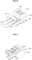
Fig. 1H is a perspective view showing the state of the high-frequency package in a middle step so as to explain the manufacturing method for the high-frequency package according to the first embodiment of the present invention; -
Fig. 1I is a perspective view showing the state of the high-frequency package in a middle step so as to explain the manufacturing method for the high-frequency package according to the first embodiment of the present invention; -
Fig. 1J is a perspective view showing the state of the high-frequency package in a middle step so as to explain the manufacturing method for the high-frequency package according to the first embodiment of the present invention; -
Fig. 1K is a perspective view showing the state of the high-frequency package in a middle step so as to explain the manufacturing method for the high-frequency package according to the first embodiment of the present invention; -
Fig. 1L is a perspective view showing the state of the high-frequency package in a middle step so as to explain the manufacturing method for the high-frequency package according to the first embodiment of the present invention; -
Fig. 1M is a perspective view showing the state of the high-frequency package in a middle step so as to explain the manufacturing method for the high-frequency package according to the first embodiment of the present invention; -
Fig. 1N is a perspective view showing the state of the high-frequency package in a middle step so as to explain the manufacturing method for the high-frequency package according to the first embodiment of the present invention; -
Fig. 1O is a perspective view showing the state of the high-frequency package in a middle step so as to explain the manufacturing method for the high-frequency package according to the first embodiment of the present invention; -
Fig. 1P is a perspective view showing the state of the high-frequency package in a middle step so as to explain the manufacturing method for the high-frequency package according to the first embodiment of the present invention; -
Fig. 2A is a perspective view showing the state of a high-frequency package in a middle step so as to explain a manufacturing method for a high-frequency package according to the second embodiment of the present invention; -
Fig. 2B is a perspective view showing the state of the high-frequency package in a middle step so as to explain the manufacturing method for the high-frequency package according to the second embodiment of the present invention; -
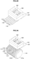
Fig. 2C is a perspective view showing the state of the high-frequency package in a middle step so as to explain the manufacturing method for the high-frequency package according to the second embodiment of the present invention; -
Fig. 2D is a perspective view showing the state of the high-frequency package in a middle step so as to explain the manufacturing method for the high-frequency package according to the second embodiment of the present invention; -
Fig. 3A is a perspective view showing the state of a high-frequency package in a middle step so as to explain a manufacturing method for a high-frequency package according to the third embodiment of the present invention; -
Fig. 3B is a perspective view showing the state of the high-frequency package in a middle step so as to explain the manufacturing method for the high-frequency package according to the third embodiment of the present invention; -
Fig. 3C is a perspective view showing the state of the high-frequency package in a middle step so as to explain the manufacturing method for the high-frequency package according to the third embodiment of the present invention; -
Fig. 4A is a perspective view showing the state of a high-frequency package in a middle step so as to explain a manufacturing method for a high-frequency package according to the fourth embodiment of the present invention; -
Fig. 4B is a perspective view showing the state of the high-frequency package in a middle step so as to explain the manufacturing method for the high-frequency package according to the fourth embodiment of the present invention; -
Fig. 4C is a perspective view showing the state of the high-frequency package in a middle step so as to explain the manufacturing method for the high-frequency package according to the fourth embodiment of the present invention; -
Fig. 4D is a perspective view showing the state of the high-frequency package in a middle step so as to explain the manufacturing method for the high-frequency package according to the fourth embodiment of the present invention; -
Fig. 4E is a perspective view showing the state of the high-frequency package in a middle step so as to explain the manufacturing method for the high-frequency package according to the fourth embodiment of the present invention; -
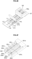
Fig. 4F is a perspective view showing the state of the high-frequency package in a middle step so as to explain the manufacturing method for the high-frequency package according to the fourth embodiment of the present invention; -
Fig. 4G is a perspective view showing the state of the high-frequency package in a middle step so as to explain the manufacturing method for the high-frequency package according to the fourth embodiment of the present invention; -
Fig. 4H is a perspective view showing the state of the high-frequency package in a middle step so as to explain the manufacturing method for the high-frequency package according to the fourth embodiment of the present invention; -
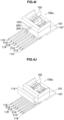
Fig. 4I is a perspective view showing the state of the high-frequency package in a middle step so as to explain the manufacturing method for the high-frequency package according to the fourth embodiment of the present invention; -
Fig. 4J is a perspective view showing the state of the high-frequency package in a middle step so as to explain the manufacturing method for the high-frequency package according to the fourth embodiment of the present invention; -
Fig. 4K is a perspective view showing the state of the high-frequency package in a middle step so as to explain the manufacturing method for the high-frequency package according to the fourth embodiment of the present invention; -
Fig. 5 is an explanatory view showing the configuration of a conventional high-frequency package; -
Fig. 6 is a view showing the configuration of a conventional optical reception module; and -
Fig. 7 is a perspective view showing the configuration of a part of the conventional high-frequency package. - A manufacturing method for a high-frequency package according to an embodiment of the present invention will be described below.
- A manufacturing method for a high-frequency package according to the first embodiment of the present invention will be described first with reference to
Figs. 1A to 1P . - First, as shown in
Figs. 1A and 1B , a packagemain body 100 is prepared (first step). The packagemain body 100 includes asubstrate 101 formed by alternately laminated insulator layers and conductor layers, a first differentialcoplanar line 102 formed on the surface of thesubstrate 101, and a second differentialcoplanar line 103 formed on the back surface on the side of the mounting surface of thesubstrate 101 and connected to the first differentialcoplanar line 102. Note thatFig. 1B shows the side of the mounting surface of the package main body 100 (substrate 101). Also, aspacer 107 configured to make the distance constant between a part of the packagemain body 100 and a mounting board on which these are mounted is provided on the package main body 100 (substrate 101) . - Also, the package
main body 100 includes afirst signal pad 104, asecond signal pad 105, and twoground pads 106. Thefirst signal pad 104 is arranged on the side of the back surface (mounting surface) of thesubstrate 101 and connected to the first signal line of the second differentialcoplanar line 103. Thesecond signal pad 105 is arranged on the side of the back surface of thesubstrate 101 and connected to the second signal line of the second differentialcoplanar line 103. Thefirst signal pad 104 and thesecond signal pad 105 have an interval that gradually increases from the center side of the packagemain body 100 toward an end side. The twoground pads 106 are arranged on the side of the back surface of thesubstrate 101 and connected to the two ground lines of the second differentialcoplanar line 103. - Next, as shown in
Figs. 1C, 1D, and 1E , afirst lead frame 110 is prepared (second step), and asecond lead frame 112 is prepared (third step). - The
first lead frame 110 includes a plate-shapedfirst frame 111, afirst lead 114, and asecond lead 115. Thefirst lead 114 and thesecond lead 115 respectively include linear portions extending on a plane including the plane of thefirst frame 111,bent portions first frame 111, anddistal end portions bent portions distal end portion 114b of thefirst lead 114 and thedistal end portion 115b of thesecond lead 115 is the interval between thefirst signal pad 104 and thesecond signal pad 105. Note that the interval between thefirst signal pad 104 and thesecond signal pad 105 is narrower than the interval between thefirst signal pad 104 and theground pad 106, which are adjacent to each other, and the interval between thesecond signal pad 105 and theground pad 106, which are adjacent to each other. - Additionally, in the first embodiment, the
first lead frame 110 has a shape in which the interval between thefirst lead 114 and thesecond lead 115 becomes wider from the side of thedistal end portions first frame 111. Also, in thefirst lead 114 and thesecond lead 115,thin portions - The
second lead frame 112 includes asecond frame 113 and two third leads 116. Each of the twothird leads 116 includes a linear portion extending on a plane including the plane of thesecond frame 113, abent portion 116a that is bent in a direction for separating from the plane including the plane of thesecond frame 113, and adistal end portion 116b at the tip of thebent portion 116a. Also, the interval between thedistal end portions 116b of the twothird leads 116 is the interval between the twoground pads 106. Note that in the first embodiment, thesecond lead frame 112 has a shape in which the interval between the twothird leads 116 is the same interval from the side of thedistal end portions 116b to the side of thesecond frame 113. Also, in eachthird lead 116, athin portion 116c having a small thickness is provided in the middle of the linear portion to facilitate a cutting work to be performed in post-processing. - The
first lead frame 110 and thesecond lead frame 112 are arranged at a predetermined position and overlaid. At this time, in aregion 117 of the linear portion of a predetermined length from the bent portion, the positions of the bottom surfaces of the leads are made to match. Theregion 117 can be used as a reference plane in post-processing. - Next, as shown in
Figs. 1F and 1G , thedistal end portion 114b of thefirst lead 114 of thefirst lead frame 110 is connected to thefirst signal pad 104, thedistal end portion 115b of thesecond lead 115 is connected to thesecond signal pad 105, and thedistal end portion 116b of thethird lead 116 of thesecond lead frame 112 is connected to the ground pad 106 (fourth step). For example, the above-described connection can be done by soldering using silver solder or the like. Note that in the first embodiment, the interval gradually decreases from the end portion of the packagemain body 100 toward the center side. In the same way as in this state, the interval between thefirst lead 114 and thesecond lead 115 gradually decreases toward thedistal end portions - After the above-described fourth step, the
first frame 111 is separated from thefirst lead 114 and thesecond lead 115, and thesecond frame 113 is separated from the third leads 116 (fifth step). For example, as shown inFig. 1H , the thin portions with a small thickness in the middle of the linear portions of the leads are cut at once using acutting blade 118 to make each lead have a predetermined length. After the cutting, as shown inFig. 1I , the finish shape of thefirst lead 114 and thesecond lead 115 and the finish shape of the third leads 116 are different. The interval between thefirst lead 114 and thesecond lead 115 gradually changes and decreases from the cut end indicated by a dotted ellipse inFig. 1I toward the bent portions. - Next, after the fifth step, the interval between the linear portion of the
first lead 114 and the linear portion of thesecond lead 115 is adjusted (sixth step). First, as shown inFig. 1J , a holdingjig 121 is fixed to the side of the mounting surface of the packagemain body 100. Next, as shown inFigs. 1K ,1L, and 1M , the interval between the linear portion of thefirst lead 114 and the linear portion of thesecond lead 115 is adjusted using a leadshape changing jig 122. - The lead
shape changing jig 122 includes abase portion 122a, and projectingportions base portion 122a. Each of the projectingportions portions base portion 122a). The width of each of the projectingportions portions base portion 122a. - The
first lead 114 and thesecond lead 115 are arranged between the projectingportion 122b and the projectingportion 122c, and the packagemain body 100 with the holdingjig 121 fixed on it is slid in the vertical direction to the side of thebase portion 122a of the leadshape changing jig 122. Accordingly, thefirst lead 114 and thesecond lead 115 are deformed along the gradually decreasing interval between the projectingportion 122b and the projectingportion 122c, and the interval between thefirst lead 114 and thesecond lead 115 gradually changes (decreases). - When all leads reach the upper surface of the
base portion 122a, the interval between the linear portion of thefirst lead 114 and the linear portion of thesecond lead 115 becomes equal over the whole area (the pitches become even). In addition, when all leads reach the upper surface of thebase portion 122a, this state is held, and apressing jig 123 is pressed from above in this state. After that, all jigs are detached. This makes it possible to align the height positions of thefirst lead 114 and thesecond lead 115 in the plane direction of thesubstrate 101, as shown inFig. 1N . - Next, the lengths of the
first lead 114, thesecond lead 115, and the third leads 116 are aligned (seventh step). For example, as shown inFig. 1O , the leads are cut at once using thecutting blade 118, thereby aligning the lengths of thefirst lead 114, thesecond lead 115, and the third leads 116, as shown inFig. 1P . - When completed, a high-frequency package in which the pitches between the third leads 116 serving as ground lead pins and the
first lead 114 and thesecond lead 115 serving as signal lead pins are aligned can be obtained. By the manufacturing method according to the above-described first embodiment, even if the pitches of the differential signal lines in the package main body are narrow, the pitch width of the differential signal lead pins can be made wider than that. This can align the pitches of all lead pins and make contribution to improvement of productivity when mounting the package on a board. - A manufacturing method for a high-frequency package according to the second embodiment of the present invention will be described next with reference to
Figs. 2A to 2D . - First, as is the first embodiment, as described with reference to
Figs. 1A and 1B , a packagemain body 100 is prepared (first step). Next, as described with reference toFigs. 1C, 1D, and 1E , afirst lead frame 110 is prepared (second step), and asecond lead frame 112 is prepared (third step). - Next, as described with reference to
Figs. 1F and 1G , adistal end portion 114b of afirst lead 114 of thefirst lead frame 110 is connected to afirst signal pad 104, adistal end portion 115b of asecond lead 115 is connected to asecond signal pad 105, and adistal end portion 116b of athird lead 116 of thesecond lead frame 112 is connected to a ground pad 106 (fourth step). - After the above-described fourth step, the
first frame 111 is separated from thefirst lead 114 and thesecond lead 115, and thesecond frame 113 is separated from the third leads 116 by the same method as in the above-described first embodiment (fifth step). - Next, after the fifth step, the interval between the linear portion of the
first lead 114 and the linear portion of thesecond lead 115 is adjusted (sixth step). First, as shown inFig. 2A , a leadshape changing jig 131 is prepared. In the second embodiment, the packagemain body 100 is slid in a predetermined direction on the surface of the leadshape changing jig 131, thereby adjusting the interval between the linear portion of thefirst lead 114 and the linear portion of thesecond lead 115. - The lead
shape changing jig 131 includes abase portion 131a, guides 131b provided at the two ends of the upper surface of thebase portion 131a, and a plurality ofprojections 131c aligned on the upper surface of thebase portion 131a. The interval between the twoguides 131b is the same as the width between the outer sides of the twothird leads 116 arranged outside. - Also, each of the plurality of
projections 131c has a rectangular shape in a planar view, which has long sides in the direction (slide direction) for sliding the packagemain body 100. The interval between theprojections 131c adjacent to each other is the same as the width of each lead. In addition, the width of each of the plurality ofprojections 131c in the array direction equals the interval to arrange the bent portions of the leads. - First, as shown in
Fig. 2B , the packagemain body 100 is mounted on the upper surface of thebase portion 131a provided with the plurality ofprojections 131c. At this time, the array direction of the pads provided on the mounting surface of asubstrate 101 is set vertical to the slide direction. In addition, on one end side of the plurality ofprojections 131c, the bent portions of the leads are fitted between theprojections 131c adjacent to each other. - When the package
main body 100 is mounted on the upper surface of thebase portion 131a, as described above, the packagemain body 100 is slid in the slide direction (Fig. 2C ). By this slide, the interval between thefirst lead 114 and thesecond lead 115 gradually changes (decreases). When the cut ends of the leads are moved up to the center of the plurality ofprojections 131c, and the leadshape changing jig 131 is detached after that, the interval between the linear portion of thefirst lead 114 and the linear portion of thesecond lead 115 becomes equal over the whole area (the pitches become even), as shown inFig. 2D . - After that, the lengths of the
first lead 114, thesecond lead 115, and the third leads 116 are aligned, as in the above-described first embodiment (seventh step). When completed, a high-frequency package in which the pitches between the third leads 116 serving as ground lead pins and thefirst lead 114 and thesecond lead 115 serving as signal lead pins are aligned can be obtained. As the characteristic feature of the second embodiment, the pitches of the differential signal lead pins are corrected using a slide-type lead shape changing jig. - By the manufacturing method according to the above-described second embodiment, even if the pitches of the differential signal lines in the package main body are narrow, the pitch width of the differential signal lead pins can be made wider than that. This can align the pitches of all lead pins and make contribution to improvement of productivity when mounting the package on a board.
- A manufacturing method for a high-frequency package according to the third embodiment of the present invention will be described next with reference to
Figs. 3A to 3C . - First, as is the first embodiment, as described with reference to
Figs. 1A and 1B , a packagemain body 100 is prepared (first step). Next, as described with reference toFigs. 1C, 1D, and 1E , afirst lead frame 110 is prepared (second step), and asecond lead frame 112 is prepared (third step). - Next, as described with reference to
Figs. 1F and 1G , adistal end portion 114b of afirst lead 114 of thefirst lead frame 110 is connected to afirst signal pad 104, adistal end portion 115b of asecond lead 115 is connected to asecond signal pad 105, and adistal end portion 116b of athird lead 116 of thesecond lead frame 112 is connected to a ground pad 106 (fourth step). - After the above-described fourth step, the
first frame 111 is separated from thefirst lead 114 and thesecond lead 115, and thesecond frame 113 is separated from the third leads 116 by the same method as in the above-described first embodiment (fifth step). - Next, after the fifth step, the interval between the linear portion of the
first lead 114 and the linear portion of thesecond lead 115 is adjusted (sixth step). First, as shown inFig. 3A , a rotation-type leadshape changing jig 141 is prepared. In the third embodiment, for the packagemain body 100, the leadshape changing jig 141 having a columnar shape is rotated about its axis, thereby sliding the packagemain body 100 relatively in the rotation direction on the outer peripheral surface of the leadshape changing jig 141 and adjusting the interval between the linear portion of thefirst lead 114 and the linear portion of thesecond lead 115. - The lead
shape changing jig 141 includes amain body 141a having a columnar shape, and a plurality ofgrooves 141b formed in the outer peripheral surface of themain body 141a. The plurality ofgrooves 141b extend in the circumferential direction, and the groove width is the same as the width of each lead. In addition, the interval between theadjacent grooves 141b equals the interval to arrange the bent portions of the leads. - First, as shown in
Fig. 3A , the packagemain body 100 is mounted on the peripheral surface of the leadshape changing jig 141, in which the plurality ofgrooves 141b are formed. At this time, the array direction of the pads provided on the mounting surface of asubstrate 101 is set vertical to the circumferential direction (slide direction) of the peripheral surface. In addition, the bent portion of each lead is fitted in a corresponding one of thegrooves 141b. - When the package
main body 100 is mounted, on the upper surface of thebase portion 131a, on the peripheral surface of the leadshape changing jig 141, as described above, the lead shape changing jig 141 (main body 141a) is rotated about the axis. By this rotation, the portions of the leads, which are fitted in thegrooves 141b, are moved from the bent portions of the leads in the direction of the cut ends. When the fitted portions move along with the rotation, the interval between thefirst lead 114 and thesecond lead 115 gradually changes (decreases). As shown inFig. 3B , when the cut end of each lead is fitted in a corresponding one of thegrooves 141b, and the leadshape changing jig 141 is detached after that, the interval between the linear portion of thefirst lead 114 and the linear portion of thesecond lead 115 becomes equal over the whole area (the pitches become even), as shown inFig. 3C . - After that, the lengths of the
first lead 114, thesecond lead 115, and the third leads 116 are aligned, as in the above-described first embodiment (seventh step). When completed, a high-frequency package in which the pitches between the third leads 116 serving as ground lead pins and thefirst lead 114 and thesecond lead 115 serving as signal lead pins are aligned can be obtained. As the characteristic feature of the third embodiment, the pitches of the differential signal lead pins are corrected using a slide-type lead shape changing jig. - By the manufacturing method according to the above-described third embodiment, even if the pitches of the differential signal lines in the package main body are narrow, the pitch width of the differential signal lead pins can be made wider than that. This can align the pitches of all lead pins and make contribution to improvement of productivity when mounting the package on a board.
- A manufacturing method for a high-frequency package according to the fourth embodiment of the present invention will be described next with reference to
Figs. 4A to 4K . - First, as shown in
Fig. 4A , a packagemain body 100a is prepared (first step). The packagemain body 100a includes asubstrate 101 made of an insulator, a first differentialcoplanar line 102 formed on the surface of thesubstrate 101, and a second differentialcoplanar line 103 formed on the back surface on the side of the mounting surface of thesubstrate 101 and connected to the first differentialcoplanar line 102. Note thatFig. 1B shows the side of the mounting surface of the packagemain body 100a (substrate 101). Also, aspacer 107 configured to make the distance constant between a part of the packagemain body 100 and a mounting board on which these are mounted is provided on the packagemain body 100a (substrate 101). - Also, the package
main body 100a includes afirst signal pad 204, asecond signal pad 205, and twoground pads 106. Thefirst signal pad 204 is arranged on the side of the back surface (mounting surface) of thesubstrate 101 and connected to the first signal line of the second differentialcoplanar line 103. Thesecond signal pad 205 is arranged on the side of the back surface of thesubstrate 101 and connected to the second signal line of the second differentialcoplanar line 103. Thefirst signal pad 204 and thesecond signal pad 205 have the same interval from the center side of the packagemain body 100a toward an end side. The twoground pads 106 are arranged on the side of the back surface of thesubstrate 101 and connected to the two ground lines of the second differentialcoplanar line 103. - Next, as shown in
Figs. 4B and4C , afirst lead frame 210 is prepared (second step), and asecond lead frame 112 is prepared (third step). Thesecond lead frame 112 is the same as in the above-described first embodiment, and a detailed description thereof will be omitted. - The
first lead frame 210 includes a plate-shapedfirst frame 211, afirst lead 214, and asecond lead 215. Thefirst lead 214 and thesecond lead 215 respectively include linear portions extending on a plane including the plane of thefirst frame 211,bent portions first frame 211, anddistal end portions bent portions distal end portion 214b of thefirst lead 214 and thedistal end portion 215b of thesecond lead 215 is the interval between thefirst signal pad 204 and thesecond signal pad 205. Note that the interval between thefirst signal pad 204 and thesecond signal pad 205 is narrower than the interval between thefirst signal pad 204 and theground pad 106, which are adjacent to each other, and the interval between thesecond signal pad 205 and theground pad 106, which are adjacent to each other. - Additionally, in the fourth embodiment, the
first lead frame 210 has a shape in which the interval between thefirst lead 214 and thesecond lead 215 is the same interval from the side of thedistal end portions first frame 211. Also, in thefirst lead 214 and thesecond lead 215,thin portions - The
first lead frame 210 and thesecond lead frame 112 are arranged at a predetermined position and overlaid. Note that in the fourth embodiment as well, in a region of the linear portion of a predetermined length from the bent portion, the positions of the bottom surfaces of the leads are made to match. This region can be used as a reference plane in post-processing. - Next, the
distal end portion 214b of thefirst lead 214 of thefirst lead frame 210 is connected to thefirst signal pad 204, thedistal end portion 215b of thesecond lead 215 is connected to thesecond signal pad 205, and thedistal end portion 116b of thethird lead 116 of thesecond lead frame 112 is connected to the ground pad 106 (fourth step). For example, the above-described connection can be done by soldering using silver solder or the like.Fig. 4D shows a state in which the lead frames are connected. - After the above-described fourth step, the
first frame 211 is separated from thefirst lead 214 and thesecond lead 215, and thesecond frame 113 is separated from the third leads 116 (fifth step). For example, as shown inFig. 4E , the thin portions with a small thickness in the middle of the linear portions of the leads are cut at once using acutting blade 118 to make each lead have a predetermined length. After the cutting, in the fourth embodiment, the finish shape of thefirst lead 214 and thesecond lead 215 and the finish shape of the third leads 116 are the same. - Next, after the fifth step, the interval between the linear portion of the
first lead 214 and the linear portion of thesecond lead 215 is adjusted (sixth step). In this adjustment, abase jig 201 and acorrection jig 202 shown inFig. 4F are used. Thebase jig 201 includes aguide groove 201a configured to slide thecorrection jig 202, and afirst guiderail 201b and asecond guiderail 201c, which are formed across the region where theguide groove 201a is formed. In addition, thesecond guiderail 201c is provided with agroove 201d in which thethird lead 116 is fitted. - On the other hand, the
correction jig 202 includes aslide projection 202a fitted in theguide groove 201a, and aconvex portion 202b configured to increase the interval between thefirst lead 214 and thesecond lead 215. The width of theconvex portion 202b decreases toward the side of adistal end 202c. - First, as shown in
Fig. 4G , thebase jig 201 is arranged on the side of the mounting surface of the packagemain body 100a, and thefirst lead 214 and thesecond lead 215 are arranged between thefirst guiderail 201b and thesecond guiderail 201c. In addition, thefirst lead 214 and thethird lead 116 on the outer side are arranged across thefirst guiderail 201b. Thethird lead 116 at the center is fitted in thegroove 201d. - Next, the
slide projection 202a of thecorrection jig 202 is fitted in theguide groove 201a. Also, between thefirst guiderail 201b and thesecond guiderail 201c, thedistal end 202c of theconvex portion 202b is inserted between thefirst lead 214 and thesecond lead 215. In this state, the state in which theslide projection 202a is fitted in theguide groove 201a is maintained, and thecorrection jig 202 is slid from the cut end side of the leads to the side of the bent portions (Fig. 4H ). - By the slide of the above-described
correction jig 202, theconvex portion 202b inserted between thefirst lead 214 and thesecond lead 215 increases (adjusts) the interval between thefirst lead 214 and thesecond lead 215. When the slidcorrection jig 202 reaches the packagemain body 100a, the interval between the linear portion of thefirst lead 214 and the linear portion of thesecond lead 215 is increased over the whole area, and the intervals between the leads become equal (the pitches become even). - In the fourth embodiment, when the intervals between the leads are made equal by the above-described processing, the interval between the linear portions of the
first lead 214 and thesecond lead 215 becomes wider than the interval between thefirst signal pad 204 and the second signal pad 205 (Fig. 41 ). - Next, the lengths of the
first lead 214, thesecond lead 215, and the third leads 116 are aligned (seventh step). For example, as shown inFig. 4J , the leads are cut at once using thecutting blade 118, thereby aligning the lengths of thefirst lead 214, thesecond lead 215, and the third leads 116, as shown inFig. 4K . - When completed, a high-frequency package in which the pitches between the third leads 116 serving as ground lead pins and the
first lead 214 and thesecond lead 215 serving as signal lead pins are aligned can be obtained. By the manufacturing method according to the above-described fourth embodiment, even if the pitches of the differential signal lines in the package main body are narrow, the pitch width of the differential signal lead pins can be made wider than that. This can align the pitches of all lead pins and make contribution to improvement of productivity when mounting the package on a board. - As described above, according to the present invention, after the distal end portion of the first lead of the first lead frame is connected to the first signal pad, and the distal end portion of the second lead is connected to the second signal pad, the interval between the linear portion of the first lead and the linear portion of the second lead is adjusted. It is therefore possible to provide an efficient manufacturing method for a high-frequency package, which changes the interval between lead pins.
- Note that the present invention is not limited to the above-described embodiments, and it is obvious that many modifications and combinations can be made by a person skilled in the art in this field within the technical scope of the present invention.
- 100...package main body, 101... substrate, 102...first differential coplanar line, 103...second differential coplanar line, 104...first signal pad, 105...second signal pad, 106...ground pad, 107...spacer, 110...first lead frame, 111...first frame, 113...second frame, 114...first lead, 114a...bent portion, 114b...distal end portion, 114c...thin portion, 115...second lead, 115a...bent portion, 115b...distal end portion, 115c...thin portion, 116...third lead, 116a...bent portion, 116b...distal end portion, 116c...thin portion, 117...region, 118...cutting blade, 121... holding jig, 122...lead shape changing jig, 122a...base portion, 122b...projecting portion, 122c...projecting portion, 123...pressing jig.
Claims (6)
- A manufacturing method for a high-frequency package, comprising:
a first step of preparing a package main body including:a substrate formed of alternately laminated insulator layers and conductor layers,a first differential coplanar line formed on a surface of the substrate,a second differential coplanar line formed on a back surface of the substrate on a side of a mounting surface of the substrate and connected to the first differential coplanar line,a first signal pad arranged on a side of the back surface of the substrate and connected to a first signal line of the second differential coplanar line,a second signal pad arranged on the side of the back surface of the substrate and connected to a second signal line of the second differential coplanar line, andtwo ground pads arranged on the side of the back surface of the substrate and connected to two ground lines of the second differential coplanar line;a second step of preparing a first lead frame including a plate-shaped first frame, a first lead, and a second lead, each of the first lead and the second lead including a linear portion extending on a plane including a plane of the first frame, a bent portion bent in a direction for separating from the plane including the plane of the first frame, and a distal end portion at a tip of the bent portion, in which an interval between the distal end portion of the first lead and the distal end portion of the second lead is an interval between the first signal pad and the second signal pad;a third step of preparing a second lead frame including a second frame and two third leads, each of the two third leads including a linear portion extending on a plane including a plane of the second frame, a bent portion bent in a direction for separating from the plane including the plane of the second frame, and a distal end portion at a tip of the bent portion, in which an interval between the distal end portions of the two third leads is an interval between the two ground pads;a fourth step of connecting the distal end portion of the first lead of the first lead frame to the first signal pad, connecting the distal end portion of the second lead to the second signal pad, and connecting the distal end portion of the third lead of the second lead frame to the ground pad;a fifth step of, after the fourth step, separating the first frame from the first lead and the second lead, and separating the second frame from the third leads;a sixth step of, after the fifth step, adjusting an interval between the linear portion of the first lead and the linear portion of the second lead; anda seventh step of, after the sixth step, aligning lengths of the first lead, the second lead, and the third leads. - The manufacturing method for the high-frequency package according to claim 1, whereinthe first lead frame has a shape in which the interval between the first lead and the second lead becomes wider from a side of the distal end portions to a side of the first frame, andthe second lead frame has a shape in which the interval between the two third leads is the same interval from a side of the distal end portions to a side of the second frame.
- The manufacturing method for the high-frequency package according to claim 2, wherein
in the sixth step, the interval between the linear portion of the first lead and the linear portion of the second lead is decreased to equalize the intervals between the linear portion of the first lead, the linear portion of the second lead, and the linear portion of the third lead. - The manufacturing method for the high-frequency package according to claim 1, whereinthe first lead frame has a shape in which the interval between the first lead and the second lead is the same interval from a side of the distal end portions to a side of the first frame, andthe second lead frame has a shape in which the interval between the two third leads is the same interval from a side of the distal end portions to a side of the second frame.
- The manufacturing method for the high-frequency package according to claim 4, wherein
in the sixth step, the interval between the linear portion of the first lead and the linear portion of the second lead is increased to equalize the intervals between the linear portion of the first lead, the linear portion of the second lead, and the linear portion of the third lead. - The manufacturing method for the high-frequency package according to any one of claims 1 to 5, wherein
the interval between the first signal pad and the second signal pad is narrower than an interval between the first signal pad and the ground pad, which are adjacent to each other, and an interval between the second signal pad and the ground pad, which are adjacent to each other.
Applications Claiming Priority (1)
| Application Number | Priority Date | Filing Date | Title |
|---|---|---|---|
| PCT/JP2020/029206 WO2022024289A1 (en) | 2020-07-30 | 2020-07-30 | Production method for high-frequency package |
Publications (3)
| Publication Number | Publication Date |
|---|---|
| EP4191659A1 true EP4191659A1 (en) | 2023-06-07 |
| EP4191659A4 EP4191659A4 (en) | 2024-05-15 |
| EP4191659B1 EP4191659B1 (en) | 2025-11-05 |
Family
ID=80037836
Family Applications (1)
| Application Number | Title | Priority Date | Filing Date |
|---|---|---|---|
| EP20947171.3A Active EP4191659B1 (en) | 2020-07-30 | 2020-07-30 | Production method for high-frequency package |
Country Status (5)
| Country | Link |
|---|---|
| US (1) | US12272567B2 (en) |
| EP (1) | EP4191659B1 (en) |
| JP (1) | JP7124987B2 (en) |
| CN (1) | CN114450775B (en) |
| WO (1) | WO2022024289A1 (en) |
Families Citing this family (1)
| Publication number | Priority date | Publication date | Assignee | Title |
|---|---|---|---|---|
| JP7803192B2 (en) * | 2022-03-30 | 2026-01-21 | 住友大阪セメント株式会社 | Optical device and optical transmitter using the same |
Family Cites Families (35)
| Publication number | Priority date | Publication date | Assignee | Title |
|---|---|---|---|---|
| ES362566A1 (en) | 1968-07-25 | 1971-02-01 | Sandoz Ag | PROCEDURE FOR OBTAINING AZOIC COMPOUNDS. |
| US4680613A (en) * | 1983-12-01 | 1987-07-14 | Fairchild Semiconductor Corporation | Low impedance package for integrated circuit die |
| JPH0425036A (en) * | 1990-05-16 | 1992-01-28 | Mitsubishi Electric Corp | Microwave semiconductor device |
| JPH04354358A (en) * | 1991-05-31 | 1992-12-08 | Shinko Electric Ind Co Ltd | Multilayer lead frame and its manufacture |
| US5484959A (en) * | 1992-12-11 | 1996-01-16 | Staktek Corporation | High density lead-on-package fabrication method and apparatus |
| EP0867939A3 (en) * | 1997-03-26 | 1999-08-18 | Matsushita Electronics Corporation | Wiring substrate for semiconductor device with externally wired leads |
| US6061251A (en) * | 1997-09-08 | 2000-05-09 | Hewlett-Packard Company | Lead-frame based vertical interconnect package |
| WO2002009180A1 (en) * | 2000-07-25 | 2002-01-31 | Ssi Inc | Plastic package base, air cavity type package and their manufacturing methods |
| JP3823743B2 (en) * | 2001-03-09 | 2006-09-20 | 住友電気工業株式会社 | Optical transmission module with high-frequency signal input terminal |
| JP2003204027A (en) * | 2002-01-09 | 2003-07-18 | Matsushita Electric Ind Co Ltd | Lead frame and method of manufacturing the same, resin-sealed semiconductor device and method of manufacturing the same |
| JP2004095572A (en) * | 2002-08-29 | 2004-03-25 | Hitachi Ltd | Semiconductor device and method of manufacturing the same |
| TWI229422B (en) * | 2003-12-05 | 2005-03-11 | Via Tech Inc | A bonding-wire structure having desirable high-frequency characteristics for using in metal frame package |
| KR20060021744A (en) * | 2004-09-04 | 2006-03-08 | 삼성테크윈 주식회사 | Lead frame and manufacturing method |
| EP1746648A3 (en) * | 2005-07-22 | 2008-09-03 | Marvell World Trade Ltd. | Packaging for high speed integrated circuits |
| JP4970924B2 (en) * | 2006-03-28 | 2012-07-11 | 三菱電機株式会社 | Optical element package and optical semiconductor device using the same |
| US8124461B2 (en) * | 2006-12-27 | 2012-02-28 | Mediatek Inc. | Method for manufacturing leadframe, packaging method for using the leadframe and semiconductor package product |
| JP2009212400A (en) * | 2008-03-05 | 2009-09-17 | Ngk Spark Plug Co Ltd | High-frequency package |
| JP4921498B2 (en) * | 2009-01-28 | 2012-04-25 | 日本電信電話株式会社 | Semiconductor package and mounting method thereof |
| JP2011134789A (en) * | 2009-12-22 | 2011-07-07 | Mitsubishi Electric Corp | Semiconductor device, and printed circuit board |
| JP5242605B2 (en) * | 2010-01-28 | 2013-07-24 | ルネサスエレクトロニクス株式会社 | Wiring structure |
| JP2011155184A (en) * | 2010-01-28 | 2011-08-11 | Renesas Electronics Corp | Interconnection structure |
| JP4934733B2 (en) | 2010-03-16 | 2012-05-16 | 日本電信電話株式会社 | Optical receiver module |
| US8592960B2 (en) * | 2010-08-31 | 2013-11-26 | Viasat, Inc. | Leadframe package with integrated partial waveguide interface |
| TWI453831B (en) * | 2010-09-09 | 2014-09-21 | 台灣捷康綜合有限公司 | Semiconductor package and method for making the same |
| US8937374B2 (en) * | 2011-12-22 | 2015-01-20 | Panasonic Corporation | Semiconductor package, method and mold for producing same, input and output terminals of semiconductor package |
| TWI449475B (en) * | 2012-01-09 | 2014-08-11 | Novatek Microelectronics Corp | Printed circuit board |
| US9269653B2 (en) * | 2012-06-27 | 2016-02-23 | Mediatek Inc. | SGS or GSGSG pattern for signal transmitting channel, and PCB assembly, chip package using such SGS or GSGSG pattern |
| JP6162800B2 (en) * | 2013-05-29 | 2017-07-12 | 京セラ株式会社 | Device storage package and mounting structure |
| US9171788B1 (en) * | 2014-09-30 | 2015-10-27 | Alpha And Omega Semiconductor Incorporated | Semiconductor package with small gate clip and assembly method |
| CN104795379B (en) * | 2015-04-30 | 2017-06-27 | 南通大学 | Differential coplanar transmission line package pin internal and external cascade structure |
| US9972587B2 (en) * | 2016-03-02 | 2018-05-15 | Panasonic Intellectual Property Management Co., Ltd. | Signal transmission device using electromagnetic resonance coupler |
| TWM540453U (en) * | 2016-11-16 | 2017-04-21 | Luxnet Corp | Soldering structure of flexible and hard printed circuit boards |
| CN107369667A (en) * | 2016-05-13 | 2017-11-21 | 松下电器产业株式会社 | Device for signalling |
| CN109417054B (en) * | 2016-06-27 | 2022-11-15 | Ngk电子器件株式会社 | Ceramic substrate for high frequency and semiconductor element housing package for high frequency |
| JP7139965B2 (en) * | 2019-01-16 | 2022-09-21 | 日本電信電話株式会社 | Semiconductor Mach-Zehnder optical modulator |
-
2020
- 2020-07-30 EP EP20947171.3A patent/EP4191659B1/en active Active
- 2020-07-30 WO PCT/JP2020/029206 patent/WO2022024289A1/en not_active Ceased
- 2020-07-30 CN CN202080068403.3A patent/CN114450775B/en active Active
- 2020-07-30 JP JP2022502116A patent/JP7124987B2/en active Active
- 2020-07-30 US US17/765,475 patent/US12272567B2/en active Active
Also Published As
| Publication number | Publication date |
|---|---|
| US12272567B2 (en) | 2025-04-08 |
| JPWO2022024289A1 (en) | 2022-02-03 |
| CN114450775A (en) | 2022-05-06 |
| WO2022024289A1 (en) | 2022-02-03 |
| EP4191659B1 (en) | 2025-11-05 |
| CN114450775B (en) | 2025-09-09 |
| JP7124987B2 (en) | 2022-08-24 |
| EP4191659A4 (en) | 2024-05-15 |
| US20220375766A1 (en) | 2022-11-24 |
Similar Documents
| Publication | Publication Date | Title |
|---|---|---|
| US11605869B2 (en) | Electronic apparatus and electrical element | |
| US20030092291A1 (en) | High speed electrical connector | |
| US7527501B2 (en) | Coaxial connector, connector assembly, printed circuit board and electronic apparatus | |
| US20100068933A1 (en) | High-speed transmission connector, plug for high-speed transmission connector, and socket for high-speed transmission connector | |
| US9173292B1 (en) | Edge launch transition for a printed circuit board | |
| JP2002368372A (en) | Circuit board, battery pack including the same, and method of manufacturing circuit board | |
| EP4191659B1 (en) | Production method for high-frequency package | |
| JP2009004460A (en) | Optical communication module and forming method of wiring pattern | |
| US12512613B2 (en) | High-frequency signal transmission device and electrical connection method for wiring board and connector | |
| US12426155B2 (en) | Flexible printed circuit board comprising power transmission line | |
| JP2001102712A (en) | Wiring board with connector and manufacturing method therefor | |
| JP3680792B2 (en) | Multi-connector for high-speed communication apparatus and mounting method of multi-connector for high-speed communication apparatus and printed circuit board | |
| US20240280607A1 (en) | Electrical test contact terminal for a pin-type device lead | |
| JP2013065657A (en) | Printed wiring board, and method for wiring printed wiring board | |
| US20220344289A1 (en) | High Frequency Package | |
| CN115561494B (en) | Probe card | |
| CN218005296U (en) | Connector with a locking member | |
| US20190230786A1 (en) | Flexible circuit board with improved bonding position accuracy | |
| JP7255705B2 (en) | High frequency line structure, subassembly, line card, and method of manufacturing high frequency line structure | |
| JP2005044966A (en) | Optical semiconductor module and optical semiconductor device | |
| JP2004047532A (en) | Module device for optical communication | |
| TW202541368A (en) | Compact high speed near chip connector | |
| JP5510190B2 (en) | Flat cable connection structure | |
| CN115561494A (en) | Probe card | |
| JP2007158880A (en) | antenna |
Legal Events
| Date | Code | Title | Description |
|---|---|---|---|
| STAA | Information on the status of an ep patent application or granted ep patent |
Free format text: STATUS: THE INTERNATIONAL PUBLICATION HAS BEEN MADE |
|
| PUAI | Public reference made under article 153(3) epc to a published international application that has entered the european phase |
Free format text: ORIGINAL CODE: 0009012 |
|
| STAA | Information on the status of an ep patent application or granted ep patent |
Free format text: STATUS: REQUEST FOR EXAMINATION WAS MADE |
|
| 17P | Request for examination filed |
Effective date: 20220325 |
|
| AK | Designated contracting states |
Kind code of ref document: A1 Designated state(s): AL AT BE BG CH CY CZ DE DK EE ES FI FR GB GR HR HU IE IS IT LI LT LU LV MC MK MT NL NO PL PT RO RS SE SI SK SM TR |
|
| DAV | Request for validation of the european patent (deleted) | ||
| DAX | Request for extension of the european patent (deleted) | ||
| A4 | Supplementary search report drawn up and despatched |
Effective date: 20240411 |
|
| RIC1 | Information provided on ipc code assigned before grant |
Ipc: H01L 23/498 20060101ALI20240405BHEP Ipc: H01L 23/495 20060101ALI20240405BHEP Ipc: H01L 21/48 20060101ALI20240405BHEP Ipc: H01L 23/12 20060101AFI20240405BHEP |
|
| GRAP | Despatch of communication of intention to grant a patent |
Free format text: ORIGINAL CODE: EPIDOSNIGR1 |
|
| STAA | Information on the status of an ep patent application or granted ep patent |
Free format text: STATUS: GRANT OF PATENT IS INTENDED |
|
| INTG | Intention to grant announced |
Effective date: 20250527 |
|
| GRAS | Grant fee paid |
Free format text: ORIGINAL CODE: EPIDOSNIGR3 |
|
| RAP3 | Party data changed (applicant data changed or rights of an application transferred) |
Owner name: NTT, INC. |
|
| GRAA | (expected) grant |
Free format text: ORIGINAL CODE: 0009210 |
|
| STAA | Information on the status of an ep patent application or granted ep patent |
Free format text: STATUS: THE PATENT HAS BEEN GRANTED |
|
| AK | Designated contracting states |
Kind code of ref document: B1 Designated state(s): AL AT BE BG CH CY CZ DE DK EE ES FI FR GB GR HR HU IE IS IT LI LT LU LV MC MK MT NL NO PL PT RO RS SE SI SK SM TR |
|
| REG | Reference to a national code |
Ref country code: CH Ref legal event code: F10 Free format text: ST27 STATUS EVENT CODE: U-0-0-F10-F00 (AS PROVIDED BY THE NATIONAL OFFICE) Effective date: 20251105 Ref country code: GB Ref legal event code: FG4D |
|
| REG | Reference to a national code |
Ref country code: DE Ref legal event code: R096 Ref document number: 602020061939 Country of ref document: DE |
|
| REG | Reference to a national code |
Ref country code: DE Ref legal event code: R079 Ref document number: 602020061939 Country of ref document: DE Free format text: PREVIOUS MAIN CLASS: H01L0023120000 Ipc: H10W0070600000 |
|
| REG | Reference to a national code |
Ref country code: IE Ref legal event code: FG4D |
|
| REG | Reference to a national code |
Ref country code: NL Ref legal event code: MP Effective date: 20251105 |
|
| PG25 | Lapsed in a contracting state [announced via postgrant information from national office to epo] |
Ref country code: ES Free format text: LAPSE BECAUSE OF FAILURE TO SUBMIT A TRANSLATION OF THE DESCRIPTION OR TO PAY THE FEE WITHIN THE PRESCRIBED TIME-LIMIT Effective date: 20251105 |
|
| REG | Reference to a national code |
Ref country code: LT Ref legal event code: MG9D |
|
| PG25 | Lapsed in a contracting state [announced via postgrant information from national office to epo] |
Ref country code: NO Free format text: LAPSE BECAUSE OF FAILURE TO SUBMIT A TRANSLATION OF THE DESCRIPTION OR TO PAY THE FEE WITHIN THE PRESCRIBED TIME-LIMIT Effective date: 20260205 |
|
| PG25 | Lapsed in a contracting state [announced via postgrant information from national office to epo] |
Ref country code: FI Free format text: LAPSE BECAUSE OF FAILURE TO SUBMIT A TRANSLATION OF THE DESCRIPTION OR TO PAY THE FEE WITHIN THE PRESCRIBED TIME-LIMIT Effective date: 20251105 Ref country code: HR Free format text: LAPSE BECAUSE OF FAILURE TO SUBMIT A TRANSLATION OF THE DESCRIPTION OR TO PAY THE FEE WITHIN THE PRESCRIBED TIME-LIMIT Effective date: 20251105 Ref country code: AT Free format text: LAPSE BECAUSE OF FAILURE TO SUBMIT A TRANSLATION OF THE DESCRIPTION OR TO PAY THE FEE WITHIN THE PRESCRIBED TIME-LIMIT Effective date: 20251105 |
|
| REG | Reference to a national code |
Ref country code: AT Ref legal event code: MK05 Ref document number: 1855361 Country of ref document: AT Kind code of ref document: T Effective date: 20251105 |
|
| PG25 | Lapsed in a contracting state [announced via postgrant information from national office to epo] |
Ref country code: NL Free format text: LAPSE BECAUSE OF FAILURE TO SUBMIT A TRANSLATION OF THE DESCRIPTION OR TO PAY THE FEE WITHIN THE PRESCRIBED TIME-LIMIT Effective date: 20251105 |
|
| PG25 | Lapsed in a contracting state [announced via postgrant information from national office to epo] |
Ref country code: RS Free format text: LAPSE BECAUSE OF FAILURE TO SUBMIT A TRANSLATION OF THE DESCRIPTION OR TO PAY THE FEE WITHIN THE PRESCRIBED TIME-LIMIT Effective date: 20260205 |
|
| PG25 | Lapsed in a contracting state [announced via postgrant information from national office to epo] |
Ref country code: IS Free format text: LAPSE BECAUSE OF FAILURE TO SUBMIT A TRANSLATION OF THE DESCRIPTION OR TO PAY THE FEE WITHIN THE PRESCRIBED TIME-LIMIT Effective date: 20260305 |
|
| PG25 | Lapsed in a contracting state [announced via postgrant information from national office to epo] |
Ref country code: PT Free format text: LAPSE BECAUSE OF FAILURE TO SUBMIT A TRANSLATION OF THE DESCRIPTION OR TO PAY THE FEE WITHIN THE PRESCRIBED TIME-LIMIT Effective date: 20260305 |
|
| PG25 | Lapsed in a contracting state [announced via postgrant information from national office to epo] |
Ref country code: PL Free format text: LAPSE BECAUSE OF FAILURE TO SUBMIT A TRANSLATION OF THE DESCRIPTION OR TO PAY THE FEE WITHIN THE PRESCRIBED TIME-LIMIT Effective date: 20251105 |
|
| PG25 | Lapsed in a contracting state [announced via postgrant information from national office to epo] |
Ref country code: LV Free format text: LAPSE BECAUSE OF FAILURE TO SUBMIT A TRANSLATION OF THE DESCRIPTION OR TO PAY THE FEE WITHIN THE PRESCRIBED TIME-LIMIT Effective date: 20251105 |
|
| PG25 | Lapsed in a contracting state [announced via postgrant information from national office to epo] |
Ref country code: BG Free format text: LAPSE BECAUSE OF FAILURE TO SUBMIT A TRANSLATION OF THE DESCRIPTION OR TO PAY THE FEE WITHIN THE PRESCRIBED TIME-LIMIT Effective date: 20251105 |