EP4191657A1 - Package and production method therefor - Google Patents
Package and production method therefor Download PDFInfo
- Publication number
- EP4191657A1 EP4191657A1 EP20948557.2A EP20948557A EP4191657A1 EP 4191657 A1 EP4191657 A1 EP 4191657A1 EP 20948557 A EP20948557 A EP 20948557A EP 4191657 A1 EP4191657 A1 EP 4191657A1
- Authority
- EP
- European Patent Office
- Prior art keywords
- frame
- joint
- package
- short side
- long side
- Prior art date
- Legal status (The legal status is an assumption and is not a legal conclusion. Google has not performed a legal analysis and makes no representation as to the accuracy of the status listed.)
- Granted
Links
Images




Classifications
-
- G—PHYSICS
- G02—OPTICS
- G02B—OPTICAL ELEMENTS, SYSTEMS OR APPARATUS
- G02B6/00—Light guides; Structural details of arrangements comprising light guides and other optical elements, e.g. couplings
- G02B6/24—Coupling light guides
- G02B6/42—Coupling light guides with opto-electronic elements
- G02B6/4201—Packages, e.g. shape, construction, internal or external details
- G02B6/4274—Electrical aspects
- G02B6/4279—Radio frequency signal propagation aspects of the electrical connection, high frequency adaptations
-
- H—ELECTRICITY
- H10—SEMICONDUCTOR DEVICES; ELECTRIC SOLID-STATE DEVICES NOT OTHERWISE PROVIDED FOR
- H10W—GENERIC PACKAGES, INTERCONNECTIONS, CONNECTORS OR OTHER CONSTRUCTIONAL DETAILS OF DEVICES COVERED BY CLASS H10
- H10W70/00—Package substrates; Interposers; Redistribution layers [RDL]
- H10W70/60—Insulating or insulated package substrates; Interposers; Redistribution layers
- H10W70/67—Insulating or insulated package substrates; Interposers; Redistribution layers characterised by their insulating layers or insulating parts
- H10W70/68—Shapes or dispositions thereof
- H10W70/6875—Shapes or dispositions thereof being on a metallic substrate, e.g. insulated metal substrates [IMS]
-
- H—ELECTRICITY
- H10—SEMICONDUCTOR DEVICES; ELECTRIC SOLID-STATE DEVICES NOT OTHERWISE PROVIDED FOR
- H10F—INORGANIC SEMICONDUCTOR DEVICES SENSITIVE TO INFRARED RADIATION, LIGHT, ELECTROMAGNETIC RADIATION OF SHORTER WAVELENGTH OR CORPUSCULAR RADIATION
- H10F77/00—Constructional details of devices covered by this subclass
-
- H—ELECTRICITY
- H10—SEMICONDUCTOR DEVICES; ELECTRIC SOLID-STATE DEVICES NOT OTHERWISE PROVIDED FOR
- H10F—INORGANIC SEMICONDUCTOR DEVICES SENSITIVE TO INFRARED RADIATION, LIGHT, ELECTROMAGNETIC RADIATION OF SHORTER WAVELENGTH OR CORPUSCULAR RADIATION
- H10F77/00—Constructional details of devices covered by this subclass
- H10F77/50—Encapsulations or containers
-
- H—ELECTRICITY
- H10—SEMICONDUCTOR DEVICES; ELECTRIC SOLID-STATE DEVICES NOT OTHERWISE PROVIDED FOR
- H10W—GENERIC PACKAGES, INTERCONNECTIONS, CONNECTORS OR OTHER CONSTRUCTIONAL DETAILS OF DEVICES COVERED BY CLASS H10
- H10W20/00—Interconnections in chips, wafers or substrates
- H10W20/40—Interconnections external to wafers or substrates, e.g. back-end-of-line [BEOL] metallisations or vias connecting to gate electrodes
- H10W20/41—Interconnections external to wafers or substrates, e.g. back-end-of-line [BEOL] metallisations or vias connecting to gate electrodes characterised by their conductive parts
- H10W20/43—Layouts of interconnections
-
- H—ELECTRICITY
- H10—SEMICONDUCTOR DEVICES; ELECTRIC SOLID-STATE DEVICES NOT OTHERWISE PROVIDED FOR
- H10W—GENERIC PACKAGES, INTERCONNECTIONS, CONNECTORS OR OTHER CONSTRUCTIONAL DETAILS OF DEVICES COVERED BY CLASS H10
- H10W44/00—Electrical arrangements for controlling or matching impedance
- H10W44/20—Electrical arrangements for controlling or matching impedance at high-frequency [HF] or radio frequency [RF]
-
- H—ELECTRICITY
- H10—SEMICONDUCTOR DEVICES; ELECTRIC SOLID-STATE DEVICES NOT OTHERWISE PROVIDED FOR
- H10W—GENERIC PACKAGES, INTERCONNECTIONS, CONNECTORS OR OTHER CONSTRUCTIONAL DETAILS OF DEVICES COVERED BY CLASS H10
- H10W70/00—Package substrates; Interposers; Redistribution layers [RDL]
- H10W70/40—Leadframes
- H10W70/421—Shapes or dispositions
-
- H—ELECTRICITY
- H10—SEMICONDUCTOR DEVICES; ELECTRIC SOLID-STATE DEVICES NOT OTHERWISE PROVIDED FOR
- H10W—GENERIC PACKAGES, INTERCONNECTIONS, CONNECTORS OR OTHER CONSTRUCTIONAL DETAILS OF DEVICES COVERED BY CLASS H10
- H10W70/00—Package substrates; Interposers; Redistribution layers [RDL]
- H10W70/40—Leadframes
- H10W70/456—Materials
- H10W70/458—Materials of insulating layers on leadframes
-
- H—ELECTRICITY
- H10—SEMICONDUCTOR DEVICES; ELECTRIC SOLID-STATE DEVICES NOT OTHERWISE PROVIDED FOR
- H10W—GENERIC PACKAGES, INTERCONNECTIONS, CONNECTORS OR OTHER CONSTRUCTIONAL DETAILS OF DEVICES COVERED BY CLASS H10
- H10W70/00—Package substrates; Interposers; Redistribution layers [RDL]
- H10W70/60—Insulating or insulated package substrates; Interposers; Redistribution layers
-
- H—ELECTRICITY
- H10—SEMICONDUCTOR DEVICES; ELECTRIC SOLID-STATE DEVICES NOT OTHERWISE PROVIDED FOR
- H10W—GENERIC PACKAGES, INTERCONNECTIONS, CONNECTORS OR OTHER CONSTRUCTIONAL DETAILS OF DEVICES COVERED BY CLASS H10
- H10W72/00—Interconnections or connectors in packages
- H10W72/071—Connecting or disconnecting
-
- H—ELECTRICITY
- H10—SEMICONDUCTOR DEVICES; ELECTRIC SOLID-STATE DEVICES NOT OTHERWISE PROVIDED FOR
- H10W—GENERIC PACKAGES, INTERCONNECTIONS, CONNECTORS OR OTHER CONSTRUCTIONAL DETAILS OF DEVICES COVERED BY CLASS H10
- H10W76/00—Containers; Fillings or auxiliary members therefor; Seals
- H10W76/10—Containers or parts thereof
-
- H—ELECTRICITY
- H10—SEMICONDUCTOR DEVICES; ELECTRIC SOLID-STATE DEVICES NOT OTHERWISE PROVIDED FOR
- H10W—GENERIC PACKAGES, INTERCONNECTIONS, CONNECTORS OR OTHER CONSTRUCTIONAL DETAILS OF DEVICES COVERED BY CLASS H10
- H10W44/00—Electrical arrangements for controlling or matching impedance
- H10W44/20—Electrical arrangements for controlling or matching impedance at high-frequency [HF] or radio frequency [RF]
- H10W44/203—Electrical connections
- H10W44/223—Differential pair signal lines
-
- H—ELECTRICITY
- H10—SEMICONDUCTOR DEVICES; ELECTRIC SOLID-STATE DEVICES NOT OTHERWISE PROVIDED FOR
- H10W—GENERIC PACKAGES, INTERCONNECTIONS, CONNECTORS OR OTHER CONSTRUCTIONAL DETAILS OF DEVICES COVERED BY CLASS H10
- H10W44/00—Electrical arrangements for controlling or matching impedance
- H10W44/20—Electrical arrangements for controlling or matching impedance at high-frequency [HF] or radio frequency [RF]
- H10W44/259—Optical signal interface
-
- H—ELECTRICITY
- H10—SEMICONDUCTOR DEVICES; ELECTRIC SOLID-STATE DEVICES NOT OTHERWISE PROVIDED FOR
- H10W—GENERIC PACKAGES, INTERCONNECTIONS, CONNECTORS OR OTHER CONSTRUCTIONAL DETAILS OF DEVICES COVERED BY CLASS H10
- H10W76/00—Containers; Fillings or auxiliary members therefor; Seals
- H10W76/10—Containers or parts thereof
- H10W76/12—Containers or parts thereof characterised by their shape
- H10W76/15—Containers comprising an insulating or insulated base
- H10W76/157—Containers comprising an insulating or insulated base having interconnections parallel to the insulating or insulated base
Definitions
- the present invention relates to a package for a high-frequency signal device and a manufacturing method of the same.
- a high-frequency signal device package including a differential coplanar line in which two ground lines are arranged across two signal lines adjacent to each other is used.
- a package of this type needs to satisfy standards defined by OIF (Optical Internetworking Forum).
- OIF Optical Internetworking Forum
- CDM Coherent Driver Modulator
- ICR Intradyne Coherent Receiver
- the number of conductor layers in the CDM is almost twice as large as the number of conductor layers for DC lines needed in the ICR because all DC lead pins are arranged on one side. This means that the number of ceramic layers arranged between the conductor layers also increases to almost twice.
- the cost of the ceramic package is generally in proportion to the number of layers of the ceramic package housing. Hence, the package occupies most of the cost in the CDM as compared to the cost in the ICR, and the cost needs to be reduced.
- the present invention has been made to solve the above-described problem, and has as its object to manufacture a package of CDM at a lower cost.
- a manufacturing method of a package including a rectangular floor portion including a long side and a short side, a first short side surface and a second short side surface arranged on respective portions of two short sides of the floor portion, which are in an opposite position to each other, and a first long side surface and a second long side surface arranged on respective portions of two long sides of the floor portion, which are in an opposite position to each other, a plurality of high-frequency internal terminals arrayed in an internal terminal portion on an inner side of the first short side surface and connected to a high-frequency optical device mounted inside, a plurality of high-frequency external terminals arrayed in a first external terminal portion on an outer side of the floor portion on an outer side of the first short side surface and connected to the internal terminals and connected to lead pins, and a plurality of DC electrode terminals arrayed in a second external terminal portion on an outer side of the first long side surface, the method comprising a first step of producing a first frame having an almost L shape in
- a package comprising a rectangular floor portion including a long side and a short side, a first short side surface and a second short side surface arranged on respective portions of two short sides of the floor portion, which are in an opposite position to each other, and a first long side surface and a second long side surface arranged on respective portions of two long sides of the floor portion, which are in an opposite position to each other, a plurality of high-frequency internal terminals arrayed in an internal terminal portion on an inner side of the first short side surface and connected to a high-frequency optical device mounted inside, a plurality of high-frequency external terminals arrayed in a first external terminal portion on an outer side of the floor portion on an outer side of the first short side surface and connected to the internal terminals and connected to lead pins, and a plurality of DC electrode terminals arrayed in a second external terminal portion on an outer side of the first long side surface, comprising a first frame having an almost L shape in a planar view and including portions of the first
- the multilayer structure of the plurality of conductor layers and the plurality of insulating layers forms only the portion of the first frame, a package of CDM can be manufactured at a lower cost.
- an assembly 120 in which a plurality of frame assemblies 121 each forming two first frames 101 are integrated is produced.
- the two first frames 101 rotated by 180° with respect to each other in a planar view are integrated.
- a polyvinyl-based binder and a surfactant are added to powder (having an average particle size of, for example, 0.5 to 0.6 ⁇ m) of a predetermined metal oxide such as Al 2 O 3 , and these are dispersed in a dispersion medium made of an organic solvent such as 2-propanol, thereby producing a slurry.
- the produced slurry is molded by, for example, a well-known doctor blade method to form a layer of slurry, and the layer of slurry is dried by removing the dispersion medium from it, thereby forming a green sheet.
- a conductive paste in which fine particles of a metal such as tungsten are dispersed is applied, thereby producing a conductor layer sheet.
- a paste pattern formed by the conductive paste and serving as a wiring pattern is formed.
- a plurality of conductive sheets and green sheets are alternately stacked, thereby producing a multilayer sheet before sintering, which becomes the above-described assembly 120.
- the multilayer sheet is baked at a temperature of about 900°C to 1,000°C, thereby obtaining the assembly 120 that integrates a plurality of first frames 101 in which a plurality of conductor layers and a plurality of insulating layers arranged between the plurality of conductor layers are stacked.
- the thus produced assembly 120 is divided into a plurality of parts, for example, as shown in Fig. 1C , and each of the divided parts of the assembly 120 is divided into the frame assemblies 121 ( Fig. 1D ).
- the first frame 101 having an almost L shape in a planar view and including a first short side surface (side wall) 101a and a first long side surface (side wall) 101b can be produced.
- the first short side surface 101a and the first long side surface 101b are, for example, perpendicular to each other in a planar view.
- each first frame 101 a plurality of conductor layers to which a plurality of DC electrode terminals are connected, and a plurality of insulating layers arranged between the plurality of conductor layers are stacked.
- the DC electrode terminal will be described later.
- a plurality of high-frequency internal terminals 103 are formed in an internal terminal portion 102 on the inner side of the first short side surface 101a.
- each first frame 101 includes a first joint 104 used to joint a second frame 105 to be described later.
- the first frame 101 is formed by a sintered body in which layers of ceramic and conductor layers are stacked.
- the second frame 105 having an almost L shape in a planar view and including a second short side surface (side wall) 105a and a second long side surface (side wall) 105b is produced (second step).
- the second short side surface 105a and the second long side surface 105b are, for example, perpendicular to each other in a planar view.
- the second frame 105 includes a second joint 107 used to joint the first frame 101.
- the second short side surface 105a includes a through hole 108.
- the through hole 108 can be used as an optical signal input/output window for a high-frequency optical device stored (mounted) in the package.
- a plate-shaped base material 106 serving as a floor portion is produced (third step).
- the floor portion will be described later.
- the second frame 105 and the base material 106 can be made of, for example, Kovar that is an alloy of iron, cobalt, and nickel.
- Kovar is an alloy having, as its characteristic, a linear expansion coefficient close to ceramic.
- CuW that is an alloy of copper and tungsten is often used as the base material 106.
- CuW has a high thermal conductivity and a low linear expansion coefficient, and can be used as a peripheral material of ceramic or Kovar.
- the plurality of DC electrode terminals 109 are formed on the outer surface of the first long side surface 101b.
- the first frame 101, the second frame 105, and the base material 106 are combined to form a package (fourth step).
- the first joint 104 of the first frame 101 and the second joint 107 of the second frame 105 are tenon-jointed, thereby combining the first frame 101 and the second frame 105.
- tenon joint is used in this example, permanent connection of planes using silver solder or the like can also be implemented, as a matter of course.
- a first joint surface is provided in the joint portion of the first frame 101 to the second frame 105 and a second joint surface is provided in the joint portion of the second frame 105 to the first frame 101.
- the first joint surface and the second joint surface are permanently jointed, thereby combining the first frame 101 and the second frame 105.
- the package includes a rectangular floor portion 106a including a long side and a short side, the first short side surface 101a and the second short side surface 105a arranged on the portions of the short sides of the floor portion 106a, and the first long side surface 101b and the second long side surface 105b arranged on the portions of the long sides of the floor portion 106a.
- the first short side surface 101a and the second short side surface 105a are arranged on the portions of the two short sides of the floor portion 106a, which are in an opposite position to each other.
- the first long side surface 101b and the second long side surface 105b are arranged on the portions of the two long sides of the floor portion 106a, which are in an opposite position to each other.
- the package includes the plurality of high-frequency internal terminals 103 arrayed in the internal terminal portion 102 on the inner side of the first short side surface 101a and connected to the high-frequency optical device mounted inside.
- the package includes a plurality of high-frequency external terminals (not shown) arrayed in a first external terminal portion on the outer side of the floor portion 106a on the side of the first short side surface 101a and connected to the high-frequency internal terminals 103 and connected to lead pins.
- the package includes the plurality of DC electrode terminals 109 arrayed in a second external terminal portion on the outer side of the first long side surface 101b.
- the package is formed by the first frame 101 having an almost L shape in a planar view, the second frame 105 having an almost L shape in a planar view, and the base material 106 serving as the floor portion 106a, as described above.
- the first frame 101 includes the portions of the first short side surface 101a and the first long side surface 101b, in which a plurality of conductor layers to which the plurality of DC electrode terminals 109 are connected, and a plurality of insulating layers arranged between the plurality of conductor layers are stacked.
- the second frame 105 includes the portions of the second short side surface 105a and the second long side surface 105b, and does not have a structure including alternately stacked insulating layers and conductor layers.
- the first frame 101 includes the first joint 104 provided in the joint portion to the second frame 105
- the second frame 105 includes the second joint 107 provided in the joint portion to the first frame 101
- the first joint 104 of the first frame 101 and the second joint 107 of the second frame 105 are tenon-jointed.
- tenon joint is used in this example, permanent connection of planes using silver solder or the like can also be implemented, as described above, as a matter of course.
- a high-frequency optical device or an optical component can be mounted in a bathtub structure on the floor portion 106a surrounded by the first frame 101 and the second frame 105.
- DC lead pins 110 are connected to the plurality of DC electrode terminals 109.
- a plurality of high-frequency external terminals 112 are arrayed in a first external terminal portion 111 on the outer side of the floor portion 106a on the side of the first short side surface 101a, and RF lead pins 113 are connected to the plurality of high-frequency external terminals 112.
- the multilayer structure of the plurality of conductor layers and the plurality of insulating layers is formed only in the portion of the first frame. It is therefore possible to manufacture a package of CDM at a lower cost.
- an assembly 120a in which a plurality of frame assemblies 121a each forming a plurality of first frames 101' are integrated is produced.
- the plurality of first frames 101' are stacked and integrally connected by connecting portions 122 while holding such a positional relationship that the first frames are translated in the direction of the long side of the package in a planar view such that an internal terminal portion 102 is visible from the outside.
- a polyvinyl-based binder and a surfactant are added to powder of a predetermined metal oxide such as Al 2 O 3 , and these are dispersed in a dispersion medium, thereby producing a slurry.
- the produced slurry is molded to form a layer of slurry, and the layer of slurry is dried by removing the dispersion medium from it, thereby forming a green sheet.
- a conductive paste in which fine particles of a metal such as tungsten are dispersed is applied, thereby producing a conductor layer sheet.
- a paste pattern formed by the conductive paste and serving as a wiring pattern is formed.
- a plurality of conductive sheets and green sheets are alternately stacked, thereby producing a multilayer sheet before sintering, which becomes the above-described assembly 120a.
- the multilayer sheet is baked at a temperature of about 900°C to 1,000°C, thereby obtaining the assembly 120a in which a plurality of first frame 101', which are formed by stacking a plurality of conductor layers and a plurality of insulating layers arranged between the plurality of conductor layers, are connected by the connecting portions 122 and integrated.
- the thus produced assembly 120a is divided into a plurality of parts, for example, as shown in Fig. 2C , and each of the divided parts of the assembly 120a is divided into the frame assemblies 121a by separating the connecting portions 122 ( Fig. 2D ).
- the first frame 101' having an almost L shape in a planar view can be produced.
- the first frame 101' is formed by a sintered body in which layers of ceramic and conductor layers are stacked.
- a second frame 105' having an almost L shape in a planar view and including a second short side surface 105a, a second long side surface 105b, and a spacer 114 is produced (second step).
- the second short side surface 105a and the second long side surface 105b are, for example, perpendicular to each other in a planar view.
- the second frame 105' includes a second joint 107 used to joint the first frame 101'.
- the second short side surface 105a includes a through hole 108.
- the through hole 108 can be used as an optical signal input/output window for an optical module stored (mounted) in the package.
- the spacer 114 and the second frame 105' can be integrated, or can be formed separately.
- a plate-shaped base material 106 serving as a floor portion is produced (third step).
- the base material 106 includes a flange 115 as a thin flat projection structure.
- the second frame 105', the spacer 114, and the base material 106 can be made of, for example, an alloy of Kovar and nickel.
- the base material 106 can also be made of an alloy of copper and tungsten.
- the flange 115 is not limited to one, and a plurality of flanges can be provided on the side of the second short side surface and the side of the second long side of the base material 106 in a state in which the flanges match the bottom surface position of the base material 106.
- the frame assembly 121a includes the portions of a first short side surface 101a and a first long side surface 101b, and the first short side surface 101a and the first long side surface 101b are, for example, perpendicular to each other in a planar view.
- each first frame 101' includes a first joint 104 used to joint the second frame 105' to be described later.
- the first frame 101', the second frame 105', the base material 106, and the spacer 114 are combined to form a package (fourth step).
- the first joint 104 of the first frame 101' and the second joint 107 of the second frame 105' are tenon-jointed, thereby combining the first frame 101' and the second frame 105'.
- the spacer 114 is arranged between the internal terminal portion 102 and the base material 106.
- the internal terminal portion 102 is provided with a plurality of Grounded-GSSG differential high-frequency line ends (high-frequency internal terminals 103), and the line ends and an electronic device mounted inside are electrically connected to each other to propagate a high-frequency signal. Since the spacer 114 and the ground conductor thin film surface inside the package are electrically connected, the ground potential that forms the GSSG differential high-frequency line ends can reliably match the package ground, and it is expected that the high-frequency characteristic of the package can stably be obtained. More specifically, this contributes to reduction of crosstalk between the plurality of GSSG differential high-frequency lines.
- the package includes a rectangular floor portion 106a including a long side and a short side, the first short side surface 101a and the second short side surface 105a arranged on the portions of the short sides of the floor portion 106a, and the first long side surface 101b and the second long side surface 105b arranged on the portions of the long sides of the floor portion 106a.
- the first short side surface 101a and the second short side surface 105a are arranged on the portions of the two short sides of the floor portion 106a, which are in an opposite position to each other.
- the first long side surface 101b and the second long side surface 105b are arranged on the portions of the two long sides of the floor portion 106a, which are in an opposite position to each other.
- the package includes the plurality of high-frequency internal terminals 103 arrayed in the internal terminal portion 102 on the inner side of the first short side surface 101a and connected to the stored element.
- the package includes a plurality of high-frequency external terminals (not shown) arrayed in a first external terminal portion on the outer side of the floor portion 106a on the side of the first short side surface 101a and connected to the high-frequency internal terminals 103 and connected to lead pins.
- the package includes the plurality of DC electrode terminals 109 arrayed in a second external terminal portion on the outer side of the first long side surface 101b.
- the second frame 105' includes the portions of the second short side surface 105a and the second long side surface 105b, and does not have a structure including alternately stacked insulating layers and conductor layers.
- a high-frequency optical device or an optical component can be mounted in a bathtub structure on the floor portion 106a surrounded by the first frame 101' and the second frame 105', as in the above-described first embodiment.
- DC lead pins 110 are connected to the plurality of DC electrode terminals 109.
- a plurality of high-frequency external terminals 112 are arrayed in a first external terminal portion 111 on the outer side of the floor portion 106a on the side of the first short side surface 101a, and RF lead pins 113 are connected to the plurality of high-frequency external terminals 112.
- the multilayer structure of the plurality of conductor layers and the plurality of insulating layers is formed only in the portion of the first frame. It is therefore possible to manufacture a package of CDM at a lower cost.
- the base material 106 includes the flange 115. It is therefore possible to suppress generation of a stress load on the lead pins and solder when mounting the package on a mounting board to mount it.
- solder mounting is performed in general.
- RF lead pins or DC lead pins are fixed on the mounting board by solder.
- the linear expansion coefficient of the mounting board is larger than that of the package. For this reason, if the mounting board thermally expands or shrinks along with a change of the environmental temperature, a stress load to the lead pins and the solder that fixes the lead pins is generated in an area where the solder mounting density of the lead pins is relatively low. In the worst case, these are ruptured to make the RF lead pins open, and propagation of a high-frequency signal is impeded.
- the flange integrated with the base material is used.
- the flange is connected and fixed to the mounting board by solder or the like, generation of the above-described stress load can be suppressed.
- the RF lead pins can be prevented from being open, and an optical module that is stable against the change of the environmental temperature can be provided.
- a package of CDM can be manufactured at a lower cost.
Landscapes
- Physics & Mathematics (AREA)
- General Physics & Mathematics (AREA)
- Optics & Photonics (AREA)
- Piezo-Electric Or Mechanical Vibrators, Or Delay Or Filter Circuits (AREA)
- Semiconductor Lasers (AREA)
- Geometry (AREA)
Abstract
Description
- The present invention relates to a package for a high-frequency signal device and a manufacturing method of the same.
- In a device configured to process a high-speed differential signal, including digital coherent optical transmission, a high-frequency signal device package including a differential coplanar line in which two ground lines are arranged across two signal lines adjacent to each other is used.
- A package of this type needs to satisfy standards defined by OIF (Optical Internetworking Forum). As the standards of this package, CDM (Coherent Driver Modulator) and ICR (Intradyne Coherent Receiver) exist (see non-patent literatures 1, 2, and 3).
-
- Non-Patent Literature 1: Physical and Link Layer (PLL) Working Group, Implementation Agreement for High Bandwidth Coherent Driver Modulator, Implementation Agreement created and approved by the Optical Internetworking Forum, 2018.
- Non-Patent Literature 2: Physical and Link Layer (PLL) Working Group, "Implementation Agreement for Intradyne Coherent Receivers IA # OIF-DPC-RX-01.1", Implementation Agreement to be revised and approved by the Optical Internetworking Forum, 2011.
- Non-Patent Literature 3: Physical and Link Layer (PLL) Working Group, "Implementation Agreement for Intradyne Coherent Receivers IA # OIF-DPC-RX-01.2", Implementation Agreement to be revised and approved by the Optical Internetworking Forum, 2013.
- In the ICR described in OIF standard specifications, 20 DC lead pins are provided on each of the left and right sides of a package in the longitudinal direction. In the CDM, 40 DC lead pins are provided on one side. To wire DC lines connected to the 40 DC lead pins independently by conductor layers that form a ceramic package housing, the number of conductor layers in the CDM is almost twice as large as the number of conductor layers for DC lines needed in the ICR because all DC lead pins are arranged on one side. This means that the number of ceramic layers arranged between the conductor layers also increases to almost twice. The cost of the ceramic package is generally in proportion to the number of layers of the ceramic package housing. Hence, the package occupies most of the cost in the CDM as compared to the cost in the ICR, and the cost needs to be reduced.
- As described above, conventionally, in the CDM, package manufacturing at a low cost is difficult as compared to the ICR because the number of stacked layers of an insulator increases, although the same insulator material is used.
- The present invention has been made to solve the above-described problem, and has as its object to manufacture a package of CDM at a lower cost.
- According to the present invention, there is provided a manufacturing method of a package including a rectangular floor portion including a long side and a short side, a first short side surface and a second short side surface arranged on respective portions of two short sides of the floor portion, which are in an opposite position to each other, and a first long side surface and a second long side surface arranged on respective portions of two long sides of the floor portion, which are in an opposite position to each other, a plurality of high-frequency internal terminals arrayed in an internal terminal portion on an inner side of the first short side surface and connected to a high-frequency optical device mounted inside, a plurality of high-frequency external terminals arrayed in a first external terminal portion on an outer side of the floor portion on an outer side of the first short side surface and connected to the internal terminals and connected to lead pins, and a plurality of DC electrode terminals arrayed in a second external terminal portion on an outer side of the first long side surface, the method comprising a first step of producing a first frame having an almost L shape in a planar view and including portions of the first short side surface and the first long side surface, in which a plurality of conductor layers to which the plurality of DC electrode terminals are connected, and a plurality of insulating layers arranged between the plurality of conductor layers are stacked, a second step of producing a second frame having an almost L shape in a planar view and including portions of the second short side surface and the second long side surface, a third step of producing a plate-shaped base material serving as the floor portion, and a fourth step of combining the first frame, the second frame, and the base material to form the package.
- According to the present invention, there is also provided a package comprising a rectangular floor portion including a long side and a short side, a first short side surface and a second short side surface arranged on respective portions of two short sides of the floor portion, which are in an opposite position to each other, and a first long side surface and a second long side surface arranged on respective portions of two long sides of the floor portion, which are in an opposite position to each other, a plurality of high-frequency internal terminals arrayed in an internal terminal portion on an inner side of the first short side surface and connected to a high-frequency optical device mounted inside, a plurality of high-frequency external terminals arrayed in a first external terminal portion on an outer side of the floor portion on an outer side of the first short side surface and connected to the internal terminals and connected to lead pins, and a plurality of DC electrode terminals arrayed in a second external terminal portion on an outer side of the first long side surface, comprising a first frame having an almost L shape in a planar view and including portions of the first short side surface and the first long side surface, in which a plurality of conductor layers to which the plurality of DC electrode terminals are connected, and a plurality of insulating layers arranged between the plurality of conductor layers are stacked, a second frame having an almost L shape in a planar view and including portions of the second short side surface and the second long side surface, and a plate-shaped base material serving as the floor portion.
- As described above, according to the present invention, since the multilayer structure of the plurality of conductor layers and the plurality of insulating layers forms only the portion of the first frame, a package of CDM can be manufactured at a lower cost.
-
-
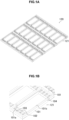
Fig. 1A is a perspective view showing the state of a package in a middle step so as to explain a manufacturing method of a package according to the first embodiment of the present invention; -
Fig. 1B is a perspective view showing the state of the package in a middle step so as to explain the manufacturing method of the package according to the first embodiment of the present invention; -
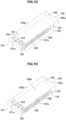
Fig. 1C is a perspective view showing the state of the package in a middle step so as to explain the manufacturing method of the package according to the first embodiment of the present invention; -
Fig. 1D is a perspective view showing the state of the package in a middle step so as to explain the manufacturing method of the package according to the first embodiment of the present invention; -
Fig. 1E is a perspective view showing the state of the package in a middle step so as to explain the manufacturing method of the package according to the first embodiment of the present invention; -
Fig. 1F is a perspective view showing the state of the package in a middle step so as to explain the manufacturing method of the package according to the first embodiment of the present invention; -
Fig. 1G is a perspective view showing the state of the package in a middle step so as to explain the manufacturing method of the package according to the first embodiment of the present invention; -
Fig. 1H is a perspective view showing the state of the package in a middle step so as to explain the manufacturing method of the package according to the first embodiment of the present invention; -
Fig. 1I is a perspective view showing the state of the package in a middle step so as to explain the manufacturing method of the package according to the first embodiment of the present invention; -
Fig. 1J is a perspective view showing the state of the package in a middle step so as to explain the manufacturing method of the package according to the first embodiment of the present invention; -
Fig. 2A is a perspective view showing the state of a package in a middle step so as to explain a manufacturing method of a package according to the second embodiment of the present invention; -
Fig. 2B is a perspective view showing the state of the package in a middle step so as to explain the manufacturing method of the package according to the second embodiment of the present invention; -
Fig. 2C is a perspective view showing the state of the package in a middle step so as to explain the manufacturing method of the package according to the second embodiment of the present invention; -
Fig. 2D is a perspective view showing the state of the package in a middle step so as to explain the manufacturing method of the package according to the second embodiment of the present invention; -
Fig. 2E is a perspective view showing the state of the package in a middle step so as to explain the manufacturing method of the package according to the second embodiment of the present invention; -
Fig. 2F is a perspective view showing the state of the package in a middle step so as to explain the manufacturing method of the package according to the second embodiment of the present invention; -
Fig. 2G is a perspective view showing the state of the package in a middle step so as to explain the manufacturing method of the package according to the second embodiment of the present invention; -
Fig. 2H is a perspective view showing the state of the package in a middle step so as to explain the manufacturing method of the package according to the second embodiment of the present invention; -
Fig. 21 is a perspective view showing the state of the package in a middle step so as to explain the manufacturing method of the package according to the second embodiment of the present invention; and -
Fig. 2J is a plan view showing the state of the package in a middle step so as to explain the manufacturing method of the package according to the second embodiment of the present invention. - A package according to an embodiment of the present invention and a manufacturing method of the same will be described below.
- A manufacturing method of a package according to the first embodiment of the present invention will be described first with reference to
Figs. 1A to 1J . - First, a first frame having an almost L shape in a planar view is produced (first step).
- For example, as shown in
Figs. 1A and 1B , anassembly 120 in which a plurality offrame assemblies 121 each forming twofirst frames 101 are integrated is produced. In theframe assembly 121, the twofirst frames 101 rotated by 180° with respect to each other in a planar view are integrated. - For example, a polyvinyl-based binder and a surfactant are added to powder (having an average particle size of, for example, 0.5 to 0.6 µm) of a predetermined metal oxide such as Al2O3, and these are dispersed in a dispersion medium made of an organic solvent such as 2-propanol, thereby producing a slurry. The produced slurry is molded by, for example, a well-known doctor blade method to form a layer of slurry, and the layer of slurry is dried by removing the dispersion medium from it, thereby forming a green sheet.
- On the other hand, a conductive paste in which fine particles of a metal such as tungsten are dispersed is applied, thereby producing a conductor layer sheet. On the conductor layer sheet, a paste pattern formed by the conductive paste and serving as a wiring pattern is formed.
- Next, a plurality of conductive sheets and green sheets are alternately stacked, thereby producing a multilayer sheet before sintering, which becomes the above-described
assembly 120. After that, the multilayer sheet is baked at a temperature of about 900°C to 1,000°C, thereby obtaining theassembly 120 that integrates a plurality offirst frames 101 in which a plurality of conductor layers and a plurality of insulating layers arranged between the plurality of conductor layers are stacked. - The thus produced
assembly 120 is divided into a plurality of parts, for example, as shown inFig. 1C , and each of the divided parts of theassembly 120 is divided into the frame assemblies 121 (Fig. 1D ). As a result, as shown inFig. 1E , thefirst frame 101 having an almost L shape in a planar view and including a first short side surface (side wall) 101a and a first long side surface (side wall) 101b can be produced. The firstshort side surface 101a and the firstlong side surface 101b are, for example, perpendicular to each other in a planar view. - In each
first frame 101, a plurality of conductor layers to which a plurality of DC electrode terminals are connected, and a plurality of insulating layers arranged between the plurality of conductor layers are stacked. The DC electrode terminal will be described later. In addition, a plurality of high-frequencyinternal terminals 103 are formed in an internalterminal portion 102 on the inner side of the firstshort side surface 101a. Also, in this example, eachfirst frame 101 includes a first joint 104 used to joint asecond frame 105 to be described later. In the first embodiment, when theframe assembly 121 is divided, twofirst frames 101 can be produced. Thefirst frame 101 is formed by a sintered body in which layers of ceramic and conductor layers are stacked. - Next, as shown in
Fig. 1F , thesecond frame 105 having an almost L shape in a planar view and including a second short side surface (side wall) 105a and a second long side surface (side wall) 105b is produced (second step). The secondshort side surface 105a and the secondlong side surface 105b are, for example, perpendicular to each other in a planar view. In this example, thesecond frame 105 includes a second joint 107 used to joint thefirst frame 101. In thesecond frame 105, the secondshort side surface 105a includes a throughhole 108. The throughhole 108 can be used as an optical signal input/output window for a high-frequency optical device stored (mounted) in the package. In addition, a plate-shapedbase material 106 serving as a floor portion is produced (third step). The floor portion will be described later. Thesecond frame 105 and thebase material 106 can be made of, for example, Kovar that is an alloy of iron, cobalt, and nickel. Kovar is an alloy having, as its characteristic, a linear expansion coefficient close to ceramic. In addition, from the viewpoint of heat dissipation of the high-frequency optical device mounted in the package, CuW that is an alloy of copper and tungsten is often used as thebase material 106. As a characteristic, CuW has a high thermal conductivity and a low linear expansion coefficient, and can be used as a peripheral material of ceramic or Kovar. - Next, as shown in
Fig. 1G , the plurality ofDC electrode terminals 109 are formed on the outer surface of the firstlong side surface 101b. Next, as shown inFig. 1H , thefirst frame 101, thesecond frame 105, and thebase material 106 are combined to form a package (fourth step). In this example, thefirst joint 104 of thefirst frame 101 and thesecond joint 107 of thesecond frame 105 are tenon-jointed, thereby combining thefirst frame 101 and thesecond frame 105. Although tenon joint is used in this example, permanent connection of planes using silver solder or the like can also be implemented, as a matter of course. For example, a first joint surface is provided in the joint portion of thefirst frame 101 to thesecond frame 105 and a second joint surface is provided in the joint portion of thesecond frame 105 to thefirst frame 101. The first joint surface and the second joint surface are permanently jointed, thereby combining thefirst frame 101 and thesecond frame 105. - The package includes a
rectangular floor portion 106a including a long side and a short side, the firstshort side surface 101a and the secondshort side surface 105a arranged on the portions of the short sides of thefloor portion 106a, and the firstlong side surface 101b and the secondlong side surface 105b arranged on the portions of the long sides of thefloor portion 106a. The firstshort side surface 101a and the secondshort side surface 105a are arranged on the portions of the two short sides of thefloor portion 106a, which are in an opposite position to each other. The firstlong side surface 101b and the secondlong side surface 105b are arranged on the portions of the two long sides of thefloor portion 106a, which are in an opposite position to each other. - Also, the package includes the plurality of high-frequency
internal terminals 103 arrayed in the internalterminal portion 102 on the inner side of the firstshort side surface 101a and connected to the high-frequency optical device mounted inside. In addition, the package includes a plurality of high-frequency external terminals (not shown) arrayed in a first external terminal portion on the outer side of thefloor portion 106a on the side of the firstshort side surface 101a and connected to the high-frequencyinternal terminals 103 and connected to lead pins. In addition, the package includes the plurality ofDC electrode terminals 109 arrayed in a second external terminal portion on the outer side of the firstlong side surface 101b. - Here, the package is formed by the
first frame 101 having an almost L shape in a planar view, thesecond frame 105 having an almost L shape in a planar view, and thebase material 106 serving as thefloor portion 106a, as described above. Thefirst frame 101 includes the portions of the firstshort side surface 101a and the firstlong side surface 101b, in which a plurality of conductor layers to which the plurality ofDC electrode terminals 109 are connected, and a plurality of insulating layers arranged between the plurality of conductor layers are stacked. On the other hand, thesecond frame 105 includes the portions of the secondshort side surface 105a and the secondlong side surface 105b, and does not have a structure including alternately stacked insulating layers and conductor layers. - Also, in this example, the
first frame 101 includes the first joint 104 provided in the joint portion to thesecond frame 105, thesecond frame 105 includes the second joint 107 provided in the joint portion to thefirst frame 101, and thefirst joint 104 of thefirst frame 101 and thesecond joint 107 of thesecond frame 105 are tenon-jointed. Although tenon joint is used in this example, permanent connection of planes using silver solder or the like can also be implemented, as described above, as a matter of course. - In the package according to the first embodiment, a high-frequency optical device or an optical component can be mounted in a bathtub structure on the
floor portion 106a surrounded by thefirst frame 101 and thesecond frame 105. - Note that as shown in
Figs. 1I and 1J , DC lead pins 110 are connected to the plurality ofDC electrode terminals 109. In addition, a plurality of high-frequencyexternal terminals 112 are arrayed in a firstexternal terminal portion 111 on the outer side of thefloor portion 106a on the side of the firstshort side surface 101a, and RF lead pins 113 are connected to the plurality of high-frequencyexternal terminals 112. - As described above, according to the first embodiment, the multilayer structure of the plurality of conductor layers and the plurality of insulating layers is formed only in the portion of the first frame. It is therefore possible to manufacture a package of CDM at a lower cost.
- A manufacturing method of a package according to the second embodiment of the present invention will be described next with reference to
Figs. 2A to 2J . - First, a first frame having an almost L shape in a planar view is produced (first step).
- For example, as shown in
Figs. 2A and2 , anassembly 120a in which a plurality offrame assemblies 121a each forming a plurality of first frames 101' are integrated is produced. In theframe assembly 121a, the plurality of first frames 101' are stacked and integrally connected by connectingportions 122 while holding such a positional relationship that the first frames are translated in the direction of the long side of the package in a planar view such that an internalterminal portion 102 is visible from the outside. - For example, a polyvinyl-based binder and a surfactant are added to powder of a predetermined metal oxide such as Al2O3, and these are dispersed in a dispersion medium, thereby producing a slurry. The produced slurry is molded to form a layer of slurry, and the layer of slurry is dried by removing the dispersion medium from it, thereby forming a green sheet.
- On the other hand, a conductive paste in which fine particles of a metal such as tungsten are dispersed is applied, thereby producing a conductor layer sheet. On the conductor layer sheet, a paste pattern formed by the conductive paste and serving as a wiring pattern is formed.
- Next, a plurality of conductive sheets and green sheets are alternately stacked, thereby producing a multilayer sheet before sintering, which becomes the above-described
assembly 120a. After that, the multilayer sheet is baked at a temperature of about 900°C to 1,000°C, thereby obtaining theassembly 120a in which a plurality of first frame 101', which are formed by stacking a plurality of conductor layers and a plurality of insulating layers arranged between the plurality of conductor layers, are connected by the connectingportions 122 and integrated. - The thus produced
assembly 120a is divided into a plurality of parts, for example, as shown inFig. 2C , and each of the divided parts of theassembly 120a is divided into theframe assemblies 121a by separating the connecting portions 122 (Fig. 2D ). As a result, as shown inFig. 2E , the first frame 101' having an almost L shape in a planar view can be produced. The first frame 101' is formed by a sintered body in which layers of ceramic and conductor layers are stacked. - Next, as shown in
Fig. 2F , a second frame 105' having an almost L shape in a planar view and including a secondshort side surface 105a, a secondlong side surface 105b, and aspacer 114 is produced (second step). The secondshort side surface 105a and the secondlong side surface 105b are, for example, perpendicular to each other in a planar view. In this example, the second frame 105' includes a second joint 107 used to joint the first frame 101'. Also, in the second frame 105', the secondshort side surface 105a includes a throughhole 108. The throughhole 108 can be used as an optical signal input/output window for an optical module stored (mounted) in the package. Note that thespacer 114 and the second frame 105' can be integrated, or can be formed separately. - In addition, a plate-shaped
base material 106 serving as a floor portion is produced (third step). In the second embodiment, thebase material 106 includes aflange 115 as a thin flat projection structure. The second frame 105', thespacer 114, and thebase material 106 can be made of, for example, an alloy of Kovar and nickel. In addition, from the viewpoint of heat dissipation, thebase material 106 can also be made of an alloy of copper and tungsten. Theflange 115 is not limited to one, and a plurality of flanges can be provided on the side of the second short side surface and the side of the second long side of thebase material 106 in a state in which the flanges match the bottom surface position of thebase material 106. - Next, as shown in
Fig. 2G , a plurality ofDC electrode terminals 109 are formed on the outer surface of the firstlong side surface 101b. Here, theframe assembly 121a includes the portions of a firstshort side surface 101a and a firstlong side surface 101b, and the firstshort side surface 101a and the firstlong side surface 101b are, for example, perpendicular to each other in a planar view. - In the first frame 101', a plurality of conductor layers to which the plurality of
DC electrode terminals 109 are connected, and a plurality of insulating layers arranged between the plurality of conductor layers are stacked. In addition, a plurality of high-frequencyinternal terminals 103 are formed in the internalterminal portion 102 on the inner side of the firstshort side surface 101a. Also, in this example, each first frame 101' includes a first joint 104 used to joint the second frame 105' to be described later. - Next, as shown in
Figs. 2H and2 , the first frame 101', the second frame 105', thebase material 106, and thespacer 114 are combined to form a package (fourth step). In this example, thefirst joint 104 of the first frame 101' and thesecond joint 107 of the second frame 105' are tenon-jointed, thereby combining the first frame 101' and the second frame 105'. Also, in this example, thespacer 114 is arranged between the internalterminal portion 102 and thebase material 106. - In addition, a conductor layer is formed on the lower surface of the internal
terminal portion 102, which thespacer 114 contacts, and these can be rendered conductive. Hence, the internalterminal portion 102 is provided with a plurality of Grounded-GSSG differential high-frequency line ends (high-frequency internal terminals 103), and the line ends and an electronic device mounted inside are electrically connected to each other to propagate a high-frequency signal. Since thespacer 114 and the ground conductor thin film surface inside the package are electrically connected, the ground potential that forms the GSSG differential high-frequency line ends can reliably match the package ground, and it is expected that the high-frequency characteristic of the package can stably be obtained. More specifically, this contributes to reduction of crosstalk between the plurality of GSSG differential high-frequency lines. - Here, the package includes a
rectangular floor portion 106a including a long side and a short side, the firstshort side surface 101a and the secondshort side surface 105a arranged on the portions of the short sides of thefloor portion 106a, and the firstlong side surface 101b and the secondlong side surface 105b arranged on the portions of the long sides of thefloor portion 106a. The firstshort side surface 101a and the secondshort side surface 105a are arranged on the portions of the two short sides of thefloor portion 106a, which are in an opposite position to each other. The firstlong side surface 101b and the secondlong side surface 105b are arranged on the portions of the two long sides of thefloor portion 106a, which are in an opposite position to each other. - Also, the package includes the plurality of high-frequency
internal terminals 103 arrayed in the internalterminal portion 102 on the inner side of the firstshort side surface 101a and connected to the stored element. In addition, the package includes a plurality of high-frequency external terminals (not shown) arrayed in a first external terminal portion on the outer side of thefloor portion 106a on the side of the firstshort side surface 101a and connected to the high-frequencyinternal terminals 103 and connected to lead pins. In addition, the package includes the plurality ofDC electrode terminals 109 arrayed in a second external terminal portion on the outer side of the firstlong side surface 101b. - As described above, in the first frame 101' of package, a plurality of conductor layers to which the plurality of
DC electrode terminals 109 are connected, and a plurality of insulating layers arranged between the plurality of conductor layers are stacked, as in the above-described first embodiment. On the other hand, the second frame 105' includes the portions of the secondshort side surface 105a and the secondlong side surface 105b, and does not have a structure including alternately stacked insulating layers and conductor layers. - In the package according to the second embodiment as well, a high-frequency optical device or an optical component can be mounted in a bathtub structure on the
floor portion 106a surrounded by the first frame 101' and the second frame 105', as in the above-described first embodiment. - Note that as shown in
Fig. 2J , DC lead pins 110 are connected to the plurality ofDC electrode terminals 109. In addition, a plurality of high-frequencyexternal terminals 112 are arrayed in a firstexternal terminal portion 111 on the outer side of thefloor portion 106a on the side of the firstshort side surface 101a, and RF lead pins 113 are connected to the plurality of high-frequencyexternal terminals 112. - As described above, according to the second embodiment, the multilayer structure of the plurality of conductor layers and the plurality of insulating layers is formed only in the portion of the first frame. It is therefore possible to manufacture a package of CDM at a lower cost.
- Also, in the second embodiment, the
base material 106 includes theflange 115. It is therefore possible to suppress generation of a stress load on the lead pins and solder when mounting the package on a mounting board to mount it. - For example, when an optical module including a high-frequency optical device or an optical component mounted in the package is mounted on a mounting board, solder mounting is performed in general. RF lead pins or DC lead pins are fixed on the mounting board by solder. Generally, the linear expansion coefficient of the mounting board is larger than that of the package. For this reason, if the mounting board thermally expands or shrinks along with a change of the environmental temperature, a stress load to the lead pins and the solder that fixes the lead pins is generated in an area where the solder mounting density of the lead pins is relatively low. In the worst case, these are ruptured to make the RF lead pins open, and propagation of a high-frequency signal is impeded.
- Against the above-described problem, the flange integrated with the base material is used. When the flange is connected and fixed to the mounting board by solder or the like, generation of the above-described stress load can be suppressed. Hence, the RF lead pins can be prevented from being open, and an optical module that is stable against the change of the environmental temperature can be provided.
- As described above, according to the present invention, since the multilayer structure of the plurality of conductor layers and the plurality of insulating layers forms the portion of the first frame, a package of CDM can be manufactured at a lower cost.
- Note that the present invention is not limited to the above-described embodiments, and it is obvious that many modifications and combinations can be made by a person skilled in the art in this field within the technical scope of the present invention.
- 101...first frame, 101a...first short side surface, 101b...first long side surface, 102...internal terminal portion, 103...high-frequency internal terminal, 104...first joint, 105...second frame, 105a...second short side surface, 105b...second long side surface, 106...base material, 107...second joint, 108...through hole, 109...DC electrode terminal, 110...DC lead pin, 111...first external terminal portion, 112...high-frequency external terminal, 113...RF lead pin, 120...assembly, 121...frame assembly.
Claims (12)
- A manufacturing method of a package including:a rectangular floor portion including a long side and a short side, a first short side surface and a second short side surface arranged on respective portions of two short sides of the floor portion, which are in an opposite position to each other, and a first long side surface and a second long side surface arranged on respective portions of two long sides of the floor portion, which are in an opposite position to each other;a plurality of high-frequency internal terminals arrayed in an internal terminal portion on an inner side of the first short side surface and connected to a high-frequency optical device mounted inside;a plurality of high-frequency external terminals arrayed in a first external terminal portion on an outer side of the floor portion on an outer side of the first short side surface and connected to the internal terminals and connected to lead pins; anda plurality of DC electrode terminals arrayed in a second external terminal portion on an outer side of the first long side surface,the method comprising:a first step of producing a first frame having an almost L shape in a planar view and including portions of the first short side surface and the first long side surface, in which a plurality of conductor layers to which the plurality of DC electrode terminals are connected, and a plurality of insulating layers arranged between the plurality of conductor layers are stacked;a second step of producing a second frame having an almost L shape in a planar view and including portions of the second short side surface and the second long side surface;a third step of producing a plate-shaped base material serving as the floor portion; anda fourth step of combining the first frame, the second frame, and the base material to form the package.
- The manufacturing method of the package according to claim 1, wherein
in the first step, a frame assembly in which two first frames rotated by 180° with respect to each other in a planar view are integrated is produced, and the frame assembly is divided into the two first frames, thereby producing the first frame. - The manufacturing method of the package according to claim 1, wherein
in the first step, a frame assembly is produced in which the plurality of first frames are stacked and integrated by connecting portions while holding such a positional relationship that the first frames are translated in a direction of the long side of the package in a planar view such that the internal terminal portion is visible from the outside, and the connecting portions are removed to divide the frame assembly into the first frames, thereby producing the first frame. - The manufacturing method of the package according to claim 2 or 3, wherein
in the first step, an assembly in which a plurality of frame assemblies are integrated is produced, and the assembly is divided into the frame assemblies, thereby producing the frame assembly. - The manufacturing method of the package according to any one of claims 1 to 4, wherein
in the fourth step, the first frame, the second frame, the base material, and a spacer arranged between the internal terminal portion and the base material are combined to form the package. - The manufacturing method of the package according to claim 5, wherein
the spacer is integrated with the second frame. - The manufacturing method of the package according to any one of claims 1 to 6, whereinthe first frame includes one of a first joint and a first joint surface provided in a joint portion to the second frame,the second frame includes one of a second joint and a second joint surface provided in a joint portion to the first frame, andin the fourth step, the first joint of the first frame and the second joint of the second frame are tenon-jointed, or the first joint surface of the first frame and the second joint surface of the second frame are permanently jointed, thereby combining the first frame and the second frame.
- The manufacturing method of the package according to any one of claims 1 to 7, wherein
the base material comprises, on a side of the second short side surface and a side of a second long side, at least one thin flat projection structure that matches a bottom surface position of the base material. - A package comprising:a rectangular floor portion including a long side and a short side, a first short side surface and a second short side surface arranged on respective portions of two short sides of the floor portion, which are in an opposite position to each other, and a first long side surface and a second long side surface arranged on respective portions of two long sides of the floor portion, which are in an opposite position to each other;a plurality of high-frequency internal terminals arrayed in an internal terminal portion on an inner side of the first short side surface and connected to a high-frequency optical device mounted inside;a plurality of high-frequency external terminals arrayed in a first external terminal portion on an outer side of the floor portion on an outer side of the first short side surface and connected to the internal terminals and connected to lead pins; anda plurality of DC electrode terminals arrayed in a second external terminal portion on an outer side of the first long side surface, characterized by comprising:a first frame having an almost L shape in a planar view and including portions of the first short side surface and the first long side surface, in which a plurality of conductor layers to which the plurality of DC electrode terminals are connected, and a plurality of insulating layers arranged between the plurality of conductor layers are stacked;a second frame having an almost L shape in a planar view and including portions of the second short side surface and the second long side surface; anda plate-shaped base material serving as the floor portion.
- The package according to claim 9, characterized by further comprising
a spacer arranged between the internal terminal portion and the base material. - The package according to claim 10,
wherein
the spacer is integrated with the second frame. - The package according to any one of
claims 9 to 11, whereinthe first frame includes one of a first joint and a first joint surface provided in a joint portion to the second frame,the second frame includes one of a second joint and a second joint surface provided in a joint portion to the first frame, andthe first joint of the first frame and the second joint of the second frame are tenon-jointed, or the first joint surface of the first frame and the second joint surface of the second frame are permanently jointed.
Applications Claiming Priority (1)
| Application Number | Priority Date | Filing Date | Title |
|---|---|---|---|
| PCT/JP2020/029665 WO2022029838A1 (en) | 2020-08-03 | 2020-08-03 | Package and production method therefor |
Publications (3)
| Publication Number | Publication Date |
|---|---|
| EP4191657A1 true EP4191657A1 (en) | 2023-06-07 |
| EP4191657A4 EP4191657A4 (en) | 2024-05-01 |
| EP4191657B1 EP4191657B1 (en) | 2025-10-01 |
Family
ID=80117163
Family Applications (1)
| Application Number | Title | Priority Date | Filing Date |
|---|---|---|---|
| EP20948557.2A Active EP4191657B1 (en) | 2020-08-03 | 2020-08-03 | Package and production method therefor |
Country Status (5)
| Country | Link |
|---|---|
| US (1) | US12322668B2 (en) |
| EP (1) | EP4191657B1 (en) |
| JP (1) | JP7207602B2 (en) |
| CN (1) | CN114503251B (en) |
| WO (1) | WO2022029838A1 (en) |
Families Citing this family (1)
| Publication number | Priority date | Publication date | Assignee | Title |
|---|---|---|---|---|
| JP7803192B2 (en) * | 2022-03-30 | 2026-01-21 | 住友大阪セメント株式会社 | Optical device and optical transmitter using the same |
Family Cites Families (13)
| Publication number | Priority date | Publication date | Assignee | Title |
|---|---|---|---|---|
| JP2005317830A (en) * | 2004-04-30 | 2005-11-10 | Elpida Memory Inc | Semiconductor device, multichip package, and wire bonding method |
| WO2012043313A1 (en) * | 2010-09-28 | 2012-04-05 | 京セラ株式会社 | Element housing package, and electronic device using the same |
| JP6075597B2 (en) * | 2012-06-28 | 2017-02-08 | 京セラ株式会社 | Device storage package and mounting structure |
| JP6030371B2 (en) * | 2012-07-27 | 2016-11-24 | 京セラ株式会社 | Device storage package and mounting structure |
| CN204303794U (en) * | 2012-10-30 | 2015-04-29 | 京瓷株式会社 | Package for storing components and mounting structure |
| WO2015029880A1 (en) * | 2013-08-28 | 2015-03-05 | 京セラ株式会社 | Package for housing elements and mounting structure |
| CN105144370B (en) * | 2013-09-25 | 2017-11-14 | 京瓷株式会社 | Electronic unit storage packaging part and electronic installation |
| WO2015088028A1 (en) * | 2013-12-13 | 2015-06-18 | 京セラ株式会社 | Element housing package and mounting structure |
| US20190057959A1 (en) * | 2015-06-06 | 2019-02-21 | Monolithic 3D Inc. | Semiconductor device and structure with thermal isolation |
| JP2017117899A (en) * | 2015-12-22 | 2017-06-29 | Ngkエレクトロデバイス株式会社 | Package for housing electronic component |
| JP6853034B2 (en) * | 2015-12-25 | 2021-03-31 | 京セラ株式会社 | Optical semiconductor device storage package and optical semiconductor device |
| JP2018164040A (en) * | 2017-03-27 | 2018-10-18 | 東芝メモリ株式会社 | Semiconductor device |
| TWI672791B (en) * | 2018-05-07 | 2019-09-21 | 財團法人工業技術研究院 | Chip package structure and manufacturing method thereof |
-
2020
- 2020-08-03 JP JP2022502117A patent/JP7207602B2/en active Active
- 2020-08-03 EP EP20948557.2A patent/EP4191657B1/en active Active
- 2020-08-03 CN CN202080068689.5A patent/CN114503251B/en active Active
- 2020-08-03 US US17/765,662 patent/US12322668B2/en active Active
- 2020-08-03 WO PCT/JP2020/029665 patent/WO2022029838A1/en not_active Ceased
Also Published As
| Publication number | Publication date |
|---|---|
| CN114503251A (en) | 2022-05-13 |
| WO2022029838A1 (en) | 2022-02-10 |
| EP4191657B1 (en) | 2025-10-01 |
| JP7207602B2 (en) | 2023-01-18 |
| US12322668B2 (en) | 2025-06-03 |
| EP4191657A4 (en) | 2024-05-01 |
| CN114503251B (en) | 2025-07-29 |
| US20220384285A1 (en) | 2022-12-01 |
| JPWO2022029838A1 (en) | 2022-02-10 |
Similar Documents
| Publication | Publication Date | Title |
|---|---|---|
| CN108022899B (en) | Power module having lead member and method of manufacturing the same | |
| CN100429841C (en) | transport connector | |
| US20200375034A1 (en) | Electronic component mounting structure and method | |
| CN113555332B (en) | A high frequency device integrated module and module | |
| CN111630728B (en) | Surface mount connector and surface mount connector set | |
| CN107924880A (en) | Electronic component mounting package and electronic device | |
| JP6633656B2 (en) | Wiring board, optical semiconductor element package and optical semiconductor device | |
| WO2023145651A1 (en) | Wiring board, electronic component mounting package using wiring board, and electronic module | |
| EP4191657B1 (en) | Package and production method therefor | |
| CN105322330A (en) | Dual thickness double-ended male blade terminal | |
| EP3098842B1 (en) | Package for an electronic element | |
| JP3680792B2 (en) | Multi-connector for high-speed communication apparatus and mounting method of multi-connector for high-speed communication apparatus and printed circuit board | |
| CN218213543U (en) | Input and output components and packaging bases and optical devices | |
| CN110337718B (en) | Insulating substrate, semiconductor package, and semiconductor device | |
| CN113785450A (en) | Electrical connector system with differential pair cable interface | |
| CN114696161B (en) | Lead wire module, electric connector and connector assembly | |
| JP2001257415A (en) | Optical semiconductor device | |
| CN115343812B (en) | Input/output component, preparation method, package base and optical device | |
| TW202135376A (en) | Radio frequency (rf) energy transmission line transition structure | |
| CN216015646U (en) | Filter and communication base station | |
| JP2000049509A (en) | Wiring board and its connection structure | |
| JP2013046041A (en) | Signal transmission line | |
| WO2015029880A1 (en) | Package for housing elements and mounting structure | |
| JP3628254B2 (en) | Package for storing semiconductor elements | |
| JP2661004B2 (en) | Dielectric filter |
Legal Events
| Date | Code | Title | Description |
|---|---|---|---|
| STAA | Information on the status of an ep patent application or granted ep patent |
Free format text: STATUS: THE INTERNATIONAL PUBLICATION HAS BEEN MADE |
|
| PUAI | Public reference made under article 153(3) epc to a published international application that has entered the european phase |
Free format text: ORIGINAL CODE: 0009012 |
|
| STAA | Information on the status of an ep patent application or granted ep patent |
Free format text: STATUS: REQUEST FOR EXAMINATION WAS MADE |
|
| 17P | Request for examination filed |
Effective date: 20220324 |
|
| AK | Designated contracting states |
Kind code of ref document: A1 Designated state(s): AL AT BE BG CH CY CZ DE DK EE ES FI FR GB GR HR HU IE IS IT LI LT LU LV MC MK MT NL NO PL PT RO RS SE SI SK SM TR |
|
| DAV | Request for validation of the european patent (deleted) | ||
| DAX | Request for extension of the european patent (deleted) | ||
| A4 | Supplementary search report drawn up and despatched |
Effective date: 20240328 |
|
| RIC1 | Information provided on ipc code assigned before grant |
Ipc: H01L 23/66 20060101ALI20240322BHEP Ipc: H01L 23/057 20060101ALI20240322BHEP Ipc: G02B 6/42 20060101ALI20240322BHEP Ipc: H01L 31/02 20060101ALI20240322BHEP Ipc: H01L 23/12 20060101ALI20240322BHEP Ipc: H01L 23/02 20060101AFI20240322BHEP |
|
| RIC1 | Information provided on ipc code assigned before grant |
Ipc: H10F 77/00 20250101ALI20250130BHEP Ipc: H01L 23/66 20060101ALI20250130BHEP Ipc: H01L 23/057 20060101ALI20250130BHEP Ipc: G02B 6/42 20060101ALI20250130BHEP Ipc: H01L 23/12 20060101ALI20250130BHEP Ipc: H01L 23/02 20060101AFI20250130BHEP |
|
| GRAP | Despatch of communication of intention to grant a patent |
Free format text: ORIGINAL CODE: EPIDOSNIGR1 |
|
| STAA | Information on the status of an ep patent application or granted ep patent |
Free format text: STATUS: GRANT OF PATENT IS INTENDED |
|
| INTG | Intention to grant announced |
Effective date: 20250321 |
|
| RAP3 | Party data changed (applicant data changed or rights of an application transferred) |
Owner name: NIPPON TELEGRAPH AND TELEPHONE CORPORATION |
|
| GRAS | Grant fee paid |
Free format text: ORIGINAL CODE: EPIDOSNIGR3 |
|
| GRAA | (expected) grant |
Free format text: ORIGINAL CODE: 0009210 |
|
| STAA | Information on the status of an ep patent application or granted ep patent |
Free format text: STATUS: THE PATENT HAS BEEN GRANTED |
|
| AK | Designated contracting states |
Kind code of ref document: B1 Designated state(s): AL AT BE BG CH CY CZ DE DK EE ES FI FR GB GR HR HU IE IS IT LI LT LU LV MC MK MT NL NO PL PT RO RS SE SI SK SM TR |
|
| RAP3 | Party data changed (applicant data changed or rights of an application transferred) |
Owner name: NTT, INC. |
|
| REG | Reference to a national code |
Ref country code: GB Ref legal event code: FG4D Ref country code: CH Ref legal event code: F10 Free format text: ST27 STATUS EVENT CODE: U-0-0-F10-F00 (AS PROVIDED BY THE NATIONAL OFFICE) Effective date: 20251001 |
|
| REG | Reference to a national code |
Ref country code: IE Ref legal event code: FG4D |
|
| REG | Reference to a national code |
Ref country code: DE Ref legal event code: R096 Ref document number: 602020059973 Country of ref document: DE |
|
| REG | Reference to a national code |
Ref country code: DE Ref legal event code: R079 Ref document number: 602020059973 Country of ref document: DE Free format text: PREVIOUS MAIN CLASS: H01L0023020000 Ipc: H10W0076100000 |
|
| REG | Reference to a national code |
Ref country code: NL Ref legal event code: MP Effective date: 20251001 |
|
| REG | Reference to a national code |
Ref country code: AT Ref legal event code: MK05 Ref document number: 1843476 Country of ref document: AT Kind code of ref document: T Effective date: 20251001 |
|
| PG25 | Lapsed in a contracting state [announced via postgrant information from national office to epo] |
Ref country code: NL Free format text: LAPSE BECAUSE OF FAILURE TO SUBMIT A TRANSLATION OF THE DESCRIPTION OR TO PAY THE FEE WITHIN THE PRESCRIBED TIME-LIMIT Effective date: 20251001 |
|
| PG25 | Lapsed in a contracting state [announced via postgrant information from national office to epo] |
Ref country code: ES Free format text: LAPSE BECAUSE OF FAILURE TO SUBMIT A TRANSLATION OF THE DESCRIPTION OR TO PAY THE FEE WITHIN THE PRESCRIBED TIME-LIMIT Effective date: 20251001 |
|
| REG | Reference to a national code |
Ref country code: LT Ref legal event code: MG9D |
|
| PG25 | Lapsed in a contracting state [announced via postgrant information from national office to epo] |
Ref country code: NO Free format text: LAPSE BECAUSE OF FAILURE TO SUBMIT A TRANSLATION OF THE DESCRIPTION OR TO PAY THE FEE WITHIN THE PRESCRIBED TIME-LIMIT Effective date: 20260101 |
|
| PG25 | Lapsed in a contracting state [announced via postgrant information from national office to epo] |
Ref country code: AT Free format text: LAPSE BECAUSE OF FAILURE TO SUBMIT A TRANSLATION OF THE DESCRIPTION OR TO PAY THE FEE WITHIN THE PRESCRIBED TIME-LIMIT Effective date: 20251001 Ref country code: HR Free format text: LAPSE BECAUSE OF FAILURE TO SUBMIT A TRANSLATION OF THE DESCRIPTION OR TO PAY THE FEE WITHIN THE PRESCRIBED TIME-LIMIT Effective date: 20251001 Ref country code: FI Free format text: LAPSE BECAUSE OF FAILURE TO SUBMIT A TRANSLATION OF THE DESCRIPTION OR TO PAY THE FEE WITHIN THE PRESCRIBED TIME-LIMIT Effective date: 20251001 |
|
| PG25 | Lapsed in a contracting state [announced via postgrant information from national office to epo] |
Ref country code: RS Free format text: LAPSE BECAUSE OF FAILURE TO SUBMIT A TRANSLATION OF THE DESCRIPTION OR TO PAY THE FEE WITHIN THE PRESCRIBED TIME-LIMIT Effective date: 20260101 |
|
| PG25 | Lapsed in a contracting state [announced via postgrant information from national office to epo] |
Ref country code: IS Free format text: LAPSE BECAUSE OF FAILURE TO SUBMIT A TRANSLATION OF THE DESCRIPTION OR TO PAY THE FEE WITHIN THE PRESCRIBED TIME-LIMIT Effective date: 20260201 |
|
| PG25 | Lapsed in a contracting state [announced via postgrant information from national office to epo] |
Ref country code: CZ Free format text: LAPSE BECAUSE OF FAILURE TO SUBMIT A TRANSLATION OF THE DESCRIPTION OR TO PAY THE FEE WITHIN THE PRESCRIBED TIME-LIMIT Effective date: 20251001 Ref country code: PT Free format text: LAPSE BECAUSE OF FAILURE TO SUBMIT A TRANSLATION OF THE DESCRIPTION OR TO PAY THE FEE WITHIN THE PRESCRIBED TIME-LIMIT Effective date: 20260202 |
|
| PG25 | Lapsed in a contracting state [announced via postgrant information from national office to epo] |
Ref country code: PL Free format text: LAPSE BECAUSE OF FAILURE TO SUBMIT A TRANSLATION OF THE DESCRIPTION OR TO PAY THE FEE WITHIN THE PRESCRIBED TIME-LIMIT Effective date: 20251001 |
|
| PG25 | Lapsed in a contracting state [announced via postgrant information from national office to epo] |
Ref country code: LV Free format text: LAPSE BECAUSE OF FAILURE TO SUBMIT A TRANSLATION OF THE DESCRIPTION OR TO PAY THE FEE WITHIN THE PRESCRIBED TIME-LIMIT Effective date: 20251001 |
|
| PG25 | Lapsed in a contracting state [announced via postgrant information from national office to epo] |
Ref country code: BG Free format text: LAPSE BECAUSE OF FAILURE TO SUBMIT A TRANSLATION OF THE DESCRIPTION OR TO PAY THE FEE WITHIN THE PRESCRIBED TIME-LIMIT Effective date: 20251001 |