EP4190937A1 - Deposition apparatus for organic light-emitting diode - Google Patents
Deposition apparatus for organic light-emitting diode Download PDFInfo
- Publication number
- EP4190937A1 EP4190937A1 EP21895094.7A EP21895094A EP4190937A1 EP 4190937 A1 EP4190937 A1 EP 4190937A1 EP 21895094 A EP21895094 A EP 21895094A EP 4190937 A1 EP4190937 A1 EP 4190937A1
- Authority
- EP
- European Patent Office
- Prior art keywords
- emitting diode
- auxiliary chamber
- organic light
- light emitting
- deposition apparatus
- Prior art date
- Legal status (The legal status is an assumption and is not a legal conclusion. Google has not performed a legal analysis and makes no representation as to the accuracy of the status listed.)
- Pending
Links
- 230000008021 deposition Effects 0.000 title claims abstract description 84
- 239000000463 material Substances 0.000 claims abstract description 46
- 238000000151 deposition Methods 0.000 claims description 85
- 238000010438 heat treatment Methods 0.000 claims description 36
- 230000006835 compression Effects 0.000 claims description 5
- 238000007906 compression Methods 0.000 claims description 5
- 238000011156 evaluation Methods 0.000 abstract description 5
- 238000004904 shortening Methods 0.000 abstract description 5
- 238000000034 method Methods 0.000 description 11
- 239000000758 substrate Substances 0.000 description 8
- 239000010409 thin film Substances 0.000 description 6
- 238000001704 evaporation Methods 0.000 description 5
- 239000011368 organic material Substances 0.000 description 5
- 230000008020 evaporation Effects 0.000 description 4
- 239000002994 raw material Substances 0.000 description 4
- 239000000470 constituent Substances 0.000 description 3
- 230000000694 effects Effects 0.000 description 2
- 239000010408 film Substances 0.000 description 2
- 238000004519 manufacturing process Methods 0.000 description 2
- 238000012986 modification Methods 0.000 description 2
- 230000004048 modification Effects 0.000 description 2
- 239000004020 conductor Substances 0.000 description 1
- 238000005286 illumination Methods 0.000 description 1
- 239000012535 impurity Substances 0.000 description 1
- 238000005259 measurement Methods 0.000 description 1
- 239000007921 spray Substances 0.000 description 1
- 238000005507 spraying Methods 0.000 description 1
- 238000002207 thermal evaporation Methods 0.000 description 1
- 238000012546 transfer Methods 0.000 description 1
- 238000013022 venting Methods 0.000 description 1
Images


Classifications
-
- C—CHEMISTRY; METALLURGY
- C23—COATING METALLIC MATERIAL; COATING MATERIAL WITH METALLIC MATERIAL; CHEMICAL SURFACE TREATMENT; DIFFUSION TREATMENT OF METALLIC MATERIAL; COATING BY VACUUM EVAPORATION, BY SPUTTERING, BY ION IMPLANTATION OR BY CHEMICAL VAPOUR DEPOSITION, IN GENERAL; INHIBITING CORROSION OF METALLIC MATERIAL OR INCRUSTATION IN GENERAL
- C23C—COATING METALLIC MATERIAL; COATING MATERIAL WITH METALLIC MATERIAL; SURFACE TREATMENT OF METALLIC MATERIAL BY DIFFUSION INTO THE SURFACE, BY CHEMICAL CONVERSION OR SUBSTITUTION; COATING BY VACUUM EVAPORATION, BY SPUTTERING, BY ION IMPLANTATION OR BY CHEMICAL VAPOUR DEPOSITION, IN GENERAL
- C23C14/00—Coating by vacuum evaporation, by sputtering or by ion implantation of the coating forming material
- C23C14/22—Coating by vacuum evaporation, by sputtering or by ion implantation of the coating forming material characterised by the process of coating
- C23C14/24—Vacuum evaporation
-
- C—CHEMISTRY; METALLURGY
- C23—COATING METALLIC MATERIAL; COATING MATERIAL WITH METALLIC MATERIAL; CHEMICAL SURFACE TREATMENT; DIFFUSION TREATMENT OF METALLIC MATERIAL; COATING BY VACUUM EVAPORATION, BY SPUTTERING, BY ION IMPLANTATION OR BY CHEMICAL VAPOUR DEPOSITION, IN GENERAL; INHIBITING CORROSION OF METALLIC MATERIAL OR INCRUSTATION IN GENERAL
- C23C—COATING METALLIC MATERIAL; COATING MATERIAL WITH METALLIC MATERIAL; SURFACE TREATMENT OF METALLIC MATERIAL BY DIFFUSION INTO THE SURFACE, BY CHEMICAL CONVERSION OR SUBSTITUTION; COATING BY VACUUM EVAPORATION, BY SPUTTERING, BY ION IMPLANTATION OR BY CHEMICAL VAPOUR DEPOSITION, IN GENERAL
- C23C14/00—Coating by vacuum evaporation, by sputtering or by ion implantation of the coating forming material
- C23C14/22—Coating by vacuum evaporation, by sputtering or by ion implantation of the coating forming material characterised by the process of coating
- C23C14/24—Vacuum evaporation
- C23C14/243—Crucibles for source material
-
- B—PERFORMING OPERATIONS; TRANSPORTING
- B01—PHYSICAL OR CHEMICAL PROCESSES OR APPARATUS IN GENERAL
- B01B—BOILING; BOILING APPARATUS ; EVAPORATION; EVAPORATION APPARATUS
- B01B1/00—Boiling; Boiling apparatus for physical or chemical purposes ; Evaporation in general
- B01B1/005—Evaporation for physical or chemical purposes; Evaporation apparatus therefor, e.g. evaporation of liquids for gas phase reactions
-
- C—CHEMISTRY; METALLURGY
- C23—COATING METALLIC MATERIAL; COATING MATERIAL WITH METALLIC MATERIAL; CHEMICAL SURFACE TREATMENT; DIFFUSION TREATMENT OF METALLIC MATERIAL; COATING BY VACUUM EVAPORATION, BY SPUTTERING, BY ION IMPLANTATION OR BY CHEMICAL VAPOUR DEPOSITION, IN GENERAL; INHIBITING CORROSION OF METALLIC MATERIAL OR INCRUSTATION IN GENERAL
- C23C—COATING METALLIC MATERIAL; COATING MATERIAL WITH METALLIC MATERIAL; SURFACE TREATMENT OF METALLIC MATERIAL BY DIFFUSION INTO THE SURFACE, BY CHEMICAL CONVERSION OR SUBSTITUTION; COATING BY VACUUM EVAPORATION, BY SPUTTERING, BY ION IMPLANTATION OR BY CHEMICAL VAPOUR DEPOSITION, IN GENERAL
- C23C14/00—Coating by vacuum evaporation, by sputtering or by ion implantation of the coating forming material
- C23C14/06—Coating by vacuum evaporation, by sputtering or by ion implantation of the coating forming material characterised by the coating material
- C23C14/12—Organic material
-
- C—CHEMISTRY; METALLURGY
- C23—COATING METALLIC MATERIAL; COATING MATERIAL WITH METALLIC MATERIAL; CHEMICAL SURFACE TREATMENT; DIFFUSION TREATMENT OF METALLIC MATERIAL; COATING BY VACUUM EVAPORATION, BY SPUTTERING, BY ION IMPLANTATION OR BY CHEMICAL VAPOUR DEPOSITION, IN GENERAL; INHIBITING CORROSION OF METALLIC MATERIAL OR INCRUSTATION IN GENERAL
- C23C—COATING METALLIC MATERIAL; COATING MATERIAL WITH METALLIC MATERIAL; SURFACE TREATMENT OF METALLIC MATERIAL BY DIFFUSION INTO THE SURFACE, BY CHEMICAL CONVERSION OR SUBSTITUTION; COATING BY VACUUM EVAPORATION, BY SPUTTERING, BY ION IMPLANTATION OR BY CHEMICAL VAPOUR DEPOSITION, IN GENERAL
- C23C14/00—Coating by vacuum evaporation, by sputtering or by ion implantation of the coating forming material
- C23C14/22—Coating by vacuum evaporation, by sputtering or by ion implantation of the coating forming material characterised by the process of coating
- C23C14/24—Vacuum evaporation
- C23C14/246—Replenishment of source material
-
- C—CHEMISTRY; METALLURGY
- C23—COATING METALLIC MATERIAL; COATING MATERIAL WITH METALLIC MATERIAL; CHEMICAL SURFACE TREATMENT; DIFFUSION TREATMENT OF METALLIC MATERIAL; COATING BY VACUUM EVAPORATION, BY SPUTTERING, BY ION IMPLANTATION OR BY CHEMICAL VAPOUR DEPOSITION, IN GENERAL; INHIBITING CORROSION OF METALLIC MATERIAL OR INCRUSTATION IN GENERAL
- C23C—COATING METALLIC MATERIAL; COATING MATERIAL WITH METALLIC MATERIAL; SURFACE TREATMENT OF METALLIC MATERIAL BY DIFFUSION INTO THE SURFACE, BY CHEMICAL CONVERSION OR SUBSTITUTION; COATING BY VACUUM EVAPORATION, BY SPUTTERING, BY ION IMPLANTATION OR BY CHEMICAL VAPOUR DEPOSITION, IN GENERAL
- C23C14/00—Coating by vacuum evaporation, by sputtering or by ion implantation of the coating forming material
- C23C14/22—Coating by vacuum evaporation, by sputtering or by ion implantation of the coating forming material characterised by the process of coating
- C23C14/24—Vacuum evaporation
- C23C14/26—Vacuum evaporation by resistance or inductive heating of the source
-
- C—CHEMISTRY; METALLURGY
- C23—COATING METALLIC MATERIAL; COATING MATERIAL WITH METALLIC MATERIAL; CHEMICAL SURFACE TREATMENT; DIFFUSION TREATMENT OF METALLIC MATERIAL; COATING BY VACUUM EVAPORATION, BY SPUTTERING, BY ION IMPLANTATION OR BY CHEMICAL VAPOUR DEPOSITION, IN GENERAL; INHIBITING CORROSION OF METALLIC MATERIAL OR INCRUSTATION IN GENERAL
- C23C—COATING METALLIC MATERIAL; COATING MATERIAL WITH METALLIC MATERIAL; SURFACE TREATMENT OF METALLIC MATERIAL BY DIFFUSION INTO THE SURFACE, BY CHEMICAL CONVERSION OR SUBSTITUTION; COATING BY VACUUM EVAPORATION, BY SPUTTERING, BY ION IMPLANTATION OR BY CHEMICAL VAPOUR DEPOSITION, IN GENERAL
- C23C14/00—Coating by vacuum evaporation, by sputtering or by ion implantation of the coating forming material
- C23C14/22—Coating by vacuum evaporation, by sputtering or by ion implantation of the coating forming material characterised by the process of coating
- C23C14/54—Controlling or regulating the coating process
-
- H—ELECTRICITY
- H10—SEMICONDUCTOR DEVICES; ELECTRIC SOLID-STATE DEVICES NOT OTHERWISE PROVIDED FOR
- H10K—ORGANIC ELECTRIC SOLID-STATE DEVICES
- H10K71/00—Manufacture or treatment specially adapted for the organic devices covered by this subclass
- H10K71/10—Deposition of organic active material
- H10K71/16—Deposition of organic active material using physical vapour deposition [PVD], e.g. vacuum deposition or sputtering
- H10K71/164—Deposition of organic active material using physical vapour deposition [PVD], e.g. vacuum deposition or sputtering using vacuum deposition
-
- H—ELECTRICITY
- H10—SEMICONDUCTOR DEVICES; ELECTRIC SOLID-STATE DEVICES NOT OTHERWISE PROVIDED FOR
- H10K—ORGANIC ELECTRIC SOLID-STATE DEVICES
- H10K71/00—Manufacture or treatment specially adapted for the organic devices covered by this subclass
- H10K71/70—Testing, e.g. accelerated lifetime tests
-
- H—ELECTRICITY
- H10—SEMICONDUCTOR DEVICES; ELECTRIC SOLID-STATE DEVICES NOT OTHERWISE PROVIDED FOR
- H10K—ORGANIC ELECTRIC SOLID-STATE DEVICES
- H10K71/00—Manufacture or treatment specially adapted for the organic devices covered by this subclass
- H10K71/811—Controlling the atmosphere during processing
Definitions
- the present disclosure relates to a deposition apparatus for an organic light emitting diode, and in particular, to a deposition apparatus for an organic light emitting diode shortening a time of evaluation on a deposition material by independently mainting the deposition material through an auxiliary chamber.
- An organic light emitting diode is an active light emitting device in which an organic film is provided between two electrodes separated upward and downward, and, when a current flows through the two electrodes, electrons and holes supplied from the two electrodes bind in the organic film to generate light.
- Such an OLED is thin and light and has properties of high luminance, low power consumption and the like, and is used in various fields.
- an OLED has received attention as a next generation display, and may also be used as an illumination emitting white light and monochromatic light.
- a process of forming an organic thin film and a process of forming a conductor thin film are required, and as such thin film forming processes, an evaporation deposition is mainly used.
- An organic thin film is mostly made in a manner such that a crucible holding a low molecular organic material is heated by flowing a current to a heating wire surrounding the crucible, the heat transferred to the crucible increases a temperature of the organic material in the crucible, and, as the temperature of the organic material increases, the organic material exits the crucible in a gas form and deposited on a substrate.
- an OLED deposition device has been used.
- FIG. 1 is a cross-sectional view illustrating an existing OLED deposition device.
- an existing OLED deposition device has a substrate (S) positioned on the upper portion, and on the lower portion, an OLED deposition device source for heating and evaporating a raw material to deposit the raw material on the substrate (S) and a thickness measurement sensor for measuring a thickness of the thin film deposited on the substrate are provided.
- the OLED deposition device source is formed with a crucible accommodating an organic material, a raw material, therein, a heating means wound around the crucible to electrically heat the crucible, and a nozzle unit including a plurality of nozzles provided with a spray hole spraying the raw material evaporated from the crucible by the heating means.
- the existing OLED deposition device includes all deposition materials in one reaction chamber, and therefore, whenever an evaporation source is replaced, a vacuum state in the chamber is vented, a new evaporation material is placed, and inside the chamber is made to be in a vacuum state again to conduct a dummy process, which causes a problem in that the time of deposition and the time of evaluation take long.
- the present disclosure has been made in view of the above, and the present disclosure is directed to providing a deposition apparatus for an organic light emitting diode shortening a time of evaluation on a deposition material when partially depositing the deposition material by including a plurality of auxiliary chambers including the deposition material and capable of independently conducting maint.
- a deposition apparatus for an organic light emitting diode includes a main chamber depositing and evaluating a material; an auxiliary chamber connected to the main chamber and into which a deposition material to deposit is loaded; and a heating unit heating the deposition material loaded into the auxiliary chamber.
- a bellows connecting the auxiliary chamber and the heating unit is included.
- the auxiliary chamber includes a load unit loading the deposition material into a cell of the main chamber.
- the load unit further includes a gate valve controlling movement of the deposition material.
- a vacuum unit making inside the auxiliary chamber be in a vacuum state is further included.
- the auxiliary chamber is placed under the main chamber.
- the auxiliary chamber includes an opening/closing unit on one side for loading and unloading the deposition material.
- the opening/closing unit further includes a compression member for maintaining an atmosphere inside the auxiliary chamber.
- the auxiliary chamber and the heating unit are movable.
- a motor compressing and decompressing the bellows is further included.
- an effect of shortening a time of evaluation on a deposition material is obtained when partially depositing the deposition material by including a plurality of auxiliary chambers including the deposition material and capable of independently conducting maint.
- FIG. 2 is a perspective view illustrating a deposition apparatus (100) for an organic light emitting diode according to one embodiment of the present disclosure
- FIG. 3 is an enlarged perspective view of the part A of FIG. 2
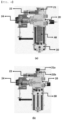
- FIG. 4(a) is a cross-sectional view illustrating an auxiliary chamber (20), a heating unit (30) and a bellows (40) before operating the heating unit
- FIG. 4(b) is a cross-sectional view illustrating the auxiliary chamber (20) and the heating unit (30) when operating the heating unit (30).
- the deposition apparatus (100) for an organic light emitting diode includes a main chamber (10) and a deposition source (A).
- the deposition source (A) includes an auxiliary chamber (20), a heating unit (30) and a bellows (40), and a deposition material is independently separated.
- the main chamber (10) is a constitution of depositing a deposition material on a substrate, and may include a substrate support on which a substrate is placed.
- the main chamber (10) is preferably provided having the inside to be in an atmosphere of vacuum state in order to deposit a deposition material on a substrate. Accordingly, the main chamber (10) may separately manage a vacuum atmosphere by a vacuum/atmospheric pressure control valve.
- the main chamber (10) may include a plurality of cells (not shown).
- the cell may be connected to a load unit (21) of the auxiliary chamber (20) and load a deposition material into the main chamber (10).
- the auxiliary chamber (20) is a constitution of being connected to the main chamber (10) and loading a deposition material to deposit. Accordingly, a container into which the deposition material is loaded may be included in the auxiliary chamber (20), and the auxiliary chamber (20) may be placed under the main chamber (10).
- the auxiliary chamber (20) may independently conduct maint in order to load the deposition material into the cell of the main chamber (10).
- the deposition apparatus (100) for an organic light emitting diode according to the present disclosure is capable of independently mainting one deposition material by the auxiliary chamber (20).
- the maint is a process for conducting a dummy process, and means venting a vacuum state of the auxiliary chamber (20), then placing an evaporation material, creating inside the auxiliary chamber (20) to be in a vacuum state again, and then conducting a dummy process.
- the dummy process means heating the auxiliary chamber (20) to remove impurities inside the auxiliary chamber (20), stabilize the degree of vacuum and vaporize a deposition material.
- the auxiliary chamber (20) may include a load unit (21, LTC) in order to load the deposition material into the cell of the main chamber (10).
- the load unit (21) is a constitution of connecting the auxiliary chamber (20) and the main chamber (10), and may be placed above the auxiliary chamber (20). In other words, the load unit (21) may bind to the cell of the main chamber (10) and load the deposition material into the main chamber (10).
- the load unit (21) may be provided in two levels.
- the second level (21a) of the two levels in the load unit (21) when a part inserted to the inside is the second level (21a) of the two levels in the load unit (21), only the first level (21b) may be provided in the load unit (21) when the main chamber (10) and the auxiliary chamber (20) are not connected.
- the load unit (21) may connect the main chamber (10) and the auxiliary chamber (20).
- the auxiliary chamber (20) may further include a gate valve (22) for controlling the deposition material moved through the load unit (21).
- the gate valve (22) may separate the atmosphere inside the auxiliary chamber (20) and the atmosphere inside the main chamber (10).
- the gate valve (22) may be placed in the middle of the load unit (21).
- the gate valve (22) is preferably closed before the load unit (21) is connected to the cell of the main chamber (10).
- the auxiliary chamber (20) may further include an opening/closing unit (23) on one side for loading and unloading the deposition material.
- the deposition material may enter and exit the auxiliary chamber (20) through the opening/closing unit (23), and the deposition material may be replaced in a container in the auxiliary chamber (20).
- the opening/closing unit (23) may further include a compression member (not shown) in order to maintain the atmosphere inside the auxiliary chamber.
- the compression member may be placed on a surface where the auxiliary chamber (20) and the opening/closing unit (23) are brought into contact with each other.
- the auxiliary chamber (20) may further include a vacuum unit (24) making the inside be in a vacuum state.
- the deposition apparatus (100) for an organic light emitting diode according to the present disclosure further includes a vacuum valve (25) between the auxiliary chamber (20) and the vacuum unit (24) to maintain the atmosphere inside the auxiliary chamber (20) and control the vacuum unit (24).
- the heating unit (30) is a constitution of heating the deposition material loaded into the auxiliary chamber (20).
- the heating unit (30) heats the auxiliary chamber (20) to a set temperature to stabilize the vacuum atmosphere inside the auxiliary chamber (20), and may vaporize the deposition material.
- the heating unit (30) may move up/down to effectively transfer generated heat to the auxiliary chamber (20) or to stop the dummy process.
- the deposition apparatus (100) for an organic light emitting diode may further include a bellows (40) connecting the auxiliary chamber (20) and the heating unit (30).
- the bellows (40) may move the heating unit (30) up/down through compression and tension. Heat generated in the heating unit (30) may be transferred to the auxiliary chamber (20) through the bellows (40).
- the second level of the load unit (21) may protrude to be connected to the cell of the main chamber (10) when the bellows (40) is compressed and the heating unit (30) moves toward the auxiliary chamber (20).
- the load unit (21) may protrude toward the main chamber (10) by the heat heated in the heating unit (30) and the pressure.
- the deposition apparatus (100) for an organic light emitting diode may further include a motor (not shown) in order to compress and decompress the bellows (40).
- the deposition apparatus (100) for an organic light emitting diode may include one or more of the auxiliary chamber (20) and the heating unit (30).
- the three different deposition materials may be each loaded into three auxiliary chambers (20) to conduct the maint.
- the auxiliary chamber (20) and the heating unit (30) are movable.
- the deposition apparatus (100) for an organic light emitting diode may further include, under the main chamber (10), a support unit capable of supporting the auxiliary chamber (20) and the heating unit (30), and a rail guiding the moving path, and the auxiliary chamber (20) and the heating unit (30) may move along the position of the cell of the main chamber (10).
Landscapes
- Chemical & Material Sciences (AREA)
- Engineering & Computer Science (AREA)
- Chemical Kinetics & Catalysis (AREA)
- Materials Engineering (AREA)
- Mechanical Engineering (AREA)
- Metallurgy (AREA)
- Organic Chemistry (AREA)
- Manufacturing & Machinery (AREA)
- Physical Vapour Deposition (AREA)
- Electroluminescent Light Sources (AREA)
Abstract
Description
- This application claims priority to and the benefits of
Korean Patent Application No. 10-2020-0154758, filed with the Korean Intellectual Property Office on November 18, 2020 - The present disclosure relates to a deposition apparatus for an organic light emitting diode, and in particular, to a deposition apparatus for an organic light emitting diode shortening a time of evaluation on a deposition material by independently mainting the deposition material through an auxiliary chamber.
- An organic light emitting diode (OLED) is an active light emitting device in which an organic film is provided between two electrodes separated upward and downward, and, when a current flows through the two electrodes, electrons and holes supplied from the two electrodes bind in the organic film to generate light. Such an OLED is thin and light and has properties of high luminance, low power consumption and the like, and is used in various fields. Particularly, an OLED has received attention as a next generation display, and may also be used as an illumination emitting white light and monochromatic light.
- In manufacturing an OLED, a process of forming an organic thin film and a process of forming a conductor thin film are required, and as such thin film forming processes, an evaporation deposition is mainly used.
- An organic thin film is mostly made in a manner such that a crucible holding a low molecular organic material is heated by flowing a current to a heating wire surrounding the crucible, the heat transferred to the crucible increases a temperature of the organic material in the crucible, and, as the temperature of the organic material increases, the organic material exits the crucible in a gas form and deposited on a substrate. In such manufacturing of organic thin film using a thermal deposition method, an OLED deposition device has been used.
-
FIG. 1 is a cross-sectional view illustrating an existing OLED deposition device. - When referring to
FIG. 1 , an existing OLED deposition device has a substrate (S) positioned on the upper portion, and on the lower portion, an OLED deposition device source for heating and evaporating a raw material to deposit the raw material on the substrate (S) and a thickness measurement sensor for measuring a thickness of the thin film deposited on the substrate are provided. - The OLED deposition device source is formed with a crucible accommodating an organic material, a raw material, therein, a heating means wound around the crucible to electrically heat the crucible, and a nozzle unit including a plurality of nozzles provided with a spray hole spraying the raw material evaporated from the crucible by the heating means.
- The existing OLED deposition device includes all deposition materials in one reaction chamber, and therefore, whenever an evaporation source is replaced, a vacuum state in the chamber is vented, a new evaporation material is placed, and inside the chamber is made to be in a vacuum state again to conduct a dummy process, which causes a problem in that the time of deposition and the time of evaluation take long.
- Accordingly, there have been needs for improving a deposition apparatus for an organic light emitting diode capable of evaluating some of all deposition materials or shortening a time of deposition.
- The present disclosure has been made in view of the above, and the present disclosure is directed to providing a deposition apparatus for an organic light emitting diode shortening a time of evaluation on a deposition material when partially depositing the deposition material by including a plurality of auxiliary chambers including the deposition material and capable of independently conducting maint.
- A deposition apparatus for an organic light emitting diode according to one embodiment of the present disclosure includes a main chamber depositing and evaluating a material; an auxiliary chamber connected to the main chamber and into which a deposition material to deposit is loaded; and a heating unit heating the deposition material loaded into the auxiliary chamber.
- In one embodiment, a bellows connecting the auxiliary chamber and the heating unit is included.
- In one embodiment, the auxiliary chamber includes a load unit loading the deposition material into a cell of the main chamber.
- In one embodiment, the load unit further includes a gate valve controlling movement of the deposition material.
- In one embodiment, a vacuum unit making inside the auxiliary chamber be in a vacuum state is further included.
- In one embodiment, the auxiliary chamber is placed under the main chamber.
- In one embodiment, the auxiliary chamber includes an opening/closing unit on one side for loading and unloading the deposition material.
- In one embodiment, the opening/closing unit further includes a compression member for maintaining an atmosphere inside the auxiliary chamber.
- In one embodiment, the auxiliary chamber and the heating unit are movable.
- In one embodiment, a motor compressing and decompressing the bellows is further included.
- According to the present disclosure, an effect of shortening a time of evaluation on a deposition material is obtained when partially depositing the deposition material by including a plurality of auxiliary chambers including the deposition material and capable of independently conducting maint.
-
-
FIG. 1 is a cross-sectional view illustrating an existing OLED deposition device. -
FIG. 2 is a perspective view illustrating a deposition apparatus for an organic light emitting diode according to one embodiment of the present disclosure. -
FIG. 3 is an enlarged perspective view of the part A ofFIG. 2 . -
FIG. 4(a) is a cross-sectional view illustrating an auxiliary chamber, a heating unit and a bellows before operating the heating unit, andFIG. 4(b) is a cross-sectional view illustrating the auxiliary chamber and the heating unit when operating the heating unit. -
- 100: Deposition Apparatus for Organic Light Emitting Diode
- 10: Main Chamber
- 20: Auxiliary Chamber
- 21: Load Unit
- 21a: Second Level of Load Unit
- 21b: First Level of Load Unit
- 22: Gate Valve
- 23: Opening/Closing Unit
- 24: Vacuum Unit
- 25: Vacuum Valve
- 30: Heating Unit
- 40: Bellows
- Detailed descriptions on the present disclosure are to fully describe the present disclosure to those skilled in the art. Throughout the specification, a description of a certain part "including" a certain constituent or being "characterized" by certain structure and shape does not exclude other constituents or exclude other structures and shapes and unless particularly stated on the contrary, and means capable of including other constituents, structures and shapes.
- The present disclosure may be diversely modified and may have various embodiments, and therefore, specific embodiments will be provided and described in detail in the detailed descriptions. However, this is not for limiting the contents of the present disclosure by the embodiments, and needs to be construed as including all modifications, equivalents and substitutes included in the ideas and the technical scope of the present disclosure.
-
FIG. 2 is a perspective view illustrating a deposition apparatus (100) for an organic light emitting diode according to one embodiment of the present disclosure,FIG. 3 is an enlarged perspective view of the part A ofFIG. 2 ,FIG. 4(a) is a cross-sectional view illustrating an auxiliary chamber (20), a heating unit (30) and a bellows (40) before operating the heating unit, andFIG. 4(b) is a cross-sectional view illustrating the auxiliary chamber (20) and the heating unit (30) when operating the heating unit (30). - The deposition apparatus (100) for an organic light emitting diode according to the present disclosure includes a main chamber (10) and a deposition source (A). Herein, the deposition source (A) includes an auxiliary chamber (20), a heating unit (30) and a bellows (40), and a deposition material is independently separated.
- The main chamber (10) is a constitution of depositing a deposition material on a substrate, and may include a substrate support on which a substrate is placed. The main chamber (10) is preferably provided having the inside to be in an atmosphere of vacuum state in order to deposit a deposition material on a substrate. Accordingly, the main chamber (10) may separately manage a vacuum atmosphere by a vacuum/atmospheric pressure control valve.
- The main chamber (10) may include a plurality of cells (not shown). The cell may be connected to a load unit (21) of the auxiliary chamber (20) and load a deposition material into the main chamber (10).
- The auxiliary chamber (20) is a constitution of being connected to the main chamber (10) and loading a deposition material to deposit. Accordingly, a container into which the deposition material is loaded may be included in the auxiliary chamber (20), and the auxiliary chamber (20) may be placed under the main chamber (10).
- The auxiliary chamber (20) may independently conduct maint in order to load the deposition material into the cell of the main chamber (10). In other words, the deposition apparatus (100) for an organic light emitting diode according to the present disclosure is capable of independently mainting one deposition material by the auxiliary chamber (20). Herein, the maint is a process for conducting a dummy process, and means venting a vacuum state of the auxiliary chamber (20), then placing an evaporation material, creating inside the auxiliary chamber (20) to be in a vacuum state again, and then conducting a dummy process. The dummy process means heating the auxiliary chamber (20) to remove impurities inside the auxiliary chamber (20), stabilize the degree of vacuum and vaporize a deposition material.
- Accordingly, the auxiliary chamber (20) may include a load unit (21, LTC) in order to load the deposition material into the cell of the main chamber (10). The load unit (21) is a constitution of connecting the auxiliary chamber (20) and the main chamber (10), and may be placed above the auxiliary chamber (20). In other words, the load unit (21) may bind to the cell of the main chamber (10) and load the deposition material into the main chamber (10).
- In one embodiment, the load unit (21) may be provided in two levels. Herein, when a part inserted to the inside is the second level (21a) of the two levels in the load unit (21), only the first level (21b) may be provided in the load unit (21) when the main chamber (10) and the auxiliary chamber (20) are not connected. By the second level (21a) protruding and being inserted to the cell of the main chamber (10) when conducting the dummy process, the load unit (21) may connect the main chamber (10) and the auxiliary chamber (20).
- The auxiliary chamber (20) may further include a gate valve (22) for controlling the deposition material moved through the load unit (21). In addition, the gate valve (22) may separate the atmosphere inside the auxiliary chamber (20) and the atmosphere inside the main chamber (10).
- The gate valve (22) may be placed in the middle of the load unit (21). The gate valve (22) is preferably closed before the load unit (21) is connected to the cell of the main chamber (10).
- The auxiliary chamber (20) may further include an opening/closing unit (23) on one side for loading and unloading the deposition material. In other words, the deposition material may enter and exit the auxiliary chamber (20) through the opening/closing unit (23), and the deposition material may be replaced in a container in the auxiliary chamber (20).
- In addition, the opening/closing unit (23) may further include a compression member (not shown) in order to maintain the atmosphere inside the auxiliary chamber. The compression member may be placed on a surface where the auxiliary chamber (20) and the opening/closing unit (23) are brought into contact with each other.
- After loading the deposition material into the container of the auxiliary chamber (20), the atmosphere formed inside the auxiliary chamber (20) needs to be the same as the atmosphere inside the main chamber (10). Accordingly, the auxiliary chamber (20) may further include a vacuum unit (24) making the inside be in a vacuum state. The deposition apparatus (100) for an organic light emitting diode according to the present disclosure further includes a vacuum valve (25) between the auxiliary chamber (20) and the vacuum unit (24) to maintain the atmosphere inside the auxiliary chamber (20) and control the vacuum unit (24).
- The heating unit (30) is a constitution of heating the deposition material loaded into the auxiliary chamber (20). The heating unit (30) heats the auxiliary chamber (20) to a set temperature to stabilize the vacuum atmosphere inside the auxiliary chamber (20), and may vaporize the deposition material.
- The heating unit (30) may move up/down to effectively transfer generated heat to the auxiliary chamber (20) or to stop the dummy process.
- Herein, the deposition apparatus (100) for an organic light emitting diode according to the present disclosure may further include a bellows (40) connecting the auxiliary chamber (20) and the heating unit (30). The bellows (40) may move the heating unit (30) up/down through compression and tension. Heat generated in the heating unit (30) may be transferred to the auxiliary chamber (20) through the bellows (40).
- In one embodiment, in the deposition apparatus (100) for an organic light emitting diode according to the present disclosure, the second level of the load unit (21) may protrude to be connected to the cell of the main chamber (10) when the bellows (40) is compressed and the heating unit (30) moves toward the auxiliary chamber (20). Herein, the load unit (21) may protrude toward the main chamber (10) by the heat heated in the heating unit (30) and the pressure.
- In addition, the deposition apparatus (100) for an organic light emitting diode according to the present disclosure may further include a motor (not shown) in order to compress and decompress the bellows (40).
- The deposition apparatus (100) for an organic light emitting diode according to the present disclosure may include one or more of the auxiliary chamber (20) and the heating unit (30). For example, when depositing three deposition materials, the three different deposition materials may be each loaded into three auxiliary chambers (20) to conduct the maint.
- In another embodiment, the auxiliary chamber (20) and the heating unit (30) are movable. Herein, the deposition apparatus (100) for an organic light emitting diode may further include, under the main chamber (10), a support unit capable of supporting the auxiliary chamber (20) and the heating unit (30), and a rail guiding the moving path, and the auxiliary chamber (20) and the heating unit (30) may move along the position of the cell of the main chamber (10).
- The present disclosure has been described with reference to preferred embodiments, however, those skilled in the art may understand that various modifications and changes may be made on the present disclosure within the scope not departing from the ideas and the territory of the present disclosure described in the appended claims.
Claims (10)
- A deposition apparatus for an organic light emitting diode, the deposition apparatus comprising:a main chamber depositing and evaluating a material;an auxiliary chamber connected to the main chamber and into which a deposition material to deposit is loaded; anda heating unit heating the deposition material loaded into the auxiliary chamber.
- The deposition apparatus for an organic light emitting diode of Claim 1, comprising a bellows connecting the auxiliary chamber and the heating unit.
- The deposition apparatus for an organic light emitting diode of Claim 1, wherein the auxiliary chamber includes a load unit loading the deposition material into a cell of the main chamber.
- The deposition apparatus for an organic light emitting diode of Claim 3, wherein the load unit further includes a gate valve controlling movement of the deposition material.
- The deposition apparatus for an organic light emitting diode of Claim 1, further comprising a vacuum unit making inside the auxiliary chamber to be in a vacuum state.
- The deposition apparatus for an organic light emitting diode of Claim 1, wherein the auxiliary chamber is placed under the main chamber.
- The deposition apparatus for an organic light emitting diode of Claim 1, wherein the auxiliary chamber includes an opening/closing unit on one side for loading and unloading the deposition material.
- The deposition apparatus for an organic light emitting diode of Claim 7, wherein the opening/closing unit further includes a compression member for maintaining an atmosphere inside the auxiliary chamber.
- The deposition apparatus for an organic light emitting diode of Claim 1, wherein the auxiliary chamber and the heating unit are movable.
- The deposition apparatus for an organic light emitting diode of Claim 2, further comprising a motor compressing and decompressing the bellows.
Applications Claiming Priority (2)
| Application Number | Priority Date | Filing Date | Title |
|---|---|---|---|
| KR1020200154758A KR102859881B1 (en) | 2020-11-18 | 2020-11-18 | Deposition equipment of organic light emitting diodes |
| PCT/KR2021/016862 WO2022108326A1 (en) | 2020-11-18 | 2021-11-17 | Deposition apparatus for organic light-emitting diode |
Publications (2)
| Publication Number | Publication Date |
|---|---|
| EP4190937A1 true EP4190937A1 (en) | 2023-06-07 |
| EP4190937A4 EP4190937A4 (en) | 2023-12-27 |
Family
ID=81709358
Family Applications (1)
| Application Number | Title | Priority Date | Filing Date |
|---|---|---|---|
| EP21895094.7A Pending EP4190937A4 (en) | 2020-11-18 | 2021-11-17 | DEPOSITION DEVICE FOR ORGANIC LIGHT-LIGHT DIODE |
Country Status (7)
| Country | Link |
|---|---|
| US (1) | US20230329076A1 (en) |
| EP (1) | EP4190937A4 (en) |
| JP (1) | JP7732631B2 (en) |
| KR (1) | KR102859881B1 (en) |
| CN (1) | CN115968413B (en) |
| TW (1) | TWI792687B (en) |
| WO (1) | WO2022108326A1 (en) |
Family Cites Families (19)
| Publication number | Priority date | Publication date | Assignee | Title |
|---|---|---|---|---|
| US5356673A (en) * | 1991-03-18 | 1994-10-18 | Jet Process Corporation | Evaporation system and method for gas jet deposition of thin film materials |
| JP3452617B2 (en) * | 1993-12-10 | 2003-09-29 | 真空冶金株式会社 | Gas deposition equipment |
| JP4436664B2 (en) * | 2003-12-24 | 2010-03-24 | 日立造船株式会社 | Vapor deposition equipment |
| JP4570403B2 (en) * | 2004-06-28 | 2010-10-27 | 日立造船株式会社 | Evaporation apparatus, vapor deposition apparatus, and method for switching evaporation apparatus in vapor deposition apparatus |
| KR100958778B1 (en) * | 2004-10-22 | 2010-05-18 | 황창훈 | Evaporation source continuous feeder for organic thin film deposition process |
| US20090087339A1 (en) * | 2007-09-28 | 2009-04-02 | Asm Japan K.K. | METHOD FOR FORMING RUTHENIUM COMPLEX FILM USING Beta-DIKETONE-COORDINATED RUTHENIUM PRECURSOR |
| EP2168643A1 (en) * | 2008-09-29 | 2010-03-31 | Applied Materials, Inc. | Evaporator for organic materials |
| JP2010159448A (en) * | 2009-01-07 | 2010-07-22 | Canon Inc | Film deposition apparatus and film deposition method |
| WO2011074551A1 (en) * | 2009-12-18 | 2011-06-23 | 平田機工株式会社 | Vacuum deposition method and vacuum deposition apparatus |
| TWI564427B (en) * | 2009-12-18 | 2017-01-01 | 財團法人工業技術研究院 | Method for forming parylene film |
| KR102137181B1 (en) * | 2013-12-06 | 2020-08-13 | 어플라이드 머티어리얼스, 인코포레이티드 | Depositing arrangement, deposition apparatus and methods of operation thereof |
| JP2016181468A (en) * | 2015-03-25 | 2016-10-13 | 株式会社ジャパンディスプレイ | Manufacturing method for organic el display device, and film thickness measurement device |
| US9932666B2 (en) * | 2015-03-30 | 2018-04-03 | Siva Power, Inc. | Fluid-assisted thermal management of evaporation sources |
| KR20160133589A (en) | 2015-05-12 | 2016-11-23 | 주식회사 파인에바 | Linear Evaporation Deposition Apparatus |
| CN105441878B (en) * | 2016-01-05 | 2018-12-21 | 京东方科技集团股份有限公司 | Heating device and evaporated device for vapor deposition |
| KR102107288B1 (en) * | 2017-01-02 | 2020-05-06 | 황창훈 | Framed large size plane type evaporation source apparatus |
| DE102017003516A1 (en) * | 2017-04-11 | 2018-10-11 | Creaphys Gmbh | Coating apparatus and method for reactive vapor deposition under vacuum on a substrate |
| WO2019142812A1 (en) * | 2018-01-19 | 2019-07-25 | 株式会社アルバック | Heater base and processing device |
| KR102310236B1 (en) * | 2018-10-23 | 2021-10-08 | 어플라이드 머티어리얼스, 인코포레이티드 | Evaporation Source For Automatic Exchange Of Crucible And Evaporation Deposition System Having The Same |
-
2020
- 2020-11-18 KR KR1020200154758A patent/KR102859881B1/en active Active
-
2021
- 2021-11-17 CN CN202180051514.8A patent/CN115968413B/en active Active
- 2021-11-17 TW TW110142802A patent/TWI792687B/en active
- 2021-11-17 EP EP21895094.7A patent/EP4190937A4/en active Pending
- 2021-11-17 JP JP2023512308A patent/JP7732631B2/en active Active
- 2021-11-17 US US18/023,590 patent/US20230329076A1/en active Pending
- 2021-11-17 WO PCT/KR2021/016862 patent/WO2022108326A1/en not_active Ceased
Also Published As
| Publication number | Publication date |
|---|---|
| CN115968413B (en) | 2026-04-24 |
| TWI792687B (en) | 2023-02-11 |
| TW202230853A (en) | 2022-08-01 |
| CN115968413A (en) | 2023-04-14 |
| KR20220067947A (en) | 2022-05-25 |
| EP4190937A4 (en) | 2023-12-27 |
| US20230329076A1 (en) | 2023-10-12 |
| JP7732631B2 (en) | 2025-09-02 |
| WO2022108326A1 (en) | 2022-05-27 |
| KR102859881B1 (en) | 2025-09-12 |
| JP2023538735A (en) | 2023-09-11 |
Similar Documents
| Publication | Publication Date | Title |
|---|---|---|
| JP5358778B2 (en) | Film forming apparatus, evaporation jig, and measuring method | |
| US8383194B2 (en) | Film forming apparatus, film forming system, film forming method, and method of manufacturing electronic device or organic electroluminescence element | |
| US8679369B2 (en) | Film-forming material and method for predicting film-forming material | |
| KR20100114905A (en) | Film forming source, deposition apparatus and apparatus for manufacturing organic el element | |
| US20230329076A1 (en) | Deposition apparatus for organic light-emitting diode | |
| CN109321884A (en) | Evaporation coating device | |
| KR20100002078A (en) | Deposition source, film forming apparatus and film forming method | |
| JP2017073397A (en) | Reduced pressure dryer, reduced pressure drying method, and baking-treatment system | |
| KR20110020878A (en) | Substrate Coating Equipment | |
| KR100627679B1 (en) | Large Area Substrate Arrangement | |
| EP1512768A1 (en) | Method for forming organic thin film | |
| KR20060031966A (en) | Organic material deposition equipment and substrate loading method of organic material deposition equipment | |
| KR20040103726A (en) | Large size organic electro luminescence evaporation source application | |
| KR20150060038A (en) | Organic deposition device | |
| JP4949644B2 (en) | Method for manufacturing Josephson element | |
| KR100887227B1 (en) | Thin film deposition apparatus | |
| KR100695271B1 (en) | Pattern formation method of large area OLD board | |
| KR20190143660A (en) | Evaporation source for deposition device | |
| KR20190134156A (en) | OLED Deposition Source having Multi Hole Structure | |
| KR20210143659A (en) | Evaporation source apparatus, vapor deposition apparatus and control method of evaporation source apparatus | |
| KR20200040384A (en) | Evaporation source and deposition device | |
| JP2010144212A (en) | Material supply apparatus and material supply method | |
| KR20070030087A (en) | Vacuum deposition equipment for ODL |
Legal Events
| Date | Code | Title | Description |
|---|---|---|---|
| STAA | Information on the status of an ep patent application or granted ep patent |
Free format text: STATUS: THE INTERNATIONAL PUBLICATION HAS BEEN MADE |
|
| PUAI | Public reference made under article 153(3) epc to a published international application that has entered the european phase |
Free format text: ORIGINAL CODE: 0009012 |
|
| STAA | Information on the status of an ep patent application or granted ep patent |
Free format text: STATUS: REQUEST FOR EXAMINATION WAS MADE |
|
| 17P | Request for examination filed |
Effective date: 20230303 |
|
| AK | Designated contracting states |
Kind code of ref document: A1 Designated state(s): AL AT BE BG CH CY CZ DE DK EE ES FI FR GB GR HR HU IE IS IT LI LT LU LV MC MK MT NL NO PL PT RO RS SE SI SK SM TR |
|
| A4 | Supplementary search report drawn up and despatched |
Effective date: 20231127 |
|
| RIC1 | Information provided on ipc code assigned before grant |
Ipc: C23C 14/26 20060101ALI20231121BHEP Ipc: B01B 1/00 20060101ALI20231121BHEP Ipc: C23C 14/12 20060101ALI20231121BHEP Ipc: C23C 14/54 20060101ALI20231121BHEP Ipc: C23C 14/24 20060101AFI20231121BHEP |
|
| DAV | Request for validation of the european patent (deleted) | ||
| DAX | Request for extension of the european patent (deleted) |