EP4188053A1 - Photoelectric conversion element, photoelectric conversion module, electronic device, and partition - Google Patents
Photoelectric conversion element, photoelectric conversion module, electronic device, and partition Download PDFInfo
- Publication number
- EP4188053A1 EP4188053A1 EP22207497.3A EP22207497A EP4188053A1 EP 4188053 A1 EP4188053 A1 EP 4188053A1 EP 22207497 A EP22207497 A EP 22207497A EP 4188053 A1 EP4188053 A1 EP 4188053A1
- Authority
- EP
- European Patent Office
- Prior art keywords
- photoelectric conversion
- conversion element
- electrode
- examples
- group
- Prior art date
- Legal status (The legal status is an assumption and is not a legal conclusion. Google has not performed a legal analysis and makes no representation as to the accuracy of the status listed.)
- Pending
Links
- 238000006243 chemical reaction Methods 0.000 title claims abstract description 492
- 238000005192 partition Methods 0.000 title claims description 73
- 238000007789 sealing Methods 0.000 claims abstract description 133
- 239000000758 substrate Substances 0.000 claims abstract description 107
- 239000002070 nanowire Substances 0.000 claims abstract description 35
- 229920001940 conductive polymer Polymers 0.000 claims abstract description 29
- 239000002274 desiccant Substances 0.000 claims abstract description 26
- -1 pyridine compound Chemical class 0.000 claims description 142
- 239000000463 material Substances 0.000 claims description 98
- 230000005525 hole transport Effects 0.000 claims description 95
- 239000004065 semiconductor Substances 0.000 claims description 55
- 238000002834 transmittance Methods 0.000 claims description 42
- 230000005611 electricity Effects 0.000 claims description 37
- BQCADISMDOOEFD-UHFFFAOYSA-N Silver Chemical compound [Ag] BQCADISMDOOEFD-UHFFFAOYSA-N 0.000 claims description 31
- 239000004820 Pressure-sensitive adhesive Substances 0.000 claims description 27
- 229910003002 lithium salt Inorganic materials 0.000 claims description 27
- 159000000002 lithium salts Chemical class 0.000 claims description 27
- 230000004224 protection Effects 0.000 claims description 20
- XLYOFNOQVPJJNP-UHFFFAOYSA-N water Chemical compound O XLYOFNOQVPJJNP-UHFFFAOYSA-N 0.000 claims description 20
- 239000002042 Silver nanowire Substances 0.000 claims description 19
- 210000000352 storage cell Anatomy 0.000 claims description 13
- 150000007514 bases Chemical class 0.000 claims description 10
- JUJWROOIHBZHMG-UHFFFAOYSA-N pyridine Substances C1=CC=NC=C1 JUJWROOIHBZHMG-UHFFFAOYSA-N 0.000 claims description 10
- UMJSCPRVCHMLSP-UHFFFAOYSA-N pyridine Natural products COC1=CC=CN=C1 UMJSCPRVCHMLSP-UHFFFAOYSA-N 0.000 claims description 10
- 239000010410 layer Substances 0.000 description 267
- 238000000034 method Methods 0.000 description 164
- 150000001875 compounds Chemical class 0.000 description 140
- 230000032258 transport Effects 0.000 description 85
- 208000017983 photosensitivity disease Diseases 0.000 description 66
- 231100000434 photosensitization Toxicity 0.000 description 66
- 125000001424 substituent group Chemical group 0.000 description 63
- 210000004027 cell Anatomy 0.000 description 57
- 125000000217 alkyl group Chemical group 0.000 description 56
- 239000002904 solvent Substances 0.000 description 42
- 239000010408 film Substances 0.000 description 40
- 229920005989 resin Polymers 0.000 description 35
- 239000011347 resin Substances 0.000 description 35
- 239000000047 product Substances 0.000 description 33
- 229910052751 metal Inorganic materials 0.000 description 31
- 239000002184 metal Substances 0.000 description 30
- 239000007788 liquid Substances 0.000 description 29
- 229910052760 oxygen Inorganic materials 0.000 description 29
- QVGXLLKOCUKJST-UHFFFAOYSA-N atomic oxygen Chemical compound [O] QVGXLLKOCUKJST-UHFFFAOYSA-N 0.000 description 28
- 125000004432 carbon atom Chemical group C* 0.000 description 28
- 238000000576 coating method Methods 0.000 description 28
- 239000001301 oxygen Substances 0.000 description 28
- 125000001997 phenyl group Chemical group [H]C1=C([H])C([H])=C(*)C([H])=C1[H] 0.000 description 27
- 230000015572 biosynthetic process Effects 0.000 description 25
- 230000000903 blocking effect Effects 0.000 description 25
- 239000003795 chemical substances by application Substances 0.000 description 25
- 239000011521 glass Substances 0.000 description 23
- 238000007639 printing Methods 0.000 description 22
- 238000010248 power generation Methods 0.000 description 21
- 239000011248 coating agent Substances 0.000 description 19
- 125000003118 aryl group Chemical group 0.000 description 18
- LFQSCWFLJHTTHZ-UHFFFAOYSA-N Ethanol Chemical compound CCO LFQSCWFLJHTTHZ-UHFFFAOYSA-N 0.000 description 17
- 150000004700 cobalt complex Chemical class 0.000 description 17
- 239000012530 fluid Substances 0.000 description 17
- 150000002500 ions Chemical class 0.000 description 17
- 239000000243 solution Substances 0.000 description 17
- 238000003860 storage Methods 0.000 description 17
- 239000000975 dye Substances 0.000 description 16
- 230000000694 effects Effects 0.000 description 16
- 239000003822 epoxy resin Substances 0.000 description 16
- 229920000647 polyepoxide Polymers 0.000 description 16
- UHOVQNZJYSORNB-UHFFFAOYSA-N Benzene Chemical compound C1=CC=CC=C1 UHOVQNZJYSORNB-UHFFFAOYSA-N 0.000 description 15
- YMWUJEATGCHHMB-UHFFFAOYSA-N Dichloromethane Chemical compound ClCCl YMWUJEATGCHHMB-UHFFFAOYSA-N 0.000 description 15
- OKKJLVBELUTLKV-UHFFFAOYSA-N Methanol Chemical compound OC OKKJLVBELUTLKV-UHFFFAOYSA-N 0.000 description 15
- YXFVVABEGXRONW-UHFFFAOYSA-N Toluene Chemical compound CC1=CC=CC=C1 YXFVVABEGXRONW-UHFFFAOYSA-N 0.000 description 15
- RTZKZFJDLAIYFH-UHFFFAOYSA-N Diethyl ether Chemical compound CCOCC RTZKZFJDLAIYFH-UHFFFAOYSA-N 0.000 description 14
- 230000003247 decreasing effect Effects 0.000 description 14
- 229910052744 lithium Inorganic materials 0.000 description 14
- 239000002245 particle Substances 0.000 description 14
- 238000012545 processing Methods 0.000 description 13
- 230000009257 reactivity Effects 0.000 description 13
- CSCPPACGZOOCGX-UHFFFAOYSA-N Acetone Chemical compound CC(C)=O CSCPPACGZOOCGX-UHFFFAOYSA-N 0.000 description 12
- OKTJSMMVPCPJKN-UHFFFAOYSA-N Carbon Chemical compound [C] OKTJSMMVPCPJKN-UHFFFAOYSA-N 0.000 description 12
- CURLTUGMZLYLDI-UHFFFAOYSA-N Carbon dioxide Chemical compound O=C=O CURLTUGMZLYLDI-UHFFFAOYSA-N 0.000 description 12
- XEKOWRVHYACXOJ-UHFFFAOYSA-N Ethyl acetate Chemical compound CCOC(C)=O XEKOWRVHYACXOJ-UHFFFAOYSA-N 0.000 description 12
- XEEYBQQBJWHFJM-UHFFFAOYSA-N Iron Chemical compound [Fe] XEEYBQQBJWHFJM-UHFFFAOYSA-N 0.000 description 12
- WHXSMMKQMYFTQS-UHFFFAOYSA-N Lithium Chemical compound [Li] WHXSMMKQMYFTQS-UHFFFAOYSA-N 0.000 description 12
- ZMXDDKWLCZADIW-UHFFFAOYSA-N N,N-Dimethylformamide Chemical compound CN(C)C=O ZMXDDKWLCZADIW-UHFFFAOYSA-N 0.000 description 12
- MVPPADPHJFYWMZ-UHFFFAOYSA-N chlorobenzene Chemical compound ClC1=CC=CC=C1 MVPPADPHJFYWMZ-UHFFFAOYSA-N 0.000 description 12
- 230000001965 increasing effect Effects 0.000 description 12
- 229910052757 nitrogen Inorganic materials 0.000 description 12
- 229910052709 silver Inorganic materials 0.000 description 12
- 239000004332 silver Substances 0.000 description 12
- 239000013078 crystal Substances 0.000 description 11
- 239000006185 dispersion Substances 0.000 description 11
- 238000009413 insulation Methods 0.000 description 11
- 238000012423 maintenance Methods 0.000 description 11
- 229910044991 metal oxide Inorganic materials 0.000 description 11
- 150000004706 metal oxides Chemical class 0.000 description 11
- 239000011368 organic material Substances 0.000 description 11
- 239000003960 organic solvent Substances 0.000 description 11
- 229920000123 polythiophene Polymers 0.000 description 11
- 239000003566 sealing material Substances 0.000 description 11
- 239000000126 substance Substances 0.000 description 11
- HEDRZPFGACZZDS-UHFFFAOYSA-N Chloroform Chemical compound ClC(Cl)Cl HEDRZPFGACZZDS-UHFFFAOYSA-N 0.000 description 10
- GWEVSGVZZGPLCZ-UHFFFAOYSA-N Titan oxide Chemical compound O=[Ti]=O GWEVSGVZZGPLCZ-UHFFFAOYSA-N 0.000 description 10
- XLOMVQKBTHCTTD-UHFFFAOYSA-N Zinc monoxide Chemical compound [Zn]=O XLOMVQKBTHCTTD-UHFFFAOYSA-N 0.000 description 10
- 125000003545 alkoxy group Chemical group 0.000 description 10
- 150000001450 anions Chemical class 0.000 description 10
- 230000005540 biological transmission Effects 0.000 description 10
- 238000010586 diagram Methods 0.000 description 10
- 239000000945 filler Substances 0.000 description 10
- LNEPOXFFQSENCJ-UHFFFAOYSA-N haloperidol Chemical compound C1CC(O)(C=2C=CC(Cl)=CC=2)CCN1CCCC(=O)C1=CC=C(F)C=C1 LNEPOXFFQSENCJ-UHFFFAOYSA-N 0.000 description 10
- 150000002430 hydrocarbons Chemical class 0.000 description 10
- 125000004435 hydrogen atom Chemical group [H]* 0.000 description 10
- 239000007800 oxidant agent Substances 0.000 description 10
- 230000035515 penetration Effects 0.000 description 10
- 238000011282 treatment Methods 0.000 description 10
- 229910001868 water Inorganic materials 0.000 description 10
- ZWEHNKRNPOVVGH-UHFFFAOYSA-N 2-Butanone Chemical compound CCC(C)=O ZWEHNKRNPOVVGH-UHFFFAOYSA-N 0.000 description 9
- 239000004215 Carbon black (E152) Substances 0.000 description 9
- KFZMGEQAYNKOFK-UHFFFAOYSA-N Isopropanol Chemical compound CC(C)O KFZMGEQAYNKOFK-UHFFFAOYSA-N 0.000 description 9
- VYPSYNLAJGMNEJ-UHFFFAOYSA-N Silicium dioxide Chemical compound O=[Si]=O VYPSYNLAJGMNEJ-UHFFFAOYSA-N 0.000 description 9
- 239000002253 acid Substances 0.000 description 9
- 125000003277 amino group Chemical group 0.000 description 9
- 238000010304 firing Methods 0.000 description 9
- 229930195733 hydrocarbon Natural products 0.000 description 9
- 239000002861 polymer material Substances 0.000 description 9
- 239000002356 single layer Substances 0.000 description 9
- 238000004528 spin coating Methods 0.000 description 9
- 239000007921 spray Substances 0.000 description 9
- RFFLAFLAYFXFSW-UHFFFAOYSA-N 1,2-dichlorobenzene Chemical compound ClC1=CC=CC=C1Cl RFFLAFLAYFXFSW-UHFFFAOYSA-N 0.000 description 8
- IJGRMHOSHXDMSA-UHFFFAOYSA-N Atomic nitrogen Chemical compound N#N IJGRMHOSHXDMSA-UHFFFAOYSA-N 0.000 description 8
- XMWRBQBLMFGWIX-UHFFFAOYSA-N C60 fullerene Chemical compound C12=C3C(C4=C56)=C7C8=C5C5=C9C%10=C6C6=C4C1=C1C4=C6C6=C%10C%10=C9C9=C%11C5=C8C5=C8C7=C3C3=C7C2=C1C1=C2C4=C6C4=C%10C6=C9C9=C%11C5=C5C8=C3C3=C7C1=C1C2=C4C6=C2C9=C5C3=C12 XMWRBQBLMFGWIX-UHFFFAOYSA-N 0.000 description 8
- PXHVJJICTQNCMI-UHFFFAOYSA-N Nickel Chemical compound [Ni] PXHVJJICTQNCMI-UHFFFAOYSA-N 0.000 description 8
- WYURNTSHIVDZCO-UHFFFAOYSA-N Tetrahydrofuran Chemical compound C1CCOC1 WYURNTSHIVDZCO-UHFFFAOYSA-N 0.000 description 8
- YTPLMLYBLZKORZ-UHFFFAOYSA-N Thiophene Chemical group C=1C=CSC=1 YTPLMLYBLZKORZ-UHFFFAOYSA-N 0.000 description 8
- 238000010521 absorption reaction Methods 0.000 description 8
- 125000004453 alkoxycarbonyl group Chemical group 0.000 description 8
- 229910052793 cadmium Inorganic materials 0.000 description 8
- BDOSMKKIYDKNTQ-UHFFFAOYSA-N cadmium atom Chemical compound [Cd] BDOSMKKIYDKNTQ-UHFFFAOYSA-N 0.000 description 8
- 229910052799 carbon Inorganic materials 0.000 description 8
- 150000001768 cations Chemical class 0.000 description 8
- 239000003086 colorant Substances 0.000 description 8
- 230000000052 comparative effect Effects 0.000 description 8
- 230000007423 decrease Effects 0.000 description 8
- 150000003949 imides Chemical class 0.000 description 8
- 239000010409 thin film Substances 0.000 description 8
- XOLBLPGZBRYERU-UHFFFAOYSA-N tin dioxide Chemical compound O=[Sn]=O XOLBLPGZBRYERU-UHFFFAOYSA-N 0.000 description 8
- 229910001887 tin oxide Inorganic materials 0.000 description 8
- OGIDPMRJRNCKJF-UHFFFAOYSA-N titanium oxide Inorganic materials [Ti]=O OGIDPMRJRNCKJF-UHFFFAOYSA-N 0.000 description 8
- 239000011701 zinc Substances 0.000 description 8
- 108700032487 GAP-43-3 Proteins 0.000 description 7
- LRHPLDYGYMQRHN-UHFFFAOYSA-N N-Butanol Chemical compound CCCCO LRHPLDYGYMQRHN-UHFFFAOYSA-N 0.000 description 7
- SECXISVLQFMRJM-UHFFFAOYSA-N N-Methylpyrrolidone Chemical compound CN1CCCC1=O SECXISVLQFMRJM-UHFFFAOYSA-N 0.000 description 7
- CTQNGGLPUBDAKN-UHFFFAOYSA-N O-Xylene Chemical group CC1=CC=CC=C1C CTQNGGLPUBDAKN-UHFFFAOYSA-N 0.000 description 7
- 229910002092 carbon dioxide Inorganic materials 0.000 description 7
- 229920001971 elastomer Polymers 0.000 description 7
- 239000007789 gas Substances 0.000 description 7
- 229910052736 halogen Inorganic materials 0.000 description 7
- 238000004519 manufacturing process Methods 0.000 description 7
- 238000000691 measurement method Methods 0.000 description 7
- 239000000203 mixture Substances 0.000 description 7
- 125000001624 naphthyl group Chemical group 0.000 description 7
- 239000005060 rubber Substances 0.000 description 7
- 238000007650 screen-printing Methods 0.000 description 7
- WEVYAHXRMPXWCK-UHFFFAOYSA-N Acetonitrile Chemical compound CC#N WEVYAHXRMPXWCK-UHFFFAOYSA-N 0.000 description 6
- YNQLUTRBYVCPMQ-UHFFFAOYSA-N Ethylbenzene Chemical compound CCC1=CC=CC=C1 YNQLUTRBYVCPMQ-UHFFFAOYSA-N 0.000 description 6
- URLKBWYHVLBVBO-UHFFFAOYSA-N Para-Xylene Chemical group CC1=CC=C(C)C=C1 URLKBWYHVLBVBO-UHFFFAOYSA-N 0.000 description 6
- OFBQJSOFQDEBGM-UHFFFAOYSA-N Pentane Chemical compound CCCCC OFBQJSOFQDEBGM-UHFFFAOYSA-N 0.000 description 6
- 239000004721 Polyphenylene oxide Substances 0.000 description 6
- DKGAVHZHDRPRBM-UHFFFAOYSA-N Tert-Butanol Chemical compound CC(C)(C)O DKGAVHZHDRPRBM-UHFFFAOYSA-N 0.000 description 6
- 238000000833 X-ray absorption fine structure spectroscopy Methods 0.000 description 6
- HCHKCACWOHOZIP-UHFFFAOYSA-N Zinc Chemical compound [Zn] HCHKCACWOHOZIP-UHFFFAOYSA-N 0.000 description 6
- 150000001408 amides Chemical class 0.000 description 6
- QARVLSVVCXYDNA-UHFFFAOYSA-N bromobenzene Chemical compound BrC1=CC=CC=C1 QARVLSVVCXYDNA-UHFFFAOYSA-N 0.000 description 6
- DIKBFYAXUHHXCS-UHFFFAOYSA-N bromoform Chemical compound BrC(Br)Br DIKBFYAXUHHXCS-UHFFFAOYSA-N 0.000 description 6
- DKPFZGUDAPQIHT-UHFFFAOYSA-N butyl acetate Chemical compound CCCCOC(C)=O DKPFZGUDAPQIHT-UHFFFAOYSA-N 0.000 description 6
- RWGFKTVRMDUZSP-UHFFFAOYSA-N cumene Chemical compound CC(C)C1=CC=CC=C1 RWGFKTVRMDUZSP-UHFFFAOYSA-N 0.000 description 6
- MGNZXYYWBUKAII-UHFFFAOYSA-N cyclohexa-1,3-diene Chemical compound C1CC=CC=C1 MGNZXYYWBUKAII-UHFFFAOYSA-N 0.000 description 6
- 238000007607 die coating method Methods 0.000 description 6
- 238000010494 dissociation reaction Methods 0.000 description 6
- 230000005593 dissociations Effects 0.000 description 6
- 150000002222 fluorine compounds Chemical class 0.000 description 6
- 230000006870 function Effects 0.000 description 6
- 150000008282 halocarbons Chemical class 0.000 description 6
- 238000010438 heat treatment Methods 0.000 description 6
- 230000006872 improvement Effects 0.000 description 6
- 229910052738 indium Inorganic materials 0.000 description 6
- APFVFJFRJDLVQX-UHFFFAOYSA-N indium atom Chemical compound [In] APFVFJFRJDLVQX-UHFFFAOYSA-N 0.000 description 6
- 125000003387 indolinyl group Chemical class N1(CCC2=CC=CC=C12)* 0.000 description 6
- 238000009434 installation Methods 0.000 description 6
- IVSZLXZYQVIEFR-UHFFFAOYSA-N m-xylene Chemical group CC1=CC=CC(C)=C1 IVSZLXZYQVIEFR-UHFFFAOYSA-N 0.000 description 6
- 229910001507 metal halide Inorganic materials 0.000 description 6
- 150000005309 metal halides Chemical class 0.000 description 6
- UAEPNZWRGJTJPN-UHFFFAOYSA-N methylcyclohexane Chemical compound CC1CCCCC1 UAEPNZWRGJTJPN-UHFFFAOYSA-N 0.000 description 6
- VLKZOEOYAKHREP-UHFFFAOYSA-N n-Hexane Chemical compound CCCCCC VLKZOEOYAKHREP-UHFFFAOYSA-N 0.000 description 6
- TVMXDCGIABBOFY-UHFFFAOYSA-N octane Chemical compound CCCCCCCC TVMXDCGIABBOFY-UHFFFAOYSA-N 0.000 description 6
- BASFCYQUMIYNBI-UHFFFAOYSA-N platinum Chemical compound [Pt] BASFCYQUMIYNBI-UHFFFAOYSA-N 0.000 description 6
- 229920003217 poly(methylsilsesquioxane) Polymers 0.000 description 6
- 229920000570 polyether Polymers 0.000 description 6
- 238000001228 spectrum Methods 0.000 description 6
- 238000004544 sputter deposition Methods 0.000 description 6
- 150000003577 thiophenes Chemical class 0.000 description 6
- 229910052725 zinc Inorganic materials 0.000 description 6
- JTPNRXUCIXHOKM-UHFFFAOYSA-N 1-chloronaphthalene Chemical compound C1=CC=C2C(Cl)=CC=CC2=C1 JTPNRXUCIXHOKM-UHFFFAOYSA-N 0.000 description 5
- QTBSBXVTEAMEQO-UHFFFAOYSA-N Acetic acid Chemical compound CC(O)=O QTBSBXVTEAMEQO-UHFFFAOYSA-N 0.000 description 5
- RYGMFSIKBFXOCR-UHFFFAOYSA-N Copper Chemical compound [Cu] RYGMFSIKBFXOCR-UHFFFAOYSA-N 0.000 description 5
- XUIMIQQOPSSXEZ-UHFFFAOYSA-N Silicon Chemical compound [Si] XUIMIQQOPSSXEZ-UHFFFAOYSA-N 0.000 description 5
- 230000002776 aggregation Effects 0.000 description 5
- 238000004220 aggregation Methods 0.000 description 5
- 229910052783 alkali metal Inorganic materials 0.000 description 5
- 125000003342 alkenyl group Chemical group 0.000 description 5
- 125000000304 alkynyl group Chemical group 0.000 description 5
- 230000004888 barrier function Effects 0.000 description 5
- 239000001569 carbon dioxide Substances 0.000 description 5
- 238000009833 condensation Methods 0.000 description 5
- 230000005494 condensation Effects 0.000 description 5
- 229920001577 copolymer Polymers 0.000 description 5
- 229910052802 copper Inorganic materials 0.000 description 5
- 239000010949 copper Substances 0.000 description 5
- 125000000332 coumarinyl group Chemical class O1C(=O)C(=CC2=CC=CC=C12)* 0.000 description 5
- 238000011156 evaluation Methods 0.000 description 5
- 238000007756 gravure coating Methods 0.000 description 5
- 125000000623 heterocyclic group Chemical group 0.000 description 5
- 229910052742 iron Inorganic materials 0.000 description 5
- ZIRAMZRKLHPLPK-UHFFFAOYSA-N lithium fluorosulfonyl(trifluoromethylsulfonyl)azanide Chemical compound FS(=O)(=O)[N-]S(=O)(=O)C(F)(F)F.[Li+] ZIRAMZRKLHPLPK-UHFFFAOYSA-N 0.000 description 5
- 238000007645 offset printing Methods 0.000 description 5
- IEQIEDJGQAUEQZ-UHFFFAOYSA-N phthalocyanine Chemical class N1C(N=C2C3=CC=CC=C3C(N=C3C4=CC=CC=C4C(=N4)N3)=N2)=C(C=CC=C2)C2=C1N=C1C2=CC=CC=C2C4=N1 IEQIEDJGQAUEQZ-UHFFFAOYSA-N 0.000 description 5
- 239000002985 plastic film Substances 0.000 description 5
- 229920000642 polymer Polymers 0.000 description 5
- 230000009467 reduction Effects 0.000 description 5
- 238000007761 roller coating Methods 0.000 description 5
- 239000010703 silicon Substances 0.000 description 5
- 229910052710 silicon Inorganic materials 0.000 description 5
- YLQBMQCUIZJEEH-UHFFFAOYSA-N tetrahydrofuran Natural products C=1C=COC=1 YLQBMQCUIZJEEH-UHFFFAOYSA-N 0.000 description 5
- 239000011787 zinc oxide Substances 0.000 description 5
- QGKMIGUHVLGJBR-UHFFFAOYSA-M (4z)-1-(3-methylbutyl)-4-[[1-(3-methylbutyl)quinolin-1-ium-4-yl]methylidene]quinoline;iodide Chemical compound [I-].C12=CC=CC=C2N(CCC(C)C)C=CC1=CC1=CC=[N+](CCC(C)C)C2=CC=CC=C12 QGKMIGUHVLGJBR-UHFFFAOYSA-M 0.000 description 4
- SCYULBFZEHDVBN-UHFFFAOYSA-N 1,1-Dichloroethane Chemical compound CC(Cl)Cl SCYULBFZEHDVBN-UHFFFAOYSA-N 0.000 description 4
- 239000004925 Acrylic resin Substances 0.000 description 4
- 229920000178 Acrylic resin Polymers 0.000 description 4
- BAVYZALUXZFZLV-UHFFFAOYSA-N Methylamine Chemical compound NC BAVYZALUXZFZLV-UHFFFAOYSA-N 0.000 description 4
- KDLHZDBZIXYQEI-UHFFFAOYSA-N Palladium Chemical compound [Pd] KDLHZDBZIXYQEI-UHFFFAOYSA-N 0.000 description 4
- ATJFFYVFTNAWJD-UHFFFAOYSA-N Tin Chemical compound [Sn] ATJFFYVFTNAWJD-UHFFFAOYSA-N 0.000 description 4
- RTAQQCXQSZGOHL-UHFFFAOYSA-N Titanium Chemical compound [Ti] RTAQQCXQSZGOHL-UHFFFAOYSA-N 0.000 description 4
- 239000000654 additive Substances 0.000 description 4
- 239000000853 adhesive Substances 0.000 description 4
- 230000001070 adhesive effect Effects 0.000 description 4
- 239000000443 aerosol Substances 0.000 description 4
- 150000003973 alkyl amines Chemical class 0.000 description 4
- 238000004458 analytical method Methods 0.000 description 4
- 238000000137 annealing Methods 0.000 description 4
- 125000003710 aryl alkyl group Chemical group 0.000 description 4
- ODINCKMPIJJUCX-UHFFFAOYSA-N calcium oxide Inorganic materials [Ca]=O ODINCKMPIJJUCX-UHFFFAOYSA-N 0.000 description 4
- 150000001868 cobalt Chemical class 0.000 description 4
- 238000007796 conventional method Methods 0.000 description 4
- 238000001514 detection method Methods 0.000 description 4
- 238000001035 drying Methods 0.000 description 4
- 239000004210 ether based solvent Substances 0.000 description 4
- 230000001747 exhibiting effect Effects 0.000 description 4
- PCHJSUWPFVWCPO-UHFFFAOYSA-N gold Chemical compound [Au] PCHJSUWPFVWCPO-UHFFFAOYSA-N 0.000 description 4
- 229910052737 gold Inorganic materials 0.000 description 4
- 239000010931 gold Substances 0.000 description 4
- 238000007646 gravure printing Methods 0.000 description 4
- 150000002367 halogens Chemical group 0.000 description 4
- WABPQHHGFIMREM-UHFFFAOYSA-N lead(0) Chemical compound [Pb] WABPQHHGFIMREM-UHFFFAOYSA-N 0.000 description 4
- HSZCZNFXUDYRKD-UHFFFAOYSA-M lithium iodide Chemical compound [Li+].[I-] HSZCZNFXUDYRKD-UHFFFAOYSA-M 0.000 description 4
- CPLXHLVBOLITMK-UHFFFAOYSA-N magnesium oxide Inorganic materials [Mg]=O CPLXHLVBOLITMK-UHFFFAOYSA-N 0.000 description 4
- DZVCFNFOPIZQKX-LTHRDKTGSA-M merocyanine Chemical compound [Na+].O=C1N(CCCC)C(=O)N(CCCC)C(=O)C1=C\C=C\C=C/1N(CCCS([O-])(=O)=O)C2=CC=CC=C2O\1 DZVCFNFOPIZQKX-LTHRDKTGSA-M 0.000 description 4
- 229910052759 nickel Inorganic materials 0.000 description 4
- 125000004430 oxygen atom Chemical group O* 0.000 description 4
- 230000002688 persistence Effects 0.000 description 4
- 229920000553 poly(phenylenevinylene) Polymers 0.000 description 4
- 229920000767 polyaniline Polymers 0.000 description 4
- 229920000128 polypyrrole Polymers 0.000 description 4
- 239000000843 powder Substances 0.000 description 4
- 238000003672 processing method Methods 0.000 description 4
- 150000003222 pyridines Chemical class 0.000 description 4
- 238000000926 separation method Methods 0.000 description 4
- 150000003384 small molecules Chemical class 0.000 description 4
- 238000003980 solgel method Methods 0.000 description 4
- 229910052717 sulfur Inorganic materials 0.000 description 4
- 229910052718 tin Inorganic materials 0.000 description 4
- 125000001889 triflyl group Chemical group FC(F)(F)S(*)(=O)=O 0.000 description 4
- 238000001771 vacuum deposition Methods 0.000 description 4
- NAWXUBYGYWOOIX-SFHVURJKSA-N (2s)-2-[[4-[2-(2,4-diaminoquinazolin-6-yl)ethyl]benzoyl]amino]-4-methylidenepentanedioic acid Chemical compound C1=CC2=NC(N)=NC(N)=C2C=C1CCC1=CC=C(C(=O)N[C@@H](CC(=C)C(O)=O)C(O)=O)C=C1 NAWXUBYGYWOOIX-SFHVURJKSA-N 0.000 description 3
- UOCLXMDMGBRAIB-UHFFFAOYSA-N 1,1,1-trichloroethane Chemical compound CC(Cl)(Cl)Cl UOCLXMDMGBRAIB-UHFFFAOYSA-N 0.000 description 3
- WNXJIVFYUVYPPR-UHFFFAOYSA-N 1,3-dioxolane Chemical compound C1COCO1 WNXJIVFYUVYPPR-UHFFFAOYSA-N 0.000 description 3
- RYHBNJHYFVUHQT-UHFFFAOYSA-N 1,4-Dioxane Chemical compound C1COCCO1 RYHBNJHYFVUHQT-UHFFFAOYSA-N 0.000 description 3
- PRBHEGAFLDMLAL-UHFFFAOYSA-N 1,5-Hexadiene Natural products CC=CCC=C PRBHEGAFLDMLAL-UHFFFAOYSA-N 0.000 description 3
- UJOBWOGCFQCDNV-UHFFFAOYSA-N 9H-carbazole Chemical compound C1=CC=C2C3=CC=CC=C3NC2=C1 UJOBWOGCFQCDNV-UHFFFAOYSA-N 0.000 description 3
- XDTMQSROBMDMFD-UHFFFAOYSA-N Cyclohexane Chemical compound C1CCCCC1 XDTMQSROBMDMFD-UHFFFAOYSA-N 0.000 description 3
- XTHFKEDIFFGKHM-UHFFFAOYSA-N Dimethoxyethane Chemical compound COCCOC XTHFKEDIFFGKHM-UHFFFAOYSA-N 0.000 description 3
- LYCAIKOWRPUZTN-UHFFFAOYSA-N Ethylene glycol Chemical compound OCCO LYCAIKOWRPUZTN-UHFFFAOYSA-N 0.000 description 3
- UUIQMZJEGPQKFD-UHFFFAOYSA-N Methyl butyrate Chemical compound CCCC(=O)OC UUIQMZJEGPQKFD-UHFFFAOYSA-N 0.000 description 3
- NTIZESTWPVYFNL-UHFFFAOYSA-N Methyl isobutyl ketone Chemical compound CC(C)CC(C)=O NTIZESTWPVYFNL-UHFFFAOYSA-N 0.000 description 3
- UIHCLUNTQKBZGK-UHFFFAOYSA-N Methyl isobutyl ketone Natural products CCC(C)C(C)=O UIHCLUNTQKBZGK-UHFFFAOYSA-N 0.000 description 3
- FXHOOIRPVKKKFG-UHFFFAOYSA-N N,N-Dimethylacetamide Chemical compound CN(C)C(C)=O FXHOOIRPVKKKFG-UHFFFAOYSA-N 0.000 description 3
- 229920000265 Polyparaphenylene Chemical class 0.000 description 3
- XBDQKXXYIPTUBI-UHFFFAOYSA-M Propionate Chemical compound CCC([O-])=O XBDQKXXYIPTUBI-UHFFFAOYSA-M 0.000 description 3
- BLRPTPMANUNPDV-UHFFFAOYSA-N Silane Chemical group [SiH4] BLRPTPMANUNPDV-UHFFFAOYSA-N 0.000 description 3
- XSTXAVWGXDQKEL-UHFFFAOYSA-N Trichloroethylene Chemical group ClC=C(Cl)Cl XSTXAVWGXDQKEL-UHFFFAOYSA-N 0.000 description 3
- 238000004998 X ray absorption near edge structure spectroscopy Methods 0.000 description 3
- 229910021536 Zeolite Inorganic materials 0.000 description 3
- 230000000996 additive effect Effects 0.000 description 3
- 239000005456 alcohol based solvent Substances 0.000 description 3
- XAGFODPZIPBFFR-UHFFFAOYSA-N aluminium Chemical compound [Al] XAGFODPZIPBFFR-UHFFFAOYSA-N 0.000 description 3
- 229910052787 antimony Inorganic materials 0.000 description 3
- WATWJIUSRGPENY-UHFFFAOYSA-N antimony atom Chemical compound [Sb] WATWJIUSRGPENY-UHFFFAOYSA-N 0.000 description 3
- YCOXTKKNXUZSKD-UHFFFAOYSA-N as-o-xylenol Natural products CC1=CC=C(O)C=C1C YCOXTKKNXUZSKD-UHFFFAOYSA-N 0.000 description 3
- 229910052797 bismuth Inorganic materials 0.000 description 3
- JCXGWMGPZLAOME-UHFFFAOYSA-N bismuth atom Chemical compound [Bi] JCXGWMGPZLAOME-UHFFFAOYSA-N 0.000 description 3
- 229950005228 bromoform Drugs 0.000 description 3
- BTANRVKWQNVYAZ-UHFFFAOYSA-N butan-2-ol Chemical compound CCC(C)O BTANRVKWQNVYAZ-UHFFFAOYSA-N 0.000 description 3
- 239000000292 calcium oxide Substances 0.000 description 3
- 150000004770 chalcogenides Chemical class 0.000 description 3
- 239000011651 chromium Substances 0.000 description 3
- 229910017052 cobalt Inorganic materials 0.000 description 3
- 239000010941 cobalt Substances 0.000 description 3
- GUTLYIVDDKVIGB-UHFFFAOYSA-N cobalt atom Chemical compound [Co] GUTLYIVDDKVIGB-UHFFFAOYSA-N 0.000 description 3
- 239000007822 coupling agent Substances 0.000 description 3
- 238000000151 deposition Methods 0.000 description 3
- RAABOESOVLLHRU-UHFFFAOYSA-N diazene Chemical compound N=N RAABOESOVLLHRU-UHFFFAOYSA-N 0.000 description 3
- 229910000071 diazene Inorganic materials 0.000 description 3
- HNPSIPDUKPIQMN-UHFFFAOYSA-N dioxosilane;oxo(oxoalumanyloxy)alumane Chemical compound O=[Si]=O.O=[Al]O[Al]=O HNPSIPDUKPIQMN-UHFFFAOYSA-N 0.000 description 3
- 238000005401 electroluminescence Methods 0.000 description 3
- 239000003759 ester based solvent Substances 0.000 description 3
- 238000005530 etching Methods 0.000 description 3
- JBTWLSYIZRCDFO-UHFFFAOYSA-N ethyl methyl carbonate Chemical compound CCOC(=O)OC JBTWLSYIZRCDFO-UHFFFAOYSA-N 0.000 description 3
- 238000000605 extraction Methods 0.000 description 3
- WBJINCZRORDGAQ-UHFFFAOYSA-N formic acid ethyl ester Natural products CCOC=O WBJINCZRORDGAQ-UHFFFAOYSA-N 0.000 description 3
- 229910003472 fullerene Inorganic materials 0.000 description 3
- PYGSKMBEVAICCR-UHFFFAOYSA-N hexa-1,5-diene Chemical compound C=CCCC=C PYGSKMBEVAICCR-UHFFFAOYSA-N 0.000 description 3
- 150000002497 iodine compounds Chemical class 0.000 description 3
- SNHMUERNLJLMHN-UHFFFAOYSA-N iodobenzene Chemical compound IC1=CC=CC=C1 SNHMUERNLJLMHN-UHFFFAOYSA-N 0.000 description 3
- INQOMBQAUSQDDS-UHFFFAOYSA-N iodomethane Chemical compound IC INQOMBQAUSQDDS-UHFFFAOYSA-N 0.000 description 3
- 239000005453 ketone based solvent Substances 0.000 description 3
- 150000002576 ketones Chemical class 0.000 description 3
- 230000031700 light absorption Effects 0.000 description 3
- QSZMZKBZAYQGRS-UHFFFAOYSA-N lithium;bis(trifluoromethylsulfonyl)azanide Chemical compound [Li+].FC(F)(F)S(=O)(=O)[N-]S(=O)(=O)C(F)(F)F QSZMZKBZAYQGRS-UHFFFAOYSA-N 0.000 description 3
- 239000000395 magnesium oxide Substances 0.000 description 3
- 235000012245 magnesium oxide Nutrition 0.000 description 3
- 150000002739 metals Chemical class 0.000 description 3
- GYNNXHKOJHMOHS-UHFFFAOYSA-N methyl-cycloheptane Natural products CC1CCCCCC1 GYNNXHKOJHMOHS-UHFFFAOYSA-N 0.000 description 3
- PYLWMHQQBFSUBP-UHFFFAOYSA-N monofluorobenzene Chemical compound FC1=CC=CC=C1 PYLWMHQQBFSUBP-UHFFFAOYSA-N 0.000 description 3
- 229940078552 o-xylene Drugs 0.000 description 3
- 150000002892 organic cations Chemical group 0.000 description 3
- 150000002894 organic compounds Chemical class 0.000 description 3
- 238000002161 passivation Methods 0.000 description 3
- 229920006255 plastic film Polymers 0.000 description 3
- 229910052697 platinum Inorganic materials 0.000 description 3
- 229920002098 polyfluorene Chemical class 0.000 description 3
- 150000004032 porphyrins Chemical class 0.000 description 3
- NLKNQRATVPKPDG-UHFFFAOYSA-M potassium iodide Chemical compound [K+].[I-] NLKNQRATVPKPDG-UHFFFAOYSA-M 0.000 description 3
- BDERNNFJNOPAEC-UHFFFAOYSA-N propan-1-ol Chemical compound CCCO BDERNNFJNOPAEC-UHFFFAOYSA-N 0.000 description 3
- 239000011435 rock Substances 0.000 description 3
- FVAUCKIRQBBSSJ-UHFFFAOYSA-M sodium iodide Chemical compound [Na+].[I-] FVAUCKIRQBBSSJ-UHFFFAOYSA-M 0.000 description 3
- 238000001179 sorption measurement Methods 0.000 description 3
- 238000003756 stirring Methods 0.000 description 3
- 125000004434 sulfur atom Chemical group 0.000 description 3
- 239000004094 surface-active agent Substances 0.000 description 3
- 229910052715 tantalum Inorganic materials 0.000 description 3
- GUVRBAGPIYLISA-UHFFFAOYSA-N tantalum atom Chemical compound [Ta] GUVRBAGPIYLISA-UHFFFAOYSA-N 0.000 description 3
- DHCDFWKWKRSZHF-UHFFFAOYSA-L thiosulfate(2-) Chemical compound [O-]S([S-])(=O)=O DHCDFWKWKRSZHF-UHFFFAOYSA-L 0.000 description 3
- 239000011135 tin Substances 0.000 description 3
- 229910052719 titanium Inorganic materials 0.000 description 3
- 239000010936 titanium Substances 0.000 description 3
- UBOXGVDOUJQMTN-UHFFFAOYSA-N trichloroethylene Natural products ClCC(Cl)Cl UBOXGVDOUJQMTN-UHFFFAOYSA-N 0.000 description 3
- WFKWXMTUELFFGS-UHFFFAOYSA-N tungsten Chemical compound [W] WFKWXMTUELFFGS-UHFFFAOYSA-N 0.000 description 3
- 229910052721 tungsten Inorganic materials 0.000 description 3
- 239000010937 tungsten Substances 0.000 description 3
- 238000007740 vapor deposition Methods 0.000 description 3
- 239000010457 zeolite Substances 0.000 description 3
- YBYIRNPNPLQARY-UHFFFAOYSA-N 1H-indene Chemical compound C1=CC=C2CC=CC2=C1 YBYIRNPNPLQARY-UHFFFAOYSA-N 0.000 description 2
- ZFFMLCVRJBZUDZ-UHFFFAOYSA-N 2,3-dimethylbutane Chemical compound CC(C)C(C)C ZFFMLCVRJBZUDZ-UHFFFAOYSA-N 0.000 description 2
- HZAXFHJVJLSVMW-UHFFFAOYSA-N 2-Aminoethan-1-ol Chemical compound NCCO HZAXFHJVJLSVMW-UHFFFAOYSA-N 0.000 description 2
- YEJRWHAVMIAJKC-UHFFFAOYSA-N 4-Butyrolactone Chemical compound O=C1CCCO1 YEJRWHAVMIAJKC-UHFFFAOYSA-N 0.000 description 2
- 239000005964 Acibenzolar-S-methyl Substances 0.000 description 2
- QGZKDVFQNNGYKY-UHFFFAOYSA-N Ammonia Chemical compound N QGZKDVFQNNGYKY-UHFFFAOYSA-N 0.000 description 2
- XKRFYHLGVUSROY-UHFFFAOYSA-N Argon Chemical compound [Ar] XKRFYHLGVUSROY-UHFFFAOYSA-N 0.000 description 2
- JBRZTFJDHDCESZ-UHFFFAOYSA-N AsGa Chemical compound [As]#[Ga] JBRZTFJDHDCESZ-UHFFFAOYSA-N 0.000 description 2
- BVKZGUZCCUSVTD-UHFFFAOYSA-M Bicarbonate Chemical compound OC([O-])=O BVKZGUZCCUSVTD-UHFFFAOYSA-M 0.000 description 2
- VTYYLEPIZMXCLO-UHFFFAOYSA-L Calcium carbonate Chemical compound [Ca+2].[O-]C([O-])=O VTYYLEPIZMXCLO-UHFFFAOYSA-L 0.000 description 2
- UXVMQQNJUSDDNG-UHFFFAOYSA-L Calcium chloride Chemical compound [Cl-].[Cl-].[Ca+2] UXVMQQNJUSDDNG-UHFFFAOYSA-L 0.000 description 2
- 229910052684 Cerium Inorganic materials 0.000 description 2
- LCGLNKUTAGEVQW-UHFFFAOYSA-N Dimethyl ether Chemical compound COC LCGLNKUTAGEVQW-UHFFFAOYSA-N 0.000 description 2
- IAZDPXIOMUYVGZ-UHFFFAOYSA-N Dimethylsulphoxide Chemical compound CS(C)=O IAZDPXIOMUYVGZ-UHFFFAOYSA-N 0.000 description 2
- QUSNBJAOOMFDIB-UHFFFAOYSA-N Ethylamine Chemical compound CCN QUSNBJAOOMFDIB-UHFFFAOYSA-N 0.000 description 2
- GYHNNYVSQQEPJS-UHFFFAOYSA-N Gallium Chemical compound [Ga] GYHNNYVSQQEPJS-UHFFFAOYSA-N 0.000 description 2
- 229910001218 Gallium arsenide Inorganic materials 0.000 description 2
- 206010019345 Heat stroke Diseases 0.000 description 2
- VEXZGXHMUGYJMC-UHFFFAOYSA-N Hydrochloric acid Chemical compound Cl VEXZGXHMUGYJMC-UHFFFAOYSA-N 0.000 description 2
- 238000004566 IR spectroscopy Methods 0.000 description 2
- CSNNHWWHGAXBCP-UHFFFAOYSA-L Magnesium sulfate Chemical compound [Mg+2].[O-][S+2]([O-])([O-])[O-] CSNNHWWHGAXBCP-UHFFFAOYSA-L 0.000 description 2
- 229910019142 PO4 Inorganic materials 0.000 description 2
- WCUXLLCKKVVCTQ-UHFFFAOYSA-M Potassium chloride Chemical compound [Cl-].[K+] WCUXLLCKKVVCTQ-UHFFFAOYSA-M 0.000 description 2
- ATUOYWHBWRKTHZ-UHFFFAOYSA-N Propane Chemical compound CCC ATUOYWHBWRKTHZ-UHFFFAOYSA-N 0.000 description 2
- KJTLSVCANCCWHF-UHFFFAOYSA-N Ruthenium Chemical compound [Ru] KJTLSVCANCCWHF-UHFFFAOYSA-N 0.000 description 2
- 229910052581 Si3N4 Inorganic materials 0.000 description 2
- 239000006087 Silane Coupling Agent Substances 0.000 description 2
- FAPWRFPIFSIZLT-UHFFFAOYSA-M Sodium chloride Chemical compound [Na+].[Cl-] FAPWRFPIFSIZLT-UHFFFAOYSA-M 0.000 description 2
- PPBRXRYQALVLMV-UHFFFAOYSA-N Styrene Chemical compound C=CC1=CC=CC=C1 PPBRXRYQALVLMV-UHFFFAOYSA-N 0.000 description 2
- 230000006750 UV protection Effects 0.000 description 2
- QCWXUUIWCKQGHC-UHFFFAOYSA-N Zirconium Chemical compound [Zr] QCWXUUIWCKQGHC-UHFFFAOYSA-N 0.000 description 2
- KTSFMFGEAAANTF-UHFFFAOYSA-N [Cu].[Se].[Se].[In] Chemical compound [Cu].[Se].[Se].[In] KTSFMFGEAAANTF-UHFFFAOYSA-N 0.000 description 2
- 239000011358 absorbing material Substances 0.000 description 2
- YRKCREAYFQTBPV-UHFFFAOYSA-N acetylacetone Chemical compound CC(=O)CC(C)=O YRKCREAYFQTBPV-UHFFFAOYSA-N 0.000 description 2
- 150000008065 acid anhydrides Chemical class 0.000 description 2
- 125000002252 acyl group Chemical group 0.000 description 2
- 239000012790 adhesive layer Substances 0.000 description 2
- 150000001298 alcohols Chemical class 0.000 description 2
- 125000001931 aliphatic group Chemical group 0.000 description 2
- 150000001336 alkenes Chemical class 0.000 description 2
- 125000004414 alkyl thio group Chemical group 0.000 description 2
- 229910052782 aluminium Inorganic materials 0.000 description 2
- PNEYBMLMFCGWSK-UHFFFAOYSA-N aluminium oxide Inorganic materials [O-2].[O-2].[O-2].[Al+3].[Al+3] PNEYBMLMFCGWSK-UHFFFAOYSA-N 0.000 description 2
- 150000001412 amines Chemical class 0.000 description 2
- 125000005428 anthryl group Chemical group [H]C1=C([H])C([H])=C2C([H])=C3C(*)=C([H])C([H])=C([H])C3=C([H])C2=C1[H] 0.000 description 2
- 239000003963 antioxidant agent Substances 0.000 description 2
- 239000007864 aqueous solution Substances 0.000 description 2
- 238000000231 atomic layer deposition Methods 0.000 description 2
- QVQLCTNNEUAWMS-UHFFFAOYSA-N barium oxide Chemical compound [Ba]=O QVQLCTNNEUAWMS-UHFFFAOYSA-N 0.000 description 2
- JRPBQTZRNDNNOP-UHFFFAOYSA-N barium titanate Chemical compound [Ba+2].[Ba+2].[O-][Ti]([O-])([O-])[O-] JRPBQTZRNDNNOP-UHFFFAOYSA-N 0.000 description 2
- 229910002113 barium titanate Inorganic materials 0.000 description 2
- 230000008901 benefit Effects 0.000 description 2
- WMWLMWRWZQELOS-UHFFFAOYSA-N bismuth(iii) oxide Chemical compound O=[Bi]O[Bi]=O WMWLMWRWZQELOS-UHFFFAOYSA-N 0.000 description 2
- IISBACLAFKSPIT-UHFFFAOYSA-N bisphenol A Chemical compound C=1C=C(O)C=CC=1C(C)(C)C1=CC=C(O)C=C1 IISBACLAFKSPIT-UHFFFAOYSA-N 0.000 description 2
- PXKLMJQFEQBVLD-UHFFFAOYSA-N bisphenol F Chemical compound C1=CC(O)=CC=C1CC1=CC=C(O)C=C1 PXKLMJQFEQBVLD-UHFFFAOYSA-N 0.000 description 2
- 238000005422 blasting Methods 0.000 description 2
- 229910052792 caesium Inorganic materials 0.000 description 2
- 239000001110 calcium chloride Substances 0.000 description 2
- 229910001628 calcium chloride Inorganic materials 0.000 description 2
- 235000011148 calcium chloride Nutrition 0.000 description 2
- BRPQOXSCLDDYGP-UHFFFAOYSA-N calcium oxide Chemical compound [O-2].[Ca+2] BRPQOXSCLDDYGP-UHFFFAOYSA-N 0.000 description 2
- AOWKSNWVBZGMTJ-UHFFFAOYSA-N calcium titanate Chemical compound [Ca+2].[O-][Ti]([O-])=O AOWKSNWVBZGMTJ-UHFFFAOYSA-N 0.000 description 2
- 125000003917 carbamoyl group Chemical group [H]N([H])C(*)=O 0.000 description 2
- 150000001721 carbon Chemical group 0.000 description 2
- 239000002041 carbon nanotube Substances 0.000 description 2
- 229910021393 carbon nanotube Inorganic materials 0.000 description 2
- 125000002915 carbonyl group Chemical group [*:2]C([*:1])=O 0.000 description 2
- 239000000969 carrier Substances 0.000 description 2
- 239000000919 ceramic Substances 0.000 description 2
- ZMIGMASIKSOYAM-UHFFFAOYSA-N cerium Chemical compound [Ce][Ce][Ce][Ce][Ce][Ce][Ce][Ce][Ce][Ce][Ce][Ce][Ce][Ce][Ce][Ce][Ce][Ce][Ce][Ce][Ce][Ce][Ce][Ce][Ce][Ce][Ce][Ce][Ce][Ce][Ce][Ce][Ce][Ce][Ce][Ce][Ce][Ce] ZMIGMASIKSOYAM-UHFFFAOYSA-N 0.000 description 2
- 230000008859 change Effects 0.000 description 2
- 239000002738 chelating agent Substances 0.000 description 2
- 238000003486 chemical etching Methods 0.000 description 2
- 238000005229 chemical vapour deposition Methods 0.000 description 2
- 239000000460 chlorine Substances 0.000 description 2
- 229940125898 compound 5 Drugs 0.000 description 2
- 229920000547 conjugated polymer Polymers 0.000 description 2
- 239000000470 constituent Substances 0.000 description 2
- 150000004696 coordination complex Chemical group 0.000 description 2
- LCUOIYYHNRBAFS-UHFFFAOYSA-N copper;sulfanylideneindium Chemical compound [Cu].[In]=S LCUOIYYHNRBAFS-UHFFFAOYSA-N 0.000 description 2
- 125000004093 cyano group Chemical group *C#N 0.000 description 2
- 230000008021 deposition Effects 0.000 description 2
- 230000006866 deterioration Effects 0.000 description 2
- 238000009792 diffusion process Methods 0.000 description 2
- WHGNXNCOTZPEEK-UHFFFAOYSA-N dimethoxy-methyl-[3-(oxiran-2-ylmethoxy)propyl]silane Chemical compound CO[Si](C)(OC)CCCOCC1CO1 WHGNXNCOTZPEEK-UHFFFAOYSA-N 0.000 description 2
- 239000002612 dispersion medium Substances 0.000 description 2
- GNTDGMZSJNCJKK-UHFFFAOYSA-N divanadium pentaoxide Chemical compound O=[V](=O)O[V](=O)=O GNTDGMZSJNCJKK-UHFFFAOYSA-N 0.000 description 2
- 239000007772 electrode material Substances 0.000 description 2
- 230000007613 environmental effect Effects 0.000 description 2
- 125000001495 ethyl group Chemical group [H]C([H])([H])C([H])([H])* 0.000 description 2
- 239000000835 fiber Substances 0.000 description 2
- 229910052733 gallium Inorganic materials 0.000 description 2
- 239000000499 gel Substances 0.000 description 2
- 229910052732 germanium Inorganic materials 0.000 description 2
- GNPVGFCGXDBREM-UHFFFAOYSA-N germanium atom Chemical compound [Ge] GNPVGFCGXDBREM-UHFFFAOYSA-N 0.000 description 2
- 229910052735 hafnium Inorganic materials 0.000 description 2
- VBJZVLUMGGDVMO-UHFFFAOYSA-N hafnium atom Chemical compound [Hf] VBJZVLUMGGDVMO-UHFFFAOYSA-N 0.000 description 2
- 150000002460 imidazoles Chemical class 0.000 description 2
- 238000007654 immersion Methods 0.000 description 2
- 229910052741 iridium Inorganic materials 0.000 description 2
- GKOZUEZYRPOHIO-UHFFFAOYSA-N iridium atom Chemical compound [Ir] GKOZUEZYRPOHIO-UHFFFAOYSA-N 0.000 description 2
- ZXEKIIBDNHEJCQ-UHFFFAOYSA-N isobutanol Chemical compound CC(C)CO ZXEKIIBDNHEJCQ-UHFFFAOYSA-N 0.000 description 2
- 229910052746 lanthanum Inorganic materials 0.000 description 2
- FZLIPJUXYLNCLC-UHFFFAOYSA-N lanthanum atom Chemical compound [La] FZLIPJUXYLNCLC-UHFFFAOYSA-N 0.000 description 2
- 239000011133 lead Substances 0.000 description 2
- 239000003446 ligand Substances 0.000 description 2
- 229910003473 lithium bis(trifluoromethanesulfonyl)imide Inorganic materials 0.000 description 2
- AMXOYNBUYSYVKV-UHFFFAOYSA-M lithium bromide Chemical compound [Li+].[Br-] AMXOYNBUYSYVKV-UHFFFAOYSA-M 0.000 description 2
- KWGKDLIKAYFUFQ-UHFFFAOYSA-M lithium chloride Chemical compound [Li+].[Cl-] KWGKDLIKAYFUFQ-UHFFFAOYSA-M 0.000 description 2
- 150000002642 lithium compounds Chemical class 0.000 description 2
- MHCFAGZWMAWTNR-UHFFFAOYSA-M lithium perchlorate Chemical compound [Li+].[O-]Cl(=O)(=O)=O MHCFAGZWMAWTNR-UHFFFAOYSA-M 0.000 description 2
- 229910001486 lithium perchlorate Inorganic materials 0.000 description 2
- ACFSQHQYDZIPRL-UHFFFAOYSA-N lithium;bis(1,1,2,2,2-pentafluoroethylsulfonyl)azanide Chemical compound [Li+].FC(F)(F)C(F)(F)S(=O)(=O)[N-]S(=O)(=O)C(F)(F)C(F)(F)F ACFSQHQYDZIPRL-UHFFFAOYSA-N 0.000 description 2
- VDVLPSWVDYJFRW-UHFFFAOYSA-N lithium;bis(fluorosulfonyl)azanide Chemical compound [Li+].FS(=O)(=O)[N-]S(F)(=O)=O VDVLPSWVDYJFRW-UHFFFAOYSA-N 0.000 description 2
- AXZKOIWUVFPNLO-UHFFFAOYSA-N magnesium;oxygen(2-) Chemical compound [O-2].[Mg+2] AXZKOIWUVFPNLO-UHFFFAOYSA-N 0.000 description 2
- 238000005259 measurement Methods 0.000 description 2
- 230000008018 melting Effects 0.000 description 2
- 238000002844 melting Methods 0.000 description 2
- 125000002496 methyl group Chemical group [H]C([H])([H])* 0.000 description 2
- 229910000476 molybdenum oxide Inorganic materials 0.000 description 2
- 238000000465 moulding Methods 0.000 description 2
- 125000001280 n-hexyl group Chemical group C(CCCCC)* 0.000 description 2
- 229910052758 niobium Inorganic materials 0.000 description 2
- 239000010955 niobium Substances 0.000 description 2
- GUCVJGMIXFAOAE-UHFFFAOYSA-N niobium atom Chemical compound [Nb] GUCVJGMIXFAOAE-UHFFFAOYSA-N 0.000 description 2
- 229910000484 niobium oxide Inorganic materials 0.000 description 2
- URLJKFSTXLNXLG-UHFFFAOYSA-N niobium(5+);oxygen(2-) Chemical compound [O-2].[O-2].[O-2].[O-2].[O-2].[Nb+5].[Nb+5] URLJKFSTXLNXLG-UHFFFAOYSA-N 0.000 description 2
- 229910017604 nitric acid Inorganic materials 0.000 description 2
- 229910000510 noble metal Inorganic materials 0.000 description 2
- 125000005151 nonafluorobutanesulfonyl group Chemical group FC(C(C(S(=O)(=O)*)(F)F)(F)F)(C(F)(F)F)F 0.000 description 2
- QGLKJKCYBOYXKC-UHFFFAOYSA-N nonaoxidotritungsten Chemical compound O=[W]1(=O)O[W](=O)(=O)O[W](=O)(=O)O1 QGLKJKCYBOYXKC-UHFFFAOYSA-N 0.000 description 2
- JRZJOMJEPLMPRA-UHFFFAOYSA-N olefin Natural products CCCCCCCC=C JRZJOMJEPLMPRA-UHFFFAOYSA-N 0.000 description 2
- 239000005416 organic matter Substances 0.000 description 2
- 229910052762 osmium Inorganic materials 0.000 description 2
- SYQBFIAQOQZEGI-UHFFFAOYSA-N osmium atom Chemical compound [Os] SYQBFIAQOQZEGI-UHFFFAOYSA-N 0.000 description 2
- 150000004866 oxadiazoles Chemical class 0.000 description 2
- TWNQGVIAIRXVLR-UHFFFAOYSA-N oxo(oxoalumanyloxy)alumane Chemical compound O=[Al]O[Al]=O TWNQGVIAIRXVLR-UHFFFAOYSA-N 0.000 description 2
- PQQKPALAQIIWST-UHFFFAOYSA-N oxomolybdenum Chemical compound [Mo]=O PQQKPALAQIIWST-UHFFFAOYSA-N 0.000 description 2
- 229910052763 palladium Inorganic materials 0.000 description 2
- 230000000149 penetrating effect Effects 0.000 description 2
- VLTRZXGMWDSKGL-UHFFFAOYSA-N perchloric acid Substances OCl(=O)(=O)=O VLTRZXGMWDSKGL-UHFFFAOYSA-N 0.000 description 2
- 239000012466 permeate Substances 0.000 description 2
- 125000005561 phenanthryl group Chemical group 0.000 description 2
- 229920003023 plastic Polymers 0.000 description 2
- 238000007747 plating Methods 0.000 description 2
- 229920000768 polyamine Polymers 0.000 description 2
- IOLCXVTUBQKXJR-UHFFFAOYSA-M potassium bromide Chemical compound [K+].[Br-] IOLCXVTUBQKXJR-UHFFFAOYSA-M 0.000 description 2
- UKDIAJWKFXFVFG-UHFFFAOYSA-N potassium;oxido(dioxo)niobium Chemical compound [K+].[O-][Nb](=O)=O UKDIAJWKFXFVFG-UHFFFAOYSA-N 0.000 description 2
- 238000001556 precipitation Methods 0.000 description 2
- 238000003825 pressing Methods 0.000 description 2
- 239000011164 primary particle Substances 0.000 description 2
- 229910052703 rhodium Inorganic materials 0.000 description 2
- 239000010948 rhodium Substances 0.000 description 2
- MHOVAHRLVXNVSD-UHFFFAOYSA-N rhodium atom Chemical compound [Rh] MHOVAHRLVXNVSD-UHFFFAOYSA-N 0.000 description 2
- 229910052707 ruthenium Inorganic materials 0.000 description 2
- 239000004576 sand Substances 0.000 description 2
- 238000005488 sandblasting Methods 0.000 description 2
- 150000003346 selenoethers Chemical class 0.000 description 2
- HQVNEWCFYHHQES-UHFFFAOYSA-N silicon nitride Chemical compound N12[Si]34N5[Si]62N3[Si]51N64 HQVNEWCFYHHQES-UHFFFAOYSA-N 0.000 description 2
- 229910052814 silicon oxide Inorganic materials 0.000 description 2
- JHJLBTNAGRQEKS-UHFFFAOYSA-M sodium bromide Chemical compound [Na+].[Br-] JHJLBTNAGRQEKS-UHFFFAOYSA-M 0.000 description 2
- GROMGGTZECPEKN-UHFFFAOYSA-N sodium metatitanate Chemical compound [Na+].[Na+].[O-][Ti](=O)O[Ti](=O)O[Ti]([O-])=O GROMGGTZECPEKN-UHFFFAOYSA-N 0.000 description 2
- 159000000000 sodium salts Chemical class 0.000 description 2
- PJANXHGTPQOBST-UHFFFAOYSA-N stilbene Chemical class C=1C=CC=CC=1C=CC1=CC=CC=C1 PJANXHGTPQOBST-UHFFFAOYSA-N 0.000 description 2
- 229910052712 strontium Inorganic materials 0.000 description 2
- CIOAGBVUUVVLOB-UHFFFAOYSA-N strontium atom Chemical compound [Sr] CIOAGBVUUVVLOB-UHFFFAOYSA-N 0.000 description 2
- VEALVRVVWBQVSL-UHFFFAOYSA-N strontium titanate Chemical compound [Sr+2].[O-][Ti]([O-])=O VEALVRVVWBQVSL-UHFFFAOYSA-N 0.000 description 2
- 150000004763 sulfides Chemical class 0.000 description 2
- DLYUQMMRRRQYAE-UHFFFAOYSA-N tetraphosphorus decaoxide Chemical compound O1P(O2)(=O)OP3(=O)OP1(=O)OP2(=O)O3 DLYUQMMRRRQYAE-UHFFFAOYSA-N 0.000 description 2
- 229920001187 thermosetting polymer Polymers 0.000 description 2
- VLLMWSRANPNYQX-UHFFFAOYSA-N thiadiazole Chemical compound C1=CSN=N1.C1=CSN=N1 VLLMWSRANPNYQX-UHFFFAOYSA-N 0.000 description 2
- 239000002562 thickening agent Substances 0.000 description 2
- CRUIOQJBPNKOJG-UHFFFAOYSA-N thieno[3,2-e][1]benzothiole Chemical class C1=C2SC=CC2=C2C=CSC2=C1 CRUIOQJBPNKOJG-UHFFFAOYSA-N 0.000 description 2
- 229930192474 thiophene Natural products 0.000 description 2
- 238000013519 translation Methods 0.000 description 2
- 125000002023 trifluoromethyl group Chemical group FC(F)(F)* 0.000 description 2
- 229910001930 tungsten oxide Inorganic materials 0.000 description 2
- 229910052720 vanadium Inorganic materials 0.000 description 2
- GPPXJZIENCGNKB-UHFFFAOYSA-N vanadium Chemical compound [V]#[V] GPPXJZIENCGNKB-UHFFFAOYSA-N 0.000 description 2
- 238000009423 ventilation Methods 0.000 description 2
- 125000000391 vinyl group Chemical group [H]C([*])=C([H])[H] 0.000 description 2
- 229910052727 yttrium Inorganic materials 0.000 description 2
- VWQVUPCCIRVNHF-UHFFFAOYSA-N yttrium atom Chemical compound [Y] VWQVUPCCIRVNHF-UHFFFAOYSA-N 0.000 description 2
- 229910052726 zirconium Inorganic materials 0.000 description 2
- WYTZZXDRDKSJID-UHFFFAOYSA-N (3-aminopropyl)triethoxysilane Chemical compound CCO[Si](OCC)(OCC)CCCN WYTZZXDRDKSJID-UHFFFAOYSA-N 0.000 description 1
- HEZMWWAKWCSUCB-PHDIDXHHSA-N (3R,4R)-3,4-dihydroxycyclohexa-1,5-diene-1-carboxylic acid Chemical compound O[C@@H]1C=CC(C(O)=O)=C[C@H]1O HEZMWWAKWCSUCB-PHDIDXHHSA-N 0.000 description 1
- BHQCQFFYRZLCQQ-UHFFFAOYSA-N (3alpha,5alpha,7alpha,12alpha)-3,7,12-trihydroxy-cholan-24-oic acid Natural products OC1CC2CC(O)CCC2(C)C2C1C1CCC(C(CCC(O)=O)C)C1(C)C(O)C2 BHQCQFFYRZLCQQ-UHFFFAOYSA-N 0.000 description 1
- LTVUCOSIZFEASK-MPXCPUAZSA-N (3ar,4s,7r,7as)-3a-methyl-3a,4,7,7a-tetrahydro-4,7-methano-2-benzofuran-1,3-dione Chemical compound C([C@H]1C=C2)[C@H]2[C@H]2[C@]1(C)C(=O)OC2=O LTVUCOSIZFEASK-MPXCPUAZSA-N 0.000 description 1
- MUTGBJKUEZFXGO-OLQVQODUSA-N (3as,7ar)-3a,4,5,6,7,7a-hexahydro-2-benzofuran-1,3-dione Chemical compound C1CCC[C@@H]2C(=O)OC(=O)[C@@H]21 MUTGBJKUEZFXGO-OLQVQODUSA-N 0.000 description 1
- KMOUUZVZFBCRAM-OLQVQODUSA-N (3as,7ar)-3a,4,7,7a-tetrahydro-2-benzofuran-1,3-dione Chemical compound C1C=CC[C@@H]2C(=O)OC(=O)[C@@H]21 KMOUUZVZFBCRAM-OLQVQODUSA-N 0.000 description 1
- RUDATBOHQWOJDD-UHFFFAOYSA-N (3beta,5beta,7alpha)-3,7-Dihydroxycholan-24-oic acid Natural products OC1CC2CC(O)CCC2(C)C2C1C1CCC(C(CCC(O)=O)C)C1(C)CC2 RUDATBOHQWOJDD-UHFFFAOYSA-N 0.000 description 1
- WUOACPNHFRMFPN-SECBINFHSA-N (S)-(-)-alpha-terpineol Chemical compound CC1=CC[C@@H](C(C)(C)O)CC1 WUOACPNHFRMFPN-SECBINFHSA-N 0.000 description 1
- MIZLGWKEZAPEFJ-UHFFFAOYSA-N 1,1,2-trifluoroethene Chemical compound FC=C(F)F MIZLGWKEZAPEFJ-UHFFFAOYSA-N 0.000 description 1
- CKJCTZAIDVFHCX-UHFFFAOYSA-N 1,10-diiododecane Chemical compound ICCCCCCCCCCI CKJCTZAIDVFHCX-UHFFFAOYSA-N 0.000 description 1
- FNQJDLTXOVEEFB-UHFFFAOYSA-N 1,2,3-benzothiadiazole Chemical compound C1=CC=C2SN=NC2=C1 FNQJDLTXOVEEFB-UHFFFAOYSA-N 0.000 description 1
- RELMFMZEBKVZJC-UHFFFAOYSA-N 1,2,3-trichlorobenzene Chemical compound ClC1=CC=CC(Cl)=C1Cl RELMFMZEBKVZJC-UHFFFAOYSA-N 0.000 description 1
- OCJBOOLMMGQPQU-UHFFFAOYSA-N 1,4-dichlorobenzene Chemical compound ClC1=CC=C(Cl)C=C1 OCJBOOLMMGQPQU-UHFFFAOYSA-N 0.000 description 1
- SRZXCOWFGPICGA-UHFFFAOYSA-N 1,6-Hexanedithiol Chemical compound SCCCCCCS SRZXCOWFGPICGA-UHFFFAOYSA-N 0.000 description 1
- QLIMAARBRDAYGQ-UHFFFAOYSA-N 1,6-diiodohexane Chemical compound ICCCCCCI QLIMAARBRDAYGQ-UHFFFAOYSA-N 0.000 description 1
- PGTWZHXOSWQKCY-UHFFFAOYSA-N 1,8-Octanedithiol Chemical compound SCCCCCCCCS PGTWZHXOSWQKCY-UHFFFAOYSA-N 0.000 description 1
- KZDTZHQLABJVLE-UHFFFAOYSA-N 1,8-diiodooctane Chemical compound ICCCCCCCCI KZDTZHQLABJVLE-UHFFFAOYSA-N 0.000 description 1
- 125000004973 1-butenyl group Chemical group C(=CCC)* 0.000 description 1
- 125000004972 1-butynyl group Chemical group [H]C([H])([H])C([H])([H])C#C* 0.000 description 1
- 125000006021 1-methyl-2-propenyl group Chemical group 0.000 description 1
- 125000001637 1-naphthyl group Chemical group [H]C1=C([H])C([H])=C2C(*)=C([H])C([H])=C([H])C2=C1[H] 0.000 description 1
- 125000004343 1-phenylethyl group Chemical group [H]C1=C([H])C([H])=C(C([H])=C1[H])C([H])(*)C([H])([H])[H] 0.000 description 1
- 125000006017 1-propenyl group Chemical group 0.000 description 1
- 125000000530 1-propynyl group Chemical group [H]C([H])([H])C#C* 0.000 description 1
- VILCJCGEZXAXTO-UHFFFAOYSA-N 2,2,2-tetramine Chemical compound NCCNCCNCCN VILCJCGEZXAXTO-UHFFFAOYSA-N 0.000 description 1
- RNFJDJUURJAICM-UHFFFAOYSA-N 2,2,4,4,6,6-hexaphenoxy-1,3,5-triaza-2$l^{5},4$l^{5},6$l^{5}-triphosphacyclohexa-1,3,5-triene Chemical compound N=1P(OC=2C=CC=CC=2)(OC=2C=CC=CC=2)=NP(OC=2C=CC=CC=2)(OC=2C=CC=CC=2)=NP=1(OC=1C=CC=CC=1)OC1=CC=CC=C1 RNFJDJUURJAICM-UHFFFAOYSA-N 0.000 description 1
- 125000004974 2-butenyl group Chemical group C(C=CC)* 0.000 description 1
- 125000000069 2-butynyl group Chemical group [H]C([H])([H])C#CC([H])([H])* 0.000 description 1
- ISPYQTSUDJAMAB-UHFFFAOYSA-N 2-chlorophenol Chemical compound OC1=CC=CC=C1Cl ISPYQTSUDJAMAB-UHFFFAOYSA-N 0.000 description 1
- 125000001622 2-naphthyl group Chemical group [H]C1=C([H])C([H])=C2C([H])=C(*)C([H])=C([H])C2=C1[H] 0.000 description 1
- 125000000094 2-phenylethyl group Chemical group [H]C1=C([H])C([H])=C(C([H])=C1[H])C([H])([H])C([H])([H])* 0.000 description 1
- 125000003903 2-propenyl group Chemical group [H]C([*])([H])C([H])=C([H])[H] 0.000 description 1
- 125000001494 2-propynyl group Chemical group [H]C#CC([H])([H])* 0.000 description 1
- WVRNUXJQQFPNMN-VAWYXSNFSA-N 3-[(e)-dodec-1-enyl]oxolane-2,5-dione Chemical compound CCCCCCCCCC\C=C\C1CC(=O)OC1=O WVRNUXJQQFPNMN-VAWYXSNFSA-N 0.000 description 1
- 125000004975 3-butenyl group Chemical group C(CC=C)* 0.000 description 1
- 125000000474 3-butynyl group Chemical group [H]C#CC([H])([H])C([H])([H])* 0.000 description 1
- 125000006201 3-phenylpropyl group Chemical group [H]C1=C([H])C([H])=C(C([H])=C1[H])C([H])([H])C([H])([H])C([H])([H])* 0.000 description 1
- UUEWCQRISZBELL-UHFFFAOYSA-N 3-trimethoxysilylpropane-1-thiol Chemical compound CO[Si](OC)(OC)CCCS UUEWCQRISZBELL-UHFFFAOYSA-N 0.000 description 1
- XDLMVUHYZWKMMD-UHFFFAOYSA-N 3-trimethoxysilylpropyl 2-methylprop-2-enoate Chemical compound CO[Si](OC)(OC)CCCOC(=O)C(C)=C XDLMVUHYZWKMMD-UHFFFAOYSA-N 0.000 description 1
- MWSKJDNQKGCKPA-UHFFFAOYSA-N 6-methyl-3a,4,5,7a-tetrahydro-2-benzofuran-1,3-dione Chemical compound C1CC(C)=CC2C(=O)OC(=O)C12 MWSKJDNQKGCKPA-UHFFFAOYSA-N 0.000 description 1
- ZCYVEMRRCGMTRW-UHFFFAOYSA-N 7553-56-2 Chemical compound [I] ZCYVEMRRCGMTRW-UHFFFAOYSA-N 0.000 description 1
- 208000032484 Accidental exposure to product Diseases 0.000 description 1
- 229910011255 B2O3 Inorganic materials 0.000 description 1
- LSNNMFCWUKXFEE-UHFFFAOYSA-M Bisulfite Chemical compound OS([O-])=O LSNNMFCWUKXFEE-UHFFFAOYSA-M 0.000 description 1
- CPELXLSAUQHCOX-UHFFFAOYSA-M Bromide Chemical compound [Br-] CPELXLSAUQHCOX-UHFFFAOYSA-M 0.000 description 1
- WKBOTKDWSSQWDR-UHFFFAOYSA-N Bromine atom Chemical compound [Br] WKBOTKDWSSQWDR-UHFFFAOYSA-N 0.000 description 1
- 229920000049 Carbon (fiber) Polymers 0.000 description 1
- UGFAIRIUMAVXCW-UHFFFAOYSA-N Carbon monoxide Chemical compound [O+]#[C-] UGFAIRIUMAVXCW-UHFFFAOYSA-N 0.000 description 1
- VEXZGXHMUGYJMC-UHFFFAOYSA-M Chloride anion Chemical compound [Cl-] VEXZGXHMUGYJMC-UHFFFAOYSA-M 0.000 description 1
- ZAMOUSCENKQFHK-UHFFFAOYSA-N Chlorine atom Chemical compound [Cl] ZAMOUSCENKQFHK-UHFFFAOYSA-N 0.000 description 1
- 239000004380 Cholic acid Substances 0.000 description 1
- VYZAMTAEIAYCRO-UHFFFAOYSA-N Chromium Chemical compound [Cr] VYZAMTAEIAYCRO-UHFFFAOYSA-N 0.000 description 1
- XFXPMWWXUTWYJX-UHFFFAOYSA-N Cyanide Chemical compound N#[C-] XFXPMWWXUTWYJX-UHFFFAOYSA-N 0.000 description 1
- MQJKPEGWNLWLTK-UHFFFAOYSA-N Dapsone Chemical compound C1=CC(N)=CC=C1S(=O)(=O)C1=CC=C(N)C=C1 MQJKPEGWNLWLTK-UHFFFAOYSA-N 0.000 description 1
- RPNUMPOLZDHAAY-UHFFFAOYSA-N Diethylenetriamine Chemical compound NCCNCCN RPNUMPOLZDHAAY-UHFFFAOYSA-N 0.000 description 1
- ZAFNJMIOTHYJRJ-UHFFFAOYSA-N Diisopropyl ether Chemical compound CC(C)OC(C)C ZAFNJMIOTHYJRJ-UHFFFAOYSA-N 0.000 description 1
- MYMOFIZGZYHOMD-UHFFFAOYSA-N Dioxygen Chemical compound O=O MYMOFIZGZYHOMD-UHFFFAOYSA-N 0.000 description 1
- OTMSDBZUPAUEDD-UHFFFAOYSA-N Ethane Chemical compound CC OTMSDBZUPAUEDD-UHFFFAOYSA-N 0.000 description 1
- ZZSNKZQZMQGXPY-UHFFFAOYSA-N Ethyl cellulose Chemical compound CCOCC1OC(OC)C(OCC)C(OCC)C1OC1C(O)C(O)C(OC)C(CO)O1 ZZSNKZQZMQGXPY-UHFFFAOYSA-N 0.000 description 1
- 239000001856 Ethyl cellulose Substances 0.000 description 1
- PIICEJLVQHRZGT-UHFFFAOYSA-N Ethylenediamine Chemical compound NCCN PIICEJLVQHRZGT-UHFFFAOYSA-N 0.000 description 1
- KRHYYFGTRYWZRS-UHFFFAOYSA-M Fluoride anion Chemical compound [F-] KRHYYFGTRYWZRS-UHFFFAOYSA-M 0.000 description 1
- PNKUSGQVOMIXLU-UHFFFAOYSA-N Formamidine Chemical compound NC=N PNKUSGQVOMIXLU-UHFFFAOYSA-N 0.000 description 1
- DGAQECJNVWCQMB-PUAWFVPOSA-M Ilexoside XXIX Chemical compound C[C@@H]1CC[C@@]2(CC[C@@]3(C(=CC[C@H]4[C@]3(CC[C@@H]5[C@@]4(CC[C@@H](C5(C)C)OS(=O)(=O)[O-])C)C)[C@@H]2[C@]1(C)O)C)C(=O)O[C@H]6[C@@H]([C@H]([C@@H]([C@H](O6)CO)O)O)O.[Na+] DGAQECJNVWCQMB-PUAWFVPOSA-M 0.000 description 1
- FUJCRWPEOMXPAD-UHFFFAOYSA-N Li2O Inorganic materials [Li+].[Li+].[O-2] FUJCRWPEOMXPAD-UHFFFAOYSA-N 0.000 description 1
- CERQOIWHTDAKMF-UHFFFAOYSA-M Methacrylate Chemical compound CC(=C)C([O-])=O CERQOIWHTDAKMF-UHFFFAOYSA-M 0.000 description 1
- BAVYZALUXZFZLV-UHFFFAOYSA-O Methylammonium ion Chemical compound [NH3+]C BAVYZALUXZFZLV-UHFFFAOYSA-O 0.000 description 1
- ZOKXTWBITQBERF-UHFFFAOYSA-N Molybdenum Chemical compound [Mo] ZOKXTWBITQBERF-UHFFFAOYSA-N 0.000 description 1
- KKCBUQHMOMHUOY-UHFFFAOYSA-N Na2O Inorganic materials [O-2].[Na+].[Na+] KKCBUQHMOMHUOY-UHFFFAOYSA-N 0.000 description 1
- 229910001275 Niobium-titanium Inorganic materials 0.000 description 1
- GRYLNZFGIOXLOG-UHFFFAOYSA-N Nitric acid Chemical compound O[N+]([O-])=O GRYLNZFGIOXLOG-UHFFFAOYSA-N 0.000 description 1
- CBENFWSGALASAD-UHFFFAOYSA-N Ozone Chemical compound [O-][O+]=O CBENFWSGALASAD-UHFFFAOYSA-N 0.000 description 1
- GYVUMFGPVDPMDH-UHFFFAOYSA-D P(=O)([O-])([O-])F.P(=O)([O-])([O-])F.P(=O)([O-])([O-])F.P(=O)([O-])([O-])F.P(=O)([O-])([O-])F.[Na+].[Na+].[Na+].[Na+].[Na+].[Na+].[Na+].[Na+].[Na+].[Na+] Chemical compound P(=O)([O-])([O-])F.P(=O)([O-])([O-])F.P(=O)([O-])([O-])F.P(=O)([O-])([O-])F.P(=O)([O-])([O-])F.[Na+].[Na+].[Na+].[Na+].[Na+].[Na+].[Na+].[Na+].[Na+].[Na+] GYVUMFGPVDPMDH-UHFFFAOYSA-D 0.000 description 1
- 239000002033 PVDF binder Substances 0.000 description 1
- 229920001774 Perfluoroether Polymers 0.000 description 1
- NBIIXXVUZAFLBC-UHFFFAOYSA-L Phosphate ion(2-) Chemical compound OP([O-])([O-])=O NBIIXXVUZAFLBC-UHFFFAOYSA-L 0.000 description 1
- ABLZXFCXXLZCGV-UHFFFAOYSA-N Phosphorous acid Chemical compound OP(O)=O ABLZXFCXXLZCGV-UHFFFAOYSA-N 0.000 description 1
- LGRFSURHDFAFJT-UHFFFAOYSA-N Phthalic anhydride Natural products C1=CC=C2C(=O)OC(=O)C2=C1 LGRFSURHDFAFJT-UHFFFAOYSA-N 0.000 description 1
- 229920001609 Poly(3,4-ethylenedioxythiophene) Polymers 0.000 description 1
- 239000002202 Polyethylene glycol Substances 0.000 description 1
- 229920000292 Polyquinoline Polymers 0.000 description 1
- 239000004372 Polyvinyl alcohol Substances 0.000 description 1
- BUGBHKTXTAQXES-UHFFFAOYSA-N Selenium Chemical group [Se] BUGBHKTXTAQXES-UHFFFAOYSA-N 0.000 description 1
- PMZURENOXWZQFD-UHFFFAOYSA-L Sodium Sulfate Chemical compound [Na+].[Na+].[O-]S([O-])(=O)=O PMZURENOXWZQFD-UHFFFAOYSA-L 0.000 description 1
- VMHLLURERBWHNL-UHFFFAOYSA-M Sodium acetate Chemical compound [Na+].CC([O-])=O VMHLLURERBWHNL-UHFFFAOYSA-M 0.000 description 1
- 229910003069 TeO2 Inorganic materials 0.000 description 1
- XTXRWKRVRITETP-UHFFFAOYSA-N Vinyl acetate Chemical compound CC(=O)OC=C XTXRWKRVRITETP-UHFFFAOYSA-N 0.000 description 1
- 229910000611 Zinc aluminium Inorganic materials 0.000 description 1
- MCEWYIDBDVPMES-UHFFFAOYSA-N [60]pcbm Chemical compound C123C(C4=C5C6=C7C8=C9C%10=C%11C%12=C%13C%14=C%15C%16=C%17C%18=C(C=%19C=%20C%18=C%18C%16=C%13C%13=C%11C9=C9C7=C(C=%20C9=C%13%18)C(C7=%19)=C96)C6=C%11C%17=C%15C%13=C%15C%14=C%12C%12=C%10C%10=C85)=C9C7=C6C2=C%11C%13=C2C%15=C%12C%10=C4C23C1(CCCC(=O)OC)C1=CC=CC=C1 MCEWYIDBDVPMES-UHFFFAOYSA-N 0.000 description 1
- XHCLAFWTIXFWPH-UHFFFAOYSA-N [O-2].[O-2].[O-2].[O-2].[O-2].[V+5].[V+5] Chemical compound [O-2].[O-2].[O-2].[O-2].[O-2].[V+5].[V+5] XHCLAFWTIXFWPH-UHFFFAOYSA-N 0.000 description 1
- 238000000862 absorption spectrum Methods 0.000 description 1
- 230000001133 acceleration Effects 0.000 description 1
- 230000002378 acidificating effect Effects 0.000 description 1
- 230000009471 action Effects 0.000 description 1
- 125000002723 alicyclic group Chemical group 0.000 description 1
- 239000004844 aliphatic epoxy resin Substances 0.000 description 1
- OVKDFILSBMEKLT-UHFFFAOYSA-N alpha-Terpineol Natural products CC(=C)C1(O)CCC(C)=CC1 OVKDFILSBMEKLT-UHFFFAOYSA-N 0.000 description 1
- HSFWRNGVRCDJHI-UHFFFAOYSA-N alpha-acetylene Natural products C#C HSFWRNGVRCDJHI-UHFFFAOYSA-N 0.000 description 1
- 229940088601 alpha-terpineol Drugs 0.000 description 1
- 229910000147 aluminium phosphate Inorganic materials 0.000 description 1
- 229910021529 ammonia Inorganic materials 0.000 description 1
- 229910001439 antimony ion Inorganic materials 0.000 description 1
- 238000013459 approach Methods 0.000 description 1
- 229910052786 argon Inorganic materials 0.000 description 1
- 239000012300 argon atmosphere Substances 0.000 description 1
- 150000004982 aromatic amines Chemical class 0.000 description 1
- 239000012298 atmosphere Substances 0.000 description 1
- 125000004429 atom Chemical group 0.000 description 1
- 238000007611 bar coating method Methods 0.000 description 1
- 239000010953 base metal Substances 0.000 description 1
- HFACYLZERDEVSX-UHFFFAOYSA-N benzidine Chemical group C1=CC(N)=CC=C1C1=CC=C(N)C=C1 HFACYLZERDEVSX-UHFFFAOYSA-N 0.000 description 1
- 125000005605 benzo group Chemical group 0.000 description 1
- 125000001797 benzyl group Chemical group [H]C1=C([H])C([H])=C(C([H])=C1[H])C([H])([H])* 0.000 description 1
- UHVCSNKHFBQKBO-UHFFFAOYSA-N benzyl-ethenyl-[2-(3-trimethoxysilylpropylamino)ethyl]azanium;chloride Chemical compound Cl.CO[Si](OC)(OC)CCCNCCN(C=C)CC1=CC=CC=C1 UHVCSNKHFBQKBO-UHFFFAOYSA-N 0.000 description 1
- 239000004305 biphenyl Substances 0.000 description 1
- 125000006267 biphenyl group Chemical group 0.000 description 1
- ZADPBFCGQRWHPN-UHFFFAOYSA-N boronic acid Chemical compound OBO ZADPBFCGQRWHPN-UHFFFAOYSA-N 0.000 description 1
- GDTBXPJZTBHREO-UHFFFAOYSA-N bromine Substances BrBr GDTBXPJZTBHREO-UHFFFAOYSA-N 0.000 description 1
- 229910052794 bromium Inorganic materials 0.000 description 1
- HQABUPZFAYXKJW-UHFFFAOYSA-N butan-1-amine Chemical compound CCCCN HQABUPZFAYXKJW-UHFFFAOYSA-N 0.000 description 1
- JHIWVOJDXOSYLW-UHFFFAOYSA-N butyl 2,2-difluorocyclopropane-1-carboxylate Chemical compound CCCCOC(=O)C1CC1(F)F JHIWVOJDXOSYLW-UHFFFAOYSA-N 0.000 description 1
- 125000000484 butyl group Chemical group [H]C([*])([H])C([H])([H])C([H])([H])C([H])([H])[H] 0.000 description 1
- 229910000019 calcium carbonate Inorganic materials 0.000 description 1
- 239000000378 calcium silicate Substances 0.000 description 1
- 229910052918 calcium silicate Inorganic materials 0.000 description 1
- OYACROKNLOSFPA-UHFFFAOYSA-N calcium;dioxido(oxo)silane Chemical compound [Ca+2].[O-][Si]([O-])=O OYACROKNLOSFPA-UHFFFAOYSA-N 0.000 description 1
- 239000003990 capacitor Substances 0.000 description 1
- 239000006229 carbon black Substances 0.000 description 1
- 239000004917 carbon fiber Substances 0.000 description 1
- 229910002091 carbon monoxide Inorganic materials 0.000 description 1
- 239000003575 carbonaceous material Substances 0.000 description 1
- 150000001732 carboxylic acid derivatives Chemical class 0.000 description 1
- 239000003054 catalyst Substances 0.000 description 1
- 230000003197 catalytic effect Effects 0.000 description 1
- 229920002678 cellulose Polymers 0.000 description 1
- 229920003086 cellulose ether Polymers 0.000 description 1
- RUDATBOHQWOJDD-BSWAIDMHSA-N chenodeoxycholic acid Chemical compound C([C@H]1C[C@H]2O)[C@H](O)CC[C@]1(C)[C@@H]1[C@@H]2[C@@H]2CC[C@H]([C@@H](CCC(O)=O)C)[C@@]2(C)CC1 RUDATBOHQWOJDD-BSWAIDMHSA-N 0.000 description 1
- 229960001091 chenodeoxycholic acid Drugs 0.000 description 1
- 229940005991 chloric acid Drugs 0.000 description 1
- 229910052801 chlorine Inorganic materials 0.000 description 1
- OSVXSBDYLRYLIG-UHFFFAOYSA-N chlorine dioxide Inorganic materials O=Cl=O OSVXSBDYLRYLIG-UHFFFAOYSA-N 0.000 description 1
- 229910001914 chlorine tetroxide Inorganic materials 0.000 description 1
- TVWHTOUAJSGEKT-UHFFFAOYSA-N chlorine trioxide Chemical compound [O]Cl(=O)=O TVWHTOUAJSGEKT-UHFFFAOYSA-N 0.000 description 1
- AFYPFACVUDMOHA-UHFFFAOYSA-N chlorotrifluoromethane Chemical compound FC(F)(F)Cl AFYPFACVUDMOHA-UHFFFAOYSA-N 0.000 description 1
- QBWCMBCROVPCKQ-UHFFFAOYSA-N chlorous acid Chemical compound OCl=O QBWCMBCROVPCKQ-UHFFFAOYSA-N 0.000 description 1
- 229940077239 chlorous acid Drugs 0.000 description 1
- BHQCQFFYRZLCQQ-OELDTZBJSA-N cholic acid Chemical compound C([C@H]1C[C@H]2O)[C@H](O)CC[C@]1(C)[C@@H]1[C@@H]2[C@@H]2CC[C@H]([C@@H](CCC(O)=O)C)[C@@]2(C)[C@@H](O)C1 BHQCQFFYRZLCQQ-OELDTZBJSA-N 0.000 description 1
- 229960002471 cholic acid Drugs 0.000 description 1
- 235000019416 cholic acid Nutrition 0.000 description 1
- KRVSOGSZCMJSLX-UHFFFAOYSA-L chromic acid Substances O[Cr](O)(=O)=O KRVSOGSZCMJSLX-UHFFFAOYSA-L 0.000 description 1
- 229910052804 chromium Inorganic materials 0.000 description 1
- 229910052681 coesite Inorganic materials 0.000 description 1
- 238000004040 coloring Methods 0.000 description 1
- 238000004891 communication Methods 0.000 description 1
- 230000008602 contraction Effects 0.000 description 1
- PMHQVHHXPFUNSP-UHFFFAOYSA-M copper(1+);methylsulfanylmethane;bromide Chemical compound Br[Cu].CSC PMHQVHHXPFUNSP-UHFFFAOYSA-M 0.000 description 1
- 230000007797 corrosion Effects 0.000 description 1
- 238000005260 corrosion Methods 0.000 description 1
- 229910052593 corundum Inorganic materials 0.000 description 1
- 229910052906 cristobalite Inorganic materials 0.000 description 1
- 125000004122 cyclic group Chemical group 0.000 description 1
- HPXRVTGHNJAIIH-UHFFFAOYSA-N cyclohexanol Chemical compound OC1CCCCC1 HPXRVTGHNJAIIH-UHFFFAOYSA-N 0.000 description 1
- 230000006378 damage Effects 0.000 description 1
- BARBXTFVVPFBPA-UHFFFAOYSA-D decalithium fluoro-dioxido-oxo-lambda5-phosphane Chemical compound P(=O)([O-])([O-])F.P(=O)([O-])([O-])F.P(=O)([O-])([O-])F.P(=O)([O-])([O-])F.P(=O)([O-])([O-])F.[Li+].[Li+].[Li+].[Li+].[Li+].[Li+].[Li+].[Li+].[Li+].[Li+] BARBXTFVVPFBPA-UHFFFAOYSA-D 0.000 description 1
- UOQACRNTVQWTFF-UHFFFAOYSA-N decane-1,10-dithiol Chemical compound SCCCCCCCCCCS UOQACRNTVQWTFF-UHFFFAOYSA-N 0.000 description 1
- 238000012217 deletion Methods 0.000 description 1
- 230000037430 deletion Effects 0.000 description 1
- KXGVEGMKQFWNSR-UHFFFAOYSA-N deoxycholic acid Natural products C1CC2CC(O)CCC2(C)C2C1C1CCC(C(CCC(O)=O)C)C1(C)C(O)C2 KXGVEGMKQFWNSR-UHFFFAOYSA-N 0.000 description 1
- JKWMSGQKBLHBQQ-UHFFFAOYSA-N diboron trioxide Chemical compound O=BOB=O JKWMSGQKBLHBQQ-UHFFFAOYSA-N 0.000 description 1
- 229940117389 dichlorobenzene Drugs 0.000 description 1
- GYZLOYUZLJXAJU-UHFFFAOYSA-N diglycidyl ether Chemical compound C1OC1COCC1CO1 GYZLOYUZLJXAJU-UHFFFAOYSA-N 0.000 description 1
- NBIIXXVUZAFLBC-UHFFFAOYSA-M dihydrogenphosphate Chemical compound OP(O)([O-])=O NBIIXXVUZAFLBC-UHFFFAOYSA-M 0.000 description 1
- XUCJHNOBJLKZNU-UHFFFAOYSA-M dilithium;hydroxide Chemical compound [Li+].[Li+].[OH-] XUCJHNOBJLKZNU-UHFFFAOYSA-M 0.000 description 1
- 239000004205 dimethyl polysiloxane Chemical class 0.000 description 1
- 125000002147 dimethylamino group Chemical group [H]C([H])([H])N(*)C([H])([H])[H] 0.000 description 1
- 229910001873 dinitrogen Inorganic materials 0.000 description 1
- 229910001882 dioxygen Inorganic materials 0.000 description 1
- 238000003618 dip coating Methods 0.000 description 1
- ZZTCPWRAHWXWCH-UHFFFAOYSA-N diphenylmethanediamine Chemical compound C=1C=CC=CC=1C(N)(N)C1=CC=CC=C1 ZZTCPWRAHWXWCH-UHFFFAOYSA-N 0.000 description 1
- AXZAYXJCENRGIM-UHFFFAOYSA-J dipotassium;tetrabromoplatinum(2-) Chemical compound [K+].[K+].[Br-].[Br-].[Br-].[Br-].[Pt+2] AXZAYXJCENRGIM-UHFFFAOYSA-J 0.000 description 1
- 238000009826 distribution Methods 0.000 description 1
- 239000003792 electrolyte Substances 0.000 description 1
- 238000010894 electron beam technology Methods 0.000 description 1
- 230000008030 elimination Effects 0.000 description 1
- 238000003379 elimination reaction Methods 0.000 description 1
- 230000002708 enhancing effect Effects 0.000 description 1
- NKSJNEHGWDZZQF-UHFFFAOYSA-N ethenyl(trimethoxy)silane Chemical compound CO[Si](OC)(OC)C=C NKSJNEHGWDZZQF-UHFFFAOYSA-N 0.000 description 1
- 125000005678 ethenylene group Chemical group [H]C([*:1])=C([H])[*:2] 0.000 description 1
- 125000001301 ethoxy group Chemical group [H]C([H])([H])C([H])([H])O* 0.000 description 1
- 229920001249 ethyl cellulose Polymers 0.000 description 1
- 235000019325 ethyl cellulose Nutrition 0.000 description 1
- 125000002534 ethynyl group Chemical group [H]C#C* 0.000 description 1
- 230000005284 excitation Effects 0.000 description 1
- 238000001125 extrusion Methods 0.000 description 1
- 239000003063 flame retardant Substances 0.000 description 1
- 239000011888 foil Substances 0.000 description 1
- 125000000524 functional group Chemical group 0.000 description 1
- ANSXAPJVJOKRDJ-UHFFFAOYSA-N furo[3,4-f][2]benzofuran-1,3,5,7-tetrone Chemical compound C1=C2C(=O)OC(=O)C2=CC2=C1C(=O)OC2=O ANSXAPJVJOKRDJ-UHFFFAOYSA-N 0.000 description 1
- 125000002541 furyl group Chemical group 0.000 description 1
- 238000004817 gas chromatography Methods 0.000 description 1
- 230000009477 glass transition Effects 0.000 description 1
- 229910021389 graphene Inorganic materials 0.000 description 1
- 150000004820 halides Chemical class 0.000 description 1
- FLBJFXNAEMSXGL-UHFFFAOYSA-N het anhydride Chemical compound O=C1OC(=O)C2C1C1(Cl)C(Cl)=C(Cl)C2(Cl)C1(Cl)Cl FLBJFXNAEMSXGL-UHFFFAOYSA-N 0.000 description 1
- 125000005842 heteroatom Chemical group 0.000 description 1
- 229910000037 hydrogen sulfide Inorganic materials 0.000 description 1
- ZMZDMBWJUHKJPS-UHFFFAOYSA-N hydrogen thiocyanate Natural products SC#N ZMZDMBWJUHKJPS-UHFFFAOYSA-N 0.000 description 1
- QAOWNCQODCNURD-UHFFFAOYSA-M hydrogensulfate Chemical compound OS([O-])(=O)=O QAOWNCQODCNURD-UHFFFAOYSA-M 0.000 description 1
- 230000007062 hydrolysis Effects 0.000 description 1
- 238000006460 hydrolysis reaction Methods 0.000 description 1
- 150000002440 hydroxy compounds Chemical class 0.000 description 1
- 125000002887 hydroxy group Chemical group [H]O* 0.000 description 1
- 230000003116 impacting effect Effects 0.000 description 1
- 229910003437 indium oxide Inorganic materials 0.000 description 1
- PJXISJQVUVHSOJ-UHFFFAOYSA-N indium(iii) oxide Chemical compound [O-2].[O-2].[O-2].[In+3].[In+3] PJXISJQVUVHSOJ-UHFFFAOYSA-N 0.000 description 1
- AMGQUBHHOARCQH-UHFFFAOYSA-N indium;oxotin Chemical compound [In].[Sn]=O AMGQUBHHOARCQH-UHFFFAOYSA-N 0.000 description 1
- 239000011261 inert gas Substances 0.000 description 1
- 208000015181 infectious disease Diseases 0.000 description 1
- 239000003112 inhibitor Substances 0.000 description 1
- 238000002347 injection Methods 0.000 description 1
- 239000007924 injection Substances 0.000 description 1
- 150000002484 inorganic compounds Chemical class 0.000 description 1
- 239000012784 inorganic fiber Substances 0.000 description 1
- 239000011256 inorganic filler Substances 0.000 description 1
- 229910003475 inorganic filler Inorganic materials 0.000 description 1
- 229910010272 inorganic material Inorganic materials 0.000 description 1
- 239000011630 iodine Substances 0.000 description 1
- 229910052740 iodine Inorganic materials 0.000 description 1
- 238000007733 ion plating Methods 0.000 description 1
- 238000000869 ion-assisted deposition Methods 0.000 description 1
- 238000001659 ion-beam spectroscopy Methods 0.000 description 1
- 230000001678 irradiating effect Effects 0.000 description 1
- 125000000555 isopropenyl group Chemical group [H]\C([H])=C(\*)C([H])([H])[H] 0.000 description 1
- 125000001449 isopropyl group Chemical group [H]C([H])([H])C([H])(*)C([H])([H])[H] 0.000 description 1
- 238000010030 laminating Methods 0.000 description 1
- HTUMBQDCCIXGCV-UHFFFAOYSA-N lead oxide Chemical compound [O-2].[Pb+2] HTUMBQDCCIXGCV-UHFFFAOYSA-N 0.000 description 1
- YEXPOXQUZXUXJW-UHFFFAOYSA-N lead(II) oxide Inorganic materials [Pb]=O YEXPOXQUZXUXJW-UHFFFAOYSA-N 0.000 description 1
- 239000004973 liquid crystal related substance Substances 0.000 description 1
- XIXADJRWDQXREU-UHFFFAOYSA-M lithium acetate Chemical compound [Li+].CC([O-])=O XIXADJRWDQXREU-UHFFFAOYSA-M 0.000 description 1
- QIWLMMWTZVIAFK-UHFFFAOYSA-N lithium bis(1,1,2,2,3,3,4,4,4-nonafluorobutylsulfonyl)azanide Chemical compound [Li]N(S(=O)(=O)C(F)(F)C(F)(F)C(F)(F)C(F)(F)F)S(=O)(=O)C(F)(F)C(F)(F)C(F)(F)C(F)(F)F QIWLMMWTZVIAFK-UHFFFAOYSA-N 0.000 description 1
- 229910001496 lithium tetrafluoroborate Inorganic materials 0.000 description 1
- 238000001459 lithography Methods 0.000 description 1
- 230000007774 longterm Effects 0.000 description 1
- 229910052943 magnesium sulfate Inorganic materials 0.000 description 1
- 235000019341 magnesium sulphate Nutrition 0.000 description 1
- 230000005389 magnetism Effects 0.000 description 1
- WPBNNNQJVZRUHP-UHFFFAOYSA-L manganese(2+);methyl n-[[2-(methoxycarbonylcarbamothioylamino)phenyl]carbamothioyl]carbamate;n-[2-(sulfidocarbothioylamino)ethyl]carbamodithioate Chemical compound [Mn+2].[S-]C(=S)NCCNC([S-])=S.COC(=O)NC(=S)NC1=CC=CC=C1NC(=S)NC(=O)OC WPBNNNQJVZRUHP-UHFFFAOYSA-L 0.000 description 1
- 238000004949 mass spectrometry Methods 0.000 description 1
- 238000010299 mechanically pulverizing process Methods 0.000 description 1
- 239000000155 melt Substances 0.000 description 1
- 229910021645 metal ion Inorganic materials 0.000 description 1
- 125000001434 methanylylidene group Chemical group [H]C#[*] 0.000 description 1
- 125000000956 methoxy group Chemical group [H]C([H])([H])O* 0.000 description 1
- 238000003801 milling Methods 0.000 description 1
- 239000011259 mixed solution Substances 0.000 description 1
- 238000012986 modification Methods 0.000 description 1
- 230000004048 modification Effects 0.000 description 1
- 239000002808 molecular sieve Substances 0.000 description 1
- 229910052750 molybdenum Inorganic materials 0.000 description 1
- 239000011733 molybdenum Substances 0.000 description 1
- 239000000178 monomer Substances 0.000 description 1
- MQWFLKHKWJMCEN-UHFFFAOYSA-N n'-[3-[dimethoxy(methyl)silyl]propyl]ethane-1,2-diamine Chemical compound CO[Si](C)(OC)CCCNCCN MQWFLKHKWJMCEN-UHFFFAOYSA-N 0.000 description 1
- IFZUFHWISBKFJP-UHFFFAOYSA-N n'-[4-[dimethoxy(methyl)silyl]oxybutyl]ethane-1,2-diamine Chemical compound CO[Si](C)(OC)OCCCCNCCN IFZUFHWISBKFJP-UHFFFAOYSA-N 0.000 description 1
- KBJFYLLAMSZSOG-UHFFFAOYSA-N n-(3-trimethoxysilylpropyl)aniline Chemical compound CO[Si](OC)(OC)CCCNC1=CC=CC=C1 KBJFYLLAMSZSOG-UHFFFAOYSA-N 0.000 description 1
- 125000004108 n-butyl group Chemical group [H]C([H])([H])C([H])([H])C([H])([H])C([H])([H])* 0.000 description 1
- 239000002086 nanomaterial Substances 0.000 description 1
- 239000002105 nanoparticle Substances 0.000 description 1
- 230000007935 neutral effect Effects 0.000 description 1
- 229910000480 nickel oxide Inorganic materials 0.000 description 1
- NGRREJFFVWHKRV-UHFFFAOYSA-N niobium titanium Chemical compound [Ti][Ti][Nb] NGRREJFFVWHKRV-UHFFFAOYSA-N 0.000 description 1
- XRRQZKOZJFDXON-UHFFFAOYSA-N nitric acid;silver Chemical class [Ag].O[N+]([O-])=O XRRQZKOZJFDXON-UHFFFAOYSA-N 0.000 description 1
- 125000002560 nitrile group Chemical group 0.000 description 1
- 239000012299 nitrogen atmosphere Substances 0.000 description 1
- 229920003986 novolac Polymers 0.000 description 1
- 229920002114 octoxynol-9 Polymers 0.000 description 1
- 230000003287 optical effect Effects 0.000 description 1
- 230000003647 oxidation Effects 0.000 description 1
- 238000007254 oxidation reaction Methods 0.000 description 1
- AFEQENGXSMURHA-UHFFFAOYSA-N oxiran-2-ylmethanamine Chemical compound NCC1CO1 AFEQENGXSMURHA-UHFFFAOYSA-N 0.000 description 1
- GNRSAWUEBMWBQH-UHFFFAOYSA-N oxonickel Chemical compound [Ni]=O GNRSAWUEBMWBQH-UHFFFAOYSA-N 0.000 description 1
- JOXIMZWYDAKGHI-UHFFFAOYSA-N p-toluenesulfonic acid Substances CC1=CC=C(S(O)(=O)=O)C=C1 JOXIMZWYDAKGHI-UHFFFAOYSA-N 0.000 description 1
- 239000003973 paint Substances 0.000 description 1
- 238000000059 patterning Methods 0.000 description 1
- VLTRZXGMWDSKGL-UHFFFAOYSA-M perchlorate Chemical compound [O-]Cl(=O)(=O)=O VLTRZXGMWDSKGL-UHFFFAOYSA-M 0.000 description 1
- 238000005191 phase separation Methods 0.000 description 1
- 239000005011 phenolic resin Substances 0.000 description 1
- 150000002989 phenols Chemical class 0.000 description 1
- 239000013034 phenoxy resin Substances 0.000 description 1
- 229920006287 phenoxy resin Polymers 0.000 description 1
- NBIIXXVUZAFLBC-UHFFFAOYSA-N phosphoric acid Substances OP(O)(O)=O NBIIXXVUZAFLBC-UHFFFAOYSA-N 0.000 description 1
- 238000009832 plasma treatment Methods 0.000 description 1
- 229920000301 poly(3-hexylthiophene-2,5-diyl) polymer Polymers 0.000 description 1
- 229920003227 poly(N-vinyl carbazole) Polymers 0.000 description 1
- 229920000435 poly(dimethylsiloxane) Chemical class 0.000 description 1
- 229920001467 poly(styrenesulfonates) Polymers 0.000 description 1
- 229920002492 poly(sulfone) Polymers 0.000 description 1
- 229920002037 poly(vinyl butyral) polymer Polymers 0.000 description 1
- 229920001197 polyacetylene Polymers 0.000 description 1
- 229920002647 polyamide Polymers 0.000 description 1
- 229920006122 polyamide resin Polymers 0.000 description 1
- 229920001230 polyarylate Polymers 0.000 description 1
- 229920001088 polycarbazole Polymers 0.000 description 1
- 229920005668 polycarbonate resin Polymers 0.000 description 1
- 239000004431 polycarbonate resin Substances 0.000 description 1
- 229920001225 polyester resin Polymers 0.000 description 1
- 239000004645 polyester resin Substances 0.000 description 1
- 229920001223 polyethylene glycol Polymers 0.000 description 1
- 229920001721 polyimide Polymers 0.000 description 1
- 239000009719 polyimide resin Substances 0.000 description 1
- 238000006116 polymerization reaction Methods 0.000 description 1
- 229920005862 polyol Polymers 0.000 description 1
- 150000003077 polyols Chemical class 0.000 description 1
- 239000011970 polystyrene sulfonate Substances 0.000 description 1
- 229960002796 polystyrene sulfonate Drugs 0.000 description 1
- 229920002451 polyvinyl alcohol Polymers 0.000 description 1
- 229920000915 polyvinyl chloride Polymers 0.000 description 1
- 229920002620 polyvinyl fluoride Polymers 0.000 description 1
- 229920002981 polyvinylidene fluoride Polymers 0.000 description 1
- 229920002717 polyvinylpyridine Polymers 0.000 description 1
- 239000011148 porous material Substances 0.000 description 1
- XAEFZNCEHLXOMS-UHFFFAOYSA-M potassium benzoate Chemical compound [K+].[O-]C(=O)C1=CC=CC=C1 XAEFZNCEHLXOMS-UHFFFAOYSA-M 0.000 description 1
- 239000001103 potassium chloride Substances 0.000 description 1
- 235000011164 potassium chloride Nutrition 0.000 description 1
- 229910001414 potassium ion Inorganic materials 0.000 description 1
- NOTVAPJNGZMVSD-UHFFFAOYSA-N potassium monoxide Inorganic materials [K]O[K] NOTVAPJNGZMVSD-UHFFFAOYSA-N 0.000 description 1
- 229910001487 potassium perchlorate Inorganic materials 0.000 description 1
- 159000000001 potassium salts Chemical class 0.000 description 1
- 239000003755 preservative agent Substances 0.000 description 1
- 239000001294 propane Substances 0.000 description 1
- 150000003219 pyrazolines Chemical class 0.000 description 1
- 125000000719 pyrrolidinyl group Chemical group 0.000 description 1
- FYNROBRQIVCIQF-UHFFFAOYSA-N pyrrolo[3,2-b]pyrrole-5,6-dione Chemical class C1=CN=C2C(=O)C(=O)N=C21 FYNROBRQIVCIQF-UHFFFAOYSA-N 0.000 description 1
- 238000005546 reactive sputtering Methods 0.000 description 1
- 229910052702 rhenium Inorganic materials 0.000 description 1
- WUAPFZMCVAUBPE-UHFFFAOYSA-N rhenium atom Chemical compound [Re] WUAPFZMCVAUBPE-UHFFFAOYSA-N 0.000 description 1
- 229910001419 rubidium ion Inorganic materials 0.000 description 1
- 150000003839 salts Chemical class 0.000 description 1
- 238000001275 scanning Auger electron spectroscopy Methods 0.000 description 1
- 229910052711 selenium Inorganic materials 0.000 description 1
- 230000035945 sensitivity Effects 0.000 description 1
- 229910000077 silane Inorganic materials 0.000 description 1
- 229910002027 silica gel Inorganic materials 0.000 description 1
- 239000000741 silica gel Substances 0.000 description 1
- 239000000377 silicon dioxide Substances 0.000 description 1
- 229940100890 silver compound Drugs 0.000 description 1
- 150000003379 silver compounds Chemical class 0.000 description 1
- 239000011734 sodium Substances 0.000 description 1
- 229910052708 sodium Inorganic materials 0.000 description 1
- 239000001632 sodium acetate Substances 0.000 description 1
- 235000017281 sodium acetate Nutrition 0.000 description 1
- URGAHOPLAPQHLN-UHFFFAOYSA-N sodium aluminosilicate Chemical compound [Na+].[Al+3].[O-][Si]([O-])=O.[O-][Si]([O-])=O URGAHOPLAPQHLN-UHFFFAOYSA-N 0.000 description 1
- 239000011780 sodium chloride Substances 0.000 description 1
- 235000009518 sodium iodide Nutrition 0.000 description 1
- BAZAXWOYCMUHIX-UHFFFAOYSA-M sodium perchlorate Chemical compound [Na+].[O-]Cl(=O)(=O)=O BAZAXWOYCMUHIX-UHFFFAOYSA-M 0.000 description 1
- 229910001488 sodium perchlorate Inorganic materials 0.000 description 1
- 229910052938 sodium sulfate Inorganic materials 0.000 description 1
- 235000011152 sodium sulphate Nutrition 0.000 description 1
- 229910001495 sodium tetrafluoroborate Inorganic materials 0.000 description 1
- 239000007787 solid Substances 0.000 description 1
- 241000894007 species Species 0.000 description 1
- 229910052682 stishovite Inorganic materials 0.000 description 1
- IATRAKWUXMZMIY-UHFFFAOYSA-N strontium oxide Inorganic materials [O-2].[Sr+2] IATRAKWUXMZMIY-UHFFFAOYSA-N 0.000 description 1
- 125000000547 substituted alkyl group Chemical group 0.000 description 1
- 238000006467 substitution reaction Methods 0.000 description 1
- 150000003871 sulfonates Chemical class 0.000 description 1
- QAOWNCQODCNURD-UHFFFAOYSA-N sulfuric acid Substances OS(O)(=O)=O QAOWNCQODCNURD-UHFFFAOYSA-N 0.000 description 1
- DHCDFWKWKRSZHF-UHFFFAOYSA-N sulfurothioic S-acid Chemical compound OS(O)(=O)=S DHCDFWKWKRSZHF-UHFFFAOYSA-N 0.000 description 1
- 239000000454 talc Substances 0.000 description 1
- 229910052623 talc Inorganic materials 0.000 description 1
- XSOKHXFFCGXDJZ-UHFFFAOYSA-N telluride(2-) Chemical compound [Te-2] XSOKHXFFCGXDJZ-UHFFFAOYSA-N 0.000 description 1
- 150000004772 tellurides Chemical class 0.000 description 1
- LAJZODKXOMJMPK-UHFFFAOYSA-N tellurium dioxide Chemical compound O=[Te]=O LAJZODKXOMJMPK-UHFFFAOYSA-N 0.000 description 1
- 238000012360 testing method Methods 0.000 description 1
- 229940071240 tetrachloroaurate Drugs 0.000 description 1
- 229920002803 thermoplastic polyurethane Polymers 0.000 description 1
- 125000001544 thienyl group Chemical group 0.000 description 1
- 150000003573 thiols Chemical class 0.000 description 1
- QHGNHLZPVBIIPX-UHFFFAOYSA-N tin(II) oxide Inorganic materials [Sn]=O QHGNHLZPVBIIPX-UHFFFAOYSA-N 0.000 description 1
- XJDNKRIXUMDJCW-UHFFFAOYSA-J titanium tetrachloride Chemical compound Cl[Ti](Cl)(Cl)Cl XJDNKRIXUMDJCW-UHFFFAOYSA-J 0.000 description 1
- YONPGGFAJWQGJC-UHFFFAOYSA-K titanium(iii) chloride Chemical compound Cl[Ti](Cl)Cl YONPGGFAJWQGJC-UHFFFAOYSA-K 0.000 description 1
- 238000012546 transfer Methods 0.000 description 1
- 238000010023 transfer printing Methods 0.000 description 1
- 239000012780 transparent material Substances 0.000 description 1
- 229910052905 tridymite Inorganic materials 0.000 description 1
- DQZNLOXENNXVAD-UHFFFAOYSA-N trimethoxy-[2-(7-oxabicyclo[4.1.0]heptan-4-yl)ethyl]silane Chemical compound C1C(CC[Si](OC)(OC)OC)CCC2OC21 DQZNLOXENNXVAD-UHFFFAOYSA-N 0.000 description 1
- BPSIOYPQMFLKFR-UHFFFAOYSA-N trimethoxy-[3-(oxiran-2-ylmethoxy)propyl]silane Chemical compound CO[Si](OC)(OC)CCCOCC1CO1 BPSIOYPQMFLKFR-UHFFFAOYSA-N 0.000 description 1
- 150000004961 triphenylmethanes Chemical class 0.000 description 1
- ZRXVCYGHAUGABY-UHFFFAOYSA-O tris(4-bromophenyl)azanium Chemical compound C1=CC(Br)=CC=C1[NH+](C=1C=CC(Br)=CC=1)C1=CC=C(Br)C=C1 ZRXVCYGHAUGABY-UHFFFAOYSA-O 0.000 description 1
- 238000001132 ultrasonic dispersion Methods 0.000 description 1
- 229910001935 vanadium oxide Inorganic materials 0.000 description 1
- 238000009834 vaporization Methods 0.000 description 1
- 230000008016 vaporization Effects 0.000 description 1
- 229920002554 vinyl polymer Polymers 0.000 description 1
- 230000009385 viral infection Effects 0.000 description 1
- 239000004034 viscosity adjusting agent Substances 0.000 description 1
- 238000012800 visualization Methods 0.000 description 1
- 238000005406 washing Methods 0.000 description 1
- 239000013585 weight reducing agent Substances 0.000 description 1
- 239000008096 xylene Substances 0.000 description 1
- 229910001845 yogo sapphire Inorganic materials 0.000 description 1
- YVTHLONGBIQYBO-UHFFFAOYSA-N zinc indium(3+) oxygen(2-) Chemical compound [O--].[Zn++].[In+3] YVTHLONGBIQYBO-UHFFFAOYSA-N 0.000 description 1
- RCQZCHPRZSTYAX-UHFFFAOYSA-N zinc tetrahydrate Chemical compound O.O.O.O.[Zn] RCQZCHPRZSTYAX-UHFFFAOYSA-N 0.000 description 1
Images


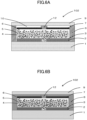


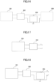
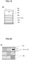


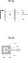


Classifications
-
- B—PERFORMING OPERATIONS; TRANSPORTING
- B01—PHYSICAL OR CHEMICAL PROCESSES OR APPARATUS IN GENERAL
- B01D—SEPARATION
- B01D53/00—Separation of gases or vapours; Recovering vapours of volatile solvents from gases; Chemical or biological purification of waste gases, e.g. engine exhaust gases, smoke, fumes, flue gases, aerosols
- B01D53/26—Drying gases or vapours
-
- H—ELECTRICITY
- H10—SEMICONDUCTOR DEVICES; ELECTRIC SOLID-STATE DEVICES NOT OTHERWISE PROVIDED FOR
- H10K—ORGANIC ELECTRIC SOLID-STATE DEVICES
- H10K30/00—Organic devices sensitive to infrared radiation, light, electromagnetic radiation of shorter wavelength or corpuscular radiation
- H10K30/80—Constructional details
- H10K30/81—Electrodes
- H10K30/82—Transparent electrodes, e.g. indium tin oxide [ITO] electrodes
-
- H—ELECTRICITY
- H10—SEMICONDUCTOR DEVICES; ELECTRIC SOLID-STATE DEVICES NOT OTHERWISE PROVIDED FOR
- H10K—ORGANIC ELECTRIC SOLID-STATE DEVICES
- H10K30/00—Organic devices sensitive to infrared radiation, light, electromagnetic radiation of shorter wavelength or corpuscular radiation
- H10K30/80—Constructional details
- H10K30/88—Passivation; Containers; Encapsulations
-
- H—ELECTRICITY
- H10—SEMICONDUCTOR DEVICES; ELECTRIC SOLID-STATE DEVICES NOT OTHERWISE PROVIDED FOR
- H10K—ORGANIC ELECTRIC SOLID-STATE DEVICES
- H10K39/00—Integrated devices, or assemblies of multiple devices, comprising at least one organic radiation-sensitive element covered by group H10K30/00
- H10K39/601—Assemblies of multiple devices comprising at least one organic radiation-sensitive element
- H10K39/621—Assemblies of multiple devices comprising at least one organic radiation-sensitive element comprising only organic radiation-sensitive elements
-
- H—ELECTRICITY
- H10—SEMICONDUCTOR DEVICES; ELECTRIC SOLID-STATE DEVICES NOT OTHERWISE PROVIDED FOR
- H10K—ORGANIC ELECTRIC SOLID-STATE DEVICES
- H10K77/00—Constructional details of devices covered by this subclass and not covered by groups H10K10/80, H10K30/80, H10K50/80 or H10K59/80
- H10K77/10—Substrates, e.g. flexible substrates
-
- H—ELECTRICITY
- H10—SEMICONDUCTOR DEVICES; ELECTRIC SOLID-STATE DEVICES NOT OTHERWISE PROVIDED FOR
- H10K—ORGANIC ELECTRIC SOLID-STATE DEVICES
- H10K85/00—Organic materials used in the body or electrodes of devices covered by this subclass
- H10K85/10—Organic polymers or oligomers
-
- H—ELECTRICITY
- H10—SEMICONDUCTOR DEVICES; ELECTRIC SOLID-STATE DEVICES NOT OTHERWISE PROVIDED FOR
- H10K—ORGANIC ELECTRIC SOLID-STATE DEVICES
- H10K30/00—Organic devices sensitive to infrared radiation, light, electromagnetic radiation of shorter wavelength or corpuscular radiation
- H10K30/10—Organic devices sensitive to infrared radiation, light, electromagnetic radiation of shorter wavelength or corpuscular radiation comprising heterojunctions between organic semiconductors and inorganic semiconductors
- H10K30/15—Sensitised wide-bandgap semiconductor devices, e.g. dye-sensitised TiO2
-
- H—ELECTRICITY
- H10—SEMICONDUCTOR DEVICES; ELECTRIC SOLID-STATE DEVICES NOT OTHERWISE PROVIDED FOR
- H10K—ORGANIC ELECTRIC SOLID-STATE DEVICES
- H10K39/00—Integrated devices, or assemblies of multiple devices, comprising at least one organic radiation-sensitive element covered by group H10K30/00
- H10K39/10—Organic photovoltaic [PV] modules; Arrays of single organic PV cells
-
- Y—GENERAL TAGGING OF NEW TECHNOLOGICAL DEVELOPMENTS; GENERAL TAGGING OF CROSS-SECTIONAL TECHNOLOGIES SPANNING OVER SEVERAL SECTIONS OF THE IPC; TECHNICAL SUBJECTS COVERED BY FORMER USPC CROSS-REFERENCE ART COLLECTIONS [XRACs] AND DIGESTS
- Y02—TECHNOLOGIES OR APPLICATIONS FOR MITIGATION OR ADAPTATION AGAINST CLIMATE CHANGE
- Y02E—REDUCTION OF GREENHOUSE GAS [GHG] EMISSIONS, RELATED TO ENERGY GENERATION, TRANSMISSION OR DISTRIBUTION
- Y02E10/00—Energy generation through renewable energy sources
- Y02E10/50—Photovoltaic [PV] energy
- Y02E10/549—Organic PV cells
Definitions
- the disclosures herein generally relate to a photoelectric conversion element, a photoelectric conversion module, an electronic device, and a partition.
- a photoelectric conversion element which has a high translucency and includes, as electrode materials, a conductive transparent material, such as a silver nanowire, and a conductive transparent polymer that are highly translucent materials, has been proposed (see, for example, Japanese Unexamined Patent Application Publication No. 2017-175019 ).
- an organic thin film solar cell element which includes an adhesive layer obtained by curing a photocurable resin or a thermosetting resin so that the resin covers the whole photoelectric conversion layer, has been proposed (see, for example, Japanese Unexamined Patent Application Publication No. 2013-168572 ).
- a photoelectric conversion element includes: a first substrate; a first electrode; a photoelectric conversion layer; a second electrode; a sealing part; and a second substrate.
- the photoelectric conversion element is translucent.
- the second electrode includes a conductive nanowire and a conductive polymer.
- the sealing part includes a drying agent.
- a photoelectric conversion element of the present disclosure includes: a first substrate; a first electrode; a photoelectric conversion layer; a second electrode; a sealing part; and a second substrate.
- the photoelectric conversion element is translucent.
- the photoelectric conversion element includes a hole blocking layer, an electrode protection layer, and other layers if necessary.
- the second electrode in the photoelectric conversion element of the present disclosure includes a conductive nanowire and a conductive polymer.
- the sealing part in the photoelectric conversion element of the present disclosure includes a drying agent.
- An object of the present disclosure is to provide a photoelectric conversion element excellent in durability.
- the "photoelectric conversion element” means an element that converts light energy into electric energy or an element that converts electric energy into light energy. Specific examples thereof include solar cells and photodiodes.
- a "layer” may be a single film (single layer), or may be a stacked layer in which a plurality of films is stacked.
- a “layered direction” means a direction perpendicular to a surface of a layer in a photoelectric conversion element.
- the "connection” means not only physical contact but also electric connection enough to be able to achieve the effect of the present disclosure.
- a conventional photoelectric conversion element including electrodes formed of a metal nanowire and a conductive polymer has such a problem that moisture derived from an electrode coating liquid for forming electrodes remains inside the electrodes, and this moisture deteriorates the durability of the photoelectric conversion element itself.
- the present inventors found that inclusion of the drying agent in the sealing material in the photoelectric conversion element can remove the moisture derived from the electrode coating liquid and can improve the durability of the photoelectric conversion element.
- a visible light transmittance of the photoelectric conversion element itself of the present disclosure is preferably 15% or more, more preferably 20% or more, and still more preferably 20% or more and 50% or less. When the visible light transmittance of the photoelectric conversion element itself is 20% or more and 50% or less, excellent durability can be obtained.
- Conventional photoelectric conversion elements have the following problem. Specifically, when a second electrode is produced through deposition of silver, a photoelectric conversion element has an extremely low visible light transmittance, and almost no translucency is achieved. As a result, almost no electric power is generated unless light is emitted from a side of a first electrode, which makes it difficult to generate electric power under low illuminance (1,500 lx or less) conditions such as indoor environments.
- the visible light transmittance of the photoelectric conversion element itself is 15% or more, transmission of visible light is ensured, and a photoelectric conversion element that can generate electric power even under low illuminance (1,500 lx or less) conditions such as indoor environments can be obtained by receiving light from both surfaces of the first electrode side and the second electrode side.
- the photoelectric conversion element of the present disclosure can receive light from both surfaces of the first electrode side and the second electrode side, the photoelectric conversion element of the present disclosure can obtain more excellent durability under living space conditions (under low illuminance) compared to conventional photoelectric conversion elements including a second electrode formed through deposition of silver.
- Having a translucency means that a transmittance of visible light having a wavelength of 380 nm or more and 780 nm or less is 15% or more, the transmittance being measured in a layered direction of a photoelectric conversion element according to JIS A5759.
- the visible light transmittance is a transmittance of visible light having a wavelength of 380 nm or more and 780 nm or less according to JIS A5759, and can be measured by a measurement method of visible light transmittance t ⁇ using, for example, an ultraviolet and visible spectrophotometer (apparatus name: ISR-3100, manufactured by SHIMADZU CORPORATION.
- a photoelectric conversion element of the present disclosure includes a first substrate and a second substrate.
- the first substrate is a substrate provided on the outermost part of a first electrode side
- the second substrate is a substrate provided on the outermost part of a second electrode side.
- the first substrate and the second substrate may be collectively referred to as "substrate”.
- the photoelectric conversion element of the present disclosure may be an aspect where one of the first substrate and the second substrate is provided.
- the shape, structure, and size of the substrate are not particularly limited and may be appropriately selected in accordance with the intended purpose.
- the material of the first substrate is not particularly limited and may be appropriately selected in accordance with the intended purpose as long as it is translucent and has an insulation property.
- Examples thereof include substrates such as glass, plastic films, and ceramic.
- a substrate having heat resistance to a firing temperature is preferable.
- preferable examples of the substrate include those that are flexible.
- the second substrate is not particularly limited and conventional products can be used. Examples thereof include substrates such as glass, plastic films, and ceramic. Among them, plastic films are more preferable.
- a convex-concave part may be formed at a connection part between the second substrate and a sealing part that will be described later, in order to increase adhesiveness.
- a method of forming the convex-concave part is not particularly limited and may be appropriately selected in accordance with the intended purpose.
- Examples of the formation method include sand blasting, water blasting, abrasive paper, chemical etching, and laser processing.
- organic matter on the surface may be removed, or hydrophilicity may be improved.
- the method of removing organic matter from the surface of the second substrate is not particularly limited and may be appropriately selected in accordance with the intended purpose.
- Examples of the method include UV ozone washing and oxygen plasma treatment.
- a water vapor transmittance of the second substrate is not particularly limited and may be appropriately selected in accordance with the intended purpose.
- the water vapor transmittance is preferably 0.01 (g/m 2 ⁇ day) or less, and more preferably 0.001 (g/m 2 ⁇ day) or less.
- the durability under high humidity and high temperature of 40°C and 90%RH or more can be improved.
- the water vapor transmittance of the second substrate is 0.001(g/m 2 ⁇ day) or less, the durability under high humidity and high temperature of 60°C and 90%RH or more can be improved.
- the water vapor transmittance can be measured through, for example, gas chromatography according to JIS K 7129.
- the second substrate may be formed of a single layer or may be formed of such a structure that a plurality of layers is stacked.
- the second substrate is preferably formed of such a structure that a plurality of layers is stacked.
- Examples of the structure that a plurality of layers is stacked include: such a structure that a substrate for protection from external impact and a barrier layer for decreasing the water vapor transmittance are stacked; and such a structure that 100 or more thin films each having a thickness on the nanometer scale are stacked on top of one another.
- the photoelectric conversion element includes a first electrode.
- the shape and size of the first electrode are not particularly limited and may be appropriately selected in accordance with the intended purpose.
- the visible light transmittance of the first electrode is preferably 60% or more.
- the visible light transmittance of the first electrode can be determined by measuring, for example, the first electrode formed on the first substrate by a measurement method of visible light transmittance t ⁇ using an ultraviolet and visible spectrophotometer (apparatus name: ISR-3100, manufactured by SHIMADZU CORPORATION) according to JIS A5759.
- ISR-3100 manufactured by SHIMADZU CORPORATION
- the structure of the first electrode is not particularly limited and may be appropriately selected in accordance with the intended purpose.
- the structure may be a single layer structure or a structure in which a plurality of materials is stacked.
- the material of the first electrode is not particularly limited and may be appropriately selected in accordance with the intended purpose as long as it is transparent to visible light and is conductive. Examples thereof include transparent conductive metal oxides, carbon material, and metals.
- transparent conductive metal oxide examples include indium-tin oxide (referred to as "ITO” hereinafter), fluorine-doped tin oxide (referred to as “FTO” hereinafter), antimony-doped tin oxide (referred to as “ATO” hereinafter), niobium-doped tin oxide (referred to as “NTO” hereinafter), aluminum-doped zinc oxide, indium-zinc oxide, and niobiumtitanium oxide.
- ITO indium-tin oxide
- FTO fluorine-doped tin oxide
- ATO antimony-doped tin oxide
- NTO niobium-doped tin oxide
- aluminum-doped zinc oxide indium-zinc oxide
- niobiumtitanium oxide examples include aluminum-doped zinc oxide, indium-zinc oxide, and niobiumtitanium oxide.
- Examples of the carbon include carbon black, carbon nanotube, graphene, and fullerene.
- Examples of the metal include gold, silver, aluminum, nickel, indium, tantalum, and titanium.
- transparent conductive metal oxide having high transparency is preferable, and ITO, FTO, ATO, and NTO are more preferable.
- An average thickness of the first electrode is not particularly limited and may be appropriately selected in accordance with the intended purpose.
- the average thickness of the first electrode is preferably 5 nm or more and 100 ⁇ m or less, and more preferably 50 nm or more and 10 ⁇ m or less.
- the average thickness of the first electrode is preferably an average thickness enough to obtain translucency.
- the first electrode can be formed by conventional methods such as the sputtering method, the vapor deposition method, and the spray method.
- the first electrode is preferably formed on the first substrate. It is possible to use a commercially available integrated product where the first electrode has been formed on the first substrate in advance.
- Examples of the commercially available integrated product where the first electrode is formed on the first substrate include FTO-coated glass (for example, product name: TEC15, manufactured by Nippon Electric Glass Co., Ltd.), ITO-coated glass (for example, manufactured by GEOMATEC Co., Ltd.), zinc oxide/aluminum coated glass, FTO-coated transparent plastic films, and ITO-coated transparent plastic films (for example, manufactured by GEOMATEC Co., Ltd.).
- FTO-coated glass for example, product name: TEC15, manufactured by Nippon Electric Glass Co., Ltd.
- ITO-coated glass for example, manufactured by GEOMATEC Co., Ltd.
- zinc oxide/aluminum coated glass for example, FTO-coated transparent plastic films
- ITO-coated transparent plastic films for example, manufactured by GEOMATEC Co., Ltd.
- glass substrates provided with a transparent electrode where tin oxide or indium oxide is doped with a cation or an anion having a different atomic value examples include: glass substrates provided with a transparent electrode where tin oxide or indium oxide is doped with a cation or an anion having a different atomic value; and glass substrates provided with a metal electrode having such a structure that allows light in the form of a mesh or stripes to pass.
- a metal lead wire may be used in combination in order to decrease an electric resistance value.
- Examples of materials of the metal lead wire include aluminum, copper, silver, gold, platinum, and nickel.
- the metal lead wire can be used in combination by forming the metal lead wire on a substrate through, for example, vapor deposition, sputtering, or pressure bonding, and providing a layer of ITO or FTO thereon.
- the photoelectric conversion element preferably includes a hole blocking layer.
- the hole blocking layer is formed between the first electrode and an electron transport layer that will be described hereinafter.
- the hole blocking layer is very effective in improving output and its persistence.
- the hole blocking layer includes a photosensitization compound, transports, to a first electrode, electrons transported to an electron transport layer, and minimizes contact with a hole transport layer. As a result, the hole blocking layer does not easily allow holes to flow to the first electrode and can minimize reductions in output due to recombining of electrons and holes.
- a solid photoelectric conversion element including the hole transport layer has much greater effects achieved by formation of the hole blocking layer than a wet photoelectric conversion element including an electrolyte because of a higher recombining speed of holes in the hole transport material and electrons on the surface of the electrode.
- the material of the hole blocking layer is not particularly limited and may be appropriately selected in accordance with the intended purpose as long as it is transparent to visible light and an electron transport property.
- Examples thereof include: semiconductors of simple substances such as silicon and germanium; compound semiconductors such as chalcogenides of metal, and compounds having a perovskite structure.
- Examples of the chalcogenide of metal include: oxides of titanium, tin, zinc, iron, tungsten, zirconium, hafnium, strontium, indium, cerium, yttrium, lanthanum, vanadium, niobium, and tantalum; sulfides of cadmium, zinc, lead, silver, antimony, and bismuth; selenide of cadmium and lead; and tellurides of cadmium.
- Examples of other compound semiconductors include: phosphides of zinc, gallium, indium, and cadmium; gallium arsenide, copper-indium selenide, and copper-indium sulfide.
- Examples of the compound having a perovskite structure include strontium titanate, calcium titanate, sodium titanate, barium titanate, and potassium niobate.
- an oxide semiconductor is preferable, titanium oxide, niobium oxide, magnesium oxide, aluminum oxide, zinc oxide, tungsten oxide, and tin oxide are more preferable, and titanium oxide is still more preferable.
- the crystal type of these semiconductors is not particularly limited and may be appropriately selected in accordance with the intended purpose.
- the crystal type may be a single crystal, a polycrystal, or an amorphous crystal.
- a method of producing the hole blocking layer is not particularly limited and may be appropriately selected in accordance with the intended purpose. Examples thereof include a method in which a thin film is formed in vacuum (vacuum film formation method); and a wet film formation method.
- Examples of the vacuum film formation method include the sputtering method, the pulse laser deposition method (PLD method), the ion beam sputtering method, the ion assisted deposition method, the ion plating method, the vacuum deposition method, the atomic layer deposition method (ALD method), and the chemical vapor deposition method (CVD method).
- PLD method pulse laser deposition method
- ion beam sputtering method the ion assisted deposition method
- the ion plating method the vacuum deposition method
- ALD method atomic layer deposition method
- CVD method chemical vapor deposition method
- Examples of the wet film formation method include a sol-gel method.
- the sol-gel method is the following method. Specifically, a solution is allowed to undergo a chemical reaction, such as hydrolysis or polymerization ⁇ condensation, to prepare a gel. Then, the gel is subjected to a heat treatment to facilitate compactness.
- a method of coating the sol solution is not particularly limited and may be appropriately selected in accordance with the intended purpose. Examples thereof include the dip method, the spray method, the wire bar method, the spin coating method, the roller coating method, the blade coating method, the gravure coating method, and wet printing methods such as relief printing, offset printing, gravure printing, intaglio printing, rubber plate printing, and screen printing.
- a temperature at which the heat treatment is performed after the sol solution is coated is preferably 80°C or more, and more preferably 100°C or more.
- the average thickness of the hole blocking layer is not particularly limited and may be appropriately selected in accordance with the intended purpose.
- the average thickness is preferably 5 nm or more and 1 ⁇ m or less.
- the average thickness is more preferably 500 nm or more and 700 nm or less.
- the average thickness is more preferably 5 nm or more and 30 nm or less.
- the photoelectric conversion layer includes an electron transport layer and a hole transport layer, and includes other layers if necessary.
- the photoelectric conversion layer may be a single layer or a multilayer in which a plurality of layers is stacked.
- the photoelectric conversion layer preferably includes a basic compound.
- the basic compound is included in any of layers constituting the photoelectric conversion layer, but is preferably included in, for example, the hole transport layer.
- the photoelectric conversion element includes an electron transport layer.
- the electron transport layer is formed for the purpose of transporting generated electrons to the hole blocking layer. Therefore, the electron transport layer is preferably disposed adjacent to the hole blocking layer.
- the structure of the electron transport layer is not particularly limited and may be appropriately selected in accordance with the intended purpose.
- the electron transport layers are not continuous and are separated. Separation of the electron transport layers is advantageous because diffusion of electrons is minimized to decrease leak current, resulting in improvement of photodurability.
- the structure of the electron transport layer may be a continuous single layer or a multilayer in which a plurality of layers is stacked.
- the electron transport layer includes an electron transport material, preferably includes a photosensitization compound, and includes, if necessary, other materials.
- the electron transport material is not particularly limited and may be appropriately selected in accordance with the intended purpose.
- the electron transport material is preferably a semiconductor material.
- the semiconductor material has a particulate shape, and these particles are joined to form a porous film.
- a photosensitization compound is chemically or physically adsorbed.
- the electron transport layer is porous, the amount of the photosensitization compound adsorbed on the surface can be drastically increased, which is effective in achieving high output.
- the semiconductor material is not particularly limited and conventional materials may be used. Examples thereof include semiconductors of simple substances, compound semiconductors, and compounds having a perovskite structure.
- Examples of the semiconductor of the simple substance include silicon and germanium.
- Examples of the compound semiconductor include chalcogenides of metal. Specific examples thereof include oxides of titanium, tin, zinc, iron, tungsten, zirconium, hafnium, strontium, indium, cerium, yttrium, lanthanum, vanadium, niobium, and tantalum; sulfides of cadmium, zinc, lead, silver, antimony, and bismuth; selenides of cadmium and lead; and telluride of cadmium. Examples of other compound semiconductors include phosphides of, for example, zinc, gallium, indium, and cadmium, gallium arsenide, copper-indium selenide, and copper-indium sulfide.
- Examples of the compound having a perovskite structure include strontium titanate, calcium titanate, sodium titanate, barium titanate, and potassium niobate.
- an oxide semiconductor is preferable, and titanium oxide, zinc oxide, tin oxide, and niobium oxide are more preferable.
- the electron transport material of the electron transport layer is titanium oxide, a high open circuit voltage can be obtained because of its high conduction band level, resulting in high photoelectric conversion characteristics, which is advantageous.
- titanium oxide has a high refractive index, a light confinement effect can be achieved, which makes it possible to obtain a high short circuit current.
- titanium oxide has high permittivity and high mobility, a high fill factor can be obtained, which is advantageous.
- the crystal type of the semiconductor material is not particularly limited and may be appropriately selected in accordance with the intended purpose.
- the crystal type may be a single crystal, a polycrystal, or an amorphous crystal.
- a number average particle diameter of primary particles of the semiconductor material is not particularly limited and may be appropriately selected in accordance with the intended purpose.
- the number average particle diameter is preferably 1 nm or more and 100 nm or less, and more preferably 5 nm or more and 50 nm or less.
- a semiconductor material having a number average particle diameter that is larger than the above upper limit of the number average particle diameter may be mixed or stacked. Such a semiconductor material can produce the effect of scattering incident light to improve conversion efficiency.
- the number average particle diameter is preferably 50 nm or more and 500 nm or less.
- An average thickness of the electron transport layer is not particularly limited and may be appropriately selected in accordance with the intended purpose.
- the average thickness is preferably 50 nm or more and 100 ⁇ m or less, more preferably 100 nm or more and 50 ⁇ m or less, and still more preferably 120 nm or more and 10 ⁇ m or less.
- An average thickness of the electron transport layer falling within the preferable range is advantageous because an amount of the photosensitization compound per unit projection area can be sufficiently secured, a high light trapping rate can be maintained, the diffusion distance of injected electrons does not easily increase, and the loss caused due to recombining of electric charges can be decreased.
- a method of producing the electron transport layer is not particularly limited and may be appropriately selected in accordance with the intended purpose. Examples thereof include: a method in which a thin film is formed in vacuum such as sputtering; a wet film formation method; and a wet printing method. Among them, in terms of production costs, the wet film formation method is preferable, and a method, in which paste (dispersion liquid of the semiconductor material) obtained by dispersing powder or sol of the semiconductor material is prepared and is coated on the first electrode as an electron collecting electrode substrate or on the hole blocking layer, is more preferable.
- the wet film formation method is not particularly limited and may be appropriately selected in accordance with the intended purpose. Examples thereof include the dip method, the spray method, the wire bar method, the spin coating method, the roller coating method, the blade coating method, the gravure coating method, and the die coating method.
- the wet printing method is not particularly limited and may be appropriately selected in accordance with the intended purpose.
- various methods such as relief printing, offset printing, gravure printing, intaglio printing, rubber plate printing, and screen printing can be used.
- Examples of a method of preparing the dispersion liquid of the semiconductor material include a mechanically pulverizing method using, for example, a conventional milling device. This method makes it possible to prepare a dispersion liquid of a semiconductor material by dispersing, in water or a solvent, a particulate semiconductor material alone or a mixture of a semiconductor material and a resin.
- the resin is not particularly limited and may be appropriately selected in accordance with the intended purpose.
- examples thereof include polymers or copolymers of vinyl compounds such as styrene, vinyl acetate, acrylic ester, and methacrylate, silicon resins, phenoxy resins, polysulfone resins, polyvinyl butyral resins, polyvinyl formal resins, polyester resins, cellulose ester resins, cellulose ether resins, urethane resins, phenol resins, epoxy resins, polycarbonate resins, polyarylate resins, polyamide resins, and polyimide resins. These may be used alone or in combination.
- the solvent is not particularly limited and may be appropriately selected in accordance with the intended purpose. Examples thereof include water, alcohol solvents, ketone solvents, ester solvents, ether solvents, amide solvents, halogenated hydrocarbon solvents, and hydrocarbon solvents.
- alcohol solvent examples include methanol, ethanol, isopropyl alcohol, and ⁇ -terpineol.
- ketone solvent examples include acetone, methyl ethyl ketone, and methyl isobutyl ketone.
- ester solvent examples include ethyl formate, ethyl acetate, and n-butyl acetate.
- ether solvent examples include diethyl ether, dimethoxy ethane, tetrahydrofuran, dioxolane, and dioxane.
- amide solvent examples include N,N-dimethylformamide, N,N-dimethylacetoamide, and N-methyl-2-pyrrolidone.
- halogenated hydrocarbon solvent examples include dichloromethane, chloroform, bromoform, methyl iodide, dichloroethane, trichloroethane, trichloroethylene, chlorobenzene, o-dichlorobenzene, fluorobenzene, bromobenzene, iodobenzene, and 1-chloronaphthalene.
- hydrocarbon solvent examples include n-pentane, n-hexane, n-octane, 1,5-hexadiene, cyclohexane, methylcyclohexane, cyclohexadiene, benzene, toluene, o-xylene, m-xylene, p-xylene, ethylbenzene, and cumene.
- acid In order to minimize reaggregation of particles, acid, a surfactant, a chelating agent, or the like may be added to the dispersion liquid including the semiconductor material or the paste including the semiconductor material obtained through, for example, the sol-gel method.
- Examples of the acid include hydrochloric acid, nitric acid, and acetic acid.
- surfactant examples include polyoxyethylene octylphenyl ether.
- chelating agent examples include acetylacetone, 2-aminoethanol, and ethylenediamine.
- addition of a thickener is an effective means.
- thickener examples include polyethylene glycol, polyvinyl alcohol, and ethyl cellulose.
- particles of the semiconductor material may be electronically brought into contact with each other, the semiconductor material may be fired to improve the film strength or adhesiveness to a substrate, microwave or electron beams may be emitted, or laser light may be emitted. These treatments may be performed alone or in combination.
- the firing temperature is not particularly limited and may be appropriately selected in accordance with the intended purpose. If the temperature is too high, a substrate may have a high resistance and melting may occur. Therefore, the firing temperature is preferably 30°C or more and 700°C or less, and more preferably 100°C or more and 600°C or less.
- the firing time is not particularly limited and may be appropriately selected in accordance with the intended purpose. The firing time is preferably 10 minutes or more and 10 hours or less.
- the irradiation time is not particularly limited and may be appropriately selected in accordance with the intended purpose.
- the irradiation time is preferably 1 hour or less. In this case, irradiation may be performed from a surface side where the electron transport layer is formed, or irradiation may be performed from a surface side where no electron transport layer is formed.
- a chemical plating treatment using a mixed solution of a titanium tetrachloride aqueous solution and an organic solvent or an electrochemical plating treatment using a titanium trichloride aqueous solution may be performed in order to increase the surface area of the electron transport layer or to enhance the electron injection efficiency from a photosensitization compound that will be described hereinafter to the semiconductor material.
- a film obtained by firing the semiconductor material having a diameter of several tens of nanometers may be porous.
- Such a porous nanostructure has a considerably high surface area, and the surface area can be represented by a roughness factor.
- the roughness factor is a numerical value representing an actual area of the porous inner part relative to an area of the semiconductor particles coated on the first substrate. Therefore, the roughness factor is preferably larger, but is preferably 20 or more in relation to an average thickness of the electron transport layer.
- the particles of the electron transport material may be doped with a lithium compound.
- a solution of a lithium bis(trifluoromethanesulfonimide) compound is deposited on particles of the electron transport material through, for example, spin coating, followed by firing.
- the lithium compound is not particularly limited and may be appropriately selected in accordance with the intended purpose. Examples thereof include lithium bis(trifluoromethanesulfonimide), lithium bis(fluoromethanesulfonimide), lithium bis(fluoromethanesulfonyl)(trifluoromethanesulfonyl)imide, lithium perchlorate, and lithium iodide.
- the photosensitization compound is preferably provided on the electron transport layer.
- the photosensitization compound compounds that can further improve the output or photoelectric conversion efficiency can be used.
- the photosensitization compound is preferably adsorbed on the surface of the semiconductor material constituting the electron transport layer.
- the photosensitization compound is not particularly limited and may be appropriately selected in accordance with the intended purpose as long as it is photoexcited by light to be applied to the photoelectric conversion element. Examples thereof include the following conventional compounds.
- Specific examples thereof include: metal complex compounds described in, for example, Japanese Translation of PCT International Application Publication No. 7-500630 , Japanese Unexamined Patent Application Publication No. 10-233238 , Japanese Unexamined Patent Application Publication No. 2000-26487 , Japanese Unexamined Patent Application Publication No. 2000-323191 , and Japanese Unexamined Patent Application Publication No. 2001-59062 ; coumarin compounds described in, for example, Japanese Unexamined Patent Application Publication No. 10-93118 , Japanese Unexamined Patent Application Publication No. 2002-164089 , Japanese Unexamined Patent Application Publication No. 2004-95450 , and J. Phys. Chem. C, 7224, Vol.
- metal complex compounds metal complex compounds, coumarin compounds, polyene compounds, indoline compounds, and thiophene compounds are preferable, and compounds expressed by the following Structural Formulas (1), (2), and (3) manufactured by Mitsubishi Paper Mills Limited are preferable.
- One example of a photosensitization compound that is more preferably used is, for example, a compound having the following Formula (5).
- X 11 and X 12 each independently represent an oxygen atom, a sulfur atom, or a selenium atom.
- R 11 represents a methine group that may have a substituent.
- substituents include: aryl groups such as a phenyl group and a naphthyl group; and heterocycles such as a thienyl group and a furyl group.
- R 12 represents an alkyl group, an aryl group, or a heterocycle group, each of which may have a substituent.
- alkyl group include a methyl group, an ethyl group, a 2-propyl group, and a 2-ethylhexyl group.
- aryl group and the heterocycle group are exemplified above.
- R 13 represents an acidic group such as carboxylic acid, sulfonic acid, phosphonic acid, boronic acid, or phenols.
- R 13 may be one substituent or may be two or more substituents.
- Z 1 and Z 2 each independently represent a substituent that forms a cyclic structure.
- examples of the Z 1 include condensed hydrocarbon-based compounds such as a benzene ring and a naphthalene ring; and heterocycles such as a thiophene ring and a furan ring, each of which may have a substituent.
- Specific examples of the substituent include: the aforementioned alkyl groups; and alkoxy groups such as a methoxy group, an ethoxy group, and a 2-isopropoxy group.
- Examples of a part including Z 2 , a benzene ring fused to Z 2 , and R 12 include the following (A-1) to (A-22).
- m represents an integer of from 0 through 2.
- a compound represented by the following Formula (6) is more preferably used.
- n represents an integer of 0 or 1
- R 3 represent an aryl group that may have a substituent or one substituent selected from substituents expressed by the following three Structural Formulas.
- photosensitization compounds including Formula (5) and Formula (6) described above include the following (B-1) to (B-41), but are not limited thereto.
- examples of preferably used photosensitization compounds also include compounds including the following Formula (7).
- Ar 1 and Ar 2 represent an aryl group that may have a substituent.
- R 1 and R 2 represent a straight-chain or branched alkyl group having from 4 through 10 carbon atoms.
- X represents a substituent expressed by any one of the following Structural Formulas.
- a compound represented by the following Formula (8) is more preferably used.
- Ar 4 and Ar 5 represent a phenyl group that may have a substituent or a naphthyl group that may have a substituent.
- Ar 6 represents a phenyl group that may have a substituent or a thiophene group that may have a substituent.
- Ar 7 and Are represent a phenyl group that may have a substituent or a naphthyl group that may have a substituent.
- Ar 9 represents a phenyl group that may have a substituent or a thiophene group that may have a substituent.
- photosensitization compound represented by Formula (9) include exemplified compounds (B-59) to (B-62) as presented below, but the photosensitization compound of the present disclosure is not limited thereto.
- One kind of the photosensitization compound or two kinds or more of the photosensitization compounds may be included.
- a LED light source used as a light source has different colors such as warm colors, cold colors, or white color.
- the spectra differ depending on colors.
- a color temperature of 3,000 K results in a relatively strong wavelength in a region of 600 nm, exhibiting a reddish light bulb color.
- a color temperature of 5,000 K results in a well-balanced neutral white color as a whole.
- a color temperature of more than 6,500 K results in a relatively strong wavelength in a region of 450 nm, exhibiting a bluish daylight color.
- the photoelectric conversion element can preferably maintain high output even when an LED having a different color temperature is used.
- inclusion of mixed photosensitization compounds different in absorption wavelength in the photoelectric conversion layer is effective because the output difference caused by color temperatures can be decreased.
- Examples of a method of adsorbing the photosensitization compound on the surface of the semiconductor material of the electron transport layer include: a method in which the electron transport layer including the semiconductor material is immersed in a solution of the photosensitization compound or a dispersion liquid of the photosensitization compound; and a method in which a solution of the photosensitization compound or a dispersion liquid of the photosensitization compound is coated and adsorbed on the electron transport layer.
- any of the following methods may be used: the immersion method, the dip method, the roller method, or the air knife method.
- any of the following methods may be used: the wire bar method, the slide hopper method, the extrusion method, the curtain method, the spin method, or the spray method.
- the photosensitization compound can be adsorbed in a supercritical fluid including carbon dioxide.
- a condensation agent When the photosensitization compound is adsorbed on the semiconductor material, a condensation agent may be used in combination.
- the condensation agent may be a substance exhibiting a catalytic action that physically or chemically binds the photosensitization compound on the surface of the semiconductor material, or may be a substance that acts stoichiometrically and advantageously transfers chemical equilibrium.
- thiol or a hydroxy compound may be added as an auxiliary condensation agent.
- solvents that dissolve or disperse the photosensitization compound include water, alcohol solvents, ketone solvents, ester solvents, ether solvents, amide solvents, halogenated hydrocarbon solvents, hydrocarbon solvents, and other solvents.
- Examples of the alcohol solvent include methanol, ethanol, isopropyl alcohol, and t-butanol.
- ketone solvent examples include acetone, methyl ethyl ketone, and methyl isobutyl ketone.
- ester solvent examples include ethyl formate, ethyl acetate, and n-butyl acetate.
- ether solvent examples include diethyl ether, dimethoxy ethane, tetrahydrofuran, dioxolane, and dioxane.
- amide solvent examples include N,N-dimethylformamide, N,N-dimethylacetoamide, and N-methyl-2-pyrrolidone.
- halogenated hydrocarbon solvent examples include dichloromethane, chloroform, bromoform, methyl iodide, dichloroethane, trichloroethane, trichloroethylene, chlorobenzene, o-dichlorobenzene, fluorobenzene, bromobenzene, iodobenzene, and 1-chloronaphthalene.
- hydrocarbon solvent examples include n-pentane, n-hexane, n-octane, 1,5-hexadiene, cyclohexane, methylcyclohexane, cyclohexadiene, benzene, toluene, o-xylene, m-xylene, p-xylene, ethylbenzene, and cumene.
- Examples of the other solvents include acetonitrile.
- the photosensitization compound may work more effectively depending on its kind when aggregation between the compounds is minimized. Therefore, an aggregation dissociation agent may be used in combination.
- the aggregation dissociation agent is not particularly limited and may be appropriately selected in accordance with a dye to be used.
- a dye to be used Preferable examples thereof include steroid compounds such as cholic acid and chenodeoxycholic acid, long chain alkylcarboxylic acid, and long chain alkylphosphonic acid.
- the amount of the aggregation dissociation agent is preferably 0.01 parts by mass or more and 500 parts by mass or less, and more preferably 0.1 parts by mass or more and 100 parts by mass or less, relative to 1 part by mass of the photosensitization compound.
- the photosensitization compound, or the photosensitization compound and the aggregation dissociation agent are adsorbed on the surface of the semiconductor material constituting the electron transport layer, its temperature is preferably -50°C or more and 200°C or less.
- the adsorption time is preferably 5 seconds or more and 1,000 hours or less, more preferably 10 seconds or more and 500 hours or less, and still more preferably 1 minute or more and 150 hours or less.
- the adsorption step is preferably performed in a dark place.
- the adsorption step may be performed statically or under stirring.
- the stirring method is not particularly limited and may be appropriately selected in accordance with the intended purpose.
- the method is, for example, a method using, for example, a stirrer, a ball mill, a paint conditioner, a sand mill, an attritor, a disperser, or ultrasonic dispersion.
- the electron transport layer preferably includes a perovskite layer adjacent to the electron transport layer and a bulk heterojunction layer.
- the perovskite layer means a layer that contains a perovskite compound and absorbs light to sensitize the electron transport layer. Therefore, the perovskite layer is preferably disposed adjacent to the electron transport layer.
- the shape and size of the perovskite layer are not particularly limited and may be appropriately selected in accordance with the intended purpose.
- the perovskite compound is a complex substance of an organic compound and an inorganic compound, and is represented by the following Formula (X).
- a ratio of ( ⁇ : ⁇ : ⁇ is 3:1:1; ⁇ and ⁇ are each an integer of more than 1; X represents halogen; Y represents an organic compound including an amino group; and Z represents a metal ion.
- X in Formula (X) is not particularly limited and may be appropriately selected in accordance with the intended purpose. Examples thereof include halogen such as chlorine, bromine, and iodine. These may be used alone or in combination.
- Y in the above Formula (X) is not particularly limited and may be appropriately selected in accordance with the intended purpose as long as it is an organic cation.
- examples thereof include: ions of alkyl amine compounds (e.g., methyl amine, ethyl amine, n-butylamine, and formamidine); and inorganic alkali metal cations (e.g., antimony ions, cesium ions, potassium ions, and rubidium ions). These may be used alone or in combination.
- the inorganic alkali metal cation and the organic cation may be each used in combination. Among them, an organic compound including an amino group (an ion of an alkyl amine compound) is preferable.
- a peak ⁇ max of the optical absorption spectrum is about 350 nm when the halogen ion is Cl, the peak ⁇ max is about 410 nm when the halogen ion is Br, and the peak ⁇ max is about 540 nm when the halogen ion is I.
- the peak ⁇ max is shifted to a longer wavelength side, so a usable spectrum width (band width) varies.
- Z in the above Formula (X) is not particularly limited and may be appropriately selected in accordance with the intended purpose.
- examples thereof include ions of metals such as lead, indium, antimony, tin, copper, and bismuth. These may be used alone or in combination.
- the perovskite layer preferably has a stacked perovskite structure where a layer formed of metal halide and a layer of arranged organic cation molecules are stacked on top of one another.
- An average film thickness of the perovskite layer is 50 nm or more and 2 ⁇ m or less, and more preferably 100 nm or more and 600 nm or less.
- a method of forming the perovskite layer is not particularly limited and may be appropriately selected in accordance with the intended purpose.
- Examples of the method include a method in which a solution obtained by dissolving or dispersing, for example, metal halide and halogenated alkylamine or cesium halide is coated, followed by drying.
- examples of the method of forming the perovskite layer include a two-step precipitation method as described below. Specifically, for example, a solution obtained by dissolving or dispersing metal halide is coated, followed by drying. Then, the dried product is immersed in a solution obtained by dissolving halogenated alkylamine, to form the perovskite compound.
- examples of the method of forming the perovskite layer include a method in which a poor solvent (solvent having a small solubility) for the perovskite compound is added while a solution obtained by dissolving or dispersing, for example, metal halide and halogenated alkylamine is coated thereon, to precipitate crystals.
- a poor solvent solvent having a small solubility
- examples of the method of forming the perovskite layer include a method in which metal halide is deposited in a gas filled with, for example, methylamine.
- a poor solvent for the perovskite compound is added while a solution obtained by dissolving or dispersing, for example, metal halide and halogenated alkylamine is coated thereon, to precipitate crystals.
- a method of coating the solution is not particularly limited and may be appropriately selected in accordance with the intended purpose. Examples of the method include the immersion method, the spin coating method, the spray method, the dip method, the roller method, and the air knife method. As the method of coating the solution, a method of performing precipitation in a supercritical fluid using, for example, carbon dioxide may be used.
- the perovskite layer may include a photosensitization dye (photosensitization compound).
- a method of forming the perovskite layer including the photosensitization dye (photosensitization compound) is not particularly limited and may be appropriately selected in accordance with the intended purpose. Examples of the method include: a method in which the perovskite compound and the photosensitization dye (photosensitization compound) are mixed; and a method in which the perovskite layer is formed, followed by adsorbing the photosensitization dye (photosensitization compound).
- the photosensitization dye (photosensitization compound) is not particularly limited and may be appropriately selected in accordance with the intended purpose, as long as it is a compound photoexcited by excitation light to be used.
- photosensitization dyes include metal complex compounds, coumarin compounds, polyene compounds, indoline compounds, thiophene compounds, cyanine dyes, merocyanine dyes, 9-aryl xanthene compounds, triarylmethane compounds, phthalocyanine compounds, and porphyrin compounds.
- metal complex compounds examples include metal complex compounds described in, for example, Japanese Translation of PCT International Application Publication No. 7-500630 , Japanese Unexamined Patent Application Publication No. 10-233238 , Japanese Unexamined Patent Application Publication No. 2000-26487 , Japanese Unexamined Patent Application Publication No. 2000-323191 , and Japanese Unexamined Patent Application Publication No. 2001-59062 .
- Examples of coumarin compounds include coumarin compounds described in, for example, Japanese Unexamined Patent Application Publication No. 10-93118 , Japanese Unexamined Patent Application Publication No. 2002-164089 , Japanese Unexamined Patent Application Publication No. 2004-95450 , and J. Phys. Chem. C, 7224, Vol. 111 (2007 ).
- polyene compounds examples include polyene compounds described in, for example, Japanese Unexamined Patent Application Publication No. 2004-95450 and Chem. Commun., 4887 (2007 ).
- indoline compounds examples include indoline compounds described in, for example, Japanese Unexamined Patent Application Publication No. 2003-264010 , Japanese Unexamined Patent Application Publication No. 2004-63274 , Japanese Unexamined Patent Application Publication No. 2004-115636 , Japanese Unexamined Patent Application Publication No. 2004-200068 , Japanese Unexamined Patent Application Publication No. 2004-235052 , J. Am. Chem. Soc., 12218, Vol. 126 (2004 ), Chem. Commun., 3036 (2003 ), and Angew. Chem. Int. Ed., 1923, Vol. 47 (2008 ).
- thiophene compounds include thiophene compounds described in, for example, J. Am. Chem. Soc., 16701, Vol. 128 (2006 ) and J. Am. Chem. Soc., 14256, Vol. 128 (2006 ).
- cyanine dyes examples include cyanine dyes described in, for example, Japanese Unexamined Patent Application Publication No. 11-86916 , Japanese Unexamined Patent Application Publication No. 11-214730 , Japanese Unexamined Patent Application Publication No. 2000-106224 , Japanese Unexamined Patent Application Publication No. 2001-76773 , and Japanese Unexamined Patent Application Publication No. 2003-7359 .
- merocyanine dyes examples include merocyanine dyes described in, for example, Japanese Unexamined Patent Application Publication No. 11-214731 , Japanese Unexamined Patent Application Publication No. 11-238905 , Japanese Unexamined Patent Application Publication No. 2001-52766 , Japanese Unexamined Patent Application Publication No. 2001-76775 , and Japanese Unexamined Patent Application Publication No. 2003-7360 .
- 9-aryl xanthene compounds include 9-aryl xanthene compounds described in, for example, Japanese Unexamined Patent Application Publication No. 10-92477 , Japanese Unexamined Patent Application Publication No. 11-273754 , Japanese Unexamined Patent Application Publication No. 11-273755 , and Japanese Unexamined Patent Application Publication No. 2003-31273 .
- triarylmethane compounds examples include triarylmethane compounds described in, for example, Japanese Unexamined Patent Application Publication No. 10-93118 and Japanese Unexamined Patent Application Publication No. 2003-31273 .
- phthalocyanine compounds and porphyrin compounds examples include phthalocyanine compounds and porphyrin compounds described in, for example, Japanese Unexamined Patent Application Publication No. 9-199744 , Japanese Unexamined Patent Application Publication No. 10-233238 , Japanese Unexamined Patent Application Publication No. 11-204821 , Japanese Unexamined Patent Application Publication No. 11-265738 , J. Phys. Chem., 2342, Vol. 91 (1987 ), J. Phys. Chem. B, 6272, Vol. 97 (1993 ), Electroanal. Chem., 31, Vol. 537 (2002 ), Japanese Unexamined Patent Application Publication No. 2006-032260 , J. Porphyrins Phthalocyanines, 230, Vol. 3 (1999 ), Angew. Chem. Int. Ed., 373, Vol. 46 (2007 ), and Langmuir, 5436, Vol. 24 (2008 ).
- metal complex compounds indoline compounds, thiophene compounds, and porphyrin compounds are preferable.
- the bulk heterojunction layer includes an electron-donating organic material and an electron-withdrawing organic material.
- the electron-donating organic material P-type organic semiconductor
- the electron-withdrawing organic material N-type organic semiconductor
- P-type organic semiconductor examples include conjugated polymers and low-molecular-weight compounds such as polythiophene or derivatives thereof, arylamine derivatives, stilbene derivatives, oligothiophene or derivatives thereof, phthalocyanine derivatives, porphyrin or derivatives thereof, polyphenylene vinylene or derivatives thereof, polythienylene vinylene or derivatives thereof, benzodithiophene derivatives, and diketo-pyrrolo-pyrrole derivatives. These may be used alone or in combination.
- conjugated polymers and low-molecular-weight compounds such as polythiophene or derivatives thereof, arylamine derivatives, stilbene derivatives, oligothiophene or derivatives thereof, phthalocyanine derivatives, porphyrin or derivatives thereof, polyphenylene vinylene or derivatives thereof, polythienylene vinylene or derivatives thereof, benzodithiophene derivatives, and diketo-pyrrolo-pyrrole derivatives.
- polythiophene or derivatives thereof which are n-conjugated conductive polymers, are preferable.
- the polythiophene and derivatives thereof are advantageous because they can ensure an excellent stereoregularity and have a relatively high solubility to a solvent.
- polythiophene and the derivatives thereof are not particularly limited and may be appropriately selected in accordance with the intended purpose, as long as they have a thiophene skeleton.
- examples thereof include: polyalkylthiophene such as poly-3-hexylthiophene; polyalkylisothionaphthene such as poly-3-hexylisothionaphthene, poly-3-octylisothionaphthene, and poly-3-decylisothionaphthene; and polyethylenedioxythiophene.
- a compound represented by the following Formula (A) is preferable.
- n an integer of from 1 through 3.
- R 1 represents an n-butyl group, an n-hexyl group, an n-octyl group, an n-decyl group, or an n-dodecyl group.
- R 2 represents an oxygen atom that has an alkyl group having from 6 through 22 carbon atoms, a sulfur atom that has an alkyl group having from 6 through 22 carbon atoms, a carbon atom that has an alkyl group having from 6 through 22 carbon atoms, or a group represented by the following Formula (B).
- an oxygen atom that has an alkyl group having from 6 through 20 carbon atoms, a sulfur atom that has an alkyl group having from 6 through 20 carbon atoms, a carbon atom that has an alkyl group having from 6 through 20 carbon atoms, and a group represented by the following Formula (B) are preferable.
- R 3 and R 4 represent a hydrogen atom or an alkyl group having from 6 through 12 carbon atoms.
- R 5 represents an alkyl group that may include a branched chain having from 6 through 22 carbon atoms. Among them, an alkyl group that may include a branched chain having from 6 through 12 carbon atoms is preferable.
- More specific examples of the low-molecular-weight compound as the electron-donating organic material are preferably compounds represented by the following Formula (C).
- R 3 and R 4 represent a hydrogen atom or an alkyl group having from 6 through 12 carbon atoms, and preferably represent a hydrogen atom or an alkyl group having from 6 through 10 carbon atoms.
- R 5 represents an alkyl group that may include a branched chain having from 6 through 22 carbon atoms, and preferably represents an alkyl group that may include a branched chain having from 6 through 12 carbon atoms.
- Examples of the electron-withdrawing organic material include imide derivatives, fullerene, and fullerene derivatives. Among them, fullerene derivatives are preferable in terms of charge separation and charge transport.
- fullerene derivative an appropriately synthesized product may be used or a commercially available product may be used.
- examples thereof include product names of PC71BM (phenyl C71 butyric acid methyl ester, manufactured by Frontier Carbon Corporation), PC61BM (phenyl C61 butyric acid methyl ester, manufactured by Frontier Carbon Corporation), PC85BM (phenyl C85 butyric acid methyl ester, manufactured by Frontier Carbon Corporation), and ICBA (fullerene indene 2 adduct, manufactured by Frontier Carbon Corporation).
- fulleropyrrolidine-based fullerene derivatives represented by the following Formula (D) may be used.
- Y 1 and Y 2 which may be identical to or different from each other, represent a hydrogen atom, an alkyl group that may have a substituent, an alkenyl group that may have a substituent, an alkynyl group that may have a substituent, an aryl group that may have a substituent, or an aralkyl group that may have a substituent.
- Y 1 and Y 2 are not a hydrogen atom at the same time.
- the Ar represents an aryl group that may have a substituent.
- aryl group examples include a phenyl group, a naphthyl group, an anthryl group, and a phenanthryl group. Among them, a phenyl group is preferable.
- the substituent in the aryl group that has a substituent represented by the Ar preferably excludes an oxygen atom.
- the substituent in the aryl group that has the substituent represented by the Ar include an aryl group, an alkyl group, a cyano group, an alkoxy group, and an alkoxycarbonyl group.
- examples of the aryl group include a phenyl group.
- the alkyl group and the alkyl group portion of the alkoxy group are, for example, an alkyl group having from 1 through 22 carbon atoms similarly with alkyl groups represented by Y 1 and Y 2 that will be described below.
- the number and substitution site of these substituents are not particularly limited.
- one to three substituent(s) can exist at any position of the aryl group represented by Ar.
- the alkyl group is preferably an alkyl group having from 1 through 22 carbon atoms, more preferably an alkyl group having from 1 through 12 carbon atoms, and particularly preferably an alkyl group having from 6 through 12 carbon atoms.
- These alkyl groups may be a straight-chain alkyl group or may be a branched alkyl group, but are particularly preferably a straight-chain alkyl group.
- the alkyl group may further include one or two or more hetero elements such as S and O in the carbon chain thereof.
- the alkenyl group is preferably an alkenyl group having from 2 through 10 carbon atoms. More preferable specific examples thereof include straight-chain or branched alkenyl groups having from 2 through 4 carbon atoms such as a vinyl group, a 1-propenyl group, an allyl group, an isopropenyl group, a 1-butenyl group, a 2-butenyl group, a 3-butenyl group, a 1-methyl-2-propenyl group, and a 1,3-butadienyl group.
- the alkynyl group is preferably an alkynyl group having from 1 through 10 carbon atoms. More preferable specific examples thereof include straight-chain or branched alkynyl groups having from 2 through 4 carbon atoms such as an ethynyl group, a 1-propynyl group, a 2-propynyl group, a 1-methyl-2-propynyl group, a 1-butynyl group, a 2-butynyl group, and a 3-butynyl group.
- examples of the aryl group include a phenyl group, a naphthyl group, an anthryl group, and a phenanthryl group.
- examples of the aralkyl group include aralkyl groups having from 7 through 20 carbon atoms such as 2-phenylethyl, benzyl, 1-phenylethyl, 3-phenylpropyl, and 4-phenylbutyl.
- the alkyl group, the alkenyl group, the alkynyl group, the aryl group, and the aralkyl group of the groups represented by the Y 1 and the Y 2 include a case of including a substituent and a case of including no substituent.
- examples of the polyether group include a group represented by the formula: Y 3 -(OY 4 )n-O-.
- Y 3 represents a monovalent hydrocarbon group such as an alkyl group
- Y 4 represents a bivalent aliphatic hydrocarbon group.
- recurring units represented by - (OY 4 ) n - include alkoxy chains such as -(OCH 2 ) n -, -(OC 2 H 4 ) n -, and - (OC 3 H 6 ) n -.
- the recurring number n of these recurring units is preferably from 1 through 20, and more preferably from 1 through 5.
- the recurring unit represented by -(OY 4 ) n - may include not only the same recurring unit but also two or more kinds of different recurring units.
- -OC 2 H 4 - and -OC 3 H 6 - may have a straight chain or a branched chain.
- amino group, and the amino group portion in the aminocarbonyl group are particularly preferably an amino group to which one or more alkyl groups having from 1 through 20 carbon atoms are bound.
- examples of the compound having preferable performances include compounds represented by the Formula (D), where, in the Formula (D), Ar represents a phenyl group that has a substituent or a phenyl group that has no substituent; and one of Y 1 and Y 2 is a hydrogen atom, and the other is an alkyl group including an alkoxycarbonyl group as a substituent, an alkyl group including an alkoxy group as a substituent, an alkyl group including a polyether group as a substituent, an alkyl group including an amino group as a substituent, or a phenyl group that includes a substituent or includes no substituent.
- examples of the compound having particularly preferable performances include compounds represented by Formula (D), where Ar is a phenyl group that includes, as a substituent, a phenyl group, a cyano group, an alkoxy group, an alkoxycarbonyl group, or an alkyl group, or is a phenyl group without a substituent; and one of Y 1 and Y 2 is a hydrogen atom, and the other is an alkyl group including an alkoxycarbonyl group as a substituent, an alkyl group including an alkoxy group as a substituent, an alkyl group including a polyether group as a substituent, a phenyl group, a phenyl group including an alkyl group as a substituent, a phenyl group including an alkoxycarbonyl group as a substituent, or a phenyl group including an alkoxycarbonyl group as a substituent.
- Ar is a phenyl group that includes, as a substituent
- These compounds include a group having an appropriate polarity on the pyrrolidine skeleton and are excellent in a selfassembling property. Therefore, when a photoelectric conversion layer having a bulk heterojunction structure is formed, it is possible to form a photoelectric conversion part that has a bulk heterojunction structure having an appropriate layer separation structure. As a result, it is believed that, for example, the electron mobility is improved to exhibit a high conversion efficiency.
- Examples of the most preferable compound include compounds represented by Formula (D), where Ar is a phenyl group; one of Y 1 and Y 2 represents a hydrogen atom, and the other represents a non-substituted alkyl group (alkyl group having from 4 through 6 carbon atoms), a non-substituted phenyl group, a 1-naphthyl group, or a 2-naphthyl group.
- Ar is a phenyl group
- one of Y 1 and Y 2 represents a hydrogen atom
- the other represents a non-substituted alkyl group (alkyl group having from 4 through 6 carbon atoms), a non-substituted phenyl group, a 1-naphthyl group, or a 2-naphthyl group.
- the method of forming the bulk heterojunction layer is not particularly limited and may be appropriately selected in accordance with the intended purpose.
- Examples of the method include spin coating, blade coating, slit die coating, screenprint coating, bar coater coating, mold coating, transfer printing method, dip drawing method, the inkjet method, the spray method, and vacuum deposition method.
- the method can be appropriately selected from the above depending on the characteristics (e.g., thickness control and orientation control) of the thin film of the organic material to be produced.
- an annealing treatment may be performed under reduced pressure or under an inert atmosphere (under nitrogen or argon atmosphere).
- the temperature of the annealing treatment is preferably 40°C or more and 300°C or less, and more preferably 50°C or more and 200°C or less.
- the annealing treatment can increase an effective area where stacked layers permeate at the boundary to contact each other. Therefore, the short circuit current can be increased.
- the annealing treatment may be performed after formation of electrodes.
- the organic solvent is not particularly limited and may be appropriately selected in accordance with the intended purpose.
- the solvent include methanol, ethanol, butanol, toluene, xylene, o-chlorophenol, acetone, ethyl acetate, ethylene glycol, tetrahydrofuran, dichloromethane, chloroform, dichloroethane, chlorobenzene, dichlorobenzene, trichlorobenzene, chloronaphthalene, dimethylformamide, dimethyl sulfoxide, N-methylpyrrolidone, and ⁇ -butyrolactone. These may be used alone or in combination. Among them, chlorobenzene, chloroform, and o-dichlorobenzene are preferable.
- an additive may be added to the organic solvent in an amount of 0.1% by mass or more and 10% by mass or less.
- the additive include diiodoalkanes (e.g., 1,8-diiodooctane, 1,6-diiodohexane, and 1,10-diiododecane), alkane dithiols (e.g., 1,8-octanedithiol, 1,6-hexanedithiol, and 1,10-decanedithiol), 1-chloronaphthalene, and polydimethylsiloxane derivatives.
- diiodoalkanes e.g., 1,8-diiodoctane, 1,6-diiodohexane, and 1,10-diiododecane
- alkane dithiols e.g., 1,8-octanedithiol, 1,6-hex
- the average thickness of the photoelectric conversion layer is preferably 50 nm or more and 400 nm or less, and more preferably 60 nm or more and 250 nm or less.
- the average thickness of the photoelectric conversion layer is 50 nm or more, insufficient generation of carriers, which is caused by decreasing light absorption in the photoelectric conversion layer, does not occur.
- the average thickness is 400 nm or less, the transport efficiency of carriers generated by light absorption is not further decreased.
- the photoelectric conversion element preferably includes a hole transport layer.
- the hole transport layer is a layer that transports holes and includes a basic compound.
- the hole transport layer preferably includes a hole transport material and an alkali metal salt, and may further include other materials if necessary.
- the basic compound preferably has an acid dissociation constant (pKa) of 6 or more and 10 or less.
- Examples of the basic compound having the aforementioned range of the acid dissociation constant (pKa) include pyridine compounds and imidazole compounds. Among them, pyridine compounds are preferable.
- the pyridine compound is a compound represented by at least one selected from the following Formula (10) and the following Formula (11).
- Ar 1 and Ar 2 represent an aryl group that may have a substituent, and the Ar 1 and the Ar 2 , which may be identical to or different from each other, may be bound to each other.
- aryl group examples include phenyl groups, naphthyl groups, and biphenyl groups.
- substituent examples include alkyl groups and alkoxy groups.
- the amount of the above pyridine compound in the hole transport layer is preferably 20 mol% or more and 65 mol% or less, and more preferably 35 mol% or more and 50 mol% or less, relative to the hole transport material.
- the amount of the pyridine compound satisfies the preferable range, high open circuit voltage can be maintained, high output can be obtained, and high stability and durability can be obtained even after long-term use under various conditions (particularly, low temperature environment).
- the hole transport layer preferably includes, for example, a hole transport material or a p-type semiconductor material as a hole transport material.
- hole transport material or the p-type semiconductor material a conventional organic hole transport compound can be used.
- organic hole transport compound examples include oxadiazole compounds, triphenylmethane compounds, pyrazoline compounds, hydrazone compounds, oxadiazole compounds, tetraarylbenzidine compounds, stilbene compounds, and spiro-type compounds. Among them, spiro-type compounds are more preferable.
- the spiro-type compound is preferably a compound including the following Formula (12).
- R 31 to R 34 each independently represent a substituted amino group such as a dimethylamino group, a diphenylamino group, or a naphthyl-4-tolylamino group.
- spiro-type compound examples include the following (D-1) to (D-20), but are not limited thereto.
- spiro-type compound As the hole transport material, a compound represented by the following Formula (13) is particularly suitably used.
- R 3 represents a hydrogen atom or an alkyl group.
- spiro-type compounds have a high hole mobility.
- the spiro-type compounds exhibit excellent a photoelectric conversion characteristic because two benzidine skeleton molecules are bound with being twisted to thereby form almost spherical electron cloud, and intermolecular hopping conductivity is good.
- the spiro-type compounds are dissolved in various organic solvents because of high solubility, and are easily densely filled in the porous electron transport layer because of its amorphous property (amorphous substance having no crystal structure).
- the spiro-type compounds allow the photosensitization compound to efficiently absorb light because they have no light absorption characteristics of 450 nm or more. Therefore, such spiro-type compounds are particularly preferable for solid-type dye sensitized solar cells.
- alkali metal salt examples include lithium salts, sodium salts, and potassium salts.
- lithium salt examples include lithium chloride, lithium bromide, lithium iodide, lithium perchlorate, lithium bis(trifluoromethanesulfonyl)diimide, lithium diisopropylimide, lithium acetate, lithium tetrafluoroborate, lithium pentafluorophosphate, and lithium tetracyanoborate.
- sodium salt examples include sodium chloride, sodium bromide, sodium iodide, sodium perchlorate, sodium bis(trifluoromethanesulfonyl)diimide, sodium acetate, sodium tetrafluoroborate, sodium pentafluorophosphate, and sodium tetracyanoborate.
- potassium salt examples include potassium chloride, potassium bromide, potassium iodide, and potassium perchlorate.
- lithium salt is preferable, and lithium bis(trifluoromethanesulfonyl)diimide and lithium diisopropylimide are more preferable because electric conductivity can be improved and the durability and the stability of output characteristics can be improved.
- the lithium salt is preferably a compound represented by the following Formula (14).
- a and B represent any one of substituents F, CF 3 , C 2 F 5 , C 3 F 7 , and C 4 F 9 .
- the substituent A and the substituent B are preferably different from each other.
- lithium salt examples include lithium (fluorosulfonyl)(trifluoromethanesulfonyl)imide (Li-FTFSI), lithium (fluorosulfonyl)(pentafluoroethanesulfonyl)imide (Li-FPFSI), lithium (fluorosulfonyl)(nonafluorobutanesulfonyl)imide (Li-FNFSI), lithium (nonafluorobutanesulfonyl)(trifluoromethanesulfonyl)imide (Li-NFTFSI), and lithium (pentafluoroethanesulfonyl)(trifluoromethanesulfonyl)imide (Li-PFTFSI).
- lithium (fluorosulfonyl)(trifluoromethylsulfonyl)imide (Li-FTFSI) is preferable.
- the Structural Formulas of the specific examples of the lithium salts are, for example, as follows.
- the above lithium salt does not need to be contained in the formed film in a salt state where a cation and an anion are bound to each other, and may be included in the state where a cation and an anion are separated.
- the present inventors found that when the hole transport layer is formed with the lithium salt being included in the coating liquid for the hole transport layer, lithium cations migrate to the electron transport layer, and therefore the electron transport layer includes more lithium cations than the hole transport layer.
- the present inventors found that anions partially migrate to the electron transport layer, but the hole transport layer includes more anions than the electron transport layer.
- cations and anions of the lithium salt are separated, and each have a different distribution state.
- high output can be obtained with light having a low illuminance under low temperature environments and the effect such as excellent persistence of the output can be further improved.
- the hole transport layer in the photoelectric conversion layer may include a lithium salt having another structure in addition to the lithium salt represented by the above Formula (14).
- the lithium salts include, in addition to the aforementioned lithium salts, lithium salts having symmetric anion species. Specific examples thereof include: lithium bis(fluorosulfonyl)imide (Li-FSI), lithium bis(trifluoromethanesulfonyl)imide (Li-TFSI), lithium bis(pentafluoroethanesulfonyl)imide (Li-BETI), and lithium bis(nonafluorobutanesulfonyl)imide; and cyclic imides such as lithium (cyclohexafluoropropane)(disulfone)imide.
- lithium salts however, have a low solubility because anions are symmetric. Therefore, its addition amount is not easily increased, and is preferably a small amount even when the lithium salt is added.
- An amount of the lithium salt represented by the above Formula (14) is preferably 5 mol% or more and 50 mol% or less, and more preferably 20 mol% or more and 35 mol% or less, relative to the hole transport material.
- an amount of the lithium salt represented by the above Formula (14) falls within the aforementioned range, a high output with respect to light having a low illuminance can be achieved, the maintenance rate of the output can be improved, and high durability can be achieved.
- a molar ratio (a/b) of the pyridine compound to the lithium salt in the photoelectric conversion layer is preferably less than 2.0, more preferably 1.8 or less, and still more preferably 1.7 or less, where the a is a molar amount of the pyridine compound in the photoelectric conversion layer and the b is an amount of the lithium salt in the photoelectric conversion layer.
- the molar ratio (a/b) of the pyridine compound to the lithium salt falling less than 2.0 is advantageous because high output can be maintained for longer period of time when light having a low illuminance is emitted under low temperature environments and the durability of the photoelectric conversion element can be further improved.
- an oxidizing agent is preferably added to the hole transport layer. Addition of the oxidizing agent improves the hole transport property and can enhance output characteristics or its durability or stability.
- oxidizing agent examples include tris(4-bromophenyl) aminium hexachloroantimonate, silver hexafluoroantimonate, nitrosonium tetrafluoroborate, nitric acid silver, metal complexes, and hypervalent iodine compounds. Among them, metal complexes and hypervalent iodine compounds are suitably used.
- the oxidizing agent is a metal complex or a hypervalent iodine compound
- a large amount of the oxidizing agent can be added to the hole transport layer because of its high solubility in an organic solvent.
- the hole transport property is improved and the persistence of the hole transport property is excellent.
- the metal complex includes a metal cation, a ligand, and an anion.
- Examples of the metal cation include cations such as chromium, manganese, iron, cobalt, nickel, copper, molybdenum, ruthenium, rhodium, palladium, silver, tungsten, rhenium, osmium, iridium, gold, and platinum.
- a cation such as cobalt, iron, nickel, or copper is preferable, and a cobalt complex is more preferable.
- the ligand preferably includes a 5-membered and/or 6-membered heterocycle including at least one nitrogen, which may have a substituent. Specific examples thereof include the following (E-1) to (E-33) but are not limited thereto.
- Suitable anion examples include hydride ions (H - ), fluoride ions (F - ), chloride ions (Cl - ), bromide ions (Br - ), iodide ions (I - ), hydroxide ions (OH - ), cyanide ions (CN - ), nitric acid ions (NO 3 - ), nitrous acid ions (NO 2 - ), hypochlorous acid ions (ClO - ), chlorous acid ions (ClO 2 - ), chloric acid ions (ClO 3 - ), perchloric acid ions (ClO 4 - ), permanganic acid ions (MnO 4 - ), acetic acid ions (CH 3 COO - ), hydrogen carbonate ions (HCO 3 - ), dihydrogen phosphate ions (H 2 PO 4 - ), hydrogen sulfate ions (HSO 4 - ), hydrogen sulf
- tetrafluoroboric acid ions hexafluorophosphate ions, tetracyanoborate ions, bis(trifluoromethylsulfonyl)amine ions, and perchloric acid ions are preferable.
- a trivalent cobalt complex is preferably added.
- the hole transport material can be oxidized and stabilized, resulting in improvement of the hole transport property.
- a trivalent cobalt complex is preferably used for, for example, the cobalt complex to be added to a coating liquid for forming the hole transport layer.
- the hole transport layer of the photoelectric conversion element obtained by using the coating liquid for forming the hole transport layer preferably includes a bivalent cobalt complex. The reason for this is because when the trivalent cobalt complex is mixed with the hole transport material, the hole transport material is oxidized, and therefore the trivalent cobalt complex turns into a bivalent cobalt complex.
- the photoelectric conversion layer further includes a bivalent cobalt complex.
- the hole transport layer of the photoelectric conversion element almost no trivalent cobalt complexes remain and almost all cobalt complexes are bivalent. This improves and stabilizes the hole transport property, improves high output and its persistence, and can further achieve the effect even under low temperature environment.
- the valence of the cobalt complex included in the hole transport layer can be determined through, for example, XAFS analysis.
- the XAFS analysis is an abbreviation of X-ray Absorption Fine Structure and is referred to as X-ray absorption fine structure analysis.
- the XAFS spectrum can be obtained when a sample is irradiated with X-rays and its absorption dose is measured.
- an absorption near edge structure is referred to as XANES (X-ray Absorption Near Edge Structure)
- an extended X-ray absorption fine structure is referred to as EXAFS (Extended X-ray Absorption Fine Structure) that appears on the energy side about 100 eV higher than the absorption edge.
- Information about the valence and the structure of a targeted atom can be mainly obtained using the XANES of the former.
- the XAFS spectra of bivalent cobalt complex powder and trivalent cobalt complex powder are separately measured, and are compared with the XAFS spectrum of the cobalt complex included in the hole transport layer. Then, the valence of the cobalt complex included in the hole transport layer can be determined.
- cobalt complexes expressed by the following Structural Formulas (15) and (16) can be preferably used.
- R 10 represent a hydrogen atom, a methyl group, an ethyl group, a tertiary butyl group, or a trifluoromethyl group.
- X represents any one of the following Structural Formulas (17) to (20). BF 4 ⁇ Structural Formula (17) PF 6 ⁇ Structural Formula (18)
- the X is preferably the Structural Formula (19) among the Structural Formulas (17) to (20).
- Use of the Structural Formula (19) is effective because the hole transport material can be safely maintained in an oxidation state.
- cobalt complexes include the following (F-1) to (F-24), but are not limited thereto.
- An amount of the oxidizing agent is preferably 1 mol% or more and 30 mol% or less, and more preferably 5 mol% or more and 20 mol% or less relative to the hole transport material.
- the oxidizing agent may be used alone or in combination. When two or more kinds of oxidizing agents are used in combination, the hole transport layer is not easily crystalized, which may achieve high heat resistance in some cases.
- the hole transport layer may have a single layer structure formed of a single material or may have a stacked layer structure including a plurality of compounds.
- the hole transport layer has a stacked layer structure
- Use of the polymer material excellent in a film formation property in the hole transport layer is advantageous because it is possible to make the surface of the porous electron transport layer smoother and to improve the photoelectric conversion characteristics.
- the polymer material does not easily permeate into the inside of the porous electron transport layer. Therefore, the polymer material has an excellent property of covering the surface of the porous electron transport layer, and may achieve an effect of minimizing short circuit when electrodes are provided.
- Examples of the polymer material used in the hole transport layer include conventional hole transport polymer materials.
- Examples of the hole transport polymer material include polythiophene compounds, polyphenylene vinylene compounds, polyfluorene compounds, polyphenylene compounds, polyarylamine compounds, and polythiadiazole compounds.
- polythiophene compound examples include poly(3-n-hexylthiophene), poly(3-n-octyloxythiophene), poly(9,9'-dioctyl-fluorene-co-bithiophene), poly(3,3′′′-didodecyl-quarter thiophene), poly(3,6-dioctylthieno[3,2-b]thiophene), poly(2,5-bis(3-decylthiophen-2-yl)thieno[3,2-b]thiophene), poly(3,4-didecylthiophene-co-thieno[3,2-b]thiophene), poly(3,6-dioctylthieno[3,2-b]thiophene-co-thieno[3,2-b]thiophene), poly(3,6-dioctylthieno[3,2-b]thiophene-co-thieno[3,2-b]
- polyphenylene vinylene compound examples include poly[2-methoxy-5-(2-ethylhexyloxy)-1,4-phenylenevinylene], poly[2-methoxy-5-(3,7-dimethyloctyloxy)-1,4-phenylenevinylene], and poly[(2-methoxy-5-(2-ethylhexyloxy)-1,4-phenylenevinylene)-co-(4,4'-biphenylene-vinylene)].
- polyfluorene compound examples include poly(9,9'-didodecylfluorenyl-2,7-diyl), poly[(9,9-dioctyl-2,7-divinylenefluorene)-alt-co-(9,10-anthracene)], poly[(9,9-dioctyl-2,7-divinylenefluorene)-alt-co-(4,4'-biphenylene)], poly[(9,9-dioctyl-2,7-divinylenefluorene)-alt-co-(2-methoxy-5-(2-ethylhexyloxy)-1,4-phenylene)], and poly[(9,9-dioctyl-2,7-diyl)-co-(1,4-(2,5-dihexyloxy)benzene)].
- polyphenylene compound examples include poly[2,5-dioctyloxy-1,4-phenylene] and poly[2,5-di(2-ethylhexyloxy-1,4-phenylene].
- polyarylamine compound examples include poly[(9,9-dioctylfluorenyl-2,7-diyl)-alt-co-(N,N'-diphenyl)-N,N'-di(p-hexylphenyl)-1,4-diaminobenzene], poly[(9,9-dioctylfluorenyl-2,7-diyl)-alt-co-(N,N'-bis(4-octyloxyphenyl)benzidine-N,N'-(1,4-diphenylene)], poly[(N,N'-bis(4-octyloxyphenyl)benzidine-N,N'-(1,4-diphenylene)], poly[(N,N'-bis(4-(2-ethylhexyloxy)phenyl)benzidine-N,N'-(1,4-diphenylene)], poly[phenylimino-1,4-phenyl
- polythiadiazole compound examples include poly[(9,9-dioctylfluorenyl-2,7-diyl)-alt-co-(1,4-benzo(2,1',3)thiadiazole] and poly(3,4-didecylthiophene-co-(1,4-benzo(2,1',3)thiadiazole).
- polythiophene compounds and polyarylamine compounds are preferable in terms of carrier mobility and ionization potential.
- the average thickness of the hole transport layer is not particularly limited and may be appropriately selected in accordance with the intended purpose.
- the hole transport layer preferably has such a structure that the hole transport layer enters pores of the porous electron transport layer.
- the hole transport layer having an average thickness of 0.01 ⁇ m or more and 20 ⁇ m or less is more preferably disposed on the electron transport layer, the hole transport layer having an average thickness of 0.1 ⁇ m or more and 10 ⁇ m or less is still more preferably disposed on the electron transport layer, and the hole transport layer having an average thickness of 0.2 ⁇ m or more and 2 ⁇ m or less is particularly preferably disposed on the electron transport layer.
- the hole transport layer can be directly formed on the electron transport layer to which the photosensitization compound is adsorbed.
- the method of producing the hole transport layer is not particularly limited and may be appropriately selected in accordance with the intended purpose.
- Examples of the method include a method of forming a thin film under vacuum such as vacuum deposition and a wet film formation method.
- the wet film formation method is preferable, and a method of performing coating on the electron transport layer is preferable, in terms of, for example, production cost.
- the coating method is not particularly limited and can be performed according to the conventional methods. Examples thereof include the dip method, the spray method, the wire bar method, the spin-coating method, the slit die coating method, the roller coating method, the blade coating method, and the gravure coating method.
- the wet printing method include various methods such as relief printing, offset printing, gravure printing, intaglio printing, rubber plate printing, and screen printing.
- the film may be formed in a supercritical fluid or subcritical fluid having a lower temperature and pressure than a critical point.
- the supercritical fluid is not particularly limited and may be appropriately selected in accordance with the intended purpose, as long as it is a fluid, which exists as a non-condensable high-dense fluid in a temperature and pressure region exceeding the limit (critical point) at which a gas and a liquid can coexist, does not condense even when being compressed, and is a fluid in a state of being equal to or higher than the critical temperature and the critical pressure.
- the supercritical fluid preferably has a lower critical temperature.
- the supercritical fluid examples include carbon monoxide, carbon dioxide, ammonia, nitrogen, water, alcohol solvents, hydrocarbon solvents, halogen solvents, and ether solvents.
- Examples of the alcohol solvent include methanol, ethanol, and n-butanol.
- hydrocarbon solvent examples include ethane, propane, 2,3-dimethylbutane, benzene, and toluene.
- halogen solvent examples include methylene chloride and chlorotrifluoromethane.
- Examples of the ether solvent include dimethyl ether.
- carbon dioxide which has a critical pressure of 7.3 MPa and a critical temperature of 31°C, is preferable because carbon dioxide easily generates a supercritical state, and it is incombustible and is easily handled.
- the subcritical fluid is not particularly limited and may be appropriately selected in accordance with the intended purpose, as long as it is present as a high-pressure liquid in a temperature and pressure region near the critical point.
- the compounds as exemplified as the supercritical fluid can be suitably used as the subcritical fluid.
- the critical temperature and the critical pressure of the supercritical fluid are not particularly limited and may be appropriately selected in accordance with the intended purpose.
- the critical temperature is preferably -273°C or more and 300°C or less, and more preferably 0°C or more and 200°C or less.
- an organic solvent or an entrainer may be used in combination.
- Solubility in the supercritical fluid can be easily adjusted by addition of the organic solvent and the entrainer.
- the organic solvent is not particularly limited and may be appropriately selected in accordance with the intended purpose.
- examples of the organic solvent include ketone solvents, ester solvents, ether solvents, amide solvents, halogenated hydrocarbon solvents, and hydrocarbon solvents.
- ketone solvent examples include acetone, methyl ethyl ketone, and methyl isobutyl ketone.
- ester solvent examples include ethyl formate, ethyl acetate, and n-butyl acetate.
- ether solvent examples include diisopropyl ether, dimethoxy ethane, tetrahydrofuran, dioxolane, and dioxane.
- amide solvent examples include N,N-dimethylformamide, N,N-dimethylacetoamide, and N-methyl-2-pyrrolidone.
- halogenated hydrocarbon solvent examples include dichloromethane, chloroform, bromoform, methyl iodide, dichloroethane, trichloroethane, trichloroethylene, chlorobenzene, o-dichlorobenzene, fluorobenzene, bromobenzene, iodobenzene, and 1-chloronaphthalene.
- hydrocarbon solvent examples include n-pentane, n-hexane, n-octane, 1,5-hexadiene, cyclohexane, methylcyclohexane, cyclohexadiene, benzene, toluene, o-xylene, m-xylene, p-xylene, ethylbenzene, and cumene.
- a press processing step may be performed.
- the press processing allows the hole transport material to closely adhere to the electron transport layer that is a porous electrode, which may improve efficiency in some cases.
- the press processing method is not particularly limited and may be appropriately selected in accordance with the intended purpose.
- Examples of the method include: the press molding method using a plate, which is represented by the infrared spectroscopy (IR) tablet molding device; and the roll press method using, for example, a roller.
- IR infrared spectroscopy
- the pressure is preferably 10 kgf/cm 2 or more, and more preferably 30 kgf/cm 2 or more.
- the duration of the press processing is not particularly limited and may be appropriately selected in accordance with the intended purpose.
- the duration thereof is preferably 1 hour or less.
- heat may be applied at the time of the press processing.
- a release agent may be disposed between a pressing machine and the electrode.
- release agent examples include fluororesins, such as polyethylene tetrafluoride, polychloro ethylene trifluoride, ethylene tetrafluoride-propylene hexafluoride copolymers, perfluoroalkoxy fluoride resins, polyvinylidene fluoride, ethylene-ethylene tetrafluoride copolymers, ethylene-chloroethylene trifluoride copolymers, and polyvinyl fluoride. These may be used alone or in combination.
- fluororesins such as polyethylene tetrafluoride, polychloro ethylene trifluoride, ethylene tetrafluoride-propylene hexafluoride copolymers, perfluoroalkoxy fluoride resins, polyvinylidene fluoride, ethylene-ethylene tetrafluoride copolymers, ethylene-chloroethylene trifluoride copolymers, and polyvinyl fluoride.
- a metal oxide may be disposed between the hole transport layer and the second electrode.
- metal oxide examples include molybdenum oxide, tungsten oxide, vanadium oxide, and nickel oxide. These may be used alone or in combination. Among them, molybdenum oxide is preferable.
- a method of disposing the metal oxide on the hole transport layer is not particularly limited and may be appropriately selected in accordance with the intended purpose. Examples of the method include: a method in which a thin film is formed in vacuum, such as sputtering and vacuum vapor deposition; and a wet film forming method.
- Preferable examples of the wet film forming method include a method in which paste obtained by dispersing powder or sol of the metal oxide is prepared, followed by coating the paste on the hole transport layer.
- a coating method used in the wet film forming method is not particularly limited and may be performed according to conventional methods.
- various methods such as the dip method, the spray method, the wire bar method, the spin coating method, the roller coating method, the blade coating method, and the gravure coating method, or the wet printing method, such as relief printing, offset printing, gravure printing, intaglio printing, rubber plate printing, or screen printing may be used.
- the average thickness of the coated metal oxide is preferably 0.1 nm or more and 50 nm or less, and more preferably 1 nm or more and 10 nm or less.
- the photoelectric conversion element of the present disclosure includes a second electrode.
- the second electrode may be formed on the hole transport layer or on the metal oxide on the hole transport layer.
- the second electrode in the photoelectric conversion element of the present disclosure includes a conductive nanowire and a conductive polymer, and further includes other materials if necessary.
- a visible light transmittance of the second electrode is preferably 50% or more and 90% or less, and more preferably 60% or more and 80% or less.
- the visible light transmittance is 50% or more and 90% or less, the electric resistance can be decreased and the durability can be improved.
- the visible light transmittance is 60% or more and 80% or less, the photodurability can be further improved.
- the visible light transmittance of the second electrode can be determined by measuring, for example, the second electrode provided on the second substrate by a measurement method of visible light transmittance t ⁇ using an ultraviolet and visible spectrophotometer (apparatus name: ISR-3100, manufactured by SHIMADZU CORPORATION) according to JIS A5759.
- an ultraviolet and visible spectrophotometer apparatus name: ISR-3100, manufactured by SHIMADZU CORPORATION
- the conductive nanowire is a wire structure that has a cross-sectional diameter of less than 1 ⁇ m and has an average aspect ratio (long axis length/diameter) of 10 or more.
- An average diameter of the conductive nanowire is preferably 5 nm or more and 250 nm or less, and more preferably 10 nm or more and 150 nm or less.
- transparency of the second electrode can be improved.
- An average long axis length of the conductive nanowire is preferably 0.5 ⁇ m or more and 500 ⁇ m or less, and more preferably 2.5 ⁇ m or more and 100 ⁇ m or less.
- the average long axis length of the conductive nanowire is 0.5 ⁇ m or more and 500 ⁇ m or less, dispersibility of the conductive nanowire is excellent, and the conductivity or transparency is excellent when such a conductive nanowire is used as a transparent conductive film.
- Examples of materials of the conductive nanowire include metal-coated organic fibers and inorganic fibers, conductive metal oxide fibers, metal nanowires, carbon fibers, and carbon nanotubes. Among them, metal nanowires are preferable because the conductivity is satisfied.
- a metal composition of the metal nanowire is not particularly limited and may be appropriately selected in accordance with the intended purpose.
- the metal nanowire can include, for example, one kind of metal or two or more kinds of metals of noble metal elements or base metal elements.
- the metal nanowire preferably includes at least one kind of metal selected from the group consisting of noble metals (e.g., gold, platinum, silver, palladium, rhodium, iridium, ruthenium, and osmium), iron, cobalt, copper, and tin, and is more preferably a silver nanowire that includes silver, in terms of conductivity.
- a structure of the conductive nanowire is not particularly limited and may be appropriately selected in accordance with the intended purpose.
- a method of producing the conductive nanowire is not particularly limited and those obtained by conventional production methods can be used.
- the conductive nanowire is a silver nanowire
- a production method that includes allowing a silver compound to react in polyol at 25°C to 180°C using an N-substituted acrylamide-including polymer as a wire growth controlling agent.
- a method of producing the second electrode formed of the conductive nanowire is, for example, a method in which a conductive nanowire dispersion liquid is applied on the hole transport layer.
- the conductive nanowire dispersion liquid includes a conductive nanowire, a dispersion medium, and other components.
- Examples of the dispersion medium include water and alcohols.
- Examples of the alcohols include methanol, ethanol, 1-propanol, 2-propanol, 1-butanol, 2-butanol, 2-methylpropanol, 1,1-dimethylethanol, and cyclohexanol. These may be used alone or in combination.
- Examples of the other components include surfactants, polymerizable compounds, antioxidants, anti-sulfurizing agents, corrosion inhibitors, viscosity modifiers, and preservatives.
- a method of applying the conductive nanowire dispersion liquid on the hole transport layer is not particularly limited and may be appropriately selected in accordance with the intended purpose. Examples thereof include the spin coating method, the slit coating method, the dip coating method, the blade coating method, the bar coating method, the spray method, the relief printing method, the intaglio printing method, the screen printing method, the lithography method, the dispensing method, and the inkjet method.
- the conductive polymer is not particularly limited and may be appropriately selected in accordance with the intended purpose.
- examples thereof include polythiophene or derivatives thereof, polyaniline or derivatives thereof, polypyrrole or derivatives thereof, polyacetylene or derivatives thereof, polycarbazole or derivatives thereof, polyvinylpyridine or derivatives thereof, poly(n-vinylcarbazole) or derivatives thereof, polyfluorene or derivatives thereof, polyphenylene or derivatives thereof, poly(p-phenylenevinylene) or derivatives thereof, poly(pyridinevinylene) or derivatives thereof, polyquinoxaline or derivatives thereof, polyquinoline or derivatives thereof, polyoxadiazole derivatives, polybathophenanthroline derivatives, polytriazole derivatives, or compounds obtained by appropriately substituting these polymers with a substituent such as an amine group, a hydroxy group, a nitrile group, or a carbonyl group. These may be used alone or in combination. Among them, polythioph
- the conductive polymer includes polythiophene, polyaniline, polypyrrole, or a derivative thereof, adhesiveness between the second electrode and the hole transport layer can be improved. Particularly, when flexibility is imparted to the photoelectric conversion element, peeling of the second electrode from the hole transport layer can be minimized.
- a structure of the second electrode is not particularly limited and may be appropriately selected in accordance with the intended purpose.
- the structure may be a single layer structure or may be such a structure that a plurality of materials is stacked.
- An average thickness of the second electrode is not particularly limited and may be appropriately selected in accordance with the intended purpose as long as transmission of desired visible light can be achieved.
- the average thickness of the second electrode is preferably 10 nm or more and 200 nm or less, and more preferably 20 nm or more and 70 nm or less.
- the average thickness of the second electrode can be measured using, for example, a stylus-type film thickness measuring apparatus (apparatus name: Dektak XT-E, manufactured by Bruker).
- the photoelectric conversion element of the present disclosure preferably includes the electrode protection layer (may be referred to as a passivation layer).
- the electrode protection layer is a layer disposed between a sealing part that will be described later and the second electrode.
- the electrode protection layer is a layer that minimizes peeling of the second electrode that is caused by the sealing part.
- the electrode protection layer is not particularly limited as long as it is disposed on a surface side of the second electrode where the sealing part is to be disposed.
- the electrode protection layer may be disposed so that the second electrode does not completely contact with the sealing part.
- the electrode protection layer may be disposed so that the second electrode partially contacts with the sealing part as long as the effect of the present disclosure can be achieved.
- Examples of materials of the electrode protection layer include oxides and fluorine compounds.
- oxide examples include aluminum oxide.
- fluorine compound examples include silicon nitride and silicon oxide.
- silicon oxide that is a fluorine compound having a silane structure is preferable.
- An average thickness of the electrode protection layer is preferably 10 nm or more, and more preferably 50 nm or more.
- the sealing part includes a drying agent.
- the drying agent is a material having a function of removing moisture.
- the photoelectric conversion element includes an electrode formed of a metal nanowire and a conductive polymer like the second electrode of the present disclosure
- moisture which is associated with vaporization heat derived from an electrode coating liquid for forming electrodes, remains inside the electrodes.
- moisture contained in the second electrode may cause deterioration of the electrode in some cases. Therefore, inclusion of the drying agent in the sealing part in the present disclosure can remove the moisture.
- drying agent examples include water-absorbing materials and water-absorbing resins.
- water-absorbing material examples include materials having a moisture reactivity and materials having a moisture-adsorbing property.
- drying agent having the moisture reactivity examples include calcium oxide, barium oxide, magnesium oxide, magnesium sulfate, sodium sulfate, and calcium chloride.
- drying agent having the moisture-adsorbing property examples include silica gel, molecular sieve, zeolite, and activated carbon.
- the drying agent having the moisture reactivity is preferable because moisture is not released again after heating.
- calcium oxide or zeolite that absorbs a large amount of moisture is preferable. These may be used alone or in combination.
- a moisture-trapping property of the drying agent measured is preferably 20 mg/100 mm 2 or more, and more preferably 70 mg/100 mm 2 or more.
- the "moisture-trapping property" in the present specification refers to a moisture-trapping property at a surface where the sealing part contacts with the second electrode.
- a method of measuring the moisture-trapping property of the drying material is not particularly.
- the moisture-trapping property can be measured by a change in weight between the weight obtained before a sample is left to stand for a certain period of time and the weight obtained after the sample is left to stand for a certain period of time under high temperature and high humidity environment of, for example, 85°C, 85%RH.
- An amount of the drying agent is not particularly limited and can be appropriately set so that a moisture-trapping property at a surface where the sealing part contacts with the second electrode satisfies the above preferable numerical range.
- the sealing part is provided so as to cover the photoelectric conversion layer and the second electrode, and is a layer that shields the photoelectric conversion layer and the second electrode from the external environment.
- the sealing part can shield at least the photoelectric conversion layer and the second electrode from the external environment of the photoelectric conversion element.
- shield the photoelectric conversion layer and the second electrode from the external environment means that at least the photoelectric conversion layer and the second electrode are placed under an environment different from the external environment of the photoelectric conversion element.
- Examples of a method of shielding the photoelectric conversion layer and the second electrode from the external environment include a method of "frame sealing” and a method of "surface sealing”.
- the "frame sealing” is a sealing method in which a sealing member is provided at side surfaces of the photoelectric conversion layer and the second electrode of the photoelectric conversion element.
- the "surface sealing” means a sealing method in which the sealing part contacts with a side surface of the photoelectric conversion layer and an upper surface of the second electrode.
- the second substrate preferably contacts with the upper surface of the sealing part.
- the upper surface refers to a surface side at which the second substrate is provided with respect to the first substrate in a layered direction of the photoelectric conversion element.
- the lower surface refers to a surface opposite to the upper surface in the layered direction.
- the side surface refers to a surface excluding the upper surface and the lower surface.
- the "surface sealing” is preferable. It is considered that the “surface sealing” can increase an area where the sealing part contacts with the second electrode, to efficiently remove moisture contained in the second electrode, compared to the "frame sealing”. It is also considered that the “surface sealing” can minimize entry of excessive water or oxygen from the outside compared to the "frame sealing”. Note that, when the sealing part is provided through “surface sealing", the sealing part may be referred to as "adhesive layer".
- the sealing part has a 180° peel strength of 5 N/1 cm or more when the 180° peel strength is measured under the following conditions.
- the peel strength of the sealing part falls within the above range, durability after storage under high temperature and high humidity environment and after continuous irradiation of light can be improved. It is assumed that the reason for this is as follows. Specifically, when the peel strength of the sealing part falls within the above range, the shielding property from the external environment can be enhanced because the sealing part has a strong adhesive force. Moreover, it is assumed that curing an UV curable resin or a thermosetting resin can cause contraction, forming a gap between the sealing part and the substrate or the like.
- the 180° peel strength means the peel strength obtained by measuring glass that is pasted with a film attached to a sealing part by the measuring method according to the JIS standard K6854-2.
- a material of the sealing part is not particularly limited and may be appropriately selected in accordance with the intended purpose as long as the material can decrease entry of excessive water or oxygen from the external environment and is a material corresponding to the above sealing part.
- the sealing part has an effect of minimizing mechanical destruction caused through external pressing, and conventional materials can be used as long as this effect can be achieved.
- Examples of the material of the sealing part include polymerized resins, low-melting-point glass resins, and pressure-sensitive adhesives. Among them, pressure-sensitive adhesives are preferable.
- the pressure-sensitive adhesive can minimize peeling or deformation of the second electrode and the photoelectric conversion layer because volumetric shrinkage through curing does not occur.
- the pressure-sensitive adhesive does not generate outgas generated at the time of curing in a polymerizable composition. Therefore, the pressure-sensitive adhesive can minimize deterioration of the photoelectric conversion layer and can stably maintain high electric power generation.
- the polymerized resin is a polymer of monomers or oligomers having a functional group that polymerizes upon light or heat in a molecule.
- the polymerized resin is not particularly limited and may be appropriately selected in accordance with the intended purpose as long as it is a resin that can function as the sealing part. Examples thereof include acrylic resins and epoxy resins.
- epoxy resin examples include bisphenol A-based epoxy resins, bisphenol F-based epoxy resins, novolac-based epoxy resins, alicyclic epoxy resins, long-chain aliphatic epoxy resins, glycidyl amine-based epoxy resins, glycidyl ether-based epoxy resins, and glycidyl ester-based epoxy resins. These may be used alone or in combination.
- a curing agent or various additives are preferably mixed with the epoxy resin if necessary.
- the curing agents are classified into, for example, amine-based curing agents, acid anhydride-based curing agents, polyamide-based curing agents, and other curing agents, and are appropriately selected in accordance with the intended purpose.
- amine-based curing agent examples include: aliphatic polyamines such as diethylenetriamine and triethylenetetramine; and aromatic polyamines such as methphenylenediamine, diaminodiphenylmethane, and diaminodiphenylsulfone.
- acid anhydride-based curing agent examples include phthalic anhydride, tetrahydrophthalic anhydride, hexahydrophthalic anhydride, methyltetrahydrophthalic anhydride, methylnadic anhydride, pyromellitic anhydride, HET anhydride, and dodecenylsuccinic anhydride.
- Examples of the other curing agents include imidazoles and polymercaptan. These may be used alone or in combination.
- the additive examples include fillers, gap agents, coupling agents, flexibilizers, colorants, flame retardant auxiliaries, antioxidants, and organic solvents. Among them, fillers and gap agents are preferable, and fillers are more preferable.
- the filler is effective in minimizing entry of moisture or oxygen, and is very effective in achieving effects such as reduction in volumetric shrinkage at the time of curing, reduction in an amount of outgas at the time of curing or heating, improvement of mechanical strength, and control of thermal conductivity or fluidity and in maintaining stable output under various environments.
- output properties or durability of a photoelectric conversion element not only influence of passing of moisture or oxygen, but also influence of outgas generated at the time of curing or heating the sealing member cannot be ignored.
- the influence of outgas generated at the time of heating greatly affects output properties stored under a high temperature environment.
- inclusion of the filler, the gap agent, or the drying agent in the sealing part can minimize entry of moisture or oxygen, and can decrease an amount of the sealing part to be used, which can achieve an effect of decreasing outgas. This is effective not only at the time of curing but also at the time when the photoelectric conversion element is stored under a high temperature environment.
- the filler is not particularly limited and may be appropriately selected in accordance with the intended purpose.
- Preferable examples of the filler include inorganic fillers such as crystalline or amorphous silica, talc, alumina, aluminum nitride, silicon nitride, calcium silicate, and calcium carbonate. These may be used alone or in combination.
- the average primary particle diameter of the filler is preferably 0.1 ⁇ m or more and 10 ⁇ m or less, and more preferably 1 ⁇ m or more and 5 ⁇ m or less.
- the amount of the filler is preferably 10 parts by mass or more and 90 parts by mass or less, and more preferably 20 parts by mass or more and 70 parts by mass or less, relative to 100 parts by mass of the whole sealing member.
- the amount of the filler falls within the above range, an effect of minimizing entry of moisture or oxygen can be sufficiently obtained, the viscosity becomes appropriate, adhesiveness to a substrate and a defoaming property are improved, and workability are effective.
- the coupling agent enhances cohesion between molecules.
- the coupling agent include silane coupling agents. Specific examples thereof include: silane coupling agents such as 3-glycidoxypropyltrimethoxysilane, 3-glycidoxypropylmethyldimethoxysilane, 3-glycidoxypropylmethyldimethoxysilane, 2-(3,4-epoxycyclohexyl)ethyltrimethoxysilane, N-phenyl- ⁇ -aminopropyltrimethoxysilane, N-(2-aminoethyl)3-aminopropylmethyldimethoxysilane, N-(2-aminoethyl)3-aminopropylmethyltrimethoxysilane, 3-aminopropyltriethoxysilane, 3-mercaptopropyltrimethoxysilane, vinyltrimethoxysilane, N-(2-(vinylbenzylamino)ethyl)3-
- epoxy resin compositions that are commercially available as sealing members, seal materials, or adhesives have been known, and such commercially available products can be effectively used in the present disclosure.
- epoxy resin compositions that are developed and are commercially available to be used in solar cells or organic EL elements, and such commercially available products can be particularly effectively used in the present disclosure.
- Examples of the commercially available products of the epoxy resin compositions include: TB3118, TB3114, TB3124, and TB3125F (manufactured by ThreeBond); World Rock 5910, World Rock 5920, and World Rock 8723 (manufactured by Kyoritsu Chemical Co., Ltd.); and WB90US (P) (manufactured by MORESCO Corporation).
- the low-melting-point glass resin is not particularly limited and may be appropriately selected in accordance with the intended purpose.
- low-melting-point glass resin examples include combinations including, for example, SiO 2 , B 2 O 3 , PbO, Bi 2 O 3 , ZnO, TeO 2 , V 2 O 5 , SnO, P 2 O 5 , TiO 2 , Al 2 O 3 , Li 2 O, Na 2 O, K 2 O, MgO, CaO, and SrO as a main component.
- Other components may be included in accordance with the intended purpose.
- glass frit absorbs infrared rays to generate heat, and melts. Therefore, the glass frit can be subjected to sealing by irradiation of laser such as infrared rays.
- An average particle diameter of the glass frit is not particularly limited and may be appropriately selected in accordance with the intended purpose. The average particle diameter is preferably 10 nm or more and 20 ⁇ m or less.
- the glass transition temperature and the softening temperature are preferably 1,000°C or less, more preferably 600°C or less, and still more preferably 500°C or less.
- the low melting point described herein refers to a temperature equal to or lower than 600°C.
- the resin component is decomposed at about 550°C in a firing step. Then, the low-melting-point glass resin component is allowed to closely adhere to a glass substrate while being melted with, for example, infrared laser. At this time, the low-melting-point glass resin component is diffused inside the metal oxide layer and is physically joined, resulting in achievement of a high sealing performance. In addition, elimination of the resin component is effective because outgases such as acrylic resins or epoxy resins do not form, and therefore a photoelectric conversion element is not deteriorated.
- the pressure-sensitive adhesive is not particularly limited and may be appropriately selected in accordance with the intended purpose as long as it is an adhesive exhibiting three actions of tackiness, cohesive force, and adhesive force and is a material that exhibits a curing reaction at the time of adhesion.
- Examples of the pressure-sensitive adhesive include olefin-based resins, rubber-based resins, silicon-based resins, and acrylic resins.
- a sheet-type sealing material can be used as the sealing part.
- the sheet-type sealing material is, for example, a material obtained by forming a sealing part such as an epoxy resin or a pressure-sensitive adhesive on a sheet in advance, and the sheet used is, for example, glass or a film having a high gas barrier property.
- the sheet-type sealing material corresponds to a second substrate in the present disclosure.
- the sheet-type sealing material is pasted on a second electrode, and pressure is applied thereon while the sheet-type sealing material is warmed, which can form a sealing part and a second substrate at one time.
- the photoelectric conversion element can have such a structure that a gap part is provided, and such a structure is effective.
- such a configuration can be “surface sealing”.
- the sealing part when the sealing part is formed through patterning so that a gap part is provided inside the photoelectric conversion element, such a configuration can be "frame sealing”.
- Examples of the second substrate (barrier film) of the sheet part of the sheet-type sealing material of include GL FILM (manufactured by Toppan Inc.), MS-F0025P (manufactured by LINTEC Corporation), MS-F0050P (manufactured by LINTEC Corporation), and MS-F2050P (manufactured by LINTEC Corporation).
- Examples of materials of the sealing part of the sheet-type sealing material include 61533 (manufactured by Tesa, pressure-sensitive adhesive: including drying agent), 61563 (manufactured by Tesa, pressure-sensitive adhesive), 61562 (manufactured by Tesa, pressure-sensitive adhesive), FD21 (manufactured by Ajinomoto Fine-Techno Co., Inc., pressure-sensitive adhesive), MS-A3010P (manufactured by LINTEC Corporation, pressure-sensitive adhesive), and MS-A3010Q (manufactured by LINTEC Corporation, pressure-sensitive adhesive).
- 61533 manufactured by Tesa, pressure-sensitive adhesive: including drying agent
- 61563 manufactured by Tesa, pressure-sensitive adhesive
- 61562 manufactured by Tesa, pressure-sensitive adhesive
- FD21 manufactured by Ajinomoto Fine-Techno Co., Inc., pressure-sensitive adhesive
- MS-A3010P manufactured by LINTEC Corporation, pressure-sensitive adhesive
- sheet-type sealing material can impart functions such as weight reduction (portability), reduction of scattering of glass at the time of breakage, and reduction of leakage of contents.
- the gap part may preferably include oxygen in some cases.
- the oxygen concentration is more preferably 10.0% by volume or more and 21.0% by volume or less.
- the oxygen concentration in the gap part can be controlled by performing the sealing (formation of the sealing part) in a glove box in which the oxygen concentration has been adjusted.
- the oxygen concentration can be adjusted by a method using a gas cylinder having a specific oxygen concentration or by a method using a nitrogen gas generator.
- the oxygen concentration in a glove box can be measured using a commercially available oxygen concentration meter or oxygen monitor.
- the oxygen concentration in the gap part formed through sealing using the sealing part can be measured through, for example, internal vapor analysis (IVA). Specifically, in high vacuum, a photoelectric conversion element is loaded and drilled. The generated gases or moisture is subjected to mass spectrometry. This method can determine the oxygen concentration contained in the gap part of the photoelectric conversion element.
- IVA internal vapor analysis
- the mass spectrometer include a quadrupole mass spectrometer and a time-of-flight mass spectrometer. The latter enables measurement with higher sensitivity.
- a gas other than oxygen contained in the gap part is preferably an inert gas, and nitrogen or argon is preferable.
- the oxygen concentration and the dew point in a glove box are preferably controlled because the output or the durability can be effectively improved.
- the dew point is defined as a temperature at which condensation starts when water vapor-containing gas is cooled.
- the dew point is not particularly limited, but is preferably 0°C or less, and more preferably -20°C or less.
- the lower limit thereof is preferably -50°C or more.
- a method of forming the sealing part is not particularly limited and can be performed according to conventional methods.
- Examples of the method include various methods such as the dispensing method, the wire bar method, the spin-coating method, the roller coating method, the blade coating method, the gravure coating method, the relief printing, the offset printing, the intaglio printing, the rubber plate printing, and the screen printing.
- Fig. 1 is a schematic view illustrating one example of a photoelectric conversion element of the present disclosure.
- a first electrode 2 is formed on a first substrate 1, and a hole blocking layer 3 is formed on the first electrode 2.
- An electron transport layer 4 is formed on the hole blocking layer 3, and a photosensitization compound 5 is adsorbed on a surface of an electron transport material constituting the electron transport layer 4.
- a hole transport layer 6 is formed on and in the electron transport layer 4, and a second electrode 7 is formed on the hole transport layer 6.
- a second substrate 9 is provided above the second electrode 7, and the second substrate 9 is fixed by a sealing part 8 between the second substrate 9 and the hole blocking layer 3. Formation of the hole blocking layer 3 can minimize recombining of electrons and holes, thereby improving the power generation performance.
- the photoelectric conversion element presented in Fig. 1 may include a gap part 10 between the second electrode 7 and the second substrate 9. Inclusion of the gap part can control the oxygen concentration in the gap part, which results in improvement of the power generation performance and the durability. Moreover, because the second electrode 7 does not directly contact with the second substrate 9, peeling or breakage of the second electrode 7 may be minimized.
- the oxygen concentration in the gap part is not particularly limited and may be appropriately selected in accordance with the intended purpose.
- the oxygen concentration in the gap part is preferably 1.0% by volume or more and 21.0% by volume or less, and more preferably 3.0% by volume or more and 15.0% by volume or less.
- first electrode 2 and the second electrode 7 can each have a path configured to allow electric current to pass to an electrode extraction terminal, which is not presented in the figure.
- Fig. 2 and Fig. 3 are each a schematic view presenting another example of the photoelectric conversion element of the present disclosure, and present a case where no gap part is provided and the photoelectric conversion layer (electron transport layer 4 and hole transport layer 6) of Fig. 1 is completely covered with a sealing part 8.
- a method of producing the photoelectric conversion element including no gap part is not particularly limited and may be appropriately selected in accordance with the intended purpose. Examples thereof include: a method in which a sealing part 8 is coated on the whole surface of a second electrode 7 and a second substrate 9 is provided thereon; and a method using the aforementioned sheet-type sealing material. In this case, a passivation layer (not illustrated) can be provided between the second electrode 7 and the sealing part 8, and may be effective in minimizing peeling of the second electrode.
- the gap part may be completely eliminated as presented in Fig. 2 , or the gap part may partially remain as presented in Fig. 1 .
- Complete covering of the photoelectric conversion layer with the sealing part 8 can minimize peeling or breakage of the second substrate 9 when stress caused by, for example, twisting or impacting is applied to the photoelectric conversion element, which can enhance the mechanical strength of the photoelectric conversion element.
- the sealing part may be used as the second substrate as presented in Fig. 3 .
- Fig. 4 is a schematic view presenting another example of a photoelectric conversion element of the present disclosure and presents the case where a sealing part 8 is attached to a first substrate 1 and a second substrate 9.
- a sealing part 8 is attached to a first substrate 1 and a second substrate 9.
- Such configuration increases adhesiveness between the substrate and the sealing part 8 and can obtain an effect of enhancing the mechanical strength of the photoelectric conversion element.
- the adhesiveness is enhanced, such a sealing effect that minimizes entry of excessive moisture or oxygen can be further enhanced.
- a photoelectric conversion module of the present disclosure is a photoelectric conversion module including a first substrate, a first electrode, a photoelectric conversion layer, a second electrode, a sealing part, and a second substrate, and is translucent.
- the second electrode includes a conductive nanowire and a conductive polymer.
- the sealing part includes a drying agent and includes other layers if necessary. Each layer may have a single layer structure or may have a stacked layer structure.
- a visible light transmittance of the photoelectric conversion module of the present disclosure is preferably 15% or more, more preferably 20% or more, and still more preferably 20% or more and 50% or less.
- the photoelectric conversion element in the photoelectric conversion module of the present disclosure is the same as the photoelectric conversion element of the present disclosure.
- the photoelectric conversion module of the present disclosure includes a plurality of the photoelectric conversion elements of the present disclosure that are disposed adjacent to each other, and preferably includes an arrangement region of photoelectric conversion elements that are electrically connected in series or in parallel.
- the first electrode in one of the photoelectric conversion elements is electrically connected to the second electrode in another of the photoelectric conversion elements through a conduction part penetrating the photoelectric conversion layer.
- the photoelectric conversion module can have such a configuration that the photoelectric conversion module includes a pair of substrates, an arrangement region of photoelectric conversion elements connected in series or in parallel is provided between the pair of substrates, and the sealing part is sandwiched with the pair of substrates.
- Fig. 5A is a schematic view of one example of a photoelectric conversion module of the present disclosure, and presents one example of a cross section of a part of the photoelectric conversion module that includes a plurality of photoelectric conversion elements that are connected in series.
- first electrodes 2a and 2b are formed on a first substrate 1, and a hole blocking layer 3 is formed on the first electrodes 2.
- An electron transport layer 4 is formed on the hole blocking layer 3, and a photosensitization compound 5 is adsorbed on the surface of an electron transport material constituting the electron transport layer 4.
- a hole transport layer 6 is formed above and inside the electron transport layer 4.
- a penetration part 11 is formed above and inside the electron transport layer 4.
- second electrodes 7a and 7b are formed.
- Formation of the second electrode 7a after formation of the penetration part 11 introduces the material of the second electrode inside the penetration part 11, to thereby obtain a photoelectric conversion module in which electric current passes between the first electrode 2b and the second electrode 7a of adjacent cells.
- a second substrate 9 is provided, and the second substrate 9 and the first substrate 1 are fixed by a sealing part 8.
- Formation of the hole blocking layer 3 can minimize recombining of electrons and holes, which makes it possible to improve the power generation performance.
- a gap part 10 can be formed between the second electrodes 7a and 7b, and the second substrate 9. Because formation of the gap part 10 can control the oxygen concentration inside the gap part, the power generation performance and the durability can be improved. Because the second electrodes 7a and 7b do not directly contact with the second substrate 9, peeling or breakage of the second electrodes 7a and 7b can be minimized.
- a first electrode 2a and a second electrode 7b each have an electrode of a further adjacent cell or a path configured to allow electric current to pass to an electrode extraction terminal, which is not presented in Fig. 5A .
- the penetration part 11 may penetrate through the first electrode 2 to reach a first substrate 1, or may not reach the first substrate 1 by stopping processing inside the first electrode 2.
- a ratio of the total opening area of the micropore to the area of the penetration part 11 is preferably 5/100 or more and 60/100 or less.
- a method of forming the penetration part 11 is not particularly limited and may be appropriately selected in accordance with the intended purpose. Examples thereof include the sand blasting method, the water blasting method, abrasive paper, the chemical etching method, and the laser processing method. Among them, the laser processing method is preferable. This makes it possible to form a minute hole without using, for example, sand, etching, or resist, and to perform processing with good cleanness and reproducibility.
- the penetration part 11 is formed, at least one of the hole blocking layer 3, the electron transport layer 4, the hole transport layer 6, and the second electrode 7 can be removed through impact peeling using the laser processing method. As a result, it is not necessary to provide a mask at the time of laminating, and the aforementioned removal and formation of the minute penetration part 11 can be easily performed at one time.
- Fig. 5B illustrates a case where the gap part 10 is not provided in Fig. 5A , and the photoelectric conversion layer (the electron transport layer 4 and the hole transport layer 6) is completely covered with the sealing part 8 in Fig. 5A .
- Fig. 6A and Fig. 6B are schematic views depicting one example of the photoelectric conversion module of the present disclosure, and one example of a cross section of a part of the photoelectric conversion module in which a photoelectric conversion module 102 includes a plurality of photoelectric conversion elements that are connected in series, and includes a sealing part 12 like a beam in a gap part between the cells.
- providing the sealing part 12 like a beam is effective because peeling or breakage of the second electrode 7 can be minimized and the mechanical strength of the sealing can be enhanced.
- a material of the sealing part 12 may be identical to or different from a material of the sealing part 8.
- An electronic device of the present disclosure includes: at least one of a photoelectric conversion element and a photoelectric conversion module of the present disclosure; and a device configured to be driven by electric power generated through photoelectric conversion of at least one of the photoelectric conversion element and the photoelectric conversion module.
- the electronic device of the present disclosure further includes other devices if necessary.
- the electronic device of the present disclosure includes: at least one of the photoelectric conversion element and the photoelectric conversion module of the present disclosure; an electricity storage cell that can store electric power generated through photoelectric conversion of the at least one of the photoelectric conversion element and the photoelectric conversion module; and a device configured to be driven by the electric power stored in the electricity storage cell.
- the electronic device of the present disclosure further includes other devices if necessary.
- a power supply module of the present disclosure includes: at least one of the photoelectric conversion element and the photoelectric conversion module of the present disclosure; and a power supply integrated circuit (power supply IC).
- the power supply module of the present disclosure further includes other devices if necessary.
- a specific embodiment of an electronic device including the photoelectric conversion element and/or the photoelectric conversion module of the present disclosure and a device configured to be driven by electric power obtained through power generation of the photoelectric conversion element and/or the photoelectric conversion module will be described.
- Fig. 7 presents one example of the electronic device including a mouse.
- a photoelectric conversion element 201, a power supply IC 202, and an electricity storage device 203 are combined and the supplied electric power is allowed to pass to a power supply of a control circuit 204 of a mouse.
- the electricity storage device 203 is charged when the mouse is not used, and the mouse can be driven by the electric power. Therefore such a mouse that requires neither wiring nor replacement of a cell can be obtained. Since a cell is not required, a weight thereof can be decreased, and such a configuration is effective.
- Fig. 8 presents a schematic view of a mouse including a photoelectric conversion element 201.
- the photoelectric conversion element 201, a power supply IC 202, and an electricity storage device 203 are mounted inside a mouse, but an upper part of the photoelectric conversion element 201 is covered with a transparent housing so that the photoelectric conversion element 201 receives light.
- the whole housing of the mouse can be formed with a transparent resin.
- the arrangement of the photoelectric conversion element 201 is not limited to the above.
- the photoelectric conversion element 201 may be arranged in a position to which light is emitted even when the mouse is covered with a hand, and such arrangement may be preferable.
- Fig. 9 presents one example of a keyboard as the electronic device, which is used in a personal computer.
- a photoelectric conversion element 201, a power supply IC 202, and an electricity storage device 203 are combined, and the supplied electric power is allowed to pass to a power supply of a control circuit 205 of a keyboard.
- the electricity storage device 203 is charged when the keyboard is not used, and the keyboard can be driven by the electric power. Therefore, such a keyboard that requires neither wiring nor replacement of a cell can be obtained.
- Such a configuration is effective because a cell is not required and therefore a weight thereof can be decreased.
- Fig. 10 presents a schematic view of a keyboard including a photoelectric conversion element 201.
- the photoelectric conversion element 201, a power supply IC 202, and an electricity storage device 203 are mounted inside the keyboard, but an upper part of the photoelectric conversion element 201 is covered with a transparent housing so that the photoelectric conversion element 201 receives light.
- the whole housing of the keyboard can be formed with a transparent resin.
- the arrangement of the photoelectric conversion element 201 is not limited to the above.
- a small photoelectric conversion element may be embedded in some keys as presented in Fig. 11 , and such arrangement is effective.
- Fig. 12 illustrates one example where a sensor is used as the electronic device.
- a photoelectric conversion element 201, a power supply IC 202, and an electricity storage device 203 are combined, and the supplied electric power is allowed to pass to a power supply of a sensor circuit 206.
- a sensor module A can be constituted without requiring connection to an external power supply and without requiring replacement of a cell.
- a sensing target is, for example, temperature and humidity, illuminance, human detection, CO 2 concentration, acceleration, UV intensity, noise, terrestrial magnetism, and atmospheric pressure, and such an electronic device can be applied to various sensors, which is effective.
- the sensor module is configured to sense a target to be measured on a regular basis and to transmit the read data to a device 207 such as a personal computer (PC) or a smartphone through wireless communication.
- PC personal computer
- the photoelectric conversion element of the present disclosure has such advantages that a high output can be obtained even with light of a low illuminance, and a high degree of freedom in installation can be achieved because dependence of light incidence angle for the output is small.
- Fig. 13 illustrates one example where a turntable is used as the electronic device.
- a photoelectric conversion element 201, a power supply IC 202, and an electricity storage device 203 are combined, and the supplied electric power is allowed to pass to a power supply of a turntable control circuit 208.
- a turntable can be constituted without requiring connection to an external power supply and without requiring replacement of a cell.
- the turntable is used in, for example, a display case in which products are displayed. Wiring of a power supply degrades appearance of the display, and moreover displayed products need to be removed at the time of replacing a cell, which is time-consuming.
- Use of the photoelectric conversion element of the present disclosure is effective because the aforementioned problems can be overcome.
- the electronic device and the power supply module which include the photoelectric conversion element and/or the photoelectric conversion module of the present disclosure and the device configured to be driven by electric power obtained through power generation of the photoelectric conversion element and/or the photoelectric conversion module, have been described.
- the embodiments described are only part of applicable embodiments, and use of the photoelectric conversion element or the photoelectric conversion module of the present disclosure is not limited to the above-described uses.
- the photoelectric conversion element and the photoelectric conversion module can be applied to, for example, a power supply device by combining the photoelectric conversion element and/or the photoelectric conversion module with a circuit board configured to control generated electric current.
- Examples of devices using the power supply device include electronic desk calculators, watches, mobile phones, electronic organizers, and electronic paper displays.
- a power supply device including the photoelectric conversion element can be used as an auxiliary power supply for prolonging a continuous operating time of a rechargeable or disposable electronic equipment.
- the photoelectric conversion element and the photoelectric conversion module of the present disclosure can function as a self-sustaining power supply, and electric power generated through photoelectric conversion can be used to drive a device. Since the photoelectric conversion element and the photoelectric conversion module of the present disclosure can generate electricity by irradiation of light, it is not necessary to connect the electronic device to a power supply or to replace a cell. Therefore, the electronic device can be driven in a place without power supply facility, the electronic device can be worn or carried, and the electronic device can be driven without replacement of a cell even in a place where a cell is not easily replaced. Moreover, when a dry cell is used, the electronic device becomes heavy by a weight of the dry cell, or the electronic device becomes large by a size of the dry cell.
- the photoelectric conversion element and the photoelectric conversion module of the present disclosure are light and thin, they can be freely installed, and can be worn or carried, which is advantageous.
- the photoelectric conversion element and the photoelectric conversion module of the present disclosure can be used as a self-sustaining power supply, and can be combined with various electronic devices.
- the photoelectric conversion element and the photoelectric conversion module of the present disclosure can be used in combination with a display device (e.g., an electronic desk calculator, a watch, a mobile phone, an electronic organizer, and electronic paper), an accessory device of a personal computer (e.g., a mouse and a keyboard), various sensor devices (e.g., a temperature and humidity sensor and a human detection sensor), a transmitter (e.g., a beacon and a global positioning system (GPS)), and numerous electronic devices (e.g., an auxiliary lamp and a remote controller).
- a display device e.g., an electronic desk calculator, a watch, a mobile phone, an electronic organizer, and electronic paper
- an accessory device of a personal computer e.g., a mouse and a keyboard
- various sensor devices e.g., a temperature and humidity sensor and a
- the photoelectric conversion element and the photoelectric conversion module of the present disclosure are widely applied because they can generate electricity particularly with light of a low illuminance and can generate electricity indoors and in further darker shade. Moreover, the photoelectric conversion element and the photoelectric conversion module are highly safe, because liquid leakage in the case of a dry cell does not occur, and accidental ingestion in the case of a button cell does not occur. Furthermore, the photoelectric conversion element and the photoelectric conversion module can be used as an auxiliary power supply for the purpose of prolonging the continuous operation time of electrical devices powered by rechargeable or disposable batteries.
- the photoelectric conversion element and/or the photoelectric conversion module of the present disclosure are/is combined with a device configured to be driven by electric power generated through photoelectric conversion of the photoelectric conversion element and/or the photoelectric conversion module, it is possible to obtain an electronic device, which is light and easy to use, has a high degree of freedom in installation, does not require replacement of a cell, is excellent in safety, and is effective in reducing environmental impact.
- Fig. 14 presents a basic configuration diagram of an electronic device obtained by combining the photoelectric conversion element and/or photoelectric conversion module of the present disclosure with a device configured to be driven by electric power generated through photoelectric conversion of the photoelectric conversion element and/or photoelectric conversion module.
- a photoelectric conversion element 201 is connected to a device circuit 209. This allows the electronic device to generate electricity when the photoelectric conversion element is irradiated with light, and therefore electric power can be extracted.
- a circuit of the device can be driven by the generated electric power.
- a power supply IC 202 for a photoelectric conversion element can be incorporated between a photoelectric conversion element 201 and a device circuit 209 in order to supply stable voltage to a side of the circuit, and such arrangement is effective.
- the photoelectric conversion element can generate electricity as long as it is irradiated with light of a sufficient illuminance.
- desired electric power cannot be obtained, which is a disadvantage of the photoelectric conversion element.
- an electricity storage device 203 such as a capacitor
- excessive electric power from a photoelectric conversion element 201 can be stored in the electricity storage device 203.
- the electric power stored in the electricity storage device 203 can be supplied to the device circuit 209 to thereby enable stable operation when the illuminance is too low or even when no light is applied to the photoelectric conversion element 201.
- the electronic device obtained by combining the photoelectric conversion element and/or the photoelectric conversion module of the present disclosure with the device circuit can be driven even in an environment without a power supply, does not require replacement of a cell, and can be stably driven, in combination with a power supply IC or an electricity storage device. Therefore, it is possible to make the most of advantages of the photoelectric conversion element.
- the photoelectric conversion element and/or the photoelectric conversion module of the present disclosure can also be used as a power supply module, and such use is effective.
- a power supply module for example, when the photoelectric conversion element and/or the photoelectric conversion module of the present disclosure are/is connected to a power supply IC 202 for a photoelectric conversion element, it is possible to constitute a DC power supply module, which can supply electric power generated through photoelectric conversion of a photoelectric conversion element 201 to the power supply IC 202 at a predetermined voltage level.
- the power supply modules of the present disclosure presented in Fig. 17 and Fig. 18 can be used as a power supply module without replacement of a cell as in case of conventional primary cells.
- the photoelectric conversion element and the photoelectric conversion module of the present disclosure can be mounted on various electronic devices and can provide many added values, but are particularly suitably used as a partition.
- a partition of the present disclosure includes at least one of the photoelectric conversion element and the photoelectric conversion module of the present disclosure, and further includes other devices if necessary.
- the partition of the present disclosure includes at least one of the photoelectric conversion element and the photoelectric conversion module of the present disclosure, an electricity storage cell that can store electric power generated through photoelectric conversion of the photoelectric conversion element or the photoelectric conversion module, and a device configured to be driven by the electric power stored in the electricity storage cell, and further includes other devices if necessary.
- partition equipped with see-through solar cell may be referred to as "partition equipped with see-through solar cell”.
- the partition is mainly used to perform partition in a room, or on a desk or table, and may also be referred to as a partition panel or a partition screen.
- a partition When a partition is used for the purpose of protecting privacy, those that do not transmit light may be used. However, when the partition is used as a panel for minimizing aerosol, a see-through-type partition that can see a partner is preferably used because a user often communicates with the partner through the panel for minimizing aerosol.
- the see-through-type partition makes the vicinity of hand bright, and has effects on improving workability or decreasing a burden on eyes.
- the photoelectric conversion element and the photoelectric conversion module of the present disclosure highly transmit light without providing slits, and can receive light not only from the front surface but also light from the rear surface to generate electric power. Therefore, both light transmission and electric power generation can be achieved. Therefore, the photoelectric conversion element and the photoelectric conversion module of the present disclosure are effectively used for, for example, a partition that receives light from the front surface and the rear surface because the amount of power generation increases, rather than used for a partition displayed on wall, which receives light only from the front surface.
- the photoelectric conversion element and the photoelectric conversion module of the present disclosure can variously change, for example, colors, light transmittances, or haze rates depending on selection of a photosensitization compound, and a partition equipped with a see-through solar cell, which has a color or light transmittance according to a preference, can be obtained.
- a completely colorless and transparent partition has disadvantageous concerns in terms of increasing privacy protection or a degree of concentration.
- such concerns can be overcome by coloring the completely colorless and transparent partition, slightly decreasing a light transmission, or slightly increasing a haze rate, and the functions of the original partition can be maintained.
- the photoelectric conversion element and the photoelectric conversion module of the present disclosure are detachable, colors, light transmission, and haze rates of the partition of the present disclosure can be changed in accordance with uses or purposes, and can be used in combination with a photoelectric conversion element and a photoelectric conversion module having, for example, different colors, light transmission, and haze rates.
- the partition of the present disclosure is provided with an output terminal configured to extract generated electric current.
- any of conventional output terminals can be used as long as the output terminal is a terminal configured to extract electric current.
- the output terminal include USB terminals. This configuration can be used for a power source of an LED desk stand or for temporary charging of a smartphone.
- the output terminal of the present disclosure is not limited thereto, and also includes, for example, a terminal connected to a device that can be driven by using generated electric power and will be described later.
- the partition of the present disclosure can include a device that can be driven by using generated electric power.
- Examples of the device that can be driven include sensors, displays, lights (warning lamps), and audio output devices.
- the sensor examples include conventional sensors such as temperature and humidity sensors, CO 2 sensors, human detection sensors, illuminance sensors, and noise sensors.
- the sensor can be continuously driven without supplying an external power source. This makes it possible to alert a user to the danger of heat stroke, to facilitate ventilation of a room to minimize infection, and to visualize environments to result in improvement of the environments. Therefore, such a configuration can be expected to be developed to various uses.
- Examples of the display include electronic paper, liquid crystal displays, and organic electroluminescence (EL) displays.
- the display When the display is mounted on the partition, it is possible to display, for example, the latest news or advertisements, or a menu or recommended items in information or restaurants.
- the partition including the display together with the sensor is effective because sensing data can be displayed.
- the light (warning lamps) or the audio output device can be used as a means for alerting a user to an emergency such as the time when the danger of heat stroke increases or the time when ventilation is required.
- the light (warning lamps) or the audio output device can be used as a means for, for example, informing a user of a vacant place in combination with the human detection sensor.
- the photoelectric conversion element and the photoelectric conversion module of the present disclosure can generate electricity with light not only from the front surface side (first electrode side) but also from the rear surface side (second electrode side), highly generate electric power even under indoor environments having a low illuminance, and also have a high light transmission. Therefore, the photoelectric conversion element and the photoelectric conversion module of the present disclosure are particularly useful as partitions or panels for minimizing aerosol.
- the partition of the present disclosure is very useful because it can be widely used in places where people gather together, such as offices, shops, restaurants, schools, libraries, meetings, and workshops, can provide many added values, require neither replacement of a cell nor wiring of a power supply, and are easily movable.
- partition including the photoelectric conversion element and the photoelectric conversion module of the present disclosure
- the partition including the photoelectric conversion element and the photoelectric conversion module of the present disclosure
- Fig. 19 illustrates one example of a partition equipped with a see-through solar cell of the present disclosure.
- a partition 300 includes two rails 302 on an installation stand 301 in a vertical direction, and is fixed by inserting a photoelectric conversion element 311 and/or a photoelectric conversion module 312 between the two rails.
- the edge of the photoelectric conversion element 311 and/or the photoelectric conversion module 312 is provided with a terminal 303, and the terminal 303 is provided with a wiring 304 that is electrically connected to a terminal 303 of another photoelectric conversion element 311 and/or photoelectric conversion module 312 in series or in parallel.
- the terminal 303 and the wiring 304 of the photoelectric conversion element 311 and/or the photoelectric conversion module 312 are housed inside the rail 302, and are invisible from the outside.
- a protection member 305 configured to minimize breakage or unstableness can be sandwiched between a plurality of the photoelectric conversion elements 311 and/or photoelectric conversion modules 312.
- the protection member 305 is preferably formed of a resin, and is more preferably transparent.
- the partition equipped with the see-through solar cell of the present disclosure includes an output terminal 306 configured to extract electric power generated by at least one of the photoelectric conversion element 311 and the photoelectric conversion module 312 of the present disclosure.
- another device that can be driven by using generated electric power such as a sensor, a display, a light, or an audio output device can be installed (not illustrated).
- the partition equipped with the see-through solar cell of the present disclosure can also include a means for installing at least one of the photoelectric conversion element 311 and the photoelectric conversion module 312 on a transparent insulation panel 307.
- Fig. 20 and Fig. 21 illustrate another example of the partition 300 equipped with the see-through solar cell of the present disclosure including the transparent insulation panel 307.
- the partition 300 of Fig. 20 includes, on the transparent insulation panel 307, the rails 302 configured to fix at least one of the photoelectric conversion element 311 and the photoelectric conversion module 312 of the present disclosure, and at least one of the photoelectric conversion element 311 and the photoelectric conversion module 312 of the present disclosure can be inserted into the rails 302 to be fixed.
- Fig. 21 illustrates a side view of Fig. 20 .
- a photoelectric conversion element 311 and/or a photoelectric conversion module 312 are/is inserted into a rail 302 to be placed in a predetermined position
- a terminal 303 provided on the photoelectric conversion element 311 and the photoelectric conversion module 312 contacts with a terminal 303 provided on the insulation panel 307
- the photoelectric conversion element 311 and/or the photoelectric conversion module 312 are/is electrically connected to another photoelectric conversion element 311 and/or photoelectric conversion module 312 in series or in parallel via a wiring 304 that is not illustrated.
- the partitions of Fig. 20 and Fig. 21 are provided with an output terminal (not illustrated) configured to extract electric power generated by at least one of the photoelectric conversion element 311 and the photoelectric conversion module 312, and further include a device that can be driven by using generated or stored electric power, such as a sensor, a display, a light, or an audio output device.
- Fig. 22 and Fig. 23 are still another example of a partition equipped with a see-through solar cell of the present disclosure, which includes a transparent insulation panel 307.
- the lower side of the photoelectric conversion element 311 and/or the photoelectric conversion module 312 is mounted on the rail 302 of a transparent insulation panel 307, and the upper side thereof is fixed with a clasp 308.
- Fig. 23 illustrates a side view of Fig. 22 .
- a terminal 303 provided on at least one of the photoelectric conversion element 311 and the photoelectric conversion module 312 contacts with a terminal 303 provided on the insulation panel 307, and the at least one of the photoelectric conversion element 311 and the photoelectric conversion module 312 is electrically connected to at least one of another photoelectric conversion element 311 and another photoelectric conversion module 312 in series or in parallel by a wiring 304 that is not illustrated.
- the partition 300 of Fig. 22 and Fig. 23 is provided with an output terminal (not illustrated) configured to extract electric power generated by at least one of the photoelectric conversion element 311 and the photoelectric conversion module 312, and can be further equipped with, for example, a device that can be driven by using generated or stored electric power, such as a sensor, a display, a light, and an audio output device.
- an output terminal not illustrated
- a device that can be driven by using generated or stored electric power such as a sensor, a display, a light, and an audio output device.
- Fig. 24 and Fig. 25 are still another example of a partition 300 equipped with a see-through solar cell of the present disclosure, which includes a transparent insulation panel 307.
- a partition 300 of Fig. 24 is provided with a magnet terminal 309 provided with wirings (not illustrated) on the transparent insulation panel 307.
- a metallic terminal 303 of the photoelectric conversion element 311 and/or the photoelectric conversion module 312 is attached to the magnet terminal 309, to fix the photoelectric conversion element 311 and/or the photoelectric conversion module 312.
- Fig. 25 is a side view of Fig. 24 .
- the photoelectric conversion element 311 and/or the photoelectric conversion module 312 are/is easily electrically connected to another photoelectric conversion element 311 and another photoelectric conversion module 312 in series or in parallel, and are/is fixed at the same time.
- the lower side of the photoelectric conversion element 311 and/or the photoelectric conversion module 312 can also be fixed with, for example, a rail 302 or a clasp 308.
- the partition 300 of Fig. 24 and Fig. 25 is provided with an output terminal (not illustrated) configured to extract electric power generated by the photoelectric conversion element 311 and/or the photoelectric conversion module 312, and can be further equipped with a device that can be driven by using generated or stored electric power, such as a sensor, a display, a light, and an audio output device.
- an output terminal not illustrated
- a device that can be driven by using generated or stored electric power, such as a sensor, a display, a light, and an audio output device.
- a film of indium-doped tin oxide (ITO) and a film of niobium-doped tin oxide (NTO) as a first electrode were sequentially formed through sputtering (ITO: average thickness 250 nm, and NTO: average thickness 150 nm).
- a visible light transmittance of the first electrode was 70%, which was measured by a measurement method of visible light transmittance t ⁇ using an ultraviolet and visible spectrophotometer (apparatus name: ISR-3100, manufactured by SHIMADZU CORPORATION) according to JIS A5759.
- a compact layer (average thickness 20 nm) formed of titanium oxide was formed as a hole blocking layer through reactive sputtering using oxygen gas.
- a titanium oxide paste (manufactured by JGC Catalysts and Chemicals Ltd., product name: PST-18NR) was coated on the hole blocking layer through screen printing so as to have an average thickness of about 0.7 ⁇ m. After the coated paste was dried at 120°C, it was fired at 550°C for 30 minutes in the air to form a porous electron transport layer. Then, the ITO/NTO layer, the hole blocking layer, and the electron transport layer were each divided into eight cells through laser processing.
- the glass substrate on which the electron transport layer was formed was immersed in a solution, which was obtained by adding an acetonitrile/t-butanol (volume ratio 1:1) mixed liquid to a photosensitization compound (0.2 mM) expressed by the following (B-60) under stirring. Then, the resulting mixture was left to stand for an hour in a dark place, and the photosensitization compound was adsorbed on the surface of the electron transport layer.
- Li-FTFSI lithium (fluorosulfonyl)(trifluoromethanesulfonyl)imide
- Li-FTFSI lithium (fluorosulfonyl)(trifluoromethanesulfonyl)imide
- a pyridine compound expressed by the following (H-1) 146.5 mM
- an organic hole transport material (HTM) 162.8 mM
- a cobalt complex expressed by the following (F-11) manufactured by Greatcell solar materials
- a hole transport layer having an average thickness of about 600 nm was formed through die coating using the coating liquid for hole transport layer. As described above, a photoelectric conversion layer including the electron transport layer and the hole transport layer was formed.
- a silver nanowire liquid manufactured by SEIKO PMC CORPORATION, product name: T-AG221
- T-AG221 a silver nanowire liquid
- the silver nanowire liquid includes a poly(3,4-ethyleneoxythiophene) polystyrene sulfonate derivative as a conductive polymer.
- Measurement was performed by a measurement method of visible light transmittance t ⁇ using an ultraviolet and visible spectrophotometer (apparatus name: ISR-3100, manufactured by SHIMADZU CORPORATION) according to JIS A5759.
- ISR-3100 ultraviolet and visible spectrophotometer
- a silane structure-including fluorine compound (manufactured by Harves Co., Ltd., product name: DURASURF DS-5935F130) was coated on the second electrode through die coating so as to form a film of an electrode protection layer having an average thickness of 10 nm.
- an etching treatment (deletion treatment) through laser processing was applied to 1.0 mm-wide parts from the edges of the glass substrate to be provided with the sealing parts.
- the etching treatment was applied between the cells in the same manner.
- a piece of tape (manufactured by Tesa, product name: 61533) as a sealing part including a moisture-reactive dry agent such as calcium chloride, and a second substrate (manufactured by LINTEC Corporation, product name: MS-F2050P) were sequentially pasted to the whole glass substrate using an assembly machine (manufactured by JOYO ENGINEERING CO., LTD., machine name: airbag-type vacuum laminator).
- the pasted products were joined with pressure while being warmed to 70°C using a heat laminator, to form a sealing part and a second substrate.
- UV protection film manufactured by LINTEC Corporation, product name: PET50 HD UV400 PET25
- a photoelectric conversion module as presented in Fig. 5B .
- a photoelectric conversion module was produced in the same manner as in Example 1 except that the photosensitization compound B-60 used was changed to the following photosensitization compound B-5 and the average thickness of the second electrode was changed to 45 nm. The results are presented in Table 2.
- a photoelectric conversion module was produced in the same manner as in Example 1 except that the photosensitization compound B-60 used was changed to product name: D131 (manufactured by Mitsubishi Paper Mills Limited) and the average thickness of the second electrode was changed to 20 nm. The results are presented in Table 2.
- Example 1 the edges of the first electrode were coated by an ultraviolet ray curable resin (manufactured by ThreeBond Holdings Co., Ltd., product name: TB3118) using a dispenser (manufactured by SAN-EI TECH LTD., product name: 2300N) so that the power generation region was surrounded. Then, the coated product was transferred in a glove box in which the dew point was controlled to -40°C and the oxygen concentration was controlled to 10%.
- an ultraviolet ray curable resin manufactured by ThreeBond Holdings Co., Ltd., product name: TB3118
- a dispenser manufactured by SAN-EI TECH LTD., product name: 2300N
- a moisture-trapping agent (manufactured by SAES Getters Japan, product name: EDRY/X/SMT10) was coated on the ultraviolet ray curable resin in the same area as the power generation region, and a dried glass substrate (manufactured by Corning Incorporated, product name: EAGLE XG) was placed thereon. After the obtained product was cured by irradiation of ultraviolet rays, it was heated at 80°C for 60 minutes. Then, a photoelectric conversion module was produced in the same manner as in Example 1 except that the power generation region was sealed. The results are presented in Table 2.
- a photoelectric conversion module was produced in the same manner as in Example 1 except that the thickness of the second electrode was changed to 15 nm. The results are presented in Table 2.
- a photoelectric conversion module was produced in the same manner as in Example 1 except that the thickness of the second electrode was changed to 85 nm. The results are presented in Table 2.
- a photoelectric conversion module was produced in the same manner as in Example 1 except that the sealing part was changed to H2-3000 (manufactured by Alpha Advanced Materials) that includes a moisture absorbing drying agent including, for example, zeolite.
- H2-3000 manufactured by Alpha Advanced Materials
- a moisture absorbing drying agent including, for example, zeolite.
- a photoelectric conversion module was produced in the same manner as in Example 1 except that after a mask was mounted at the edges and between cells of the glass substrate, silver was deposited under vacuum to form a second electrode having an average thickness of about 70 nm in the production of the second electrode in Example 1.
- a photoelectric conversion module was produced in the same manner as in Example 1 except that a material (manufactured by Tesa, product name: 61563) including no drying agent was used for the sealing part. The results are presented in Table 2.
- a photoelectric conversion module was produced in the same manner as in Example 1 except that the thickness of the second electrode was changed to 150 nm. The results are presented in Table 2.
- a photoelectric conversion module was produced in the same manner as in Example 1 except that the silver nanowire liquid was changed to a silver nanowire liquid (manufactured by SEIKO PMC CORPORATION, product name: T-AG217) that includes no conductive polymer. The results are presented in Table 2.
- a photoelectric conversion module was produced in the same manner as in Example 1 except that, as the first substrate, the glass substrate formed of the ITO/NTO film was changed to titanium foil (manufactured by Takeuchi Metal Foil & Powder Co., Ltd., product name: TR270-C). The results are presented in Table 2.
- the obtained photoelectric conversion module was measured by a measurement method of visible light transmittance t ⁇ using an ultraviolet and visible spectrophotometer (apparatus name: ISR-3100, manufactured by SHIMADZU CORPORATION) according to JIS A5759. The results are presented in Table 2.
- the IV characteristics of the obtained photoelectric conversion module were measured at 25°C and 200 lx using a solar cell evaluation system (apparatus name: As-510-PV03, manufactured by NF Corporation) to determine the initial maximum output electric power Pmax1 ( ⁇ W/cm 2 ).
- Table 2 also presents the results of the initial value maintenance rates obtained by continuously irradiating the produced photoelectric conversion modules with LED of 20 klx.
- the IV characteristics of the obtained photoelectric conversion module were measured at 25°C and 200 lx using a solar cell evaluation system (apparatus name: As-510-PV03, manufactured by NF Corporation) to determine the initial maximum output electric power Pmax1 ( ⁇ W/cm 2 ).
- the first substrate of the photoelectric conversion module was irradiated with 5,000 K white LED of 20,000 lx for about 500 hours under an environment of 60°C in a thermostat bath, the IV characteristics at 25°C and 200 lx were measured again, to measure the maximum output electric power Pmax3 ( ⁇ W/cm 2 ). Then, the Pmax maintenance rate B [(Pmax3/Pmax1) ⁇ 100] (%) was obtained.
- Silver nanowire and conductive polymer 70 60 Frame sealing Moisture reactivity JV curable resin B-60 27 76 83 Ex. 5 Silver nanowire and conductive polymer 15 90 Full surface sealing Moisture reactivity Pressure-sensitive adhesive B-61 43 65 79 Ex. 6 Silver nanowire and conductive polymer 85 55 Full surface sealing Moisture reactivity Pressure-sensitive adhesive B-60 15 58 87 Ex. 7 Silver nanowire and conductive polymer 70 60 Full surface sealing Moisture-adsorbing property Pressure-sensitive adhesive B-62 23 72 85 Comp. Ex. 1 Vacuum deposition of silver 70 5 Full surface sealing Moisture reactivity Pressure-sensitive adhesive B-63 2 32 88 Comp. Ex.
- Silver nanowire and conductive polymer 70 60 Full surface sealing - Pressure-sensitive adhesive B-64 22 12 60 Comp. Ex. 3 Silver nanowire and conductive polymer 150 37 Full surface sealing Moisture reactivity Pressure-sensitive adhesive B-65 13 41 81 Comp. Ex. 4 Silver nanowire 70 60 Full surface sealing Moisture reactivity Pressure-sensitive adhesive B-66 24 35 32 Comp. Ex. 5 Silver nanowire and conductive polymer 70 60 Full surface sealing Moisture reactivity Pressure-sensitive adhesive B-60 D 27 79
- Example 1 the photoelectric conversion module of Example 1 was used to produce a partition in the following manner.
- a partition equipped with a see-through solar cell of the present disclosure in Fig. 19 was produced.
- photoelectric conversion module 312 of the present disclosure equipped in a partition 300 five photoelectric conversion modules 312 having a dimension of 84 mm by 270 mm were produced in the same manner as in Example 1. At a side opposite to a side where sealing was performed using a barrier film (second substrate), an UV protection film was pasted.
- terminals were provided at short sides of the photoelectric conversion module 312, and wiring was performed so that the respective terminals 303 of the five photoelectric conversion modules 312 were connected in parallel.
- Two rails 302 were provided at both edges of an installation stand 301 in a perpendicular direction.
- Fig. 26 illustrates a cross-sectional view of the rail 302.
- conductive paste product name: SX-ECA48, manufactured by Cemedine
- the terminal 303 was fixed using a metallic terminal-fixing jig 308 so as not to be removed.
- the terminal-fixing jig (clasp) 308 was provided with a wiring 30 configured to connect the terminal 303 of another photoelectric conversion module in parallel, and all of the five photoelectric conversion modules 312 were connected in series.
- the photoelectric conversion module 312 was inserted into the rail 302, and the five photoelectric conversion modules 312 were vertically arranged, to produce a solar cell panel.
- the terminal 303 and the wiring 304 of the photoelectric conversion module 312 were housed inside the rail 302 so as to be hidden from the outside.
- a protection member 305 which had been prepared with a transparent resin in advance, was inserted between the photoelectric conversion modules 312.
- An electricity storage cell configured to store generated electric power, a DCDC converter configured to raise voltage with direct current, and a schottky barrier diode configured to minimize backflow were provided inside the installation stand 301, and the wiring 304 of the photoelectric conversion module 312 was connected.
- a switch and a USB terminal as an output terminal 306 were provided at the outside of the installation stand 301.
- Fig. 27 presents its circuit diagram.
- the produced partition equipped with the see-through solar cell of the present disclosure was installed as a partition on an indoor table.
- the illuminance on the table was about 1,000 lx.
- a temperature and humidity sensor was connected to the USB terminal of the partition equipped with the see-through solar cell of the present disclosure.
- the solar cell panel part of the partition equipped with the see-through solar cell of the present disclosure had a visible light transmittance of 45%, had an output of 21 mW at an illuminance of 700 lx in the place where the panel was installed, highly transmitted visible light, and was able to obtain a high output even with indoor light having a low illuminance.
- the partition equipped with the see-through solar cell requires no replacement of a cell, can stably measure the temperature and humidity, and enables visualization of environments.
- the photoelectric conversion element according to any one of ⁇ 1> to ⁇ 14>, the photoelectric conversion module according to any one of ⁇ 15> to ⁇ 17>, the electronic device according to ⁇ 18> or ⁇ 19>, and the partition according to any one of ⁇ 20> to ⁇ 23> can solve the conventionally existing problems and can achieve the object of the present disclosure.
Landscapes
- Physics & Mathematics (AREA)
- Electromagnetism (AREA)
- Chemical & Material Sciences (AREA)
- Engineering & Computer Science (AREA)
- Materials Engineering (AREA)
- Analytical Chemistry (AREA)
- General Chemical & Material Sciences (AREA)
- Oil, Petroleum & Natural Gas (AREA)
- Chemical Kinetics & Catalysis (AREA)
- Photovoltaic Devices (AREA)
Abstract
A photoelectric conversion element (101) includes: a first substrate (1); a first electrode (2); a photoelectric conversion layer (4,5); a second electrode (7); a sealing part (8); and a second substrate (9). The photoelectric conversion element (101) is translucent. The second electrode (7) includes a conductive nanowire and a conductive polymer. The sealing part (8) includes a drying agent.
Description
- The disclosures herein generally relate to a photoelectric conversion element, a photoelectric conversion module, an electronic device, and a partition.
- In recent years, driving electric power in an electronic circuit is considerably decreased, and various electronic components such as sensors can be driven with very weak electric power (µW order).
- Regarding use of sensors, application to environmental power generation elements as self-driving power sources, which can generate electric power on the spot and can use the generated electric power, is expected. In recent years, indoor photoelectric conversion elements (or solar cells), which have a high power generation performance even with light having a low illuminance (1500 lx or less) such as light-emitting diodes (LEDs) or fluorescent lamps, attract much attention.
- For example, as transparent electrode materials of solar cells, a photoelectric conversion element, which has a high translucency and includes, as electrode materials, a conductive transparent material, such as a silver nanowire, and a conductive transparent polymer that are highly translucent materials, has been proposed (see, for example,
Japanese Unexamined Patent Application Publication No. 2017-175019 - However, there is a problem that when the photoelectric conversion element is stored under high temperature and high humidity environment, its output decreases significantly. Therefore, in order to prevent water vapor or oxygen in the external environment from entering the photoelectric conversion element under high temperature and high humidity environment to thereby decrease the photoelectric conversion efficiency, for example, an organic thin film solar cell element, which includes an adhesive layer obtained by curing a photocurable resin or a thermosetting resin so that the resin covers the whole photoelectric conversion layer, has been proposed (see, for example,
Japanese Unexamined Patent Application Publication No. 2013-168572 - In one embodiment, a photoelectric conversion element includes: a first substrate; a first electrode; a photoelectric conversion layer; a second electrode; a sealing part; and a second substrate. The photoelectric conversion element is translucent. The second electrode includes a conductive nanowire and a conductive polymer. The sealing part includes a drying agent.
-
-
Fig. 1 is a schematic view illustrating one example of a photoelectric conversion element of the present disclosure; -
Fig. 2 is a drawing is a schematic view illustrating another example of a photoelectric conversion element of the present disclosure; -
Fig. 3 is a schematic view illustrating another example of a photoelectric conversion element of the present disclosure; -
Fig. 4 is a schematic view illustrating another example of a photoelectric conversion element of the present disclosure; -
Fig. 5A is a schematic view illustrating one example of a photoelectric conversion module of the present disclosure; -
Fig. 5B is a schematic view illustrating another example of a photoelectric conversion module of the present disclosure; -
Fig. 6A is a schematic view illustrating another example of a photoelectric conversion module of the present disclosure; -
Fig. 6B is a schematic view illustrating another example of a photoelectric conversion module of the present disclosure; -
Fig. 7 is a schematic view illustrating one example of a mouse as an electronic device of the present disclosure, which includes the photoelectric conversion module of the present disclosure; -
Fig. 8 is a schematic view illustrating one example of a mouse in which a photoelectric conversion element is mounted; -
Fig. 9 is a schematic view illustrating one example of a keyboard used in a personal computer as an electronic device of the present disclosure, which includes the photoelectric conversion module of the present disclosure; -
Fig. 10 is a schematic view illustrating one example of a keyboard in which a photoelectric conversion element is mounted; -
Fig. 11 is a schematic view illustrating one example of a keyboard including a small photoelectric conversion element in part of keys of the keyboard; -
Fig. 12 is a schematic diagram illustrating one example of a sensor as an electronic device of the present disclosure, which includes the photoelectric conversion module of the present disclosure; -
Fig. 13 is a schematic diagram illustrating one example where a turntable is used as an electronic device of the present disclosure, which includes the photoelectric conversion module of the present disclosure; -
Fig. 14 is a schematic diagram illustrating one example of an electronic device obtained by combining the photoelectric conversion element and/or the photoelectric conversion module of the present disclosure with a device configured to be driven by electric power generated through photoelectric conversion of the photoelectric conversion element and/or the photoelectric conversion module; -
Fig. 15 is a schematic diagram illustrating one example where a power supply IC for a photoelectric conversion element is incorporated between the photoelectric conversion element and the circuit of the device ofFig. 14 ; -
Fig. 16 is a schematic diagram illustrating one example where an electricity storage device is incorporated between the power supply IC and the circuit of the device ofFig. 15 ; -
Fig. 17 is a schematic diagram illustrating one example of a power supply module including the photoelectric conversion element and/or the photoelectric conversion module of the present disclosure and a power supply IC; -
Fig. 18 is a schematic diagram illustrating one example of a power supply module obtained by adding an electricity storage device to the power supply IC ofFig. 17 ; -
Fig. 19 is a schematic view illustrating one example of a partition of the present disclosure; -
Fig. 20 is a schematic view illustrating another example of a partition of the present disclosure; -
Fig. 21 is a schematic view illustrating one example of a side surface of the partition of the present disclosure illustrated inFig. 20 ; -
Fig. 22 is a schematic view illustrating another example of a partition of the present disclosure; -
Fig. 23 is a schematic view illustrating one example of a side surface of the partition of the present disclosure illustrated inFig. 22 ; -
Fig. 24 is a schematic view illustrating another example of a partition of the present disclosure; -
Fig. 25 is a schematic view illustrating one example of a side surface of the partition of the present disclosure illustrated inFig. 24 ; -
Fig. 26 is a schematic view illustrating a rail of a partition in Examples; -
Fig. 27 is a circuit diagram of a partition in Examples; and -
Fig. 28 is a photograph of a partition in Examples. - In the following, embodiments of the present invention will be described with reference to the accompanying drawings.
- A photoelectric conversion element of the present disclosure includes: a first substrate; a first electrode; a photoelectric conversion layer; a second electrode; a sealing part; and a second substrate. The photoelectric conversion element is translucent. The photoelectric conversion element includes a hole blocking layer, an electrode protection layer, and other layers if necessary.
- The second electrode in the photoelectric conversion element of the present disclosure includes a conductive nanowire and a conductive polymer.
- The sealing part in the photoelectric conversion element of the present disclosure includes a drying agent.
- An object of the present disclosure is to provide a photoelectric conversion element excellent in durability.
- According to the present disclosure, it is possible to provide a photoelectric conversion element excellent in durability.
- In the specification of the present application, the "photoelectric conversion element" means an element that converts light energy into electric energy or an element that converts electric energy into light energy. Specific examples thereof include solar cells and photodiodes.
- In the present disclosure, a "layer" may be a single film (single layer), or may be a stacked layer in which a plurality of films is stacked.
- A "layered direction" means a direction perpendicular to a surface of a layer in a photoelectric conversion element. The "connection" means not only physical contact but also electric connection enough to be able to achieve the effect of the present disclosure.
- As a result of diligent studies, the present inventors found the following.
- A conventional photoelectric conversion element including electrodes formed of a metal nanowire and a conductive polymer has such a problem that moisture derived from an electrode coating liquid for forming electrodes remains inside the electrodes, and this moisture deteriorates the durability of the photoelectric conversion element itself.
- Therefore, the present inventors found that inclusion of the drying agent in the sealing material in the photoelectric conversion element can remove the moisture derived from the electrode coating liquid and can improve the durability of the photoelectric conversion element.
- A visible light transmittance of the photoelectric conversion element itself of the present disclosure is preferably 15% or more, more preferably 20% or more, and still more preferably 20% or more and 50% or less. When the visible light transmittance of the photoelectric conversion element itself is 20% or more and 50% or less, excellent durability can be obtained.
- Conventional photoelectric conversion elements have the following problem. Specifically, when a second electrode is produced through deposition of silver, a photoelectric conversion element has an extremely low visible light transmittance, and almost no translucency is achieved. As a result, almost no electric power is generated unless light is emitted from a side of a first electrode, which makes it difficult to generate electric power under low illuminance (1,500 lx or less) conditions such as indoor environments. However, when the visible light transmittance of the photoelectric conversion element itself is 15% or more, transmission of visible light is ensured, and a photoelectric conversion element that can generate electric power even under low illuminance (1,500 lx or less) conditions such as indoor environments can be obtained by receiving light from both surfaces of the first electrode side and the second electrode side.
- Moreover, because the photoelectric conversion element of the present disclosure can receive light from both surfaces of the first electrode side and the second electrode side, the photoelectric conversion element of the present disclosure can obtain more excellent durability under living space conditions (under low illuminance) compared to conventional photoelectric conversion elements including a second electrode formed through deposition of silver.
- Having a translucency means that a transmittance of visible light having a wavelength of 380 nm or more and 780 nm or less is 15% or more, the transmittance being measured in a layered direction of a photoelectric conversion element according to JIS A5759.
- The visible light transmittance is a transmittance of visible light having a wavelength of 380 nm or more and 780 nm or less according to JIS A5759, and can be measured by a measurement method of visible light transmittance tν using, for example, an ultraviolet and visible spectrophotometer (apparatus name: ISR-3100, manufactured by SHIMADZU CORPORATION.
- A photoelectric conversion element of the present disclosure includes a first substrate and a second substrate.
- The first substrate is a substrate provided on the outermost part of a first electrode side, and the second substrate is a substrate provided on the outermost part of a second electrode side. In the present specification, the first substrate and the second substrate may be collectively referred to as "substrate".
- Note that, the photoelectric conversion element of the present disclosure may be an aspect where one of the first substrate and the second substrate is provided.
- The shape, structure, and size of the substrate are not particularly limited and may be appropriately selected in accordance with the intended purpose.
- The material of the first substrate is not particularly limited and may be appropriately selected in accordance with the intended purpose as long as it is translucent and has an insulation property. Examples thereof include substrates such as glass, plastic films, and ceramic. Among them, when a firing step for forming an electron transport layer is included as described hereinafter, a substrate having heat resistance to a firing temperature is preferable. Moreover, preferable examples of the substrate include those that are flexible.
- The second substrate is not particularly limited and conventional products can be used. Examples thereof include substrates such as glass, plastic films, and ceramic. Among them, plastic films are more preferable. A convex-concave part may be formed at a connection part between the second substrate and a sealing part that will be described later, in order to increase adhesiveness.
- A method of forming the convex-concave part is not particularly limited and may be appropriately selected in accordance with the intended purpose. Examples of the formation method include sand blasting, water blasting, abrasive paper, chemical etching, and laser processing.
- As a method of increasing adhesiveness between the second substrate and the sealing part, for example, organic matter on the surface may be removed, or hydrophilicity may be improved.
- The method of removing organic matter from the surface of the second substrate is not particularly limited and may be appropriately selected in accordance with the intended purpose. Examples of the method include UV ozone washing and oxygen plasma treatment.
- A water vapor transmittance of the second substrate is not particularly limited and may be appropriately selected in accordance with the intended purpose. The water vapor transmittance is preferably 0.01 (g/m2·day) or less, and more preferably 0.001 (g/m2·day) or less.
- When the water vapor transmittance of the second substrate is 0.01(g/m2·day) or less, the durability under high humidity and high temperature of 40°C and 90%RH or more can be improved. When the water vapor transmittance of the second substrate is 0.001(g/m2·day) or less, the durability under high humidity and high temperature of 60°C and 90%RH or more can be improved.
- The water vapor transmittance can be measured through, for example, gas chromatography according to JIS K 7129.
- The second substrate may be formed of a single layer or may be formed of such a structure that a plurality of layers is stacked. Among them, the second substrate is preferably formed of such a structure that a plurality of layers is stacked. Examples of the structure that a plurality of layers is stacked include: such a structure that a substrate for protection from external impact and a barrier layer for decreasing the water vapor transmittance are stacked; and such a structure that 100 or more thin films each having a thickness on the nanometer scale are stacked on top of one another.
- The photoelectric conversion element includes a first electrode.
- The shape and size of the first electrode are not particularly limited and may be appropriately selected in accordance with the intended purpose.
- The visible light transmittance of the first electrode is preferably 60% or more.
- The visible light transmittance of the first electrode can be determined by measuring, for example, the first electrode formed on the first substrate by a measurement method of visible light transmittance tν using an ultraviolet and visible spectrophotometer (apparatus name: ISR-3100, manufactured by SHIMADZU CORPORATION) according to JIS A5759.
- The structure of the first electrode is not particularly limited and may be appropriately selected in accordance with the intended purpose. The structure may be a single layer structure or a structure in which a plurality of materials is stacked.
- The material of the first electrode is not particularly limited and may be appropriately selected in accordance with the intended purpose as long as it is transparent to visible light and is conductive. Examples thereof include transparent conductive metal oxides, carbon material, and metals.
- Examples of the transparent conductive metal oxide include indium-tin oxide (referred to as "ITO" hereinafter), fluorine-doped tin oxide (referred to as "FTO" hereinafter), antimony-doped tin oxide (referred to as "ATO" hereinafter), niobium-doped tin oxide (referred to as "NTO" hereinafter), aluminum-doped zinc oxide, indium-zinc oxide, and niobiumtitanium oxide.
- Examples of the carbon include carbon black, carbon nanotube, graphene, and fullerene.
- Examples of the metal include gold, silver, aluminum, nickel, indium, tantalum, and titanium.
- These may be used alone or in combination. Among them, transparent conductive metal oxide having high transparency is preferable, and ITO, FTO, ATO, and NTO are more preferable.
- An average thickness of the first electrode is not particularly limited and may be appropriately selected in accordance with the intended purpose. The average thickness of the first electrode is preferably 5 nm or more and 100 µm or less, and more preferably 50 nm or more and 10 µm or less. When a material of the first electrode is carbon or metal, the average thickness of the first electrode is preferably an average thickness enough to obtain translucency.
- The first electrode can be formed by conventional methods such as the sputtering method, the vapor deposition method, and the spray method.
- Moreover, the first electrode is preferably formed on the first substrate. It is possible to use a commercially available integrated product where the first electrode has been formed on the first substrate in advance.
- Examples of the commercially available integrated product where the first electrode is formed on the first substrate include FTO-coated glass (for example, product name: TEC15, manufactured by Nippon Electric Glass Co., Ltd.), ITO-coated glass (for example, manufactured by GEOMATEC Co., Ltd.), zinc oxide/aluminum coated glass, FTO-coated transparent plastic films, and ITO-coated transparent plastic films (for example, manufactured by GEOMATEC Co., Ltd.). Other examples of the commercially available integrated product include: glass substrates provided with a transparent electrode where tin oxide or indium oxide is doped with a cation or an anion having a different atomic value; and glass substrates provided with a metal electrode having such a structure that allows light in the form of a mesh or stripes to pass.
- These may be used alone, or two or more products may be mixed or stacked in combination. Moreover, a metal lead wire may be used in combination in order to decrease an electric resistance value.
- Examples of materials of the metal lead wire include aluminum, copper, silver, gold, platinum, and nickel.
- The metal lead wire can be used in combination by forming the metal lead wire on a substrate through, for example, vapor deposition, sputtering, or pressure bonding, and providing a layer of ITO or FTO thereon.
- The photoelectric conversion element preferably includes a hole blocking layer.
- The hole blocking layer is formed between the first electrode and an electron transport layer that will be described hereinafter.
- The hole blocking layer is very effective in improving output and its persistence.
- The hole blocking layer includes a photosensitization compound, transports, to a first electrode, electrons transported to an electron transport layer, and minimizes contact with a hole transport layer. As a result, the hole blocking layer does not easily allow holes to flow to the first electrode and can minimize reductions in output due to recombining of electrons and holes.
- A solid photoelectric conversion element including the hole transport layer has much greater effects achieved by formation of the hole blocking layer than a wet photoelectric conversion element including an electrolyte because of a higher recombining speed of holes in the hole transport material and electrons on the surface of the electrode.
- The material of the hole blocking layer is not particularly limited and may be appropriately selected in accordance with the intended purpose as long as it is transparent to visible light and an electron transport property. Examples thereof include: semiconductors of simple substances such as silicon and germanium; compound semiconductors such as chalcogenides of metal, and compounds having a perovskite structure.
- Examples of the chalcogenide of metal include: oxides of titanium, tin, zinc, iron, tungsten, zirconium, hafnium, strontium, indium, cerium, yttrium, lanthanum, vanadium, niobium, and tantalum; sulfides of cadmium, zinc, lead, silver, antimony, and bismuth; selenide of cadmium and lead; and tellurides of cadmium. Examples of other compound semiconductors include: phosphides of zinc, gallium, indium, and cadmium; gallium arsenide, copper-indium selenide, and copper-indium sulfide.
- Examples of the compound having a perovskite structure include strontium titanate, calcium titanate, sodium titanate, barium titanate, and potassium niobate.
- Among them, an oxide semiconductor is preferable, titanium oxide, niobium oxide, magnesium oxide, aluminum oxide, zinc oxide, tungsten oxide, and tin oxide are more preferable, and titanium oxide is still more preferable.
- These may be used alone or in combination. These may be a single layer or may be a stacked layer. The crystal type of these semiconductors is not particularly limited and may be appropriately selected in accordance with the intended purpose. The crystal type may be a single crystal, a polycrystal, or an amorphous crystal.
- A method of producing the hole blocking layer is not particularly limited and may be appropriately selected in accordance with the intended purpose. Examples thereof include a method in which a thin film is formed in vacuum (vacuum film formation method); and a wet film formation method.
- Examples of the vacuum film formation method include the sputtering method, the pulse laser deposition method (PLD method), the ion beam sputtering method, the ion assisted deposition method, the ion plating method, the vacuum deposition method, the atomic layer deposition method (ALD method), and the chemical vapor deposition method (CVD method).
- Examples of the wet film formation method include a sol-gel method. The sol-gel method is the following method. Specifically, a solution is allowed to undergo a chemical reaction, such as hydrolysis or polymerization·condensation, to prepare a gel. Then, the gel is subjected to a heat treatment to facilitate compactness. When the sol-gel method is used, a method of coating the sol solution is not particularly limited and may be appropriately selected in accordance with the intended purpose. Examples thereof include the dip method, the spray method, the wire bar method, the spin coating method, the roller coating method, the blade coating method, the gravure coating method, and wet printing methods such as relief printing, offset printing, gravure printing, intaglio printing, rubber plate printing, and screen printing. A temperature at which the heat treatment is performed after the sol solution is coated is preferably 80°C or more, and more preferably 100°C or more.
- The average thickness of the hole blocking layer is not particularly limited and may be appropriately selected in accordance with the intended purpose. The average thickness is preferably 5 nm or more and 1 µm or less. In the case of the wet film formation, the average thickness is more preferably 500 nm or more and 700 nm or less. In the case of the drying film formation, the average thickness is more preferably 5 nm or more and 30 nm or less.
- The photoelectric conversion layer includes an electron transport layer and a hole transport layer, and includes other layers if necessary.
- The photoelectric conversion layer may be a single layer or a multilayer in which a plurality of layers is stacked.
- The photoelectric conversion layer preferably includes a basic compound.
- The basic compound is included in any of layers constituting the photoelectric conversion layer, but is preferably included in, for example, the hole transport layer.
- The photoelectric conversion element includes an electron transport layer.
- The electron transport layer is formed for the purpose of transporting generated electrons to the hole blocking layer. Therefore, the electron transport layer is preferably disposed adjacent to the hole blocking layer.
- The structure of the electron transport layer is not particularly limited and may be appropriately selected in accordance with the intended purpose. Preferably, in at least two photoelectric conversion elements adjacent to each other, the electron transport layers are not continuous and are separated. Separation of the electron transport layers is advantageous because diffusion of electrons is minimized to decrease leak current, resulting in improvement of photodurability.
- The structure of the electron transport layer may be a continuous single layer or a multilayer in which a plurality of layers is stacked.
- The electron transport layer includes an electron transport material, preferably includes a photosensitization compound, and includes, if necessary, other materials.
- The electron transport material is not particularly limited and may be appropriately selected in accordance with the intended purpose. The electron transport material is preferably a semiconductor material.
- Preferably, the semiconductor material has a particulate shape, and these particles are joined to form a porous film. On the surfaces of semiconductor particles constituting the porous electron transport layer, a photosensitization compound is chemically or physically adsorbed. When the electron transport layer is porous, the amount of the photosensitization compound adsorbed on the surface can be drastically increased, which is effective in achieving high output.
- The semiconductor material is not particularly limited and conventional materials may be used. Examples thereof include semiconductors of simple substances, compound semiconductors, and compounds having a perovskite structure.
- Examples of the semiconductor of the simple substance include silicon and germanium.
- Examples of the compound semiconductor include chalcogenides of metal. Specific examples thereof include oxides of titanium, tin, zinc, iron, tungsten, zirconium, hafnium, strontium, indium, cerium, yttrium, lanthanum, vanadium, niobium, and tantalum; sulfides of cadmium, zinc, lead, silver, antimony, and bismuth; selenides of cadmium and lead; and telluride of cadmium. Examples of other compound semiconductors include phosphides of, for example, zinc, gallium, indium, and cadmium, gallium arsenide, copper-indium selenide, and copper-indium sulfide.
- Examples of the compound having a perovskite structure include strontium titanate, calcium titanate, sodium titanate, barium titanate, and potassium niobate.
- Among the semiconductor materials, an oxide semiconductor is preferable, and titanium oxide, zinc oxide, tin oxide, and niobium oxide are more preferable. When the electron transport material of the electron transport layer is titanium oxide, a high open circuit voltage can be obtained because of its high conduction band level, resulting in high photoelectric conversion characteristics, which is advantageous. In addition, because titanium oxide has a high refractive index, a light confinement effect can be achieved, which makes it possible to obtain a high short circuit current. Moreover, because titanium oxide has high permittivity and high mobility, a high fill factor can be obtained, which is advantageous.
- These may be used alone or in combination. The crystal type of the semiconductor material is not particularly limited and may be appropriately selected in accordance with the intended purpose. The crystal type may be a single crystal, a polycrystal, or an amorphous crystal.
- A number average particle diameter of primary particles of the semiconductor material is not particularly limited and may be appropriately selected in accordance with the intended purpose. The number average particle diameter is preferably 1 nm or more and 100 nm or less, and more preferably 5 nm or more and 50 nm or less. Moreover, a semiconductor material having a number average particle diameter that is larger than the above upper limit of the number average particle diameter may be mixed or stacked. Such a semiconductor material can produce the effect of scattering incident light to improve conversion efficiency.
In this case, the number average particle diameter is preferably 50 nm or more and 500 nm or less. - An average thickness of the electron transport layer is not particularly limited and may be appropriately selected in accordance with the intended purpose. The average thickness is preferably 50 nm or more and 100 µm or less, more preferably 100 nm or more and 50 µm or less, and still more preferably 120 nm or more and 10 µm or less.
- An average thickness of the electron transport layer falling within the preferable range is advantageous because an amount of the photosensitization compound per unit projection area can be sufficiently secured, a high light trapping rate can be maintained, the diffusion distance of injected electrons does not easily increase, and the loss caused due to recombining of electric charges can be decreased.
- A method of producing the electron transport layer is not particularly limited and may be appropriately selected in accordance with the intended purpose. Examples thereof include: a method in which a thin film is formed in vacuum such as sputtering; a wet film formation method; and a wet printing method. Among them, in terms of production costs, the wet film formation method is preferable, and a method, in which paste (dispersion liquid of the semiconductor material) obtained by dispersing powder or sol of the semiconductor material is prepared and is coated on the first electrode as an electron collecting electrode substrate or on the hole blocking layer, is more preferable.
- The wet film formation method is not particularly limited and may be appropriately selected in accordance with the intended purpose. Examples thereof include the dip method, the spray method, the wire bar method, the spin coating method, the roller coating method, the blade coating method, the gravure coating method, and the die coating method.
- The wet printing method is not particularly limited and may be appropriately selected in accordance with the intended purpose. For example, various methods such as relief printing, offset printing, gravure printing, intaglio printing, rubber plate printing, and screen printing can be used.
- Examples of a method of preparing the dispersion liquid of the semiconductor material include a mechanically pulverizing method using, for example, a conventional milling device. This method makes it possible to prepare a dispersion liquid of a semiconductor material by dispersing, in water or a solvent, a particulate semiconductor material alone or a mixture of a semiconductor material and a resin.
- The resin is not particularly limited and may be appropriately selected in accordance with the intended purpose. Examples thereof include polymers or copolymers of vinyl compounds such as styrene, vinyl acetate, acrylic ester, and methacrylate, silicon resins, phenoxy resins, polysulfone resins, polyvinyl butyral resins, polyvinyl formal resins, polyester resins, cellulose ester resins, cellulose ether resins, urethane resins, phenol resins, epoxy resins, polycarbonate resins, polyarylate resins, polyamide resins, and polyimide resins. These may be used alone or in combination.
- The solvent is not particularly limited and may be appropriately selected in accordance with the intended purpose. Examples thereof include water, alcohol solvents, ketone solvents, ester solvents, ether solvents, amide solvents, halogenated hydrocarbon solvents, and hydrocarbon solvents.
- Examples of the alcohol solvent include methanol, ethanol, isopropyl alcohol, and α-terpineol.
- Examples of the ketone solvent include acetone, methyl ethyl ketone, and methyl isobutyl ketone.
- Examples of the ester solvent include ethyl formate, ethyl acetate, and n-butyl acetate.
- Examples of the ether solvent include diethyl ether, dimethoxy ethane, tetrahydrofuran, dioxolane, and dioxane.
- Examples of the amide solvent include N,N-dimethylformamide, N,N-dimethylacetoamide, and N-methyl-2-pyrrolidone.
- Examples of the halogenated hydrocarbon solvent include dichloromethane, chloroform, bromoform, methyl iodide, dichloroethane, trichloroethane, trichloroethylene, chlorobenzene, o-dichlorobenzene, fluorobenzene, bromobenzene, iodobenzene, and 1-chloronaphthalene.
- Examples of the hydrocarbon solvent include n-pentane, n-hexane, n-octane, 1,5-hexadiene, cyclohexane, methylcyclohexane, cyclohexadiene, benzene, toluene, o-xylene, m-xylene, p-xylene, ethylbenzene, and cumene.
- These may be used alone or in combination.
- In order to minimize reaggregation of particles, acid, a surfactant, a chelating agent, or the like may be added to the dispersion liquid including the semiconductor material or the paste including the semiconductor material obtained through, for example, the sol-gel method.
- Examples of the acid include hydrochloric acid, nitric acid, and acetic acid.
- Examples of the surfactant include polyoxyethylene octylphenyl ether.
- Examples of the chelating agent include acetylacetone, 2-aminoethanol, and ethylenediamine.
- For the purpose of improving the film forming property, addition of a thickener is an effective means.
- Examples of the thickener include polyethylene glycol, polyvinyl alcohol, and ethyl cellulose.
- After the semiconductor material is coated, particles of the semiconductor material may be electronically brought into contact with each other, the semiconductor material may be fired to improve the film strength or adhesiveness to a substrate, microwave or electron beams may be emitted, or laser light may be emitted. These treatments may be performed alone or in combination.
- When the electron transport layer formed from the semiconductor material is fired, the firing temperature is not particularly limited and may be appropriately selected in accordance with the intended purpose. If the temperature is too high, a substrate may have a high resistance and melting may occur. Therefore, the firing temperature is preferably 30°C or more and 700°C or less, and more preferably 100°C or more and 600°C or less. The firing time is not particularly limited and may be appropriately selected in accordance with the intended purpose. The firing time is preferably 10 minutes or more and 10 hours or less.
- When the electron transport layer formed from the semiconductor material is irradiated with microwave, the irradiation time is not particularly limited and may be appropriately selected in accordance with the intended purpose. The irradiation time is preferably 1 hour or less. In this case, irradiation may be performed from a surface side where the electron transport layer is formed, or irradiation may be performed from a surface side where no electron transport layer is formed.
- After the electron transport layer formed of the semiconductor material is fired, a chemical plating treatment using a mixed solution of a titanium tetrachloride aqueous solution and an organic solvent or an electrochemical plating treatment using a titanium trichloride aqueous solution may be performed in order to increase the surface area of the electron transport layer or to enhance the electron injection efficiency from a photosensitization compound that will be described hereinafter to the semiconductor material.
- A film obtained by firing the semiconductor material having a diameter of several tens of nanometers may be porous. Such a porous nanostructure has a considerably high surface area, and the surface area can be represented by a roughness factor. The roughness factor is a numerical value representing an actual area of the porous inner part relative to an area of the semiconductor particles coated on the first substrate.
Therefore, the roughness factor is preferably larger, but is preferably 20 or more in relation to an average thickness of the electron transport layer. - The particles of the electron transport material may be doped with a lithium compound. Specifically, a solution of a lithium bis(trifluoromethanesulfonimide) compound is deposited on particles of the electron transport material through, for example, spin coating, followed by firing.
- The lithium compound is not particularly limited and may be appropriately selected in accordance with the intended purpose. Examples thereof include lithium bis(trifluoromethanesulfonimide), lithium bis(fluoromethanesulfonimide), lithium bis(fluoromethanesulfonyl)(trifluoromethanesulfonyl)imide, lithium perchlorate, and lithium iodide.
- The photosensitization compound is preferably provided on the electron transport layer.
- As the photosensitization compound, compounds that can further improve the output or photoelectric conversion efficiency can be used. The photosensitization compound is preferably adsorbed on the surface of the semiconductor material constituting the electron transport layer.
- The photosensitization compound is not particularly limited and may be appropriately selected in accordance with the intended purpose as long as it is photoexcited by light to be applied to the photoelectric conversion element. Examples thereof include the following conventional compounds.
- Specific examples thereof include: metal complex compounds described in, for example,
Japanese Translation of PCT International Application Publication No. 7-500630 Japanese Unexamined Patent Application Publication No. 10-233238 Japanese Unexamined Patent Application Publication No. 2000-26487 Japanese Unexamined Patent Application Publication No. 2000-323191 Japanese Unexamined Patent Application Publication No. 2001-59062 Japanese Unexamined Patent Application Publication No. 10-93118 Japanese Unexamined Patent Application Publication No. 2002-164089 Japanese Unexamined Patent Application Publication No. 2004-95450 Japanese Unexamined Patent Application Publication No. 2004-95450 Japanese Unexamined Patent Application Publication No. 2003-264010 Japanese Unexamined Patent Application Publication No. 2004-63274 Japanese Unexamined Patent Application Publication No. 2004-115636 Japanese Unexamined Patent Application Publication No. 2004-200068 Japanese Unexamined Patent Application Publication No. 2004-235052 Japanese Unexamined Patent Application Publication No. 11-86916 Japanese Unexamined Patent Application Publication No. 11-214730 Japanese Unexamined Patent Application Publication No. 2000-106224 Japanese Unexamined Patent Application Publication No. 2001-76773 Japanese Unexamined Patent Application Publication No. 2003-7359 Japanese Unexamined Patent Application Publication No. 11-214731 Japanese Unexamined Patent Application Publication No. 11-238905 Japanese Unexamined Patent Application Publication No. 2001-52766 Japanese Unexamined Patent Application Publication No. 2001-76775 Japanese Unexamined Patent Application Publication No. 2003-7360 Japanese Unexamined Patent Application Publication No. 10-92477 Japanese Unexamined Patent Application Publication No. 11-273754 Japanese Unexamined Patent Application Publication No. 11-273755 Japanese Unexamined Patent Application Publication No. 2003-31273 Japanese Unexamined Patent Application Publication No. 10-93118 Japanese Unexamined Patent Application Publication No. 2003-31273 Japanese Unexamined Patent Application Publication No. 9-199744 Japanese Unexamined Patent Application Publication No. 10-233238 Japanese Unexamined Patent Application Publication No. 11-204821 Japanese Unexamined Patent Application Publication No. 11-265738 Japanese Unexamined Patent Application Publication No. 2006-032260 - These may be used alone or in combination.
- Among them, metal complex compounds, coumarin compounds, polyene compounds, indoline compounds, and thiophene compounds are preferable, and compounds expressed by the following Structural Formulas (1), (2), and (3) manufactured by Mitsubishi Paper Mills Limited are preferable.


- One example of a photosensitization compound that is more preferably used is, for example, a compound having the following Formula (5).

- In Formula (5), X11 and X12 each independently represent an oxygen atom, a sulfur atom, or a selenium atom.
- In Formula (5), R11 represents a methine group that may have a substituent. Examples of the substituent include: aryl groups such as a phenyl group and a naphthyl group; and heterocycles such as a thienyl group and a furyl group.
- In Formula (5), R12 represents an alkyl group, an aryl group, or a heterocycle group, each of which may have a substituent. Examples of the alkyl group include a methyl group, an ethyl group, a 2-propyl group, and a 2-ethylhexyl group. Examples of the aryl group and the heterocycle group are exemplified above.
- In Formula (5), R13 represents an acidic group such as carboxylic acid, sulfonic acid, phosphonic acid, boronic acid, or phenols. R13 may be one substituent or may be two or more substituents.
- In Formula (5), Z1 and Z2 each independently represent a substituent that forms a cyclic structure. In Formula (5), examples of the Z1 include condensed hydrocarbon-based compounds such as a benzene ring and a naphthalene ring; and heterocycles such as a thiophene ring and a furan ring, each of which may have a substituent. Specific examples of the substituent include: the aforementioned alkyl groups; and alkoxy groups such as a methoxy group, an ethoxy group, and a 2-isopropoxy group. Examples of a part including Z2, a benzene ring fused to Z2, and R12 include the following (A-1) to (A-22).
- Note that, m represents an integer of from 0 through 2.


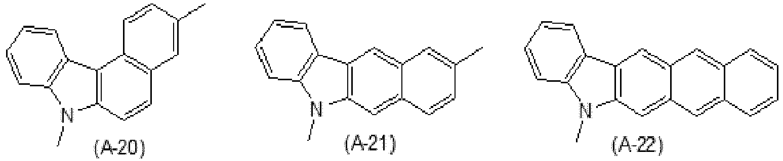
- As the photosensitization compound, a compound represented by the following Formula (6) is more preferably used.
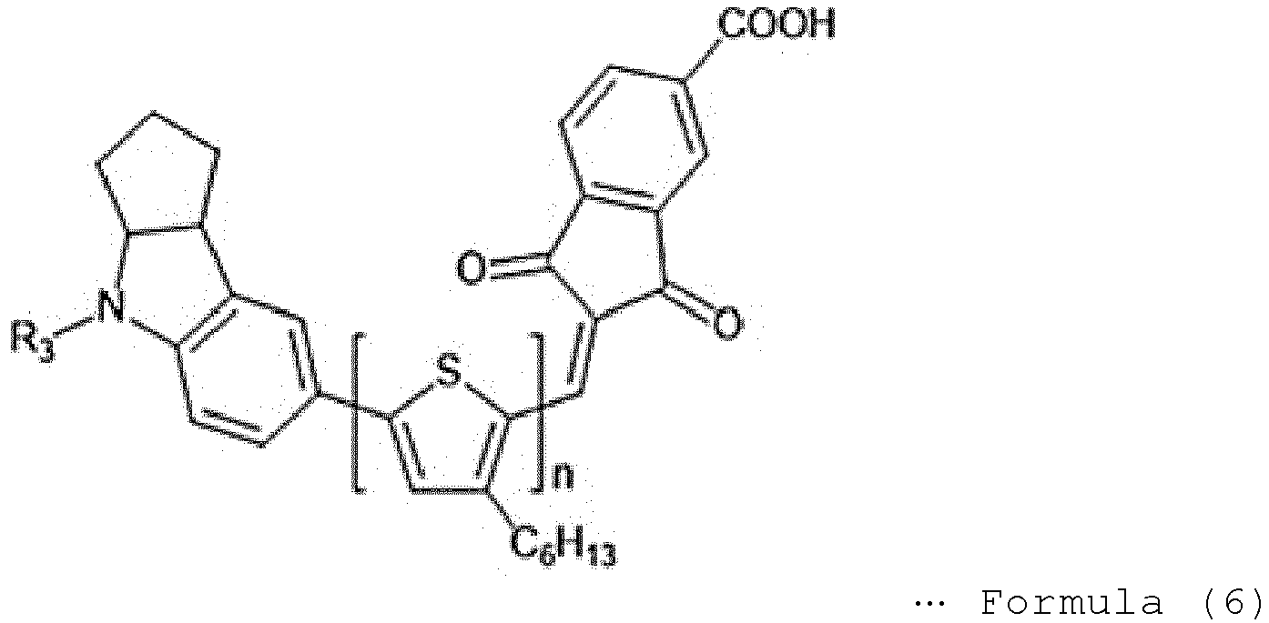
- In Formula (6), n represents an integer of 0 or 1, and R3 represent an aryl group that may have a substituent or one substituent selected from substituents expressed by the following three Structural Formulas.

- Specific examples of photosensitization compounds including Formula (5) and Formula (6) described above include the following (B-1) to (B-41), but are not limited thereto.


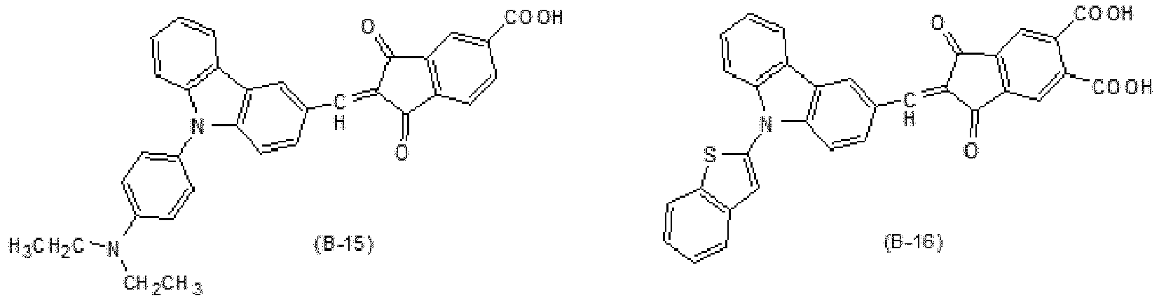


- Moreover, examples of preferably used photosensitization compounds also include compounds including the following Formula (7).

- In Formula (7), Ar1 and Ar2 represent an aryl group that may have a substituent. In Formula (7), R1 and R2 represent a straight-chain or branched alkyl group having from 4 through 10 carbon atoms. In Formula (7), X represents a substituent expressed by any one of the following Structural Formulas.

- Among the photosensitization compounds represented by the above Formula (7), a compound represented by the following Formula (8) is more preferably used.

- In Formula (8), Ar4 and Ar5 represent a phenyl group that may have a substituent or a naphthyl group that may have a substituent. In Formula (8), Ar6 represents a phenyl group that may have a substituent or a thiophene group that may have a substituent.
- As specific examples, exemplified compounds (B-42) to (B-58) of the photosensitization compounds represented by the above Formula (7) and the above Formula (8) are presented below, but the photosensitization compounds in the present disclosure are not limited thereto.


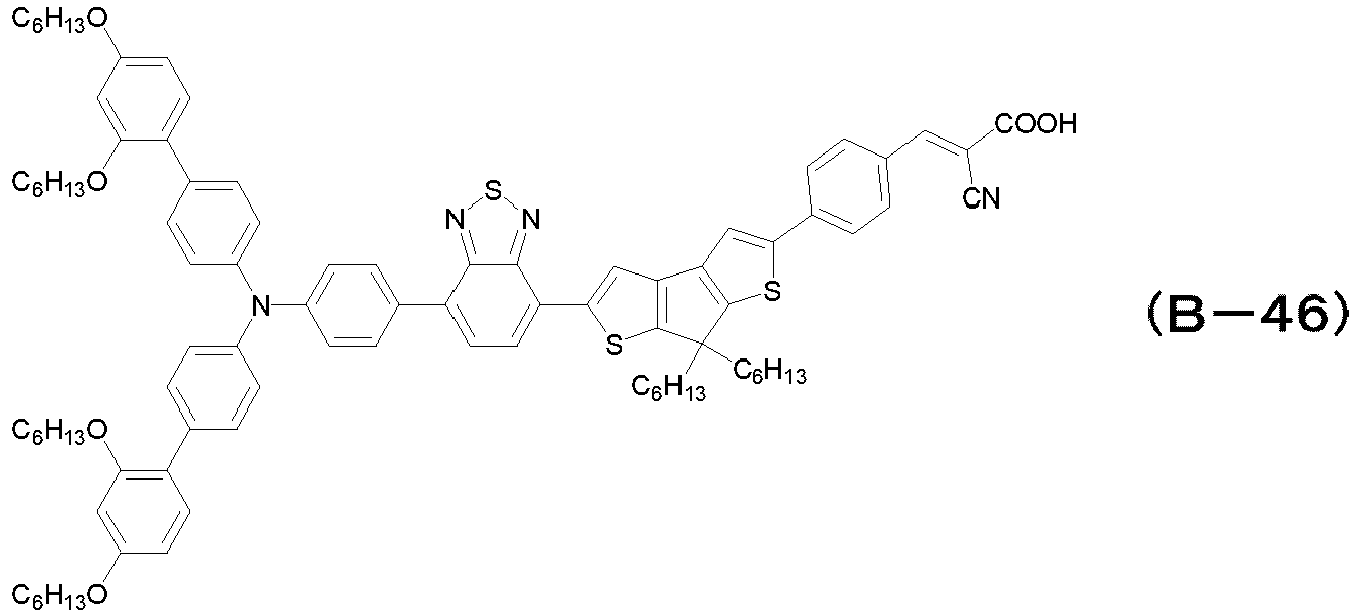


- In Formula (9), Ar7 and Are represent a phenyl group that may have a substituent or a naphthyl group that may have a substituent. In Formula (9), Ar9 represents a phenyl group that may have a substituent or a thiophene group that may have a substituent.
- Specific examples of the photosensitization compound represented by Formula (9) include exemplified compounds (B-59) to (B-62) as presented below, but the photosensitization compound of the present disclosure is not limited thereto.


- One kind of the photosensitization compound or two kinds or more of the photosensitization compounds may be included.
- A LED light source used as a light source has different colors such as warm colors, cold colors, or white color. The spectra differ depending on colors.
- For example, a color temperature of 3,000 K results in a relatively strong wavelength in a region of 600 nm, exhibiting a reddish light bulb color. Moreover, a color temperature of 5,000 K results in a well-balanced neutral white color as a whole. In addition, a color temperature of more than 6,500 K results in a relatively strong wavelength in a region of 450 nm, exhibiting a bluish daylight color.
- Therefore, the photoelectric conversion element can preferably maintain high output even when an LED having a different color temperature is used. In this case, inclusion of mixed photosensitization compounds different in absorption wavelength in the photoelectric conversion layer is effective because the output difference caused by color temperatures can be decreased.
- Examples of a method of adsorbing the photosensitization compound on the surface of the semiconductor material of the electron transport layer include: a method in which the electron transport layer including the semiconductor material is immersed in a solution of the photosensitization compound or a dispersion liquid of the photosensitization compound; and a method in which a solution of the photosensitization compound or a dispersion liquid of the photosensitization compound is coated and adsorbed on the electron transport layer.
- In the case of the method in which the electron transport layer including the semiconductor material is immersed in the solution of the photosensitization compound or the dispersion liquid of the photosensitization compound, for example, any of the following methods may be used: the immersion method, the dip method, the roller method, or the air knife method.
- In the case of the method in which the solution of the photosensitization compound or the dispersion liquid of the photosensitization compound is coated and adsorbed on the electron transport layer, for example, any of the following methods may be used: the wire bar method, the slide hopper method, the extrusion method, the curtain method, the spin method, or the spray method.
- The photosensitization compound can be adsorbed in a supercritical fluid including carbon dioxide.
- When the photosensitization compound is adsorbed on the semiconductor material, a condensation agent may be used in combination.
- The condensation agent may be a substance exhibiting a catalytic action that physically or chemically binds the photosensitization compound on the surface of the semiconductor material, or may be a substance that acts stoichiometrically and advantageously transfers chemical equilibrium. As an auxiliary condensation agent, thiol or a hydroxy compound may be added.
- Examples of solvents that dissolve or disperse the photosensitization compound include water, alcohol solvents, ketone solvents, ester solvents, ether solvents, amide solvents, halogenated hydrocarbon solvents, hydrocarbon solvents, and other solvents.
- Examples of the alcohol solvent include methanol, ethanol, isopropyl alcohol, and t-butanol.
- Examples of the ketone solvent include acetone, methyl ethyl ketone, and methyl isobutyl ketone.
- Examples of the ester solvent include ethyl formate, ethyl acetate, and n-butyl acetate.
- Examples of the ether solvent include diethyl ether, dimethoxy ethane, tetrahydrofuran, dioxolane, and dioxane.
- Examples of the amide solvent include N,N-dimethylformamide, N,N-dimethylacetoamide, and N-methyl-2-pyrrolidone.
- Examples of the halogenated hydrocarbon solvent include dichloromethane, chloroform, bromoform, methyl iodide, dichloroethane, trichloroethane, trichloroethylene, chlorobenzene, o-dichlorobenzene, fluorobenzene, bromobenzene, iodobenzene, and 1-chloronaphthalene.
- Examples of the hydrocarbon solvent include n-pentane, n-hexane, n-octane, 1,5-hexadiene, cyclohexane, methylcyclohexane, cyclohexadiene, benzene, toluene, o-xylene, m-xylene, p-xylene, ethylbenzene, and cumene.
- Examples of the other solvents include acetonitrile.
- These may be used alone or in combination.
- The photosensitization compound may work more effectively depending on its kind when aggregation between the compounds is minimized. Therefore, an aggregation dissociation agent may be used in combination.
- The aggregation dissociation agent is not particularly limited and may be appropriately selected in accordance with a dye to be used. Preferable examples thereof include steroid compounds such as cholic acid and chenodeoxycholic acid, long chain alkylcarboxylic acid, and long chain alkylphosphonic acid.
- The amount of the aggregation dissociation agent is preferably 0.01 parts by mass or more and 500 parts by mass or less, and more preferably 0.1 parts by mass or more and 100 parts by mass or less, relative to 1 part by mass of the photosensitization compound.
- When the photosensitization compound, or the photosensitization compound and the aggregation dissociation agent are adsorbed on the surface of the semiconductor material constituting the electron transport layer, its temperature is preferably -50°C or more and 200°C or less. The adsorption time is preferably 5 seconds or more and 1,000 hours or less, more preferably 10 seconds or more and 500 hours or less, and still more preferably 1 minute or more and 150 hours or less. The adsorption step is preferably performed in a dark place. The adsorption step may be performed statically or under stirring.
- The stirring method is not particularly limited and may be appropriately selected in accordance with the intended purpose. The method is, for example, a method using, for example, a stirrer, a ball mill, a paint conditioner, a sand mill, an attritor, a disperser, or ultrasonic dispersion.
- The electron transport layer preferably includes a perovskite layer adjacent to the electron transport layer and a bulk heterojunction layer.
- The perovskite layer means a layer that contains a perovskite compound and absorbs light to sensitize the electron transport layer. Therefore, the perovskite layer is preferably disposed adjacent to the electron transport layer.
- The shape and size of the perovskite layer are not particularly limited and may be appropriately selected in accordance with the intended purpose.
- The perovskite compound is a complex substance of an organic compound and an inorganic compound, and is represented by the following Formula (X).
XαYβZγ··· Formula (X)
- In Formula (X), a ratio of (α:β:γ is 3:1:1; β and γ are each an integer of more than 1; X represents halogen; Y represents an organic compound including an amino group; and Z represents a metal ion.
- X in Formula (X) is not particularly limited and may be appropriately selected in accordance with the intended purpose. Examples thereof include halogen such as chlorine, bromine, and iodine. These may be used alone or in combination.
- Y in the above Formula (X) is not particularly limited and may be appropriately selected in accordance with the intended purpose as long as it is an organic cation. Examples thereof include: ions of alkyl amine compounds (e.g., methyl amine, ethyl amine, n-butylamine, and formamidine); and inorganic alkali metal cations (e.g., antimony ions, cesium ions, potassium ions, and rubidium ions). These may be used alone or in combination. The inorganic alkali metal cation and the organic cation may be each used in combination. Among them, an organic compound including an amino group (an ion of an alkyl amine compound) is preferable.
- In the case of the perovskite compound of lead halide and methylammonium, a peak λmax of the optical absorption spectrum is about 350 nm when the halogen ion is Cl, the peak λmax is about 410 nm when the halogen ion is Br, and the peak λmax is about 540 nm when the halogen ion is I. As described above, the peak λmax is shifted to a longer wavelength side, so a usable spectrum width (band width) varies.
- Z in the above Formula (X) is not particularly limited and may be appropriately selected in accordance with the intended purpose. Examples thereof include ions of metals such as lead, indium, antimony, tin, copper, and bismuth. These may be used alone or in combination.
- The perovskite layer preferably has a stacked perovskite structure where a layer formed of metal halide and a layer of arranged organic cation molecules are stacked on top of one another.
- An average film thickness of the perovskite layer is 50 nm or more and 2 µm or less, and more preferably 100 nm or more and 600 nm or less.
- A method of forming the perovskite layer is not particularly limited and may be appropriately selected in accordance with the intended purpose. Examples of the method include a method in which a solution obtained by dissolving or dispersing, for example, metal halide and halogenated alkylamine or cesium halide is coated, followed by drying.
- Moreover, examples of the method of forming the perovskite layer include a two-step precipitation method as described below. Specifically, for example, a solution obtained by dissolving or dispersing metal halide is coated, followed by drying. Then, the dried product is immersed in a solution obtained by dissolving halogenated alkylamine, to form the perovskite compound.
- Moreover, examples of the method of forming the perovskite layer include a method in which a poor solvent (solvent having a small solubility) for the perovskite compound is added while a solution obtained by dissolving or dispersing, for example, metal halide and halogenated alkylamine is coated thereon, to precipitate crystals.
- In addition, examples of the method of forming the perovskite layer include a method in which metal halide is deposited in a gas filled with, for example, methylamine.
- Among them, it is preferable to use a method in which a poor solvent for the perovskite compound is added while a solution obtained by dissolving or dispersing, for example, metal halide and halogenated alkylamine is coated thereon, to precipitate crystals.
- A method of coating the solution is not particularly limited and may be appropriately selected in accordance with the intended purpose. Examples of the method include the immersion method, the spin coating method, the spray method, the dip method, the roller method, and the air knife method. As the method of coating the solution, a method of performing precipitation in a supercritical fluid using, for example, carbon dioxide may be used.
- The perovskite layer may include a photosensitization dye (photosensitization compound).
- A method of forming the perovskite layer including the photosensitization dye (photosensitization compound) is not particularly limited and may be appropriately selected in accordance with the intended purpose. Examples of the method include: a method in which the perovskite compound and the photosensitization dye (photosensitization compound) are mixed; and a method in which the perovskite layer is formed, followed by adsorbing the photosensitization dye (photosensitization compound).
- The photosensitization dye (photosensitization compound) is not particularly limited and may be appropriately selected in accordance with the intended purpose, as long as it is a compound photoexcited by excitation light to be used.
- Examples of photosensitization dyes (photosensitization compound) include metal complex compounds, coumarin compounds, polyene compounds, indoline compounds, thiophene compounds, cyanine dyes, merocyanine dyes, 9-aryl xanthene compounds, triarylmethane compounds, phthalocyanine compounds, and porphyrin compounds.
- Examples of metal complex compounds include metal complex compounds described in, for example,
Japanese Translation of PCT International Application Publication No. 7-500630 Japanese Unexamined Patent Application Publication No. 10-233238 Japanese Unexamined Patent Application Publication No. 2000-26487 Japanese Unexamined Patent Application Publication No. 2000-323191 Japanese Unexamined Patent Application Publication No. 2001-59062 - Examples of coumarin compounds include coumarin compounds described in, for example,
Japanese Unexamined Patent Application Publication No. 10-93118 Japanese Unexamined Patent Application Publication No. 2002-164089 Japanese Unexamined Patent Application Publication No. 2004-95450 - Examples of polyene compounds include polyene compounds described in, for example,
Japanese Unexamined Patent Application Publication No. 2004-95450 - Examples of indoline compounds include indoline compounds described in, for example,
Japanese Unexamined Patent Application Publication No. 2003-264010 Japanese Unexamined Patent Application Publication No. 2004-63274 Japanese Unexamined Patent Application Publication No. 2004-115636 Japanese Unexamined Patent Application Publication No. 2004-200068 Japanese Unexamined Patent Application Publication No. 2004-235052 - Examples of thiophene compounds include thiophene compounds described in, for example, J. Am. Chem. Soc., 16701, Vol. 128 (2006) and J. Am. Chem. Soc., 14256, Vol. 128 (2006).
- Examples of cyanine dyes include cyanine dyes described in, for example,
Japanese Unexamined Patent Application Publication No. 11-86916 Japanese Unexamined Patent Application Publication No. 11-214730 Japanese Unexamined Patent Application Publication No. 2000-106224 Japanese Unexamined Patent Application Publication No. 2001-76773 Japanese Unexamined Patent Application Publication No. 2003-7359 - Examples of merocyanine dyes include merocyanine dyes described in, for example,
Japanese Unexamined Patent Application Publication No. 11-214731 Japanese Unexamined Patent Application Publication No. 11-238905 Japanese Unexamined Patent Application Publication No. 2001-52766 Japanese Unexamined Patent Application Publication No. 2001-76775 Japanese Unexamined Patent Application Publication No. 2003-7360 - Examples of 9-aryl xanthene compounds include 9-aryl xanthene compounds described in, for example,
Japanese Unexamined Patent Application Publication No. 10-92477 Japanese Unexamined Patent Application Publication No. 11-273754 Japanese Unexamined Patent Application Publication No. 11-273755 Japanese Unexamined Patent Application Publication No. 2003-31273 - Examples of triarylmethane compounds include triarylmethane compounds described in, for example,
Japanese Unexamined Patent Application Publication No. 10-93118 Japanese Unexamined Patent Application Publication No. 2003-31273 - Examples of phthalocyanine compounds and porphyrin compounds include phthalocyanine compounds and porphyrin compounds described in, for example,
Japanese Unexamined Patent Application Publication No. 9-199744 Japanese Unexamined Patent Application Publication No. 10-233238 Japanese Unexamined Patent Application Publication No. 11-204821 Japanese Unexamined Patent Application Publication No. 11-265738 Japanese Unexamined Patent Application Publication No. 2006-032260 - Among them, metal complex compounds, indoline compounds, thiophene compounds, and porphyrin compounds are preferable.
- The bulk heterojunction layer includes an electron-donating organic material and an electron-withdrawing organic material.
- In the bulk heterojunction layer, the electron-donating organic material (P-type organic semiconductor) and the electron-withdrawing organic material (N-type organic semiconductor) are mixed, and thus the bulk heterojunction, which is the nano-sized PN junction, will occur. As a result, photocharge separation occurring at the junction surface can be used to obtain electric current.
- Examples of the P-type organic semiconductor include conjugated polymers and low-molecular-weight compounds such as polythiophene or derivatives thereof, arylamine derivatives, stilbene derivatives, oligothiophene or derivatives thereof, phthalocyanine derivatives, porphyrin or derivatives thereof, polyphenylene vinylene or derivatives thereof, polythienylene vinylene or derivatives thereof, benzodithiophene derivatives, and diketo-pyrrolo-pyrrole derivatives. These may be used alone or in combination.
- Among the above, polythiophene or derivatives thereof, which are n-conjugated conductive polymers, are preferable. The polythiophene and derivatives thereof are advantageous because they can ensure an excellent stereoregularity and have a relatively high solubility to a solvent.
- The polythiophene and the derivatives thereof are not particularly limited and may be appropriately selected in accordance with the intended purpose, as long as they have a thiophene skeleton. Examples thereof include: polyalkylthiophene such as poly-3-hexylthiophene; polyalkylisothionaphthene such as poly-3-hexylisothionaphthene, poly-3-octylisothionaphthene, and poly-3-decylisothionaphthene; and polyethylenedioxythiophene.
- In recent years, derivatives such as PTB7 (poly[{4,8-bis[(2-ethylhexyl)oxy]benzo[1,2-b:4,5-b']dithiophene-2,6-diyl}{3-fluoro-2-[(2-ethylhexyl)carbonyl]thieno[3,4-b]thiophenediyl}]) and PCDTBT (poly[N-9"-heptadecanyl-2,7-carbazole-alt-5,5-(4',7'-di-2-thienyl-2',1',3'-benzothiadiazole])), which are copolymers including benzodithiophene, carbazole, benzothiadiazole, and thiophene, have been exemplified as compounds that can achieve an excellent photoelectric conversion efficiency.
- In addition to the conjugated polymers, even in the low-molecular-weight compounds obtained by binding an electron-donating unit with an electron-withdrawing unit, compounds that can achieve an excellent photoelectric conversion efficiency have been known and can also be used in the present disclosure (see, for example, ACSAppl. Mater. ).
- Among the low-molecular-weight compounds as the electron-donating organic material, a compound represented by the following Formula (A) is preferable.

- In Formula (A), n represents an integer of from 1 through 3.
- In Formula (A), R1 represents an n-butyl group, an n-hexyl group, an n-octyl group, an n-decyl group, or an n-dodecyl group.
- In Formula (A), R2 represents an oxygen atom that has an alkyl group having from 6 through 22 carbon atoms, a sulfur atom that has an alkyl group having from 6 through 22 carbon atoms, a carbon atom that has an alkyl group having from 6 through 22 carbon atoms, or a group represented by the following Formula (B). Among them, an oxygen atom that has an alkyl group having from 6 through 20 carbon atoms, a sulfur atom that has an alkyl group having from 6 through 20 carbon atoms, a carbon atom that has an alkyl group having from 6 through 20 carbon atoms, and a group represented by the following Formula (B) are preferable.

- In Formula (B), R3 and R4 represent a hydrogen atom or an alkyl group having from 6 through 12 carbon atoms.
- In Formula (B), R5 represents an alkyl group that may include a branched chain having from 6 through 22 carbon atoms. Among them, an alkyl group that may include a branched chain having from 6 through 12 carbon atoms is preferable.
- More specific examples of the low-molecular-weight compound as the electron-donating organic material are preferably compounds represented by the following Formula (C).

- In Formula (C), R3 and R4 represent a hydrogen atom or an alkyl group having from 6 through 12 carbon atoms, and preferably represent a hydrogen atom or an alkyl group having from 6 through 10 carbon atoms.
- In Formula (C), R5 represents an alkyl group that may include a branched chain having from 6 through 22 carbon atoms, and preferably represents an alkyl group that may include a branched chain having from 6 through 12 carbon atoms.
- Specific examples of the compound represented by Formula (C) will be described below. However, the present disclosure is not limited thereto.
Table 1 Exemplified compounds R3 R4 R5 1 H H 2-ethylhexyl 2 H n-hexyl n-hexyl 3 H H n-hexyl 4 n-hexyl H n-hexyl 5 H H 2-butyl octyl 6 H n-octyl n-octyl 7 H H n-octyl 8 n-octyl H n-octyl 9 H H 2-decyldodecyl 10 H n-dodecyl n-dodecyl 11 H H n-dodecyl 12 n-dodecyl H n-dodecyl - Examples of the electron-withdrawing organic material include imide derivatives, fullerene, and fullerene derivatives. Among them, fullerene derivatives are preferable in terms of charge separation and charge transport.
- As the fullerene derivative, an appropriately synthesized product may be used or a commercially available product may be used. Examples thereof include product names of PC71BM (phenyl C71 butyric acid methyl ester, manufactured by Frontier Carbon Corporation), PC61BM (phenyl C61 butyric acid methyl ester, manufactured by Frontier Carbon Corporation), PC85BM (phenyl C85 butyric acid methyl ester, manufactured by Frontier Carbon Corporation), and ICBA (
fullerene indene 2 adduct, manufactured by Frontier Carbon Corporation). In addition to the above, fulleropyrrolidine-based fullerene derivatives represented by the following Formula (D) may be used.
- In Formula (D), Y1 and Y2, which may be identical to or different from each other, represent a hydrogen atom, an alkyl group that may have a substituent, an alkenyl group that may have a substituent, an alkynyl group that may have a substituent, an aryl group that may have a substituent, or an aralkyl group that may have a substituent.
- Note that, in Formula (D), Y1 and Y2 are not a hydrogen atom at the same time.
- In Formula (D), the Ar represents an aryl group that may have a substituent.
- Specific examples of the aryl group include a phenyl group, a naphthyl group, an anthryl group, and a phenanthryl group. Among them, a phenyl group is preferable.
- In Formula (D), as the substituent in the aryl group that has a substituent represented by the Ar, the substituent preferably excludes an oxygen atom. Examples of the substituent in the aryl group that has the substituent represented by the Ar include an aryl group, an alkyl group, a cyano group, an alkoxy group, and an alkoxycarbonyl group. Among these substituents, examples of the aryl group include a phenyl group.
- The alkyl group and the alkyl group portion of the alkoxy group are, for example, an alkyl group having from 1 through 22 carbon atoms similarly with alkyl groups represented by Y1 and Y2 that will be described below.
- The number and substitution site of these substituents are not particularly limited. For example, one to three substituent(s) can exist at any position of the aryl group represented by Ar.
- In Formula (D), among the groups represented by the Y1 and the Y2, the alkyl group is preferably an alkyl group having from 1 through 22 carbon atoms, more preferably an alkyl group having from 1 through 12 carbon atoms, and particularly preferably an alkyl group having from 6 through 12 carbon atoms. These alkyl groups may be a straight-chain alkyl group or may be a branched alkyl group, but are particularly preferably a straight-chain alkyl group.
- The alkyl group may further include one or two or more hetero elements such as S and O in the carbon chain thereof.
- In Formula (D), among the groups represented by the Y1 and the Y2, the alkenyl group is preferably an alkenyl group having from 2 through 10 carbon atoms. More preferable specific examples thereof include straight-chain or branched alkenyl groups having from 2 through 4 carbon atoms such as a vinyl group, a 1-propenyl group, an allyl group, an isopropenyl group, a 1-butenyl group, a 2-butenyl group, a 3-butenyl group, a 1-methyl-2-propenyl group, and a 1,3-butadienyl group.
- In Formula (D), among the groups represented by the Y1 and the Y2, the alkynyl group is preferably an alkynyl group having from 1 through 10 carbon atoms. More preferable specific examples thereof include straight-chain or branched alkynyl groups having from 2 through 4 carbon atoms such as an ethynyl group, a 1-propynyl group, a 2-propynyl group, a 1-methyl-2-propynyl group, a 1-butynyl group, a 2-butynyl group, and a 3-butynyl group.
- In Formula (D), among the groups represented by the Y1 and the Y2, examples of the aryl group include a phenyl group, a naphthyl group, an anthryl group, and a phenanthryl group.
- In Formula (D), among the groups represented by the Y1 and the Y2, examples of the aralkyl group include aralkyl groups having from 7 through 20 carbon atoms such as 2-phenylethyl, benzyl, 1-phenylethyl, 3-phenylpropyl, and 4-phenylbutyl.
- As described above, in Formula (D), the alkyl group, the alkenyl group, the alkynyl group, the aryl group, and the aralkyl group of the groups represented by the Y1 and the Y2 include a case of including a substituent and a case of including no substituent.
- In Formula (D), examples of the substituents that can be included in the groups represented by the Y1 and the Y2 include an alkyl group, an alkoxycarbonyl group, a polyether group, an alkanoyl group, an amino group, an aminocarbonyl group, an alkoxy group, an alkylthio group, a group: -CONHCOR' (wherein R' is an alkyl group), a group: -C(=NR')-R" (wherein R' and R" are an alkyl group), and a group: -NR'=CRʺR‴ (wherein R', R", and R‴ are an alkyl group).
- In Formula (D), among the substituents that can be included in the groups represented by the Y1 and the Y2, examples of the polyether group include a group represented by the formula: Y3-(OY4)n-O-. Here, Y3 represents a monovalent hydrocarbon group such as an alkyl group, and Y4 represents a bivalent aliphatic hydrocarbon group.
- In the polyether group represented by the above formula, specific examples of recurring units represented by - (OY4)n- include alkoxy chains such as -(OCH2)n-, -(OC2H4)n-, and - (OC3H6)n-. The recurring number n of these recurring units is preferably from 1 through 20, and more preferably from 1 through 5. The recurring unit represented by -(OY4)n- may include not only the same recurring unit but also two or more kinds of different recurring units. Among the aforementioned recurring units, -OC2H4- and -OC3H6- may have a straight chain or a branched chain.
- In Formula (D), among the substituents that can be included in the groups represented by the Y1 and the Y2, the alkyl group portion (R', R") in the alkoxycarbonyl group, the alkanoyl group, the alkoxy group, the alkylthio group, the polyether group, the group: -CONHCOR', the group: -C(=NR')-R", and the group: -NR'=CRʺR‴ are preferably an alkyl group having from 1 through 22 carbon atoms, more preferably an alkyl group having from 1 through 12 carbon atoms, and particularly preferably an alkyl group having from 6 through 12 carbon atoms, similarly with the aforementioned alkyl group.
- The amino group, and the amino group portion in the aminocarbonyl group are particularly preferably an amino group to which one or more alkyl groups having from 1 through 20 carbon atoms are bound.
- Among the fullerene derivatives represented by the Formula (D), examples of the compound having preferable performances include compounds represented by the Formula (D), where, in the Formula (D), Ar represents a phenyl group that has a substituent or a phenyl group that has no substituent; and one of Y1 and Y2 is a hydrogen atom, and the other is an alkyl group including an alkoxycarbonyl group as a substituent, an alkyl group including an alkoxy group as a substituent, an alkyl group including a polyether group as a substituent, an alkyl group including an amino group as a substituent, or a phenyl group that includes a substituent or includes no substituent.
- Among such compounds, examples of the compound having particularly preferable performances include compounds represented by Formula (D), where Ar is a phenyl group that includes, as a substituent, a phenyl group, a cyano group, an alkoxy group, an alkoxycarbonyl group, or an alkyl group, or is a phenyl group without a substituent; and one of Y1 and Y2 is a hydrogen atom, and the other is an alkyl group including an alkoxycarbonyl group as a substituent, an alkyl group including an alkoxy group as a substituent, an alkyl group including a polyether group as a substituent, a phenyl group, a phenyl group including an alkyl group as a substituent, a phenyl group including an alkoxycarbonyl group as a substituent, or a phenyl group including an alkoxycarbonyl group as a substituent.
- These compounds include a group having an appropriate polarity on the pyrrolidine skeleton and are excellent in a selfassembling property. Therefore, when a photoelectric conversion layer having a bulk heterojunction structure is formed, it is possible to form a photoelectric conversion part that has a bulk heterojunction structure having an appropriate layer separation structure. As a result, it is believed that, for example, the electron mobility is improved to exhibit a high conversion efficiency.
- Examples of the most preferable compound include compounds represented by Formula (D), where Ar is a phenyl group; one of Y1 and Y2 represents a hydrogen atom, and the other represents a non-substituted alkyl group (alkyl group having from 4 through 6 carbon atoms), a non-substituted phenyl group, a 1-naphthyl group, or a 2-naphthyl group.
- The method of forming the bulk heterojunction layer is not particularly limited and may be appropriately selected in accordance with the intended purpose. Examples of the method include spin coating, blade coating, slit die coating, screenprint coating, bar coater coating, mold coating, transfer printing method, dip drawing method, the inkjet method, the spray method, and vacuum deposition method. The method can be appropriately selected from the above depending on the characteristics (e.g., thickness control and orientation control) of the thin film of the organic material to be produced.
- In order to remove an organic solvent from the produced thin film of the organic material, an annealing treatment may be performed under reduced pressure or under an inert atmosphere (under nitrogen or argon atmosphere). The temperature of the annealing treatment is preferably 40°C or more and 300°C or less, and more preferably 50°C or more and 200°C or less. The annealing treatment can increase an effective area where stacked layers permeate at the boundary to contact each other. Therefore, the short circuit current can be increased. Note that, the annealing treatment may be performed after formation of electrodes.
- The organic solvent is not particularly limited and may be appropriately selected in accordance with the intended purpose. Examples of the solvent include methanol, ethanol, butanol, toluene, xylene, o-chlorophenol, acetone, ethyl acetate, ethylene glycol, tetrahydrofuran, dichloromethane, chloroform, dichloroethane, chlorobenzene, dichlorobenzene, trichlorobenzene, chloronaphthalene, dimethylformamide, dimethyl sulfoxide, N-methylpyrrolidone, and γ-butyrolactone. These may be used alone or in combination. Among them, chlorobenzene, chloroform, and o-dichlorobenzene are preferable.
- In order to control the phase separation structure of the P-type organic semiconductor and the N-type organic semiconductor, an additive may be added to the organic solvent in an amount of 0.1% by mass or more and 10% by mass or less. Examples of the additive include diiodoalkanes (e.g., 1,8-diiodooctane, 1,6-diiodohexane, and 1,10-diiododecane), alkane dithiols (e.g., 1,8-octanedithiol, 1,6-hexanedithiol, and 1,10-decanedithiol), 1-chloronaphthalene, and polydimethylsiloxane derivatives.
- The average thickness of the photoelectric conversion layer is preferably 50 nm or more and 400 nm or less, and more preferably 60 nm or more and 250 nm or less. When the average thickness of the photoelectric conversion layer is 50 nm or more, insufficient generation of carriers, which is caused by decreasing light absorption in the photoelectric conversion layer, does not occur. When the average thickness is 400 nm or less, the transport efficiency of carriers generated by light absorption is not further decreased.
- The photoelectric conversion element preferably includes a hole transport layer.
- The hole transport layer is a layer that transports holes and includes a basic compound. The hole transport layer preferably includes a hole transport material and an alkali metal salt, and may further include other materials if necessary.
- The basic compound preferably has an acid dissociation constant (pKa) of 6 or more and 10 or less. Examples of the basic compound having the aforementioned range of the acid dissociation constant (pKa) include pyridine compounds and imidazole compounds. Among them, pyridine compounds are preferable.
- The pyridine compound is a compound represented by at least one selected from the following Formula (10) and the following Formula (11).


- In Formula (10) and Formula (11), Ar1 and Ar2 represent an aryl group that may have a substituent, and the Ar1 and the Ar2, which may be identical to or different from each other, may be bound to each other.
- Specific examples of the aryl group include phenyl groups, naphthyl groups, and biphenyl groups. Examples of the substituent include alkyl groups and alkoxy groups.
- Hereinafter, specific exemplified compounds (H-1) to (H-8) of the pyridine compounds represented by Formula (10) are presented, but the pyridine compounds in the present disclosure are not limited thereto.


- The amount of the above pyridine compound in the hole transport layer is preferably 20 mol% or more and 65 mol% or less, and more preferably 35 mol% or more and 50 mol% or less, relative to the hole transport material. When the amount of the pyridine compound satisfies the preferable range, high open circuit voltage can be maintained, high output can be obtained, and high stability and durability can be obtained even after long-term use under various conditions (particularly, low temperature environment).
- In order to obtain the function of transporting holes, the hole transport layer preferably includes, for example, a hole transport material or a p-type semiconductor material as a hole transport material.
- As the hole transport material or the p-type semiconductor material, a conventional organic hole transport compound can be used.
- Specific examples of the organic hole transport compound include oxadiazole compounds, triphenylmethane compounds, pyrazoline compounds, hydrazone compounds, oxadiazole compounds, tetraarylbenzidine compounds, stilbene compounds, and spiro-type compounds. Among them, spiro-type compounds are more preferable.
- The spiro-type compound is preferably a compound including the following Formula (12).

- Note that, in Formula (12), R31 to R34 each independently represent a substituted amino group such as a dimethylamino group, a diphenylamino group, or a naphthyl-4-tolylamino group.
- Specific examples of the spiro-type compound include the following (D-1) to (D-20), but are not limited thereto.
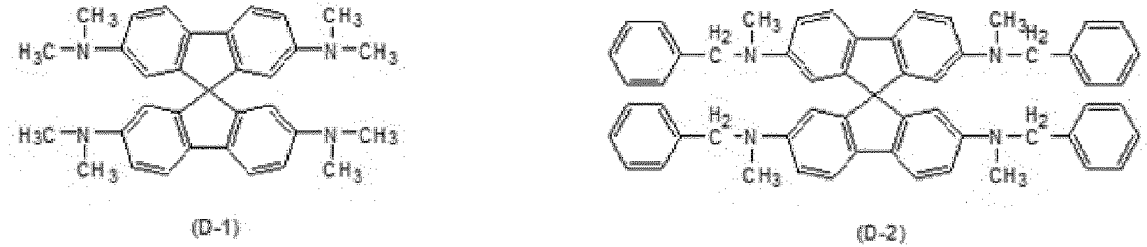


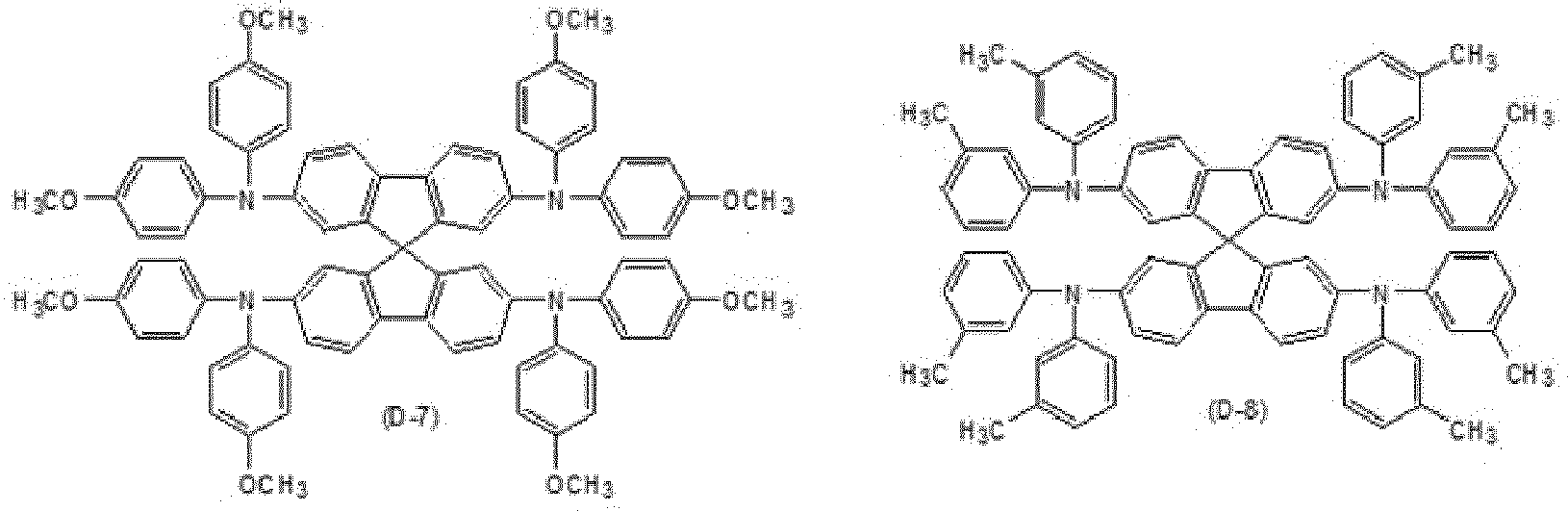


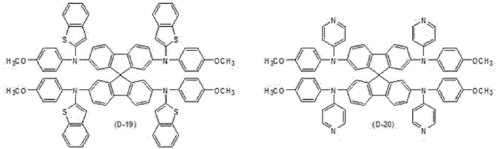
- As the spiro-type compound as the hole transport material, a compound represented by the following Formula (13) is particularly suitably used.

- In Formula (13), R3 represents a hydrogen atom or an alkyl group.
- For example, among the above (D-1) to (D-20), those represented by the above Formula (13) are (D-7) and (D-10).
- These spiro-type compounds have a high hole mobility. In addition, the spiro-type compounds exhibit excellent a photoelectric conversion characteristic because two benzidine skeleton molecules are bound with being twisted to thereby form almost spherical electron cloud, and intermolecular hopping conductivity is good. Moreover, the spiro-type compounds are dissolved in various organic solvents because of high solubility, and are easily densely filled in the porous electron transport layer because of its amorphous property (amorphous substance having no crystal structure). The spiro-type compounds allow the photosensitization compound to efficiently absorb light because they have no light absorption characteristics of 450 nm or more. Therefore, such spiro-type compounds are particularly preferable for solid-type dye sensitized solar cells.
- Examples of the alkali metal salt include lithium salts, sodium salts, and potassium salts.
- Examples of the lithium salt include lithium chloride, lithium bromide, lithium iodide, lithium perchlorate, lithium bis(trifluoromethanesulfonyl)diimide, lithium diisopropylimide, lithium acetate, lithium tetrafluoroborate, lithium pentafluorophosphate, and lithium tetracyanoborate.
- Examples of the sodium salt include sodium chloride, sodium bromide, sodium iodide, sodium perchlorate, sodium bis(trifluoromethanesulfonyl)diimide, sodium acetate, sodium tetrafluoroborate, sodium pentafluorophosphate, and sodium tetracyanoborate.
- Examples of the potassium salt include potassium chloride, potassium bromide, potassium iodide, and potassium perchlorate.
- Among them, lithium salt is preferable, and lithium bis(trifluoromethanesulfonyl)diimide and lithium diisopropylimide are more preferable because electric conductivity can be improved and the durability and the stability of output characteristics can be improved.
- The lithium salt is preferably a compound represented by the following Formula (14).

- In Formula (14), A and B represent any one of substituents F, CF3, C2F5, C3F7, and C4F9. The substituent A and the substituent B are preferably different from each other.
- Examples of the lithium salt include lithium (fluorosulfonyl)(trifluoromethanesulfonyl)imide (Li-FTFSI), lithium (fluorosulfonyl)(pentafluoroethanesulfonyl)imide (Li-FPFSI), lithium (fluorosulfonyl)(nonafluorobutanesulfonyl)imide (Li-FNFSI), lithium (nonafluorobutanesulfonyl)(trifluoromethanesulfonyl)imide (Li-NFTFSI), and lithium (pentafluoroethanesulfonyl)(trifluoromethanesulfonyl)imide (Li-PFTFSI). Among them, lithium (fluorosulfonyl)(trifluoromethylsulfonyl)imide (Li-FTFSI) is preferable.
- The Structural Formulas of the specific examples of the lithium salts are, for example, as follows.


- Here, when a coating liquid for forming the hole transport layer that includes the lithium salt is coated, the above lithium salt does not need to be contained in the formed film in a salt state where a cation and an anion are bound to each other, and may be included in the state where a cation and an anion are separated. Specifically, the present inventors found that when the hole transport layer is formed with the lithium salt being included in the coating liquid for the hole transport layer, lithium cations migrate to the electron transport layer, and therefore the electron transport layer includes more lithium cations than the hole transport layer. On the other hand, the present inventors found that anions partially migrate to the electron transport layer, but the hole transport layer includes more anions than the electron transport layer.
- Preferably, in the present disclosure, cations and anions of the lithium salt are separated, and each have a different distribution state. When they are included in the photoelectric conversion layer, high output can be obtained with light having a low illuminance under low temperature environments and the effect such as excellent persistence of the output can be further improved.
- The hole transport layer in the photoelectric conversion layer may include a lithium salt having another structure in addition to the lithium salt represented by the above Formula (14). Examples of the lithium salts include, in addition to the aforementioned lithium salts, lithium salts having symmetric anion species. Specific examples thereof include: lithium bis(fluorosulfonyl)imide (Li-FSI), lithium bis(trifluoromethanesulfonyl)imide (Li-TFSI), lithium bis(pentafluoroethanesulfonyl)imide (Li-BETI), and lithium bis(nonafluorobutanesulfonyl)imide; and cyclic imides such as lithium (cyclohexafluoropropane)(disulfone)imide.
- These lithium salts, however, have a low solubility because anions are symmetric. Therefore, its addition amount is not easily increased, and is preferably a small amount even when the lithium salt is added.
- An amount of the lithium salt represented by the above Formula (14) is preferably 5 mol% or more and 50 mol% or less, and more preferably 20 mol% or more and 35 mol% or less, relative to the hole transport material. When the amount of the lithium salt represented by the above Formula (14) falls within the aforementioned range, a high output with respect to light having a low illuminance can be achieved, the maintenance rate of the output can be improved, and high durability can be achieved.
- In particular, a molar ratio (a/b) of the pyridine compound to the lithium salt in the photoelectric conversion layer is preferably less than 2.0, more preferably 1.8 or less, and still more preferably 1.7 or less, where the a is a molar amount of the pyridine compound in the photoelectric conversion layer and the b is an amount of the lithium salt in the photoelectric conversion layer.
- The molar ratio (a/b) of the pyridine compound to the lithium salt falling less than 2.0 is advantageous because high output can be maintained for longer period of time when light having a low illuminance is emitted under low temperature environments and the durability of the photoelectric conversion element can be further improved.
- In addition to the hole transport material or the lithium salt, an oxidizing agent is preferably added to the hole transport layer. Addition of the oxidizing agent improves the hole transport property and can enhance output characteristics or its durability or stability.
- Examples of the oxidizing agent include tris(4-bromophenyl) aminium hexachloroantimonate, silver hexafluoroantimonate, nitrosonium tetrafluoroborate, nitric acid silver, metal complexes, and hypervalent iodine compounds. Among them, metal complexes and hypervalent iodine compounds are suitably used.
- When the oxidizing agent is a metal complex or a hypervalent iodine compound, a large amount of the oxidizing agent can be added to the hole transport layer because of its high solubility in an organic solvent. As a result, the hole transport property is improved and the persistence of the hole transport property is excellent.
- The metal complex includes a metal cation, a ligand, and an anion.
- Examples of the metal cation include cations such as chromium, manganese, iron, cobalt, nickel, copper, molybdenum, ruthenium, rhodium, palladium, silver, tungsten, rhenium, osmium, iridium, gold, and platinum. Among them, a cation such as cobalt, iron, nickel, or copper is preferable, and a cobalt complex is more preferable.
- The ligand preferably includes a 5-membered and/or 6-membered heterocycle including at least one nitrogen, which may have a substituent. Specific examples thereof include the following (E-1) to (E-33) but are not limited thereto.





- Examples of the suitable anion include hydride ions (H-), fluoride ions (F-), chloride ions (Cl-), bromide ions (Br-), iodide ions (I-), hydroxide ions (OH-), cyanide ions (CN-), nitric acid ions (NO3 -), nitrous acid ions (NO2 -), hypochlorous acid ions (ClO-), chlorous acid ions (ClO2 -), chloric acid ions (ClO3 -), perchloric acid ions (ClO4 -), permanganic acid ions (MnO4 -), acetic acid ions (CH3COO-), hydrogen carbonate ions (HCO3 -), dihydrogen phosphate ions (H2PO4 -), hydrogen sulfate ions (HSO4 -), hydrogen sulfide ions (HS-), thiocyanic acid ions (SCN-), tetrafluoroboric acid ions (BF4 -), hexafluorophosphate ions (PF6 -), tetracyanoborate ions (B(CN)4 -), dicyanoamine ions (N(CN)2 -), p-toluenesulfonic acid ions (TsO-), trifluoromethyl sulfonate ions (CF3SO2 -), bis(trifluoromethylsulfonyl)amine ions (N(SO2CF3)2-), tetrahydroxoaluminate ions ([Al(OH)4]- or [Al(OH)4(H2O)2]-), dicyanoargentate(I) ions ([Ag(CN)2] -), tetrahydroxochromate(III) ions ([Cr(OH)4]-), tetrachloroaurate(III) ions ([AuCl4]-), oxide ions (O2-), sulfide ions (S2-), peroxide ions (O2 2-), sulfuric acid ions (SO4 2-), sulfurous acid ions (SO3 2-), thiosulfuric acid (S2O3 2-), carbonic acid ions (CO3 2-), chromic acid ions (CrO4 2-), dichromic acid ions (Cr2O7 2-), monohydrogen phosphate ions (HPO4 2-), tetrahydroxozincate(II) ions ([Zn(OH)4]2-), tetracyanozincate(II) ions ([Zn(CN)4]2-), tetrachlorocuprate(II) ions ([CuCl4]2-), phosphoric acid ions (PO4 3-), hexacyanoferrate(III) ions ([Fe(CN)6]3-), bis(thiosulfate)argentate(I) ions ([Ag(S2O3)2]3-), and hexacyanoferrate(II) ions ([Fe(CN)6]4-).
- These may be used alone or in combination.
- Among them, tetrafluoroboric acid ions, hexafluorophosphate ions, tetracyanoborate ions, bis(trifluoromethylsulfonyl)amine ions, and perchloric acid ions are preferable.
- Among these metal complexes, a trivalent cobalt complex is preferably added. When the trivalent cobalt complex as the oxidizing agent is added, the hole transport material can be oxidized and stabilized, resulting in improvement of the hole transport property.
- In the present disclosure, a trivalent cobalt complex is preferably used for, for example, the cobalt complex to be added to a coating liquid for forming the hole transport layer. However, the hole transport layer of the photoelectric conversion element obtained by using the coating liquid for forming the hole transport layer preferably includes a bivalent cobalt complex. The reason for this is because when the trivalent cobalt complex is mixed with the hole transport material, the hole transport material is oxidized, and therefore the trivalent cobalt complex turns into a bivalent cobalt complex. In other words, in the present disclosure, preferably, the photoelectric conversion layer further includes a bivalent cobalt complex.
- In particular, more preferably, in the hole transport layer of the photoelectric conversion element, almost no trivalent cobalt complexes remain and almost all cobalt complexes are bivalent. This improves and stabilizes the hole transport property, improves high output and its persistence, and can further achieve the effect even under low temperature environment.
- The valence of the cobalt complex included in the hole transport layer can be determined through, for example, XAFS analysis. The XAFS analysis is an abbreviation of X-ray Absorption Fine Structure and is referred to as X-ray absorption fine structure analysis. For example, the XAFS spectrum can be obtained when a sample is irradiated with X-rays and its absorption dose is measured.
- In the XAFS spectrum, an absorption near edge structure is referred to as XANES (X-ray Absorption Near Edge Structure), and an extended X-ray absorption fine structure is referred to as EXAFS (Extended X-ray Absorption Fine Structure) that appears on the energy side about 100 eV higher than the absorption edge. Information about the valence and the structure of a targeted atom can be mainly obtained using the XANES of the former. In this case, for example, the XAFS spectra of bivalent cobalt complex powder and trivalent cobalt complex powder are separately measured, and are compared with the XAFS spectrum of the cobalt complex included in the hole transport layer. Then, the valence of the cobalt complex included in the hole transport layer can be determined.
- As the trivalent cobalt complex added to the coating liquid for forming the hole transport layer, cobalt complexes expressed by the following Structural Formulas (15) and (16) can be preferably used.


- In the Structural Formula (16), Rs to R10 represent a hydrogen atom, a methyl group, an ethyl group, a tertiary butyl group, or a trifluoromethyl group. In the Structural Formula (16), X represents any one of the following Structural Formulas (17) to (20).
BF4 ··· Structural Formula (17)
PF6 ··· Structural Formula (18)


- In the Structural Formula (16), the X is preferably the Structural Formula (19) among the Structural Formulas (17) to (20). Use of the Structural Formula (19) is effective because the hole transport material can be safely maintained in an oxidation state.
- Specific examples of these cobalt complexes include the following (F-1) to (F-24), but are not limited thereto.


- An amount of the oxidizing agent is preferably 1 mol% or more and 30 mol% or less, and more preferably 5 mol% or more and 20 mol% or less relative to the hole transport material.
- The oxidizing agent may be used alone or in combination. When two or more kinds of oxidizing agents are used in combination, the hole transport layer is not easily crystalized, which may achieve high heat resistance in some cases.
- The hole transport layer may have a single layer structure formed of a single material or may have a stacked layer structure including a plurality of compounds.
- When the hole transport layer has a stacked layer structure, it is preferable to use a polymer material in the hole transport layer near the second electrode.
- Use of the polymer material excellent in a film formation property in the hole transport layer is advantageous because it is possible to make the surface of the porous electron transport layer smoother and to improve the photoelectric conversion characteristics.
- In addition, the polymer material does not easily permeate into the inside of the porous electron transport layer. Therefore, the polymer material has an excellent property of covering the surface of the porous electron transport layer, and may achieve an effect of minimizing short circuit when electrodes are provided.
- Examples of the polymer material used in the hole transport layer include conventional hole transport polymer materials.
- Examples of the hole transport polymer material include polythiophene compounds, polyphenylene vinylene compounds, polyfluorene compounds, polyphenylene compounds, polyarylamine compounds, and polythiadiazole compounds.
- Examples of the polythiophene compound include poly(3-n-hexylthiophene), poly(3-n-octyloxythiophene), poly(9,9'-dioctyl-fluorene-co-bithiophene), poly(3,3‴-didodecyl-quarter thiophene), poly(3,6-dioctylthieno[3,2-b]thiophene), poly(2,5-bis(3-decylthiophen-2-yl)thieno[3,2-b]thiophene), poly(3,4-didecylthiophene-co-thieno[3,2-b]thiophene), poly(3,6-dioctylthieno[3,2-b]thiophene-co-thieno[3,2-b]thiophene), poly(3,6-dioctylthieno[3,2-b]thiophene-co-thiophene), and poly(3,6-dioctylthieno[3,2-b]thiophene-co-bithiophene).
- Examples of the polyphenylene vinylene compound include poly[2-methoxy-5-(2-ethylhexyloxy)-1,4-phenylenevinylene], poly[2-methoxy-5-(3,7-dimethyloctyloxy)-1,4-phenylenevinylene], and poly[(2-methoxy-5-(2-ethylhexyloxy)-1,4-phenylenevinylene)-co-(4,4'-biphenylene-vinylene)].
- Examples of the polyfluorene compound include poly(9,9'-didodecylfluorenyl-2,7-diyl), poly[(9,9-dioctyl-2,7-divinylenefluorene)-alt-co-(9,10-anthracene)], poly[(9,9-dioctyl-2,7-divinylenefluorene)-alt-co-(4,4'-biphenylene)], poly[(9,9-dioctyl-2,7-divinylenefluorene)-alt-co-(2-methoxy-5-(2-ethylhexyloxy)-1,4-phenylene)], and poly[(9,9-dioctyl-2,7-diyl)-co-(1,4-(2,5-dihexyloxy)benzene)].
- Examples of the polyphenylene compound include poly[2,5-dioctyloxy-1,4-phenylene] and poly[2,5-di(2-ethylhexyloxy-1,4-phenylene].
- Examples of the polyarylamine compound include poly[(9,9-dioctylfluorenyl-2,7-diyl)-alt-co-(N,N'-diphenyl)-N,N'-di(p-hexylphenyl)-1,4-diaminobenzene], poly[(9,9-dioctylfluorenyl-2,7-diyl)-alt-co-(N,N'-bis(4-octyloxyphenyl)benzidine-N,N'-(1,4-diphenylene)], poly[(N,N'-bis(4-octyloxyphenyl)benzidine-N,N'-(1,4-diphenylene)], poly[(N,N'-bis(4-(2-ethylhexyloxy)phenyl)benzidine-N,N'-(1,4-diphenylene)], poly[phenylimino-1,4-phenylenevinylene-2,5-dioctyloxy-1,4-phenylenevinylene-1,4-phenylene], poly[p-tolylimino-1,4-phenylenevinylene-2,5-di(2-ethylhexyloxy)-1,4-phenylenevinylene-1,4-phenylene], and poly[4-(2-ethylhexyloxy)phenylimino-1,4-biphenylene].
- Examples of the polythiadiazole compound include poly[(9,9-dioctylfluorenyl-2,7-diyl)-alt-co-(1,4-benzo(2,1',3)thiadiazole] and poly(3,4-didecylthiophene-co-(1,4-benzo(2,1',3)thiadiazole).
- Among the hole transport polymer materials, polythiophene compounds and polyarylamine compounds are preferable in terms of carrier mobility and ionization potential.
- The average thickness of the hole transport layer is not particularly limited and may be appropriately selected in accordance with the intended purpose. The hole transport layer preferably has such a structure that the hole transport layer enters pores of the porous electron transport layer. The hole transport layer having an average thickness of 0.01 µm or more and 20 µm or less is more preferably disposed on the electron transport layer, the hole transport layer having an average thickness of 0.1 µm or more and 10 µm or less is still more preferably disposed on the electron transport layer, and the hole transport layer having an average thickness of 0.2 µm or more and 2 µm or less is particularly preferably disposed on the electron transport layer.
- The hole transport layer can be directly formed on the electron transport layer to which the photosensitization compound is adsorbed.
- The method of producing the hole transport layer is not particularly limited and may be appropriately selected in accordance with the intended purpose. Examples of the method include a method of forming a thin film under vacuum such as vacuum deposition and a wet film formation method. Among them, particularly, the wet film formation method is preferable, and a method of performing coating on the electron transport layer is preferable, in terms of, for example, production cost.
- When the wet film formation method is used, the coating method is not particularly limited and can be performed according to the conventional methods. Examples thereof include the dip method, the spray method, the wire bar method, the spin-coating method, the slit die coating method, the roller coating method, the blade coating method, and the gravure coating method. Examples of the wet printing method include various methods such as relief printing, offset printing, gravure printing, intaglio printing, rubber plate printing, and screen printing.
- The film may be formed in a supercritical fluid or subcritical fluid having a lower temperature and pressure than a critical point.
- The supercritical fluid is not particularly limited and may be appropriately selected in accordance with the intended purpose, as long as it is a fluid, which exists as a non-condensable high-dense fluid in a temperature and pressure region exceeding the limit (critical point) at which a gas and a liquid can coexist, does not condense even when being compressed, and is a fluid in a state of being equal to or higher than the critical temperature and the critical pressure. However, the supercritical fluid preferably has a lower critical temperature.
- Examples of the supercritical fluid include carbon monoxide, carbon dioxide, ammonia, nitrogen, water, alcohol solvents, hydrocarbon solvents, halogen solvents, and ether solvents.
- Examples of the alcohol solvent include methanol, ethanol, and n-butanol.
- Examples of the hydrocarbon solvent include ethane, propane, 2,3-dimethylbutane, benzene, and toluene.
- Examples of the halogen solvent include methylene chloride and chlorotrifluoromethane.
- Examples of the ether solvent include dimethyl ether.
- These may be used alone or in combination.
- Among them, carbon dioxide, which has a critical pressure of 7.3 MPa and a critical temperature of 31°C, is preferable because carbon dioxide easily generates a supercritical state, and it is incombustible and is easily handled.
- The subcritical fluid is not particularly limited and may be appropriately selected in accordance with the intended purpose, as long as it is present as a high-pressure liquid in a temperature and pressure region near the critical point.
- The compounds as exemplified as the supercritical fluid can be suitably used as the subcritical fluid.
- The critical temperature and the critical pressure of the supercritical fluid are not particularly limited and may be appropriately selected in accordance with the intended purpose. The critical temperature is preferably -273°C or more and 300°C or less, and more preferably 0°C or more and 200°C or less.
- In addition to the supercritical fluid and the subcritical fluid, an organic solvent or an entrainer may be used in combination.
- Solubility in the supercritical fluid can be easily adjusted by addition of the organic solvent and the entrainer.
- The organic solvent is not particularly limited and may be appropriately selected in accordance with the intended purpose. Examples of the organic solvent include ketone solvents, ester solvents, ether solvents, amide solvents, halogenated hydrocarbon solvents, and hydrocarbon solvents.
- Examples of the ketone solvent include acetone, methyl ethyl ketone, and methyl isobutyl ketone.
- Examples of the ester solvent include ethyl formate, ethyl acetate, and n-butyl acetate.
- Examples of the ether solvent include diisopropyl ether, dimethoxy ethane, tetrahydrofuran, dioxolane, and dioxane.
- Examples of the amide solvent include N,N-dimethylformamide, N,N-dimethylacetoamide, and N-methyl-2-pyrrolidone.
- Examples of the halogenated hydrocarbon solvent include dichloromethane, chloroform, bromoform, methyl iodide, dichloroethane, trichloroethane, trichloroethylene, chlorobenzene, o-dichlorobenzene, fluorobenzene, bromobenzene, iodobenzene, and 1-chloronaphthalene.
- Examples of the hydrocarbon solvent include n-pentane, n-hexane, n-octane, 1,5-hexadiene, cyclohexane, methylcyclohexane, cyclohexadiene, benzene, toluene, o-xylene, m-xylene, p-xylene, ethylbenzene, and cumene.
- These may be used alone or in combination.
- After the hole transport material is stacked on the electron transport layer to which the photosensitization compound is adsorbed, a press processing step may be performed.
- The press processing allows the hole transport material to closely adhere to the electron transport layer that is a porous electrode, which may improve efficiency in some cases.
- The press processing method is not particularly limited and may be appropriately selected in accordance with the intended purpose. Examples of the method include: the press molding method using a plate, which is represented by the infrared spectroscopy (IR) tablet molding device; and the roll press method using, for example, a roller.
- The pressure is preferably 10 kgf/cm2 or more, and more preferably 30 kgf/cm2 or more.
- The duration of the press processing is not particularly limited and may be appropriately selected in accordance with the intended purpose. The duration thereof is preferably 1 hour or less. Moreover, heat may be applied at the time of the press processing. At the time of the press processing, a release agent may be disposed between a pressing machine and the electrode.
- Examples of the release agent include fluororesins, such as polyethylene tetrafluoride, polychloro ethylene trifluoride, ethylene tetrafluoride-propylene hexafluoride copolymers, perfluoroalkoxy fluoride resins, polyvinylidene fluoride, ethylene-ethylene tetrafluoride copolymers, ethylene-chloroethylene trifluoride copolymers, and polyvinyl fluoride. These may be used alone or in combination.
- After the press processing but before disposition of the second electrode, a metal oxide may be disposed between the hole transport layer and the second electrode.
- Examples of the metal oxide include molybdenum oxide, tungsten oxide, vanadium oxide, and nickel oxide. These may be used alone or in combination. Among them, molybdenum oxide is preferable.
- A method of disposing the metal oxide on the hole transport layer is not particularly limited and may be appropriately selected in accordance with the intended purpose. Examples of the method include: a method in which a thin film is formed in vacuum, such as sputtering and vacuum vapor deposition; and a wet film forming method.
- Preferable examples of the wet film forming method include a method in which paste obtained by dispersing powder or sol of the metal oxide is prepared, followed by coating the paste on the hole transport layer.
- A coating method used in the wet film forming method is not particularly limited and may be performed according to conventional methods. For example, various methods such as the dip method, the spray method, the wire bar method, the spin coating method, the roller coating method, the blade coating method, and the gravure coating method, or the wet printing method, such as relief printing, offset printing, gravure printing, intaglio printing, rubber plate printing, or screen printing may be used.
- The average thickness of the coated metal oxide is preferably 0.1 nm or more and 50 nm or less, and more preferably 1 nm or more and 10 nm or less.
- The photoelectric conversion element of the present disclosure includes a second electrode.
- The second electrode may be formed on the hole transport layer or on the metal oxide on the hole transport layer.
- The second electrode in the photoelectric conversion element of the present disclosure includes a conductive nanowire and a conductive polymer, and further includes other materials if necessary.
- A visible light transmittance of the second electrode is preferably 50% or more and 90% or less, and more preferably 60% or more and 80% or less.
- When the visible light transmittance is 50% or more and 90% or less, the electric resistance can be decreased and the durability can be improved. In addition, when the visible light transmittance is 60% or more and 80% or less, the photodurability can be further improved.
- The visible light transmittance of the second electrode can be determined by measuring, for example, the second electrode provided on the second substrate by a measurement method of visible light transmittance tν using an ultraviolet and visible spectrophotometer (apparatus name: ISR-3100, manufactured by SHIMADZU CORPORATION) according to JIS A5759.
- The conductive nanowire is a wire structure that has a cross-sectional diameter of less than 1 µm and has an average aspect ratio (long axis length/diameter) of 10 or more.
- An average diameter of the conductive nanowire is preferably 5 nm or more and 250 nm or less, and more preferably 10 nm or more and 150 nm or less. When the average diameter of the conductive nanowire is 5 nm or more and 250 nm or less, transparency of the second electrode can be improved.
- An average long axis length of the conductive nanowire is preferably 0.5 µm or more and 500 µm or less, and more preferably 2.5 µm or more and 100 µm or less. When the average long axis length of the conductive nanowire is 0.5 µm or more and 500 µm or less, dispersibility of the conductive nanowire is excellent, and the conductivity or transparency is excellent when such a conductive nanowire is used as a transparent conductive film.
- Examples of materials of the conductive nanowire include metal-coated organic fibers and inorganic fibers, conductive metal oxide fibers, metal nanowires, carbon fibers, and carbon nanotubes. Among them, metal nanowires are preferable because the conductivity is satisfied.
- A metal composition of the metal nanowire is not particularly limited and may be appropriately selected in accordance with the intended purpose. The metal nanowire can include, for example, one kind of metal or two or more kinds of metals of noble metal elements or base metal elements. The metal nanowire preferably includes at least one kind of metal selected from the group consisting of noble metals (e.g., gold, platinum, silver, palladium, rhodium, iridium, ruthenium, and osmium), iron, cobalt, copper, and tin, and is more preferably a silver nanowire that includes silver, in terms of conductivity.
- A structure of the conductive nanowire is not particularly limited and may be appropriately selected in accordance with the intended purpose.
- A method of producing the conductive nanowire is not particularly limited and those obtained by conventional production methods can be used.
- For example, when the conductive nanowire is a silver nanowire, it is possible to use such a production method that includes allowing a silver compound to react in polyol at 25°C to 180°C using an N-substituted acrylamide-including polymer as a wire growth controlling agent.
- A method of producing the second electrode formed of the conductive nanowire is, for example, a method in which a conductive nanowire dispersion liquid is applied on the hole transport layer.
- The conductive nanowire dispersion liquid includes a conductive nanowire, a dispersion medium, and other components.
- Examples of the dispersion medium include water and alcohols. Examples of the alcohols include methanol, ethanol, 1-propanol, 2-propanol, 1-butanol, 2-butanol, 2-methylpropanol, 1,1-dimethylethanol, and cyclohexanol. These may be used alone or in combination.
- Examples of the other components include surfactants, polymerizable compounds, antioxidants, anti-sulfurizing agents, corrosion inhibitors, viscosity modifiers, and preservatives.
- A method of applying the conductive nanowire dispersion liquid on the hole transport layer is not particularly limited and may be appropriately selected in accordance with the intended purpose. Examples thereof include the spin coating method, the slit coating method, the dip coating method, the blade coating method, the bar coating method, the spray method, the relief printing method, the intaglio printing method, the screen printing method, the lithography method, the dispensing method, and the inkjet method.
- The conductive polymer is not particularly limited and may be appropriately selected in accordance with the intended purpose. Examples thereof include polythiophene or derivatives thereof, polyaniline or derivatives thereof, polypyrrole or derivatives thereof, polyacetylene or derivatives thereof, polycarbazole or derivatives thereof, polyvinylpyridine or derivatives thereof, poly(n-vinylcarbazole) or derivatives thereof, polyfluorene or derivatives thereof, polyphenylene or derivatives thereof, poly(p-phenylenevinylene) or derivatives thereof, poly(pyridinevinylene) or derivatives thereof, polyquinoxaline or derivatives thereof, polyquinoline or derivatives thereof, polyoxadiazole derivatives, polybathophenanthroline derivatives, polytriazole derivatives, or compounds obtained by appropriately substituting these polymers with a substituent such as an amine group, a hydroxy group, a nitrile group, or a carbonyl group. These may be used alone or in combination. Among them, polythiophene or derivatives thereof, polyaniline or derivatives thereof, and polypyrrole or derivatives thereof are preferable because of a high conductivity.
- When the conductive polymer includes polythiophene, polyaniline, polypyrrole, or a derivative thereof, adhesiveness between the second electrode and the hole transport layer can be improved. Particularly, when flexibility is imparted to the photoelectric conversion element, peeling of the second electrode from the hole transport layer can be minimized.
- A structure of the second electrode is not particularly limited and may be appropriately selected in accordance with the intended purpose. The structure may be a single layer structure or may be such a structure that a plurality of materials is stacked.
- An average thickness of the second electrode is not particularly limited and may be appropriately selected in accordance with the intended purpose as long as transmission of desired visible light can be achieved. The average thickness of the second electrode is preferably 10 nm or more and 200 nm or less, and more preferably 20 nm or more and 70 nm or less.
- The average thickness of the second electrode can be measured using, for example, a stylus-type film thickness measuring apparatus (apparatus name: Dektak XT-E, manufactured by Bruker).
- The photoelectric conversion element of the present disclosure preferably includes the electrode protection layer (may be referred to as a passivation layer).
- The electrode protection layer is a layer disposed between a sealing part that will be described later and the second electrode.
- The electrode protection layer is a layer that minimizes peeling of the second electrode that is caused by the sealing part.
- The electrode protection layer is not particularly limited as long as it is disposed on a surface side of the second electrode where the sealing part is to be disposed. The electrode protection layer may be disposed so that the second electrode does not completely contact with the sealing part. The electrode protection layer may be disposed so that the second electrode partially contacts with the sealing part as long as the effect of the present disclosure can be achieved.
- Examples of materials of the electrode protection layer include oxides and fluorine compounds.
- Examples of the oxide include aluminum oxide.
- Examples of the fluorine compound include silicon nitride and silicon oxide. Among them, as the fluorine compound, silicon oxide that is a fluorine compound having a silane structure is preferable.
- An average thickness of the electrode protection layer is preferably 10 nm or more, and more preferably 50 nm or more.
- The sealing part includes a drying agent.
- The drying agent is a material having a function of removing moisture.
- When the photoelectric conversion element includes an electrode formed of a metal nanowire and a conductive polymer like the second electrode of the present disclosure, moisture, which is associated with vaporization heat derived from an electrode coating liquid for forming electrodes, remains inside the electrodes. In particular, moisture contained in the second electrode may cause deterioration of the electrode in some cases. Therefore, inclusion of the drying agent in the sealing part in the present disclosure can remove the moisture.
- Examples of the drying agent include water-absorbing materials and water-absorbing resins.
- Examples of the water-absorbing material include materials having a moisture reactivity and materials having a moisture-adsorbing property.
- Specific examples of the drying agent having the moisture reactivity include calcium oxide, barium oxide, magnesium oxide, magnesium sulfate, sodium sulfate, and calcium chloride.
- Specific examples of the drying agent having the moisture-adsorbing property include silica gel, molecular sieve, zeolite, and activated carbon.
- Among them, the drying agent having the moisture reactivity is preferable because moisture is not released again after heating. In addition, calcium oxide or zeolite that absorbs a large amount of moisture is preferable. These may be used alone or in combination.
- A moisture-trapping property of the drying agent measured is preferably 20 mg/100 mm2 or more, and more preferably 70 mg/100 mm2 or more. The "moisture-trapping property" in the present specification refers to a moisture-trapping property at a surface where the sealing part contacts with the second electrode.
- A method of measuring the moisture-trapping property of the drying material is not particularly. For example, the moisture-trapping property can be measured by a change in weight between the weight obtained before a sample is left to stand for a certain period of time and the weight obtained after the sample is left to stand for a certain period of time under high temperature and high humidity environment of, for example, 85°C, 85%RH.
- An amount of the drying agent is not particularly limited and can be appropriately set so that a moisture-trapping property at a surface where the sealing part contacts with the second electrode satisfies the above preferable numerical range.
- The sealing part is provided so as to cover the photoelectric conversion layer and the second electrode, and is a layer that shields the photoelectric conversion layer and the second electrode from the external environment. The sealing part can shield at least the photoelectric conversion layer and the second electrode from the external environment of the photoelectric conversion element.
- Here, "shield the photoelectric conversion layer and the second electrode from the external environment" means that at least the photoelectric conversion layer and the second electrode are placed under an environment different from the external environment of the photoelectric conversion element.
- Examples of a method of shielding the photoelectric conversion layer and the second electrode from the external environment include a method of "frame sealing" and a method of "surface sealing".
- The "frame sealing" is a sealing method in which a sealing member is provided at side surfaces of the photoelectric conversion layer and the second electrode of the photoelectric conversion element.
- The "surface sealing" means a sealing method in which the sealing part contacts with a side surface of the photoelectric conversion layer and an upper surface of the second electrode.
- The second substrate preferably contacts with the upper surface of the sealing part.
- The upper surface refers to a surface side at which the second substrate is provided with respect to the first substrate in a layered direction of the photoelectric conversion element. The lower surface refers to a surface opposite to the upper surface in the layered direction. The side surface refers to a surface excluding the upper surface and the lower surface.
- Among them, in terms of improvement of the durability, the "surface sealing" is preferable. It is considered that the "surface sealing" can increase an area where the sealing part contacts with the second electrode, to efficiently remove moisture contained in the second electrode, compared to the "frame sealing". It is also considered that the "surface sealing" can minimize entry of excessive water or oxygen from the outside compared to the "frame sealing". Note that, when the sealing part is provided through "surface sealing", the sealing part may be referred to as "adhesive layer".
- The sealing part has a 180° peel strength of 5 N/1 cm or more when the 180° peel strength is measured under the following conditions.
- When the peel strength of the sealing part falls within the above range, durability after storage under high temperature and high humidity environment and after continuous irradiation of light can be improved. It is assumed that the reason for this is as follows. Specifically, when the peel strength of the sealing part falls within the above range, the shielding property from the external environment can be enhanced because the sealing part has a strong adhesive force. Moreover, it is assumed that curing an UV curable resin or a thermosetting resin can cause contraction, forming a gap between the sealing part and the substrate or the like.
- The 180° peel strength means the peel strength obtained by measuring glass that is pasted with a film attached to a sealing part by the measuring method according to the JIS standard K6854-2.
- A material of the sealing part is not particularly limited and may be appropriately selected in accordance with the intended purpose as long as the material can decrease entry of excessive water or oxygen from the external environment and is a material corresponding to the above sealing part.
- The sealing part has an effect of minimizing mechanical destruction caused through external pressing, and conventional materials can be used as long as this effect can be achieved.
- Examples of the material of the sealing part include polymerized resins, low-melting-point glass resins, and pressure-sensitive adhesives. Among them, pressure-sensitive adhesives are preferable. The pressure-sensitive adhesive can minimize peeling or deformation of the second electrode and the photoelectric conversion layer because volumetric shrinkage through curing does not occur. The pressure-sensitive adhesive does not generate outgas generated at the time of curing in a polymerizable composition. Therefore, the pressure-sensitive adhesive can minimize deterioration of the photoelectric conversion layer and can stably maintain high electric power generation.
- The polymerized resin is a polymer of monomers or oligomers having a functional group that polymerizes upon light or heat in a molecule. The polymerized resin is not particularly limited and may be appropriately selected in accordance with the intended purpose as long as it is a resin that can function as the sealing part. Examples thereof include acrylic resins and epoxy resins.
- Examples of the epoxy resin include bisphenol A-based epoxy resins, bisphenol F-based epoxy resins, novolac-based epoxy resins, alicyclic epoxy resins, long-chain aliphatic epoxy resins, glycidyl amine-based epoxy resins, glycidyl ether-based epoxy resins, and glycidyl ester-based epoxy resins. These may be used alone or in combination.
- A curing agent or various additives are preferably mixed with the epoxy resin if necessary.
- The curing agents are classified into, for example, amine-based curing agents, acid anhydride-based curing agents, polyamide-based curing agents, and other curing agents, and are appropriately selected in accordance with the intended purpose.
- Examples of the amine-based curing agent include: aliphatic polyamines such as diethylenetriamine and triethylenetetramine; and aromatic polyamines such as methphenylenediamine, diaminodiphenylmethane, and diaminodiphenylsulfone.
- Examples of the acid anhydride-based curing agent include phthalic anhydride, tetrahydrophthalic anhydride, hexahydrophthalic anhydride, methyltetrahydrophthalic anhydride, methylnadic anhydride, pyromellitic anhydride, HET anhydride, and dodecenylsuccinic anhydride.
- Examples of the other curing agents include imidazoles and polymercaptan. These may be used alone or in combination.
- Examples of the additive include fillers, gap agents, coupling agents, flexibilizers, colorants, flame retardant auxiliaries, antioxidants, and organic solvents. Among them, fillers and gap agents are preferable, and fillers are more preferable.
- The filler is effective in minimizing entry of moisture or oxygen, and is very effective in achieving effects such as reduction in volumetric shrinkage at the time of curing, reduction in an amount of outgas at the time of curing or heating, improvement of mechanical strength, and control of thermal conductivity or fluidity and in maintaining stable output under various environments. Particularly, regarding output properties or durability of a photoelectric conversion element, not only influence of passing of moisture or oxygen, but also influence of outgas generated at the time of curing or heating the sealing member cannot be ignored. Particularly, the influence of outgas generated at the time of heating greatly affects output properties stored under a high temperature environment.
- In this case, inclusion of the filler, the gap agent, or the drying agent in the sealing part can minimize entry of moisture or oxygen, and can decrease an amount of the sealing part to be used, which can achieve an effect of decreasing outgas. This is effective not only at the time of curing but also at the time when the photoelectric conversion element is stored under a high temperature environment.
- The filler is not particularly limited and may be appropriately selected in accordance with the intended purpose. Preferable examples of the filler include inorganic fillers such as crystalline or amorphous silica, talc, alumina, aluminum nitride, silicon nitride, calcium silicate, and calcium carbonate. These may be used alone or in combination.
- The average primary particle diameter of the filler is preferably 0.1 µm or more and 10 µm or less, and more preferably 1 µm or more and 5 µm or less.
- The amount of the filler is preferably 10 parts by mass or more and 90 parts by mass or less, and more preferably 20 parts by mass or more and 70 parts by mass or less, relative to 100 parts by mass of the whole sealing member.
- When the amount of the filler falls within the above range, an effect of minimizing entry of moisture or oxygen can be sufficiently obtained, the viscosity becomes appropriate, adhesiveness to a substrate and a defoaming property are improved, and workability are effective.
- The coupling agent enhances cohesion between molecules. Examples of the coupling agent include silane coupling agents. Specific examples thereof include: silane coupling agents such as 3-glycidoxypropyltrimethoxysilane, 3-glycidoxypropylmethyldimethoxysilane, 3-glycidoxypropylmethyldimethoxysilane, 2-(3,4-epoxycyclohexyl)ethyltrimethoxysilane, N-phenyl-γ-aminopropyltrimethoxysilane, N-(2-aminoethyl)3-aminopropylmethyldimethoxysilane, N-(2-aminoethyl)3-aminopropylmethyltrimethoxysilane, 3-aminopropyltriethoxysilane, 3-mercaptopropyltrimethoxysilane, vinyltrimethoxysilane, N-(2-(vinylbenzylamino)ethyl)3-aminopropyltrimethoxysilane hydrochloride, and 3-methacryloxypropyltrimethoxysilane. These may be used alone or in combination.
- As the sealing part, epoxy resin compositions that are commercially available as sealing members, seal materials, or adhesives have been known, and such commercially available products can be effectively used in the present disclosure.
Among them, there are also epoxy resin compositions that are developed and are commercially available to be used in solar cells or organic EL elements, and such commercially available products can be particularly effectively used in the present disclosure. - Examples of the commercially available products of the epoxy resin compositions include: TB3118, TB3114, TB3124, and TB3125F (manufactured by ThreeBond); World Rock 5910, World Rock 5920, and World Rock 8723 (manufactured by Kyoritsu Chemical Co., Ltd.); and WB90US (P) (manufactured by MORESCO Corporation).
- The low-melting-point glass resin is not particularly limited and may be appropriately selected in accordance with the intended purpose.
- Examples of the low-melting-point glass resin include combinations including, for example, SiO2, B2O3, PbO, Bi2O3, ZnO, TeO2, V2O5, SnO, P2O5, TiO2, Al2O3, Li2O, Na2O, K2O, MgO, CaO, and SrO as a main component. Other components may be included in accordance with the intended purpose.
- Depending on combination of components, glass frit absorbs infrared rays to generate heat, and melts. Therefore, the glass frit can be subjected to sealing by irradiation of laser such as infrared rays. An average particle diameter of the glass frit is not particularly limited and may be appropriately selected in accordance with the intended purpose. The average particle diameter is preferably 10 nm or more and 20 µm or less.
- The glass transition temperature and the softening temperature are preferably 1,000°C or less, more preferably 600°C or less, and still more preferably 500°C or less. The low melting point described herein refers to a temperature equal to or lower than 600°C.
- After the low-melting-point glass resin is coated, the resin component is decomposed at about 550°C in a firing step. Then, the low-melting-point glass resin component is allowed to closely adhere to
a glass substrate while being melted with, for example, infrared laser. At this time, the low-melting-point glass resin component is diffused inside the metal oxide layer and is physically joined, resulting in achievement of a high sealing performance.
In addition, elimination of the resin component is effective because outgases such as acrylic resins or epoxy resins do not form, and therefore a photoelectric conversion element is not deteriorated. - The pressure-sensitive adhesive is not particularly limited and may be appropriately selected in accordance with the intended purpose as long as it is an adhesive exhibiting three actions of tackiness, cohesive force, and adhesive force and is a material that exhibits a curing reaction at the time of adhesion.
- Examples of the pressure-sensitive adhesive include olefin-based resins, rubber-based resins, silicon-based resins, and acrylic resins.
- As the sealing part, a sheet-type sealing material can be used.
- The sheet-type sealing material is, for example, a material obtained by forming a sealing part such as an epoxy resin or a pressure-sensitive adhesive on a sheet in advance, and the sheet used is, for example, glass or a film having a high gas barrier property. The sheet-type sealing material corresponds to a second substrate in the present disclosure.
- The sheet-type sealing material is pasted on a second electrode, and pressure is applied thereon while the sheet-type sealing material is warmed, which can form a sealing part and a second substrate at one time.
- Depending on the formation pattern of the sealing part formed on the sheet, the photoelectric conversion element can have such a structure that a gap part is provided, and such a structure is effective.
- When the sealing part formed on the sheet is formed on the whole surface, such a configuration can be "surface sealing". Depending on the formation pattern of the sealing part, when the sealing part is formed through patterning so that a gap part is provided inside the photoelectric conversion element, such a configuration can be "frame sealing".
- Examples of the second substrate (barrier film) of the sheet part of the sheet-type sealing material of include GL FILM (manufactured by Toppan Inc.), MS-F0025P (manufactured by LINTEC Corporation), MS-F0050P (manufactured by LINTEC Corporation), and MS-F2050P (manufactured by LINTEC Corporation).
- Examples of materials of the sealing part of the sheet-type sealing material include 61533 (manufactured by Tesa, pressure-sensitive adhesive: including drying agent), 61563 (manufactured by Tesa, pressure-sensitive adhesive), 61562 (manufactured by Tesa, pressure-sensitive adhesive), FD21 (manufactured by Ajinomoto Fine-Techno Co., Inc., pressure-sensitive adhesive), MS-A3010P (manufactured by LINTEC Corporation, pressure-sensitive adhesive), and MS-A3010Q (manufactured by LINTEC Corporation, pressure-sensitive adhesive).
- Use of the sheet-type sealing material can impart functions such as weight reduction (portability), reduction of scattering of glass at the time of breakage, and reduction of leakage of contents.
- When a gap part is formed through sealing using the sealing part, inclusion of oxygen in the gap part can stably maintain a hole transport property of the hole transport layer for a long period of time, and may be effective in improving the durability of the photoelectric conversion element.
- In the present disclosure, the gap part may preferably include oxygen in some cases. In this case, the oxygen concentration is more preferably 10.0% by volume or more and 21.0% by volume or less.
- The oxygen concentration in the gap part can be controlled by performing the sealing (formation of the sealing part) in a glove box in which the oxygen concentration has been adjusted. The oxygen concentration can be adjusted by a method using a gas cylinder having a specific oxygen concentration or by a method using a nitrogen gas generator. The oxygen concentration in a glove box can be measured using a commercially available oxygen concentration meter or oxygen monitor.
- The oxygen concentration in the gap part formed through sealing using the sealing part can be measured through, for example, internal vapor analysis (IVA). Specifically, in high vacuum, a photoelectric conversion element is loaded and drilled. The generated gases or moisture is subjected to mass spectrometry. This method can determine the oxygen concentration contained in the gap part of the photoelectric conversion element. Examples of the mass spectrometer include a quadrupole mass spectrometer and a time-of-flight mass spectrometer. The latter enables measurement with higher sensitivity.
- A gas other than oxygen contained in the gap part is preferably an inert gas, and nitrogen or argon is preferable.
- When the sealing is performed, the oxygen concentration and the dew point in a glove box are preferably controlled because the output or the durability can be effectively improved. The dew point is defined as a temperature at which condensation starts when water vapor-containing gas is cooled.
- The dew point is not particularly limited, but is preferably 0°C or less, and more preferably -20°C or less. The lower limit thereof is preferably -50°C or more.
- A method of forming the sealing part is not particularly limited and can be performed according to conventional methods. Examples of the method include various methods such as the dispensing method, the wire bar method, the spin-coating method, the roller coating method, the blade coating method, the gravure coating method, the relief printing, the offset printing, the intaglio printing, the rubber plate printing, and the screen printing.
- Hereinafter, one example of a photoelectric conversion element of the present disclosure will be described with reference to drawings. However, the present disclosure is not limited thereto, those that are not described in the embodiments of the present disclosure regarding the number, the position, and the shape of the following constituent components can be also included in the scope of the present disclosure.
-
Fig. 1 is a schematic view illustrating one example of a photoelectric conversion element of the present disclosure. - As presented in
Fig. 1 , in aphotoelectric conversion element 101, afirst electrode 2 is formed on afirst substrate 1, and ahole blocking layer 3 is formed on thefirst electrode 2. Anelectron transport layer 4 is formed on thehole blocking layer 3, and aphotosensitization compound 5 is adsorbed on a surface of an electron transport material constituting theelectron transport layer 4. Ahole transport layer 6 is formed on and in theelectron transport layer 4, and asecond electrode 7 is formed on thehole transport layer 6. Asecond substrate 9 is provided above thesecond electrode 7, and thesecond substrate 9 is fixed by a sealingpart 8 between thesecond substrate 9 and thehole blocking layer 3. Formation of thehole blocking layer 3 can minimize recombining of electrons and holes, thereby improving the power generation performance. - The photoelectric conversion element presented in
Fig. 1 may include agap part 10 between thesecond electrode 7 and thesecond substrate 9. Inclusion of the gap part can control the oxygen concentration in the gap part, which results in improvement of the power generation performance and the durability. Moreover, because thesecond electrode 7 does not directly contact with thesecond substrate 9, peeling or breakage of thesecond electrode 7 may be minimized. - The oxygen concentration in the gap part is not particularly limited and may be appropriately selected in accordance with the intended purpose. The oxygen concentration in the gap part is preferably 1.0% by volume or more and 21.0% by volume or less, and more preferably 3.0% by volume or more and 15.0% by volume or less.
- Note that, the
first electrode 2 and thesecond electrode 7 can each have a path configured to allow electric current to pass to an electrode extraction terminal, which is not presented in the figure. -
Fig. 2 andFig. 3 are each a schematic view presenting another example of the photoelectric conversion element of the present disclosure, and present a case where no gap part is provided and the photoelectric conversion layer (electron transport layer 4 and hole transport layer 6) ofFig. 1 is completely covered with a sealingpart 8. - A method of producing the photoelectric conversion element including no gap part is not particularly limited and may be appropriately selected in accordance with the intended purpose. Examples thereof include: a method in which a
sealing part 8 is coated on the whole surface of asecond electrode 7 and asecond substrate 9 is provided thereon; and a method using the aforementioned sheet-type sealing material. In this case, a passivation layer (not illustrated) can be provided between thesecond electrode 7 and the sealingpart 8, and may be effective in minimizing peeling of the second electrode. - The gap part may be completely eliminated as presented in
Fig. 2 , or the gap part may partially remain as presented inFig. 1 . Complete covering of the photoelectric conversion layer with the sealingpart 8 can minimize peeling or breakage of thesecond substrate 9 when stress caused by, for example, twisting or impacting is applied to the photoelectric conversion element, which can enhance the mechanical strength of the photoelectric conversion element. As a modified example ofFig. 2 , the sealing part may be used as the second substrate as presented inFig. 3 . -
Fig. 4 is a schematic view presenting another example of a photoelectric conversion element of the present disclosure and presents the case where a sealingpart 8 is attached to afirst substrate 1 and asecond substrate 9. Such configuration increases adhesiveness between the substrate and the sealingpart 8 and can obtain an effect of enhancing the mechanical strength of the photoelectric conversion element. When the adhesiveness is enhanced, such a sealing effect that minimizes entry of excessive moisture or oxygen can be further enhanced. - A photoelectric conversion module of the present disclosure is a photoelectric conversion module including a first substrate, a first electrode, a photoelectric conversion layer, a second electrode, a sealing part, and a second substrate, and is translucent.
- The second electrode includes a conductive nanowire and a conductive polymer.
- The sealing part includes a drying agent and includes other layers if necessary. Each layer may have a single layer structure or may have a stacked layer structure.
- A visible light transmittance of the photoelectric conversion module of the present disclosure is preferably 15% or more, more preferably 20% or more, and still more preferably 20% or more and 50% or less.
- The photoelectric conversion element in the photoelectric conversion module of the present disclosure is the same as the photoelectric conversion element of the present disclosure.
- The photoelectric conversion module of the present disclosure includes a plurality of the photoelectric conversion elements of the present disclosure that are disposed adjacent to each other, and preferably includes an arrangement region of photoelectric conversion elements that are electrically connected in series or in parallel.
- Preferably, in the photoelectric conversion module of the present disclosure including at least two of the photoelectric conversion elements adjacent to each other, the first electrode in one of the photoelectric conversion elements is electrically connected to the second electrode in another of the photoelectric conversion elements through a conduction part penetrating the photoelectric conversion layer.
- The photoelectric conversion module can have such a configuration that the photoelectric conversion module includes a pair of substrates, an arrangement region of photoelectric conversion elements connected in series or in parallel is provided between the pair of substrates, and the sealing part is sandwiched with the pair of substrates.
- Hereinafter, one example of a photoelectric conversion module of the present disclosure will be described with reference to drawings. However, the present disclosure is not limited thereto, those that are not described in the embodiments of the present disclosure regarding the number, the position, and the shape of the following constituent components can be also included in the scope of the present disclosure.
-
Fig. 5A is a schematic view of one example of a photoelectric conversion module of the present disclosure, and presents one example of a cross section of a part of the photoelectric conversion module that includes a plurality of photoelectric conversion elements that are connected in series. - As depicted in
Fig. 5A , in aphotoelectric conversion module 102,first electrodes first substrate 1, and ahole blocking layer 3 is formed on thefirst electrodes 2. Anelectron transport layer 4 is formed on thehole blocking layer 3, and aphotosensitization compound 5 is adsorbed on the surface of an electron transport material constituting theelectron transport layer 4. Above and inside theelectron transport layer 4, ahole transport layer 6 is formed. After thehole transport layer 6 is formed, apenetration part 11 is formed. Then,second electrodes second electrode 7a after formation of thepenetration part 11 introduces the material of the second electrode inside thepenetration part 11, to thereby obtain a photoelectric conversion module in which electric current passes between thefirst electrode 2b and thesecond electrode 7a of adjacent cells. Above thesecond electrodes second substrate 9 is provided, and thesecond substrate 9 and thefirst substrate 1 are fixed by a sealingpart 8. Formation of thehole blocking layer 3 can minimize recombining of electrons and holes, which makes it possible to improve the power generation performance. - In the
module 102 presented inFig. 5A , agap part 10 can be formed between thesecond electrodes second substrate 9. Because formation of thegap part 10 can control the oxygen concentration inside the gap part, the power generation performance and the durability can be improved. Because thesecond electrodes second substrate 9, peeling or breakage of thesecond electrodes - Note that, a
first electrode 2a and asecond electrode 7b each have an electrode of a further adjacent cell or a path configured to allow electric current to pass to an electrode extraction terminal, which is not presented inFig. 5A . - The
penetration part 11 may penetrate through thefirst electrode 2 to reach afirst substrate 1, or may not reach thefirst substrate 1 by stopping processing inside thefirst electrode 2. - In the case where a shape of the
penetration part 11 is such a micropore that penetrates through thefirst electrode 2 and reaches thefirst substrate 1, when a total opening area of the micropore relative to a total area of the developedpenetration part 11 is too large, an area of the film of thefirst electrode 2 is decreased to thereby increase the resistance value, which may cause a decrease of photoelectric conversion efficiency. Therefore, a ratio of the total opening area of the micropore to the area of thepenetration part 11 is preferably 5/100 or more and 60/100 or less. - A method of forming the
penetration part 11 is not particularly limited and may be appropriately selected in accordance with the intended purpose. Examples thereof include the sand blasting method, the water blasting method, abrasive paper, the chemical etching method, and the laser processing method. Among them, the laser processing method is preferable. This makes it possible to form a minute hole without using, for example, sand, etching, or resist, and to perform processing with good cleanness and reproducibility. In addition, when thepenetration part 11 is formed, at least one of thehole blocking layer 3, theelectron transport layer 4, thehole transport layer 6, and thesecond electrode 7 can be removed through impact peeling using the laser processing method. As a result, it is not necessary to provide a mask at the time of laminating, and the aforementioned removal and formation of theminute penetration part 11 can be easily performed at one time. -
Fig. 5B illustrates a case where thegap part 10 is not provided inFig. 5A , and the photoelectric conversion layer (theelectron transport layer 4 and the hole transport layer 6) is completely covered with the sealingpart 8 inFig. 5A . -
Fig. 6A and Fig. 6B are schematic views depicting one example of the photoelectric conversion module of the present disclosure, and one example of a cross section of a part of the photoelectric conversion module in which aphotoelectric conversion module 102 includes a plurality of photoelectric conversion elements that are connected in series, and includes a sealingpart 12 like a beam in a gap part between the cells. - As depicted in
Fig. 6A , when thegap part 10 is provided between thesecond electrode 7 and thesecond substrate 9, peeling or breakage of thesecond electrode 7 can be minimized, but the mechanical strength of the sealing may be reduced in some cases. Meanwhile, a space between thesecond electrode 7 and thesecond substrate 9 is filled with the sealingpart 8, the mechanical strength of the sealing is enhanced, but there may be a risk that thesecond electrode 7 is peeled. In order to enhance electric power generation, increasing an area of the photoelectric conversion module is effective, but a decrease of the mechanical strength is inevitable in the case where the gap part is included therein. - Therefore, as presented in
Fig. 6B , providing the sealingpart 12 like a beam is effective because peeling or breakage of thesecond electrode 7 can be minimized and the mechanical strength of the sealing can be enhanced. - Here, a material of the sealing
part 12 may be identical to or different from a material of the sealingpart 8. - An electronic device of the present disclosure includes: at least one of a photoelectric conversion element and a photoelectric conversion module of the present disclosure; and a device configured to be driven by electric power generated through photoelectric conversion of at least one of the photoelectric conversion element and the photoelectric conversion module. The electronic device of the present disclosure further includes other devices if necessary.
- The electronic device of the present disclosure includes: at least one of the photoelectric conversion element and the photoelectric conversion module of the present disclosure; an electricity storage cell that can store electric power generated through photoelectric conversion of the at least one of the photoelectric conversion element and the photoelectric conversion module; and a device configured to be driven by the electric power stored in the electricity storage cell. The electronic device of the present disclosure further includes other devices if necessary.
- A power supply module of the present disclosure includes: at least one of the photoelectric conversion element and the photoelectric conversion module of the present disclosure; and a power supply integrated circuit (power supply IC). The power supply module of the present disclosure further includes other devices if necessary.
- A specific embodiment of an electronic device including the photoelectric conversion element and/or the photoelectric conversion module of the present disclosure and a device configured to be driven by electric power obtained through power generation of the photoelectric conversion element and/or the photoelectric conversion module will be described.
-
Fig. 7 presents one example of the electronic device including a mouse. - As presented in
Fig. 7 , aphotoelectric conversion element 201, apower supply IC 202, and anelectricity storage device 203 are combined and the supplied electric power is allowed to pass to a power supply of acontrol circuit 204 of a mouse. As a result, theelectricity storage device 203 is charged when the mouse is not used, and the mouse can be driven by the electric power. Therefore such a mouse that requires neither wiring nor replacement of a cell can be obtained. Since a cell is not required, a weight thereof can be decreased, and such a configuration is effective. -
Fig. 8 presents a schematic view of a mouse including aphotoelectric conversion element 201. Thephotoelectric conversion element 201, apower supply IC 202, and anelectricity storage device 203 are mounted inside a mouse, but an upper part of thephotoelectric conversion element 201 is covered with a transparent housing so that thephotoelectric conversion element 201 receives light. Moreover, the whole housing of the mouse can be formed with a transparent resin. The arrangement of thephotoelectric conversion element 201 is not limited to the above. For example, thephotoelectric conversion element 201 may be arranged in a position to which light is emitted even when the mouse is covered with a hand, and such arrangement may be preferable. - Another embodiment of an electronic device including the photoelectric conversion element and/or the photoelectric conversion module of the present disclosure and a device configured to be driven by electric power obtained through power generation of the photoelectric conversion element and/or the photoelectric conversion module will be described.
-
Fig. 9 presents one example of a keyboard as the electronic device, which is used in a personal computer. - As presented in
Fig. 9 , aphotoelectric conversion element 201, apower supply IC 202, and anelectricity storage device 203 are combined, and the supplied electric power is allowed to pass to a power supply of acontrol circuit 205 of a keyboard. As a result, theelectricity storage device 203 is charged when the keyboard is not used, and the keyboard can be driven by the electric power. Therefore, such a keyboard that requires neither wiring nor replacement of a cell can be obtained. Such a configuration is effective because a cell is not required and therefore a weight thereof can be decreased. -
Fig. 10 presents a schematic view of a keyboard including aphotoelectric conversion element 201. Thephotoelectric conversion element 201, apower supply IC 202, and anelectricity storage device 203 are mounted inside the keyboard, but an upper part of thephotoelectric conversion element 201 is covered with a transparent housing so that thephotoelectric conversion element 201 receives light. The whole housing of the keyboard can be formed with a transparent resin. The arrangement of thephotoelectric conversion element 201 is not limited to the above. - In the case of a small keyboard in which a space for incorporating the photoelectric conversion element is small, a small photoelectric conversion element may be embedded in some keys as presented in
Fig. 11 , and such arrangement is effective. - Another embodiment of an electronic device including the photoelectric conversion element and/or the photoelectric conversion module of the present disclosure and a device configured to be driven by electric power obtained through power generation of the photoelectric conversion element and/or the photoelectric conversion module will be described.
-
Fig. 12 illustrates one example where a sensor is used as the electronic device. - As presented in
Fig. 12 , aphotoelectric conversion element 201, apower supply IC 202, and anelectricity storage device 203 are combined, and the supplied electric power is allowed to pass to a power supply of asensor circuit 206. As a result, a sensor module A can be constituted without requiring connection to an external power supply and without requiring replacement of a cell. A sensing target is, for example, temperature and humidity, illuminance, human detection, CO2 concentration, acceleration, UV intensity, noise, terrestrial magnetism, and atmospheric pressure, and such an electronic device can be applied to various sensors, which is effective. As presented inFig. 12 , the sensor module is configured to sense a target to be measured on a regular basis and to transmit the read data to adevice 207 such as a personal computer (PC) or a smartphone through wireless communication. - It is expected that use of sensors is significantly increased as the internet of things (IoT) society approaches. Replacing batteries of numerous sensors one by one is time consuming and is not realistic. Moreover, a sensor is installed at a position such as a ceiling and a wall where a cell is not easily replaced, and this arrangement makes workability bad. The fact that electricity can be supplied by the photoelectric conversion element is also significantly advantageous. In addition, the photoelectric conversion element of the present disclosure has such advantages that a high output can be obtained even with light of a low illuminance, and a high degree of freedom in installation can be achieved because dependence of light incidence angle for the output is small.
- Another embodiment of an electronic device including the photoelectric conversion element and/or the photoelectric conversion module of the present disclosure and a device configured to be driven by electric power obtained through power generation of the photoelectric conversion element and/or the photoelectric conversion module will be described.
-
Fig. 13 illustrates one example where a turntable is used as the electronic device. - As illustrated in
Fig. 13 , aphotoelectric conversion element 201, apower supply IC 202, and anelectricity storage device 203 are combined, and the supplied electric power is allowed to pass to a power supply of aturntable control circuit 208. As a result, a turntable can be constituted without requiring connection to an external power supply and without requiring replacement of a cell. - The turntable is used in, for example, a display case in which products are displayed. Wiring of a power supply degrades appearance of the display, and moreover displayed products need to be removed at the time of replacing a cell, which is time-consuming. Use of the photoelectric conversion element of the present disclosure is effective because the aforementioned problems can be overcome.
- As described above, the electronic device and the power supply module, which include the photoelectric conversion element and/or the photoelectric conversion module of the present disclosure and the device configured to be driven by electric power obtained through power generation of the photoelectric conversion element and/or the photoelectric conversion module, have been described. However, the embodiments described are only part of applicable embodiments, and use of the photoelectric conversion element or the photoelectric conversion module of the present disclosure is not limited to the above-described uses.
- The photoelectric conversion element and the photoelectric conversion module can be applied to, for example, a power supply device by combining the photoelectric conversion element and/or the photoelectric conversion module with a circuit board configured to control generated electric current.
- Examples of devices using the power supply device include electronic desk calculators, watches, mobile phones, electronic organizers, and electronic paper displays.
- Moreover, a power supply device including the photoelectric conversion element can be used as an auxiliary power supply for prolonging a continuous operating time of a rechargeable or disposable electronic equipment.
- The photoelectric conversion element and the photoelectric conversion module of the present disclosure can function as a self-sustaining power supply, and electric power generated through photoelectric conversion can be used to drive a device. Since the photoelectric conversion element and the photoelectric conversion module of the present disclosure can generate electricity by irradiation of light, it is not necessary to connect the electronic device to a power supply or to replace a cell. Therefore, the electronic device can be driven in a place without power supply facility, the electronic device can be worn or carried, and the electronic device can be driven without replacement of a cell even in a place where a cell is not easily replaced. Moreover, when a dry cell is used, the electronic device becomes heavy by a weight of the dry cell, or the electronic device becomes large by a size of the dry cell. Therefore, there may be a problem in installing the electronic device on a wall or ceiling, or transporting the electronic device. However, since the photoelectric conversion element and the photoelectric conversion module of the present disclosure are light and thin, they can be freely installed, and can be worn or carried, which is advantageous.
- As described above, the photoelectric conversion element and the photoelectric conversion module of the present disclosure can be used as a self-sustaining power supply, and can be combined with various electronic devices. For example, the photoelectric conversion element and the photoelectric conversion module of the present disclosure can be used in combination with a display device (e.g., an electronic desk calculator, a watch, a mobile phone, an electronic organizer, and electronic paper), an accessory device of a personal computer (e.g., a mouse and a keyboard), various sensor devices (e.g., a temperature and humidity sensor and a human detection sensor), a transmitter (e.g., a beacon and a global positioning system (GPS)), and numerous electronic devices (e.g., an auxiliary lamp and a remote controller).
- The photoelectric conversion element and the photoelectric conversion module of the present disclosure are widely applied because they can generate electricity particularly with light of a low illuminance and can generate electricity indoors and in further darker shade. Moreover, the photoelectric conversion element and the photoelectric conversion module are highly safe, because liquid leakage in the case of a dry cell does not occur, and accidental ingestion in the case of a button cell does not occur. Furthermore, the photoelectric conversion element and the photoelectric conversion module can be used as an auxiliary power supply for the purpose of prolonging the continuous operation time of electrical devices powered by rechargeable or disposable batteries. As described above, when the photoelectric conversion element and/or the photoelectric conversion module of the present disclosure are/is combined with a device configured to be driven by electric power generated through photoelectric conversion of the photoelectric conversion element and/or the photoelectric conversion module, it is possible to obtain an electronic device, which is light and easy to use, has a high degree of freedom in installation, does not require replacement of a cell, is excellent in safety, and is effective in reducing environmental impact.
-
Fig. 14 presents a basic configuration diagram of an electronic device obtained by combining the photoelectric conversion element and/or photoelectric conversion module of the present disclosure with a device configured to be driven by electric power generated through photoelectric conversion of the photoelectric conversion element and/or photoelectric conversion module. As presented inFig. 14 , in the electronic device, aphotoelectric conversion element 201 is connected to adevice circuit 209. This allows the electronic device to generate electricity when the photoelectric conversion element is irradiated with light, and therefore electric power can be extracted. A circuit of the device can be driven by the generated electric power. - Since the output of the photoelectric conversion element varies depending on circumferential illuminance, the electronic device presented in
Fig. 14 may not be stably driven in some cases. In this case, as presented inFig. 15 , apower supply IC 202 for a photoelectric conversion element can be incorporated between aphotoelectric conversion element 201 and adevice circuit 209 in order to supply stable voltage to a side of the circuit, and such arrangement is effective. - However, the photoelectric conversion element can generate electricity as long as it is irradiated with light of a sufficient illuminance. However, when the photoelectric conversion element lacks illuminance enough to generate electricity, desired electric power cannot be obtained, which is a disadvantage of the photoelectric conversion element. In this case, as presented in
Fig. 16 , when anelectricity storage device 203 such as a capacitor is mounted between apower supply IC 202 and adevice circuit 209, excessive electric power from aphotoelectric conversion element 201 can be stored in theelectricity storage device 203. In addition, the electric power stored in theelectricity storage device 203 can be supplied to thedevice circuit 209 to thereby enable stable operation when the illuminance is too low or even when no light is applied to thephotoelectric conversion element 201. - As described above, the electronic device obtained by combining the photoelectric conversion element and/or the photoelectric conversion module of the present disclosure with the device circuit can be driven even in an environment without a power supply, does not require replacement of a cell, and can be stably driven, in combination with a power supply IC or an electricity storage device. Therefore, it is possible to make the most of advantages of the photoelectric conversion element.
- Meanwhile, the photoelectric conversion element and/or the photoelectric conversion module of the present disclosure can also be used as a power supply module, and such use is effective. As presented in
Fig. 17 , for example, when the photoelectric conversion element and/or the photoelectric conversion module of the present disclosure are/is connected to apower supply IC 202 for a photoelectric conversion element, it is possible to constitute a DC power supply module, which can supply electric power generated through photoelectric conversion of aphotoelectric conversion element 201 to thepower supply IC 202 at a predetermined voltage level. - Moreover, as presented in
Fig. 18 , when anelectricity storage device 203 is added to apower supply IC 202, electric power generated by aphotoelectric conversion element 201 can be stored in theelectricity storage device 203. Therefore, it is possible to constitute a power supply module that can supply electric power when the illuminance is too low or even when no light is applied to thephotoelectric conversion element 201. - The power supply modules of the present disclosure presented in
Fig. 17 and Fig. 18 can be used as a power supply module without replacement of a cell as in case of conventional primary cells. - As described above, the photoelectric conversion element and the photoelectric conversion module of the present disclosure can be mounted on various electronic devices and can provide many added values, but are particularly suitably used as a partition.
- A partition of the present disclosure includes at least one of the photoelectric conversion element and the photoelectric conversion module of the present disclosure, and further includes other devices if necessary.
- The partition of the present disclosure includes at least one of the photoelectric conversion element and the photoelectric conversion module of the present disclosure, an electricity storage cell that can store electric power generated through photoelectric conversion of the photoelectric conversion element or the photoelectric conversion module, and a device configured to be driven by the electric power stored in the electricity storage cell, and further includes other devices if necessary.
- Note that, the partition of the present disclosure may be referred to as "partition equipped with see-through solar cell".
- The partition is mainly used to perform partition in a room, or on a desk or table, and may also be referred to as a partition panel or a partition screen.
- In recent years, not only for the purpose of increasing privacy protection or a degree of concentration on work but also for the purpose of minimizing virus infection, a demand as a panel for minimizing aerosol has increased rapidly.
- When a partition is used for the purpose of protecting privacy, those that do not transmit light may be used. However, when the partition is used as a panel for minimizing aerosol, a see-through-type partition that can see a partner is preferably used because a user often communicates with the partner through the panel for minimizing aerosol.
- Also, the see-through-type partition makes the vicinity of hand bright, and has effects on improving workability or decreasing a burden on eyes.
- Conventional see-through solar cells are known to have slits to achieve see-through. When a slit opening rate is increased, light transmission is increased and visibility is improved, but the amount of power generation is decreased. Therefore, it was difficult to achieve both light transmission and electric power generation.
- The photoelectric conversion element and the photoelectric conversion module of the present disclosure highly transmit light without providing slits, and can receive light not only from the front surface but also light from the rear surface to generate electric power. Therefore, both light transmission and electric power generation can be achieved. Therefore, the photoelectric conversion element and the photoelectric conversion module of the present disclosure are effectively used for, for example, a partition that receives light from the front surface and the rear surface because the amount of power generation increases, rather than used for a partition displayed on wall, which receives light only from the front surface.
- The photoelectric conversion element and the photoelectric conversion module of the present disclosure can variously change, for example, colors, light transmittances, or haze rates depending on selection of a photosensitization compound, and a partition equipped with a see-through solar cell, which has a color or light transmittance according to a preference, can be obtained.
- A completely colorless and transparent partition has disadvantageous concerns in terms of increasing privacy protection or a degree of concentration. However, such concerns can be overcome by coloring the completely colorless and transparent partition, slightly decreasing a light transmission, or slightly increasing a haze rate, and the functions of the original partition can be maintained.
- Moreover, because the photoelectric conversion element and the photoelectric conversion module of the present disclosure are detachable, colors, light transmission, and haze rates of the partition of the present disclosure can be changed in accordance with uses or purposes, and can be used in combination with a photoelectric conversion element and a photoelectric conversion module having, for example, different colors, light transmission, and haze rates.
- The partition of the present disclosure is provided with an output terminal configured to extract generated electric current.
- Any of conventional output terminals can be used as long as the output terminal is a terminal configured to extract electric current. Examples the output terminal include USB terminals. This configuration can be used for a power source of an LED desk stand or for temporary charging of a smartphone.
- Note that, the output terminal of the present disclosure is not limited thereto, and also includes, for example, a terminal connected to a device that can be driven by using generated electric power and will be described later.
- The partition of the present disclosure can include a device that can be driven by using generated electric power.
- Examples of the device that can be driven include sensors, displays, lights (warning lamps), and audio output devices.
- Examples of the sensor include conventional sensors such as temperature and humidity sensors, CO2 sensors, human detection sensors, illuminance sensors, and noise sensors. When the partition is provided with the sensor, the sensor can be continuously driven without supplying an external power source. This makes it possible to alert a user to the danger of heat stroke, to facilitate ventilation of a room to minimize infection, and to visualize environments to result in improvement of the environments. Therefore, such a configuration can be expected to be developed to various uses.
- Examples of the display include electronic paper, liquid crystal displays, and organic electroluminescence (EL) displays. When the display is mounted on the partition, it is possible to display, for example, the latest news or advertisements, or a menu or recommended items in information or restaurants. The partition including the display together with the sensor is effective because sensing data can be displayed.
- In combination with various sensors, the light (warning lamps) or the audio output device can be used as a means for alerting a user to an emergency such as the time when the danger of heat stroke increases or the time when ventilation is required. For example, the light (warning lamps) or the audio output device can be used as a means for, for example, informing a user of a vacant place in combination with the human detection sensor.
- As described above, the photoelectric conversion element and the photoelectric conversion module of the present disclosure can generate electricity with light not only from the front surface side (first electrode side) but also from the rear surface side (second electrode side), highly generate electric power even under indoor environments having a low illuminance, and also have a high light transmission. Therefore, the photoelectric conversion element and the photoelectric conversion module of the present disclosure are particularly useful as partitions or panels for minimizing aerosol.
- The partition of the present disclosure is very useful because it can be widely used in places where people gather together, such as offices, shops, restaurants, schools, libraries, meetings, and workshops, can provide many added values, require neither replacement of a cell nor wiring of a power supply, and are easily movable.
- One example of the partition (partition equipped with see-through solar cell) including the photoelectric conversion element and the photoelectric conversion module of the present disclosure will be described with reference to drawings below. However, the followings are one example to describe the present disclosure, and the present disclosure is not limited thereto.
-
Fig. 19 illustrates one example of a partition equipped with a see-through solar cell of the present disclosure. - In
Fig. 19 , apartition 300 includes tworails 302 on aninstallation stand 301 in a vertical direction, and is fixed by inserting aphotoelectric conversion element 311 and/or aphotoelectric conversion module 312 between the two rails. The edge of thephotoelectric conversion element 311 and/or thephotoelectric conversion module 312 is provided with a terminal 303, and the terminal 303 is provided with awiring 304 that is electrically connected to aterminal 303 of anotherphotoelectric conversion element 311 and/orphotoelectric conversion module 312 in series or in parallel. The terminal 303 and thewiring 304 of thephotoelectric conversion element 311 and/or thephotoelectric conversion module 312 are housed inside therail 302, and are invisible from the outside. - A
protection member 305 configured to minimize breakage or unstableness can be sandwiched between a plurality of thephotoelectric conversion elements 311 and/orphotoelectric conversion modules 312. Theprotection member 305 is preferably formed of a resin, and is more preferably transparent. - The partition equipped with the see-through solar cell of the present disclosure includes an
output terminal 306 configured to extract electric power generated by at least one of thephotoelectric conversion element 311 and thephotoelectric conversion module 312 of the present disclosure. As described above, another device that can be driven by using generated electric power, such as a sensor, a display, a light, or an audio output device can be installed (not illustrated). - The partition equipped with the see-through solar cell of the present disclosure can also include a means for installing at least one of the
photoelectric conversion element 311 and thephotoelectric conversion module 312 on atransparent insulation panel 307. -
Fig. 20 andFig. 21 illustrate another example of thepartition 300 equipped with the see-through solar cell of the present disclosure including thetransparent insulation panel 307. - The
partition 300 ofFig. 20 includes, on thetransparent insulation panel 307, therails 302 configured to fix at least one of thephotoelectric conversion element 311 and thephotoelectric conversion module 312 of the present disclosure, and at least one of thephotoelectric conversion element 311 and thephotoelectric conversion module 312 of the present disclosure can be inserted into therails 302 to be fixed. -
Fig. 21 illustrates a side view ofFig. 20 . As illustrated inFig. 21 , when aphotoelectric conversion element 311 and/or aphotoelectric conversion module 312 are/is inserted into arail 302 to be placed in a predetermined position, a terminal 303 provided on thephotoelectric conversion element 311 and thephotoelectric conversion module 312 contacts with a terminal 303 provided on theinsulation panel 307, and thephotoelectric conversion element 311 and/or thephotoelectric conversion module 312 are/is electrically connected to anotherphotoelectric conversion element 311 and/orphotoelectric conversion module 312 in series or in parallel via awiring 304 that is not illustrated. - The partitions of
Fig. 20 andFig. 21 are provided with an output terminal (not illustrated) configured to extract electric power generated by at least one of thephotoelectric conversion element 311 and thephotoelectric conversion module 312, and further include a device that can be driven by using generated or stored electric power, such as a sensor, a display, a light, or an audio output device. -
Fig. 22 andFig. 23 are still another example of a partition equipped with a see-through solar cell of the present disclosure, which includes atransparent insulation panel 307. - In the
partition 300 ofFig. 22 , the lower side of thephotoelectric conversion element 311 and/or thephotoelectric conversion module 312 is mounted on therail 302 of atransparent insulation panel 307, and the upper side thereof is fixed with aclasp 308. -
Fig. 23 illustrates a side view ofFig. 22 . As illustrated inFig. 23 , when the lower side of at least one of thephotoelectric conversion element 311 and thephotoelectric conversion module 312 is mounted on therail 302 and the upper side thereof is fixed with theclasp 308, a terminal 303 provided on at least one of thephotoelectric conversion element 311 and thephotoelectric conversion module 312 contacts with a terminal 303 provided on theinsulation panel 307, and the at least one of thephotoelectric conversion element 311 and thephotoelectric conversion module 312 is electrically connected to at least one of anotherphotoelectric conversion element 311 and anotherphotoelectric conversion module 312 in series or in parallel by awiring 304 that is not illustrated. - The
partition 300 ofFig. 22 andFig. 23 is provided with an output terminal (not illustrated) configured to extract electric power generated by at least one of thephotoelectric conversion element 311 and thephotoelectric conversion module 312, and can be further equipped with, for example, a device that can be driven by using generated or stored electric power, such as a sensor, a display, a light, and an audio output device. -
Fig. 24 andFig. 25 are still another example of apartition 300 equipped with a see-through solar cell of the present disclosure, which includes atransparent insulation panel 307. - A
partition 300 ofFig. 24 is provided with amagnet terminal 309 provided with wirings (not illustrated) on thetransparent insulation panel 307. Ametallic terminal 303 of thephotoelectric conversion element 311 and/or thephotoelectric conversion module 312 is attached to themagnet terminal 309, to fix thephotoelectric conversion element 311 and/or thephotoelectric conversion module 312. -
Fig. 25 is a side view ofFig. 24 . As illustrated inFig. 25 , when the metallic terminal of thephotoelectric conversion element 311 and thephotoelectric conversion module 312 is simply attached to themagnet terminal 309 that include wirings that are not illustrated and are provided on atransparent insulation panel 307, thephotoelectric conversion element 311 and/or thephotoelectric conversion module 312 are/is easily electrically connected to anotherphotoelectric conversion element 311 and anotherphotoelectric conversion module 312 in series or in parallel, and are/is fixed at the same time. If necessary, the lower side of thephotoelectric conversion element 311 and/or thephotoelectric conversion module 312 can also be fixed with, for example, arail 302 or aclasp 308. - The
partition 300 ofFig. 24 andFig. 25 is provided with an output terminal (not illustrated) configured to extract electric power generated by thephotoelectric conversion element 311 and/or thephotoelectric conversion module 312, and can be further equipped with a device that can be driven by using generated or stored electric power, such as a sensor, a display, a light, and an audio output device. - Hereinafter, Examples of the present disclosure will be described, but the present disclosure shall not be construed as being limited to these Examples.
- On a glass substrate as a first substrate, a film of indium-doped tin oxide (ITO) and a film of niobium-doped tin oxide (NTO) as a first electrode were sequentially formed through sputtering (ITO: average thickness 250 nm, and NTO: average thickness 150 nm).
- A visible light transmittance of the first electrode was 70%, which was measured by a measurement method of visible light transmittance tν using an ultraviolet and visible spectrophotometer (apparatus name: ISR-3100, manufactured by SHIMADZU CORPORATION) according to JIS A5759.
- Next, a compact layer (average thickness 20 nm) formed of titanium oxide was formed as a hole blocking layer through reactive sputtering using oxygen gas.
- Next, a titanium oxide paste (manufactured by JGC Catalysts and Chemicals Ltd., product name: PST-18NR) was coated on the hole blocking layer through screen printing so as to have an average thickness of about 0.7 µm. After the coated paste was dried at 120°C, it was fired at 550°C for 30 minutes in the air to form a porous electron transport layer. Then, the ITO/NTO layer, the hole blocking layer, and the electron transport layer were each divided into eight cells through laser processing.
- The glass substrate on which the electron transport layer was formed was immersed in a solution, which was obtained by adding an acetonitrile/t-butanol (volume ratio 1:1) mixed liquid to a photosensitization compound (0.2 mM) expressed by the following (B-60) under stirring. Then, the resulting mixture was left to stand for an hour in a dark place, and the photosensitization compound was adsorbed on the surface of the electron transport layer.

- Next, to a chlorobenzene solution, lithium (fluorosulfonyl)(trifluoromethanesulfonyl)imide (Li-FTFSI) (manufactured by Tokyo Chemical Industry Co., Ltd.) (65.1 mM) as a lithium salt, a pyridine compound expressed by the following (H-1) (146.5 mM), an organic hole transport material (HTM) (manufactured by Sigma-Aldrich) (162.8 mM) expressed by the following (D-7), and a cobalt complex expressed by the following (F-11) (manufactured by Greatcell solar materials) (12.7 mM) were added, followed by dissolving these materials, to thereby prepare a coating liquid for hole transport layer. Note that, a molar ratio (a/b) of the pyridine compound (a) to the lithium salt (b) was 2.25.


- Then, on the electron transport layer on which the photosensitization compound was adsorbed, a hole transport layer having an average thickness of about 600 nm was formed through die coating using the coating liquid for hole transport layer. As described above, a photoelectric conversion layer including the electron transport layer and the hole transport layer was formed.
- Then, a silver nanowire liquid (manufactured by SEIKO PMC CORPORATION, product name: T-AG221) was coated through die coating so as to form a film having an average thickness of about 70 nm, and was dried at 120°C for 5 minutes, to form a second electrode.
- Note that, the silver nanowire liquid includes a poly(3,4-ethyleneoxythiophene) polystyrene sulfonate derivative as a conductive polymer.
- In this state, the visible light transmittance was measured based on the following method. The results are presented in Table 2.
- Measurement was performed by a measurement method of visible light transmittance tν using an ultraviolet and visible spectrophotometer (apparatus name: ISR-3100, manufactured by SHIMADZU CORPORATION) according to JIS A5759.
- A silane structure-including fluorine compound (manufactured by Harves Co., Ltd., product name: DURASURF DS-5935F130) was coated on the second electrode through die coating so as to form a film of an electrode protection layer having an average thickness of 10 nm.
- Then, in order to form parts where the sealing parts were to contact with the glass substrate, an etching treatment (deletion treatment) through laser processing was applied to 1.0 mm-wide parts from the edges of the glass substrate to be provided with the sealing parts. The etching treatment was applied between the cells in the same manner. Moreover, a through hole (through part) connected to the ITO/NTO layer, which is a terminal extraction part, was formed through laser processing, and a through hole (through part) to connect the cells in series was formed through laser processing.
- A piece of tape (manufactured by Tesa, product name: 61533) as a sealing part including a moisture-reactive dry agent such as calcium chloride, and a second substrate (manufactured by LINTEC Corporation, product name: MS-F2050P) were sequentially pasted to the whole glass substrate using an assembly machine (manufactured by JOYO ENGINEERING CO., LTD., machine name: airbag-type vacuum laminator). The pasted products were joined with pressure while being warmed to 70°C using a heat laminator, to form a sealing part and a second substrate.
- As described above, the power generation region was sealed, and an UV protection film (manufactured by LINTEC Corporation, product name: PET50 HD UV400 PET25) was finally pasted to a surface that receives light, to produce a photoelectric conversion module as presented in
Fig. 5B . - A photoelectric conversion module was produced in the same manner as in Example 1 except that the photosensitization compound B-60 used was changed to the following photosensitization compound B-5 and the average thickness of the second electrode was changed to 45 nm. The results are presented in Table 2.

- A photoelectric conversion module was produced in the same manner as in Example 1 except that the photosensitization compound B-60 used was changed to product name: D131 (manufactured by Mitsubishi Paper Mills Limited) and the average thickness of the second electrode was changed to 20 nm. The results are presented in Table 2.
- In Example 1, the edges of the first electrode were coated by an ultraviolet ray curable resin (manufactured by ThreeBond Holdings Co., Ltd., product name: TB3118) using a dispenser (manufactured by SAN-EI TECH LTD., product name: 2300N) so that the power generation region was surrounded. Then, the coated product was transferred in a glove box in which the dew point was controlled to -40°C and the oxygen concentration was controlled to 10%. A moisture-trapping agent (manufactured by SAES Getters Japan, product name: EDRY/X/SMT10) was coated on the ultraviolet ray curable resin in the same area as the power generation region, and a dried glass substrate (manufactured by Corning Incorporated, product name: EAGLE XG) was placed thereon. After the obtained product was cured by irradiation of ultraviolet rays, it was heated at 80°C for 60 minutes. Then, a photoelectric conversion module was produced in the same manner as in Example 1 except that the power generation region was sealed. The results are presented in Table 2.
- A photoelectric conversion module was produced in the same manner as in Example 1 except that the thickness of the second electrode was changed to 15 nm. The results are presented in Table 2.
- A photoelectric conversion module was produced in the same manner as in Example 1 except that the thickness of the second electrode was changed to 85 nm. The results are presented in Table 2.
- A photoelectric conversion module was produced in the same manner as in Example 1 except that the sealing part was changed to H2-3000 (manufactured by Alpha Advanced Materials) that includes a moisture absorbing drying agent including, for example, zeolite. The results are presented in Table 2.
- A photoelectric conversion module was produced in the same manner as in Example 1 except that after a mask was mounted at the edges and between cells of the glass substrate, silver was deposited under vacuum to form a second electrode having an average thickness of about 70 nm in the production of the second electrode in Example 1.
- A photoelectric conversion module was produced in the same manner as in Example 1 except that a material (manufactured by Tesa, product name: 61563) including no drying agent was used for the sealing part. The results are presented in Table 2.
- A photoelectric conversion module was produced in the same manner as in Example 1 except that the thickness of the second electrode was changed to 150 nm. The results are presented in Table 2.
- A photoelectric conversion module was produced in the same manner as in Example 1 except that the silver nanowire liquid was changed to a silver nanowire liquid (manufactured by SEIKO PMC CORPORATION, product name: T-AG217) that includes no conductive polymer. The results are presented in Table 2.
- A photoelectric conversion module was produced in the same manner as in Example 1 except that, as the first substrate, the glass substrate formed of the ITO/NTO film was changed to titanium foil (manufactured by Takeuchi Metal Foil & Powder Co., Ltd., product name: TR270-C). The results are presented in Table 2.
- Next, each of the produced photoelectric conversion modules was evaluated for "visible light transmittance" and "performance of photoelectric conversion module (Pmax maintenance rate)" in the following manners. The results are presented in Table 2.
- The obtained photoelectric conversion module was measured by a measurement method of visible light transmittance tν using an ultraviolet and visible spectrophotometer (apparatus name: ISR-3100, manufactured by SHIMADZU CORPORATION) according to JIS A5759. The results are presented in Table 2.
- The IV characteristics of the obtained photoelectric conversion module were measured at 25°C and 200 lx using a solar cell evaluation system (apparatus name: As-510-PV03, manufactured by NF Corporation) to determine the initial maximum output electric power Pmax1 (µW/cm2).
- After the both surfaces of the photoelectric conversion module were irradiated with 5,000 K white LED of 20,000 lx for about 500 hours under an environment of 60°C, relative humidity 90% in a thermostat bath, the IV characteristics at 25°C and 200 lx were measured again, to measure the maximum output electric power Pmax2 (µW/cm2). Then, the Pmax maintenance rate A [(Pmax2/Pmax1) × 100] (%) was obtained.
- Table 2 also presents the results of the initial value maintenance rates obtained by continuously irradiating the produced photoelectric conversion modules with LED of 20 klx.
- The IV characteristics of the obtained photoelectric conversion module were measured at 25°C and 200 lx using a solar cell evaluation system (apparatus name: As-510-PV03, manufactured by NF Corporation) to determine the initial maximum output electric power Pmax1 (µW/cm2).
- After the first substrate of the photoelectric conversion module was irradiated with 5,000 K white LED of 20,000 lx for about 500 hours under an environment of 60°C in a thermostat bath, the IV characteristics at 25°C and 200 lx were measured again, to measure the maximum output electric power Pmax3 (µW/cm2). Then, the Pmax maintenance rate B [(Pmax3/Pmax1) × 100] (%) was obtained.
- The obtained results are presented in Table 2.
Table 2 Second electrode Sealing part Photosensitization compound Photoelectric conversion module Materials Average thickness (nm) Visible ray transmittance (%) Sealing method Drying agent Sealing material Visible ray transmittance (%) Pmax maintenance rate A (%) Pmax maintenance rate B (%) Ex. 1 Silvernanowire and conductive polymer 70 60 Full surface sealing Moisture reactivity Pressure-sensitive adhesive B-60 2D 75 90 Ex. 2 Silver nanovire and conductive polymer 45 70 Full surface sealing Moisture reactivity Pressure-sensitive adhesive B-5 35 78 87 Ex. 3 Silver nanowire and conductive polymer 20 80 Full surface sealing Moisture reactivity Pressure-sensitive adhesive D131 5D 82 86 Ex. 4 Silver nanowire and conductive polymer 70 60 Frame sealing Moisture reactivity JV curable resin B-60 27 76 83 Ex. 5 Silver nanowire and conductive polymer 15 90 Full surface sealing Moisture reactivity Pressure-sensitive adhesive B-61 43 65 79 Ex. 6 Silver nanowire and conductive polymer 85 55 Full surface sealing Moisture reactivity Pressure-sensitive adhesive B-60 15 58 87 Ex. 7 Silver nanowire and conductive polymer 70 60 Full surface sealing Moisture-adsorbing property Pressure-sensitive adhesive B-62 23 72 85 Comp. Ex. 1 Vacuum deposition of silver 70 5 Full surface sealing Moisture reactivity Pressure-sensitive adhesive B-63 2 32 88 Comp. Ex. 2 Silver nanowire and conductive polymer 70 60 Full surface sealing - Pressure-sensitive adhesive B-64 22 12 60 Comp. Ex. 3 Silver nanowire and conductive polymer 150 37 Full surface sealing Moisture reactivity Pressure-sensitive adhesive B-65 13 41 81 Comp. Ex. 4 Silver nanowire 70 60 Full surface sealing Moisture reactivity Pressure-sensitive adhesive B-66 24 35 32 Comp. Ex. 5 Silver nanowire and conductive polymer 70 60 Full surface sealing Moisture reactivity Pressure-sensitive adhesive B-60 D 27 79 - From the results of Examples 1 to 7 and Comparative Examples 1 to 5, the higher the visible light transmittance was, the better the output maintenance rate A (Pmax maintenance rate A) was. In Comparative Examples 1, 3, and 4, which exhibited no translucency (transmission of visible light), the proximity of the boundary surface between the second electrode having a low translucency and the hole transport layer was partially discolored, and patchy patterns were observed. Moreover, in Comparative Example 2 including no drying agent, the output maintenance rate B (Pmax maintenance rate B) showed the same result even in the test of high temperature light irradiation that was not affected by the external humidity. It is considered that the reason for this is because moisture adsorbed when the device is produced deteriorates the conductive polymer in the second electrode.
- Next, the photoelectric conversion module of Example 1 was used to produce a partition in the following manner.
- A partition equipped with a see-through solar cell of the present disclosure in
Fig. 19 was produced. - As a
photoelectric conversion module 312 of the present disclosure equipped in apartition 300, fivephotoelectric conversion modules 312 having a dimension of 84 mm by 270 mm were produced in the same manner as in Example 1. At a side opposite to a side where sealing was performed using a barrier film (second substrate), an UV protection film was pasted. - Moreover, terminals were provided at short sides of the
photoelectric conversion module 312, and wiring was performed so that therespective terminals 303 of the fivephotoelectric conversion modules 312 were connected in parallel. - Two
rails 302 were provided at both edges of aninstallation stand 301 in a perpendicular direction. -
Fig. 26 illustrates a cross-sectional view of therail 302. - After conductive paste (product name: SX-ECA48, manufactured by Cemedine) was coated on the
terminal 303 of thephotoelectric conversion module 312, the terminal 303 was fixed using a metallic terminal-fixingjig 308 so as not to be removed. - The terminal-fixing jig (clasp) 308 was provided with a wiring 30 configured to connect the
terminal 303 of another photoelectric conversion module in parallel, and all of the fivephotoelectric conversion modules 312 were connected in series. - The
photoelectric conversion module 312 was inserted into therail 302, and the fivephotoelectric conversion modules 312 were vertically arranged, to produce a solar cell panel. - The terminal 303 and the
wiring 304 of thephotoelectric conversion module 312 were housed inside therail 302 so as to be hidden from the outside. - A
protection member 305, which had been prepared with a transparent resin in advance, was inserted between thephotoelectric conversion modules 312. - An electricity storage cell configured to store generated electric power, a DCDC converter configured to raise voltage with direct current, and a schottky barrier diode configured to minimize backflow were provided inside the
installation stand 301, and thewiring 304 of thephotoelectric conversion module 312 was connected. A switch and a USB terminal as anoutput terminal 306 were provided at the outside of theinstallation stand 301.Fig. 27 presents its circuit diagram. - As described above, the partition equipped with the see-through solar cell of the present disclosure as illustrated in
Fig. 28 was completed. - The produced partition equipped with the see-through solar cell of the present disclosure was installed as a partition on an indoor table. The illuminance on the table was about 1,000 lx.
- A temperature and humidity sensor was connected to the USB terminal of the partition equipped with the see-through solar cell of the present disclosure.
- The solar cell panel part of the partition equipped with the see-through solar cell of the present disclosure had a visible light transmittance of 45%, had an output of 21 mW at an illuminance of 700 lx in the place where the panel was installed, highly transmitted visible light, and was able to obtain a high output even with indoor light having a low illuminance.
- The partition equipped with the see-through solar cell requires no replacement of a cell, can stably measure the temperature and humidity, and enables visualization of environments.
- Aspects of the present disclosure are as follows, for example.
- <1> A photoelectric conversion element including:
- a first substrate;
- a first electrode;
- a photoelectric conversion layer;
- a second electrode;
- a sealing part; and
- a second substrate,
- wherein the photoelectric conversion element is translucent,
- the second electrode includes a conductive nanowire and a conductive polymer, and
- the sealing part includes a drying agent.
- <2> The photoelectric conversion element according to <1>,
wherein the sealing part contacts with a side surface of the photoelectric conversion layer and an upper surface of the second electrode. - <3> The photoelectric conversion element according to <1> or <2>,
wherein the drying agent is water-reactive. - <4> The photoelectric conversion element according to any one of <1> to <3>,
wherein the sealing part is a pressure-sensitive adhesive. - <5> The photoelectric conversion element according to any one of <1> to <4>,
wherein the second electrode has a visible light transmittance of 60% or more and 80% or less. - <6> The photoelectric conversion element according to any one of <1> to <5>,
wherein the second electrode has an average thickness of 20 nm or more and 70 nm or less. - <7> The photoelectric conversion element according to any one of <1> to <6>,
wherein the conductive nanowire is a silver nanowire. - <8> The photoelectric conversion element according to any one of <1> to <7>,
wherein the second substrate has a water vapor transmittance of 0.01 (g/m2·day) or less. - <9> The photoelectric conversion element according to any one of <1> to <8>,
wherein the photoelectric conversion element has an electrode protection layer between the second electrode and the sealing part. - <10> The photoelectric conversion element according to <9>,
wherein the sealing part includes at least one selected from the group consisting of olefin-based resins, rubber-based resins, silicon-based resins, and acrylic resins. - <11> The photoelectric conversion element according to <9> or <10>,
wherein the electrode protection layer includes a fluorine compound having a silane structure. - <12> The photoelectric conversion element according to any one of <1> to <11>,
wherein the conductive polymer includes at least one selected from the group consisting of polythiophene, polyaniline, polypyrrole, and derivatives thereof. - <13> The photoelectric conversion element according to any one of <1> to <12>,
- wherein the photoelectric conversion layer includes an electron transport layer and a hole transport layer,
- the hole transport layer includes a p-type semiconductor material, a basic compound, and a lithium salt, and
- the basic compound includes a pyridine compound.
- <14> The photoelectric conversion element according to <13>,
wherein a surface of the electron transport layer includes a photosensitization compound. - <15> A photoelectric conversion module including
- a photoelectric conversion element including a first substrate, a first electrode, a photoelectric conversion layer, a second electrode, a sealing part, and a second substrate,
- wherein the photoelectric conversion element is translucent,
- the second electrode includes a conductive nanowire and a conductive polymer, and
- the sealing part includes a drying agent.
- <16> The photoelectric conversion module according to <15>,
- wherein the photoelectric conversion module includes a plurality of the photoelectric conversion elements adjacent to each other, and
- the photoelectric conversion elements adjacent to each other are electrically connected in series or in parallel.
- <17> The photoelectric conversion module according to <16>,
wherein, in the photoelectric conversion module including at least two of the plurality of the photoelectric conversion elements adjacent to each other, the first electrode in one of the plurality of the photoelectric conversion elements is electrically connected to the second electrode in another of the plurality of the photoelectric conversion elements through a conduction part penetrating the photoelectric conversion layer. - <18> An electronic device including
- at least one selected from the group consisting of the photoelectric conversion element according to any one of <1> to <14> and the photoelectric conversion module according to any one of <15> to <17>; and
- a device configured to be driven by electric power generated through photoelectric conversion of the photoelectric conversion element or the photoelectric conversion module.
- <19> An electronic device including:
- at least one selected from the group consisting of the photoelectric conversion element according to any one of <1> to <14> and the photoelectric conversion module according to any one of <15> to <17>;
- an electricity storage cell that can store electric power generated through photoelectric conversion of the photoelectric conversion element or the photoelectric conversion module; and
- a device configured to be driven by the electric power stored in the electricity storage cell.
- <20> A partition including
at least one selected from the group consisting of the photoelectric conversion element according to any one of <1> to <14> and the photoelectric conversion module according to any one of <15> to <17>. - <21> A partition including:
- at least one selected from the group consisting of the photoelectric conversion element according to any one of <1> to <14> and the photoelectric conversion module according to any one of <15> to <17>;
- an electricity storage cell that can store electric power generated through photoelectric conversion of the photoelectric conversion element or the photoelectric conversion module; and
- a device configured to be driven by the electric power stored in the electricity storage cell.
- <22> The partition according to <20> or <21>,
wherein the photoelectric conversion element or the photoelectric conversion module is detachable. - <23> The partition according to any one of <20> to <22>, further including
at least one selected from the group consisting of sensors, displays, lights, and audio output devices. - The photoelectric conversion element according to any one of <1> to <14>, the photoelectric conversion module according to any one of <15> to <17>, the electronic device according to <18> or <19>, and the partition according to any one of <20> to <23> can solve the conventionally existing problems and can achieve the object of the present disclosure.
- Further, the present invention is not limited to these embodiments, but various variations and modifications may be made without departing from the scope of the present invention.
Claims (15)
- A photoelectric conversion element comprising:a first substrate;a first electrode;a photoelectric conversion layer;a second electrode;a sealing part; anda second substrate,wherein the photoelectric conversion element is translucent,the second electrode includes a conductive nanowire and a conductive polymer, andthe sealing part includes a drying agent.
- The photoelectric conversion element according to claim 1,
wherein the sealing part contacts with a side surface of the photoelectric conversion layer and an upper surface of the second electrode. - The photoelectric conversion element according to claim 1 or 2,
wherein the drying agent is water-reactive. - The photoelectric conversion element according to any one of claims 1 to 3,
wherein the sealing part is a pressure-sensitive adhesive. - The photoelectric conversion element according to any one of claims 1 to 4,
wherein the second electrode has a visible light transmittance of 60% or more and 80% or less. - The photoelectric conversion element according to any one of claims 1 to 5,
wherein the second electrode has an average thickness of 20 nm or more and 70 nm or less. - The photoelectric conversion element according to any one of claims 1 to 6,
wherein the conductive nanowire is a silver nanowire. - The photoelectric conversion element according to any one of claims 1 to 7,
wherein the second substrate has a water vapor transmittance of 0.01 (g/m2·day) or less. - The photoelectric conversion element according to any one of claims 1 to 8,
wherein the photoelectric conversion element has an electrode protection layer between the second electrode and the sealing part. - The photoelectric conversion element according to any one of claims 1 to 9,wherein the photoelectric conversion layer includes an electron transport layer and a hole transport layer,the hole transport layer includes a p-type semiconductor material, a basic compound, and a lithium salt, andthe basic compound includes a pyridine compound.
- A photoelectric conversion module comprisinga photoelectric conversion element including a first substrate, a first electrode, a photoelectric conversion layer, a second electrode, a sealing part, and a second substrate,wherein the photoelectric conversion element is translucent,the second electrode includes a conductive nanowire and a conductive polymer, andthe sealing part includes a drying agent.
- An electronic device comprisingat least one selected from the group consisting of the photoelectric conversion element according to any one of claims 1 to 10 and the photoelectric conversion module according to claim 11; anda device configured to be driven by electric power generated through photoelectric conversion of the photoelectric conversion element or the photoelectric conversion module.
- An electronic device comprising:at least one selected from the group consisting of the photoelectric conversion element according to any one of claims 1 to 10 and the photoelectric conversion module according to claim 11;an electricity storage cell that can store electric power generated through photoelectric conversion of the photoelectric conversion element or the photoelectric conversion module; anda device configured to be driven by the electric power stored in the electricity storage cell.
- A partition comprising
at least one selected from the group consisting of the photoelectric conversion element according to any one of claims 1 to 10 and the photoelectric conversion module according to claim 11. - A partition comprising:at least one selected from the group consisting of the photoelectric conversion element according to any one of claims 1 to 10 and the photoelectric conversion module according to claim 11;an electricity storage cell that can store electric power generated through photoelectric conversion of the photoelectric conversion element or the photoelectric conversion module; anda device configured to be driven by the electric power stored in the electricity storage cell.
Applications Claiming Priority (2)
| Application Number | Priority Date | Filing Date | Title |
|---|---|---|---|
| JP2021192531 | 2021-11-26 | ||
| JP2022060372A JP2023079144A (en) | 2021-11-26 | 2022-03-31 | Photoelectric conversion elements, photoelectric conversion modules, electronic devices, and partitions |
Publications (1)
| Publication Number | Publication Date |
|---|---|
| EP4188053A1 true EP4188053A1 (en) | 2023-05-31 |
Family
ID=84360453
Family Applications (1)
| Application Number | Title | Priority Date | Filing Date |
|---|---|---|---|
| EP22207497.3A Pending EP4188053A1 (en) | 2021-11-26 | 2022-11-15 | Photoelectric conversion element, photoelectric conversion module, electronic device, and partition |
Country Status (3)
| Country | Link |
|---|---|
| US (1) | US20230171975A1 (en) |
| EP (1) | EP4188053A1 (en) |
| CN (1) | CN116193879A (en) |
Citations (38)
| Publication number | Priority date | Publication date | Assignee | Title |
|---|---|---|---|---|
| JPH09199744A (en) | 1996-01-12 | 1997-07-31 | Yamamoto Chem Inc | Phthalocyanine compound and wet solar cell using the same |
| JPH1092477A (en) | 1996-09-12 | 1998-04-10 | Agency Of Ind Science & Technol | Organic coloring matter intensified type oxide semi-conductor electrode and solar cell including the same |
| JPH1093118A (en) | 1996-09-12 | 1998-04-10 | Agency Of Ind Science & Technol | Organic pigment-sensitizing type oxide semiconductor electrode and solar battery containing it |
| JPH10233238A (en) | 1996-12-16 | 1998-09-02 | Fuji Xerox Co Ltd | Optical semiconductor electrode, photoelectric transducer, and photoelectric transfer |
| JPH1186916A (en) | 1997-07-15 | 1999-03-30 | Fuji Photo Film Co Ltd | Semiconductor fine particle, photoelectric converting element and photochemical battery |
| JPH11204821A (en) | 1998-01-09 | 1999-07-30 | Fuji Xerox Co Ltd | Optical semiconductor electrode, photoelectric conversion device, and photoelectric conversion method |
| JPH11214731A (en) | 1997-07-18 | 1999-08-06 | Fuji Photo Film Co Ltd | Photoelectric conversion element and opto-electrochemical battery |
| JPH11214730A (en) | 1997-07-18 | 1999-08-06 | Fuji Photo Film Co Ltd | Photoelectric conversion element and opto-electric chemical battery |
| JPH11238905A (en) | 1998-02-20 | 1999-08-31 | Fuji Photo Film Co Ltd | Photoelectric conversion element and photoelectrochemical cell |
| JPH11265738A (en) | 1998-01-13 | 1999-09-28 | Fuji Xerox Co Ltd | Optosemiconductor electrode and photovoltaic cell using the same |
| JPH11273755A (en) | 1999-01-18 | 1999-10-08 | Agency Of Ind Science & Technol | Organic coloring matter sensitizing niobium oxide semiconductor electrode and solar cell containing it |
| JPH11273754A (en) | 1999-01-18 | 1999-10-08 | Agency Of Ind Science & Technol | Organic pigment sensitization-type oxide semiconductor and solar battery including it |
| JP2000026487A (en) | 1998-07-15 | 2000-01-25 | Agency Of Ind Science & Technol | Metal complexes, oxide semiconductor electrodes and solar cells useful as sensitizers |
| JP2000106224A (en) | 1998-09-29 | 2000-04-11 | Fuji Photo Film Co Ltd | Photoelectric conversion element and photo electrochemical cell |
| JP2000323191A (en) | 1999-05-14 | 2000-11-24 | Fuji Photo Film Co Ltd | Photoelectric transfer element, photoelectrochemical battery and metal complex pigment |
| JP2001052766A (en) | 1999-06-02 | 2001-02-23 | Agency Of Ind Science & Technol | Organic dye-sensitized porous oxide semiconductor electrode and solar cell using the same |
| JP2001059062A (en) | 1999-06-14 | 2001-03-06 | Fuji Photo Film Co Ltd | Photoelectric conversion element, photoelectrochemical battery or cell and metal complex coloring matter |
| JP2001076775A (en) | 1999-09-07 | 2001-03-23 | Fuji Photo Film Co Ltd | Photoelectric transfer element and photocell |
| JP2001076773A (en) | 1999-08-31 | 2001-03-23 | Fuji Photo Film Co Ltd | Photoelectric transfer element, photoelectrochemical cell, and new squalenium cyanine dye |
| JP2002164089A (en) | 2000-11-28 | 2002-06-07 | National Institute Of Advanced Industrial & Technology | Semiconductor thin-film electrodes and photoelectric conversion elements using organic dyes as photosensitizers |
| JP2003007359A (en) | 2001-06-20 | 2003-01-10 | Mitsubishi Paper Mills Ltd | Photoelectric conversion element |
| JP2003007360A (en) | 2001-06-26 | 2003-01-10 | Mitsubishi Paper Mills Ltd | Photoelectric conversion element |
| JP2003031273A (en) | 2001-07-13 | 2003-01-31 | Mitsubishi Paper Mills Ltd | Photoelectric conversion element |
| JP2003264010A (en) | 2002-03-07 | 2003-09-19 | Mitsubishi Paper Mills Ltd | Photoelectric conversion element |
| JP2004063274A (en) | 2002-07-29 | 2004-02-26 | Mitsubishi Paper Mills Ltd | Photoelectric conversion material, semiconductor electrode, and photoelectric conversion element using the same |
| JP2004095450A (en) | 2002-09-02 | 2004-03-25 | National Institute Of Advanced Industrial & Technology | Semiconductor thin film electrode using organic dye as photosensitizer, photoelectric conversion element, and photoelectrochemical solar cell |
| JP2004115636A (en) | 2002-09-26 | 2004-04-15 | Mitsubishi Paper Mills Ltd | Merocyanine dye |
| JP2004200068A (en) | 2002-12-19 | 2004-07-15 | Mitsubishi Paper Mills Ltd | Photoelectric conversion material, semiconductor electrode, and photoelectric conversion element using the same |
| JP2004235052A (en) | 2003-01-31 | 2004-08-19 | Mitsubishi Paper Mills Ltd | Photoelectric conversion material and photoelectric conversion element using the same |
| JP2006032260A (en) | 2004-07-21 | 2006-02-02 | Kyocera Corp | Photoelectric conversion device and photovoltaic device using the same |
| WO2012121937A1 (en) * | 2011-03-04 | 2012-09-13 | 3M Innovative Properties Company | Transparent ir cut and shatter resistant solar cell window adhesive films |
| JP2013168572A (en) | 2012-02-16 | 2013-08-29 | Toppan Printing Co Ltd | Organic thin-film solar cell element |
| EP2728625A1 (en) * | 2011-06-28 | 2014-05-07 | Kuraray Co., Ltd. | Solar cell sealing material and laminated glass interlayer |
| US20170069876A1 (en) * | 2014-02-27 | 2017-03-09 | Osram Oled Gmbh | Optoelectronic component and method for producing an optoelectronic component |
| JP2017175019A (en) | 2016-03-24 | 2017-09-28 | 積水化学工業株式会社 | Solar cell and manufacturing method for solar cell |
| EP3276695A1 (en) * | 2015-03-27 | 2018-01-31 | Mitsubishi Chemical Corporation | Organic thin film solar cell module |
| US20210296597A1 (en) * | 2020-03-23 | 2021-09-23 | Ricoh Company, Ltd. | Photoelectric conversion element, photoelectric conversion module, electronic device, and power supply module |
| EP4060700A1 (en) * | 2021-03-19 | 2022-09-21 | Ricoh Company, Ltd. | Photoelectric conversion element, electronic device, and power supply module |
Family Cites Families (16)
| Publication number | Priority date | Publication date | Assignee | Title |
|---|---|---|---|---|
| US6740601B2 (en) * | 2001-05-11 | 2004-05-25 | Applied Materials Inc. | HDP-CVD deposition process for filling high aspect ratio gaps |
| EP1553807A4 (en) * | 2002-10-16 | 2008-05-14 | Idemitsu Kosan Co | ORGANIC ELECTROLUMINESCENCE DEVICE AND METHOD OF MANUFACTURING THE SAME |
| WO2019181701A1 (en) * | 2018-03-19 | 2019-09-26 | Ricoh Company, Ltd. | Photoelectric conversion element and photoelectric conversion element module |
| JP2019165073A (en) * | 2018-03-19 | 2019-09-26 | 株式会社リコー | Solar cell module |
| EP3547339A1 (en) * | 2018-03-30 | 2019-10-02 | Ricoh Company, Ltd. | Photoelectric conversion element, photoelectric conversion element module, electronic device, and power supply module |
| JP2020053616A (en) * | 2018-09-28 | 2020-04-02 | 株式会社リコー | Solar cell module |
| JP2020127007A (en) * | 2019-02-01 | 2020-08-20 | 株式会社リコー | Photoelectric conversion element, solar battery module, power supply module, and electronic apparatus |
| CN111610870A (en) * | 2019-02-25 | 2020-09-01 | 宸美(厦门)光电有限公司 | touch panel |
| JP2020202375A (en) * | 2019-06-10 | 2020-12-17 | 株式会社リコー | Photoelectric conversion element, photoelectric conversion element module, electronic apparatus, and power supply module |
| CN114127975B (en) * | 2019-07-16 | 2025-08-12 | 株式会社理光 | Solar cell module, electronic device and power module |
| CN112860091A (en) * | 2019-11-26 | 2021-05-28 | 英属维尔京群岛商天材创新材料科技股份有限公司 | Touch panel and manufacturing method thereof |
| US20210167287A1 (en) * | 2019-11-28 | 2021-06-03 | Tamotsu Horiuchi | Photoelectric conversion element, photoelectric conversion module, electronic device, and power supply module |
| JP2021118190A (en) * | 2020-01-22 | 2021-08-10 | 株式会社リコー | Photoelectric conversion element, photoelectric conversion element module, electronic device, and power supply module |
| JP2021136348A (en) * | 2020-02-27 | 2021-09-13 | 株式会社リコー | Photoelectric conversion elements, photoelectric conversion modules, and electronic devices |
| JP2022085070A (en) * | 2020-11-27 | 2022-06-08 | 株式会社リコー | Photoelectric conversion module, electronic equipment, and power supply module |
| JP7638767B2 (en) * | 2021-04-05 | 2025-03-04 | 日本航空電子工業株式会社 | device |
-
2022
- 2022-11-15 EP EP22207497.3A patent/EP4188053A1/en active Pending
- 2022-11-16 US US17/987,864 patent/US20230171975A1/en active Pending
- 2022-11-25 CN CN202211489686.6A patent/CN116193879A/en active Pending
Patent Citations (38)
| Publication number | Priority date | Publication date | Assignee | Title |
|---|---|---|---|---|
| JPH09199744A (en) | 1996-01-12 | 1997-07-31 | Yamamoto Chem Inc | Phthalocyanine compound and wet solar cell using the same |
| JPH1092477A (en) | 1996-09-12 | 1998-04-10 | Agency Of Ind Science & Technol | Organic coloring matter intensified type oxide semi-conductor electrode and solar cell including the same |
| JPH1093118A (en) | 1996-09-12 | 1998-04-10 | Agency Of Ind Science & Technol | Organic pigment-sensitizing type oxide semiconductor electrode and solar battery containing it |
| JPH10233238A (en) | 1996-12-16 | 1998-09-02 | Fuji Xerox Co Ltd | Optical semiconductor electrode, photoelectric transducer, and photoelectric transfer |
| JPH1186916A (en) | 1997-07-15 | 1999-03-30 | Fuji Photo Film Co Ltd | Semiconductor fine particle, photoelectric converting element and photochemical battery |
| JPH11214731A (en) | 1997-07-18 | 1999-08-06 | Fuji Photo Film Co Ltd | Photoelectric conversion element and opto-electrochemical battery |
| JPH11214730A (en) | 1997-07-18 | 1999-08-06 | Fuji Photo Film Co Ltd | Photoelectric conversion element and opto-electric chemical battery |
| JPH11204821A (en) | 1998-01-09 | 1999-07-30 | Fuji Xerox Co Ltd | Optical semiconductor electrode, photoelectric conversion device, and photoelectric conversion method |
| JPH11265738A (en) | 1998-01-13 | 1999-09-28 | Fuji Xerox Co Ltd | Optosemiconductor electrode and photovoltaic cell using the same |
| JPH11238905A (en) | 1998-02-20 | 1999-08-31 | Fuji Photo Film Co Ltd | Photoelectric conversion element and photoelectrochemical cell |
| JP2000026487A (en) | 1998-07-15 | 2000-01-25 | Agency Of Ind Science & Technol | Metal complexes, oxide semiconductor electrodes and solar cells useful as sensitizers |
| JP2000106224A (en) | 1998-09-29 | 2000-04-11 | Fuji Photo Film Co Ltd | Photoelectric conversion element and photo electrochemical cell |
| JPH11273755A (en) | 1999-01-18 | 1999-10-08 | Agency Of Ind Science & Technol | Organic coloring matter sensitizing niobium oxide semiconductor electrode and solar cell containing it |
| JPH11273754A (en) | 1999-01-18 | 1999-10-08 | Agency Of Ind Science & Technol | Organic pigment sensitization-type oxide semiconductor and solar battery including it |
| JP2000323191A (en) | 1999-05-14 | 2000-11-24 | Fuji Photo Film Co Ltd | Photoelectric transfer element, photoelectrochemical battery and metal complex pigment |
| JP2001052766A (en) | 1999-06-02 | 2001-02-23 | Agency Of Ind Science & Technol | Organic dye-sensitized porous oxide semiconductor electrode and solar cell using the same |
| JP2001059062A (en) | 1999-06-14 | 2001-03-06 | Fuji Photo Film Co Ltd | Photoelectric conversion element, photoelectrochemical battery or cell and metal complex coloring matter |
| JP2001076773A (en) | 1999-08-31 | 2001-03-23 | Fuji Photo Film Co Ltd | Photoelectric transfer element, photoelectrochemical cell, and new squalenium cyanine dye |
| JP2001076775A (en) | 1999-09-07 | 2001-03-23 | Fuji Photo Film Co Ltd | Photoelectric transfer element and photocell |
| JP2002164089A (en) | 2000-11-28 | 2002-06-07 | National Institute Of Advanced Industrial & Technology | Semiconductor thin-film electrodes and photoelectric conversion elements using organic dyes as photosensitizers |
| JP2003007359A (en) | 2001-06-20 | 2003-01-10 | Mitsubishi Paper Mills Ltd | Photoelectric conversion element |
| JP2003007360A (en) | 2001-06-26 | 2003-01-10 | Mitsubishi Paper Mills Ltd | Photoelectric conversion element |
| JP2003031273A (en) | 2001-07-13 | 2003-01-31 | Mitsubishi Paper Mills Ltd | Photoelectric conversion element |
| JP2003264010A (en) | 2002-03-07 | 2003-09-19 | Mitsubishi Paper Mills Ltd | Photoelectric conversion element |
| JP2004063274A (en) | 2002-07-29 | 2004-02-26 | Mitsubishi Paper Mills Ltd | Photoelectric conversion material, semiconductor electrode, and photoelectric conversion element using the same |
| JP2004095450A (en) | 2002-09-02 | 2004-03-25 | National Institute Of Advanced Industrial & Technology | Semiconductor thin film electrode using organic dye as photosensitizer, photoelectric conversion element, and photoelectrochemical solar cell |
| JP2004115636A (en) | 2002-09-26 | 2004-04-15 | Mitsubishi Paper Mills Ltd | Merocyanine dye |
| JP2004200068A (en) | 2002-12-19 | 2004-07-15 | Mitsubishi Paper Mills Ltd | Photoelectric conversion material, semiconductor electrode, and photoelectric conversion element using the same |
| JP2004235052A (en) | 2003-01-31 | 2004-08-19 | Mitsubishi Paper Mills Ltd | Photoelectric conversion material and photoelectric conversion element using the same |
| JP2006032260A (en) | 2004-07-21 | 2006-02-02 | Kyocera Corp | Photoelectric conversion device and photovoltaic device using the same |
| WO2012121937A1 (en) * | 2011-03-04 | 2012-09-13 | 3M Innovative Properties Company | Transparent ir cut and shatter resistant solar cell window adhesive films |
| EP2728625A1 (en) * | 2011-06-28 | 2014-05-07 | Kuraray Co., Ltd. | Solar cell sealing material and laminated glass interlayer |
| JP2013168572A (en) | 2012-02-16 | 2013-08-29 | Toppan Printing Co Ltd | Organic thin-film solar cell element |
| US20170069876A1 (en) * | 2014-02-27 | 2017-03-09 | Osram Oled Gmbh | Optoelectronic component and method for producing an optoelectronic component |
| EP3276695A1 (en) * | 2015-03-27 | 2018-01-31 | Mitsubishi Chemical Corporation | Organic thin film solar cell module |
| JP2017175019A (en) | 2016-03-24 | 2017-09-28 | 積水化学工業株式会社 | Solar cell and manufacturing method for solar cell |
| US20210296597A1 (en) * | 2020-03-23 | 2021-09-23 | Ricoh Company, Ltd. | Photoelectric conversion element, photoelectric conversion module, electronic device, and power supply module |
| EP4060700A1 (en) * | 2021-03-19 | 2022-09-21 | Ricoh Company, Ltd. | Photoelectric conversion element, electronic device, and power supply module |
Non-Patent Citations (14)
| Title |
|---|
| ACSAPPL. MATER. INTERFACES, vol. 6, 2014, pages 803 - 810 |
| ANGEW. CHEM. INT. ED., vol. 46, 2007, pages 373 |
| ANGEW. CHEM. INT. ED., vol. 47, 2008, pages 1923 |
| CHEM. COMMUN., 2003, pages 3036 |
| CHEM. COMMUN., 2007, pages 4887 |
| CHEM., vol. 537, 2002, pages 31 |
| ELECTROANAL. CHEM., vol. 537, 2002, pages 31 |
| J. AM. CHEM. SOC., vol. 126, 2004, pages 12218 |
| J. AM. CHEM. SOC., vol. 128, 2006, pages 14256 |
| J. PHYS. CHEM. B, vol. 97, 1993, pages 6272 |
| J. PHYS. CHEM. C, vol. 111, 2007, pages 7224 |
| J. PHYS. CHEM., vol. 91, 1987, pages 2342 |
| J. PORPHYRINS PHTHALOCYANINES, vol. 3, 1999, pages 230 |
| LANGMUIR, vol. 24, 2008, pages 5436 |
Also Published As
| Publication number | Publication date |
|---|---|
| CN116193879A (en) | 2023-05-30 |
| US20230171975A1 (en) | 2023-06-01 |
Similar Documents
| Publication | Publication Date | Title |
|---|---|---|
| EP3918648B1 (en) | Photoelectric conversion element, solar cell module, power supply module, and electronic device | |
| EP3839994B1 (en) | Photoelectric conversion element, photoelectric conversion module, electronic device, and power supply module | |
| KR102713714B1 (en) | Photoelectric conversion device, photoelectric conversion device module, electronic device and power module | |
| JP2019176136A (en) | Photoelectric conversion element and photoelectric conversion element module | |
| EP4060700A1 (en) | Photoelectric conversion element, electronic device, and power supply module | |
| EP3872881B1 (en) | Photoelectric conversion element and photoelectric conversion module | |
| JP2020102602A (en) | Photoelectric conversion element and photoelectric conversion element module | |
| WO2019181701A1 (en) | Photoelectric conversion element and photoelectric conversion element module | |
| JP2021027078A (en) | Photoelectric conversion element, electronic apparatus, and power supply module | |
| US20210296597A1 (en) | Photoelectric conversion element, photoelectric conversion module, electronic device, and power supply module | |
| EP4161234B1 (en) | Photoelectric conversion element, photoelectric conversion module, and electronic device | |
| CN114497382B (en) | Photoelectric conversion element, photoelectric conversion module, electronic instrument and power module | |
| EP4174888A1 (en) | Photoelectric conversion element and photoelectric conversion element module | |
| US20230171975A1 (en) | Photoelectric conversion element, photoelectric conversion module, electronic device, and partition | |
| JP2023051755A (en) | Photoelectric conversion element, photoelectric conversion module, and electronic device | |
| JP2023079144A (en) | Photoelectric conversion elements, photoelectric conversion modules, electronic devices, and partitions | |
| EP4125105B1 (en) | Title of the invention photoelectric conversion element, photoelectric conversion module, and electronic device | |
| EP4092704A1 (en) | Photoelectric conversion element and method for producing photoelectric conversion element, photoelectric conversion module, and electronic device | |
| JP2023067788A (en) | Photoelectric conversion element and photoelectric conversion element module | |
| JP2022179342A (en) | Photoelectric conversion element, manufacturing method for the same, photoelectric conversion module, and electronic device | |
| CN114583058A (en) | Photoelectric conversion element, photoelectric conversion module, electronic instrument, and power supply module |
Legal Events
| Date | Code | Title | Description |
|---|---|---|---|
| PUAI | Public reference made under article 153(3) epc to a published international application that has entered the european phase |
Free format text: ORIGINAL CODE: 0009012 |
|
| STAA | Information on the status of an ep patent application or granted ep patent |
Free format text: STATUS: REQUEST FOR EXAMINATION WAS MADE |
|
| 17P | Request for examination filed |
Effective date: 20221115 |
|
| AK | Designated contracting states |
Kind code of ref document: A1 Designated state(s): AL AT BE BG CH CY CZ DE DK EE ES FI FR GB GR HR HU IE IS IT LI LT LU LV MC ME MK MT NL NO PL PT RO RS SE SI SK SM TR |