EP4187723A1 - Electrically conductive contact element for a connector - Google Patents
Electrically conductive contact element for a connector Download PDFInfo
- Publication number
- EP4187723A1 EP4187723A1 EP21306644.2A EP21306644A EP4187723A1 EP 4187723 A1 EP4187723 A1 EP 4187723A1 EP 21306644 A EP21306644 A EP 21306644A EP 4187723 A1 EP4187723 A1 EP 4187723A1
- Authority
- EP
- European Patent Office
- Prior art keywords
- electrically conductive
- contact element
- face
- conductive contact
- depression
- Prior art date
- Legal status (The legal status is an assumption and is not a legal conclusion. Google has not performed a legal analysis and makes no representation as to the accuracy of the status listed.)
- Pending
Links
- 239000004020 conductor Substances 0.000 claims abstract description 65
- 230000013011 mating Effects 0.000 claims abstract description 29
- PXHVJJICTQNCMI-UHFFFAOYSA-N Nickel Chemical compound [Ni] PXHVJJICTQNCMI-UHFFFAOYSA-N 0.000 claims description 12
- 238000004519 manufacturing process Methods 0.000 claims description 12
- 239000002184 metal Substances 0.000 claims description 7
- 229910052751 metal Inorganic materials 0.000 claims description 7
- ATJFFYVFTNAWJD-UHFFFAOYSA-N Tin Chemical compound [Sn] ATJFFYVFTNAWJD-UHFFFAOYSA-N 0.000 claims description 6
- 229910052759 nickel Inorganic materials 0.000 claims description 6
- 238000007747 plating Methods 0.000 claims description 6
- 239000011135 tin Substances 0.000 claims description 6
- 229910052718 tin Inorganic materials 0.000 claims description 6
- 238000004080 punching Methods 0.000 claims description 5
- 239000000463 material Substances 0.000 claims description 4
- 229910001316 Ag alloy Inorganic materials 0.000 claims description 3
- 229910000990 Ni alloy Inorganic materials 0.000 claims description 3
- BQCADISMDOOEFD-UHFFFAOYSA-N Silver Chemical compound [Ag] BQCADISMDOOEFD-UHFFFAOYSA-N 0.000 claims description 3
- 229910001128 Sn alloy Inorganic materials 0.000 claims description 3
- PCHJSUWPFVWCPO-UHFFFAOYSA-N gold Chemical compound [Au] PCHJSUWPFVWCPO-UHFFFAOYSA-N 0.000 claims description 3
- 229910052737 gold Inorganic materials 0.000 claims description 3
- 239000010931 gold Substances 0.000 claims description 3
- 238000000034 method Methods 0.000 claims description 3
- MOFOBJHOKRNACT-UHFFFAOYSA-N nickel silver Chemical compound [Ni].[Ag] MOFOBJHOKRNACT-UHFFFAOYSA-N 0.000 claims description 3
- 239000010956 nickel silver Substances 0.000 claims description 3
- CLDVQCMGOSGNIW-UHFFFAOYSA-N nickel tin Chemical compound [Ni].[Sn] CLDVQCMGOSGNIW-UHFFFAOYSA-N 0.000 claims description 3
- 229910052709 silver Inorganic materials 0.000 claims description 3
- 239000004332 silver Substances 0.000 claims description 3
- RYGMFSIKBFXOCR-UHFFFAOYSA-N Copper Chemical compound [Cu] RYGMFSIKBFXOCR-UHFFFAOYSA-N 0.000 claims description 2
- 229910052802 copper Inorganic materials 0.000 claims description 2
- 239000010949 copper Substances 0.000 claims description 2
- 239000010410 layer Substances 0.000 description 39
- 230000007797 corrosion Effects 0.000 description 12
- 238000005260 corrosion Methods 0.000 description 12
- 230000033001 locomotion Effects 0.000 description 6
- 230000007257 malfunction Effects 0.000 description 4
- 238000010894 electron beam technology Methods 0.000 description 3
- 238000005530 etching Methods 0.000 description 3
- 239000000314 lubricant Substances 0.000 description 3
- 230000000873 masking effect Effects 0.000 description 3
- 238000005299 abrasion Methods 0.000 description 2
- 239000011248 coating agent Substances 0.000 description 2
- 238000000576 coating method Methods 0.000 description 2
- 230000000694 effects Effects 0.000 description 2
- 230000002708 enhancing effect Effects 0.000 description 2
- 239000004519 grease Substances 0.000 description 2
- 238000012423 maintenance Methods 0.000 description 2
- 239000000126 substance Substances 0.000 description 2
- 239000012790 adhesive layer Substances 0.000 description 1
- 229910045601 alloy Inorganic materials 0.000 description 1
- 239000000956 alloy Substances 0.000 description 1
- 230000005540 biological transmission Effects 0.000 description 1
- 230000015572 biosynthetic process Effects 0.000 description 1
- 230000015556 catabolic process Effects 0.000 description 1
- 238000002144 chemical decomposition reaction Methods 0.000 description 1
- 238000006243 chemical reaction Methods 0.000 description 1
- 238000006731 degradation reaction Methods 0.000 description 1
- 230000001419 dependent effect Effects 0.000 description 1
- 230000003647 oxidation Effects 0.000 description 1
- 238000007254 oxidation reaction Methods 0.000 description 1
- 238000004381 surface treatment Methods 0.000 description 1
Images


Classifications
-
- H—ELECTRICITY
- H01—ELECTRIC ELEMENTS
- H01R—ELECTRICALLY-CONDUCTIVE CONNECTIONS; STRUCTURAL ASSOCIATIONS OF A PLURALITY OF MUTUALLY-INSULATED ELECTRICAL CONNECTING ELEMENTS; COUPLING DEVICES; CURRENT COLLECTORS
- H01R13/00—Details of coupling devices of the kinds covered by groups H01R12/70 or H01R24/00 - H01R33/00
- H01R13/02—Contact members
- H01R13/03—Contact members characterised by the material, e.g. plating, or coating materials
-
- B—PERFORMING OPERATIONS; TRANSPORTING
- B32—LAYERED PRODUCTS
- B32B—LAYERED PRODUCTS, i.e. PRODUCTS BUILT-UP OF STRATA OF FLAT OR NON-FLAT, e.g. CELLULAR OR HONEYCOMB, FORM
- B32B15/00—Layered products comprising a layer of metal
- B32B15/20—Layered products comprising a layer of metal comprising aluminium or copper
-
- B—PERFORMING OPERATIONS; TRANSPORTING
- B32—LAYERED PRODUCTS
- B32B—LAYERED PRODUCTS, i.e. PRODUCTS BUILT-UP OF STRATA OF FLAT OR NON-FLAT, e.g. CELLULAR OR HONEYCOMB, FORM
- B32B3/00—Layered products comprising a layer with external or internal discontinuities or unevennesses, or a layer of non-planar form; Layered products having particular features of form
- B32B3/26—Layered products comprising a layer with external or internal discontinuities or unevennesses, or a layer of non-planar form; Layered products having particular features of form characterised by a particular shape of the outline of the cross-section of a continuous layer; characterised by a layer with cavities or internal voids ; characterised by an apertured layer
- B32B3/263—Layered products comprising a layer with external or internal discontinuities or unevennesses, or a layer of non-planar form; Layered products having particular features of form characterised by a particular shape of the outline of the cross-section of a continuous layer; characterised by a layer with cavities or internal voids ; characterised by an apertured layer characterised by a layer having non-uniform thickness
-
- B—PERFORMING OPERATIONS; TRANSPORTING
- B32—LAYERED PRODUCTS
- B32B—LAYERED PRODUCTS, i.e. PRODUCTS BUILT-UP OF STRATA OF FLAT OR NON-FLAT, e.g. CELLULAR OR HONEYCOMB, FORM
- B32B3/00—Layered products comprising a layer with external or internal discontinuities or unevennesses, or a layer of non-planar form; Layered products having particular features of form
- B32B3/26—Layered products comprising a layer with external or internal discontinuities or unevennesses, or a layer of non-planar form; Layered products having particular features of form characterised by a particular shape of the outline of the cross-section of a continuous layer; characterised by a layer with cavities or internal voids ; characterised by an apertured layer
- B32B3/30—Layered products comprising a layer with external or internal discontinuities or unevennesses, or a layer of non-planar form; Layered products having particular features of form characterised by a particular shape of the outline of the cross-section of a continuous layer; characterised by a layer with cavities or internal voids ; characterised by an apertured layer characterised by a layer formed with recesses or projections, e.g. hollows, grooves, protuberances, ribs
-
- B—PERFORMING OPERATIONS; TRANSPORTING
- B32—LAYERED PRODUCTS
- B32B—LAYERED PRODUCTS, i.e. PRODUCTS BUILT-UP OF STRATA OF FLAT OR NON-FLAT, e.g. CELLULAR OR HONEYCOMB, FORM
- B32B7/00—Layered products characterised by the relation between layers; Layered products characterised by the relative orientation of features between layers, or by the relative values of a measurable parameter between layers, i.e. products comprising layers having different physical, chemical or physicochemical properties; Layered products characterised by the interconnection of layers
- B32B7/04—Interconnection of layers
- B32B7/12—Interconnection of layers using interposed adhesives or interposed materials with bonding properties
-
- H—ELECTRICITY
- H01—ELECTRIC ELEMENTS
- H01R—ELECTRICALLY-CONDUCTIVE CONNECTIONS; STRUCTURAL ASSOCIATIONS OF A PLURALITY OF MUTUALLY-INSULATED ELECTRICAL CONNECTING ELEMENTS; COUPLING DEVICES; CURRENT COLLECTORS
- H01R13/00—Details of coupling devices of the kinds covered by groups H01R12/70 or H01R24/00 - H01R33/00
- H01R13/02—Contact members
- H01R13/15—Pins, blades or sockets having separate spring member for producing or increasing contact pressure
-
- H—ELECTRICITY
- H01—ELECTRIC ELEMENTS
- H01R—ELECTRICALLY-CONDUCTIVE CONNECTIONS; STRUCTURAL ASSOCIATIONS OF A PLURALITY OF MUTUALLY-INSULATED ELECTRICAL CONNECTING ELEMENTS; COUPLING DEVICES; CURRENT COLLECTORS
- H01R43/00—Apparatus or processes specially adapted for manufacturing, assembling, maintaining, or repairing of line connectors or current collectors or for joining electric conductors
- H01R43/16—Apparatus or processes specially adapted for manufacturing, assembling, maintaining, or repairing of line connectors or current collectors or for joining electric conductors for manufacturing contact members, e.g. by punching and by bending
-
- B—PERFORMING OPERATIONS; TRANSPORTING
- B32—LAYERED PRODUCTS
- B32B—LAYERED PRODUCTS, i.e. PRODUCTS BUILT-UP OF STRATA OF FLAT OR NON-FLAT, e.g. CELLULAR OR HONEYCOMB, FORM
- B32B2307/00—Properties of the layers or laminate
- B32B2307/20—Properties of the layers or laminate having particular electrical or magnetic properties, e.g. piezoelectric
- B32B2307/202—Conductive
-
- B—PERFORMING OPERATIONS; TRANSPORTING
- B32—LAYERED PRODUCTS
- B32B—LAYERED PRODUCTS, i.e. PRODUCTS BUILT-UP OF STRATA OF FLAT OR NON-FLAT, e.g. CELLULAR OR HONEYCOMB, FORM
- B32B2307/00—Properties of the layers or laminate
- B32B2307/70—Other properties
- B32B2307/732—Dimensional properties
- B32B2307/737—Dimensions, e.g. volume or area
-
- B—PERFORMING OPERATIONS; TRANSPORTING
- B32—LAYERED PRODUCTS
- B32B—LAYERED PRODUCTS, i.e. PRODUCTS BUILT-UP OF STRATA OF FLAT OR NON-FLAT, e.g. CELLULAR OR HONEYCOMB, FORM
- B32B2457/00—Electrical equipment
Definitions
- the present invention relates to an electrically conductive contact element for a connector which has a contact surface, and an electrical connector comprising such an electrically conductive contact element.
- the present invention further relates to a method of manufacturing the contact surface of an electrically conductive contact element for an electrical connector.
- Electrical connectors are generally used for signal or power transmission and to link electrical and electronic systems. Electrical connectors are provided with electrically conductive contact elements, which come into contact with a contact element of a mating electrical connector when the electrical connector is plugged to the mating electrical connector.
- the contact elements of the connector element are commonly formed as contact pins and those of the mating connector are commonly formed as contact springs. When the connector and mating connector are coupled, the contact springs exert elastic spring forces on the contact pins and thereby provide an electrical connection between the contact elements.
- the quality of the electrical connection may be affected by mechanical and/or chemical degradations occurring at the contact surfaces of the contact elements.
- the respective contact surface of the electrically conductive contact elements may be coated with a layer of tin, nickel or alloys thereof.
- the spatial dimensions in the caverns according to US 2019/0173214 A1 is in the range of 0,1-50 micrometers.
- the arrangement of the caverns according to US 2019/0173214 A1 under the contact surface is such that an outlet of the cavern is tight enough so that the lubricant filled into the caverns cannot be accessed without establishing an opening from the contact surfaces into the cavern.
- Manufacturing the microstructure US 2019/0173214 A1 requires the use of a laser, an electron beam or surface treatment like masking and etching.
- the object of the present invention is to provide an improved and cost effective contact element for a connector which can better withstand wear so as to reduce the contact resistance while reducing the mating force to ease the assembly and the maintenance of the connector, in particular without the need of using lubricant.
- the object of the present invention is achieved by means of an electrically conductive contact element for an electrical connector according to claim 1.
- the electrically conductive contact element has a contact surface configured to be brought into contact with a surface of a connecting part of a mating electrical connector adapted to be mated with the electrical connector.
- the electrically conductive contact element comprises: a body and a layer of an electrically conductive material provided on a first face of said body, wherein the contact surface is formed by a surface of said layer facing away from the body.
- the first face of the body comprises at least one depression forming a reservoir filled with the electrically conductive material.
- the electrically conductive contact element is provided with the electrically conductive material contained in the layer as well as with the electrically conductive material filled in the reservoir.
- the at least one depression under the contact surface, there is more electrically conductive material than in the rest of the electrically conductive contact element, wherein the first face of the body is covered by the layer of the electrically conductive material.
- an uneven wear of the contact surface is caused, such that presence of the electrically conductive material can last longer at the at least one depression. Consequently, the at least one depression provides a contact area that is preserved longer from mechanical wear and corrosion during the lifetime of the electrically conductive contact element.
- the resistance to the outdoor environment, like corrosive media and the electrical constriction resistance at the at least one depression is improved over the lifetime of the electrically conductive contact element with respect to the known contact element. It allows increasing the durability of an electrical connector comprising such electrically conductive contact element by preventing, or at least delaying, a malfunction of the connector related to the quality of the electrical contact. Moreover, as the presence of electrically conductive material allows reducing the required mating force thank to the mechanical properties of the electrically conductive material, the ease of assembly, plugging and handling of a related electrical connector can be enhanced.
- the electrically conductive contact element can be further improved according to various advantageous embodiments.
- the embodiments are disclosed in the dependent claims.
- the electrically conductive material filled in the reservoir can be configured to come in contact with a surface of a connecting part of the mating electrical connector.
- the reservoir has a direct output at the contact surface. It allows directly exposing the electrically conductive material to a mating contact surface.
- the body can be made of metal and the electrically conductive material can be a plating material made of tin, nickel, silver, gold, a tin-nickel alloy, an alloy of tin or a nickel-silver alloy.
- Electrically conductive materials are selected so as to enable an electrical connection between electrical connectors.
- the plating material can be selected based on its resistance to mechanical wear and/or corrosion, as well as its cost and availability.
- a minimum dimension of the at least one depression in a plan of the contact surface can be greater than 0,05mm, in particular can be comprised between 0,05mm and 0,06mm.
- the at least one depression does not form a microstructure in the first face of the body.
- manufacturing means require for forming a microstructure, like laser, electron beam or masking and etching.
- a maximal depth of the at least one depression can be greater than 0,03mm, in particular greater than 0,04mm, more in particular more than 0,05mm.
- the at least one depression does not form a microstructure in the first face of the body.
- manufacturing means require for forming a microstructure, like laser, electron beam or masking and etching.
- the maximal depth can be adapted so as to improve further and longer the resistance to wear, by increasing the size of the reservoir of electrically conductive material.
- the at least one depression can have a half-spherical shape or a groove shape, in particular a rounded groove shape.
- Half-spherical and round shapes allow avoiding the presence of sharp edges and optimizing the amount of electrically conductive material filled in the reservoir.
- a groove shape allows providing reservoir that may advantageously extend along a direction of a back and forth motion of the mating contact surfaces, for example a motion caused by vibrations.
- the electrically conductive contact element can further comprise an adhesion layer provided on the first face of the body and sandwiched between the first face and the layer of the electrically conductive material.
- the quality of the electrical contact over time can be further improved by the use of an adhesion layer.
- a thickness of the electrically conductive material in the at least one depression, can be greater than a thickness of the adhesion layer.
- the reservoir is filled with a sufficient amount of electrically conductive material to provide the technical effects of improving the resistance to wear and corrosion and reducing the electrical constriction resistance and the required mating force.
- the adhesion layer can be made of nickel, copper or tin.
- the electrically conductive contact element can comprise a plurality of depressions and a minimum spacing distance between the depressions can be comprised between 0,10mm and 0,15mm.
- the plurality of depressions provide a redundancy of improved contact areas, thereby enhancing the reliability and durability of the electrical contact between electrical connectors.
- the first face of the body can comprise at least one curved region curved in at least one direction and the at least one depression can be arranged at the at least one curved region.
- Curved region can provide a region that is more subjected to deformation than the other regions under elastic spring forces. By increasing the mechanical contact performance at the curved region, the electrical contact performance can be improved as well. Hence, it is particularly advantageous to arrange the at least one depression at the curved region.
- the first face of the body can comprise a plurality of depressions of different shapes and/or sizes.
- the design of the depressions can be advantageously adapted to the contact zone with a mating connector based on the force applied, the size of the contact zone etc.
- the electrically conductive contact element can be comprised in an electrical connector configured to be coupled with a mating electrical connector.
- an electrical connector configured to be coupled with a mating electrical connector, comprising an electrically conductive contact element.
- Said electrically conductive contact element comprising: a body having at least a first face, and a layer of an electrically conductive material provided on said first face of the body, the first face of the body comprising at least one depression forming a reservoir filled with the electrically conductive material, and a contact surface configured to be brought into contact with a surface of a connecting part of a mating electrical connector and formed by a surface of said layer of the electrically conductive material facing away from the body.
- the electrically conductive contact element is provided under the contact surface with the electrically conductive material contained in the layer as well as with the electrically conductive material filled in the reservoir.
- the contact surface made of the electrically conductive material is thicker than in the rest of the electrically conductive contact element.
- the resistance to the outdoor environment, like corrosive media and the electrical constriction resistance at the at least one depression is improved over the lifetime of the electrically conductive contact element of the electrical connector with respect to the known electrical connectors. It allows increasing the durability of the electrical connector by preventing, or at least delaying, a malfunction of the connector related to the quality of the electrical contact. Moreover, as the presence of electrically conductive material allows reducing the required mating force thank to the mechanical properties of the electrically conductive material, the ease of assembly, plugging and handling of the electrical connector can be enhanced.
- the object of the invention is also achieved by a method of manufacturing a contact surface of an electrically conductive contact element, comprising the steps of: a) forming at least one depression in a first face of a body of the electrically conductive contact element, in particular by metal punching, and then b) applying a layer of an electrically conductive material on the first face including filling the at least one depression with the electrically conductive material.
- the method of manufacturing allows providing a contact surface wherein at the at least one depression, under the contact surface, there is more electrically conductive material than in the rest of the electrically conductive contact element, wherein the first face of the body is covered by the layer of the electrically conductive material.
- an uneven wear of the contact surface is caused, such that presence of the electrically conductive material can last longer at the at least one depression. Consequently, the at least one depression provides a contact area that is preserved longer from mechanical wear and corrosion during the lifetime of the electrically conductive contact element. Accordingly, the resistance to the outdoor environment, like corrosive media and the electrical constriction resistance at the at least one depression is improved over the lifetime of the electrically conductive contact element with respect to the known contact element.
- the method of manufacturing can further comprise, before the step b), a step of applying an adhesion layer on the contact surface.
- the step of adding an adhesion layer allows further improving the quality of the electrical contact throughout the lifetime of the electrical connector.
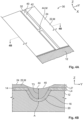
- Figure 1 and Figure 2 illustrate a partial cross-sectional view of a body of an electrically conductive contact element 10 according to a first embodiment of the present invention.
- a contact surface is represented, while in Figure 2 the contact surface is omitted in order to better highlight the structure of the body of the electrically conductive contact element 10.
- Figure 1 and Figure 2 are described together in the following.
- the electrically conductive contact element 10 for an electrical connector comprises a body 12, in particular a metallic body 12.
- the body 12 is delimited by a plurality of faces.
- at least one face 14 of the body 12, said face 14 extending in a plan (XY) in the example of Figures 1 and 2 is provided with a depression 16.
- the depression 16 extends from an opening 18 in the face 14 partially into the body 12 along a direction parallel to the axis Z.
- the depression 16 has a substantially half-spherical shape.
- the diameter L1 of the corresponding circular opening 18 can be greater than 0,05mm, in particular can be comprised between 0,05mm and 0,06mm.
- the maximal depth L2 of the depression 16 is greater than 0,01mm. Namely, the maximal depth L2 of the depression 16 can be greater than 0,03mm, in particular greater than 0,04mm, more in particular greater than 0,05mm.
- the depression 16 can have a groove shape, in particular a rounded groove shape.
- the opening 18 of the depression 16 can have a square shape, a rectangular shape, an oval shape, triangular shape, etc.
- the depression 16 forms a reservoir 20.
- Figure 2 illustrates an empty reservoir 20 in order to better highlight the structure of the depression 16.
- the depression 16 has one open-end 18.
- a layer 22 of an electrically conductive material M of thickness L3 is provided on the face 14 of the body 12.
- the electrically conductive material M is a plating material that can be made of tin, nickel, silver, gold, a tin-nickel alloy, an alloy of tin or nickel-silver alloy.
- the layer 22 of the electrically conductive material M is directly provided on the face 14.
- a surface 24 of the layer 22 facing away from the body 12 of the electrically conductive contact element 10 forms a contact surface 24.
- the contact surface 24 extends substantially in the plane (XY).
- the contact surface 24 is configured to be brought into contact with a surface of a connecting part of a mating electrical connector (not represented).
- the initial stage relates to a stage wherein the electrically conductive contact element 10 has not yet being brought in contact with an electrically conductive contact element of a mating connector.
- the contact surface 24 is substantially flat in the plane (XY).
- Figure 3 illustrates a partial cross-sectional view of a body of an electrically conductive contact element 30 according to a second embodiment of the present invention.
- an adhesion layer 32 is directly provided on the face 14 of the body 12 and sandwiched between the face 14 of the body 12 and the layer 22 of the electrically conductive material M.
- the adhesion layer 32 is provided with a substantially uniform thickness L4 on the face 14, including on the face 14 in the depression 16, as shown in Figure 3 .
- the layer 22 has a thickness L3', wherein L3' ⁇ L3.
- further layers may be sandwiched between the face 14 of the body 12 and the layer 22 of the electrically conductive material M.
- Figure 4A illustrates a top view of the electrically conductive contact element 30 according to the second embodiment of the present invention at a later stage than the initial stage, wherein mechanical and/or chemical wear has occurred.
- Figure 4B illustrates a cross-sectional view of the electrically conductive contact element 30 shown in Figure 4A.
- Figure 4A and Figure 4B are described together in the following.
- the mechanical and/chemical wear has caused a disruption 40 in the contact surface 24 leading to the exposure of the adhesion layer 32.
- the disruption 40 has the shape of a groove 42 extending along the axis X.
- Such linear groove shape may be caused by a back and forth motion of the mating contact surfaces for example.
- Other shapes (not represented) of disruption 40 in the contact surface 24 may occur, depending on the relative motions of the connector and the mating connector for instance.
- the presence of the depression 16 in the body 12 allows providing a reservoir 20 of electrically conductive material M such that at the wear stage of Figures 4A and 4B , a contact area 44 of electrically conductive material M still remains at the contact surface 24 despite the disruption 40.
- Figure 5 illustrates an enlarged view of an electrically conductive contact element 50 according to a third embodiment of the present invention.
- the electrically conductive material M and the optional adhesive layer 52 is not represented in Figure 5 .
- the electrically conductive contact element 50 has a metallic body 52 comprising a frame 54 extending in a plane (XY) and defining an aperture 56.
- a metallic body 52 comprising a frame 54 extending in a plane (XY) and defining an aperture 56.
- Four contact pins 58 extends within the frame 54 across the aperture 56.
- the number of contact pins 58 is not limitative.
- Each contact pins 58 are bent with respect to the plan (XY) such as to be provided with two slightly curved regions R1 and R2. The number of curved regions is not limitative.
- the curved regions R1, R2 consist of the regions of the electrically conductive contact element 50 onto which greater elastic spring forces are exerted in comparison with the rest of the contact pins 58. Elastic spring forces is intended to be exerted on the curved regions R1, R2 by a connecting part of a mating connector applying a pressure on the curved regions R1, R2 in a mating state of the connectors.
- the curved regions R1, R2 are provided with a plurality of depressions 16 formed in the face 14 of the metallic body 52, as previously described in reference to Figures 1 and 2 .
- the location of the plurality of depressions 16 at the curved regions R1, R2 allows improving the wear resistance at the area most subject to mechanical stress, and therefore to wear.
- the plurality of depressions 16 provide a redundancy of improved contact areas, thereby enhancing the reliability and durability of the electrical contact between the electrical connectors.
- Figures 6A , 6B and 6C illustrate successive steps of a method of manufacturing a contact surface of the electrically conductive contact element 50 according to the third embodiment of the present invention.
- the face 14 of the metallic body 12 at the contact pin 58 is substantially uniform.
- each depression 16 has a substantially half-spherical shape.
- the depressions 16 can have a different shape than a substantially half-spherical shape.
- the plurality of depressions 16 can comprise a combination of depressions 16 of different shapes and/or sizes.
- a plating layer 22 of the electrically conductive material M of thickness L5 has been provided on the face 14 of the metallic body 12 thereby coating the face 14 and filling each depression 16 with the electrically conductive material M.
- the surface 24 of the plating layer 22 facing away from the body 52 forms the contact surface 24 of the electrically conductive contact element 50.
Abstract
Description
- The present invention relates to an electrically conductive contact element for a connector which has a contact surface, and an electrical connector comprising such an electrically conductive contact element.
- The present invention further relates to a method of manufacturing the contact surface of an electrically conductive contact element for an electrical connector.
- Electrical connectors are generally used for signal or power transmission and to link electrical and electronic systems. Electrical connectors are provided with electrically conductive contact elements, which come into contact with a contact element of a mating electrical connector when the electrical connector is plugged to the mating electrical connector. The contact elements of the connector element are commonly formed as contact pins and those of the mating connector are commonly formed as contact springs. When the connector and mating connector are coupled, the contact springs exert elastic spring forces on the contact pins and thereby provide an electrical connection between the contact elements.
- The quality of the electrical connection may be affected by mechanical and/or chemical degradations occurring at the contact surfaces of the contact elements. The respective contact surface of the electrically conductive contact elements may be coated with a layer of tin, nickel or alloys thereof.
- As in motor vehicles, electrical connectors may be exposed to broad temperature variations, vibrations and corrosive environment, it can cause damages to the layer coating the contact surface. Fretting corrosion is known as a degradation resulting from the combination of a mechanical motion and a chemical reaction. The combination of the relative motion of mated contact surfaces, causing fretting wear, with corrosion (like oxidation) may lead to fretting corrosion. Fretting corrosion leads to the formation of insulating oxide layers in contact areas and can cause an increase of the electrical contact resistance. Moreover, wear damages, like abrasion, at the contact surfaces of the contact elements may also lead to an increase of the electrical constriction resistance. As the performance of the electrical connector is related to the reliability of the electrical contacts, there is a need for preventing wear damage at the contact surfaces so as to avoid malfunction due to the increase in electrical resistance.
- Along with improving wear and corrosion resistance, low plugging and pulling forces are required in order to facilitate the mounting and maintenance of electrical connectors. In order to reduce the plugging force, the surface wear or fretting corrosion, the contact surfaces of the connectors from the prior art are oiled or greased. However, greased or oiled contact surfaces lose the applied grease or oil when in operation. For addressing this drawback related to the use of grease or oil in the contact surfaces, it is known from
US 2019/0173214 A1 to provide an electrically conductive contact element for an electrical connector comprising a contact surface having a plurality of caverns arranged under the contact surface in a microstructure and having a lubricant filled and enclosed in the plurality of caverns. The spatial dimensions in the caverns according toUS 2019/0173214 A1 is in the range of 0,1-50 micrometers. The arrangement of the caverns according toUS 2019/0173214 A1 under the contact surface is such that an outlet of the cavern is tight enough so that the lubricant filled into the caverns cannot be accessed without establishing an opening from the contact surfaces into the cavern. Manufacturing the microstructureUS 2019/0173214 A1 requires the use of a laser, an electron beam or surface treatment like masking and etching. - The object of the present invention is to provide an improved and cost effective contact element for a connector which can better withstand wear so as to reduce the contact resistance while reducing the mating force to ease the assembly and the maintenance of the connector, in particular without the need of using lubricant.
- The object of the present invention is achieved by means of an electrically conductive contact element for an electrical connector according to claim 1. The electrically conductive contact element has a contact surface configured to be brought into contact with a surface of a connecting part of a mating electrical connector adapted to be mated with the electrical connector. The electrically conductive contact element comprises: a body and a layer of an electrically conductive material provided on a first face of said body, wherein the contact surface is formed by a surface of said layer facing away from the body. The first face of the body comprises at least one depression forming a reservoir filled with the electrically conductive material.
- At the at least one depression, the electrically conductive contact element is provided with the electrically conductive material contained in the layer as well as with the electrically conductive material filled in the reservoir. Hence, at the at least one depression, under the contact surface, there is more electrically conductive material than in the rest of the electrically conductive contact element, wherein the first face of the body is covered by the layer of the electrically conductive material. As a result, an uneven wear of the contact surface is caused, such that presence of the electrically conductive material can last longer at the at least one depression. Consequently, the at least one depression provides a contact area that is preserved longer from mechanical wear and corrosion during the lifetime of the electrically conductive contact element. Accordingly, the resistance to the outdoor environment, like corrosive media and the electrical constriction resistance at the at least one depression is improved over the lifetime of the electrically conductive contact element with respect to the known contact element. It allows increasing the durability of an electrical connector comprising such electrically conductive contact element by preventing, or at least delaying, a malfunction of the connector related to the quality of the electrical contact. Moreover, as the presence of electrically conductive material allows reducing the required mating force thank to the mechanical properties of the electrically conductive material, the ease of assembly, plugging and handling of a related electrical connector can be enhanced.
- The electrically conductive contact element can be further improved according to various advantageous embodiments. The embodiments are disclosed in the dependent claims.
- According to one embodiment, the electrically conductive material filled in the reservoir can be configured to come in contact with a surface of a connecting part of the mating electrical connector.
- Hence, the reservoir has a direct output at the contact surface. It allows directly exposing the electrically conductive material to a mating contact surface.
- According to one embodiment, the body can be made of metal and the electrically conductive material can be a plating material made of tin, nickel, silver, gold, a tin-nickel alloy, an alloy of tin or a nickel-silver alloy.
- Electrically conductive materials are selected so as to enable an electrical connection between electrical connectors.
- The plating material can be selected based on its resistance to mechanical wear and/or corrosion, as well as its cost and availability.
- According to one embodiment, a minimum dimension of the at least one depression in a plan of the contact surface can be greater than 0,05mm, in particular can be comprised between 0,05mm and 0,06mm.
- Hence, given the dimension of the at least one depression, the at least one depression does not form a microstructure in the first face of the body. Hence, it is possible to use simpler and more cost-effective processes, like metal punching, for forming the macroscopic scale depression than manufacturing means require for forming a microstructure, like laser, electron beam or masking and etching.
- It is noted that wording "greater" is to be read as "equal or greater", and not "strictly greater".
- According to one embodiment, a maximal depth of the at least one depression can be greater than 0,03mm, in particular greater than 0,04mm, more in particular more than 0,05mm.
- As mentioned above, given the dimension of the at least one depression, the at least one depression does not form a microstructure in the first face of the body. Hence, it is possible to use simpler and more cost-effective processes, like metal punching, for forming the macroscopic scale depression than manufacturing means require for forming a microstructure, like laser, electron beam or masking and etching.
- Moreover, the maximal depth can be adapted so as to improve further and longer the resistance to wear, by increasing the size of the reservoir of electrically conductive material.
- It is noted that wording "greater" is to be read as "equal or greater", and not "strictly greater".
- According to one embodiment, the at least one depression can have a half-spherical shape or a groove shape, in particular a rounded groove shape.
- Half-spherical and round shapes allow avoiding the presence of sharp edges and optimizing the amount of electrically conductive material filled in the reservoir.
- A groove shape allows providing reservoir that may advantageously extend along a direction of a back and forth motion of the mating contact surfaces, for example a motion caused by vibrations.
- According to one embodiment, the electrically conductive contact element can further comprise an adhesion layer provided on the first face of the body and sandwiched between the first face and the layer of the electrically conductive material.
- The quality of the electrical contact over time can be further improved by the use of an adhesion layer.
- According to one embodiment, in the at least one depression, a thickness of the electrically conductive material can be greater than a thickness of the adhesion layer.
- Hence, in spite of the presence of the adhesion layer, the reservoir is filled with a sufficient amount of electrically conductive material to provide the technical effects of improving the resistance to wear and corrosion and reducing the electrical constriction resistance and the required mating force.
- According to one embodiment, the adhesion layer can be made of nickel, copper or tin.
- According to one embodiment, the electrically conductive contact element can comprise a plurality of depressions and a minimum spacing distance between the depressions can be comprised between 0,10mm and 0,15mm.
- The plurality of depressions provide a redundancy of improved contact areas, thereby enhancing the reliability and durability of the electrical contact between electrical connectors.
- According to one embodiment, the first face of the body can comprise at least one curved region curved in at least one direction and the at least one depression can be arranged at the at least one curved region.
- Curved region can provide a region that is more subjected to deformation than the other regions under elastic spring forces. By increasing the mechanical contact performance at the curved region, the electrical contact performance can be improved as well. Hence, it is particularly advantageous to arrange the at least one depression at the curved region.
- According to one embodiment, the first face of the body can comprise a plurality of depressions of different shapes and/or sizes.
- Hence, the design of the depressions can be advantageously adapted to the contact zone with a mating connector based on the force applied, the size of the contact zone etc.
- According to one embodiment, the electrically conductive contact element can be comprised in an electrical connector configured to be coupled with a mating electrical connector.
- The object of the invention is further achieved by means of an electrical connector configured to be coupled with a mating electrical connector, comprising an electrically conductive contact element. Said electrically conductive contact element comprising: a body having at least a first face, and a layer of an electrically conductive material provided on said first face of the body, the first face of the body comprising at least one depression forming a reservoir filled with the electrically conductive material, and a contact surface configured to be brought into contact with a surface of a connecting part of a mating electrical connector and formed by a surface of said layer of the electrically conductive material facing away from the body.
- In the electrical connector according to the present invention, at the at least one depression, the electrically conductive contact element is provided under the contact surface with the electrically conductive material contained in the layer as well as with the electrically conductive material filled in the reservoir. Hence, at the at least one depression, the contact surface made of the electrically conductive material is thicker than in the rest of the electrically conductive contact element. As a result, an uneven wear of the contact surface is caused, such that presence of the electrically conductive material can be maintained longer at the at least one depression. Consequently, the at least one depression provides a contact area that is preserved longer from mechanical wear and corrosion during the lifetime of the electrically conductive contact element of the electrical connector. Accordingly, the resistance to the outdoor environment, like corrosive media and the electrical constriction resistance at the at least one depression is improved over the lifetime of the electrically conductive contact element of the electrical connector with respect to the known electrical connectors. It allows increasing the durability of the electrical connector by preventing, or at least delaying, a malfunction of the connector related to the quality of the electrical contact. Moreover, as the presence of electrically conductive material allows reducing the required mating force thank to the mechanical properties of the electrically conductive material, the ease of assembly, plugging and handling of the electrical connector can be enhanced.
- The object of the invention is also achieved by a method of manufacturing a contact surface of an electrically conductive contact element, comprising the steps of: a) forming at least one depression in a first face of a body of the electrically conductive contact element, in particular by metal punching, and then b) applying a layer of an electrically conductive material on the first face including filling the at least one depression with the electrically conductive material.
- Hence, an easy and cost-effective manufacturing process can be used to form the contact surface.
- The method of manufacturing allows providing a contact surface wherein at the at least one depression, under the contact surface, there is more electrically conductive material than in the rest of the electrically conductive contact element, wherein the first face of the body is covered by the layer of the electrically conductive material. As a result, an uneven wear of the contact surface is caused, such that presence of the electrically conductive material can last longer at the at least one depression. Consequently, the at least one depression provides a contact area that is preserved longer from mechanical wear and corrosion during the lifetime of the electrically conductive contact element. Accordingly, the resistance to the outdoor environment, like corrosive media and the electrical constriction resistance at the at least one depression is improved over the lifetime of the electrically conductive contact element with respect to the known contact element. It allows increasing the durability of an electrical connector comprising such electrically conductive contact element by preventing, or at least delaying, a malfunction of the connector related to the quality of the electrical contact. Moreover, as the presence of electrically conductive material allows reducing the required mating force thank to the mechanical properties of the electrically conductive material, the ease of assembly, plugging and handling of a related electrical connector can be enhanced.
- According to one embodiment, the method of manufacturing can further comprise, before the step b), a step of applying an adhesion layer on the contact surface.
- The step of adding an adhesion layer allows further improving the quality of the electrical contact throughout the lifetime of the electrical connector.
- The accompanying drawings are incorporated into the specification and form a part of the specification to illustrate several embodiments of the present invention. These drawings, together with the description serve to explain the principles of the invention. The drawings are merely for the purpose of illustrating the preferred and alternative examples of how the invention can be made and used, and are not to be construed as limiting the invention to only the illustrated and described embodiments. Furthermore, several aspects of the embodiments may form - individually or in different combinations - solutions according to the present invention. The following described embodiments thus can be considered either alone or in an arbitrary combination thereof. Further features and advantages will become apparent from the following more particular description of the various embodiments of the invention, as illustrated in the accompanying drawings, in which like references refer to like elements, and wherein:
-
Figure 1 illustrates a partial cross-sectional view of an electrically conductive contact element according to a first embodiment of the present invention at an initial stage. -
Figure 2 illustrates a body of the electrically conductive contact element shown inFigure 1 . -
Figure 3 illustrates a partial cross-sectional view of an electrically conductive contact element according to a second embodiment of the present invention at an initial stage. -
Figure 4A illustrates a top view of the electrically conductive contact element according to the second embodiment of the present invention at a later stage than the initial stage. -
Figure 4B illustrates a cross-sectional view of the electrically conductive contact element shown inFigure 4A . -
Figure 5 illustrates an enlarged view of a body of an electrically conductive contact element according to a third embodiment of the present invention. -
Figures 6A, 6B and 6C illustrate successive steps of a method of manufacturing a contact surface of the electrically conductive contact element according to the third embodiment of the present invention. - All previously discussed embodiments are not intended as limitations but serve as examples illustrating features and advantages of the invention. It is to be understood that some or all of the above described features can also be combined in different ways.
-
Figure 1 and Figure 2 illustrate a partial cross-sectional view of a body of an electricallyconductive contact element 10 according to a first embodiment of the present invention. InFigure 1 , a contact surface is represented, while inFigure 2 the contact surface is omitted in order to better highlight the structure of the body of the electricallyconductive contact element 10.Figure 1 and Figure 2 are described together in the following. - The electrically
conductive contact element 10 for an electrical connector (not represented) comprises abody 12, in particular ametallic body 12. Thebody 12 is delimited by a plurality of faces. According to the present invention, at least oneface 14 of thebody 12, saidface 14 extending in a plan (XY) in the example ofFigures 1 and 2 , is provided with adepression 16. Thedepression 16 extends from anopening 18 in theface 14 partially into thebody 12 along a direction parallel to the axis Z. - In the first embodiment, the
depression 16 has a substantially half-spherical shape. The diameter L1 of the correspondingcircular opening 18 can be greater than 0,05mm, in particular can be comprised between 0,05mm and 0,06mm. - The maximal depth L2 of the
depression 16 is greater than 0,01mm. Namely, the maximal depth L2 of thedepression 16 can be greater than 0,03mm, in particular greater than 0,04mm, more in particular greater than 0,05mm. - It is noted that wording "greater" is to be read as "equal or greater", and not "strictly greater".
- In a variant, the
depression 16 can have a groove shape, in particular a rounded groove shape. In another variant, theopening 18 of thedepression 16 can have a square shape, a rectangular shape, an oval shape, triangular shape, etc. - The
depression 16 forms areservoir 20.Figure 2 illustrates anempty reservoir 20 in order to better highlight the structure of thedepression 16. As mentioned above and emphasized inFigure 2 , thedepression 16 has one open-end 18. - As shown in
Figure 1 , alayer 22 of an electrically conductive material M of thickness L3 is provided on theface 14 of thebody 12. The electrically conductive material M is a plating material that can be made of tin, nickel, silver, gold, a tin-nickel alloy, an alloy of tin or nickel-silver alloy. - In the first embodiment, the
layer 22 of the electrically conductive material M is directly provided on theface 14. - A
surface 24 of thelayer 22 facing away from thebody 12 of the electricallyconductive contact element 10 forms acontact surface 24. Thecontact surface 24 extends substantially in the plane (XY). Thecontact surface 24 is configured to be brought into contact with a surface of a connecting part of a mating electrical connector (not represented). - As shown at the initial stage represented in
Figure 1 , in the first embodiment, a thickness T1 of electrically conductive material M is provided above a deepest point A of thereservoir 20, wherein T1= L2+L3. - The initial stage relates to a stage wherein the electrically
conductive contact element 10 has not yet being brought in contact with an electrically conductive contact element of a mating connector. Hence, at the initial stage mechanical wear, corrosion, abrasion or any damages that may result from the mating surfaces have not yet occurred. That is why in the initial stage, as shown inFigure 1 , thecontact surface 24 is substantially flat in the plane (XY). - In the following, elements with the same reference numeral already described and illustrated with respect to
Figures 1 and 2 will not necessarily be described in detail again, but reference is made to the previous description of the same reference numeral. -
Figure 3 illustrates a partial cross-sectional view of a body of an electricallyconductive contact element 30 according to a second embodiment of the present invention. - In comparison to the first embodiment, in the second embodiment an
adhesion layer 32 is directly provided on theface 14 of thebody 12 and sandwiched between theface 14 of thebody 12 and thelayer 22 of the electrically conductive material M. - The
adhesion layer 32 is provided with a substantially uniform thickness L4 on theface 14, including on theface 14 in thedepression 16, as shown inFigure 3 . - In the second embodiment, the
layer 22 has a thickness L3', wherein L3' ≤ L3. - As shown in the initial stage represented in
Figure 3 , in the second embodiment, a thickness T2 of electrically conductive material M is provided above the deepest point A of thereservoir 20, wherein T2=L3'+(L2-L4). - In a variant (not represented), further layers may be sandwiched between the
face 14 of thebody 12 and thelayer 22 of the electrically conductive material M. -
Figure 4A illustrates a top view of the electricallyconductive contact element 30 according to the second embodiment of the present invention at a later stage than the initial stage, wherein mechanical and/or chemical wear has occurred.Figure 4B illustrates a cross-sectional view of the electricallyconductive contact element 30 shown inFigure 4A. Figure 4A and Figure 4B are described together in the following. - In the following, elements with the same reference numeral already described and illustrated with respect to
Figures 1 to 3 will not necessarily be described in detail again, but reference is made to the previous description of the same reference numeral. - In the stage of wear shown in
Figures 4A, 4B , the mechanical and/chemical wear has caused adisruption 40 in thecontact surface 24 leading to the exposure of theadhesion layer 32. At a later stage (not represented), the further removal of theadhesion layer 32 could lead to the exposure of theface 14 of thebody 12. In the example ofFigure 4A , thedisruption 40 has the shape of agroove 42 extending along the axis X. Such linear groove shape may be caused by a back and forth motion of the mating contact surfaces for example. Other shapes (not represented) ofdisruption 40 in thecontact surface 24 may occur, depending on the relative motions of the connector and the mating connector for instance. - According to the present invention, the presence of the
depression 16 in thebody 12 allows providing areservoir 20 of electrically conductive material M such that at the wear stage ofFigures 4A and 4B , acontact area 44 of electrically conductive material M still remains at thecontact surface 24 despite thedisruption 40. - As shown in
Figure 4B , in the wear stage represented inFigures 4A and 4B , a thickness T3, wherein T3<T2, of electrically conductive material M above the deepest point A of thedepression 16 still remains in thereservoir 20. Hence, an uneven wear at thecontact surface 24 is achieved allowing providing at least onecontact area 44 of low electrical contact resistance. - It is noted that the same effect of providing a
contact area 44 of electrically conductive material M would occur in the electricallyconductive contact element 10 according to the first embodiment. In contrast with the second embodiment, adisruption 40 in thecontact surface 24 in thecontact element 10 according to the first embodiment would lead to expose directly theface 14 of thebody 12, due to the absence of an adhesion layer. -
Figure 5 illustrates an enlarged view of an electricallyconductive contact element 50 according to a third embodiment of the present invention. In order to show thedepressions 16 formed in the electricallyconductive contact element 50, the electrically conductive material M and theoptional adhesive layer 52 is not represented inFigure 5 . - The electrically
conductive contact element 50 according to a third embodiment has ametallic body 52 comprising aframe 54 extending in a plane (XY) and defining anaperture 56. Four contact pins 58 extends within theframe 54 across theaperture 56. The number of contact pins 58 is not limitative. Each contact pins 58 are bent with respect to the plan (XY) such as to be provided with two slightly curved regions R1 and R2. The number of curved regions is not limitative. - The curved regions R1, R2 consist of the regions of the electrically
conductive contact element 50 onto which greater elastic spring forces are exerted in comparison with the rest of the contact pins 58. Elastic spring forces is intended to be exerted on the curved regions R1, R2 by a connecting part of a mating connector applying a pressure on the curved regions R1, R2 in a mating state of the connectors. - The curved regions R1, R2 are provided with a plurality of
depressions 16 formed in theface 14 of themetallic body 52, as previously described in reference toFigures 1 and 2 . - The
depressions 16 of the plurality ofdepressions 16 are spaced away from each other by a minimal distance d1, wherein d1 is comprised between 0,10mm and 0,15mm. In particular, d1=0,125mm. - The location of the plurality of
depressions 16 at the curved regions R1, R2 allows improving the wear resistance at the area most subject to mechanical stress, and therefore to wear. - The plurality of
depressions 16 provide a redundancy of improved contact areas, thereby enhancing the reliability and durability of the electrical contact between the electrical connectors. -
Figures 6A, 6B and 6C illustrate successive steps of a method of manufacturing a contact surface of the electricallyconductive contact element 50 according to the third embodiment of the present invention. - At the step represented by
Figure 6A , theface 14 of themetallic body 12 at thecontact pin 58 is substantially uniform. - At the step represented by
Figure 6B , a plurality ofdepressions 16 has been formed by metal punching in theface 14 of themetallic body 12 at thecontact pin 58. In the example ofFigure 6A , eachdepression 16 has a substantially half-spherical shape. In a variant (not represented), thedepressions 16 can have a different shape than a substantially half-spherical shape. In another variant (not represented), the plurality ofdepressions 16 can comprise a combination ofdepressions 16 of different shapes and/or sizes. - At the last step of the manufacturing method represented by
Figure 6C , aplating layer 22 of the electrically conductive material M of thickness L5 has been provided on theface 14 of themetallic body 12 thereby coating theface 14 and filling eachdepression 16 with the electrically conductive material M. - The
surface 24 of theplating layer 22 facing away from thebody 52 forms thecontact surface 24 of the electricallyconductive contact element 50. - All previously discussed embodiments are not intended as limitations but serve as examples illustrating features and advantages of the invention. It is to be understood that some or all of the above described features can also be combined in different ways. It is noted that an individual feature described in relation with one embodiment can be combined with another embodiment.
-
- 10:
- electrically conductive contact element according to the first embodiment
- 12:
- body
- 14:
- (first) face of the body
- 16:
- depression
- 18:
- opening of the depression
- 20:
- reservoir
- 22:
- layer
- 24:
- contact surface
- 30:
- electrically conductive contact element according to the second embodiment
- 32:
- adhesion layer
- 40:
- disruption in a wear stage
- 42:
- groove in a wear stage
- 44:
- contact area in a wear stage
- 50:
- electrically conductive contact element according to the third embodiment
- 52:
- metallic body
- 54:
- frame
- 56:
- aperture
- 58:
- contact pins
- A:
- deepest zone of the
depression 16 - d1:
- spacing distances between
depressions 16 - L1:
- diameter of the
depression 16 - L2:
- maximal depth of the
depression 16 - L3, L3':
- thickness of the
layer 22 of the electrically conductive material M - L4:
- thickness of the
adhesion layer 32 - L5:
- thickness of the
layer 22 of the electrically conductive material M - M:
- electrically conductive material
- T1, T2, T3:
- maximum thickness of the electrically conductive material M
- R1. R2:
- curved regions of the
contact pin 58
Claims (15)
- An electrically conductive contact element (10, 30, 50) for an electrical connector, having a contact surface (24) configured to be brought into contact with a surface of a connecting part of a mating electrical connector adapted to be mated with the electrical connector, the electrically conductive contact element (10, 30, 50) comprising:a body (12, 52) and a layer (22) of an electrically conductive material (M) provided on a first face (14) of said body (12, 52),wherein the contact surface (24) is formed by a surface (24) of said layer (22) facing away from the body (12, 52),the electrically conductive contact element (10, 30, 50) being characterized in that
the first face (14) of the body (12, 52) comprises at least one depression (16) forming a reservoir (20) filled with the electrically conductive material (M). - The electrically conductive contact element according to claim 1, wherein the electrically conductive material (M) filled in the reservoir (16) is configured to come in contact with a surface of the connecting part of the mating electrical connector.
- The electrically conductive contact element according to claim 1 or 2, wherein the body (12, 52) is made of metal and the electrically conductive material (M) is a plating material made of tin, nickel, silver, gold, a tin-nickel alloy, an alloy of tin or a nickel-silver alloy.
- The electrically conductive contact element according to one of the preceding claims, wherein a minimum dimension (L1) of the at least one depression (16, 18) in a plan of the first face (14) of the body (12, 52) is greater than 0,05mm, in particular is comprised between 0,05mm and 0,06mm.
- The electrically conductive contact element according to one of the preceding claims, wherein a maximal depth (L2) of the at least one depression (16) is greater than 0,03mm, in particular greater than 0,04mm, more in particular greater than 0,05mm.
- The electrically conductive contact element according to one of the preceding claims, wherein the at least one depression (16) has a half-spherical shape or a groove shape, in particular a rounded groove shape.
- The electrically conductive contact element according to one of the preceding claims, further comprising an adhesion layer (32) provided on the first face (14) of the body (12, 52) and sandwiched between the first face (14) of the body (12, 52) and the layer (22) of the electrically conductive material (M).
- The electrically conductive contact element according to claim 7, wherein in the at least one depression (16), a thickness (L3') of the electrically conductive material (M) is greater than a thickness (L4) of the adhesion layer (32).
- The electrically conductive contact element according to claim 7 or 8, wherein the adhesion layer (32) is made of nickel, copper or tin.
- The electrically conductive contact element according to one of the preceding claims, comprising a plurality of depressions (16) and a minimum spacing distance (d1) between the depressions (16) is comprised between 0,10mm and 0,15mm.
- The electrically conductive contact element according to one of the preceding claims, wherein the first face (14) of the body (12) comprises at least one curved region (R1, R2) curved in at least one direction and the at least one depression (16) is arranged at the at least one curved region (R1, R2).
- The electrically conductive contact element according to one of the preceding claims, wherein the first face (14) of the body (12) comprises a plurality of depressions (16) of different shapes and/or sizes.
- An electrical connector configured to be coupled with a mating electrical connector, comprising:
an electrically conductive contact element (10, 30, 50) comprising:a body (12, 52) having at least a first face (14), anda layer (22) of an electrically conductive material (M) provided on said first face (14) of the body (12, 52), andthe first face (14) of the body (12, 52) comprising at least one depression (16) forming a reservoir (20) filled with the electrically conductive material, anda contact surface (24) configured to be brought into contact with a surface of a connecting part of a mating electrical connector and formed by a surface (24) of the layer (22) of the electrically conductive material (M) facing away from the body (12, 52). - Method of manufacturing a contact surface of an electrically conductive contact element, comprising the steps of:a) forming at least one depression (16) in a first face (14) of a body (12, 52) of the electrically conductive contact element, in particular by metal punching, and thenb) applying a layer (22) of an electrically conductive material (M) on the first face (14) including filling the at least one depression (16) with the electrically conductive material (M).
- Method according to claim 14, further comprising, before the step b), a step of applying an adhesion layer (32) on the first face (14) of the body (52) of the electrically conductive contact element (30).
Priority Applications (5)
| Application Number | Priority Date | Filing Date | Title |
|---|---|---|---|
| EP21306644.2A EP4187723A1 (en) | 2021-11-25 | 2021-11-25 | Electrically conductive contact element for a connector |
| JP2022185380A JP2023078092A (en) | 2021-11-25 | 2022-11-21 | Electrically conductive contact element for connector |
| CN202211466205.XA CN116169500A (en) | 2021-11-25 | 2022-11-22 | Conductive contact element for connector |
| KR1020220158285A KR20230077681A (en) | 2021-11-25 | 2022-11-23 | Electrically conductive contact element for a connector |
| US17/993,151 US20230163504A1 (en) | 2021-11-25 | 2022-11-23 | Electrically Conductive Contact Element for a Connector |
Applications Claiming Priority (1)
| Application Number | Priority Date | Filing Date | Title |
|---|---|---|---|
| EP21306644.2A EP4187723A1 (en) | 2021-11-25 | 2021-11-25 | Electrically conductive contact element for a connector |
Publications (1)
| Publication Number | Publication Date |
|---|---|
| EP4187723A1 true EP4187723A1 (en) | 2023-05-31 |
Family
ID=78851028
Family Applications (1)
| Application Number | Title | Priority Date | Filing Date |
|---|---|---|---|
| EP21306644.2A Pending EP4187723A1 (en) | 2021-11-25 | 2021-11-25 | Electrically conductive contact element for a connector |
Country Status (5)
| Country | Link |
|---|---|
| US (1) | US20230163504A1 (en) |
| EP (1) | EP4187723A1 (en) |
| JP (1) | JP2023078092A (en) |
| KR (1) | KR20230077681A (en) |
| CN (1) | CN116169500A (en) |
Citations (4)
| Publication number | Priority date | Publication date | Assignee | Title |
|---|---|---|---|---|
| US20080257581A1 (en) * | 2007-04-20 | 2008-10-23 | Kabushiki Kaisha Kobe Seiko Sho (Kobe Steel, Ltd) | Terminal for engaging type connector |
| US20130014979A1 (en) * | 2011-07-15 | 2013-01-17 | Tessera, Inc. | Connector Structures and Methods |
| US20190173214A1 (en) | 2016-08-08 | 2019-06-06 | Te Connectivity Germany Gmbh | Electrical Contact Element For An Electrical Connector Having Microstructured Caverns Under The Contact Surface |
| WO2020049988A1 (en) * | 2018-09-06 | 2020-03-12 | 株式会社デンソー | Plated product production method |
-
2021
- 2021-11-25 EP EP21306644.2A patent/EP4187723A1/en active Pending
-
2022
- 2022-11-21 JP JP2022185380A patent/JP2023078092A/en active Pending
- 2022-11-22 CN CN202211466205.XA patent/CN116169500A/en active Pending
- 2022-11-23 US US17/993,151 patent/US20230163504A1/en active Pending
- 2022-11-23 KR KR1020220158285A patent/KR20230077681A/en unknown
Patent Citations (4)
| Publication number | Priority date | Publication date | Assignee | Title |
|---|---|---|---|---|
| US20080257581A1 (en) * | 2007-04-20 | 2008-10-23 | Kabushiki Kaisha Kobe Seiko Sho (Kobe Steel, Ltd) | Terminal for engaging type connector |
| US20130014979A1 (en) * | 2011-07-15 | 2013-01-17 | Tessera, Inc. | Connector Structures and Methods |
| US20190173214A1 (en) | 2016-08-08 | 2019-06-06 | Te Connectivity Germany Gmbh | Electrical Contact Element For An Electrical Connector Having Microstructured Caverns Under The Contact Surface |
| WO2020049988A1 (en) * | 2018-09-06 | 2020-03-12 | 株式会社デンソー | Plated product production method |
Also Published As
| Publication number | Publication date |
|---|---|
| JP2023078092A (en) | 2023-06-06 |
| KR20230077681A (en) | 2023-06-01 |
| US20230163504A1 (en) | 2023-05-25 |
| CN116169500A (en) | 2023-05-26 |
Similar Documents
| Publication | Publication Date | Title |
|---|---|---|
| CN105706308B (en) | Electrical connection device | |
| KR101389172B1 (en) | Female terminal fitting and production method therefor | |
| JP7453280B2 (en) | connector system | |
| EP2752945B1 (en) | Mating-type connection terminal, and manufacturing method therefor | |
| CN111149003B (en) | Conductive contact and anisotropic conductive sheet having the same | |
| KR20010015447A (en) | Test socket, method of manufacturing the test socket, test method using the test socket, and member to be tested | |
| EP3089277B1 (en) | In-vehicle electronic module | |
| US20160344127A1 (en) | Electroconductive material with an undulating surface, an electrical terminal formed of said material, and a method of producing said material | |
| EP2904666B1 (en) | Electrical contact assembly | |
| EP2978076B1 (en) | Electrical connector, and socket for electric component | |
| KR20080027182A (en) | Connecting device | |
| EP4187723A1 (en) | Electrically conductive contact element for a connector | |
| WO2017126283A1 (en) | Vehicle-mounted electronic module, card edge connector, and connector | |
| JP2016225173A (en) | Press-fit terminal, electronic device, and press-fitting method of press-fit terminal | |
| US11664617B2 (en) | Electrical terminal, method for manufacturing elastic terminal, electrical connector and electronic device | |
| US20170162969A1 (en) | Terminal pair and connector | |
| KR20150123182A (en) | Method for producing an electrical contact element for preventing tin whisker formation, and contact element | |
| US10424889B2 (en) | Stabilized gold wire brush for sliprings | |
| JP6244170B2 (en) | Conductive member for connector | |
| CN108140970B (en) | Electrical contact and socket for electrical component | |
| JP6930509B2 (en) | Manufacturing method of plated products | |
| CN104901041A (en) | Connecting pin for electronic circuit boards | |
| JP2015210863A (en) | Contact connection structure | |
| EP0748000A2 (en) | Electrical connector | |
| JP2020145142A (en) | Electronic device and press-fit terminal |
Legal Events
| Date | Code | Title | Description |
|---|---|---|---|
| PUAI | Public reference made under article 153(3) epc to a published international application that has entered the european phase |
Free format text: ORIGINAL CODE: 0009012 |
|
| STAA | Information on the status of an ep patent application or granted ep patent |
Free format text: STATUS: THE APPLICATION HAS BEEN PUBLISHED |
|
| AK | Designated contracting states |
Kind code of ref document: A1 Designated state(s): AL AT BE BG CH CY CZ DE DK EE ES FI FR GB GR HR HU IE IS IT LI LT LU LV MC MK MT NL NO PL PT RO RS SE SI SK SM TR |
|
| STAA | Information on the status of an ep patent application or granted ep patent |
Free format text: STATUS: REQUEST FOR EXAMINATION WAS MADE |
|
| 17P | Request for examination filed |
Effective date: 20231123 |
|
| RBV | Designated contracting states (corrected) |
Designated state(s): AL AT BE BG CH CY CZ DE DK EE ES FI FR GB GR HR HU IE IS IT LI LT LU LV MC MK MT NL NO PL PT RO RS SE SI SK SM TR |