EP4187451B1 - Supraleitendes chip-gehäuse mit verbesserter magnetischer abschirmung - Google Patents
Supraleitendes chip-gehäuse mit verbesserter magnetischer abschirmung Download PDFInfo
- Publication number
- EP4187451B1 EP4187451B1 EP21210843.5A EP21210843A EP4187451B1 EP 4187451 B1 EP4187451 B1 EP 4187451B1 EP 21210843 A EP21210843 A EP 21210843A EP 4187451 B1 EP4187451 B1 EP 4187451B1
- Authority
- EP
- European Patent Office
- Prior art keywords
- shield
- package
- shell portion
- pillars
- superconducting
- Prior art date
- Legal status (The legal status is an assumption and is not a legal conclusion. Google has not performed a legal analysis and makes no representation as to the accuracy of the status listed.)
- Active
Links
Images
Classifications
-
- H—ELECTRICITY
- H10—SEMICONDUCTOR DEVICES; ELECTRIC SOLID-STATE DEVICES NOT OTHERWISE PROVIDED FOR
- H10N—ELECTRIC SOLID-STATE DEVICES NOT OTHERWISE PROVIDED FOR
- H10N60/00—Superconducting devices
- H10N60/80—Constructional details
- H10N60/81—Containers; Mountings
-
- H—ELECTRICITY
- H10—SEMICONDUCTOR DEVICES; ELECTRIC SOLID-STATE DEVICES NOT OTHERWISE PROVIDED FOR
- H10W—GENERIC PACKAGES, INTERCONNECTIONS, CONNECTORS OR OTHER CONSTRUCTIONAL DETAILS OF DEVICES COVERED BY CLASS H10
- H10W42/00—Arrangements for protection of devices
- H10W42/20—Arrangements for protection of devices protecting against electromagnetic or particle radiation, e.g. light, X-rays, gamma-rays or electrons
- H10W42/281—Arrangements for protection of devices protecting against electromagnetic or particle radiation, e.g. light, X-rays, gamma-rays or electrons characterised by their materials
- H10W42/287—Arrangements for protection of devices protecting against electromagnetic or particle radiation, e.g. light, X-rays, gamma-rays or electrons characterised by their materials materials for magnetic shielding, e.g. ferromagnetic materials
-
- H—ELECTRICITY
- H10—SEMICONDUCTOR DEVICES; ELECTRIC SOLID-STATE DEVICES NOT OTHERWISE PROVIDED FOR
- H10W—GENERIC PACKAGES, INTERCONNECTIONS, CONNECTORS OR OTHER CONSTRUCTIONAL DETAILS OF DEVICES COVERED BY CLASS H10
- H10W76/00—Containers; Fillings or auxiliary members therefor; Seals
- H10W76/10—Containers or parts thereof
- H10W76/12—Containers or parts thereof characterised by their shape
- H10W76/15—Containers comprising an insulating or insulated base
-
- G—PHYSICS
- G06—COMPUTING OR CALCULATING; COUNTING
- G06N—COMPUTING ARRANGEMENTS BASED ON SPECIFIC COMPUTATIONAL MODELS
- G06N10/00—Quantum computing, i.e. information processing based on quantum-mechanical phenomena
- G06N10/40—Physical realisations or architectures of quantum processors or components for manipulating qubits, e.g. qubit coupling or qubit control
-
- H—ELECTRICITY
- H10—SEMICONDUCTOR DEVICES; ELECTRIC SOLID-STATE DEVICES NOT OTHERWISE PROVIDED FOR
- H10W—GENERIC PACKAGES, INTERCONNECTIONS, CONNECTORS OR OTHER CONSTRUCTIONAL DETAILS OF DEVICES COVERED BY CLASS H10
- H10W44/00—Electrical arrangements for controlling or matching impedance
- H10W44/20—Electrical arrangements for controlling or matching impedance at high-frequency [HF] or radio frequency [RF]
Definitions
- the present invention is related to a package for housing one or more superconducting chips, for example qubit chips which are applicable in quantum computing, quantum metrology and quantum sensing.
- the qubit chip is cooled to a temperature ⁇ 10 mK in a dilution refrigerator.
- the chip is enclosed in a metallic sample box which is then attached to the lowest temperature stage of the dilution refrigerator.
- This is followed by several layers of electrical and magnetic shields on different thermal stages to further attenuate the impact of external EM and thermal noise.
- the sample box and the electrical shields are typically made from oxygen-free-high-conductivity (OFHC) copper whereas the magnetic shields are built from superconducting materials and/or high magnetic permeability nickel alloy materials.
- the sample box which houses the chip and the coplanar-waveguide (CPW) based printed-circuit board (PCB) with connectors (for signal routing), is placed inside a cylindrical-shaped magnetic shield.
- CPW coplanar-waveguide
- PCB printed-circuit board
- the sample box also serves to shield the PCB from EM noise.
- This setup is ideal for a sample box with a compact-connectorized PCB.
- the number of qubits on chip increases, the number of connectors and cables required also increases, which soon becomes a bottleneck when using cylindrical shields.
- Patent documents US11152707 B1 , CN213782007 U and WO2022/038062 A2 pertain to the packaging of superconducting devices where quantum chips are covered by a shielding cap.
- a package according to the invention comprises a metal plate and a carrier substrate, for example a PCB, mounted on the top surface thereof, comprising one or more superconducting chips mounted on the carrier substrate or wherein the carrier substrate is configured to receive said one or more chips mounted thereon.
- a superconducting chip is defined in the present context as a semiconductor chip comprising electrically conductive materials which are suitable for exhibiting superconductivity at a given temperature range, which may be a cryogenic temperature range, for example in the order of 10 or a few tens of Kelvin.
- a superconducting chip within this meaning is a qubit chip as referred to in the introduction.
- the carrier substrate and the plate are sandwiched between the planar portions of a first and second magnetic shield structure, at least the first structure comprising a planar portion and a receptacle-shaped shell portion arranged above and around the chip location.
- the package comprises pillars formed of a magnetic shielding material which are clamped between the planar portions of the shield structures, wherein said one or more pillars are penetrating the carrier substrate and the metal support plate and wherein the one or more pillars are in physical contact with both of said planar portions.
- the pillars are hollow cylinders arranged around the screws of screw connections which realize a clamping force between the planar portions of the first and second shield structure.
- a 'magnetic shielding material' in the present context is a material that exhibits high magnetic permeability at the cryogenic operational temperature of the superconducting chip(s).
- the relative permeability of the material is of the order of 80.000 to 100.000 at about 1 mK.
- the pillars are formed of high magnetic permeability material, the pillars form a low reluctance path between the first and second shield structure and thereby enable to decrease the magnetic field inside the shell portion drastically at the cryogenic operational temperatures of the chip or chips, compared to a package that is not provided with the pillar(s).
- the invention is in particular related to a package comprising or configured to receive one or more superconducting chips, the package comprising :
- said pillars are distributed at regular intervals along the circumference of the shell portion of the first shield structure.
- the carrier substrate is a multilayer stripline PCB.
- the package further comprises an additional shield mounted inside said shell portion of the first shield structure.
- Said additional shield may be formed of a metal that acquires superconducting properties below a transition temperature.
- the second shield structure comprises a second receptacle shaped shell portion with the second planar shield portion of the second structure extending outward from the rim of the second shell portion, wherein the shield structures, and wherein the interior of the second shell portion forms a cavity extending on the other side of the metal support plate and opposite the cavity formed by the first shell portion.
- the package according to the previous embodiment may further comprise an additional shield mounted inside said second shell portion, the additional shield being formed of a metal that acquires superconducting properties below a transition temperature
- the carrier substrate comprises a plurality of connectors for connection of the carrier substrate to one or more external apparatuses.
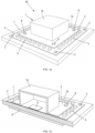
- a superconducting chip package 20 is illustrated in Figures 1a and 1b , respectively showing the outer appearance of the package 20 and a 3D section view.
- the package 20 is not in accordance with the invention and exhibits the disadvantages described above, as will be explained in more detail hereafter.
- the package comprises a square OFHC copper plate 1.
- a square PCB 2 is arranged and attached to the copper plate 1 by four screw connections 3 in the respective four corners of the PCB.
- the PCB 2 is one embodiment of the 'carrier substrate' stated in the appended claims, and may be a stripline PCB for example, or an embedded CPW PCB as referred to above in the introduction.
- Other types of carrier substrates may however be applied within the scope of the present invention.
- a general characteristic of the carrier substrate is that it comprises transmission lines for transmitting high frequency electrical signals, wherein said transmission lines are shielded from EM noise as a consequence of the design of the carrier, as is the case for the stripline PCB and embedded CPW PCB for example.
- LTCC low temperature co-fired ceramics
- micromachined stacked substrates with substrate vias or others.
- the PCB 2 is provided with four rows of electrical connectors 5, one row extending along each side, which are connected via electrical conductors (not shown) incorporated in the PCB, to a superconducting chip 6 mounted centrally on the PCB 2.
- the connectors 5 are represented in a simplified way as cylindrical structures protruding from the PCB surface and are in reality formed as suitable connectors configured to receive a matching connector coupled to an electrical wire.
- the chip 6 is shielded from external magnetic fields by a shield structure 7 comprising a planar support portion 7a and a receptacle shaped shell portion 7b placed above and around the chip location.
- the planar portion 7a extends outward from the rim of the shell portion 7b.
- the planar dimensions of the PCB 2 may for example be in the order of 10 x 10 cm, with larger dimensions of the planar support portion 7a of the shield structure 7 and of the OFHC plate 1 which may be in accordance with the image shown.
- the shield structure 7 is formed of a material that exhibits high magnetic permeability, and thus low reluctance, at cryogenic temperatures, down to the operational temperature of the superconducting chip 6 when the package is mounted on a dilution refrigerator stage.
- Relative permeability values required for the purpose of shielding operational superconducting chips are in the order of 80.000 to 100.000.
- Materials of this type are for example Nickel-based alloys of a specific composition and available under the name Cryoperm ® , which exhibit permeability in the order of the above-named values at the required cryogenic temperature.
- the planar support portion 7a of the shield structure 7 is placed on the PCB 2 and is attached by screw connections 8 to a shield plate 9 lying on the opposite side of the package, and formed of the same material as the shield structure 7 or of a material having the same high permeability properties at cryogenic temperatures.
- the PCB 2 and the OFHC plate 1 are thus sandwiched and clamped between a first shield structure 7 and a second shield structure 9 by a clamping force exhibited by the screw connections 8.
- the shield structure 7 and the lower shield plate 9 act to deflect stray magnetic field lines coming from external sources away from the superconducting chip 6.
- the low reluctance path between the shields 7 and 9 is broken by the PCB 2 and the OFHC plate 1 whose relative permeability value is about 1. Therefore, the effective shielding inside the shield shown in Fig. 1a and 1b is degraded due to field lines leaking into the shield through the PCB 2 and the OFHC plate 1.
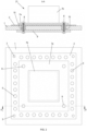
- Figure 2 shows a top view and section view of a superconducting chip package 21 in accordance with an embodiment of the invention.
- the components described above in relation to the package shown in Figure 1 are indicated by the same reference numerals. The above descriptions of these components are valid also for the package of Figure 2 .
- the package 21 comprises hollow cylindrical pillars 15 which penetrate the PCB 2 and the OFHC plate 1.
- the pillars 15 are clamped between and in physical contact with the planar support portion 7a of the shield structure 7 and the lower shield plate 9.
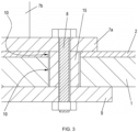
- a detail of the package in the vicinity of one of the pillars 15 is shown in Figure 3 .
- the holes 10 provided in the OFHC plate 1 and the PCB 2 for the passage of the screws of the screw connections 8 have a higher diameter than the same holes in the package of Figures 1a and 1b , to allow the passage of the pillars 15 through said holes 10.
- the screws of the screw connections 8 are inserted through the hollow pillars 15.
- a small air gap between the pillars 15 and the sidewalls of the holes 10 is permitted so that the pillars may be inserted into the holes by manual manipulation.
- the pillars 15 could be produced by filling the holes 10 with a high permeability material using for example plating or printing techniques.
- the material of the pillars 15 is a magnetic shielding material having high permeability at cryogenic temperatures, preferably it is the same material as the material of the shield structure 7 and/or the lower shield plate 9.
- the pillars 15 create a low reluctance path from the upper part of the package to the lower part, thereby improving the magnetic field attenuation inside the cavity of the shell portion 7b..
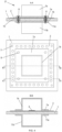
- Figure 4 illustrates a package 21 according to another embodiment of the invention.
- the figure includes a top view and two section views through respective section planes A-A and B-B.
- the lower shield plate 9 is replaced by a shield structure 11 that has the same shape as the shield structure 7, comprising a planar support portion 11a and a receptacle-shaped shell portion 11b.
- the shield structures are arranged in mirrored fashion on either side of the stack comprising the OFHC plate 1 and the PCB 2, and clamped together by the screw connections 8.
- low reluctance pillars 15 are present, this time clamped between and in physical contact with the planar shield support portions 7a and 11a.
- the effect may be further increased by increasing the number of pillars 15 and/or reducing the gap between the shield portions 7a and 11a (or 7a and 9 in the embodiment of Figure 2 ).
- Other ways of enhancing the effect may include applying multiple rows of pillars, possibly applying at least two rows which are staggered one with respect to the other.
- the number of pillars is however not limited to any particular number or range. Any number of pillars is possible that can be realistically applied in view of the dimensions of a particular package.
- the pillars are preferably but not exclusively arranged at regular intervals around the shell portion 7a of the upper shield structure 7.
- the dimensions of the pillars are also not limited to any particular value or range.
- the pillars 15 need not necessarily be shaped as hollow cylinders arranged around the screws of the screw connections 8. Pillars of the same shape, or of another shape may be clamped between the planar shield portions 7a and 11a (or 7a and 9) at other locations than the locations of the screw connections 8, although it is preferable to place the pillars as close as possible to said screw connections, as the clamping force is highest at these locations thereby minimising the leakage of magnetic field lines through the interfaces between the pillars 15 and the upper and lower shield structures 7 and 11 (or 7 and 9).
- the embodiment wherein the pillars are hollow cylinders 15 arranged around the screws represents a preferred version.
- Other possible shapes of pillars are full cylinders or rectangular blocks. The pillars do require planar upper and lower surfaces which can be placed in full contact with the upper and lower planar shield portions 7a and 11a (or 7a and 9).
- the pillars 15 are located as far away as possible from the superconducting chip(s) 6.
- the pillars 15 need not be formed as integral pieces of low reluctance material.
- the hollow cylindrical pillars 15 may be formed from a plurality of rings of said material stacked together. The latter approach may be applied also for producing pillars of other shapes, by stacking strips of the low reluctance material together and connecting them by a tack weld or the like
- Pillars may be produced in this way when the particular material does not allow the production of integral pieces having the required height corresponding to the width of the gap between the shield portions 7a and 11a (or 7a and 9).
- the invention is furthermore not limited to embodiments wherein the upper and lower shields are clamped together by screw connections 8.
- Other mechanical clamping means may be applied which clamp the upper and lower shields together in a reversable way, i.e. allowing the package to be disassembled and re-assembled.
- the invention is related to such a package, i.e. a package that can be disassembled and re-assembled, either containing one or more superconducting chips 6 mounted on the PCB 2 or without such chips mounted on the PCB.
- a package of the invention may however also be a package that is not configured to be disassembled, but wherein the upper and lower shields are clamped together by a permanent means, such as by welding, and wherein one or a plurality of low reluctance pillars is arranged between the permanently assembled shield portions.
- the shield structures on either side of the chip(s) 6 need not be exactly the same in shape in dimensions. More generally stated, embodiments of which Figure 4 shows an example comprise shield structures on both sides of the metal plate 1, said structures comprising mutually facing cavities formed by the shell portions (e.g. portions 7b, 11b in Fig. 4 ) of the respective shield structures.
- a second PCB comprising a second superconducting chip or set of superconducting chips could be arranged on the other side of the OFHC plate 1, wherein the second superconducting chip is shielded by the shell portion 11b of the second shield structure 11.
- the package 21 may further comprise an additional shield around the one or more superconducting chips 6 and formed inside the cavity of the shell portion 7b of the first shield structure 7.
- the additional shield is formed of a metal that may have superconducting properties at the cryogenic operational temperature of the superconducting chip or chips 6. Such materials are well known in the prior art, for example Al-based materials.
- the additional shield may be formed as a cage that is placed above and around the chip.
- the use of such a superconducting shield inside a high permeability shield is known as such, as a way of further increasing the level of attenuation of magnetic fields at the location of the chip or chips and at the cryogenic operational temperature of the chips.
- the additional shield material only obtains its superconducting properties below a given transition temperature.
- the high permeability shield 7 is therefore instrumental in creating a low magnetic field environment for the superconducting shield when it transitions from a normal metal to the superconducting state as the dilution refrigerator cools down below the transition temperature of the superconducting metal.
- the low magnetic environment minimizes the appearance of flux traps in the superconducting shield which could potentially cause the qubits to decohere.
- the background field is drastically reduced compared to a package that does not comprise the pillars, which increases the efficiency of the superconducting shield significantly.
- the additional shield inside the high permeability shield may be formed of a metal that does not have superconductive properties at the chip's operational temperature, such as copper.
- the additional shield inside the high permeability shield 7 could be omitted.
- additional, possibly superconducting shields may be added in the cavities of both the upper and lower high permeability shell portions 7b and 11b.
- the shape of the high permeability shell portion 7b or of both shell portions 7b and 11b in the embodiment of Figure 4 is not limited to the shape of a rectangular box. Any other receptacle shape may be applied instead of the one illustrated in the drawings.
- the shield structures 7 and 11 need not necessarily be identical in terms of their shape and dimensions.
Landscapes
- Shielding Devices Or Components To Electric Or Magnetic Fields (AREA)
Claims (9)
- Gehäuse (21), das einen oder mehrere supraleitende Chips (6) umfasst oder dazu konfiguriert ist, diese aufzunehmen, wobei das Gehäuse Folgendes umfasst:- ein Trägersubstrat (2), das einen oder mehrere darauf montierte supraleitende Chips (6) umfasst oder zum Montieren eines oder mehrerer supraleitender Chips (6) darauf geeignet ist,- eine Metallstützplatte (1), die eine Vorder- und eine Rückfläche aufweist, wobei das Trägersubstrat (2) auf der Vorderfläche der Metallstützplatte montiert ist, wobei die Metallstützplatte (1) dazu konfiguriert ist, mit einer Niedertemperaturstufe einer Kühleinrichtung gekoppelt zu werden,- eine erste Abschirmstruktur (7), die aus einem magnetischen Abschirmmaterial gebildet ist, einen behälterförmigen Schalenabschnitt (7b) und einen planaren Abschirmabschnitt (7a) umfasst, der sich vom Rand des Schalenabschnitts (7b) seitlich nach außen erstreckt, wobei das Innere des Schalenabschnitts (7b) einen Hohlraum bildet, der sich über und um die Stelle des einen oder der mehreren supraleitenden Chips (6) erstreckt,- eine zweite Abschirmstruktur (9, 11), die aus einem magnetischen Abschirmmaterial gebildet ist und mindestens einen zweiten planaren Abschirmabschnitt (9, 11a) umfasst,wobei:- das Trägersubstrat (2) und die Metallstützplatte (1) zwischen den ersten und zweiten planaren Abschirmsabschnitten (7a, 9; 7a, 11a) eingeklemmt sind,- eine Vielzahl von Säulen (15), die aus einem magnetischen Abschirmmaterial gebildet sind, zwischen den ersten und zweiten planaren Abschirmungsabschnitten eingeklemmt sind, wobei die Säulen (15):- das Trägersubstrat (2) und die Metallstützplatte (1) durchdringen,- in physischem Kontakt mit sowohl den ersten als auch zweiten planaren Abschirmabschnitten (7a, 9; 7a, 11a) sind.
- Gehäuse (21) nach Anspruch 1, wobei die Säulen die Form von Hohlzylindern (15) aufweisen und wobei die planaren Abschirmabschnitte (7a, 9; 7a, 11a) durch Schraubverbindungen (8) verspannt sind, die Schrauben umfassen, die durch die Hohlzylinder (15) eingesetzt werden.
- Gehäuse (21) nach Anspruch 1 oder 2, wobei die Säulen in regelmäßigen Abständen entlang des Umfangs des Schalenabschnitts (7b) der ersten Abschirmstruktur (7) verteilt sind.
- Gehäuse (21) nach einem der vorstehenden Ansprüche, wobei das Trägersubstrat (2) eine mehrschichtige Streifenleitungsleiterplatte ist.
- Gehäuse (21) nach einem der vorstehenden Ansprüche, wobei das Gehäuse weiter eine zusätzliche Abschirmung umfasst, die im Inneren des Schalenabschnitts (7b) der ersten Abschirmstruktur montiert ist.
- Gehäuse nach Anspruch 5, wobei die zusätzliche Abschirmung aus einem Metall gebildet ist, das unterhalb einer Übergangstemperatur supraleitende Eigenschaften annimmt.
- Gehäuse (21) nach einem der vorstehenden Ansprüche, wobei die zweite Abschirmstruktur (11) einen zweiten behälterförmigen Schalenabschnitt (11b) umfasst, wobei sich der zweite planare Abschirmabschnitt (11a) der zweiten Struktur vom Rand des zweiten Schalenabschnitts (11b) nach außen erstreckt, und wobei die Abschirmstrukturen (7, 11), wobei das Innere des zweiten Schalenabschnitts (11b) einen Hohlraum bildet, der sich auf der anderen Seite der Metallstützplatte (1) und gegenüber des Hohlraums erstreckt, der durch den ersten Schalenabschnitt (7b) gebildet wird.
- Gehäuse (21) nach Anspruch 6, wobei das Gehäuse weiter eine zusätzliche Abschirmung umfasst, die im Inneren des zweiten Schalenabschnitts (11b) montiert ist, wobei die zusätzliche Abschirmung aus einem Metall gebildet ist, das unterhalb einer Übergangstemperatur supraleitende Eigenschaften annimmt.
- Gehäuse (21) nach einem der vorstehenden Ansprüche, wobei das Trägersubstrat (2) eine Vielzahl von Verbindern (5) zur Verbindung des Trägersubstrats (2) an eine oder mehrere externe Einrichtungen umfasst.
Priority Applications (3)
| Application Number | Priority Date | Filing Date | Title |
|---|---|---|---|
| EP21210843.5A EP4187451B1 (de) | 2021-11-26 | 2021-11-26 | Supraleitendes chip-gehäuse mit verbesserter magnetischer abschirmung |
| CN202211324035.1A CN116193975A (zh) | 2021-11-26 | 2022-10-27 | 具有经改进磁屏蔽的超导芯片封装 |
| US18/055,961 US12317756B2 (en) | 2021-11-26 | 2022-11-16 | Superconducting chip package with improved magnetic shielding |
Applications Claiming Priority (1)
| Application Number | Priority Date | Filing Date | Title |
|---|---|---|---|
| EP21210843.5A EP4187451B1 (de) | 2021-11-26 | 2021-11-26 | Supraleitendes chip-gehäuse mit verbesserter magnetischer abschirmung |
Publications (2)
| Publication Number | Publication Date |
|---|---|
| EP4187451A1 EP4187451A1 (de) | 2023-05-31 |
| EP4187451B1 true EP4187451B1 (de) | 2024-06-26 |
Family
ID=78820758
Family Applications (1)
| Application Number | Title | Priority Date | Filing Date |
|---|---|---|---|
| EP21210843.5A Active EP4187451B1 (de) | 2021-11-26 | 2021-11-26 | Supraleitendes chip-gehäuse mit verbesserter magnetischer abschirmung |
Country Status (3)
| Country | Link |
|---|---|
| US (1) | US12317756B2 (de) |
| EP (1) | EP4187451B1 (de) |
| CN (1) | CN116193975A (de) |
Cited By (1)
| Publication number | Priority date | Publication date | Assignee | Title |
|---|---|---|---|---|
| RU2854290C1 (ru) * | 2025-07-02 | 2025-12-29 | Акционерное общество "СИКВЭЛ" | Держатель сверхпроводниковых микросхем |
Families Citing this family (1)
| Publication number | Priority date | Publication date | Assignee | Title |
|---|---|---|---|---|
| FR3166223A1 (fr) * | 2024-09-11 | 2026-03-13 | C12 Quantum Electronics | Mécanisme et procédé permettant de fermer une boîte prévue pour contenir un composant ou circuit de qubit |
Family Cites Families (6)
| Publication number | Priority date | Publication date | Assignee | Title |
|---|---|---|---|---|
| US10692795B2 (en) * | 2018-11-13 | 2020-06-23 | International Business Machines Corporation | Flip chip assembly of quantum computing devices |
| JP7528557B2 (ja) * | 2020-06-19 | 2024-08-06 | 日本電気株式会社 | 量子デバイス及びその製造方法 |
| JP7468193B2 (ja) * | 2020-06-29 | 2024-04-16 | 日本電気株式会社 | 量子デバイス及びその製造方法 |
| US11152707B1 (en) * | 2020-07-02 | 2021-10-19 | International Business Machines Corporation | Fast radio frequency package |
| US11676903B2 (en) * | 2020-08-20 | 2023-06-13 | International Business Machines Corporation | Combined backing plate and housing for use in bump bonded chip assembly |
| CN213782007U (zh) * | 2020-12-07 | 2021-07-23 | 中国电子科技集团公司第四十三研究所 | 一种超导量子计算芯片用封装结构 |
-
2021
- 2021-11-26 EP EP21210843.5A patent/EP4187451B1/de active Active
-
2022
- 2022-10-27 CN CN202211324035.1A patent/CN116193975A/zh active Pending
- 2022-11-16 US US18/055,961 patent/US12317756B2/en active Active
Cited By (1)
| Publication number | Priority date | Publication date | Assignee | Title |
|---|---|---|---|---|
| RU2854290C1 (ru) * | 2025-07-02 | 2025-12-29 | Акционерное общество "СИКВЭЛ" | Держатель сверхпроводниковых микросхем |
Also Published As
| Publication number | Publication date |
|---|---|
| US12317756B2 (en) | 2025-05-27 |
| CN116193975A (zh) | 2023-05-30 |
| US20230270020A1 (en) | 2023-08-24 |
| EP4187451A1 (de) | 2023-05-31 |
Similar Documents
| Publication | Publication Date | Title |
|---|---|---|
| US11362257B2 (en) | Quantum bit device | |
| AU769351B2 (en) | Integrated convection and conduction heat sink for multiple mounting positions | |
| Al-Sarawi et al. | A review of 3-D packaging technology | |
| US11557709B2 (en) | Flexible wiring for low temperature applications | |
| US4771365A (en) | Passive cooled electronic chassis | |
| EP0367630A1 (de) | Packung für elektronische Anordnungen zum Betrieb bei verschiedenen jeweiligen Temperaturen | |
| WO2019004991A1 (en) | ASSEMBLIES OF QUANTUM CALCULATORS | |
| KR102468955B1 (ko) | 강제 흐름 냉각 온도 제어 방법, 시스템, 및 장치 | |
| US12424604B2 (en) | Systems and methods for assembling processor systems | |
| US20220230785A1 (en) | High-Density Cryogenic Wiring for Superconducting Qubit Control | |
| EP4187451B1 (de) | Supraleitendes chip-gehäuse mit verbesserter magnetischer abschirmung | |
| EP3847722B1 (de) | Rf schaltkreismodul umfassend einer leiterplatte | |
| US11678433B2 (en) | Printed circuit board assembly for edge-coupling to an integrated circuit | |
| JP2022167705A (ja) | 量子デバイス | |
| US12193339B1 (en) | Integrated readout card | |
| US12096551B2 (en) | Trans-vacuum printed flexible wiring apparatus | |
| US11864352B1 (en) | Cryostat suspended sample board | |
| US20240288213A1 (en) | Cryostat socket for holding an ion trap device mounted on a substrate in a cryostat | |
| EP3696844A1 (de) | Stromeinleitungsanschluss und damit versehene druckhaltevorrichtung sowie röntgenbilderfassungsvorrichtung | |
| CN205232575U (zh) | 电子装置、电子系统和电子设施 | |
| US20040189418A1 (en) | Method and structure for implementing enhanced differential signal trace routing | |
| JP7315666B2 (ja) | マイクロ波回路用の信号コネクタ | |
| US12016138B2 (en) | Printed flexible wiring apparatus in a cryostat | |
| WO2025163247A1 (en) | A cable connector assembly | |
| Filatova et al. | Modern Cryogenic Electronics Patents Survey |
Legal Events
| Date | Code | Title | Description |
|---|---|---|---|
| PUAI | Public reference made under article 153(3) epc to a published international application that has entered the european phase |
Free format text: ORIGINAL CODE: 0009012 |
|
| STAA | Information on the status of an ep patent application or granted ep patent |
Free format text: STATUS: THE APPLICATION HAS BEEN PUBLISHED |
|
| AK | Designated contracting states |
Kind code of ref document: A1 Designated state(s): AL AT BE BG CH CY CZ DE DK EE ES FI FR GB GR HR HU IE IS IT LI LT LU LV MC MK MT NL NO PL PT RO RS SE SI SK SM TR |
|
| STAA | Information on the status of an ep patent application or granted ep patent |
Free format text: STATUS: REQUEST FOR EXAMINATION WAS MADE |
|
| 17P | Request for examination filed |
Effective date: 20231004 |
|
| RBV | Designated contracting states (corrected) |
Designated state(s): AL AT BE BG CH CY CZ DE DK EE ES FI FR GB GR HR HU IE IS IT LI LT LU LV MC MK MT NL NO PL PT RO RS SE SI SK SM TR |
|
| GRAP | Despatch of communication of intention to grant a patent |
Free format text: ORIGINAL CODE: EPIDOSNIGR1 |
|
| STAA | Information on the status of an ep patent application or granted ep patent |
Free format text: STATUS: GRANT OF PATENT IS INTENDED |
|
| INTG | Intention to grant announced |
Effective date: 20240229 |
|
| P01 | Opt-out of the competence of the unified patent court (upc) registered |
Effective date: 20240328 |
|
| GRAS | Grant fee paid |
Free format text: ORIGINAL CODE: EPIDOSNIGR3 |
|
| GRAA | (expected) grant |
Free format text: ORIGINAL CODE: 0009210 |
|
| STAA | Information on the status of an ep patent application or granted ep patent |
Free format text: STATUS: THE PATENT HAS BEEN GRANTED |
|
| AK | Designated contracting states |
Kind code of ref document: B1 Designated state(s): AL AT BE BG CH CY CZ DE DK EE ES FI FR GB GR HR HU IE IS IT LI LT LU LV MC MK MT NL NO PL PT RO RS SE SI SK SM TR |
|
| REG | Reference to a national code |
Ref country code: GB Ref legal event code: FG4D |
|
| REG | Reference to a national code |
Ref country code: CH Ref legal event code: EP |
|
| REG | Reference to a national code |
Ref country code: DE Ref legal event code: R096 Ref document number: 602021014786 Country of ref document: DE |
|
| PG25 | Lapsed in a contracting state [announced via postgrant information from national office to epo] |
Ref country code: BG Free format text: LAPSE BECAUSE OF FAILURE TO SUBMIT A TRANSLATION OF THE DESCRIPTION OR TO PAY THE FEE WITHIN THE PRESCRIBED TIME-LIMIT Effective date: 20240626 |
|
| PG25 | Lapsed in a contracting state [announced via postgrant information from national office to epo] |
Ref country code: FI Free format text: LAPSE BECAUSE OF FAILURE TO SUBMIT A TRANSLATION OF THE DESCRIPTION OR TO PAY THE FEE WITHIN THE PRESCRIBED TIME-LIMIT Effective date: 20240626 Ref country code: HR Free format text: LAPSE BECAUSE OF FAILURE TO SUBMIT A TRANSLATION OF THE DESCRIPTION OR TO PAY THE FEE WITHIN THE PRESCRIBED TIME-LIMIT Effective date: 20240626 |
|
| REG | Reference to a national code |
Ref country code: LT Ref legal event code: MG9D |
|
| PG25 | Lapsed in a contracting state [announced via postgrant information from national office to epo] |
Ref country code: GR Free format text: LAPSE BECAUSE OF FAILURE TO SUBMIT A TRANSLATION OF THE DESCRIPTION OR TO PAY THE FEE WITHIN THE PRESCRIBED TIME-LIMIT Effective date: 20240927 |
|
| PG25 | Lapsed in a contracting state [announced via postgrant information from national office to epo] |
Ref country code: LV Free format text: LAPSE BECAUSE OF FAILURE TO SUBMIT A TRANSLATION OF THE DESCRIPTION OR TO PAY THE FEE WITHIN THE PRESCRIBED TIME-LIMIT Effective date: 20240626 |
|
| REG | Reference to a national code |
Ref country code: NL Ref legal event code: MP Effective date: 20240626 |
|
| PG25 | Lapsed in a contracting state [announced via postgrant information from national office to epo] |
Ref country code: NO Free format text: LAPSE BECAUSE OF FAILURE TO SUBMIT A TRANSLATION OF THE DESCRIPTION OR TO PAY THE FEE WITHIN THE PRESCRIBED TIME-LIMIT Effective date: 20240926 Ref country code: LV Free format text: LAPSE BECAUSE OF FAILURE TO SUBMIT A TRANSLATION OF THE DESCRIPTION OR TO PAY THE FEE WITHIN THE PRESCRIBED TIME-LIMIT Effective date: 20240626 Ref country code: HR Free format text: LAPSE BECAUSE OF FAILURE TO SUBMIT A TRANSLATION OF THE DESCRIPTION OR TO PAY THE FEE WITHIN THE PRESCRIBED TIME-LIMIT Effective date: 20240626 Ref country code: GR Free format text: LAPSE BECAUSE OF FAILURE TO SUBMIT A TRANSLATION OF THE DESCRIPTION OR TO PAY THE FEE WITHIN THE PRESCRIBED TIME-LIMIT Effective date: 20240927 Ref country code: FI Free format text: LAPSE BECAUSE OF FAILURE TO SUBMIT A TRANSLATION OF THE DESCRIPTION OR TO PAY THE FEE WITHIN THE PRESCRIBED TIME-LIMIT Effective date: 20240626 Ref country code: BG Free format text: LAPSE BECAUSE OF FAILURE TO SUBMIT A TRANSLATION OF THE DESCRIPTION OR TO PAY THE FEE WITHIN THE PRESCRIBED TIME-LIMIT Effective date: 20240626 Ref country code: RS Free format text: LAPSE BECAUSE OF FAILURE TO SUBMIT A TRANSLATION OF THE DESCRIPTION OR TO PAY THE FEE WITHIN THE PRESCRIBED TIME-LIMIT Effective date: 20240926 |
|
| PG25 | Lapsed in a contracting state [announced via postgrant information from national office to epo] |
Ref country code: NL Free format text: LAPSE BECAUSE OF FAILURE TO SUBMIT A TRANSLATION OF THE DESCRIPTION OR TO PAY THE FEE WITHIN THE PRESCRIBED TIME-LIMIT Effective date: 20240626 |
|
| REG | Reference to a national code |
Ref country code: AT Ref legal event code: MK05 Ref document number: 1698337 Country of ref document: AT Kind code of ref document: T Effective date: 20240626 |
|
| PG25 | Lapsed in a contracting state [announced via postgrant information from national office to epo] |
Ref country code: NL Free format text: LAPSE BECAUSE OF FAILURE TO SUBMIT A TRANSLATION OF THE DESCRIPTION OR TO PAY THE FEE WITHIN THE PRESCRIBED TIME-LIMIT Effective date: 20240626 |
|
| PG25 | Lapsed in a contracting state [announced via postgrant information from national office to epo] |
Ref country code: PT Free format text: LAPSE BECAUSE OF FAILURE TO SUBMIT A TRANSLATION OF THE DESCRIPTION OR TO PAY THE FEE WITHIN THE PRESCRIBED TIME-LIMIT Effective date: 20241028 |
|
| PG25 | Lapsed in a contracting state [announced via postgrant information from national office to epo] |
Ref country code: PT Free format text: LAPSE BECAUSE OF FAILURE TO SUBMIT A TRANSLATION OF THE DESCRIPTION OR TO PAY THE FEE WITHIN THE PRESCRIBED TIME-LIMIT Effective date: 20241028 |
|
| PG25 | Lapsed in a contracting state [announced via postgrant information from national office to epo] |
Ref country code: PL Free format text: LAPSE BECAUSE OF FAILURE TO SUBMIT A TRANSLATION OF THE DESCRIPTION OR TO PAY THE FEE WITHIN THE PRESCRIBED TIME-LIMIT Effective date: 20240626 |
|
| PG25 | Lapsed in a contracting state [announced via postgrant information from national office to epo] |
Ref country code: EE Free format text: LAPSE BECAUSE OF FAILURE TO SUBMIT A TRANSLATION OF THE DESCRIPTION OR TO PAY THE FEE WITHIN THE PRESCRIBED TIME-LIMIT Effective date: 20240626 |
|
| PG25 | Lapsed in a contracting state [announced via postgrant information from national office to epo] |
Ref country code: IS Free format text: LAPSE BECAUSE OF FAILURE TO SUBMIT A TRANSLATION OF THE DESCRIPTION OR TO PAY THE FEE WITHIN THE PRESCRIBED TIME-LIMIT Effective date: 20241026 Ref country code: AT Free format text: LAPSE BECAUSE OF FAILURE TO SUBMIT A TRANSLATION OF THE DESCRIPTION OR TO PAY THE FEE WITHIN THE PRESCRIBED TIME-LIMIT Effective date: 20240626 |
|
| PG25 | Lapsed in a contracting state [announced via postgrant information from national office to epo] |
Ref country code: CZ Free format text: LAPSE BECAUSE OF FAILURE TO SUBMIT A TRANSLATION OF THE DESCRIPTION OR TO PAY THE FEE WITHIN THE PRESCRIBED TIME-LIMIT Effective date: 20240626 |
|
| PG25 | Lapsed in a contracting state [announced via postgrant information from national office to epo] |
Ref country code: RO Free format text: LAPSE BECAUSE OF FAILURE TO SUBMIT A TRANSLATION OF THE DESCRIPTION OR TO PAY THE FEE WITHIN THE PRESCRIBED TIME-LIMIT Effective date: 20240626 Ref country code: SK Free format text: LAPSE BECAUSE OF FAILURE TO SUBMIT A TRANSLATION OF THE DESCRIPTION OR TO PAY THE FEE WITHIN THE PRESCRIBED TIME-LIMIT Effective date: 20240626 |
|
| PG25 | Lapsed in a contracting state [announced via postgrant information from national office to epo] |
Ref country code: SM Free format text: LAPSE BECAUSE OF FAILURE TO SUBMIT A TRANSLATION OF THE DESCRIPTION OR TO PAY THE FEE WITHIN THE PRESCRIBED TIME-LIMIT Effective date: 20240626 Ref country code: ES Free format text: LAPSE BECAUSE OF FAILURE TO SUBMIT A TRANSLATION OF THE DESCRIPTION OR TO PAY THE FEE WITHIN THE PRESCRIBED TIME-LIMIT Effective date: 20240626 |
|
| PG25 | Lapsed in a contracting state [announced via postgrant information from national office to epo] |
Ref country code: SM Free format text: LAPSE BECAUSE OF FAILURE TO SUBMIT A TRANSLATION OF THE DESCRIPTION OR TO PAY THE FEE WITHIN THE PRESCRIBED TIME-LIMIT Effective date: 20240626 Ref country code: SK Free format text: LAPSE BECAUSE OF FAILURE TO SUBMIT A TRANSLATION OF THE DESCRIPTION OR TO PAY THE FEE WITHIN THE PRESCRIBED TIME-LIMIT Effective date: 20240626 Ref country code: RO Free format text: LAPSE BECAUSE OF FAILURE TO SUBMIT A TRANSLATION OF THE DESCRIPTION OR TO PAY THE FEE WITHIN THE PRESCRIBED TIME-LIMIT Effective date: 20240626 Ref country code: PL Free format text: LAPSE BECAUSE OF FAILURE TO SUBMIT A TRANSLATION OF THE DESCRIPTION OR TO PAY THE FEE WITHIN THE PRESCRIBED TIME-LIMIT Effective date: 20240626 Ref country code: IS Free format text: LAPSE BECAUSE OF FAILURE TO SUBMIT A TRANSLATION OF THE DESCRIPTION OR TO PAY THE FEE WITHIN THE PRESCRIBED TIME-LIMIT Effective date: 20241026 Ref country code: ES Free format text: LAPSE BECAUSE OF FAILURE TO SUBMIT A TRANSLATION OF THE DESCRIPTION OR TO PAY THE FEE WITHIN THE PRESCRIBED TIME-LIMIT Effective date: 20240626 Ref country code: EE Free format text: LAPSE BECAUSE OF FAILURE TO SUBMIT A TRANSLATION OF THE DESCRIPTION OR TO PAY THE FEE WITHIN THE PRESCRIBED TIME-LIMIT Effective date: 20240626 Ref country code: CZ Free format text: LAPSE BECAUSE OF FAILURE TO SUBMIT A TRANSLATION OF THE DESCRIPTION OR TO PAY THE FEE WITHIN THE PRESCRIBED TIME-LIMIT Effective date: 20240626 Ref country code: AT Free format text: LAPSE BECAUSE OF FAILURE TO SUBMIT A TRANSLATION OF THE DESCRIPTION OR TO PAY THE FEE WITHIN THE PRESCRIBED TIME-LIMIT Effective date: 20240626 |
|
| PG25 | Lapsed in a contracting state [announced via postgrant information from national office to epo] |
Ref country code: IT Free format text: LAPSE BECAUSE OF FAILURE TO SUBMIT A TRANSLATION OF THE DESCRIPTION OR TO PAY THE FEE WITHIN THE PRESCRIBED TIME-LIMIT Effective date: 20240626 |
|
| REG | Reference to a national code |
Ref country code: DE Ref legal event code: R097 Ref document number: 602021014786 Country of ref document: DE |
|
| PG25 | Lapsed in a contracting state [announced via postgrant information from national office to epo] |
Ref country code: DK Free format text: LAPSE BECAUSE OF FAILURE TO SUBMIT A TRANSLATION OF THE DESCRIPTION OR TO PAY THE FEE WITHIN THE PRESCRIBED TIME-LIMIT Effective date: 20240626 |
|
| PLBE | No opposition filed within time limit |
Free format text: ORIGINAL CODE: 0009261 |
|
| STAA | Information on the status of an ep patent application or granted ep patent |
Free format text: STATUS: NO OPPOSITION FILED WITHIN TIME LIMIT |
|
| 26N | No opposition filed |
Effective date: 20250327 |
|
| REG | Reference to a national code |
Ref country code: CH Ref legal event code: PL |
|
| PG25 | Lapsed in a contracting state [announced via postgrant information from national office to epo] |
Ref country code: MC Free format text: LAPSE BECAUSE OF FAILURE TO SUBMIT A TRANSLATION OF THE DESCRIPTION OR TO PAY THE FEE WITHIN THE PRESCRIBED TIME-LIMIT Effective date: 20240626 |
|
| PG25 | Lapsed in a contracting state [announced via postgrant information from national office to epo] |
Ref country code: LU Free format text: LAPSE BECAUSE OF NON-PAYMENT OF DUE FEES Effective date: 20241126 |
|
| REG | Reference to a national code |
Ref country code: CH Ref legal event code: PL |
|
| PG25 | Lapsed in a contracting state [announced via postgrant information from national office to epo] |
Ref country code: CH Free format text: LAPSE BECAUSE OF NON-PAYMENT OF DUE FEES Effective date: 20241130 |
|
| REG | Reference to a national code |
Ref country code: BE Ref legal event code: MM Effective date: 20241130 |
|
| PG25 | Lapsed in a contracting state [announced via postgrant information from national office to epo] |
Ref country code: SE Free format text: LAPSE BECAUSE OF FAILURE TO SUBMIT A TRANSLATION OF THE DESCRIPTION OR TO PAY THE FEE WITHIN THE PRESCRIBED TIME-LIMIT Effective date: 20240626 |
|
| PG25 | Lapsed in a contracting state [announced via postgrant information from national office to epo] |
Ref country code: BE Free format text: LAPSE BECAUSE OF NON-PAYMENT OF DUE FEES Effective date: 20241130 |
|
| PG25 | Lapsed in a contracting state [announced via postgrant information from national office to epo] |
Ref country code: FR Free format text: LAPSE BECAUSE OF NON-PAYMENT OF DUE FEES Effective date: 20241130 |
|
| PG25 | Lapsed in a contracting state [announced via postgrant information from national office to epo] |
Ref country code: IE Free format text: LAPSE BECAUSE OF NON-PAYMENT OF DUE FEES Effective date: 20241126 |
|
| PGFP | Annual fee paid to national office [announced via postgrant information from national office to epo] |
Ref country code: DE Payment date: 20251022 Year of fee payment: 5 |
|
| PG25 | Lapsed in a contracting state [announced via postgrant information from national office to epo] |
Ref country code: HU Free format text: LAPSE BECAUSE OF FAILURE TO SUBMIT A TRANSLATION OF THE DESCRIPTION OR TO PAY THE FEE WITHIN THE PRESCRIBED TIME-LIMIT; INVALID AB INITIO Effective date: 20211126 |
|
| PG25 | Lapsed in a contracting state [announced via postgrant information from national office to epo] |
Ref country code: CY Free format text: LAPSE BECAUSE OF FAILURE TO SUBMIT A TRANSLATION OF THE DESCRIPTION OR TO PAY THE FEE WITHIN THE PRESCRIBED TIME-LIMIT; INVALID AB INITIO Effective date: 20211126 |